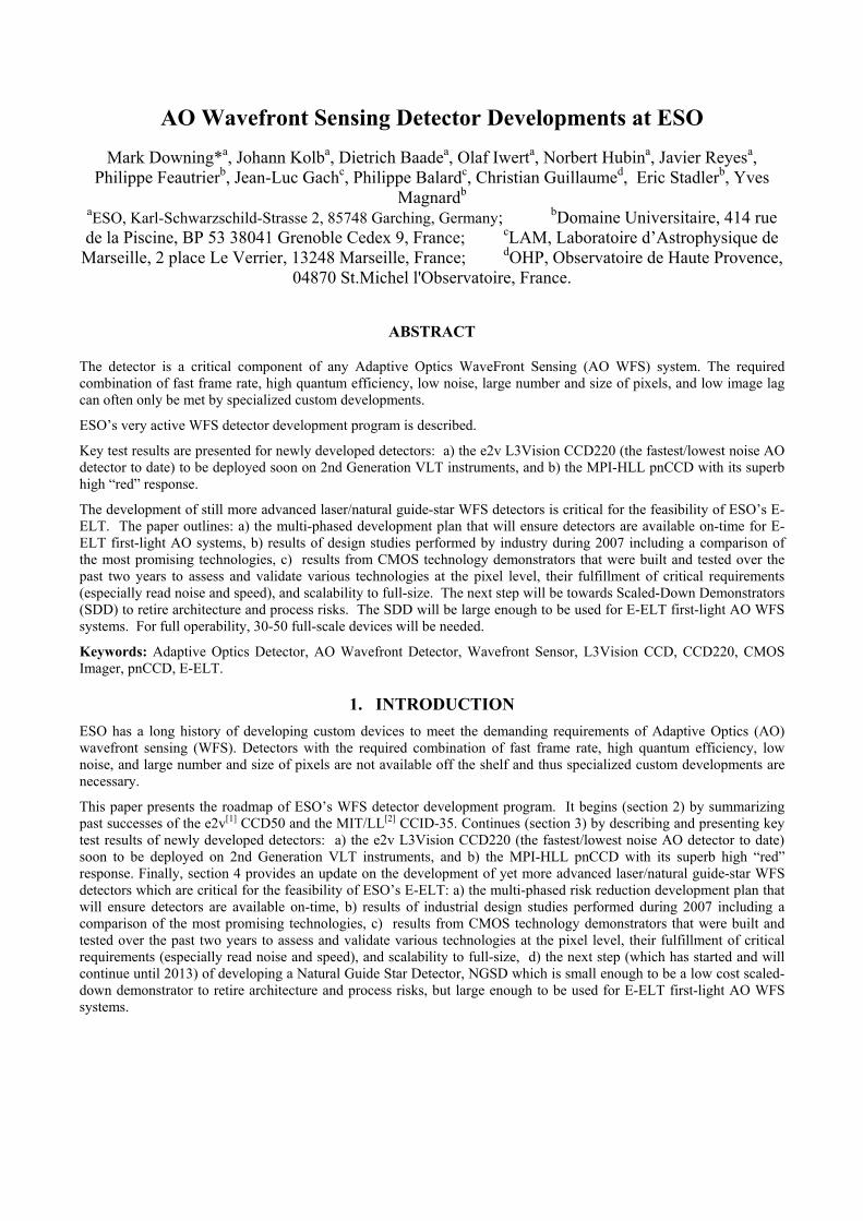
AO Wavefront Sensing Detector Developments at ESO · AO Wavefront Sensing Detector Developments at...
12
AO Wavefront Sensing Detector Developments at ESO Mark Downing* a , Johann Kolb a , Dietrich Baade a , Olaf Iwert a , Norbert Hubin a , Javier Reyes a , Philippe Feautrier b , Jean-Luc Gach c , Philippe Balard c , Christian Guillaume d , Eric Stadler b , Yves Magnard b a ESO, Karl-Schwarzschild-Strasse 2, 85748 Garching, Germany; b Domaine Universitaire, 414 rue de la Piscine, BP 53 38041 Grenoble Cedex 9, France; c LAM, Laboratoire d’Astrophysique de Marseille, 2 place Le Verrier, 13248 Marseille, France; d OHP, Observatoire de Haute Provence, 04870 St.Michel l'Observatoire, France. ABSTRACT The detector is a critical component of any Adaptive Optics WaveFront Sensing (AO WFS) system. The required combination of fast frame rate, high quantum efficiency, low noise, large number and size of pixels, and low image lag can often only be met by specialized custom developments. ESO’s very active WFS detector development program is described. Key test results are presented for newly developed detectors: a) the e2v L3Vision CCD220 (the fastest/lowest noise AO detector to date) to be deployed soon on 2nd Generation VLT instruments, and b) the MPI-HLL pnCCD with its superb high “red” response. The development of still more advanced laser/natural guide-star WFS detectors is critical for the feasibility of ESO’s E- ELT. The paper outlines: a) the multi-phased development plan that will ensure detectors are available on-time for E- ELT first-light AO systems, b) results of design studies performed by industry during 2007 including a comparison of the most promising technologies, c) results from CMOS technology demonstrators that were built and tested over the past two years to assess and validate various technologies at the pixel level, their fulfillment of critical requirements (especially read noise and speed), and scalability to full-size. The next step will be towards Scaled-Down Demonstrators (SDD) to retire architecture and process risks. The SDD will be large enough to be used for E-ELT first-light AO WFS systems. For full operability, 30-50 full-scale devices will be needed. Keywords: Adaptive Optics Detector, AO Wavefront Detector, Wavefront Sensor, L3Vision CCD, CCD220, CMOS Imager, pnCCD, E-ELT. 1. INTRODUCTION ESO has a long history of developing custom devices to meet the demanding requirements of Adaptive Optics (AO) wavefront sensing (WFS). Detectors with the required combination of fast frame rate, high quantum efficiency, low noise, and large number and size of pixels are not available off the shelf and thus specialized custom developments are necessary. This paper presents the roadmap of ESO’s WFS detector development program. It begins (section 2) by summarizing past successes of the e2v [1] CCD50 and the MIT/LL [2] CCID-35. Continues (section 3) by describing and presenting key test results of newly developed detectors: a) the e2v L3Vision CCD220 (the fastest/lowest noise AO detector to date) soon to be deployed on 2nd Generation VLT instruments, and b) the MPI-HLL pnCCD with its superb high “red” response. Finally, section 4 provides an update on the development of yet more advanced laser/natural guide-star WFS detectors which are critical for the feasibility of ESO’s E-ELT: a) the multi-phased risk reduction development plan that will ensure detectors are available on-time, b) results of industrial design studies performed during 2007 including a comparison of the most promising technologies, c) results from CMOS technology demonstrators that were built and tested over the past two years to assess and validate various technologies at the pixel level, their fulfillment of critical requirements (especially read noise and speed), and scalability to full-size, d) the next step (which has started and will continue until 2013) of developing a Natural Guide Star Detector, NGSD which is small enough to be a low cost scaled- down demonstrator to retire architecture and process risks, but large enough to be used for E-ELT first-light AO WFS systems.
Transcript of AO Wavefront Sensing Detector Developments at ESO · AO Wavefront Sensing Detector Developments at...
AO Wavefront Sensing Detector Developments at ESO
Mark Downing*a, Johann Kolba, Dietrich Baadea, Olaf Iwerta, Norbert Hubina, Javier Reyesa, Philippe Feautrierb, Jean-Luc Gachc, Philippe Balardc, Christian Guillaumed, Eric Stadlerb, Yves
Magnardb aESO, Karl-Schwarzschild-Strasse 2, 85748 Garching, Germany; bDomaine Universitaire, 414 rue de la Piscine, BP 53 38041 Grenoble Cedex 9, France; cLAM, Laboratoire d’Astrophysique de
Marseille, 2 place Le Verrier, 13248 Marseille, France; dOHP, Observatoire de Haute Provence, 04870 St.Michel l'Observatoire, France.
ABSTRACT
The detector is a critical component of any Adaptive Optics WaveFront Sensing (AO WFS) system. The required combination of fast frame rate, high quantum efficiency, low noise, large number and size of pixels, and low image lag can often only be met by specialized custom developments.
ESO’s very active WFS detector development program is described.
Key test results are presented for newly developed detectors: a) the e2v L3Vision CCD220 (the fastest/lowest noise AO detector to date) to be deployed soon on 2nd Generation VLT instruments, and b) the MPI-HLL pnCCD with its superb high “red” response.
The development of still more advanced laser/natural guide-star WFS detectors is critical for the feasibility of ESO’s E-ELT. The paper outlines: a) the multi-phased development plan that will ensure detectors are available on-time for E-ELT first-light AO systems, b) results of design studies performed by industry during 2007 including a comparison of the most promising technologies, c) results from CMOS technology demonstrators that were built and tested over the past two years to assess and validate various technologies at the pixel level, their fulfillment of critical requirements (especially read noise and speed), and scalability to full-size. The next step will be towards Scaled-Down Demonstrators (SDD) to retire architecture and process risks. The SDD will be large enough to be used for E-ELT first-light AO WFS systems. For full operability, 30-50 full-scale devices will be needed.
Keywords: Adaptive Optics Detector, AO Wavefront Detector, Wavefront Sensor, L3Vision CCD, CCD220, CMOS Imager, pnCCD, E-ELT.
1. INTRODUCTION ESO has a long history of developing custom devices to meet the demanding requirements of Adaptive Optics (AO) wavefront sensing (WFS). Detectors with the required combination of fast frame rate, high quantum efficiency, low noise, and large number and size of pixels are not available off the shelf and thus specialized custom developments are necessary.
This paper presents the roadmap of ESO’s WFS detector development program. It begins (section 2) by summarizing past successes of the e2v[1] CCD50 and the MIT/LL[2] CCID-35. Continues (section 3) by describing and presenting key test results of newly developed detectors: a) the e2v L3Vision CCD220 (the fastest/lowest noise AO detector to date) soon to be deployed on 2nd Generation VLT instruments, and b) the MPI-HLL pnCCD with its superb high “red” response. Finally, section 4 provides an update on the development of yet more advanced laser/natural guide-star WFS detectors which are critical for the feasibility of ESO’s E-ELT: a) the multi-phased risk reduction development plan that will ensure detectors are available on-time, b) results of industrial design studies performed during 2007 including a comparison of the most promising technologies, c) results from CMOS technology demonstrators that were built and tested over the past two years to assess and validate various technologies at the pixel level, their fulfillment of critical requirements (especially read noise and speed), and scalability to full-size, d) the next step (which has started and will continue until 2013) of developing a Natural Guide Star Detector, NGSD which is small enough to be a low cost scaled-down demonstrator to retire architecture and process risks, but large enough to be used for E-ELT first-light AO WFS systems.
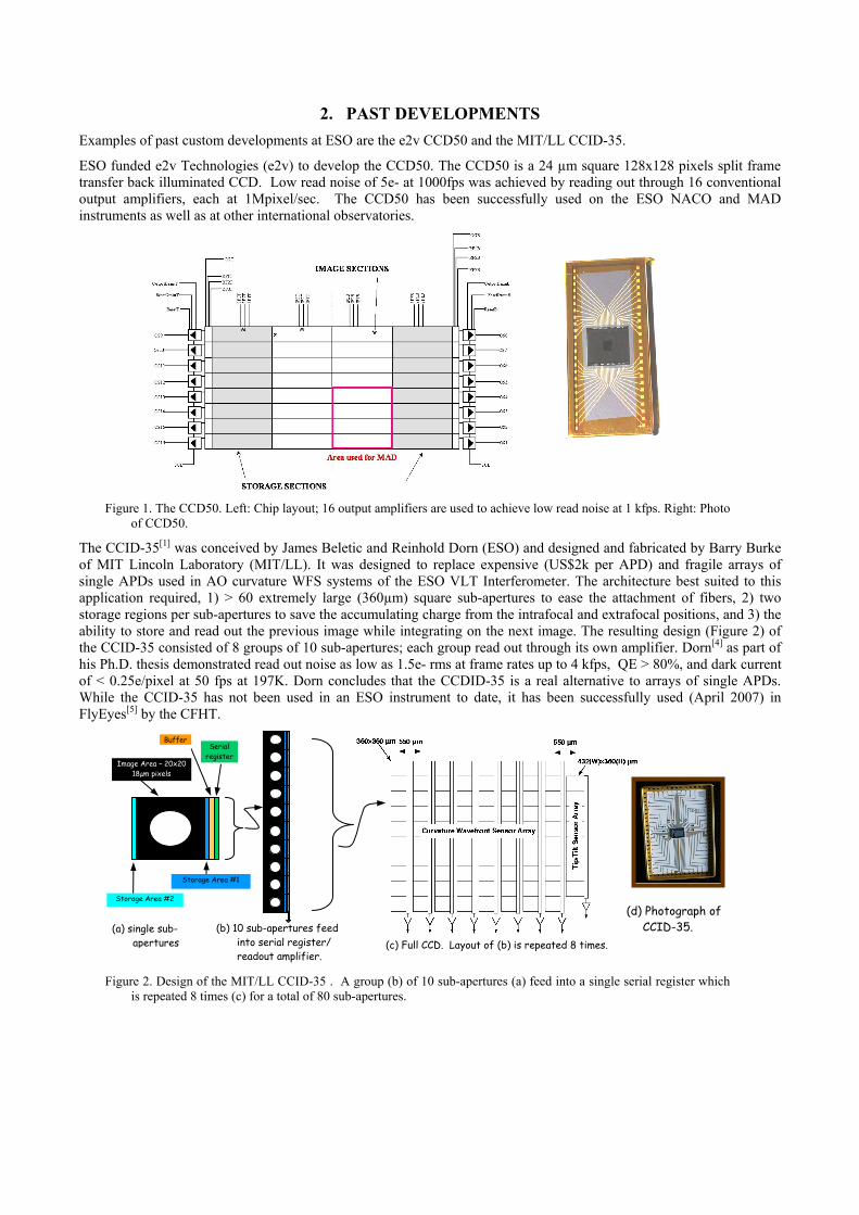
2. PAST DEVELOPMENTS Examples of past custom developments at ESO are the e2v CCD50 and the MIT/LL CCID-35.
ESO funded e2v Technologies (e2v) to develop the CCD50. The CCD50 is a 24 µm square 128x128 pixels split frame transfer back illuminated CCD. Low read noise of 5e- at 1000fps was achieved by reading out through 16 conventional output amplifiers, each at 1Mpixel/sec. The CCD50 has been successfully used on the ESO NACO and MAD instruments as well as at other international observatories.
Figure 1. The CCD50. Left: Chip layout; 16 output amplifiers are used to achieve low read noise at 1 kfps. Right: Photo
of CCD50.
The CCID-35[1] was conceived by James Beletic and Reinhold Dorn (ESO) and designed and fabricated by Barry Burke of MIT Lincoln Laboratory (MIT/LL). It was designed to replace expensive (US$2k per APD) and fragile arrays of single APDs used in AO curvature WFS systems of the ESO VLT Interferometer. The architecture best suited to this application required, 1) > 60 extremely large (360µm) square sub-apertures to ease the attachment of fibers, 2) two storage regions per sub-apertures to save the accumulating charge from the intrafocal and extrafocal positions, and 3) the ability to store and read out the previous image while integrating on the next image. The resulting design (Figure 2) of the CCID-35 consisted of 8 groups of 10 sub-apertures; each group read out through its own amplifier. Dorn[4] as part of his Ph.D. thesis demonstrated read out noise as low as 1.5e- rms at frame rates up to 4 kfps, QE > 80%, and dark current of < 0.25e/pixel at 50 fps at 197K. Dorn concludes that the CCDID-35 is a real alternative to arrays of single APDs. While the CCID-35 has not been used in an ESO instrument to date, it has been successfully used (April 2007) in FlyEyes[5] by the CFHT.
Buffer
Figure 2. Design of the MIT/LL CCID-35 . A group (b) of 10 sub-apertures (a) feed into a single serial register which
is repeated 8 times (c) for a total of 80 sub-apertures.
Storage Area #1
Serial register
(b) 10 sub-apertures feed into serial register/ readout amplifier.
(c) Full CCD. Layout of (b) is repeated 8 times.
(d) Photograph of CCID-35.
Image Area – 20x20 18µm pixels
Storage Area #2
(a) single sub-apertures
3. DETECTORS FOR CURRENT INSTRUMENTS AT ESO ESO is involved in the advanced stage of developing/testing two detectors: the e2v CCD220 and the MPI-HLL pnCCD.
e2v CCD220:
ESO and JRA2 “Fast Detectors for Adaptive Optics” FP6[7][8] OPTICON network funded e2v to develop a compact Peltier cooled sensor, the CCD220, to meet the requirements of WFS for the 2nd Generation of VLT instruments (SPHERE, AOF – MUSE and HAWK-I).
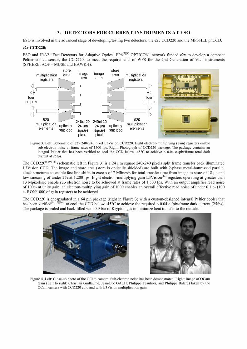
Figure 3. Left: Schematic of e2v 240x240 pixel L3Vision CCD220. Eight electron-multiplying (gain) registers enable
sub electron noise at frame rates of 1500 fps. Right: Photograph of CCD220 package. The package contains an integral Peltier that has been verified to cool the CCD below -45°C to achieve < 0.04 e-/pix/frame total dark current at 25fps.
The CCD220[8][9][11] (schematic left in Figure 3) is a 24 µm square 240x240 pixels split frame transfer back illuminated L3Vision CCD. The image and store area (store is optically shielded) are built with 2-phase metal-buttressed parallel clock structures to enable fast line shifts in excess of 7 Mlines/s for total transfer time from image to store of 18 µs and low smearing of under 2% at 1,200 fps. Eight electron-multiplying gain L3Vision[14] registers operating at greater than 13 Mpixel/sec enable sub electron noise to be achieved at frame rates of 1,500 fps. With an output amplifier read noise of 100e- at unity gain, an electron-multiplying gain of 1000 enables an overall effective read noise of under 0.1 e- (100 e- RON/1000 of gain register) to be achieved.
The CCD220 is encapsulated in a 64 pin package (right in Figure 3) with a custom-designed integral Peltier cooler that has been verified[9][15][16] to cool the CCD below -45°C to achieve the required < 0.04 e-/pix/frame dark current (25fps). The package is sealed and back-filled with 0.9 bar of Krypton gas to minimize heat transfer to the outside.
Figure 4. Left: Close-up photo of the OCam camera. Sub-electron noise has been demonstrated. Right: Image of OCam
team (Left to right: Christian Guillaume, Jean-Luc GACH, Philippe Feautrier, and Philippe Balard) taken by the OCam camera with CCD220 cold and with L3Vision multiplication gain.
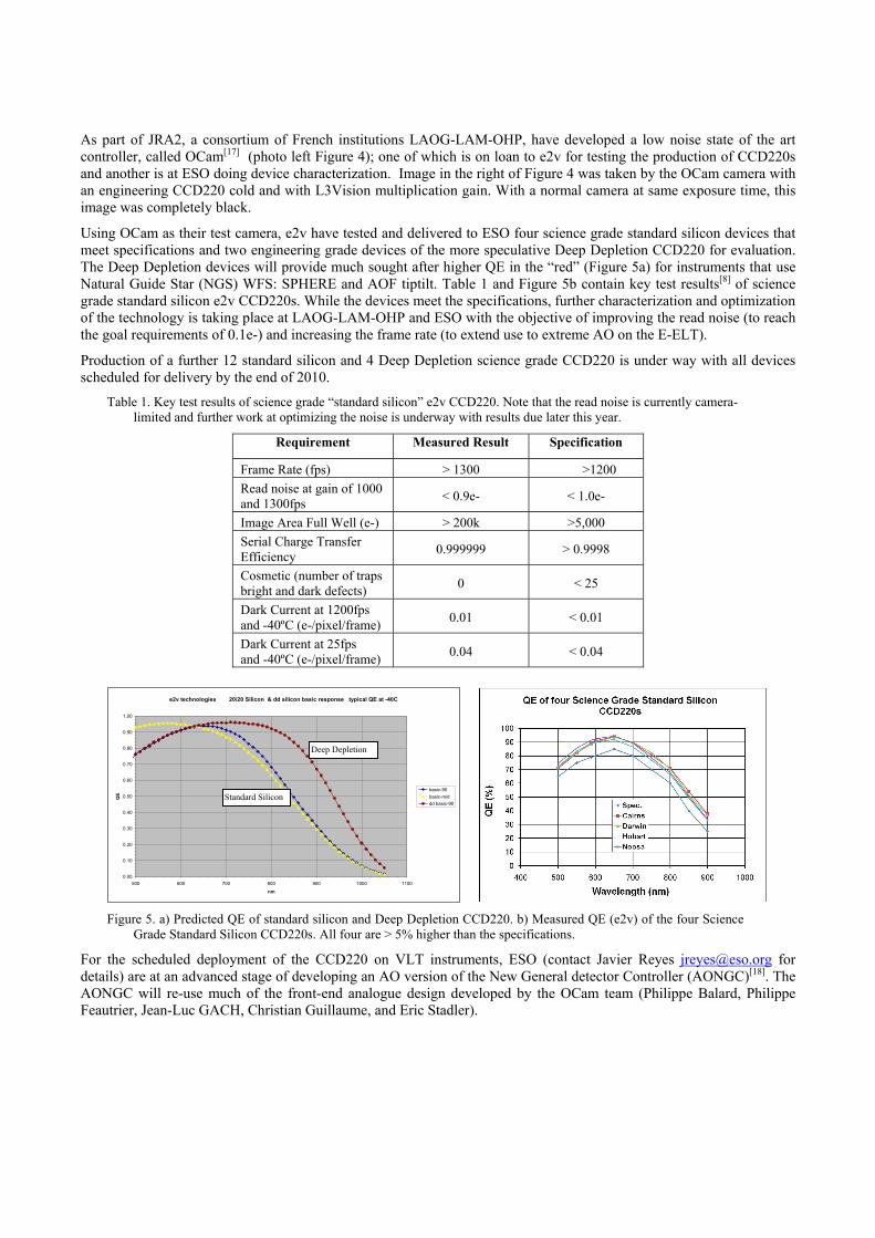
As part of JRA2, a consortium of French institutions LAOG-LAM-OHP, have developed a low noise state of the art controller, called OCam[17] (photo left Figure 4); one of which is on loan to e2v for testing the production of CCD220s and another is at ESO doing device characterization. Image in the right of Figure 4 was taken by the OCam camera with an engineering CCD220 cold and with L3Vision multiplication gain. With a normal camera at same exposure time, this image was completely black.
Using OCam as their test camera, e2v have tested and delivered to ESO four science grade standard silicon devices that meet specifications and two engineering grade devices of the more speculative Deep Depletion CCD220 for evaluation. The Deep Depletion devices will provide much sought after higher QE in the “red” (Figure 5a) for instruments that use Natural Guide Star (NGS) WFS: SPHERE and AOF tiptilt. Table 1 and Figure 5b contain key test results[8] of science grade standard silicon e2v CCD220s. While the devices meet the specifications, further characterization and optimization of the technology is taking place at LAOG-LAM-OHP and ESO with the objective of improving the read noise (to reach the goal requirements of 0.1e-) and increasing the frame rate (to extend use to extreme AO on the E-ELT).
Production of a further 12 standard silicon and 4 Deep Depletion science grade CCD220 is under way with all devices scheduled for delivery by the end of 2010.
Table 1. Key test results of science grade “standard silicon” e2v CCD220. Note that the read noise is currently camera-limited and further work at optimizing the noise is underway with results due later this year.
Requirement Measured Result Specification
Frame Rate (fps) > 1300 >1200 Read noise at gain of 1000 and 1300fps < 0.9e- < 1.0e-
Image Area Full Well (e-) > 200k >5,000 Serial Charge Transfer Efficiency 0.999999 > 0.9998
Cosmetic (number of traps bright and dark defects) 0 < 25
Dark Current at 1200fps and -40ºC (e-/pixel/frame) 0.01 < 0.01
Dark Current at 25fps and -40ºC (e-/pixel/frame) 0.04 < 0.04
Figure 5. a) Predicted QE of standard silicon and Deep Depletion CCD220. b) Measured QE (e2v) of the four Science
Grade Standard Silicon CCD220s. All four are > 5% higher than the specifications.
For the scheduled deployment of the CCD220 on VLT instruments, ESO (contact Javier Reyes [email protected] for details) are at an advanced stage of developing an AO version of the New General detector Controller (AONGC)[18]. The AONGC will re-use much of the front-end analogue design developed by the OCam team (Philippe Balard, Philippe Feautrier, Jean-Luc GACH, Christian Guillaume, and Eric Stadler).
e2v technologies 20/20 Silicon & dd silicon basic response typical QE at -40C
0.00
0.10
0.20
0.30
0.40
0.50
0.60
0.70
0.80
0.90
1.00
500 600 700 800 900 1000 1100
nm
QE
basic-90basic-middd basic-90
Deep Depletion
Standard Silicon
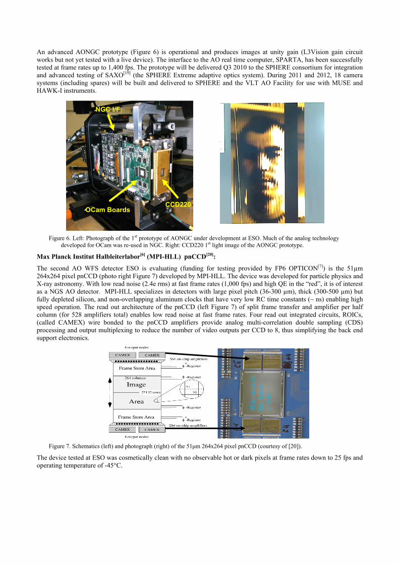
An advanced AONGC prototype (Figure 6) is operational and produces images at unity gain (L3Vision gain circuit works but not yet tested with a live device). The interface to the AO real time computer, SPARTA, has been successfully tested at frame rates up to 1,400 fps. The prototype will be delivered Q3 2010 to the SPHERE consortium for integration and advanced testing of SAXO[19] (the SPHERE Extreme adaptive optics system). During 2011 and 2012, 18 camera systems (including spares) will be built and delivered to SPHERE and the VLT AO Facility for use with MUSE and HAWK-I instruments.
Figure 6. Left: Photograph of the 1st prototype of AONGC under development at ESO. Much of the analog technology
developed for OCam was re-used in NGC. Right: CCD220 1st light image of the AONGC prototype.
Max Planck Institut Halbleiterlabor[6] (MPI-HLL) pnCCD[20]:
The second AO WFS detector ESO is evaluating (funding for testing provided by FP6 OPTICON[7]) is the 51µm 264x264 pixel pnCCD (photo right Figure 7) developed by MPI-HLL. The device was developed for particle physics and X-ray astronomy. With low read noise (2.4e rms) at fast frame rates (1,000 fps) and high QE in the “red”, it is of interest as a NGS AO detector. MPI-HLL specializes in detectors with large pixel pitch (36-300 µm), thick (300-500 µm) but fully depleted silicon, and non-overlapping aluminum clocks that have very low RC time constants (~ ns) enabling high speed operation. The read out architecture of the pnCCD (left Figure 7) of split frame transfer and amplifier per half column (for 528 amplifiers total) enables low read noise at fast frame rates. Four read out integrated circuits, ROICs, (called CAMEX) wire bonded to the pnCCD amplifiers provide analog multi-correlation double sampling (CDS) processing and output multiplexing to reduce the number of video outputs per CCD to 8, thus simplifying the back end support electronics.
Figure 7. Schematics (left) and photograph (right) of the 51μm 264x264 pixel pnCCD (courtesy of [20]).
The device tested at ESO was cosmetically clean with no observable hot or dark pixels at frame rates down to 25 fps and operating temperature of -45°C.
NGC I/F
OCam Boards CCD220
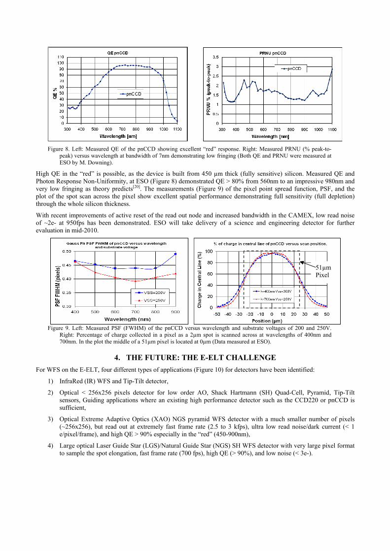
Figure 8. Left: Measured QE of the pnCCD showing excellent “red” response. Right: Measured PRNU (% peak-to-
peak) versus wavelength at bandwidth of 7nm demonstrating low fringing (Both QE and PRNU were measured at ESO by M. Downing).
High QE in the “red” is possible, as the device is built from 450 µm thick (fully sensitive) silicon. Measured QE and Photon Response Non-Uniformity, at ESO (Figure 8) demonstrated QE > 80% from 560nm to an impressive 980nm and very low fringing as theory predicts[20]. The measurements (Figure 9) of the pixel point spread function, PSF, and the plot of the spot scan across the pixel show excellent spatial performance demonstrating full sensitivity (full depletion) through the whole silicon thickness.
With recent improvements of active reset of the read out node and increased bandwidth in the CAMEX, low read noise of ~2e- at 950fps has been demonstrated. ESO will take delivery of a science and engineering detector for further evaluation in mid-2010.
Figure 9. Left: Measured PSF (FWHM) of the pnCCD versus wavelength and substrate voltages of 200 and 250V.
Right: Percentage of charge collected in a pixel as a 2µm spot is scanned across at wavelengths of 400nm and 700nm. In the plot the middle of a 51µm pixel is located at 0µm (Data measured at ESO).
51µm Pixel
4. THE FUTURE: THE E-ELT CHALLENGE For WFS on the E-ELT, four different types of applications (Figure 10) for detectors have been identified:
1) InfraRed (IR) WFS and Tip-Tilt detector,
2) Optical < 256x256 pixels detector for low order AO, Shack Hartmann (SH) Quad-Cell, Pyramid, Tip-Tilt sensors, Guiding applications where an existing high performance detector such as the CCD220 or pnCCD is sufficient,
3) Optical Extreme Adaptive Optics (XAO) NGS pyramid WFS detector with a much smaller number of pixels (~256x256), but read out at extremely fast frame rate (2.5 to 3 kfps), ultra low read noise/dark current (< 1 e/pixel/frame), and high QE > 90% especially in the “red” (450-900nm),
4) Large optical Laser Guide Star (LGS)/Natural Guide Star (NGS) SH WFS detector with very large pixel format to sample the spot elongation, fast frame rate (700 fps), high QE (> 90%), and low noise (< 3e-).
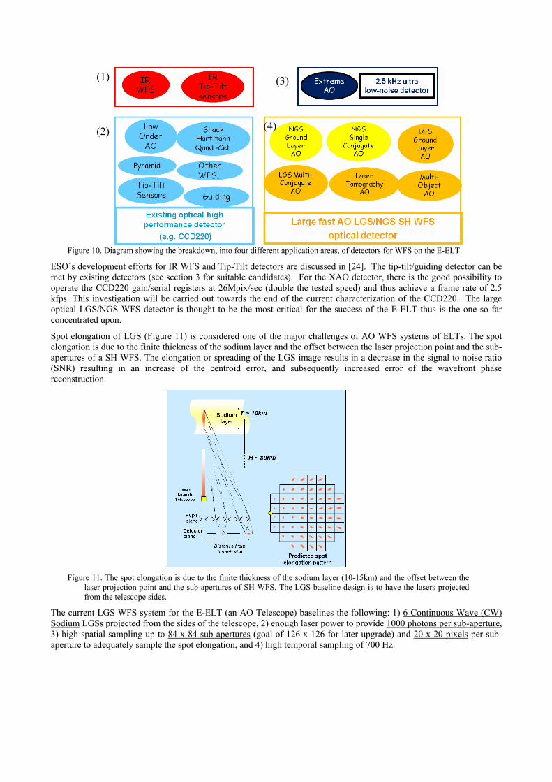
Figure 10. Diagram showing the breakdown, into four different application areas, of detectors for WFS on the E-ELT.
ESO’s development efforts for IR WFS and Tip-Tilt detectors are discussed in [24]. The tip-tilt/guiding detector can be met by existing detectors (see section 3 for suitable candidates). For the XAO detector, there is the good possibility to operate the CCD220 gain/serial registers at 26Mpix/sec (double the tested speed) and thus achieve a frame rate of 2.5 kfps. This investigation will be carried out towards the end of the current characterization of the CCD220. The large optical LGS/NGS WFS detector is thought to be the most critical for the success of the E-ELT thus is the one so far concentrated upon.
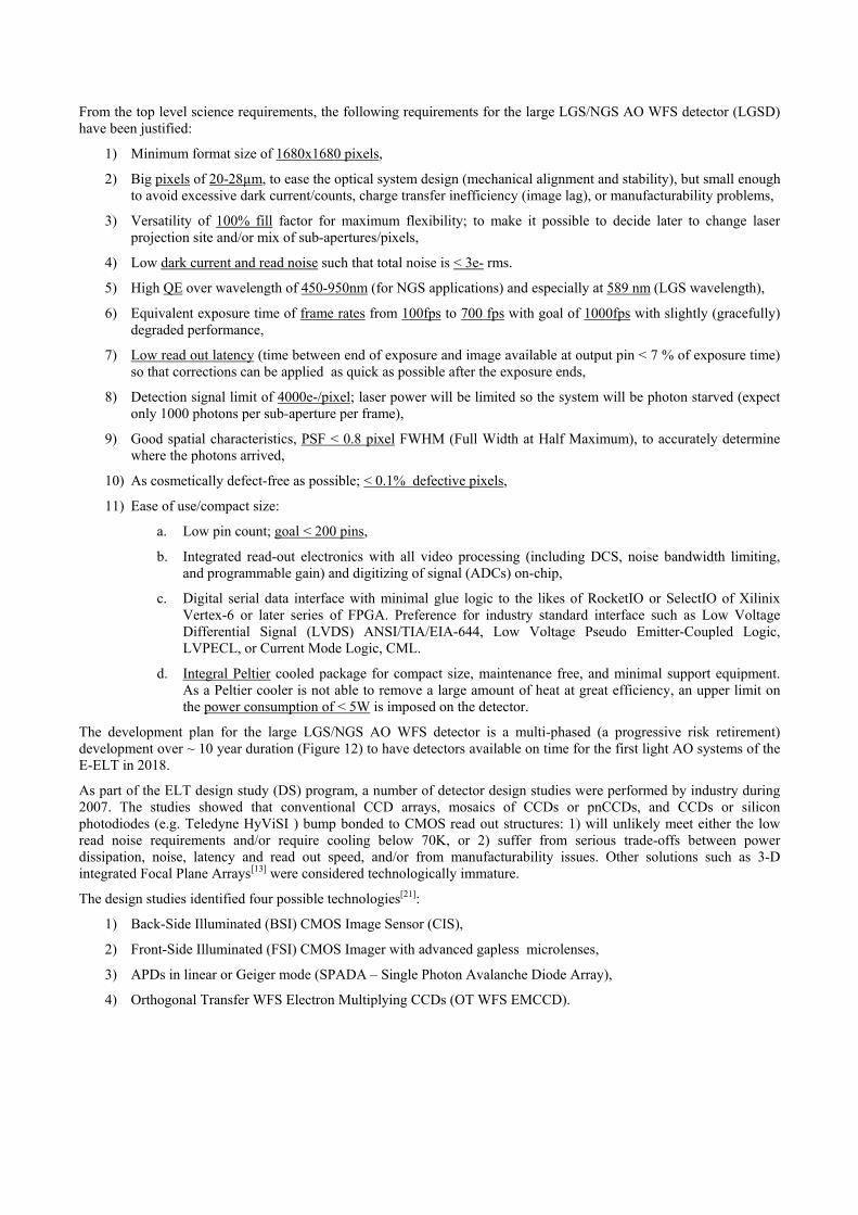
Spot elongation of LGS (Figure 11) is considered one of the major challenges of AO WFS systems of ELTs. The spot elongation is due to the finite thickness of the sodium layer and the offset between the laser projection point and the sub-apertures of a SH WFS. The elongation or spreading of the LGS image results in a decrease in the signal to noise ratio (SNR) resulting in an increase of the centroid error, and subsequently increased error of the wavefront phase reconstruction.
(4)
(3) (1)
(2)
Figure 11. The spot elongation is due to the finite thickness of the sodium layer (10-15km) and the offset between the laser projection point and the sub-apertures of SH WFS. The LGS baseline design is to have the lasers projected from the telescope sides.
The current LGS WFS system for the E-ELT (an AO Telescope) baselines the following: 1) 6 Continuous Wave (CW) Sodium LGSs projected from the sides of the telescope, 2) enough laser power to provide 1000 photons per sub-aperture, 3) high spatial sampling up to 84 x 84 sub-apertures (goal of 126 x 126 for later upgrade) and 20 x 20 pixels per sub-aperture to adequately sample the spot elongation, and 4) high temporal sampling of 700 Hz.
From the top level science requirements, the following requirements for the large LGS/NGS AO WFS detector (LGSD) have been justified:
1) Minimum format size of 1680x1680 pixels,
2) Big pixels of 20-28µm, to ease the optical system design (mechanical alignment and stability), but small enough to avoid excessive dark current/counts, charge transfer inefficiency (image lag), or manufacturability problems,
3) Versatility of 100% fill factor for maximum flexibility; to make it possible to decide later to change laser projection site and/or mix of sub-apertures/pixels,
4) Low dark current and read noise such that total noise is < 3e- rms.
5) High QE over wavelength of 450-950nm (for NGS applications) and especially at 589 nm (LGS wavelength),
6) Equivalent exposure time of frame rates from 100fps to 700 fps with goal of 1000fps with slightly (gracefully) degraded performance,
7) Low read out latency (time between end of exposure and image available at output pin < 7 % of exposure time) so that corrections can be applied as quick as possible after the exposure ends,
8) Detection signal limit of 4000e-/pixel; laser power will be limited so the system will be photon starved (expect only 1000 photons per sub-aperture per frame),
9) Good spatial characteristics, PSF < 0.8 pixel FWHM (Full Width at Half Maximum), to accurately determine where the photons arrived,
10) As cosmetically defect-free as possible; < 0.1% defective pixels,
11) Ease of use/compact size:
a. Low pin count; goal < 200 pins,
b. Integrated read-out electronics with all video processing (including DCS, noise bandwidth limiting, and programmable gain) and digitizing of signal (ADCs) on-chip,
c. Digital serial data interface with minimal glue logic to the likes of RocketIO or SelectIO of Xilinix Vertex-6 or later series of FPGA. Preference for industry standard interface such as Low Voltage Differential Signal (LVDS) ANSI/TIA/EIA-644, Low Voltage Pseudo Emitter-Coupled Logic, LVPECL, or Current Mode Logic, CML.
d. Integral Peltier cooled package for compact size, maintenance free, and minimal support equipment. As a Peltier cooler is not able to remove a large amount of heat at great efficiency, an upper limit on the power consumption of < 5W is imposed on the detector.
The development plan for the large LGS/NGS AO WFS detector is a multi-phased (a progressive risk retirement) development over ~ 10 year duration (Figure 12) to have detectors available on time for the first light AO systems of the E-ELT in 2018.
As part of the ELT design study (DS) program, a number of detector design studies were performed by industry during 2007. The studies showed that conventional CCD arrays, mosaics of CCDs or pnCCDs, and CCDs or silicon photodiodes (e.g. Teledyne HyViSI ) bump bonded to CMOS read out structures: 1) will unlikely meet either the low read noise requirements and/or require cooling below 70K, or 2) suffer from serious trade-offs between power dissipation, noise, latency and read out speed, and/or from manufacturability issues. Other solutions such as 3-D integrated Focal Plane Arrays[13] were considered technologically immature.
The design studies identified four possible technologies[21]:
1) Back-Side Illuminated (BSI) CMOS Image Sensor (CIS),
2) Front-Side Illuminated (FSI) CMOS Imager with advanced gapless microlenses,
3) APDs in linear or Geiger mode (SPADA – Single Photon Avalanche Diode Array),
4) Orthogonal Transfer WFS Electron Multiplying CCDs (OT WFS EMCCD).
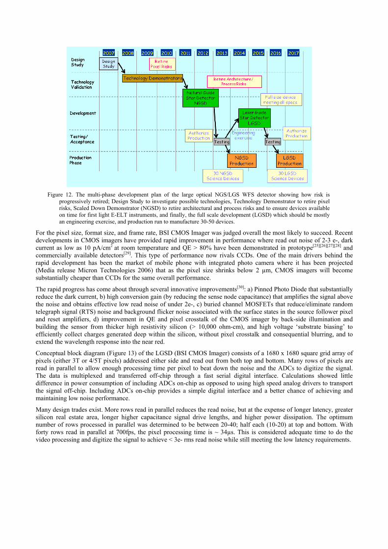
Figure 12. The multi-phase development plan of the large optical NGS/LGS WFS detector showing how risk is
progressively retired; Design Study to investigate possible technologies, Technology Demonstrator to retire pixel risks, Scaled Down Demonstrator (NGSD) to retire architectural and process risks and to ensure devices available on time for first light E-ELT instruments, and finally, the full scale development (LGSD) which should be mostly an engineering exercise, and production run to manufacture 30-50 devices.
For the pixel size, format size, and frame rate, BSI CMOS Imager was judged overall the most likely to succeed. Recent developments in CMOS imagers have provided rapid improvement in performance where read out noise of 2-3 e-, dark current as low as 10 pA/cm2
at room temperature and QE > 80% have been demonstrated in prototype[25][26][27][28] and commercially available detectors[29]. This type of performance now rivals CCDs. One of the main drivers behind the rapid development has been the market of mobile phone with integrated photo camera where it has been projected (Media release Micron Technologies 2006) that as the pixel size shrinks below 2 µm, CMOS imagers will become substantially cheaper than CCDs for the same overall performance.
The rapid progress has come about through several innovative improvements[30]: a) Pinned Photo Diode that substantially reduce the dark current, b) high conversion gain (by reducing the sense node capacitance) that amplifies the signal above the noise and obtains effective low read noise of under 2e-, c) buried channel MOSFETs that reduce/eliminate random telegraph signal (RTS) noise and background flicker noise associated with the surface states in the source follower pixel and reset amplifiers, d) improvement in QE and pixel crosstalk of the CMOS imager by back-side illumination and building the sensor from thicker high resistivity silicon (> 10,000 ohm-cm), and high voltage ‘substrate biasing’ to efficiently collect charges generated deep within the silicon, without pixel crosstalk and consequential blurring, and to extend the wavelength response into the near red.
Conceptual block diagram (Figure 13) of the LGSD (BSI CMOS Imager) consists of a 1680 x 1680 square grid array of pixels (either 3T or 4/5T pixels) addressed either side and read out from both top and bottom. Many rows of pixels are read in parallel to allow enough processing time per pixel to beat down the noise and the ADCs to digitize the signal. The data is multiplexed and transferred off-chip through a fast serial digital interface. Calculations showed little difference in power consumption of including ADCs on-chip as opposed to using high speed analog drivers to transport the signal off-chip. Including ADCs on-chip provides a simple digital interface and a better chance of achieving and maintaining low noise performance.
Many design trades exist. More rows read in parallel reduces the read noise, but at the expense of longer latency, greater silicon real estate area, longer higher capacitance signal drive lengths, and higher power dissipation. The optimum number of rows processed in parallel was determined to be between 20-40; half each (10-20) at top and bottom. With forty rows read in parallel at 700fps, the pixel processing time is ~ 34µs. This is considered adequate time to do the video processing and digitize the signal to achieve < 3e- rms read noise while still meeting the low latency requirements.
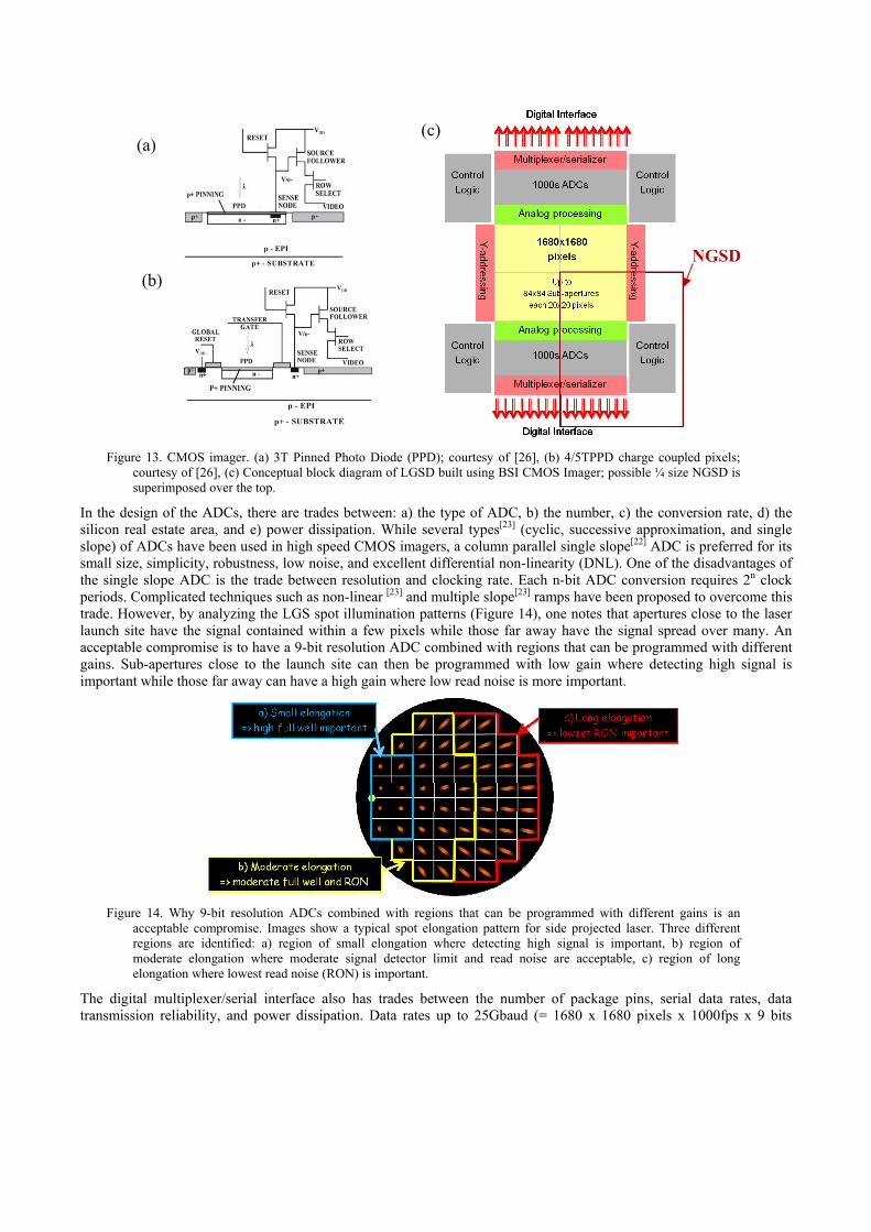
Figure 13. CMOS imager. (a) 3T Pinned Photo Diode (PPD); courtesy of [26], (b) 4/5TPPD charge coupled pixels;
courtesy of [26], (c) Conceptual block diagram of LGSD built using BSI CMOS Imager; possible ¼ size NGSD is superimposed over the top.
In the design of the ADCs, there are trades between: a) the type of ADC, b) the number, c) the conversion rate, d) the silicon real estate area, and e) power dissipation. While several types[23] (cyclic, successive approximation, and single slope) of ADCs have been used in high speed CMOS imagers, a column parallel single slope[22] ADC is preferred for its small size, simplicity, robustness, low noise, and excellent differential non-linearity (DNL). One of the disadvantages of the single slope ADC is the trade between resolution and clocking rate. Each n-bit ADC conversion requires 2n clock periods. Complicated techniques such as non-linear [23] and multiple slope[23] ramps have been proposed to overcome this trade. However, by analyzing the LGS spot illumination patterns (Figure 14), one notes that apertures close to the laser launch site have the signal contained within a few pixels while those far away have the signal spread over many. An acceptable compromise is to have a 9-bit resolution ADC combined with regions that can be programmed with different gains. Sub-apertures close to the launch site can then be programmed with low gain where detecting high signal is important while those far away can have a high gain where low read noise is more important.
(c)
NGSD
(a)
(b)
Figure 14. Why 9-bit resolution ADCs combined with regions that can be programmed with different gains is an
acceptable compromise. Images show a typical spot elongation pattern for side projected laser. Three different regions are identified: a) region of small elongation where detecting high signal is important, b) region of moderate elongation where moderate signal detector limit and read noise are acceptable, c) region of long elongation where lowest read noise (RON) is important.
The digital multiplexer/serial interface also has trades between the number of package pins, serial data rates, data transmission reliability, and power dissipation. Data rates up to 25Gbaud (= 1680 x 1680 pixels x 1000fps x 9 bits
conversion) are required. An example of a possible trade is to use simple (no coding) serial LVDS operating at 220MBaud. This design will require 230 pins [= (25Gbaud / 220MBaud) *2 for differential signaling]. If the operating speed of the LVDS lines is increased to say 400MBaud, then only 128 pins are required. The optimum trade including consideration of other parameters as data reliability and power dissipation will be studied over the next year.
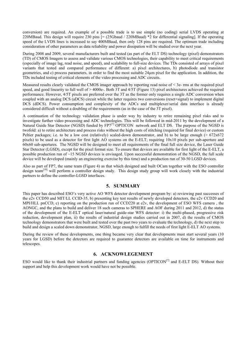
During 2008 and 2009, several manufacturers built and tested (as part of the ELT DS) technology (pixel) demonstrators (TD) of CMOS Imagers to assess and validate various CMOS technologies, their capability to meet critical requirements (especially of image lag, read noise, and speed), and scalability to full-size devices. The TDs consisted of arrays of pixel variants that tested and compared performance of different: a) pixel architectures, b) photodiode and transistor geometries, and c) process parameters, in order to find the most suitable 24µm pixel for the application. In addition, the TDs included testing of critical elements of the video processing and ADC circuits.
Measured results clearly validated the CMOS imager approach by reporting read noise of < 3e- rms at the required pixel speed, and good linearity to full well of > 4000e-. Both 3T and 4/5T (Figure 13) pixel architectures achieved the required performance. However, 4/5T pixels are preferred over the 3T as the former only requires a single ADC conversion when coupled with an analog DCS (aDCS) circuit while the latter requires two conversions (reset+signal) to implement digital DCS (dDCS). Power consumption and complexity of the ADCs and multiplexer/serial data interface is already considered difficult without a doubling of the requirements (as in the case of the 3T pixel).
A continuation of the technology validation phase is under way by industry to retire remaining pixel risks and to investigate further video processing and ADC technologies. This will be followed in mid-2011 by the development of a Natural Guide Star Detector (NGSD) funded by FP7[7] OPTICON network and ELT DS. The purpose of the NGSD is twofold: a) to retire architecture and process risks without the high costs of stitching (required for final device) or custom Peltier packages; i.e. to be a low cost (relatively) scaled-down demonstrator, and b) to be large enough (> 672x672 pixels) to be used as a detector for first light AO systems on the E-ELT; requiring 10x10 pixels per sub-aperture and 60x60 sub-apertures. The NGSD will be designed to meet all requirements of the final full size device, the Laser Guide Star Detector (LGSD), except for the pixel format size. To ensure that devices are available for first light of the E-ELT, a possible production run of ~15 NGSD devices is envisaged. Upon successful demonstration of the NGSD, the full scale device will be developed (mainly an engineering exercise by this time) and a production run of 30-50 LGSD devices.
Also as part of FP7, the same team (Figure 4) as that which designed and built OCam together with the ESO controller design team[18] will perform a controller design study. This design study group will work closely with the industrial partners to define the controller-LGSD interfaces.
5. SUMMARY This paper has described ESO’s very active AO WFS detector development program by: a) reviewing past successes of the e2v CCD50 and MIT/LL CCID-35, b) presenting key test results of newly developed detectors, the e2v CCD20 and MPI/HLL pnCCD, c) reporting on the production run of CCD220 at e2v, the development of ESO WFS camera , the AONGC, and the plans to build and deliver 18 such cameras to SPHERE and AOF during 2011 and 2012, d) the status of the development of the E-ELT optical laser/natural guide-star WFS detector: i) the multi-phased, progressive risk reduction, development plan, ii) the results of industrial design studies carried out in 2007, d) the results of CMOS technology demonstrators that were built and tested over the past two years to evaluate the technology, d) the next step to build and design a scaled down demonstrator, NGSD, large enough to fulfill the needs of first light E-ELT AO systems.
During the review of these developments, one thing became very clear that developments must start several years (10 years for LGSD) before the detectors are required to guarantee detectors are available on time for instruments and telescopes.
6. ACKNOWLEGEMENT ESO would like to thank their industrial partners and funding agencies (OPTICON[7] and E-ELT DS). Without their support and help this development work would have not be possible.

REFERENCES
[1] e2v – e2v technologies, http://www.e2v.com. [2] MIT/LL - MIT Lincoln Laboratory, http://www.ll.mit.edu. [3] Beletic, J., Dorn R., et. al., “A new CCD designed for curvature wavefront sensing”, Optical Detectors for
Astronomy II, Kluwer Academic Publishers (2000).. [4] Dorn, R., “A CCD based curvature wavefront sensor for Adaptive Optics in Astronomy”, Ph.D. thesis,
University of Heidelberg, Germany (2001). [5] Barilet M. et. al., "Flyeyes: final integration and on-sky tests with CFHT's PUEO AO system", Proc. SPIE
7015-193, Marseille (2008). [6] MPI-HLL – Max Planck Institut Halbleiterlabor, http://www.hll.mpg.de. [7] Davies, J., http://www.astro-opticon.org/ [8] Feautrier, P., et. al., “Zero noise wavefront sensor development within the Opticon European network”,
Scientific Detectors for Astronomy, 315-320 (2005). [9] Feautrier, P., et. al., “OCam and CCD220: world's fastest and most sensitive camera system for advanced AO
wavefront sensing”, DfA Garching (2009). [10] Feautrier, P., et. al., “OCam and CCD220: world's fastest and most sensitive camera system for advanced AO
wavefront sensing”, Proc. SPIE 7736-34, San Diego (2010). [11] Downing, M., et. al., “A Dedicated L3Vision CCD for Adaptive Optics Applications”, Scientific Detectors for
Astronomy, 321-328 (2005). [12] Downing, M., et. al., “Custom CCD for adaptive optics applications”, Proc. SPIE 6276-19, Orlando (2006). [13] Suntharalingam, V., et. Al. “Advanced Imager Technology Development at MIT Lincoln Laboratory”, DfA
Garching (2009). [14] Jerram, P., Pool, P. J., et. al., “The LLCCD: low-light imaging without the need for an intensifier”, Proc. SPIE
4306, 178-186 (2001). [15] Feautrier, P., et. al., “Thermal modeling of cooled instrument: from the WIRCam IR camera to CCD Peltier
packages”, Proc. SPIE 6271-41, Orlando (2006). [16] Feautrier, P., et. al., “ESO AO Wavefront Sensor Camera”, DfA, Garching (2009). [17] Gach, J-L., et. al., “A dedicated controller for Adaptive Optics L3CCD developments”, Scientific Detectors for
Astronomy, 639-644 (2005). [18] Reyes, J., et. al., “ESO AO Wavefront Sensor Camera”, DfA, Garching (2009). [19] http://www.eso.org/sci/facilities/develop/instruments/sphere/ [20] Hartmann, R., et. al., “Results of a pnCCD detector system for high-speed optical imaging”, Proc. SPIE 7015-
194, Marseille (2008). [21] Downing, M., et. al., “Detectors for AO wavefront sensing”, Proc. SPIE 70151R-70151R-18, (2008). [22] Albert J.P. Theuwissen : “CMOS Image Sensors : State-of-the-art”, Solid-State Electronics, Vol. 52, pp. 1401-
1406 (2008). [23] Martijn Snoeij, Albert Theuwissen, Johan Huijsing and Kofi Makinwa : “Power and Area Efficient Column-
Parallel ADC Architectures for CMOS Image Sensors”, Invited talk at the 4th Fraunhofer CMOS Image Sensor Workshop, May 6-7, Duisburg (2008).
[24] Finger, G., “Development of high-speed, low-noise NIR HgCdTe avalanche photodiode arrays for adaptive optics and interferometry”, Paper 7742-57 San Diego, (2010).
[25] Janesick, J., Andrews, J., and Elliot, T., “Fundamental performance differences between CMOS and CCD imagers: Part I,” Proc. SPIE 6276, 62760M (2006).
[26] Janesick, J., et. al., “Fundamental performance differences between CMOS and CCD imagers Part II”, Proc. SPIE 6690-03, (2007).
[27] Janesick, J., et. al., “Fundamental performance differences between CMOS and CCD imagers Part III”, Proc. SPIE, San Diego 7439 (2009).
[28] Janesick , J., Cheng, J., Bishop, J., Andrews, J., Tower, J., Walker, J., Grygon, M., and Elliot, T., “CMOS minimal array”, Proc. SPIE 6295, 62950O.1-62950O.15 (2006).
[29] Scientific CMOS (sCMOS), http://www.scmos.com/. [30] Downing, M., et. al., “Review of AO Wavefront Sensing Detectors”, DfA Garching (2009),
http://www.eso.org/sci/meetings/dfa2009/Writeups/WR-Downing_A0WFS_DfA2009.pdf.