ANNUAL REPORT 2007 - University of Illinois at Urbana...
44
ANNUAL REPORT 2007 Meeting date: June 12, 2007 Michael K. Okelman & Brian G. Thomas Department of Mechanical & Industrial Engineering University of Illinois at Urbana-Champaign Design & Installation of Novel Sensors into the Continuous Casting Mold University of Illinois at Urbana-Champaign • Metals Processing Simulation Lab • Michael K. Okelman 2 Acknowledgements • Continuous Casting Consortium Members • National Science Foundation – DMI 04-23794 (Strip); – DMI 05-28668 (Sensor); GOALI DMI 05-00453 (Online) • M. Powers & Sumitec Siemens VAI Services • C. Gulyash, K. Parrish, & MEL Machine Shop • J. Soares & Center for Microanalysis of Materials at Frederick Seitz Materials Research Laboratory • H. Mojal & STAPLA Ultrasonics Corporation • S. Fiegle & Mittal Steel - Riverdale • Other Graduate students
Transcript of ANNUAL REPORT 2007 - University of Illinois at Urbana...

ANNUAL REPORT 2007Meeting date: June 12, 2007
Michael K. Okelman& Brian G. Thomas
Department of Mechanical & Industrial EngineeringUniversity of Illinois at Urbana-Champaign
Design & Installation of Novel Sensors into the Continuous Casting Mold
University of Illinois at Urbana-Champaign • Metals Processing Simulation Lab • Michael K. Okelman 2
Acknowledgements• Continuous Casting Consortium Members• National Science Foundation
– DMI 04-23794 (Strip);
– DMI 05-28668 (Sensor); GOALI DMI 05-00453 (Online)
• M. Powers & Sumitec Siemens VAI Services• C. Gulyash, K. Parrish, & MEL Machine Shop• J. Soares & Center for Microanalysis of Materials at
Frederick Seitz Materials Research Laboratory• H. Mojal & STAPLA Ultrasonics Corporation• S. Fiegle & Mittal Steel - Riverdale• Other Graduate students

University of Illinois at Urbana-Champaign • Metals Processing Simulation Lab • Michael K. Okelman 3
Embedded Mold Temperature Sensor
• Coordinate design, manufacturing, testing, & implementation of sensor strip into CC mold between UIUC, UW - Madison, Sumitec, MittalSteel - Riverdale, & Nucor
• Sensor description, installation, & design• Methods to attach sensor
– hang & plate– silver paste– ultrasonic welding
• Plating trials• Air gap geometry effect on heat transfer
University of Illinois at Urbana-Champaign • Metals Processing Simulation Lab • Michael K. Okelman 4
The Continuous Casting Mold
(images courtesy Brian Thomas, personal communication)

University of Illinois at Urbana-Champaign • Metals Processing Simulation Lab • Michael K. Okelman 5
Schematic of Initial Solidification
Contact Resistances
Molten Steel Pool
Solidifying Steel ShellOscillation Mark
Copper Mold
Liquid Flux
Air Gap
Flux Powder
Flux Rim
Meniscus
Steel surface level
Solidified Flux
Liquid flux film(low friction)
Solid flux film(high friction)
What’s the temperature behavior in this region?
(images courtesy Brian Thomas, personal communication)
University of Illinois at Urbana-Champaign • Metals Processing Simulation Lab • Michael K. Okelman 6
Installation of Sensor Strip into Continuous Casting Mold
150mm
mold top
water slot
meniscus
conventional embedded thermocouple
Copper mold
2.0 x 0.1 mm sensor strip
cross-section view through meniscus
sensor
0.3mm Nickel plating
3D View
wire bundle
12mm
140mm
x
y
z
y
x
wireless transmitter
(images courtesy Brian Thomas, personal communication)

University of Illinois at Urbana-Champaign • Metals Processing Simulation Lab • Michael K. Okelman 7
Prediction of Longitudinal Cracks by Interpreting Thermocouple Signals
D. Stewart, P.N. Hewitt and L. Peeters: "The Prediction of Longitudinal Cracking During Slab Casting", in Steelmaking Conference Proceedings, vol. 79, ISS, Warrendale, PA, Pittsburgh, PA, 1996, pp. 207-214.
Analysis system developed by British Steel, Sidmar, and CRM
MTM System
Instrumented mold
Juntion Box
Spray Chamber Compensating Cables
Thermocouple Data
Acquisition Cubicle
Plant Signals Data
Acquisition Cubicle
high-speed serial networkComputer
(interpretation of signals)
Control-room Operator Display
University of Illinois at Urbana-Champaign • Metals Processing Simulation Lab • Michael K. Okelman 8
Wireless Thermocouple System
• MicroStrain 2.4 GHz TC-Link– Combines full thermocouple conditioning
with wireless system
– Supports simultaneous data transmission from multiple sensors
– Sample rates from 1 sample/minute to 5 samples/second
– Communication range up to 70 m
– Base station transceiver displays & logs data; single host transceiver can address thousands of sensor nodes
Supports type J K R S T E

University of Illinois at Urbana-Champaign • Metals Processing Simulation Lab • Michael K. Okelman 9
MicroStrain TC-Link
University of Illinois at Urbana-Champaign • Metals Processing Simulation Lab • Michael K. Okelman 10
Wireless Apparatus & Experiment
• TC Link attached to Type K thermocouple
• Thermocouple submerged in RT water
• Thermometer used to validate TC Link measurement
• TC Link receiver and laptop within caster pulpit
• Apparatus position and EMBr current varied

University of Illinois at Urbana-Champaign • Metals Processing Simulation Lab • Michael K. Okelman 11
Validation of TC Link
0
5
10
15
20
25
30
09:50:24 10:04:48 10:19:12 10:33:36 10:48:00 11:02:24 11:16:48
time
tem
pe
ratu
re (
Ce
lciu
s)
TC Link temperature
thermometer temperature
Apparatus located away from mold, but still on cast floor. No EMBr.
University of Illinois at Urbana-Champaign • Metals Processing Simulation Lab • Michael K. Okelman 12
Validation of TC Link under EM Field
15
16
17
18
19
20
21
22
23
24
25
11:19:41 11:22:34 11:25:26 11:28:19 11:31:12 11:34:05 11:36:58 11:39:50 11:42:43 11:45:36 11:48:29
time
tem
per
atu
re (
Cel
ciu
s)
TC Link temperature
EMBr @ 150 A
(turned off, then on) TC Link moved to WF
EMBr @ 250 A
(TC Link located @ NF)

University of Illinois at Urbana-Champaign • Metals Processing Simulation Lab • Michael K. Okelman 13
Proposed Positioning & Plating of Sensor on Cu Narrow Face
narrow face cover
silicone protective layer over pad
(must not damage sensor pad!)
sensor pad protruding from sensor strip (connection sites on reverse side of pad)
prior to acid treatment & plating after acid treatment & plating
sensor pad
sensor strip
Cu narrow face
3D view front view
University of Illinois at Urbana-Champaign • Metals Processing Simulation Lab • Michael K. Okelman 14
Sensor Design
thermopile (sensor array)
chromel-alumel TC junctions (13 in series)
line width / spacing width = 15 µm
130 mm
2 mm
10 mm
40 mm
sensor pad
ceramic layer (for heat flux
measurement)
University of Illinois at Urbana-Champaign • Metals Processing Simulation Lab • Michael K. Okelman 15
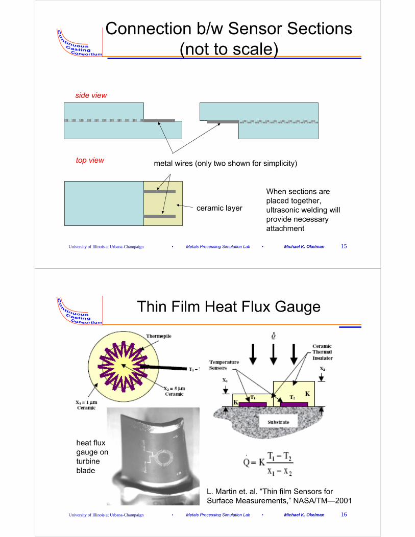
Connection b/w Sensor Sections (not to scale)
side view
top view metal wires (only two shown for simplicity)
ceramic layer
When sections are placed together, ultrasonic welding will provide necessary attachment
University of Illinois at Urbana-Champaign • Metals Processing Simulation Lab • Michael K. Okelman 16
Thin Film Heat Flux Gauge
L. Martin et. al. “Thin film Sensors for Surface Measurements,” NASA/TM—2001
heat flux gauge on turbine blade

University of Illinois at Urbana-Champaign • Metals Processing Simulation Lab • Michael K. Okelman 17
High temp FBG Sensor
• Model number OETMS-700
• Range -50°C to 700°C• Resolution of 1.0°C• Precision of +/- 2.0°C
• Packaged with SS tubing to withstand high temperature• Standard FC/PC connector used for easy plug in connection
with light source and FBG sensor interrogator
University of Illinois at Urbana-Champaign • Metals Processing Simulation Lab • Michael K. Okelman 18
Advantages of FBG Sensors
• Real-time monitoring at critical locations not accessible to ordinary sensors
• Embedded sensors are protected from damage caused by environmental effects
• Dominant technology are fiber optic sensors which offer light weight, immunity to electromagnetic interference, non-obtrusive embeddability, resistance to hostile environments, & high bandwidth capability
• Gratings, now commercial available, have been considered suitable for measuring static and dynamic fields, such as temperature and strain
from “Metal Embedded Fiber Bragg Grating Sensors in Layered Manufacturing” X. Li, F. Prinz

University of Illinois at Urbana-Champaign • Metals Processing Simulation Lab • Michael K. Okelman 19
Custom OETMS-700 for UIUC
• Last 50mm nickel plated to assist plating in Ni layer of Cu mold
• Sensor is approximately 10mm in length
10 mm
50 mm
nickel plated
cable total length = 1 m
to interrogator
sensor
diameter < 250 µm
circular cross-section
diameter < 150 µm
University of Illinois at Urbana-Champaign • Metals Processing Simulation Lab • Michael K. Okelman 20
Interrogator Systems
• 3 different systems exist from O/E Land– Low cost– High speed– Standard
• Systems differ regarding– Number of sensors monitored– Number of sensors per channel– Speed of transmission– Accuracy of transmission– Price
• Overview of low cost system is provided as an example

University of Illinois at Urbana-Champaign • Metals Processing Simulation Lab • Michael K. Okelman 21
Inter-FBG (Low Cost)
University of Illinois at Urbana-Champaign • Metals Processing Simulation Lab • Michael K. Okelman 22
Questions & Concerns• Can a length of fiber optic cable have two sensors in it,
or is a separate cable necessary?– Yes, a length of fiber optic cable can have two sensors in it, or
more than two. No need for a separate cable.
• If it is possible to have more than one sensor per fiber optic cable, is the diameter of the cable increased?– In the case of more than two sensors in one fiber optic cable, the
diameter of the cable will not increase as the sensors will be located at different positions in the fiber optic cable.
• How are temperature and strain effects decoupled by the interrogator?– The temperature and strain effects are decoupled by the sensor
wavelength change.
• If I embed the sensor in a metal part, will the interrogator be able to tell me the temperature, strain, or both?– The interrogator will tell you both of them: the temperature and
the strain.

University of Illinois at Urbana-Champaign • Metals Processing Simulation Lab • Michael K. Okelman 23
Methods to Attach Sensor• Hang sensor over copper & electroplate!• Silver paste
– bakes in 2 hours– electrically & thermally conductive (k=109 W/m-K)– inorganic– adhesive & coating applications to 1200°F– easy to perform a trial
• Ultrasonic welding– two members subjected to static normal force & oscillating shearing
stresses– no melting and fusion take place– can join dissimilar metals
• Diffusion bonding/welding– joint results from atoms moving across the interface & some plastic
deformation– requires temperatures of about 0.5Tm– parts heated & pressure is applied– suitable for dissimilar metals
University of Illinois at Urbana-Champaign • Metals Processing Simulation Lab • Michael K. Okelman 24
Plating Trial May 2006
• Objectives– Evaluate plating ability to attach sensor to mold
– Quantify efficiency of plating to fill gap
• Trial Procedure1. Mount sensor onto test coupon
2. Mask sensor & hang in tank
3. Nickel electroplate coupon
4. Metallography

University of Illinois at Urbana-Champaign • Metals Processing Simulation Lab • Michael K. Okelman 25
Sumitec Plating Case 1
Case 1• sensor NOT grounded to Cu• plate triangular sensor on Cu• cut cross-sections to look for
air gaps & other bonding issues (performed at UIUC)
top view
Test: How does the width of the strip affect the ability of the Ni atoms to plate under the sensor?
side view
University of Illinois at Urbana-Champaign • Metals Processing Simulation Lab • Michael K. Okelman 26
Sumitec Plating Case 2
Case 2• sensor is grounded
• plate rectangular sensor on Cu
• cut cross-sections to look for air gaps & other bonding issues (performed at UIUC)
side view
Test: How does the strip distance to the Cu affect the ability of the Ni atoms to plate under the sensor?
top view

University of Illinois at Urbana-Champaign • Metals Processing Simulation Lab • Michael K. Okelman 27
Sumitec Plating Cases 1 & 2
Schematic of (a) case 1—variable width trial and (b) case 2—variable gap thickness trial
1.82 mm
(a) (b)
5.64 mm
71.3 mm
0.254 mm
0.940 mm
55.8 mm
1.82 mm
University of Illinois at Urbana-Champaign • Metals Processing Simulation Lab • Michael K. Okelman 28
Hypotheses Regarding Plating Trial in Vertical Plating Tank
sensor strip
“dogleg”
(sensor strip contacts mold and is therefore grounded)
if sensor is grounded…
Ni plating
Cu
Ni plating
Cu
if sensor is NOT grounded…
1 mm
1 mm
side view

University of Illinois at Urbana-Champaign • Metals Processing Simulation Lab • Michael K. Okelman 29
Commercial Plating Trial in Vertical Plating Tank
top view
thickness 0.100 mm
University of Illinois at Urbana-Champaign • Metals Processing Simulation Lab • Michael K. Okelman 30
Electroplating of Coupon
1. The coupon was plated in a standard production rectifier in a nickel sulfamate bath. Area was 4 square inches, required current for 0.001” per hour was 0.75 amps.
2. Pretreat of coupon at the tank consisted of rinse with DI water, followed by acid treatment with 10% solution of sulfamic acid (normal production step). Sensors appeared to suffer no ill effects from this pretreatment, so the process continued. Note: as mentioned previously the sensors were not exposed to nitric acid to ensure the plating trial could continue at this point.
3. Coupon was run at 1.8 volts at a distance of ~6” from the anode which is within normal production limits. Current was set at approximately 1 amp via hand held current measuring device because 1 amp was not enough to be indicated on rectifier control.
4. Part was electroplated for approximately 65 hours.5. Total deposit thickness was 0.082 inches. Theoretical deposit
should have been [ 65 hours x 0.001 inches / hour x 1 amp / .75amps ] = 0.086 inches. In other words this was as expected and no plating abnormalities surfaced due to the small sample size.

University of Illinois at Urbana-Champaign • Metals Processing Simulation Lab • Michael K. Okelman 31
Analyzing the Commercially Plated Copper Coupon
• Did nickel deposit, and at what combination of width & gap?
• Did nickel adhere to the copper, sensor, or both?
• Metallography performed at UIUC
University of Illinois at Urbana-Champaign • Metals Processing Simulation Lab • Michael K. Okelman 32
Metallography Steps
1. Cut plated copper coupon into 8 pieces per Ni strip (16 total samples) with EDM to observe cross-section

University of Illinois at Urbana-Champaign • Metals Processing Simulation Lab • Michael K. Okelman 33
Metallography Steps
2. Mounting: each of 16 samples mounted with epoxy into 1 ¼”specimens
3. Grinding: rough grind with 180, then hand grind 240, 320, 400, 600, then machine fine grind 800 & 1200 grit
University of Illinois at Urbana-Champaign • Metals Processing Simulation Lab • Michael K. Okelman 34
Metallography Steps
4. Polishing: 1 micron & 0.3 micron (when necessary) using short knap cloth & accompanying suspensions

University of Illinois at Urbana-Champaign • Metals Processing Simulation Lab • Michael K. Okelman 35
Metallography Steps
5. Etching: Immerse each sample in 1 part HNO3, 1 part acetic acid (glacial), & 1 part DI water for 15 seconds
University of Illinois at Urbana-Champaign • Metals Processing Simulation Lab • Michael K. Okelman 36
Optical Microscope Pictures
• Optical microscope & image capture software used to take digital pictures of each sample to determine plating under Ni strip

University of Illinois at Urbana-Champaign • Metals Processing Simulation Lab • Michael K. Okelman 37
Plating under Nickel Strip
200 microns
University of Illinois at Urbana-Champaign • Metals Processing Simulation Lab • Michael K. Okelman 38
regions of high current density
Current Density & Plating Rate

University of Illinois at Urbana-Champaign • Metals Processing Simulation Lab • Michael K. Okelman 39
Plating Buildup Animation
University of Illinois at Urbana-Champaign • Metals Processing Simulation Lab • Michael K. Okelman 40
Plating Buildup Animation

University of Illinois at Urbana-Champaign • Metals Processing Simulation Lab • Michael K. Okelman 41
Plating Buildup Animation
University of Illinois at Urbana-Champaign • Metals Processing Simulation Lab • Michael K. Okelman 42
Plating Buildup Animation

University of Illinois at Urbana-Champaign • Metals Processing Simulation Lab • Michael K. Okelman 43
Plating Buildup Animation
University of Illinois at Urbana-Champaign • Metals Processing Simulation Lab • Michael K. Okelman 44
Plating Buildup Animation

University of Illinois at Urbana-Champaign • Metals Processing Simulation Lab • Michael K. Okelman 45
Plating Buildup Animation
University of Illinois at Urbana-Champaign • Metals Processing Simulation Lab • Michael K. Okelman 46
Plating Buildup Animation

University of Illinois at Urbana-Champaign • Metals Processing Simulation Lab • Michael K. Okelman 47
200 microns
Final Geometry
University of Illinois at Urbana-Champaign • Metals Processing Simulation Lab • Michael K. Okelman 48
Drawing Void & Strip Outlines
200 microns

University of Illinois at Urbana-Champaign • Metals Processing Simulation Lab • Michael K. Okelman 49
Air “Void” & Strip Dimensions
200 microns
void width void thickness
Ni strip (outlined)
gap thickness
strip width 200 microns
University of Illinois at Urbana-Champaign • Metals Processing Simulation Lab • Michael K. Okelman 50
Qualitative Analysis of Plating Trial
• After pictures of each sample were taking & void outlined, the following were measured:– void thickness
– void width
– gap thickness
– thickness of plating under Ni strip• above & below void for left, right, & center

University of Illinois at Urbana-Champaign • Metals Processing Simulation Lab • Michael K. Okelman 51
Case 1 (Variable Width Strip)Case 1
0
1000
2000
3000
4000
5000
6000
20000 30000 40000 50000 60000
distance along sample (microns)
(mic
ron
s)
void thicknessvoid widthgap thicknessstrip width
• The strip width decreases as the distance along the sample increases• The void width in all cases is larger than the sensor width due to the notches
at the edges of the void• As the strip width decreases, the void thickness decreases as well
University of Illinois at Urbana-Champaign • Metals Processing Simulation Lab • Michael K. Okelman 52
Case 1 (Variable Width Strip)Case 1
0
50
100
150
200
250
300
350
400
1000 2000 3000 4000 5000 6000
strip width (microns)
pla
tin
g t
hic
knes
s at
cen
ter
(mic
ron
s)
top
bottom
total
• As the strip width increases, the plating thickness at the center decreases since the aspect ratio (defined as strip width to gap thickness at center) is increasing

University of Illinois at Urbana-Champaign • Metals Processing Simulation Lab • Michael K. Okelman 53
Case 2 (Variable Gap Thickness)Case 2
0
500
1000
1500
2000
2500
10000 15000 20000 25000 30000 35000 40000 45000 50000
distance along sample (microns)
(mic
ron
s)
void thicknessvoid widthgap thicknessstrip width
• The distance between the strip & Cu is gradually increased as distance along the sample increases
• The strip width is held constant
University of Illinois at Urbana-Champaign • Metals Processing Simulation Lab • Michael K. Okelman 54
Case 2 (Variable Gap Thickness)Case 2
0
20
40
60
80
100
120
140
160
0 100 200 300 400 500
gap thickness (microns)
pla
tin
g t
hic
knes
s at
cen
ter
(mic
ron
s)
top
bottom
total
• As gap thickness increases, plating thickness at the center increases

University of Illinois at Urbana-Champaign • Metals Processing Simulation Lab • Michael K. Okelman 55
Effect of Aspect Ratio
0
0.1
0.2
0.3
0.4
0.5
0.6
0.7
0.8
0.9
1
0 2 4 6 8 10 12 14 16 18 20
aspect ratio
fra
cti
on
fil
led
at
ce
nte
r
case 2
case 1
Predict 100% filling when aspect ratio ~1
University of Illinois at Urbana-Champaign • Metals Processing Simulation Lab • Michael K. Okelman 56
Plating Trial Conclusions
• Ni adhered well to the top, bottom, & sides of Ni strip, as well as the Cu coupon (in almost all cases)
• However, every sample observed contained an air gap (or “void”) between the Ni strip & Cu coupon
• As Ni strip width decreases, or gap thickness increases, more plating reaches under the strip
• Aspect ratio of the space between the strip and Cu substrate roughly governs the fraction of the gap filled by the plating

University of Illinois at Urbana-Champaign • Metals Processing Simulation Lab • Michael K. Okelman 57
Plating Trial Conclusions (cont’)
• Plating stops (to form interior void) when 2 layers of growing grains impinge just past edge of strip, and restrict access of plating to interior (forming gap)
• Explains why gap is wider than strip (impingement first occurs beyond edge of strip)
• Better coverage could be obtained by curving or rounding strip edge, in order to encourage plating of center first
• Avoiding grounding should allow better coverage (by letting growth occur from plate and go around strip)
• In practice, grounding has negligible effect (likely because sample is always close enough to quickly become effectively grounded)
University of Illinois at Urbana-Champaign • Metals Processing Simulation Lab • Michael K. Okelman 58
Repeat of Aspect Ratio Trials
• 2 new Ni strips will be prepared at UIUC (cut using EDM) to investigate gaps with smaller aspect ratios:– Repeat case 1) Triangular-shaped (0—6.0mm wide x 50mm
long) to be mounted ~1.5mm from Cu coupon, plated while ungrounded (taking care to plate over pointed end)
• Aspect ratios investigated: 0—4 (overlapping previous trial)
– Repeat case 2) Rectangular-shaped (0.5mm wide x 50mm long) strip to be mounted 0—1.5mm from Cu coupon, plated while suspended above coupon (grounded)
• Aspect ratios investigated: 0.33—∞ (divide by zero gap thickness)

University of Illinois at Urbana-Champaign • Metals Processing Simulation Lab • Michael K. Okelman 59
Repeat of Aspect Ratio Trials
Illustration of (a) case 1—variable width trial and (b) case 2—variable gap thickness trial
(a) (b)
6.0 mm
50 mm
1.5 mm 1.5 mm
50 mm
0.5 mm
University of Illinois at Urbana-Champaign • Metals Processing Simulation Lab • Michael K. Okelman 60
Methods to Attach Sensor• Hang sensor over copper & electroplate!• Silver paste
– bakes in 2 hours– electrically & thermally conductive (k=109 W/m-K)– inorganic– adhesive & coating applications to 1200°F– easy to perform a trial
• Ultrasonic welding– two members subjected to static normal force & oscillating shearing
stresses– no melting and fusion take place– can join dissimilar metals
• Diffusion bonding/welding– joint results from atoms moving across the interface & some plastic
deformation– requires temperatures of about 0.5Tm– parts heated & pressure is applied– suitable for dissimilar metals

University of Illinois at Urbana-Champaign • Metals Processing Simulation Lab • Michael K. Okelman 61
Attaching the Sensor with Silver Paste
Since the conductivity of the silver paste is 109 W/mK, method is OK if:
• Needs secure bond between sensor strip and Cu
• Must have no air gaps• Must survive acid
pretreatment steps• Must successfully be nickel
plated at commercial facility
Metallography will be performed at UIUC this summer
sensor
Cu
silver paste
University of Illinois at Urbana-Champaign • Metals Processing Simulation Lab • Michael K. Okelman 62
Silver Paste Spec Sheet
Reference Notes:
-Order 59x-A for adhesive uses, 59x-C for coating uses

University of Illinois at Urbana-Champaign • Metals Processing Simulation Lab • Michael K. Okelman 63
Silver Paste Trials
• Copper coupons with silver pasted nickel strips– Plate over top (same as
previous trial)
– Plating thickness should be ~2mm (same as previous trial)
– Repeat quantitative analysis at UIUC
• Copper block with silver pasted nickel strips (1 messy attachment, 1 clean attachment)– Plate over top (same as previous
trial)
– Plating thickness should be ~2mm
– Machine surface flat to ~1mm, leaving 0.5mm plating over top of Ni strips
– Cut sample in half between strips (one intact strip in each half)
– Flame test (immerse Cu block in water and heat the Ni plating layer)
– Repeat quantitative analysis at UIUC
University of Illinois at Urbana-Champaign • Metals Processing Simulation Lab • Michael K. Okelman 64
“Clean” Silver Paste Trial
• Clean Cu surface & Ni strip with alcohol• Mask Cu surface with black electrical tape• Add layer of reinforced fiberglass tape to
assist silver paste removal• Attach large piece of clear packing tape to Ni
strip to prevent silver paste from adhering to top surface of strip
• Carefully attach strip to Cu surface with silver paste (with thinnest layer possible while maintaining perfect coverage)– glue line should be less than 10 mils (254µm)– “dull” side of strip should be facing up
• Remove tape with unwanted paste

University of Illinois at Urbana-Champaign • Metals Processing Simulation Lab • Michael K. Okelman 65
Plating Trial May 2007
University of Illinois at Urbana-Champaign • Metals Processing Simulation Lab • Michael K. Okelman 66
Upcoming Plating Trial

University of Illinois at Urbana-Champaign • Metals Processing Simulation Lab • Michael K. Okelman 67
Methods to Attach Sensor• Hang sensor over copper & electroplate!• Silver paste
– bakes in 2 hours– electrically & thermally conductive (k=109 W/m-K)– inorganic– adhesive & coating applications to 1200°F– easy to perform a trial
• Ultrasonic welding– two members subjected to static normal force & oscillating shearing
stresses– no melting and fusion take place– can join dissimilar metals
• Diffusion bonding/welding– joint results from atoms moving across the interface & some plastic
deformation– requires temperatures of about 0.5Tm– parts heated & pressure is applied– suitable for dissimilar metals
University of Illinois at Urbana-Champaign • Metals Processing Simulation Lab • Michael K. Okelman 68
Ultrasonically Attached Nickel Strip
Ultrasonic welding trial performed at STAPLA Ultrasonics Corporation with Condor Universal Weld Head
Special thanks to H. Mojal for his assistance

University of Illinois at Urbana-Champaign • Metals Processing Simulation Lab • Michael K. Okelman 69
Ultrasonically Attached Nickel Sensor
University of Illinois at Urbana-Champaign • Metals Processing Simulation Lab • Michael K. Okelman 70
Ultrasonic Welding Conclusions
• In past experiences, ultrasonic welding near, around, or on top of sensors has lead to irreversible damage
• The machining pattern caused by the weld horn on the ultrasonic machine is unavoidable
• Computer modeling the welding process is difficult/impossible; it is better to fabricate the sensor & weld
• To avoid damage, construct a sensor strip with the sensor far away from the weld horn

University of Illinois at Urbana-Champaign • Metals Processing Simulation Lab • Michael K. Okelman 71
Using Simulations to Help Design and Test Sensors
• What are the temperatures & stresses associated with continuous casting coatings?– literature review
– perform heat transfer & thermal stress analysis
• How can the duration of the dip test be determined?– analytical solution regarding steel solidifying in a
thick copper mold
– simulate solidification to determine temperature distribution in copper block
University of Illinois at Urbana-Champaign • Metals Processing Simulation Lab • Michael K. Okelman 72
What is a Dip Test?
• Copper block is partially submerged in molten steel for a determined amount of time
• The most available source of molten steel for a dip test would be a tundish
• Alternative to testing plated sensor in a copper mold during casting
• Do not interrupt the casting process or affect the mold
• Attempt to match the temperatures & stresses encountered in the copper mold of a continuous caster
molten steel
sensor strip

University of Illinois at Urbana-Champaign • Metals Processing Simulation Lab • Michael K. Okelman 73
Material Properties
1.31E-051.77E-05α (/K)
0.310.343v
207110E (GPa)
1007456380Cp (J/kg-K)
0.026370350k (W/m-K)
1.161488908960ρ (kg/m3)
airNiCu
(values from Kabelmetal “Copper and Copper Alloy Mold Liners for Continuous Casting of Steel” and MatWeb.com)
will be used for modeling air gap under sensor
University of Illinois at Urbana-Champaign • Metals Processing Simulation Lab • Michael K. Okelman 74
1D Heat Transfer in Bimetallic Strip
convection: Twater= 25°C, h= 21,000 W/m2-K
q= 2.0E6 W/m2
dT/dn = 0 dT/dn = 0
Boundary Conditions: molten steel contacts the bottom of the test strip and top of the strip is water cooled
∞+⎟⎟⎠
⎞⎜⎜⎝
⎛++= T
hk
t
k
tqT
Cu
Cu
Ni
Nibottom
1thermal resistance method applied to composite wall
copper
nickel
24 mm
1 mm

University of Illinois at Urbana-Champaign • Metals Processing Simulation Lab • Michael K. Okelman 75
Temperature Distribution in Bimetallic Strip
1D temperature distribution– temperatures
higher at Ni coating due to lower thermal conductivity of Ni compared to Cu
Temperature in Kelvin
%difference 6.82E-05
comparison b/w analytical & experimental:
University of Illinois at Urbana-Champaign • Metals Processing Simulation Lab • Michael K. Okelman 76
Embedded Sensor Air Gap Model
• Assuming everything is working smoothly, the complexity of the model can be increased– add air gap at interface incorrect plating procedure
• How does the behavior change?
24 mm
50 mm
50 mm1 mm

University of Illinois at Urbana-Champaign • Metals Processing Simulation Lab • Michael K. Okelman 77
Air Gap Geometry
2 mm
0.1 mmNO ELEMENTS!
University of Illinois at Urbana-Champaign • Metals Processing Simulation Lab • Michael K. Okelman 78
Temperature Distribution
2D temperature distribution near air gap
localized “hot spot”

University of Illinois at Urbana-Champaign • Metals Processing Simulation Lab • Michael K. Okelman 79
Basic Procedure for Indirect Method for Thermal Stress Problems
1) Define & solve thermal problem2) Return to preprocessor & modify the
database– switch element types– specify additional mat’l properties– specify structural BC
3) Read the temperatures from the thermal results file
4) Solve the structural problem
University of Illinois at Urbana-Champaign • Metals Processing Simulation Lab • Michael K. Okelman 80
Thermal Stress of Dip Test (No Air Gap)
Max stresses:
σCu = 67.8 MPa (compression)
σNi = 185 MPa (tension)Cu
Ni coating layer

University of Illinois at Urbana-Champaign • Metals Processing Simulation Lab • Michael K. Okelman 81
Thermal Stress of Dip Test(with 0.1 mm Air Gap)
Max stresses:
σCu = 67.8 MPa (compression)
σNi = 220 MPa (tension)
presence of air gap increases stress by ~19%
Cu
Ni coating layerair gap/sensor
University of Illinois at Urbana-Champaign • Metals Processing Simulation Lab • Michael K. Okelman 82
Air Gap Geometry
gap centerline
gap edge
far from gap
10.9 0
width
thickness

University of Illinois at Urbana-Champaign • Metals Processing Simulation Lab • Michael K. Okelman 83
Original Geometry (2mm x 0.1mm)
500
520
540
560
580
600
620
640
660
680
700
0 0.5 1 1.5 2
distance from hotface (mm)
tem
pe
ratu
re (
K)
gap centerline
gap edge
far from gap
max temp at hotface 314°C
University of Illinois at Urbana-Champaign • Metals Processing Simulation Lab • Michael K. Okelman 84
Thicker Gap (2mm x 0.2mm)
500
520
540
560
580
600
620
640
660
680
700
0 0.5 1 1.5 2
distance from hotface (mm)
tem
pe
ratu
re (
K)
gap centerline
gap edge
far from gap
max temp at hotface 319°C

University of Illinois at Urbana-Champaign • Metals Processing Simulation Lab • Michael K. Okelman 85
Wider Gap (4mm x 0.1mm)
500
520
540
560
580
600
620
640
660
680
700
0 0.5 1 1.5 2
distance from hotface (mm)
tem
pe
ratu
re (
K)
gap centerline
gap edge
far from gap
max temp at hotface 379°C
University of Illinois at Urbana-Champaign • Metals Processing Simulation Lab • Michael K. Okelman 86
Air Gap Geometry Conclusions
• Although doubling the thickness of the gap only increases the hotface temperature by 5°C, doubling the width of the gap increases the hotface temperature by 65°C
• A wider gap makes it more difficult for heat to conduct around the gap, increasing the temperature at the hotface
• For a 2mm wide sensor even a 0.1mm gap produces a hotface temperature variation of only 28°C

University of Illinois at Urbana-Champaign • Metals Processing Simulation Lab • Michael K. Okelman 87
Conclusions
• Conventional thermocouples cannot accurately quantify temperature at meniscus
• New sensor is being designed to monitor temperature variations at meniscus
• Metallography for silver pasted copper coupons currently underway at UIUC
• Other methods of sensor attachment have been investigated, but no promising results have been obtained
• Computational results being used to aid sensor design & plating trials