THEORETICAL LIMITS FOR SIGNAL REFLECTIONS DUE TO INDUCTANCE FOR ON-CHIP INTERCONNECTIONS

904 IEEE TRANSACTIONS ON COMPUTER-AIDED DESIGN OF INTEGRATED CIRCUITS AND SYSTEMS, VOL. 21, NO. 8, AUGUST 2002
Analysis of On-Chip Inductance Effects forDistributedRLC Interconnects
Kaustav Banerjee, Member, IEEE,and Amit Mehrotra, Member, IEEE
Abstract—This paper introduces an accurate analysis of on-chipinductance effects for distributed interconnects that takesthe effect of both the series resistance and the output parasitic ca-pacitance of the driver into account. Using rigorous first principlecalculations, accurate expressions for the transfer function of theselines and their time-domain response have been presented for thefirst time. Using these, a new and computationally efficient perfor-mance optimization technique for distributed interconnectshas been introduced. The new optimization technique has been em-ployed to analyze the impact of line inductance on the circuit be-havior and to illustrate the implications of technology scaling onwire inductance. It is shown that reduction in driver output resis-tance and input capacitance with scaling can make deep submi-cron designs increasingly susceptible to inductance effects if globalinterconnects are not scaled. On the other hand, for scaled globalinterconnects with increasing line resistance per unit length, as pre-scribed by the International Technology Roadmap for Semicon-ductors, the effect of inductance on interconnect performance ac-tually diminishes. Additionally, the impact of the wire inductanceon catastrophic logic failures and IC reliability issues has also beenanalyzed.
Index Terms—Inductance, ITRS roadmap, optimal buffering,transmission line.
I. INTRODUCTION
A. Inductance Effects in DSM Interconnects
FOR deep submicron interconnects (DSM), on-chip in-ductive effects arising due to increasing clock speeds,
increasing interconnect lengths, and decreasing signal risetimes are a concern for signal integrity and overall interconnectperformance [1], [2]. Inductance causes overshoots and un-dershoots in the signal waveforms, which can adversely affectsignal integrity. For global wires inductance effects are more se-vere due to the lower resistance of these lines, which makes thereactive component of the wire impedance comparableto the resistive component , and also due to the presence ofsignificant mutual inductive coupling between wires resultingfrom longer current return paths [3]. Furthermore, since theglobal wires are the farthest from the substrate, they are mostsusceptible to large variations in the current return path andtherefore large variations in the inductance. With the recent
Manuscript received March 24, 2001; revised January 23, 2002. This paperwas recommended by Associate Editor R. Saleh.
K. Banerjee was with the Center for Integrated Systems, Stanford University,Stanford, CA 94305 USA. He is now with the Department of Electrical andComputer Engineering, University of California, Santa Barbara, CA 93106 USA(e-mail: [email protected]).
A. Mehrotra is with the Computer and Systems Research Laboratory,University of Illinois at Urbana-Champaign, Urbana, IL 61801 (e-mail:[email protected]).
Publisher Item Identifier 10.1109/TCAD.2002.800459.
adoption of Copper as the very large scale integration (VLSI)interconnect metal [4], [5], line resistances have decreasedfurther and as a result, inductive effects have become moreprominent. Hence, the traditional lumped or distributedmodel of the interconnects, especially of the global wires, mayno longer be adequate since it can result in substantial errors inpredicting both delay and crosstalk [6].
Line inductance affects the circuit performance in two dis-tinct ways. Firstly, it can affect the rise/fall time (slew rate) andsignal delay/integrity through an interconnect. Traditional delaymodels of interconnects are based on Elmore delay [7] whichdoes not take into account the inductance of the interconnect. Ifthe line inductance is “small enough,” the step response is verysimilar to the step response obtained by ignoring the inductanceand therefore Elmore delay predictions are accurate. However,as the line inductance increases beyond a certain value, the ac-tual delay and Elmore delay diverge and one needs to computesignal delay by accurately modeling line inductance.
Secondly, a VLSI interconnect can be viewed as a lossy dis-tributed transmission line with a characteristic impedanceof where , , and are the line re-sistance, inductance, and capacitance per unit length respec-tively, and is the complex frequency . If the series outputimpedance of the driver and the input impedance of the receiverare equal to , then according to the transmission line theory,there are no reflections present in the system. However, in apractical VLSI circuit, the input impedance of loads is almostexclusively capacitive. Also, the driver size is typically opti-mized for delay minimization and its output impedance maynot necessarily be equal to . Therefore, in such systems, lineinductance may give rise to reflections which result in over-shoots and undershoots in voltage waveforms. Voltage over-shoot may cause reliability concerns in the circuit, whereas un-dershoot will, in the best case, cause glitches and, in the worstcase, cause false transitions at the output of a gate. Glitches in-crease the dynamic power dissipation, while false transitionscan cause logic errors and severe timing violations. Therefore,it is not only important to precisely compute the inductance ofVLSI interconnects, but it is even more critical to analyze theirimpact on circuit performance and its optimization.
In the past a lot of research effort has been devoted to theareas of inductance computation [2], [8], [9], inductance ex-traction using both numerical and experimental techniques [2],[10]–[16], and modeling of on-chip inductance [2], [17]–[19] inintegrated circuits. However, accurate estimation and modelingof inductance in VLSI interconnects still remains a challengingproblem. Since magnetic fields have a much longer spatial rangecompared to that of electric fields, in practical high-performance
0278-0070/02$17.00 © 2002 IEEE

BANERJEE AND MEHROTRA: ANALYSIS OF ON-CHIP INDUCTANCE EFFECTS FOR DISTRIBUTED INTERCONNECTS 905
ICs containing several layers of densely packed interconnects,the wire inductances are sensitive to even distant variations inthe interconnect topology [12]. Secondly, uncertainties in thetermination of neighboring wires can significantly affect thesignal return path and the return current distributions and there-fore the effective inductance. Although the effective wire induc-tances in complex three–dimensional (3-D) interconnect struc-tures can be obtained by rigorous electromagnetic field solvers[10], [12], the results are at best approximate for real high-per-formance VLSI circuits due to the uncertainties in providingvalid models of the local physical and electromagnetic environ-ment formed by the orthogonal and parallel interconnects. Also,accurate estimation of effective inductance values requires de-tails of the 3-D interconnect geometry and layout, technologyinformation such as metal resistivity, insulator dielectric con-stant, etc., and of the current distributions and switching activ-ities of the wires, which are difficult to predicta priori. More-over, at high frequencies the line inductance is also dependenton the frequency of operation.
However, as pointed out earlier, it is extremely crucial toquantify the impact of inductance on the performance of globalinterconnects and its optimization using repeater insertion,which in turn determines the chip performance. Furthermore, itis of the utmost importance to understand the degree by whichfuture DSM technologies would be impacted by interconnectinductance effects.
B. Scope of This Study
In this work, the transfer function and the time-domainresponse of a realistic driver–interconnect–load configurationhave been presented based on a rigorous analysis [20], [21] inSection II. It is shown in Section III that the driver resistanceand output parasitic capacitance have a significant effect on thewaveform and delay and must be included for accurate analysisof a realistic driver–interconnect–load structure. Based on thenew delay model, a novel methodology for optimum repeaterinsertion for a distributed interconnect is presented inSection IV. Unlike previous such attempts, our approach isbased on the analytical minimization of interconnect delayper unit length. We show that optimum repeater sizes andinterconnect lengths can be efficiently computed for giventechnology and interconnect parameters. In Sections V and VI,we use this methodology to compute the optimum buffer sizesand interconnect lengths for a wide range of line inductancesfor the ITRS technology nodes. We also show that reduction inminimum-sized driver output resistance and input capacitancewith device scaling is primarily responsible for increasing sus-ceptibility of VLSI designs to inductance effects (Section VII)and that these effects can be mitigated to a large extent by
Fig. 1. Equivalent circuit of a driver–interconnect–load segment.
scaling the global interconnects with technology. Additionally,the impact of wire inductance on catastrophic logic failure andIC reliability issues has also been analyzed in Section VII.
II. TIME-DOMAIN RESPONSE OF A
DRIVER–INTERCONNECT–LOAD SEGMENT
Consider a uniform line with resistance, capacitance, and in-ductance per unit length of, , and , respectively, driven bya repeater of resistance and output parasitic capacitance
, and driving an identical repeater with load capacitance(Fig. 1). For a given technology, let the output resistance, outputparasitic capacitance, and input capacitance of a minimum sizedrepeater be , , and , respectively. Therefore, if the repeateris times larger than a minimum sized repeater, ,
and . For this analysis it is assumed thatthe repeater resistance and output parasitic capacitance are con-stant throughout the output voltage transition range.
The ABCD parameter matrix for a uniform transmis-sion line of length is given by (shown in Appendix):
where
and
Therefore, the ABCD parameter matrix of the configuration inFig. 1 is given by the equation shown at the bottom of the page.The input–output transfer function [20] is given by (1), shownat the bottom of the next page.
The step-response of this system is given byin the Laplace domain. The denominator in (1)
can be expressed as an infinite power series inand in theorythe time-domain response can be computed. However, thiscomputation is analytically intractable. Kahng and Muddu [22]suggested using a second-order Padé expansion of the transfer
906 IEEE TRANSACTIONS ON COMPUTER-AIDED DESIGN OF INTEGRATED CIRCUITS AND SYSTEMS, VOL. 21, NO. 8, AUGUST 2002
function1 in order to compute the two-pole time-domainresponse of the following form:
for appropriate s and s. Some fitting parameters were intro-duced in [23] to modify s and s in the above expression inorder to get better matching with SPICE output.
A rigorous time-domain expression for the output of adistributed interconnect with a driver of arbitraryseriesimpedance is derived in [24]–[27]without explicitly requiringthe computation of the Laplace-domain transfer function.However, for a practical driver, the capacitance from output toground cannot be modeled as a series impedance, and thereforethe expression that they derived cannot be easily adapted for arealistic scenario. It is shown in Section III that the output par-asitic capacitance of the driver has a significant impact on thesignal delay. Moreover, their delay expression involves Besselfunctions and cannot be easily used for driver and interconnectoptimization for delay minimization which we present later.
Recall that a lumped circuit with one inductance andone capacitance has a two-pole transfer function. Therefore, thetwo pole approximation effectively ignores the distributed na-ture of the interconnect. Therefore, for better accuracy,higher order terms also need to be considered [21]. In this work,we consider a fourth-order Padé expansion of (1), i.e.,
(2)
where
1Their driver–interconnect configuration did not includeC and included adriver inductanceL in series withR .
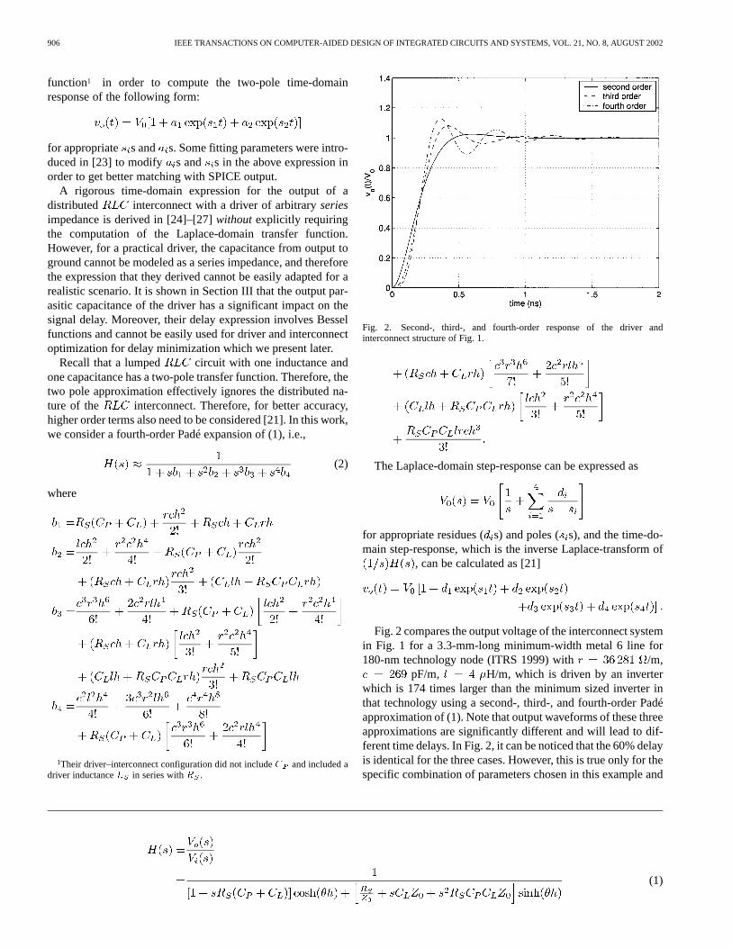
Fig. 2. Second-, third-, and fourth-order response of the driver andinterconnect structure of Fig. 1.
The Laplace-domain step-response can be expressed as
for appropriate residues (s) and poles ( s), and the time-do-main step-response, which is the inverse Laplace-transform of
, can be calculated as [21]
Fig. 2 compares the output voltage of the interconnect systemin Fig. 1 for a 3.3-mm-long minimum-width metal 6 line for180-nm technology node (ITRS 1999) with /m,
pF/m, H/m, which is driven by an inverterwhich is 174 times larger than the minimum sized inverter inthat technology using a second-, third-, and fourth-order Padéapproximation of (1). Note that output waveforms of these threeapproximations are significantly different and will lead to dif-ferent time delays. In Fig. 2, it can be noticed that the 60% delayis identical for the three cases. However, this is true only for thespecific combination of parameters chosen in this example and
(1)

BANERJEE AND MEHROTRA: ANALYSIS OF ON-CHIP INDUCTANCE EFFECTS FOR DISTRIBUTED INTERCONNECTS 907
Fig. 3. Step response of the driver and interconnect structure for three cases:1)R andC the same as in Fig. 2; 2)C = 0; and 3)C = 0 andR = 0.Other parameters are same as those for Fig. 2.
is not true for any other combination or for other delay frac-tions. It should be noted that the delay is not a smooth functionof for a fourth-order response. Therefore, if a fourth-order re-sponse is used for delay computation and optimization, the re-sulting optimum interconnect lengths and driver sizes may alsonot be smooth functions of. However, the magnitude of the re-sultingkink is very small as will be illustrated later.
III. EFFECT OFDRIVER CHARACTERISTICS ONTIME-DOMAIN
RESPONSE
Driver resistance and output capacitance have a sig-nificant effect on the waveform and delay. Previous analyseshave either considered ideal drivers, i.e., ignored bothand
[23] or ignored [22], [24]–[27]. Ignoring leads tolarge errors in delay expressions and interconnect length opti-mization for delay minimization cannot be performed if. Ignoring also introduces nonnegligible errors in delay
computation if is comparable to and line capacitance.For DSM technologies, the parasitic output capacitance is ac-tually larger than and therefore must also be accounted for.Fig. 3 shows that the step response as well as the delay for dis-tributed lines are significantly affected if or areignored [21].
IV. PERFORMANCEOPTIMIZATION METHODOLOGY
Ismail and Friedman [28], [29] presented empirical formulasfor finding the optimum buffer size and interconnect length tominimize the delay in an interconnect of a fixed length. Anempirical expression for the 50% delay, which was obtainedby curve-fitting circuit simulation results, was minimized, andoptimized values of repeater size and interbuffer interconnectlength were plotted. Using these plots, empirical formulas foroptimized values of repeater size and interconnect length wereobtained using curve fitting. However, the delay formula is ap-plicable only if the ratio of total line capacitance to load capac-itance and the ratio of source resistance to total line
Fig. 4. Long interconnect broken up into buffered segments.
resistance is between 0 and 1. Furthermore, is notconsidered in their formulation which seriously compromisesthe validity of the curve-fitted parameters.
We now present a new approach [20] of optimizing repeatersizes and interconnect lengths which does not suffer from thelimitations of the approach of [28], [29]. In our approach thedelay (3) is directly solved using numerical techniques for anyvalues of without any curve fitting with circuit simulation re-sults.
For a step input, the (where ) delay, ,(i.e., ) is the solution to the following:
(3)
For given values of s and s, the above equation can be solvednumerically (for instance, using Newton–Raphson method) tocompute the value of.
Consider a long interconnect of length. In order to mini-mize its delay, the line is broken up into buffered segments oflength , each of which is driven by a buffer of sizeand has adelay (Fig. 4). The overall delay of the line is given by
total delay
Therefore, in order to minimize the total delay, we seek to min-imize thedelay per unit length . Setting the derivative ofdelay per unit length with respect toand to zero we have
(4)
(5)
Differentiating (3) with respect to and and using (4) and (5)we get
(6)
(7)
Equations (6) and (7) can be numerically solved to obtainvalues of buffer size and interconnect lengthwhich minimize the delay per unit length [20]. We used theNewton–Raphson method for this purpose and observed thatconvergence is achieved in less than six iterations in all cases.The computation steps involved in each Newton iteration are asfollows.
1) Find s, s, and s2 and their derivatives w. r. t. and.
2The expressions ofs andd are fairly tedious and are omitted for clarity.

908 IEEE TRANSACTIONS ON COMPUTER-AIDED DESIGN OF INTEGRATED CIRCUITS AND SYSTEMS, VOL. 21, NO. 8, AUGUST 2002
2) Compute by numerically solving (3).3) Compute using (6) and (7) and their derivatives w. r.
t. and .4) Solve
Therefore, this entire optimization step is extremely efficient.Note that the only approximations in the above optimizationsteps are:
1) use of (2) instead of (1) for the transfer function;2) constant and for the entire voltage range.
V. RESULTS AND DISCUSSION
We now apply our optimization technique to the top-levelmetal interconnects for 180-, 130-, 100-, 70-, and 50-nmtechnology nodes as per ITRS specifications [30]. To obtainthe interconnect capacitance per unit lenght, full 3-D capaci-tance extraction of dense wiring networks was performed usingFASTCAP [31]. Here, we summarize our results for the 180-nmtechnology node and point out the salient characteristics of ourperformance optimization solution. The effect of technologyscaling will be addressed in Section VI.
It should be pointed out that a real VLSI interconnect is notan isolated line as shown in Fig. 1 but is embedded in a largemultilevel interconnect system. Therefore, a significant amountof coupling, both capacitive and inductive, can exist between in-terconnects. Typically, interconnects on one layer of metal arerouted in one direction, and on the neighboring metal layers in-terconnects are routed in orthogonal direction. Therefore, thereis minimal capacitive coupling between interconnects on adja-cent metal layers. Additionally, lines on one metal layer coupleonly to their two nearest neighboring lines. The effective line ca-pacitance can therefore change due to Miller effect dependingon the switching activity on these two nearest neighboring lines.Since the aspect ratios of interconnects in DSM technologies istypically greater than one, effective line capacitance can varyby as much as 4. However, as pointed out earlier, since mag-netic fields have much longer spatial range compared to electricfields, line inductance values are sensitive to switching activitieseven in distant lines and therefore experience much larger vari-ation and uncertainty in effective line inductance. In our exper-iments, for simplicity we have assumed that line capacitance isfixed and concentrated on variations in line inductances. Theseresults can be easily modified to incorporate variations in linecapacitance as well.
First consider the case of optimum repeater insertion by con-sidering only the line resistance and capacitance and optimizingthe Elmore delay. The total Elmore delay of interconnect oflength (Fig. 4) is given by
Fig. 5. h =h as a function of line inductance for 180-nmtechnology.
Therefore, the optimum repeater size and interconnectlength is given by
Furthermore, the delay of one segment of length drivenby a buffer of size is given by
Note that is independent of and and, therefore, thewiring level. Thus, it can be treated as a technology parameter.
In general, for a given technology,, , and cannot beeasily determined. Moreover, and are voltage dependent.Therefore, for this study, we find and by SPICEsimulations. These simulations also provide . Using theabove equations, , , and can be then determined for thatparticular technology. Furthermore, for the simulations, we useda ring oscillator, and hence the frequency of the ring oscillatorwas used for the analysis presented in this paper at a given tech-nology node.
We now show the effect of including line inductance in theoptimization as derived in Section IV. It should be noted thatisnot a fixed parameter for a given technology and metal layer butdepends on the current return path and varies substantially withinput vectors. However, a worst case number for line inductancein a dense 3-D interconnect array can be determined as follows:the line inductance would be greatest if the current return pathis through the substrate. Let this inductance be . We havecarried out delay minimization for .
Fig. 5 plots the ratio of the optimum interconnect lengthand the interconnect length optimized for Elmore
delay, . Fig. 6 plots the ratio of the optimum buffer
BANERJEE AND MEHROTRA: ANALYSIS OF ON-CHIP INDUCTANCE EFFECTS FOR DISTRIBUTED INTERCONNECTS 909
Fig. 6. k =k as a function of line inductance for 180-nmtechnology.
Fig. 7. Ratio of optimum delay per unit length,(�=h) , and(�=h) as a function of line inductancel for 180-nm technology.
size and the buffer size optimized for Elmore delay,. These plots also corroborate the observations made
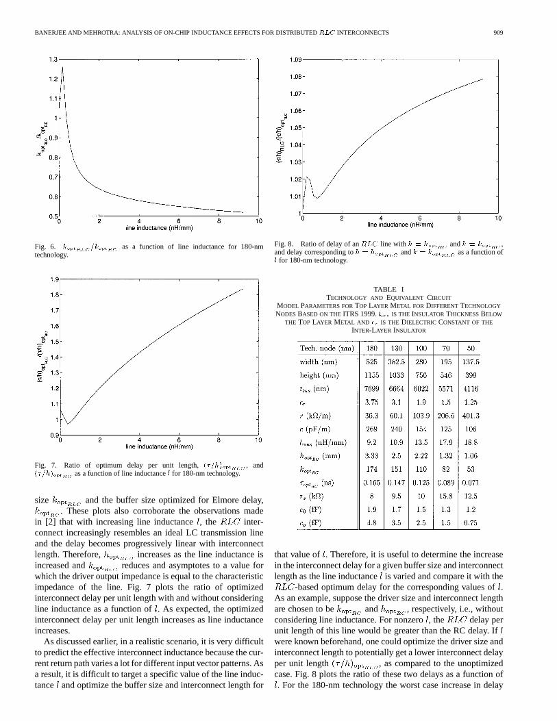
in [2] that with increasing line inductance, the inter-connect increasingly resembles an ideal LC transmission lineand the delay becomes progressively linear with interconnectlength. Therefore, increases as the line inductance isincreased and reduces and asymptotes to a value forwhich the driver output impedance is equal to the characteristicimpedance of the line. Fig. 7 plots the ratio of optimizedinterconnect delay per unit length with and without consideringline inductance as a function of. As expected, the optimizedinterconnect delay per unit length increases as line inductanceincreases.
As discussed earlier, in a realistic scenario, it is very difficultto predict the effective interconnect inductance because the cur-rent return path varies a lot for different input vector patterns. Asa result, it is difficult to target a specific value of the line induc-tance and optimize the buffer size and interconnect length for
Fig. 8. Ratio of delay of anRLC line with h = h andk = k ,and delay corresponding toh = h andk = k as a function ofl for 180-nm technology.
TABLE ITECHNOLOGY AND EQUIVALENT CIRCUIT
MODEL PARAMETERS FORTOP LAYER METAL FOR DIFFERENTTECHNOLOGY
NODESBASED ON THEITRS 1999.t IS THE INSULATOR THICKNESSBELOW
THE TOP LAYER METAL AND � IS THE DIELECTRIC CONSTANT OF THE
INTER-LAYER INSULATOR
that value of . Therefore, it is useful to determine the increasein the interconnect delay for a given buffer size and interconnectlength as the line inductanceis varied and compare it with the
-based optimum delay for the corresponding values of.As an example, suppose the driver size and interconnect lengthare chosen to be and , respectively, i.e., withoutconsidering line inductance. For nonzero, the delay perunit length of this line would be greater than the RC delay. Ifwere known beforehand, one could optimize the driver size andinterconnect length to potentially get a lower interconnect delayper unit length , as compared to the unoptimizedcase. Fig. 8 plots the ratio of these two delays as a function of. For the 180-nm technology the worst case increase in delay
910 IEEE TRANSACTIONS ON COMPUTER-AIDED DESIGN OF INTEGRATED CIRCUITS AND SYSTEMS, VOL. 21, NO. 8, AUGUST 2002
Fig. 9. h =h as a function of line inductancel for varioustechnology nodes.
Fig. 10. k =k as a function of line inductancel for varioustechnology nodes.
over the optimized case is 8%. Therefore, even if the lineinductance were known precisely, in the best case, there wouldbe a meager 8% improvement in the delay per unit length [20].
VI. EFFECT OFTECHNOLOGY SCALING
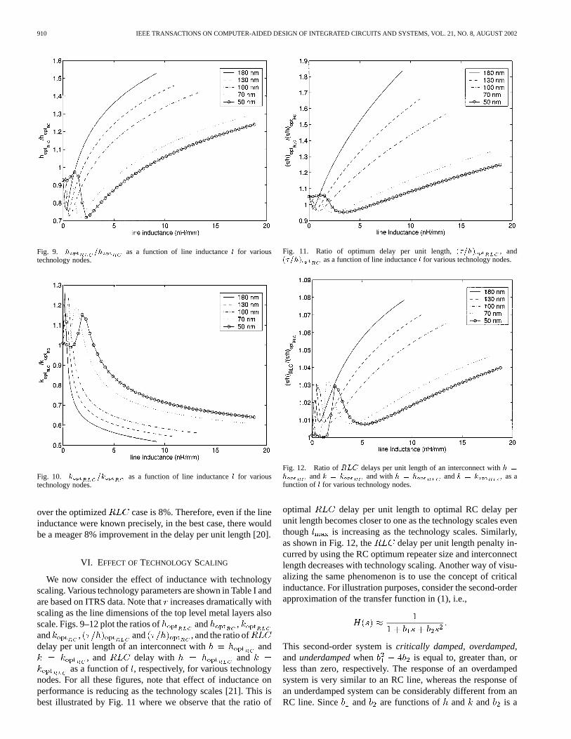
We now consider the effect of inductance with technologyscaling. Various technology parameters are shown in Table I andare based on ITRS data. Note thatincreases dramatically withscaling as the line dimensions of the top level metal layers alsoscale. Figs. 9–12 plot the ratios of and ,and , and , and the ratio ofdelay per unit length of an interconnect with and
, and delay with andas a function of, respectively, for various technology
nodes. For all these figures, note that effect of inductance onperformance is reducing as the technology scales [21]. This isbest illustrated by Fig. 11 where we observe that the ratio of
Fig. 11. Ratio of optimum delay per unit length,(�=h) , and(�=h) as a function of line inductancel for various technology nodes.
Fig. 12. Ratio ofRLC delays per unit length of an interconnect withh =h andk = k and withh = h andk = k as afunction of l for various technology nodes.
optimal delay per unit length to optimal RC delay perunit length becomes closer to one as the technology scales eventhough is increasing as the technology scales. Similarly,as shown in Fig. 12, the delay per unit length penalty in-curred by using the RC optimum repeater size and interconnectlength decreases with technology scaling. Another way of visu-alizing the same phenomenon is to use the concept of criticalinductance. For illustration purposes, consider the second-orderapproximation of the transfer function in (1), i.e.,
This second-order system iscritically damped, overdamped,andunderdampedwhen is equal to, greater than, orless than zero, respectively. The response of an overdampedsystem is very similar to an RC line, whereas the response ofan underdamped system can be considerably different from anRC line. Since and are functions of and and is a

BANERJEE AND MEHROTRA: ANALYSIS OF ON-CHIP INDUCTANCE EFFECTS FOR DISTRIBUTED INTERCONNECTS 911
Fig. 13. Critical inductancel as a function of line inductancel for varioustechnology nodes.
function of , at and , a valuecan be obtained for which
i.e., the system will be critically damped. is given by (8)shown at the bottom of the page, where
Fig. 13 plots this critical inductance as a function of. Recallthat the system is overdamped if . We find that in-creases as the technology scales. From Fig. 13, it can also beobserved that the overdamped criterion is being sat-isfied for a bigger range of line inductances as the technologyscales, which also implies the diminishing effect of line induc-tance with technology scaling [21].
The above analysis has been carried out assuming that thewidth of the topmost metal layer is the minimum width pre-scribed by the ITRS data. However, to reduce signal delay in-terconnects, which are wider than the minimum width, are oftenused in high-performance design. For these lines, the resistanceper unit length is smaller and therefore inductive effects can be-come significant. As an illustration, consider the top layer metalin 100-nm technology node. Five different metal widths are con-sidered: , , , , and . and
are recomputed for each of these widths. Fig. 14 plotsthe delay per unit length as a function ofwhen an inter-connect of length is driven by a buffer of size for
Fig. 14. Delay per unit length for five different line widths for 100-nmtechnology node as a function of line inductance.
each of these line widths. As expected, for very small values of, the delay of the wider lines is much smaller but asincreases,
the advantage of using wider lines diminishes as the differencebetween the delays per unit length for different line widths re-duces.
VII. I NDUCTANCE EFFECTS INUNSCALED GLOBAL LINES
A. Effect of Technology Scaling
Earlier technology scaling predictions, such as NTRS [32],proposed that the metal lines on the topmost metal layer shouldnot be scaled with technology. The main motivation behind thisapproach was to make sure that delay of these global lines doesnot increase and adversely affect performance. However, line in-ductance was not accounted for in these predictions. With tech-nology scaling and increasing clock speeds, the inductive com-ponent of the line impedance becomes the dominant factor ofthe overall line impedance and can adversely affect the perfor-mance with scaling. To investigate this phenomenon further, theexperiments of Section VI were repeated with the dimensions ofglobal lines fixed at values corresponding to the 180-nm tech-nology, i.e., width of 525 nm, height of 1155 nm, distance fromsubstrate of 7.7 m, and dielectric constant of the interlayer di-electric of 3.75. Similar to Fig. 12 in Section VI, Fig. 15 plots theratio of delay per unit length of an line withand and the delay with and
as a function of. In sharp contrast to Fig. 12, thisratio increases with technology scaling indicating the increasingimportance of inductance effects and the need for taking the lineinductance into account for performance optimization. This factis further corroborated in Fig. 16 which plots the critical induc-tance as a function of line inductance for different technologies
(8)

912 IEEE TRANSACTIONS ON COMPUTER-AIDED DESIGN OF INTEGRATED CIRCUITS AND SYSTEMS, VOL. 21, NO. 8, AUGUST 2002
Fig. 15. Ratio of delay corresponding toh = h andk = k anddelay corresponding toh = h andk = k as a function ofl forvarious technology nodes with unscaled global lines.
Fig. 16. Critical inductance as a function of line inductance for varioustechnology nodes with unscaled global lines.
with unscaled global lines. It can be observed that for unscaledglobal lines, the value of decreaseswith scaling, i.e., theline becomes susceptible to inductance effects for a larger rangeof [20].
B. Catastrophic Failures Due to Inductance
The decrease in with technology scaling for unscaledglobal lines implies that the driver–interconnect–load structureis underdamped for a large range of line inductance. As pointedout earlier, the step response of an underdamped system ex-hibits overshoot and undershoot. This overshoot and undershootcan cause catastrophic failures both in terms of device life–timedegradation and errors during the operation of the logic circuits.
1) Logic Failures: As an illustration of this phenomenon,consider a five-stage ring oscillator in the 100-nm technologynode in which each stage consists of an inverter of sizedriving an interconnect of length . Fig. 17 shows the
Fig. 17. Voltage waveform at the input and output of an inverter in a five-stagering oscillator withl = 1:8 nH/mm.
Fig. 18. Voltage waveform at the input and output of an inverter in a five-stagering oscillator withl = 2:2 nH/mm.
voltage waveform at the input and output of an inverter in thisring oscillator obtained from SPICE simulation. The line capac-itance is assumed to be 1.8 nH/mm. Note that even though theinput waveform shows a significant amount of overshoot andundershoot, the inverter output is relatively “clean.” However, ifis increased, the undershoot can become large enough to cause
the inverter to switch and since this inverter is a part of a ringoscillator, the false switching propagates throughout the chainand the period of oscillation becomes very small. Fig. 18 showsthe voltage waveform at the input and output of an inverter inthis ring oscillator with a line inductance of 2.2 nH/mm. Notethat with a small increase in, the period of oscillation is lessthan half of the corresponding period for nH/mm. Toillustrate this phenomenon further, Fig. 19 plots the period ofoscillation as a function line inductance. Around nH/mm,the period drops sharply indicating the onset of false switchingin the circuit. A similar behavior was observed for a five-stagebuffered line which was excited by a square wave at one
BANERJEE AND MEHROTRA: ANALYSIS OF ON-CHIP INDUCTANCE EFFECTS FOR DISTRIBUTED INTERCONNECTS 913
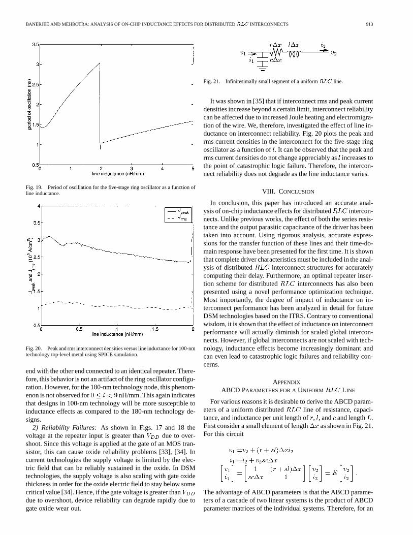
Fig. 19. Period of oscillation for the five-stage ring oscillator as a function ofline inductance.
Fig. 20. Peak and rms interconnect densities versus line inductance for 100-nmtechnology top-level metal using SPICE simulation.
end with the other end connected to an identical repeater. There-fore, this behavior is not an artifact of the ring oscillator configu-ration. However, for the 180-nm technology node, this phenom-enon is not observed for nH/mm. This again indicatesthat designs in 100-nm technology will be more susceptible toinductance effects as compared to the 180-nm technology de-signs.
2) Reliability Failures: As shown in Figs. 17 and 18 thevoltage at the repeater input is greater than due to over-shoot. Since this voltage is applied at the gate of an MOS tran-sistor, this can cause oxide reliability problems [33], [34]. Incurrent technologies the supply voltage is limited by the elec-tric field that can be reliably sustained in the oxide. In DSMtechnologies, the supply voltage is also scaling with gate oxidethickness in order for the oxide electric field to stay below somecritical value [34]. Hence, if the gate voltage is greater thandue to overshoot, device reliability can degrade rapidly due togate oxide wear out.
Fig. 21. Infinitesimally small segment of a uniformRLC line.
It was shown in [35] that if interconnect rms and peak currentdensities increase beyond a certain limit, interconnect reliabilitycan be affected due to increased Joule heating and electromigra-tion of the wire. We, therefore, investigated the effect of line in-ductance on interconnect reliability. Fig. 20 plots the peak andrms current densities in the interconnect for the five-stage ringoscillator as a function of. It can be observed that the peak andrms current densities do not change appreciably asincreases tothe point of catastrophic logic failure. Therefore, the intercon-nect reliability does not degrade as the line inductance varies.
VIII. C ONCLUSION
In conclusion, this paper has introduced an accurate anal-ysis of on-chip inductance effects for distributed intercon-nects. Unlike previous works, the effect of both the series resis-tance and the output parasitic capacitance of the driver has beentaken into account. Using rigorous analysis, accurate expres-sions for the transfer function of these lines and their time-do-main response have been presented for the first time. It is shownthat complete driver characteristics must be included in the anal-ysis of distributed interconnect structures for accuratelycomputing their delay. Furthermore, an optimal repeater inser-tion scheme for distributed interconnects has also beenpresented using a novel performance optimization technique.Most importantly, the degree of impact of inductance on in-terconnect performance has been analyzed in detail for futureDSM technologies based on the ITRS. Contrary to conventionalwisdom, it is shown that the effect of inductance on interconnectperformance will actually diminish for scaled global intercon-nects. However, if global interconnects are not scaled with tech-nology, inductance effects become increasingly dominant andcan even lead to catastrophic logic failures and reliability con-cerns.
APPENDIX
ABCD PARAMETERS FOR AUNIFORM LINE
For various reasons it is desirable to derive the ABCD param-eters of a uniform distributed line of resistance, capaci-tance, and inductance per unit length of, , and and length .First consider a small element of length as shown in Fig. 21.For this circuit
The advantage of ABCD parameters is that the ABCD parame-ters of a cascade of two linear systems is the product of ABCDparameter matrices of the individual systems. Therefore, for an
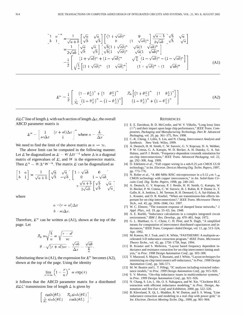
914 IEEE TRANSACTIONS ON COMPUTER-AIDED DESIGN OF INTEGRATED CIRCUITS AND SYSTEMS, VOL. 21, NO. 8, AUGUST 2002
(A1)
(A2)
line of length with each section of length , the overallABCD parameter matrix is
where
We need to find the limit of the above matrix as .The above limit can be computed in the following manner.
Let be diagonalized as where is a diagonalmatrix of eigenvalues of , and is the eigenvector matrix.Then . The matrix can be diagonalized as
where
Therefore, can be written as (A1), shown at the top of thepage. Let
Substituting these in (A1), the expression for becomes (A2),shown at the top of the page. Using the identity
it follows that the ABCD parameter matrix for a distributedtransmission line of length is given by
REFERENCES
[1] E. E. Davidson, B. D. McCredie, and W. V. Vilkelis, “Long lossy lines(L ) and their impact upon large chip performance,”IEEE Trans. Com-ponents, Packaging and Manufacturing Technology, Part B: AdvancedPackaging, vol. 20, pp. 361–375, Nov. 1998.
[2] C.-K. Cheng, J. Lillis, S. Lin, and N. Chang,Interconnect Analysis andSynthesis. New York: Wiley, 1999.
[3] A. Deutsch, H. H. Smith, C. W. Surovic, G. V. Kopcsay, D. A. Webber,P. W. Coteus, G. A. Katopis, W. D. Becker, A. H. Dansky, G. A. Sai-Halasz, and P. J. Restle, “Frequency-dependent crosstalk simulation foron-chip interconnections,”IEEE Trans. Advanced Packaging, vol. 22,pp. 292–308, Aug. 1999.
[4] D. Edelsteinet al., “Full copper wiring in a sub-0.25�m CMOS ULSItechnology,” inInt. Electron. Devices Meeting Dig. Techn. Papers, 1997,pp. 773–776.
[5] N. Roheret al., “A 480 MHz RISC microprocessor in a 0.12�m LCMOS technology with copper interconnects,” inInt. Solid-State Cir-cuits Conf. Dig. Techn. Papers, 1998, pp. 240–241.
[6] A. Deutsch, G. V. Kopcsay, P. J. Restle, H. H. Smith, G. Katopis, W.D. Becker, P. W. Coteus, C. W. Surovic, B. J. Rubin, R. P. Dunne Jr., T.Gallo, K. A. Jenkins, L. M. Terman, R. H. Dennard, G. A. Sai-Halasz, B.L. Krauter, and D. R. Knebel, “When are transmission-line effects im-portant for on-chip interconnections?,”IEEE Trans. Microwave TheoryTech., vol. 45, pp. 1836–1846, Oct. 1997.
[7] W. C. Elmore, “The transient response of damped linear networks,”J.Appl. Phys., vol. 19, pp. 55–63, Jan. 1948.
[8] A. E. Ruehli, “Inductance calculations in a complex integrated circuitenvironment,”IBM J. Res. Develop., pp. 470–481, Sept. 1972.
[9] G. L. Matthaei, G. C. Chinn, C. H. Plott, and N. Dagli, “A simplifiedmeans for computation of interconnect distributed capacitances and in-ductances,”IEEE Trans. Computer-Aided Design, vol. 11, pp. 513–524,Apr. 1992.
[10] M. Kamon, M. J. Tsuk, and J. K. White, “FASTHENRY: A multipole-ac-celerated 3-D inductance extraction program,”IEEE Trans. MicrowaveTheory Techn., vol. 42, pp. 1750–1758, Sept. 1994.
[11] B. Krauter and S. Mehrotra, “Layout based frequency dependent in-ductance and resistance extraction for on-chip interconnect timing anal-ysis,” in Proc. 1998 Design Automation Conf., pp. 303–308.
[12] Y. Massoud, S. Majors, T. Bustami, and J. White, “Layout techniques forminimizing on-chip interconnect self-inductance,” inProc. 1998 DesignAutomation Conf., pp. 566–571.
[13] M. W. Beattie and L. T. Pillegi, “IC analyzes including extracted induc-tance models,” inProc. 1999 Design Automation Conf., pp. 915–920.
[14] S. V. Morton, “On-chip inductance issues in multiconductor systems,”in Proc. 1999 Design Automation Conf., pp. 921–926.
[15] N. Chang, S. Lin, L. He, O. S. Nakagawa, and W. Xie, “Clocktree RLCextraction with efficient inductance modeling,” inProc. Design, Au-tomation and Test Eur. Conf. and Exhibition, 2000, pp. 522–526.
[16] B. Kleveland, X. Qi, L. Madden, R. W. Dutton, and S. S. Wong, “Lineinductance extraction and modeling in a real chip with power grid,” inInt. Electron. Devices Meeting Techn. Dig., 1999, pp. 901–904.
BANERJEE AND MEHROTRA: ANALYSIS OF ON-CHIP INDUCTANCE EFFECTS FOR DISTRIBUTED INTERCONNECTS 915
[17] X. Qi, B. Kleveland, Z. Yu, S. S. Wong, R. W. Dutton, and T. Young,“On-chip inductance modeling of VLSI interconnects,” in2000 IEEEInt. Solid-State Circuits Conf. Dig. Techn. Papers, 2000, pp. 172–173.
[18] K. Gala, V. Zolotov, R. Panda, B. Young, J. Wang, and D. Blaauw,“On-chip inductance modeling and analysis,” inProc. Design Automa-tion Conf., 2000, pp. 63–68.
[19] S. Lin, N. Chang, and S. Nakagawa, “Quick on-chip self- and mutual-in-ductance screen,” inProc. IEEE First Int. Symp. Quality Electron. De-sign, 2000, pp. 513–520.
[20] K. Banerjee and A. Mehrotra, “Analysis of on-chip inductance effectsusing a novel performance optimization methodology for distributedRLC interconnects,” inProc. 2001 Design Automation Conf., pp.798–803.
[21] , “Accurate analysis of on-chip inductance effects and implicationsfor optimal repeater insertion and technology scaling,” inProc. 2001IEEE Symp. VLSI Circuits, pp. 195–198.
[22] A. B. Kahng and S. Muddu, “An analytical delay model for RLCinterconnects,”IEEE Trans. Computer-Aided Design, vol. 16, pp.1507–1514, Dec. 1997.
[23] Y. Cao, X. Huang, D. Sylvester, N. Chang, and C. Hu, “A new analyticaldelay and noise model for on-chip RLC interconnect,” inTechn. Dig.IEDM 2000, pp. 731–734.
[24] J. A. Davis and J. D. Meindl, “Compact distributed RLC models formultilevel interconnect networks,” in1999 Symp. VLSI Technol. Dig.Techn. Papers, 1999, pp. 165–166.
[25] , “Compact distributed RLC models for multilevel interconnectnetworks,” in1999 Symp. VLSI Circuits Dig. Techn. Papers, 1999, pp.167–168.
[26] , “Compact distributed RLC interconnect models-Part I. single linetransient, time delay, and overshoot expressions,”IEEE Trans. Electron.Devices, vol. 47, pp. 2068–2077, Nov. 2000.
[27] , “Compact distributed RLC interconnect models-Part II. Coupledline transient expressions and peak crosstalk in multilevel networks,”IEEE Trans. Electron. Devices, vol. 47, pp. 2078–2087, Nov. 2000.
[28] Y. I. Ismail and E. G. Friedman, “Effects of inductance on the propa-gation delay and repeater insertion in VLSI circuits,” inProc. DesignAutomation Conf., 1999, pp. 721–724.
[29] , “Effects of inductance on the propagation delay and repeater in-sertion in VLSI circuits,”IEEE Trans. VLSI Syst., vol. 8, pp. 195–206,Apr. 2000.
[30] Int. Technol. Roadmap for Semiconductors (ITRS), 1999.[31] K. Nabors and J. K. White, “FASTCAP: A multipole-accelerated 3-D
capacitance extraction program,”IEEE Trans. Computer-Aided Design,vol. 10, pp. 1447–1459, Nov. 1991.
[32] Nat. Technol. Roadmap for Semiconductors (NTRS), 1997.[33] C. Hu, “MOSFET scaling in the next decade and beyond,”Semicon-
ductor Int., pp. 105–114, 1994.[34] , “Gate oxide scaling limits and projection,” inInt. Electron. De-
vices Meeting Dig. Techn. Papers, 1997, pp. 319–322.[35] K. Banerjee, A. Mehrotra, A. Sangiovanni-Vincentelli, and C. Hu, “On
thermal effects in deep sub-micron VLSI interconnects,” inProc. DesignAutomation Conf., 1999, pp. 885–891.
Kaustav Banerjee(S’94–M’99) received the Ph.D.degree in electrical engineering and computersciences from the University of California, Berkeley,in 1999.
He was with Stanford University, Stanford, CA,from 1999 to 2002, as a Research Associate at theCenter for Integrated Systems. In July 2002, hejoined the faculty of the University of California,Santa Barbara, as an Assistant Professor with theDepartment of Electrical and Computer Engineering.His research interests include nanometer scale circuit
effects and their implications for high-performance/low-power VLSI andmixed-signal designs and their design automation methods. He is also inter-ested in some exploratory interconnect and circuit architectures such as 3-DICs, integrated optoelectronics, and nanotechnologies such as single electrontransistors. He co-mentors several doctoral students at Stanford University. Healso co-advises doctoral students in the Electrical Engineering Departmentsof the University of Southern California, Los Angeles, and the Swiss FederalInstitute of Technology (EPFL), Lausanne, Switzerland. From February 2002to August 2002, he was a Visiting Professor at the Microprocessor ResearchLabs of Intel, Hillsboro, OR. In the past, he has also held summer/visitingpositions at Texas Instruments Inc., Dallas, TX, and EPFL-Switzerland, andserved as consultant for Magma Design Automation, Cupertino, CA, andFujitsu Labs of America, Sunnyvale, CA. He has authored or coauthored over70 technical papers in archival journals and refereed international conferencesand has presented numerous invited talks and tutorials.
Dr. Banerjee served as Technical Program Chair of the 2002 IEEE Interna-tional Symposium on Quality Electronic Design (ISQED ’02) and is the Confer-ence Vice-Chair of ISQED ’03. He also serves on the technical program commit-tees of the ACM International Symposium on Physical Design, the EOS/ESDSymposium, and the IEEE International Reliability Physics Symposium. He isthe recipient of a Best Paper Award at the 2001 ACM Design Automation Con-ference.
Amit Mehrotra (S’96–M’99) received the B.Tech.degree in electrical engineering from the Indian Insti-tute of Technology, Kanpur, in 1994 and the M.S. andPh.D. degrees from the Department of Electical En-gineering and Computer Science, University of Cal-ifornia, Berkeley, in 1996 and 1999, respectively.
In August 1999, he joined the University ofIllinois, Urbana-Champaign, where he is currentlyan Assistant Professor with the Department ofElectical and Computer Engineering and a ResearchAssistant Professor with the Illinois Center for
Integrated Micro-Systems group at the Coordinated Science Laboratory. Hisresearch interests include analysis techniques for RF circuits, design techniquesfor low-power mobile communication systems, interconnect performanceanalysis of VLSI systems, and numerical analysis of electrical and mixedelectrical–mechanical systems.