
Analog Signal Conditioning
115
Chapter 2 Analog Signal Conditioning
-
Upload
ammad-ilyas -
Category
Documents
-
view
171 -
download
17
description
Analog Signal Conditioning
Transcript of Analog Signal Conditioning
Chapter 2
Analog Signal Conditioning
Signal Conditioning
• Signal conditioning is the operation
performed on the signal to convert them to
a form suitable for interfacing with other
elements in the process control.elements in the process control.
Signal Conditioning
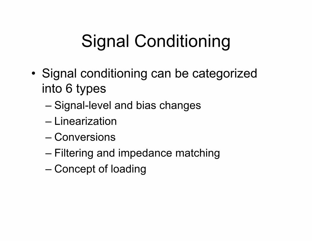
• Signal conditioning can be categorized
into 6 types
– Signal-level and bias changes
– Linearization– Linearization
– Conversions
– Filtering and impedance matching
– Concept of loading
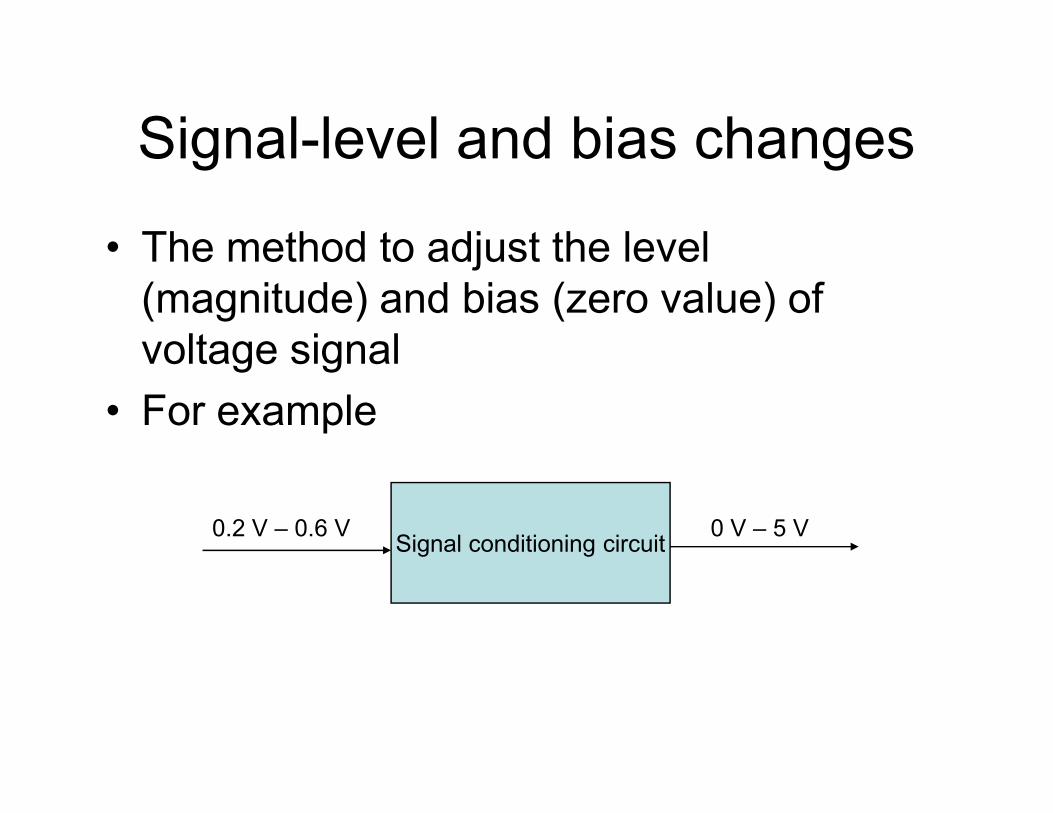
Signal-level and bias changes
• The method to adjust the level
(magnitude) and bias (zero value) of
voltage signal
• For example• For example
Signal conditioning circuit0.2 V – 0.6 V 0 V – 5 V
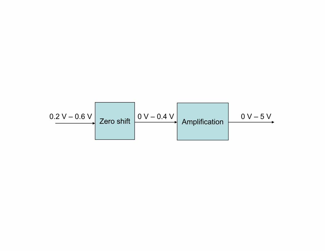
Zero shift0.2 V – 0.6 V 0 V – 5 V
Amplification0 V – 0.4 V
Amplification
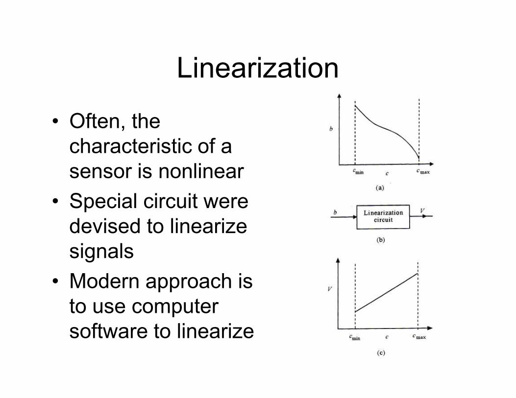
Linearization
• Often, the
characteristic of a
sensor is nonlinear
• Special circuit were • Special circuit were
devised to linearize
signals
• Modern approach is
to use computer
software to linearize
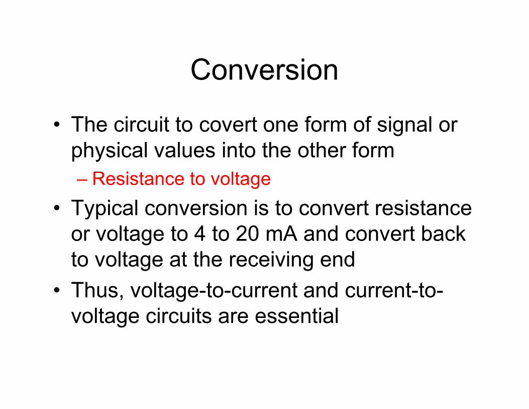
Conversion
• The circuit to covert one form of signal or
physical values into the other form
– Resistance to voltage
• Typical conversion is to convert resistance • Typical conversion is to convert resistance
or voltage to 4 to 20 mA and convert back
to voltage at the receiving end
• Thus, voltage-to-current and current-to-
voltage circuits are essential
Digital Interface
• The use of computer is process control
requires the conversion of analog to digital
signal
– ADC– ADC
– DAC
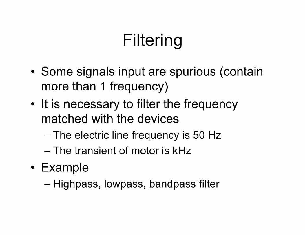
Filtering
• Some signals input are spurious (contain
more than 1 frequency)
• It is necessary to filter the frequency
matched with the devicesmatched with the devices
– The electric line frequency is 50 Hz
– The transient of motor is kHz
• Example
– Highpass, lowpass, bandpass filter
Impedance Matching
• Connecting the sensors or process control
element with different impedance causes
signal reflection
• The network or circuit to match impedance • The network or circuit to match impedance
thus to reduce signal reflection
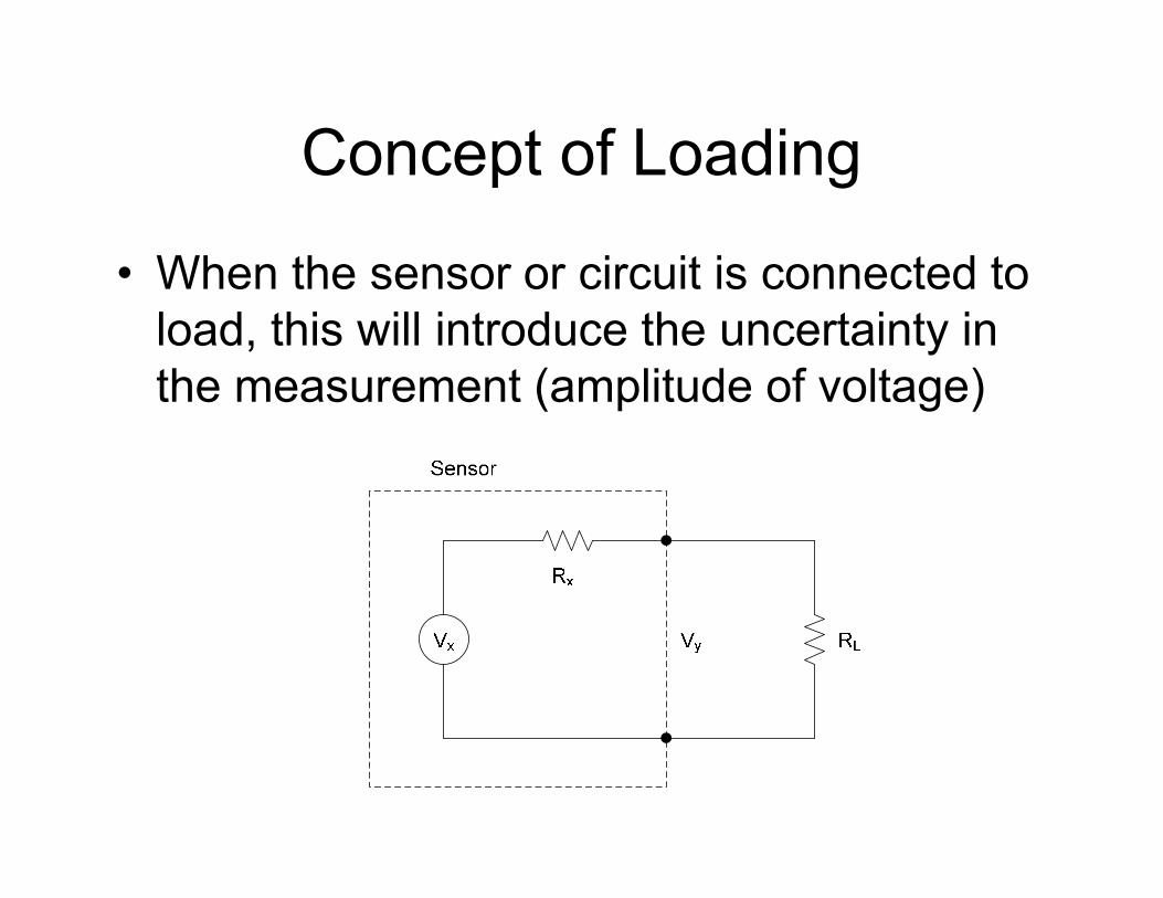
Concept of Loading
• When the sensor or circuit is connected to
load, this will introduce the uncertainty in
the measurement (amplitude of voltage)
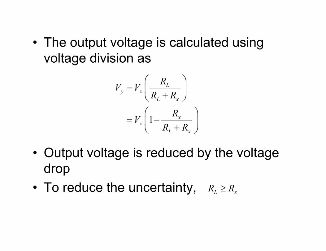
• The output voltage is calculated using
voltage division as
1
Ly x
L x
xx
RV V
R R
RV
R R
=
+
= −
+
• Output voltage is reduced by the voltage
drop
• To reduce the uncertainty,
x
L xR R
+
L xR R≥
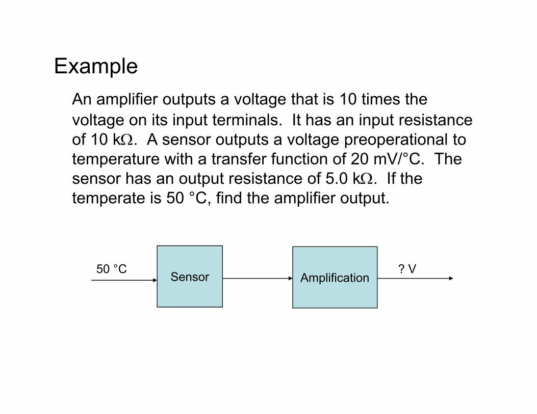
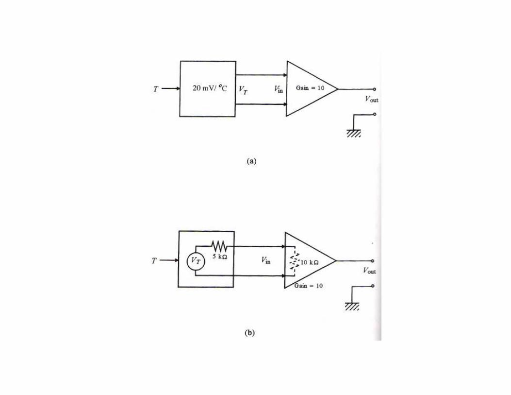
Example
An amplifier outputs a voltage that is 10 times the
voltage on its input terminals. It has an input resistance
of 10 kΩ. A sensor outputs a voltage preoperational to
temperature with a transfer function of 20 mV/°C. The
sensor has an output resistance of 5.0 kΩ. If the
temperate is 50 °C, find the amplifier output.
Sensor50 °C ? V
Amplification
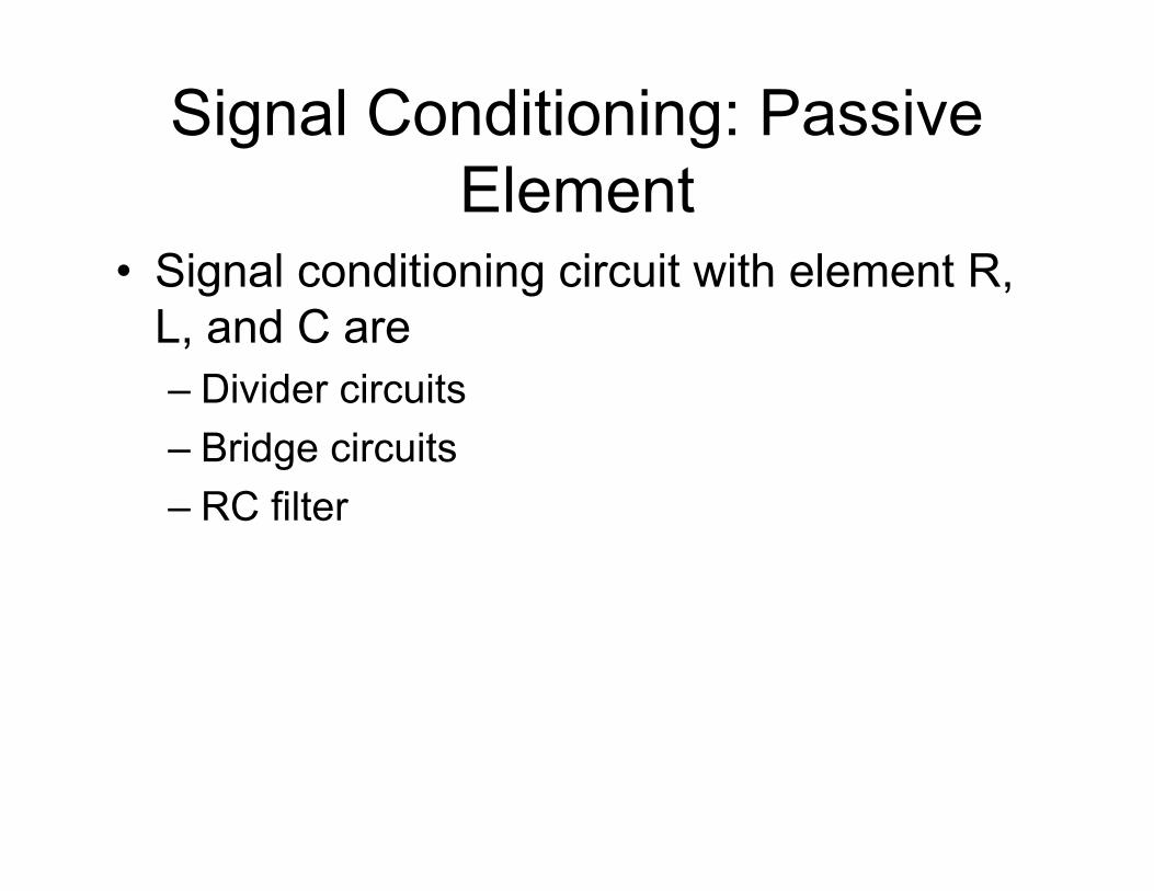
Signal Conditioning: Passive
Element• Signal conditioning circuit with element R,
L, and C are
– Divider circuits
– Bridge circuits– Bridge circuits
– RC filter
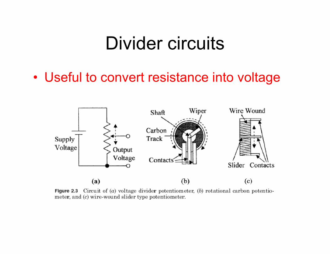
Divider circuits
• Useful to convert resistance into voltage
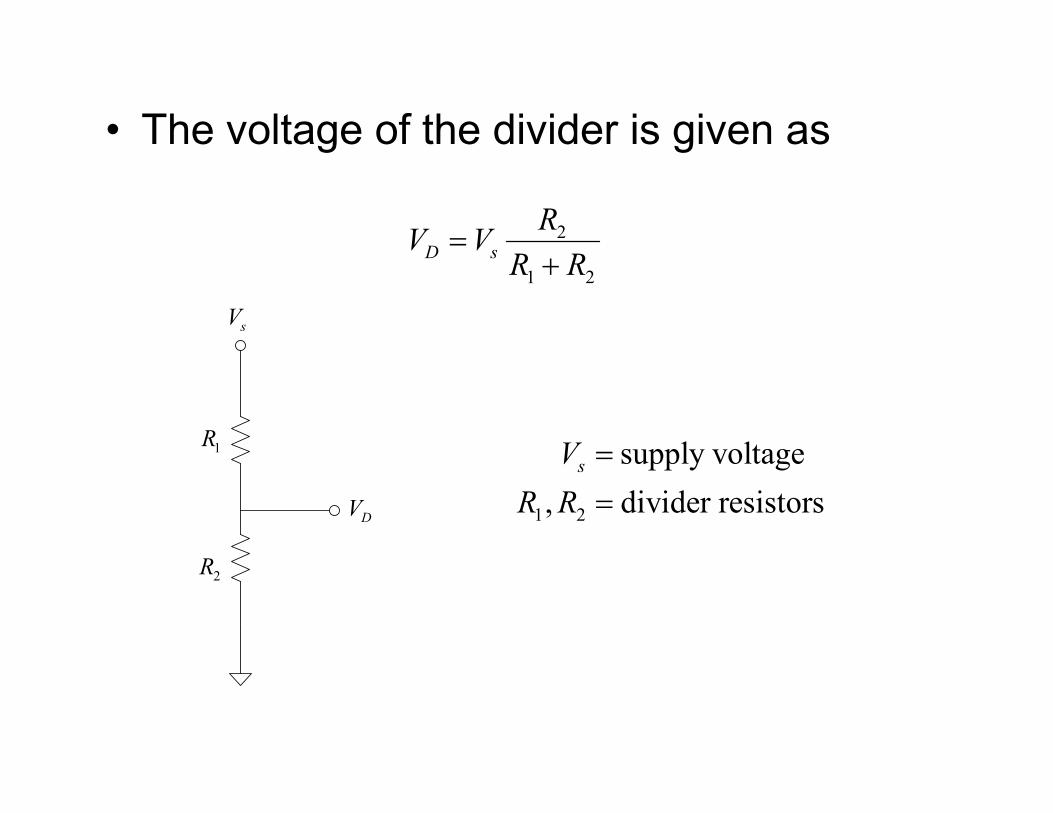
• The voltage of the divider is given as
2
1 2
D s
RV V
R R=
+
sV
DV
1R
2R
1 2
supply voltage
, divider resistors
sV
R R
=
=
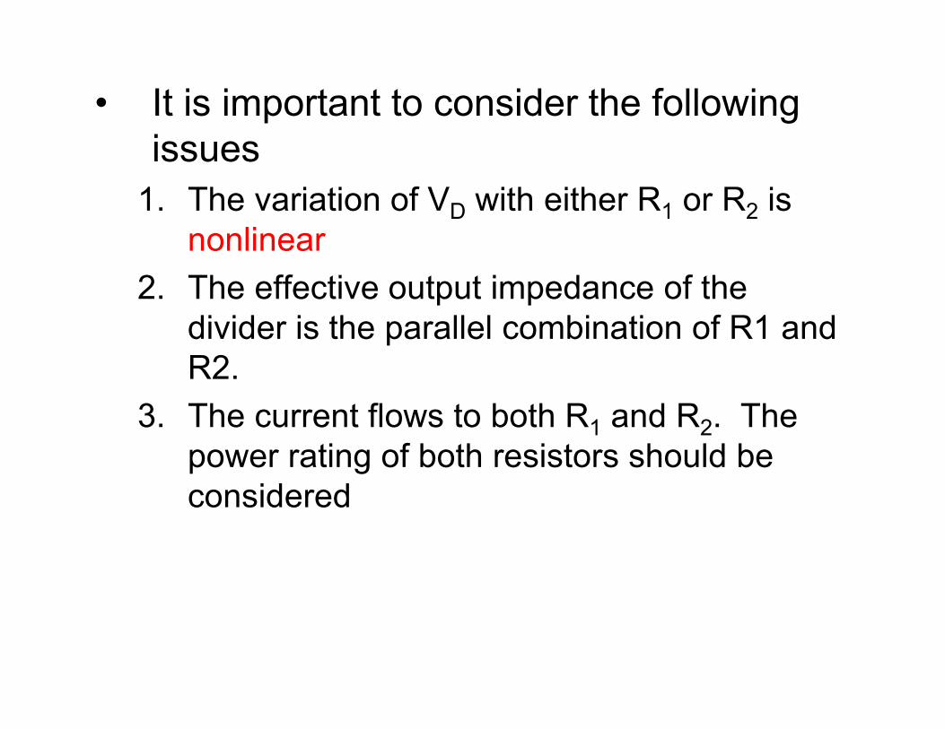
• It is important to consider the following
issues
1. The variation of VD with either R1 or R2 is
nonlinear
2. The effective output impedance of the
divider is the parallel combination of R1 and
R2.R2.
3. The current flows to both R1 and R2. The
power rating of both resistors should be
considered
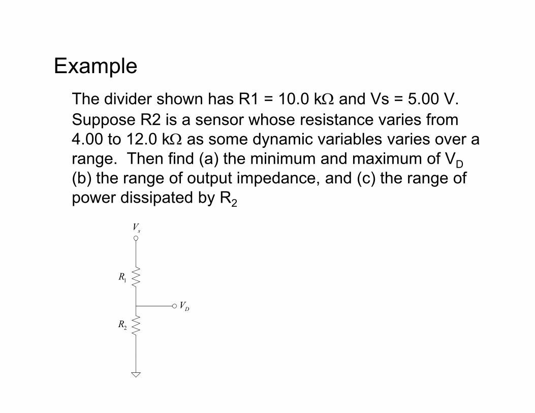
Example
The divider shown has R1 = 10.0 kΩ and Vs = 5.00 V.
Suppose R2 is a sensor whose resistance varies from
4.00 to 12.0 kΩ as some dynamic variables varies over a
range. Then find (a) the minimum and maximum of VD
(b) the range of output impedance, and (c) the range of
power dissipated by R2
sV
DV
1R
2R
Bridge Circuit
• Bridge circuits are used to convert
impedance variations into voltage
variations.
• Application of bridge circuits is in precise • Application of bridge circuits is in precise
static measurement of an impedance
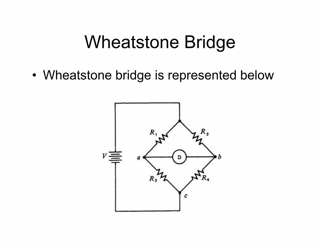
Wheatstone Bridge
• Wheatstone bridge is represented below
• The potential difference ∆V between
points A and B is simply
Where
A BV V V∆ = −
3RV V= 3
1 3
AV VR R
=+
4
2 4
B
RV V
R R=
+
Bridge supply voltageV =
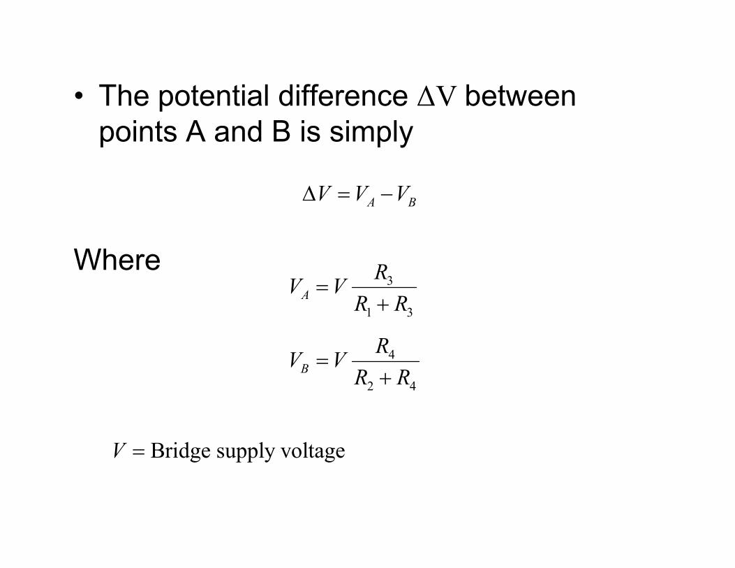
• The voltage difference between A and B is
• The equation above can be reduced to
3 4
1 3 2 4
VR VRV
R R R R∆ = −
+ +
• At particular combination of resistance
values, the voltage difference is zero
( )( )3 2 1 4
1 3 2 4
R R R RV V
R R R R
−∆ =
+ +
3 2 1 4R R R R=
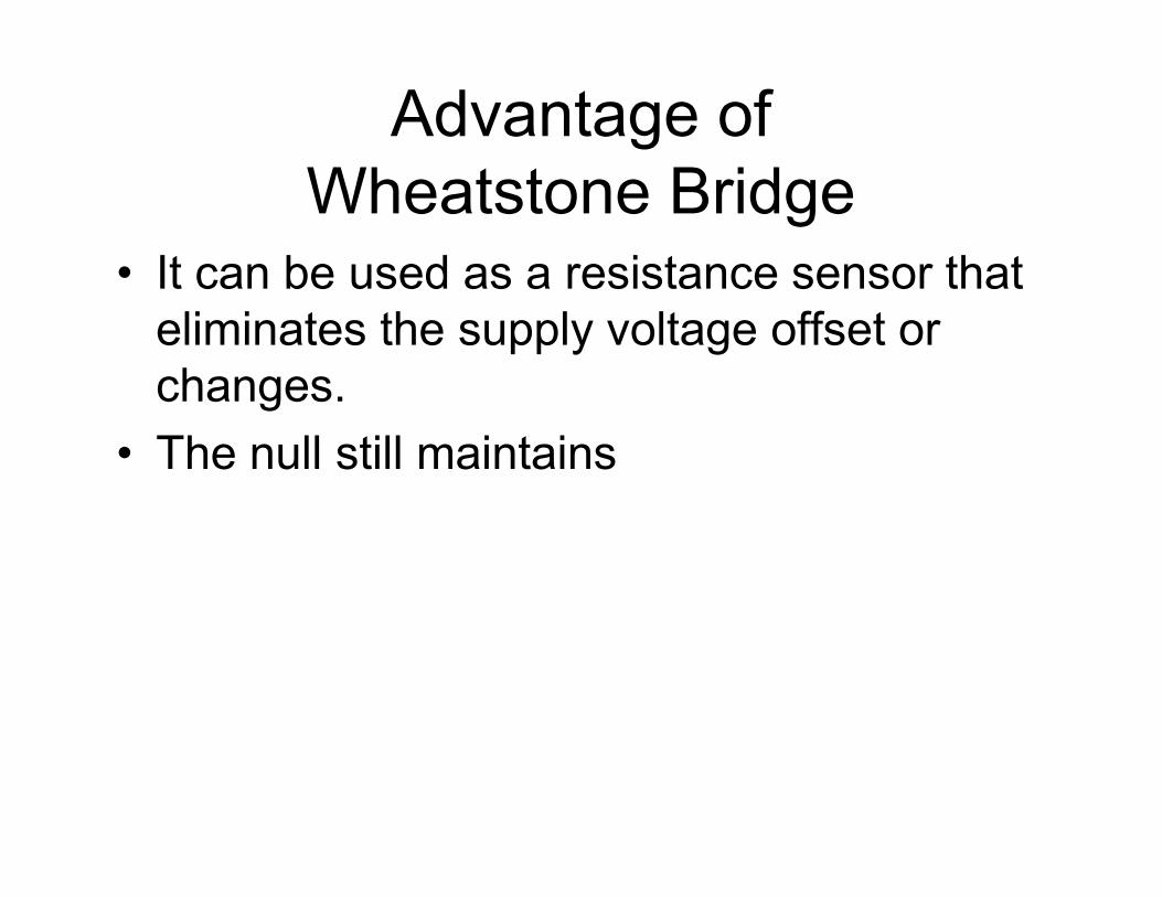
Advantage of
Wheatstone Bridge• It can be used as a resistance sensor that
eliminates the supply voltage offset or
changes.
• The null still maintains• The null still maintains
Galvanometer detector
• Galvanometer is used as a null detector in
the Wheatstone bridge to detect the
condition of the Wheatstone bridge
• And it is required to determine the current • And it is required to determine the current
offset instead of voltage offset
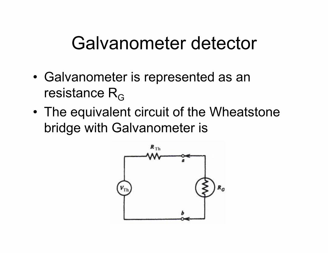
Galvanometer detector
• Galvanometer is represented as an
resistance RG
• The equivalent circuit of the Wheatstone
bridge with Galvanometer is bridge with Galvanometer is
Galvanometer detector
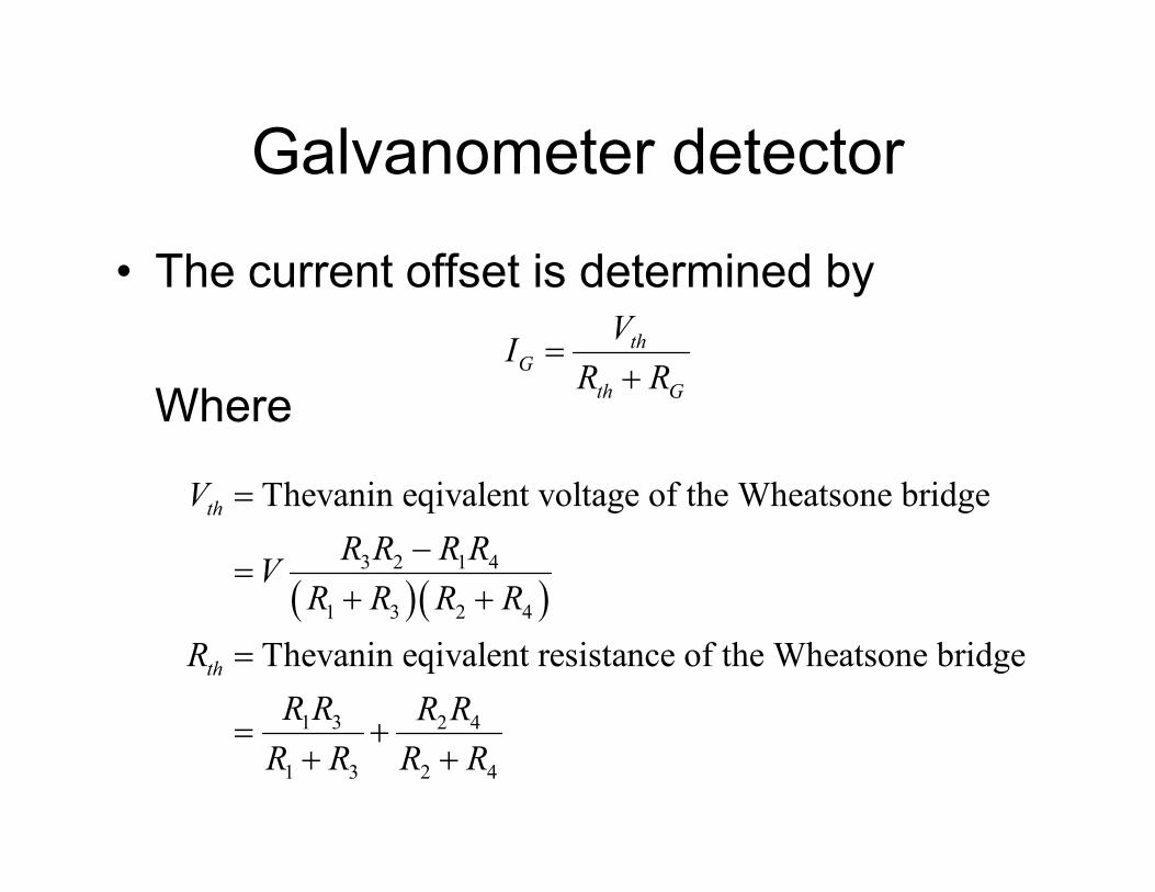
• The current offset is determined by
Where
thG
th G
VI
R R=
+
( )( )3 2 1 4
1 3 2 4
1 3 2 4
1 3 2 4
Thevanin eqivalent voltage of the Wheatsone bridge
Thevanin eqivalent resistance of the Wheatsone bridge
th
th
V
R R R RVR R R R
R
R R R R
R R R R
=
−=
+ +
=
= ++ +
Bridge resolution
• The resolution of the bridge is determined
by the resolution of the detector
• We can convert the resolution of the
detector to find the smallest resistance detector to find the smallest resistance
change in the bridge
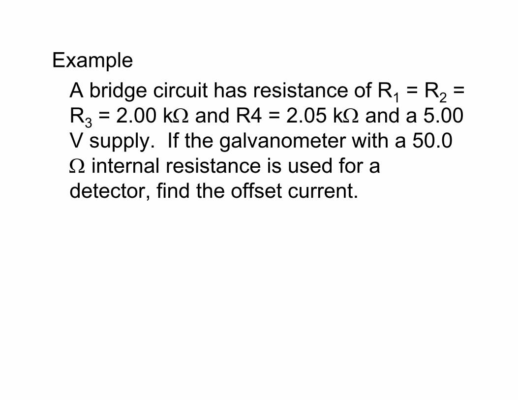
Example
A bridge circuit has resistance of R1 = R2 =
R3 = 2.00 kΩ and R4 = 2.05 kΩ and a 5.00
V supply. If the galvanometer with a 50.0
Ω internal resistance is used for a
detector, find the offset current.detector, find the offset current.
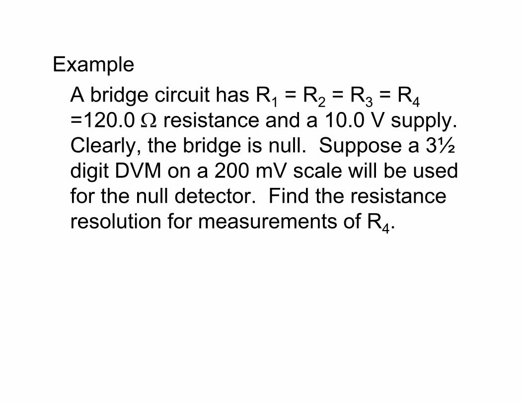
Example
A bridge circuit has R1 = R2 = R3 = R4
=120.0 Ω resistance and a 10.0 V supply.
Clearly, the bridge is null. Suppose a 3½
digit DVM on a 200 mV scale will be used
for the null detector. Find the resistance for the null detector. Find the resistance
resolution for measurements of R4.
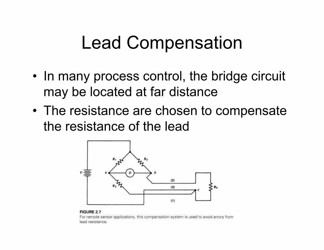
Lead Compensation
• In many process control, the bridge circuit
may be located at far distance
• The resistance are chosen to compensate
the resistance of the leadthe resistance of the lead
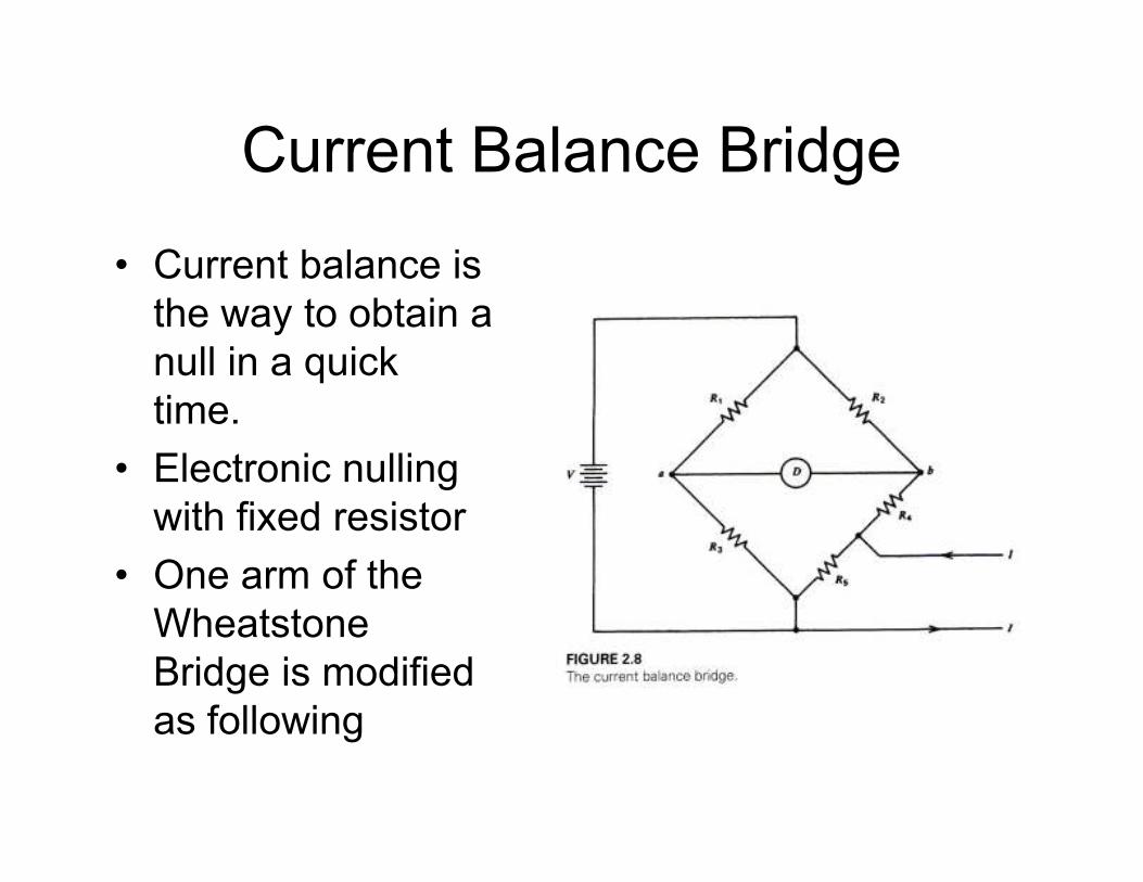
Current Balance Bridge
• Current balance is
the way to obtain a
null in a quick
time.
• Electronic nulling
with fixed resistor
• One arm of the
Wheatstone
Bridge is modified
as following
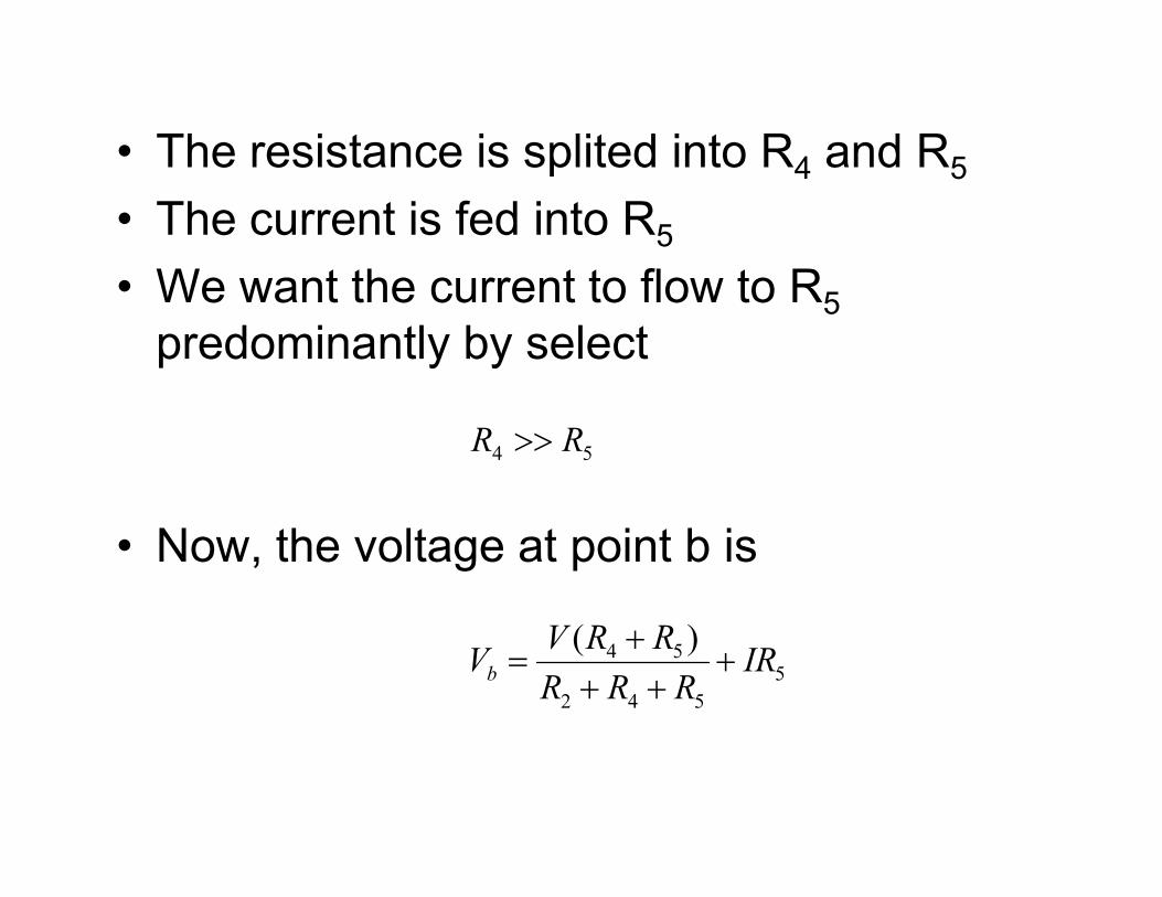
• The resistance is splited into R4 and R5
• The current is fed into R5
• We want the current to flow to R5
predominantly by select
54 RR >>
• Now, the voltage at point b is
4 55
2 4 5
( )b
V R RV IR
R R R
+= +
+ +
54 RR >>
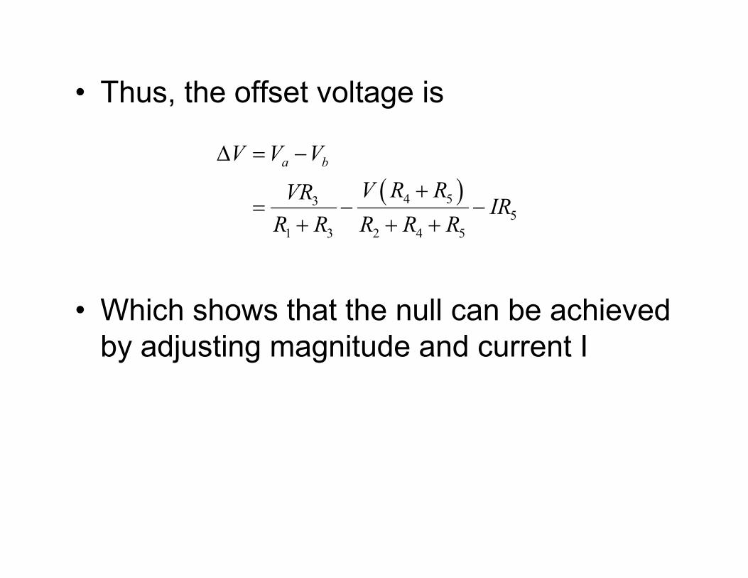
• Thus, the offset voltage is
( )4 535
1 3 2 4 5
a bV V V
V R RVRIR
R R R R R
∆ = −
+= − −
+ + +
• Which shows that the null can be achieved
by adjusting magnitude and current I
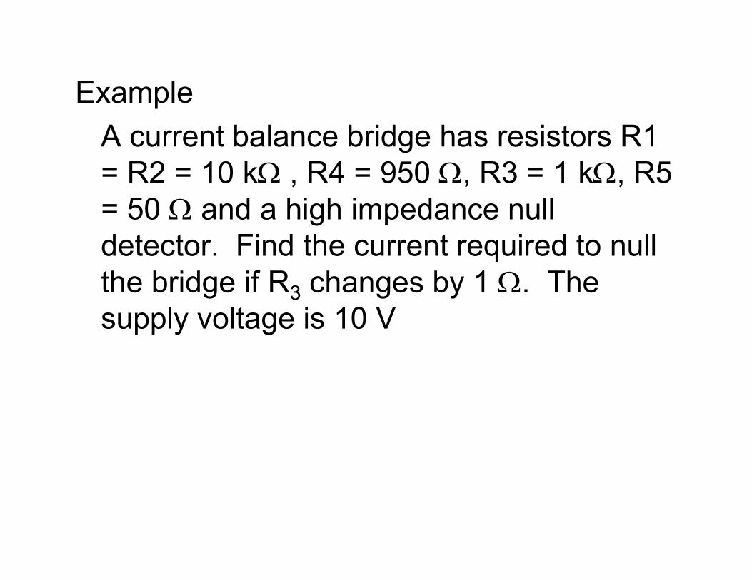
Example
A current balance bridge has resistors R1
= R2 = 10 kΩ , R4 = 950 Ω, R3 = 1 kΩ, R5
= 50 Ω and a high impedance null
detector. Find the current required to null
the bridge if R3 changes by 1 Ω. The the bridge if R3 changes by 1 Ω. The
supply voltage is 10 V
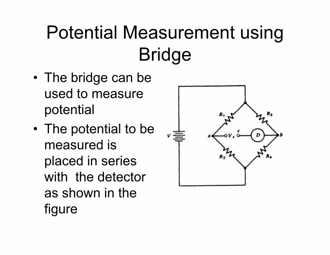
Potential Measurement using
Bridge• The bridge can be
used to measure
potential
• The potential to be • The potential to be
measured is
placed in series
with the detector
as shown in the
figure
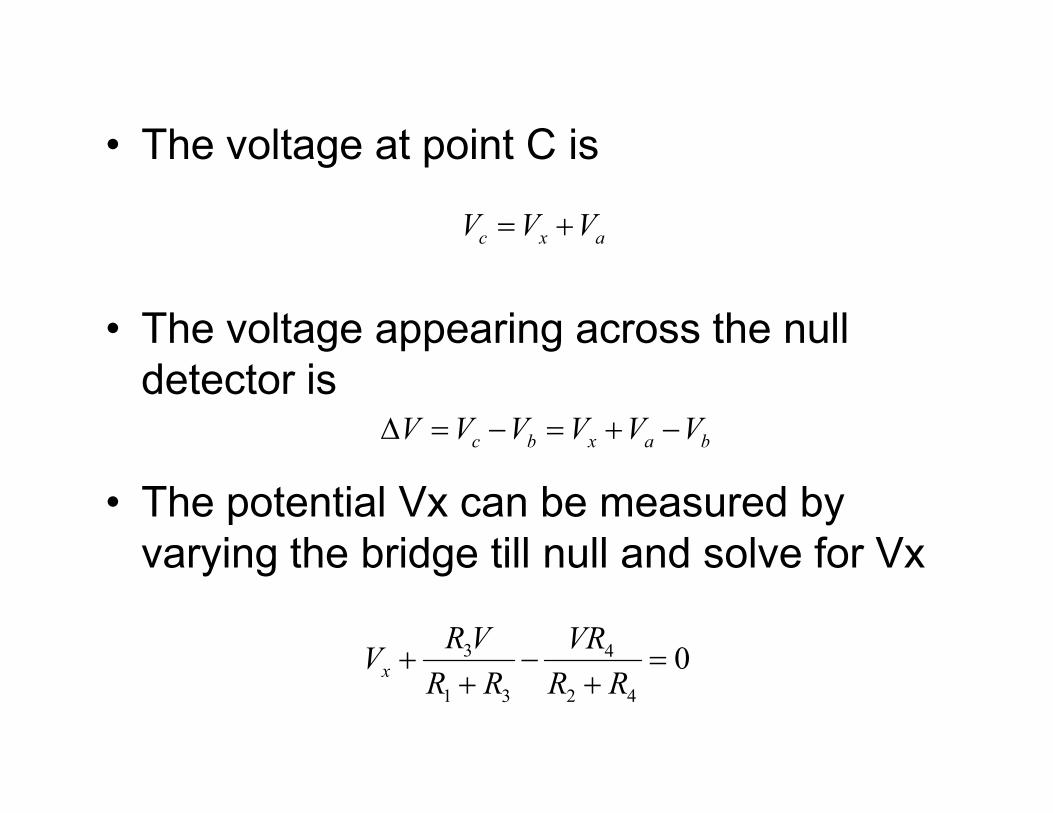
• The voltage at point C is
• The voltage appearing across the null
detector is
c x aV V V= +
• The potential Vx can be measured by
varying the bridge till null and solve for Vx
c b x a bV V V V V V∆ = − = + −
3 4
1 3 2 4
0x
RV VRV
R R R R+ − =
+ +
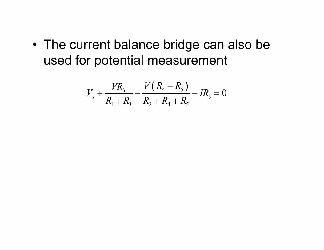
• The current balance bridge can also be
used for potential measurement
( )4 535
1 3 2 4 5
0x
V R RVRV IR
R R R R R
++ − − =
+ + +
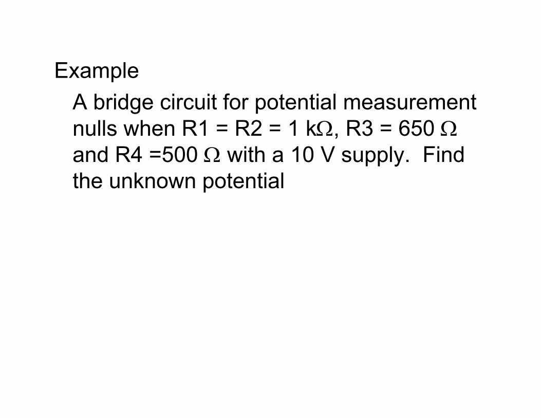
Example
A bridge circuit for potential measurement
nulls when R1 = R2 = 1 kΩ, R3 = 650 Ωand R4 =500 Ω with a 10 V supply. Find
the unknown potential
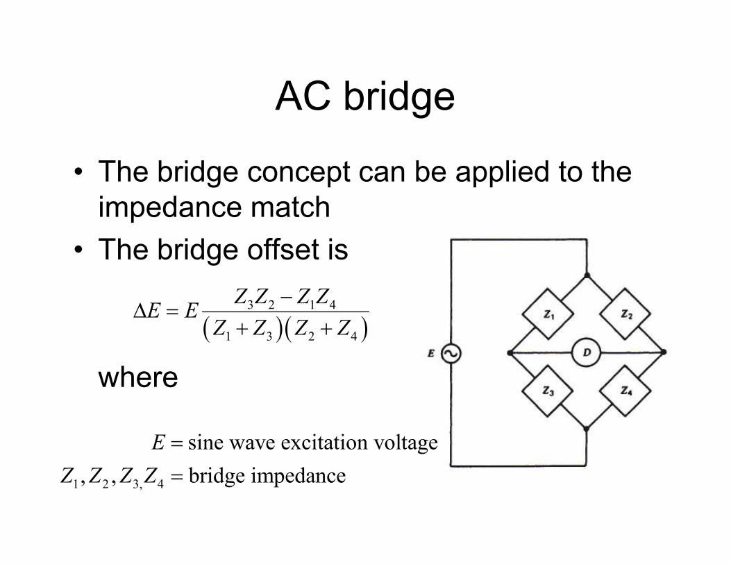
AC bridge
• The bridge concept can be applied to the
impedance match
• The bridge offset is
where
( )( )3 2 1 4
1 3 2 4
Z Z Z ZE E
Z Z Z Z
−∆ =
+ +
1 2 3, 4
sine wave excitation voltage
, , bridge impedance
E
Z Z Z Z
=
=
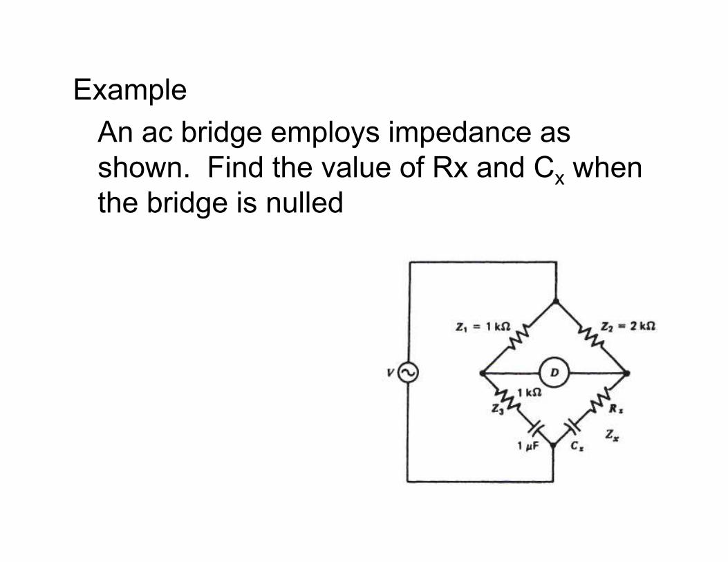
Example
An ac bridge employs impedance as
shown. Find the value of Rx and Cx when
the bridge is nulled
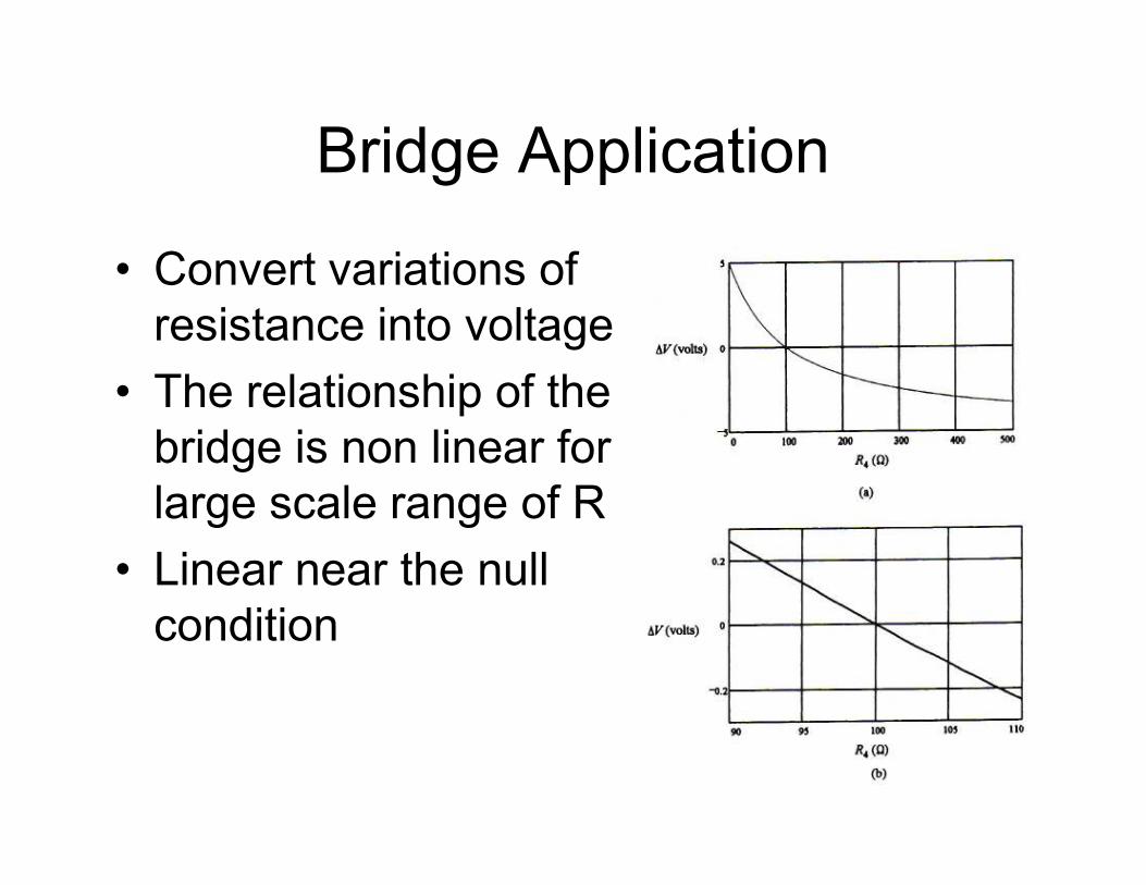
Bridge Application
• Convert variations of
resistance into voltage
• The relationship of the
bridge is non linear for bridge is non linear for
large scale range of R
• Linear near the null
condition
RC Filter
• To eliminate unwanted noise signals from
measurement, it is needed to use filter
circuit
A filter is a circuit that is
designed to pass signals
with desired frequencies
and reject or attenuate
others.
Filters
Background:
. Filters may be classified as either digital or analog.
. Digital filtersDigital filters are implemented using a digital . Digital filtersDigital filters are implemented using a digital
computer
or special purpose digital hardware.
. Analog filtersAnalog filters may be classified as either passive or
active and are usually implemented with R, L, and C
components and operational amplifiers.
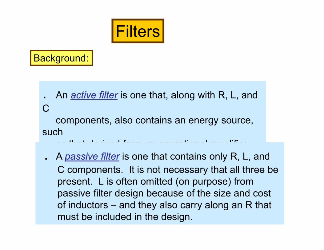
Filters
Background:
. An active filteractive filter is one that, along with R, L, and
C
components, also contains an energy source, components, also contains an energy source,
such
as that derived from an operational amplifier.
. A passive filterpassive filter is one that contains only R, L, and
C components. It is not necessary that all three be
present. L is often omitted (on purpose) from
passive filter design because of the size and cost
of inductors – and they also carry along an R that
must be included in the design.
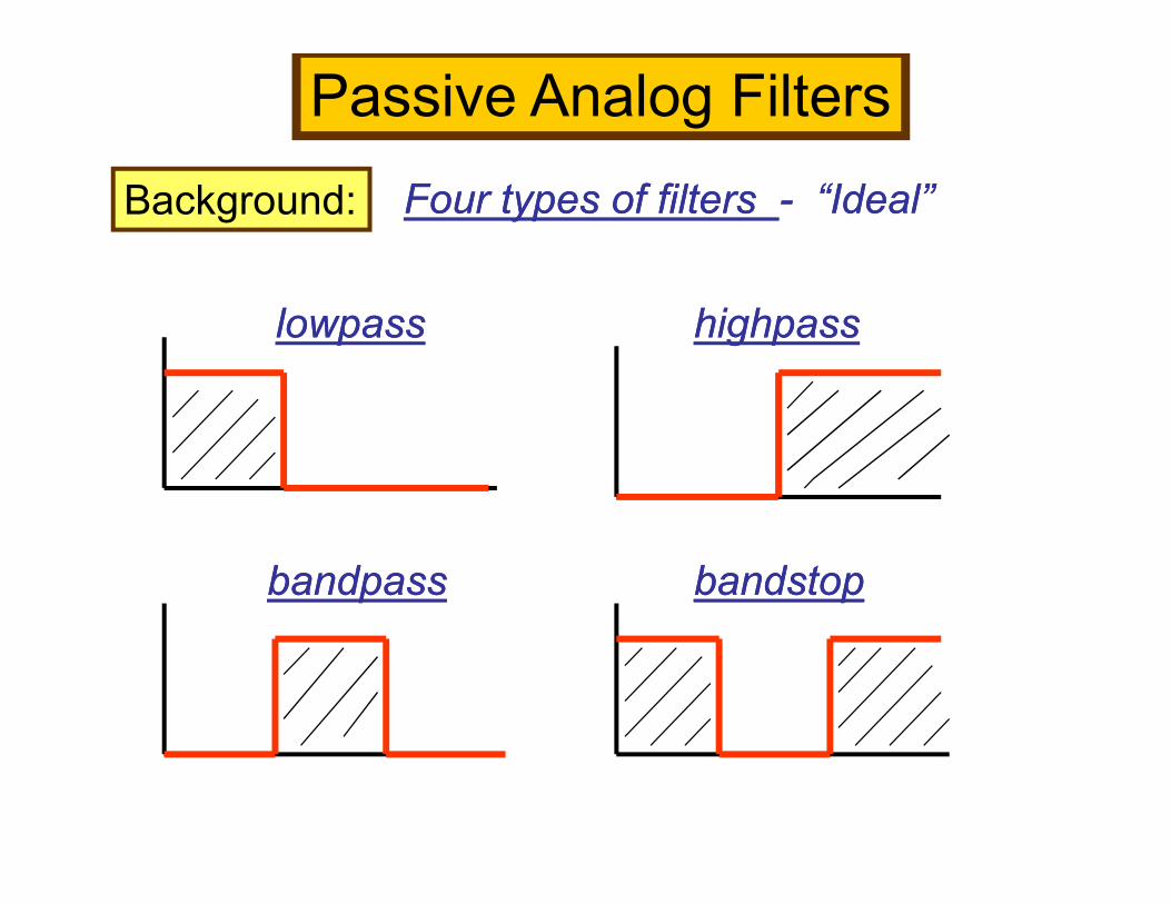
Passive Analog Filters
Background: Four types of filters Four types of filters -- “Ideal”“Ideal”
lowpasslowpass highpasshighpass
bandpassbandpass bandstopbandstop
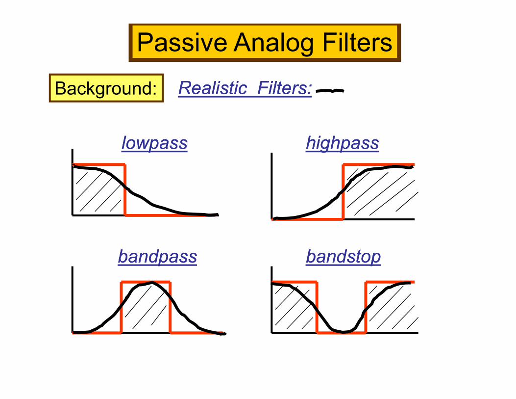
Background: Realistic Filters:Realistic Filters:
lowpasslowpass highpasshighpass
Passive Analog Filters
bandpassbandpass bandstopbandstop
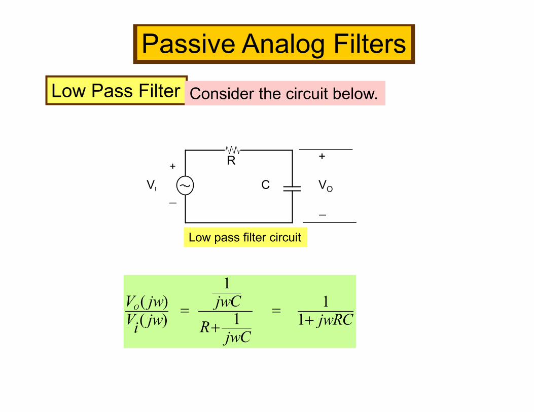
Passive Analog Filters
Low Pass Filter Consider the circuit below.
R
CVI VO
+
_
+
__
1( ) 1
1( ) 1OV jw jwCV jw jwRC
RijwC
= =++
Low pass filter circuit
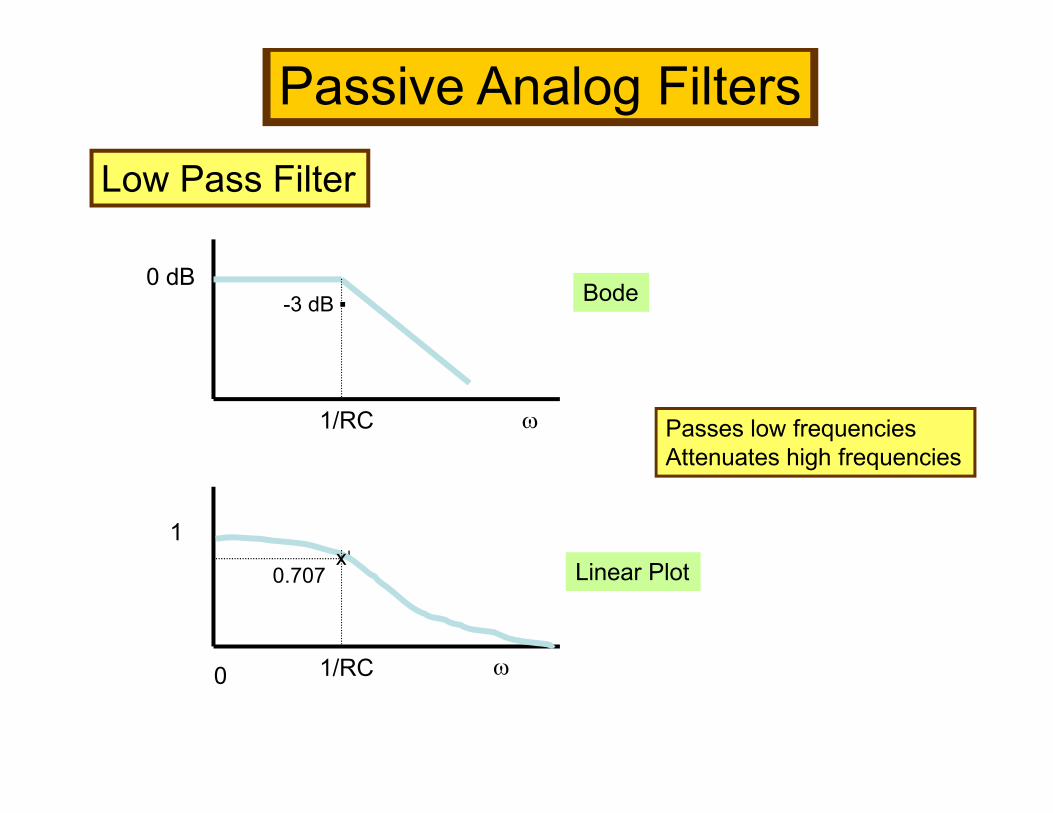
Passive Analog Filters
Low Pass Filter
0 dB
ω
Bode.-3 dB
1
ω
ω0
1/RC
1/RC
Linear Plotx
0.707
Passes low frequencies
Attenuates high frequencies
Passive Analog Filters
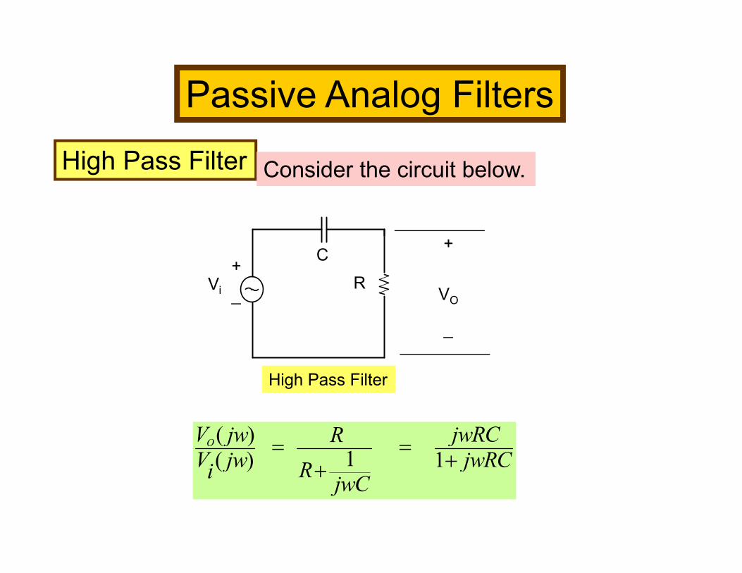
High Pass Filter Consider the circuit below.
C
RVi V
+
+
_RVi VO
_
_
( )1( ) 1
OV jw jwRCRV jw jwRC
RijwC
= =++
High Pass Filter
Passive Analog Filters
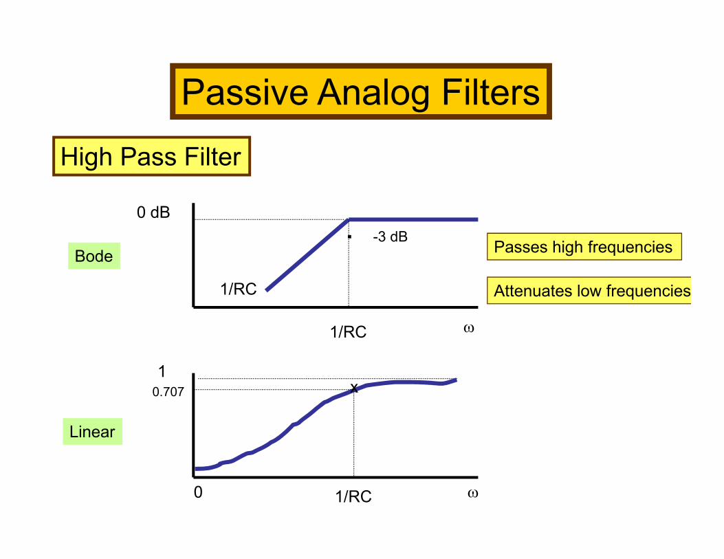
High Pass Filter
0 dB
. -3 dB
BodePasses high frequencies
.
0 ω
ω
1/RC
1/RC
1/RC
10.707
Linear
Attenuates low frequencies
x
Passive Analog Filters
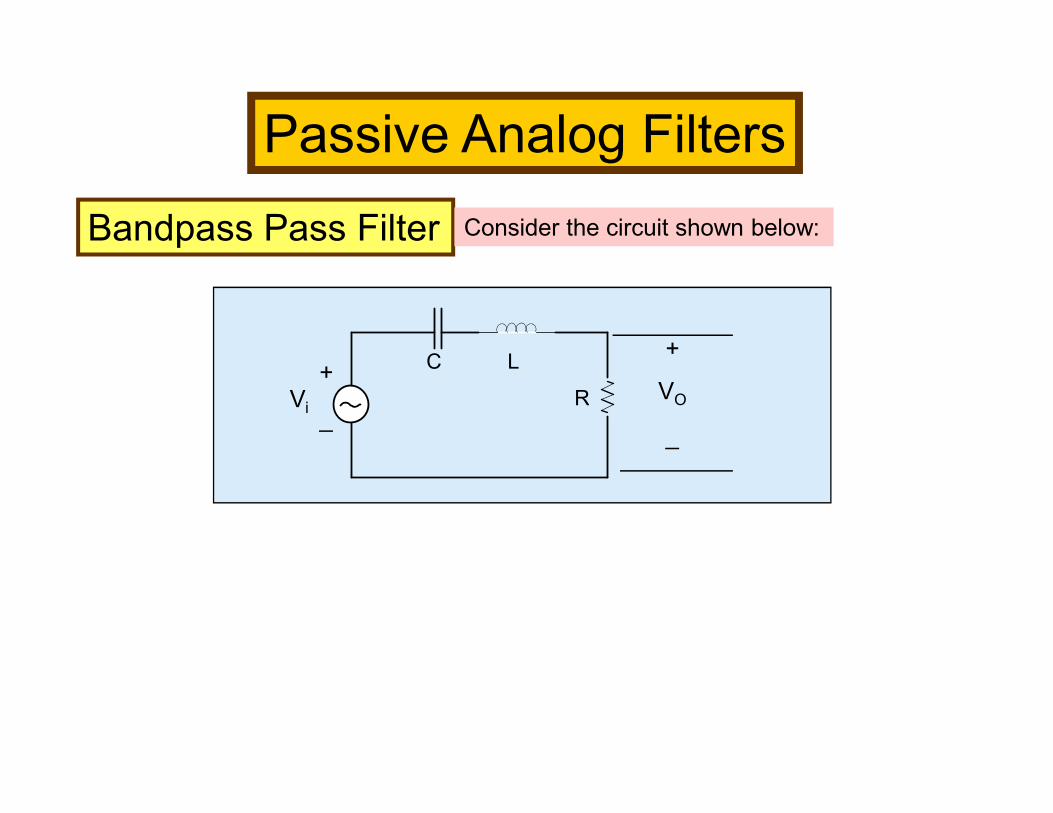
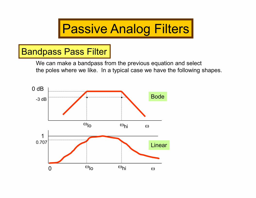
Bandpass Pass Filter Consider the circuit shown below:
C L
RViVO
++
_RVi
__
Passive Analog Filters
Bandpass Pass FilterWe can make a bandpass from the previous equation and select
the poles where we like. In a typical case we have the following shapes.
0 dB
-3 dB. . Bode
ω
ω0
-3 dB
ωlo
ωhi
.
. .
.10.707
Bode
Linear
ωlo
ωhi
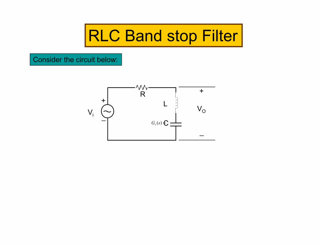
RLC Band stop Filter
Consider the circuit below:
R
L
C
+
VO
+
_Vi
=)(sGv C
_
=)(sGv
VinVO
C
Rfb
+
_
+
_
Rin
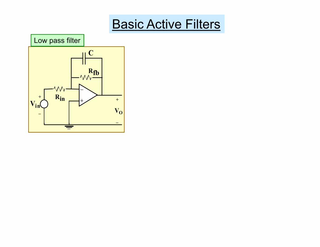
Basic Active FiltersLow pass filter
Basic Active Filters
RinC
Vin
Rfb
VO
+
_
+
_
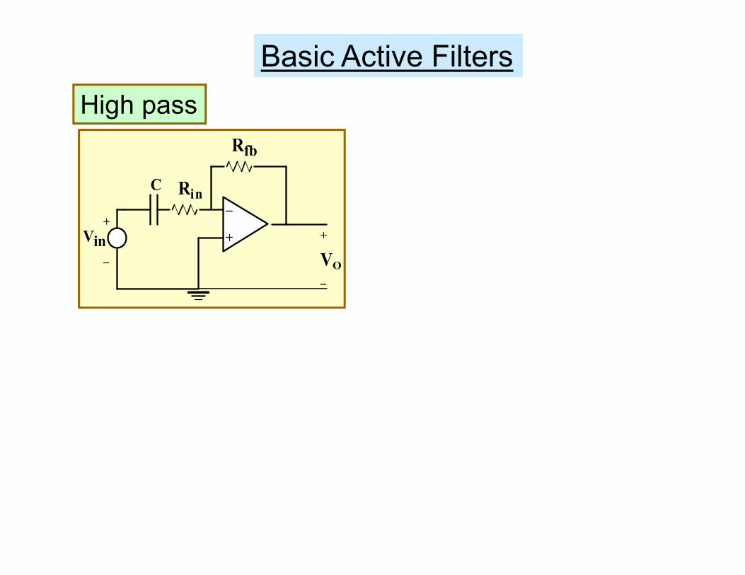
High pass
Basic Active Filters
Vin
R1
R1
C1
C2
R2R2
Rfb
Ri
V
+
+_
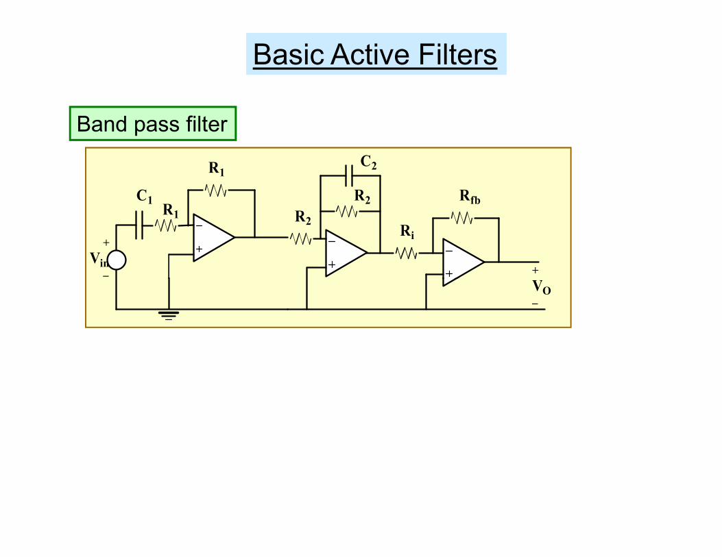
Band pass filter
VO_
Basic Active Filters
R1
R1
C1
Rfb
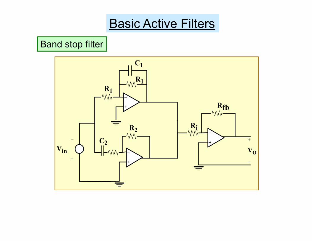
Band stop filter
Vin
C2
R2Ri
VO
+
_
+
_
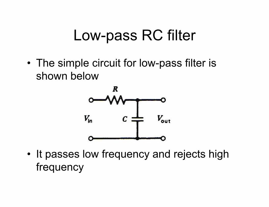
Low-pass RC filter
• The simple circuit for low-pass filter is
shown below
• It passes low frequency and rejects high
frequency
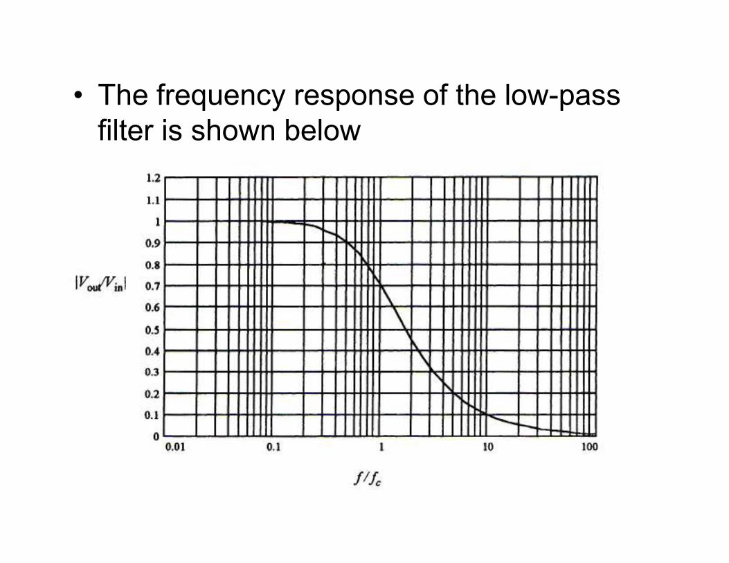
• The frequency response of the low-pass
filter is shown below
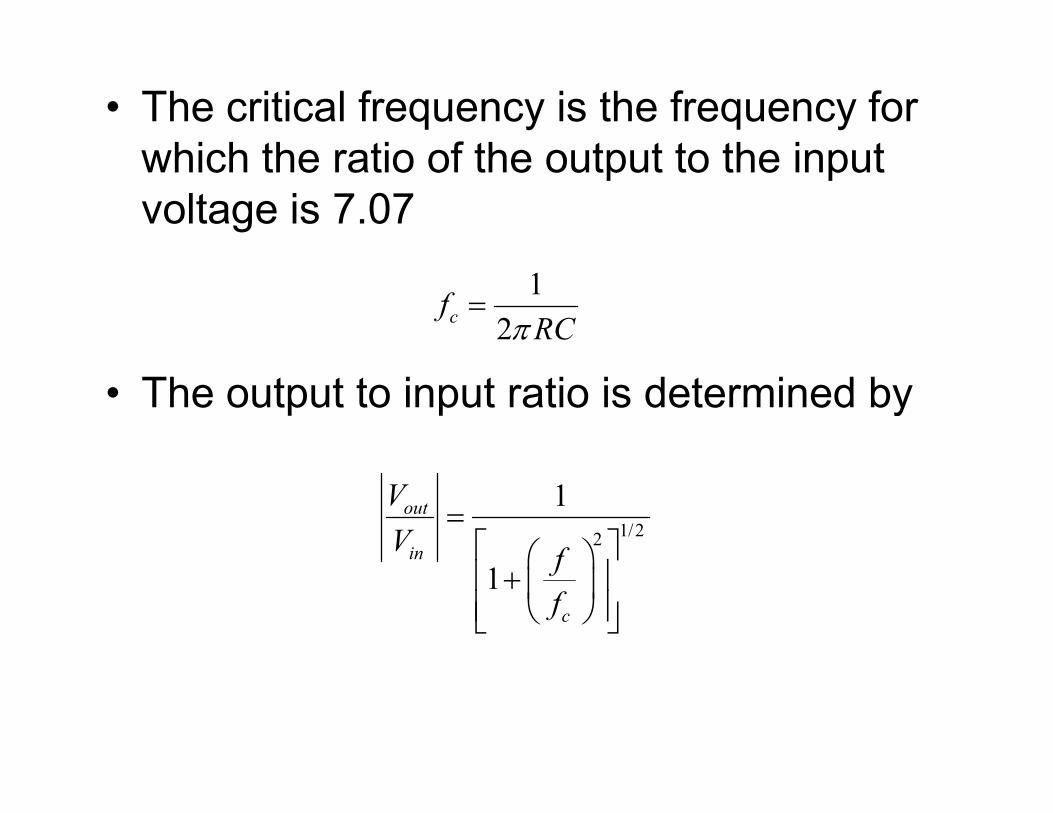
• The critical frequency is the frequency for
which the ratio of the output to the input
voltage is 7.07
• The output to input ratio is determined by
1
2cf
RCπ=
• The output to input ratio is determined by
1/22
1
1
out
in
c
V
Vf
f
= +
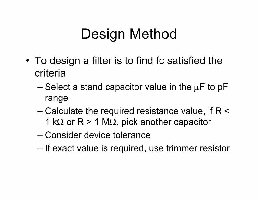
Design Method
• To design a filter is to find fc satisfied the
criteria
– Select a stand capacitor value in the µF to pF
rangerange
– Calculate the required resistance value, if R <
1 kΩ or R > 1 MΩ, pick another capacitor
– Consider device tolerance
– If exact value is required, use trimmer resistor
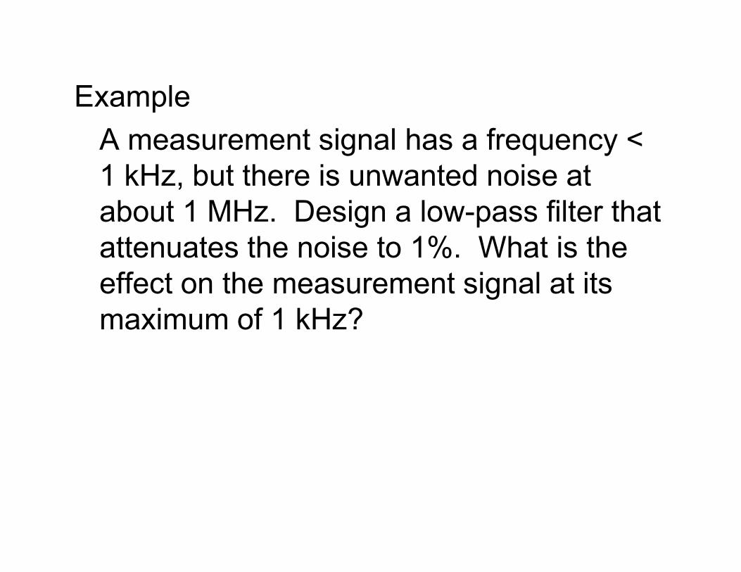
Example
A measurement signal has a frequency <
1 kHz, but there is unwanted noise at
about 1 MHz. Design a low-pass filter that
attenuates the noise to 1%. What is the
effect on the measurement signal at its effect on the measurement signal at its
maximum of 1 kHz?
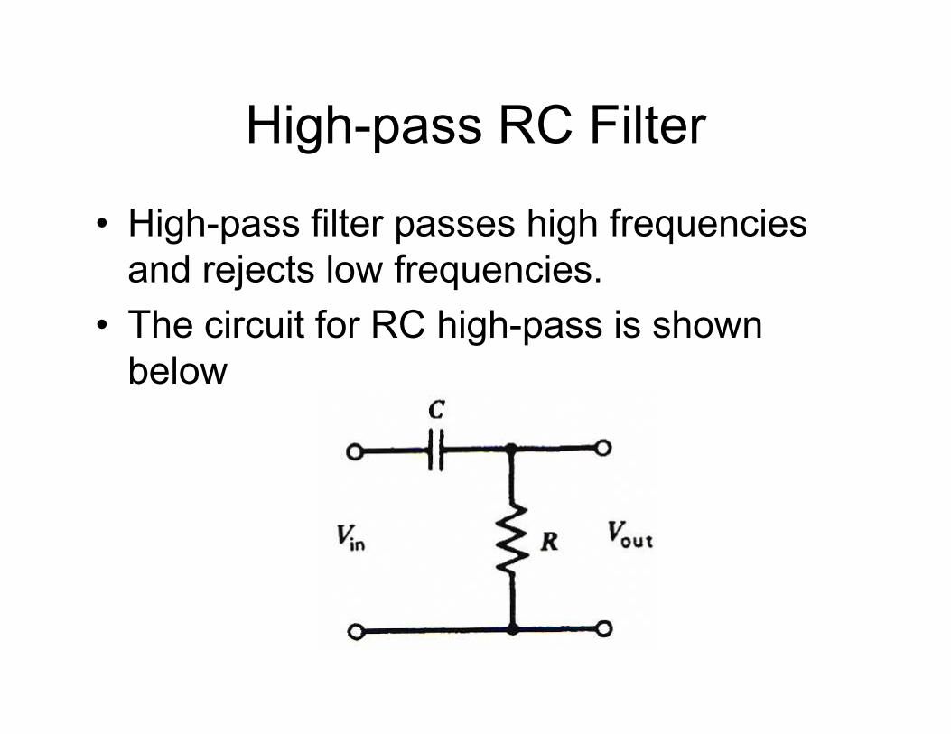
High-pass RC Filter
• High-pass filter passes high frequencies
and rejects low frequencies.
• The circuit for RC high-pass is shown
belowbelow
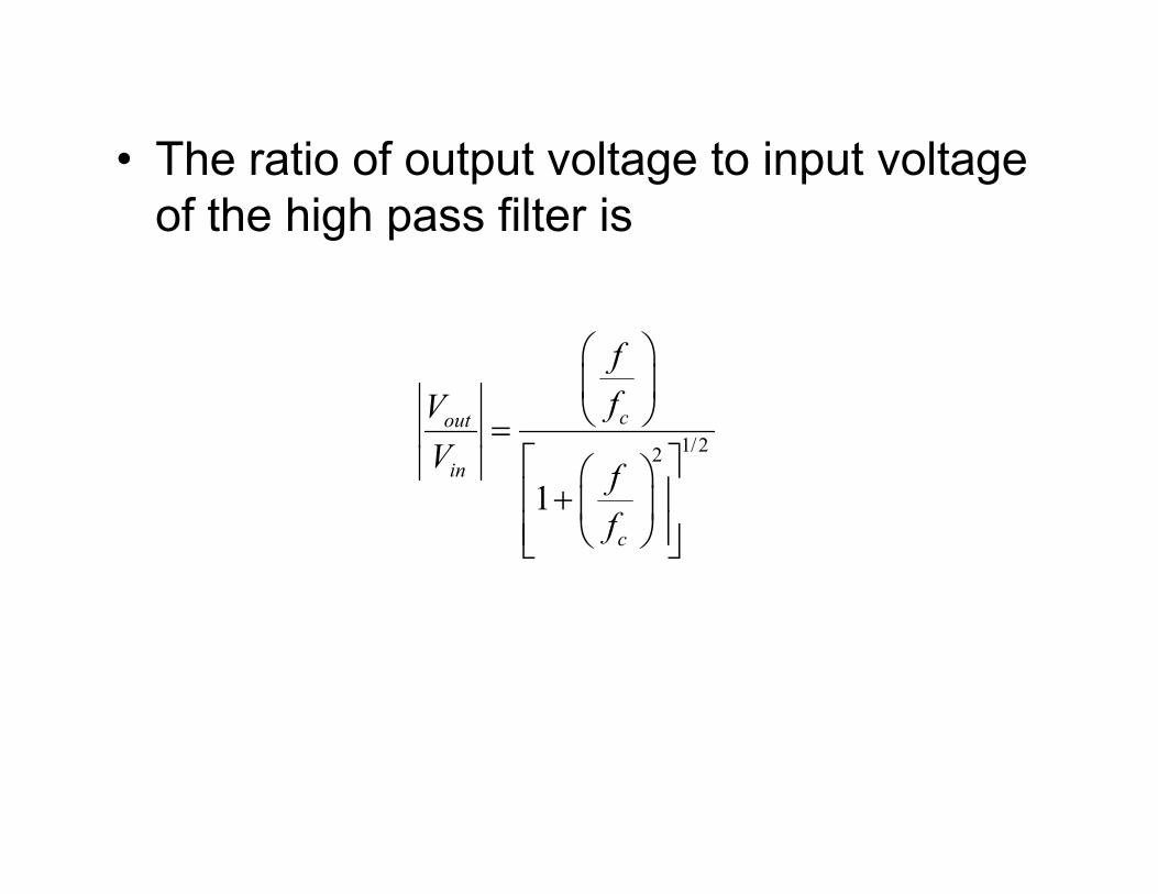
• The ratio of output voltage to input voltage
of the high pass filter is
1/22
cout
f
fV
V
=
1/2
2
1in
c
Vf
f
= +
Example 2.12
Pulses for a stepping motor are being
transmitted at 2000 Hz. Design a filter to
reduce 60 Hz noise but reduce the pulses
by no more than 3 dB.
RC Filter Consideration
• Very small resistance should be avoided because
it can lead to large current and loading effect
• If input impedance of the circuit fed by the filter is
low, a voltage follower circuit is neededlow, a voltage follower circuit is needed
• The output impedance of the filter must be much
less than the input impedance of the next stage
circuit
Example
A 2 kHz data signal is contaminated by 60
Hz of noise. Compare a single-stage and
a two stage high-pass RC filter for
reducing the noise by 60 dB. What effect
does each have on the data signal?does each have on the data signal?
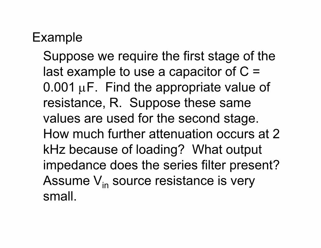
Example
Suppose we require the first stage of the
last example to use a capacitor of C =
0.001 µF. Find the appropriate value of
resistance, R. Suppose these same
values are used for the second stage. values are used for the second stage.
How much further attenuation occurs at 2
kHz because of loading? What output
impedance does the series filter present?
Assume Vin source resistance is very
small.
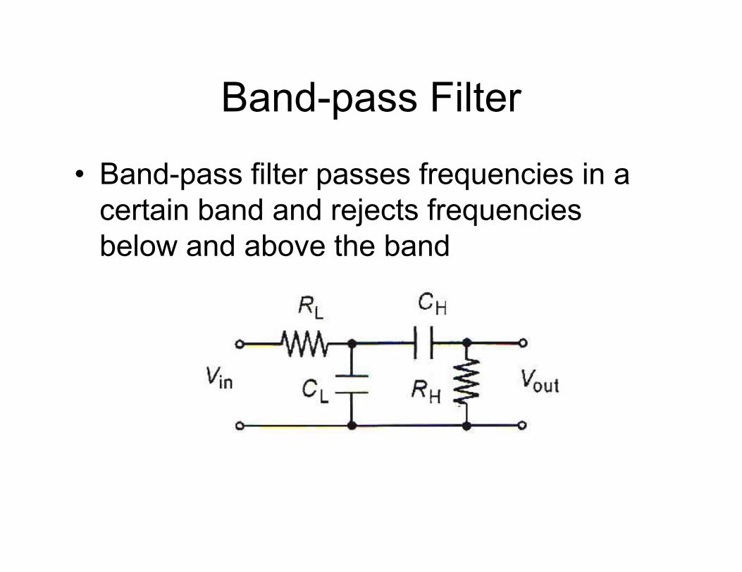
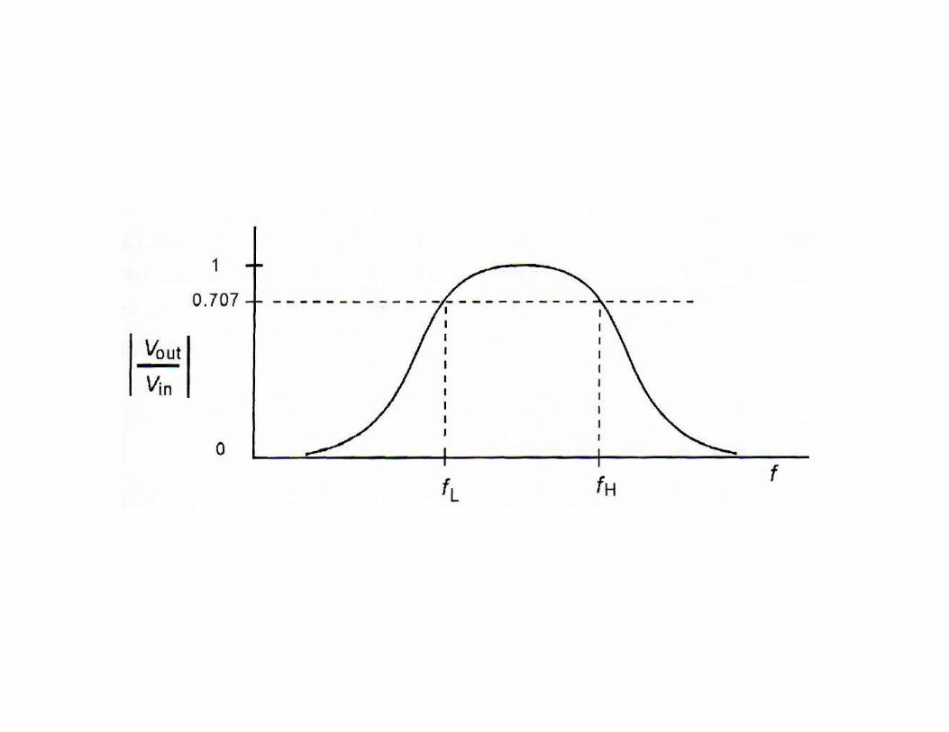
Band-pass Filter
• Band-pass filter passes frequencies in a
certain band and rejects frequencies
below and above the band
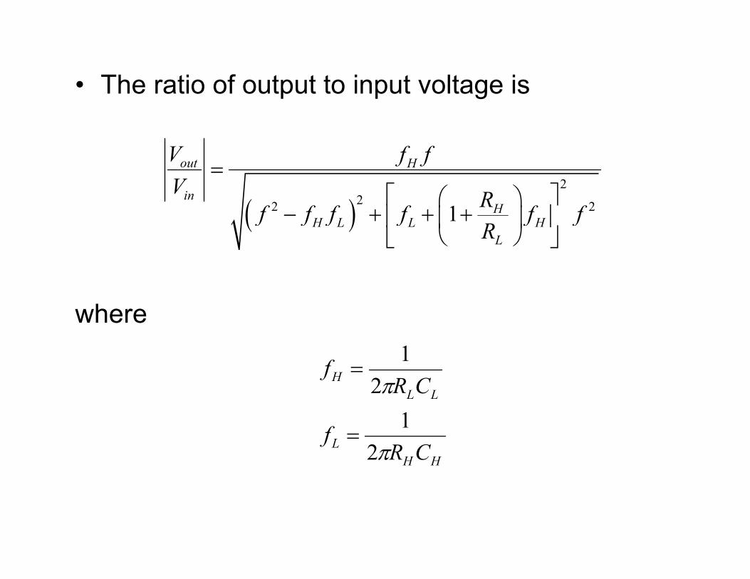
• The ratio of output to input voltage is
( )2
22 21
out H
inH
H L L H
L
V f f
VR
f f f f f fR
=
− + + +
where
HH
L
LL
H
CRf
CRf
π
π
2
1
2
1
=
=
Example
A signal-conditioning system uses a
frequency variation from 6 kHz to 60 kHz
to carry measurement information. There
is considerable noise at 120 Hz and at 1
MHz. Design a band-pass filter to reduce
the noise by 90%. What is the effect on
the desired passband frequency.
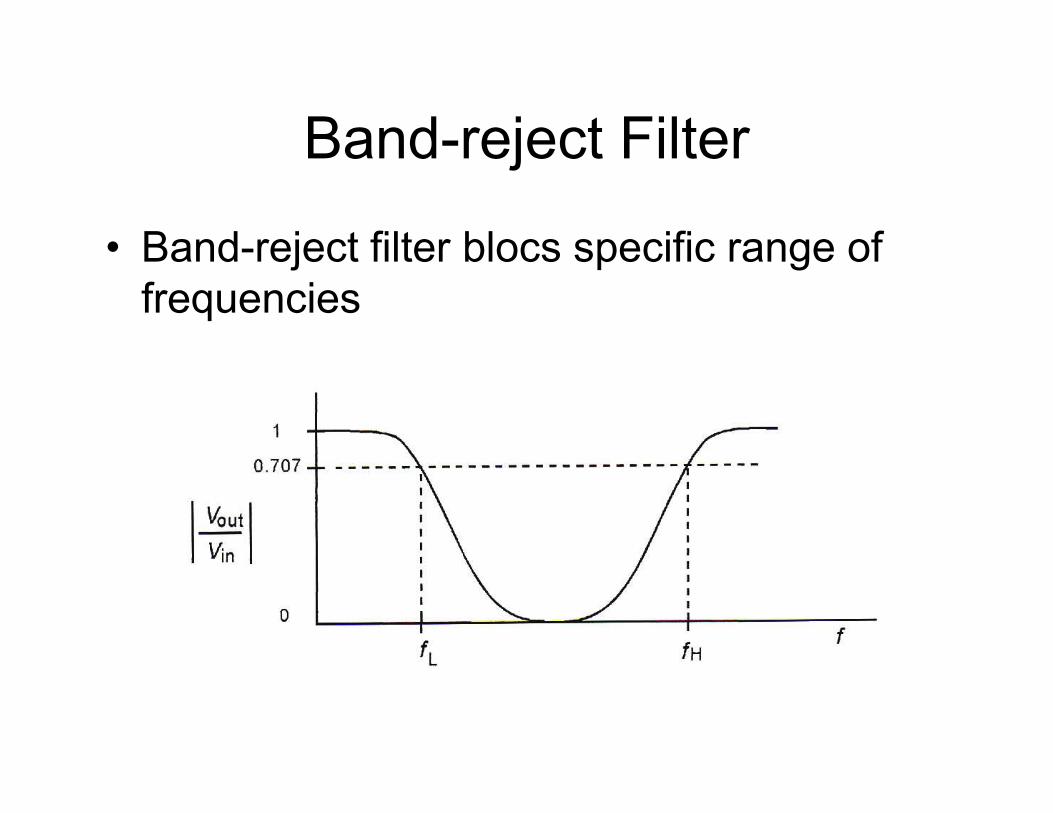
Band-reject Filter
• Band-reject filter blocs specific range of
frequencies
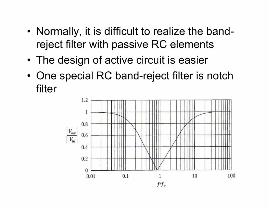
• Normally, it is difficult to realize the band-
reject filter with passive RC elements
• The design of active circuit is easier
• One special RC band-reject filter is notch
filter
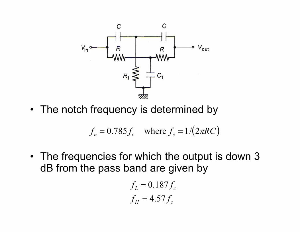
• The notch frequency is determined by
• The frequencies for which the output is down 3 dB from the pass band are given by
( )RCfff ccn π2/1 where785.0 ==
cH
cL
ff
ff
57.4
187.0
=
=
Example
A frequency of 400 Hz prevails aboard an
aircraft. Design a twin-T notch filter to
reduce the 400 Hz signal. What effect
would this have on voice signal at 10 to
300 Hz? At what higher frequency is the 300 Hz? At what higher frequency is the
output down by 3 dB
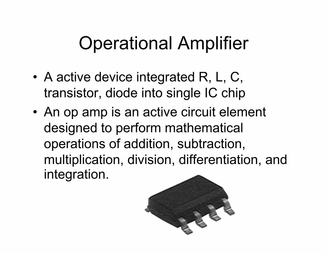
Operational Amplifier
• A active device integrated R, L, C,
transistor, diode into single IC chip
• An op amp is an active circuit element
designed to perform mathematical designed to perform mathematical
operations of addition, subtraction,
multiplication, division, differentiation, and integration.
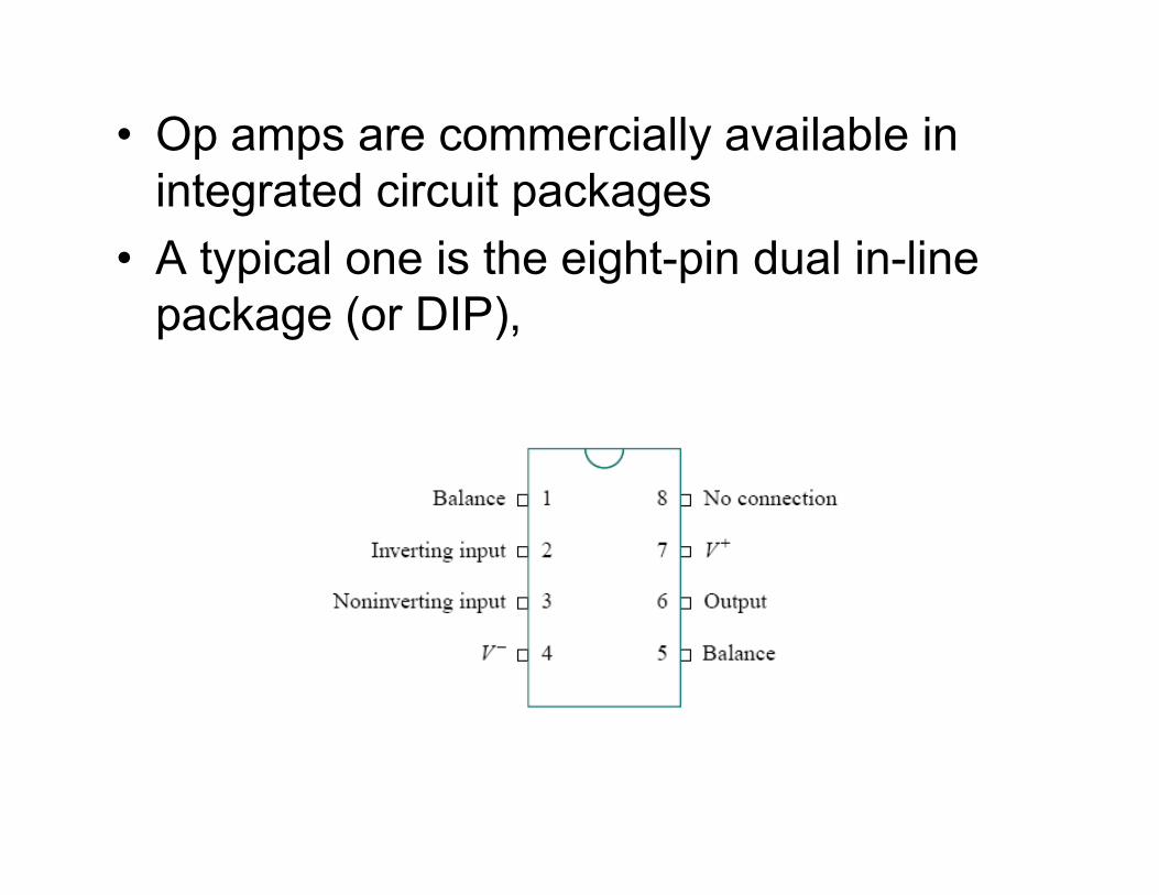
• Op amps are commercially available in
integrated circuit packages
• A typical one is the eight-pin dual in-line
package (or DIP),
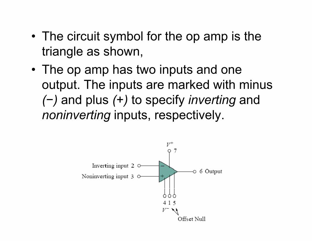
• The circuit symbol for the op amp is the
triangle as shown,
• The op amp has two inputs and one
output. The inputs are marked with minus
(−) and plus (+) to specify inverting and
noninverting inputs, respectively. noninverting inputs, respectively.
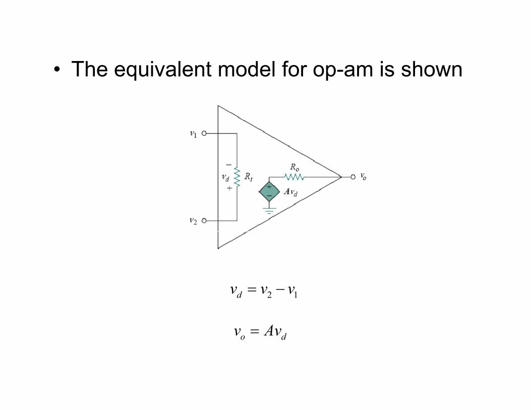
• The equivalent model for op-am is shown
2 1dv v v= −
o dv Av=
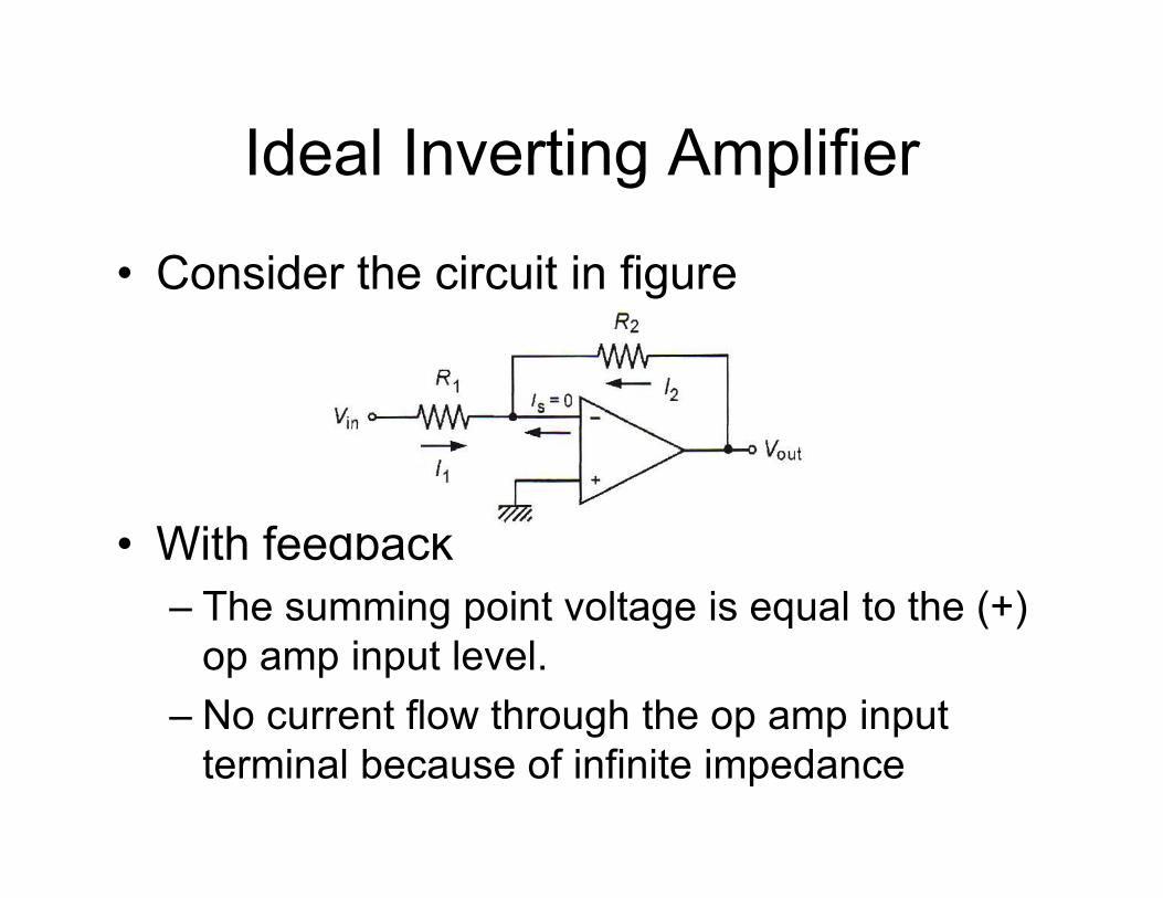
Ideal Inverting Amplifier
• Consider the circuit in figure
• With feedback
– The summing point voltage is equal to the (+)
op amp input level.
– No current flow through the op amp input
terminal because of infinite impedance
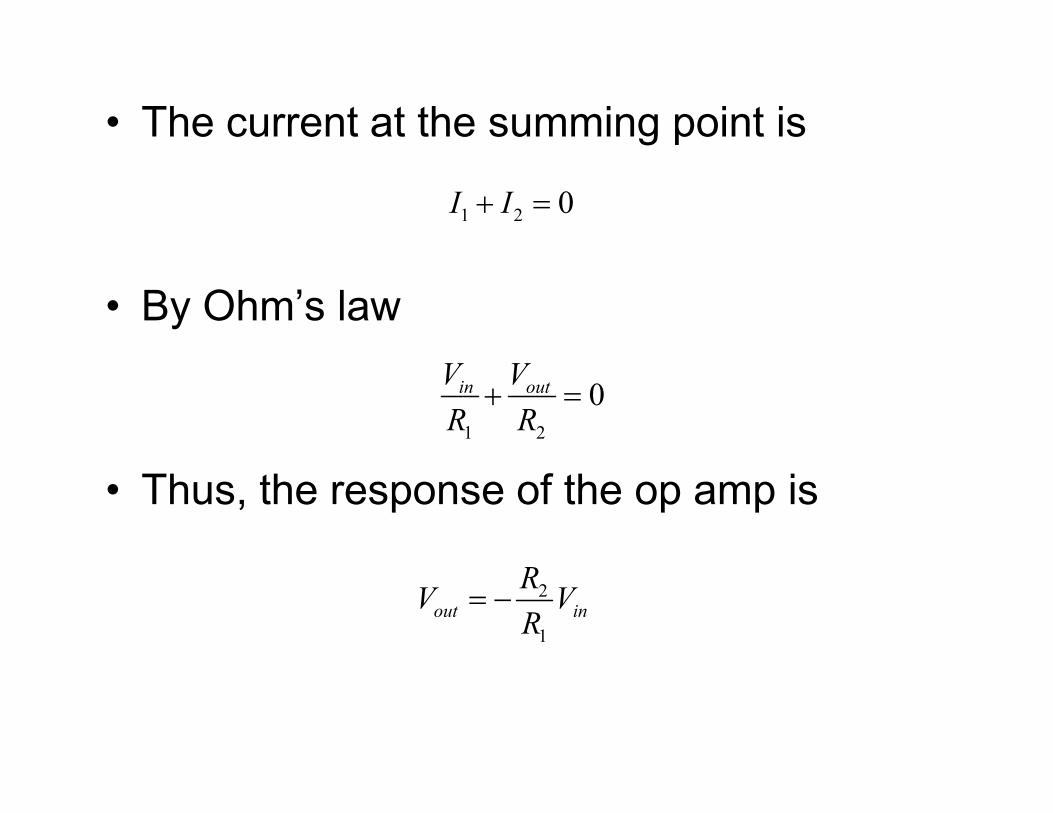
• The current at the summing point is
• By Ohm’s law
1 2 0I I+ =
0in outV V
R R+ =
• Thus, the response of the op amp is
1 2
0R R+ =
2
1
out in
RV V
R= −
Design Rules
• Rule 1 Assume that no current flows
through the op amp input terminals – that
is, the inverting and noninverting terminals
• Assume that there is no voltage difference • Assume that there is no voltage difference
between the op amp input terminals
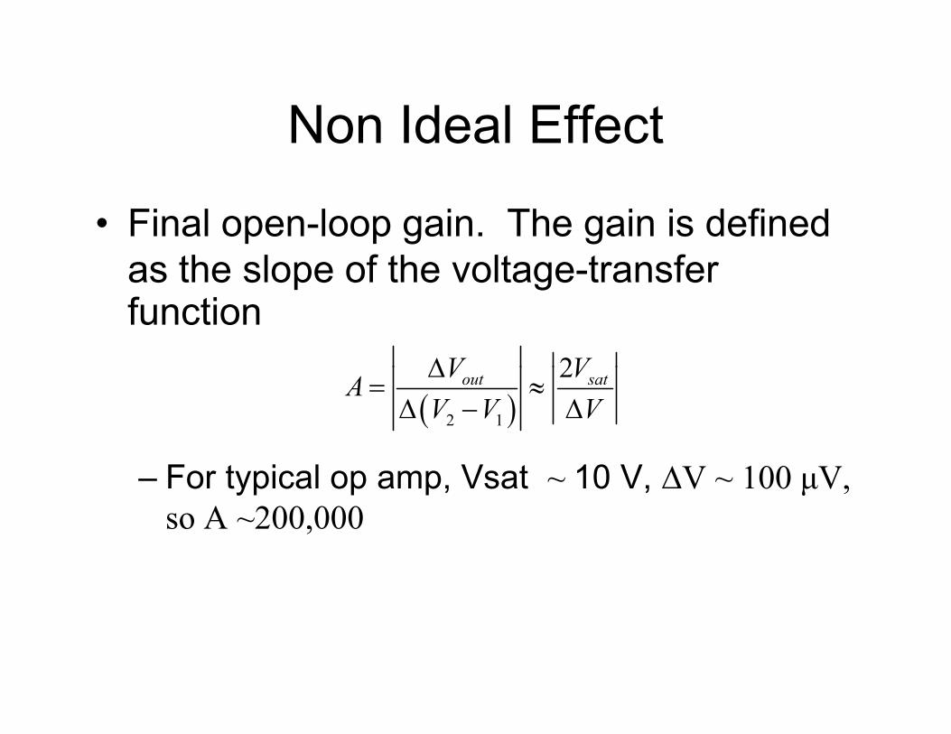
Non Ideal Effect
• Final open-loop gain. The gain is defined
as the slope of the voltage-transfer function
2V V∆= ≈
– For typical op amp, Vsat ~ 10 V, ∆V ~ 100 µV,
so A ~200,000
( )2 1
2out satV VA
V V V
∆= ≈∆ − ∆
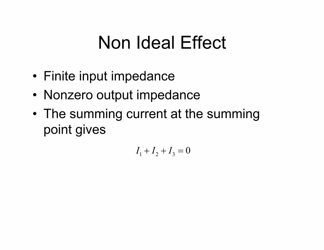
Non Ideal Effect
• Finite input impedance
• Nonzero output impedance
• The summing current at the summing
point givespoint gives
1 2 3 0I I I+ + =
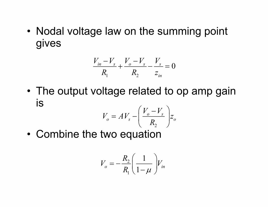
• Nodal voltage law on the summing point gives
• The output voltage related to op amp gain is
1 2
0in s o s s
in
V V V V V
R R z
− −+ − =
is
• Combine the two equation2
o so s o
V VV AV z
R
−= −
2
1
1
1o in
RV V
R µ
= − −
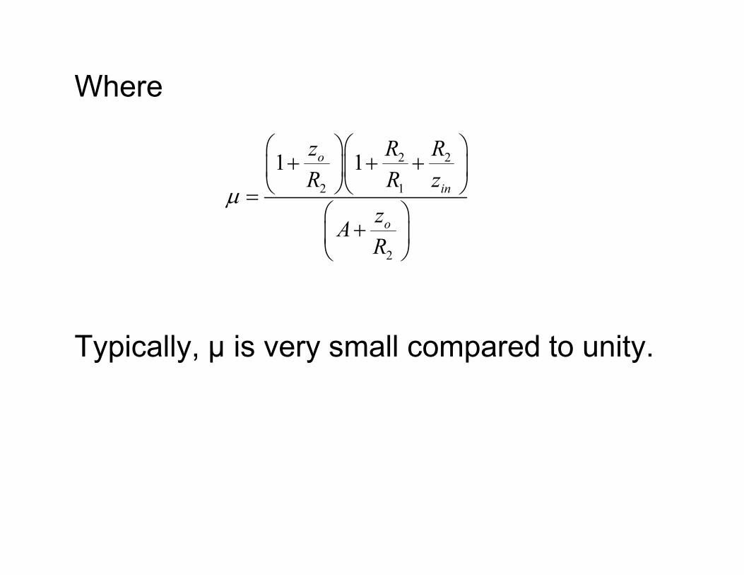
Where
2 2
2 1
2
1 1o
in
o
z R R
R R z
zAR
µ
+ + +
=
+
Typically, µ is very small compared to unity.
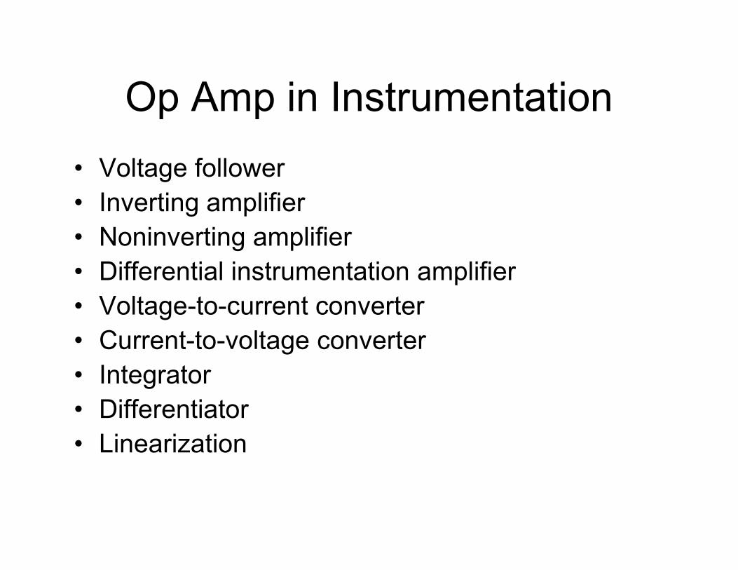
Op Amp in Instrumentation
• Voltage follower
• Inverting amplifier
• Noninverting amplifier
• Differential instrumentation amplifier• Differential instrumentation amplifier
• Voltage-to-current converter
• Current-to-voltage converter
• Integrator
• Differentiator
• Linearization
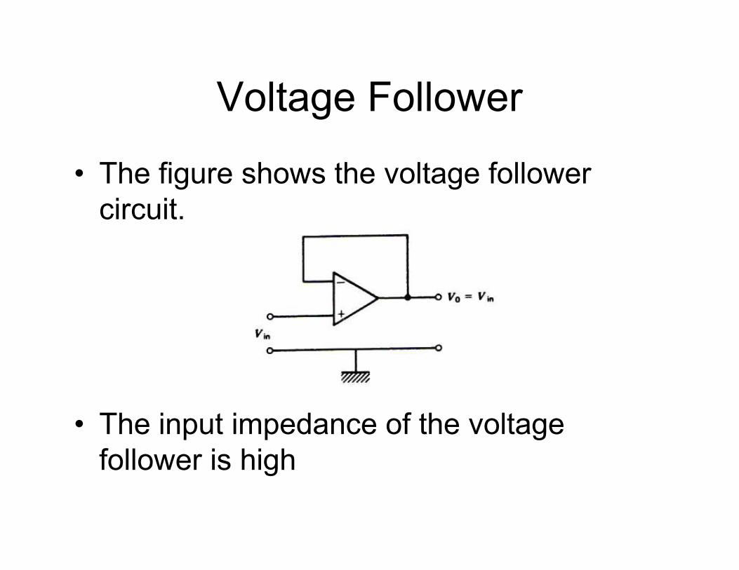
Voltage Follower
• The figure shows the voltage follower
circuit.
• The input impedance of the voltage
follower is high
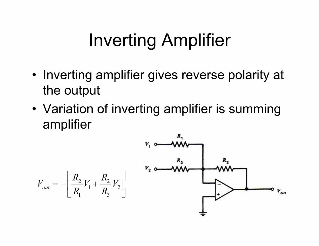
Inverting Amplifier
• Inverting amplifier gives reverse polarity at
the output
• Variation of inverting amplifier is summing
amplifier amplifier
2 21 2
1 3
out
R RV V V
R R
= − +
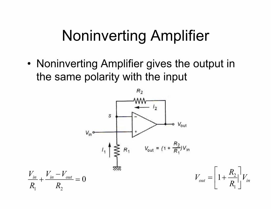
Noninverting Amplifier
• Noninverting Amplifier gives the output in
the same polarity with the input
1 2
0in in outV V V
R R
−+ =
2
1
1out in
RV V
R
= +
Example
Design a high-impedance amplifier with a
voltage gain of 42.
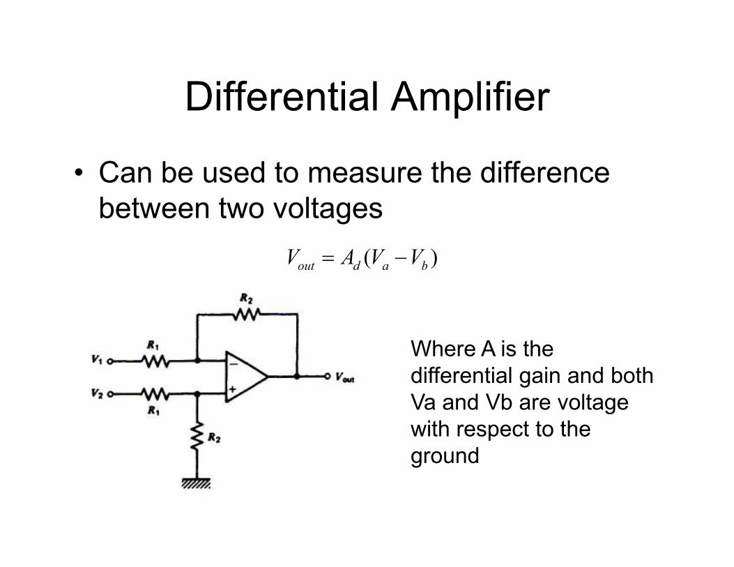
Differential Amplifier
• Can be used to measure the difference
between two voltages
( )out d a bV A V V= −
Where A is the
differential gain and both
Va and Vb are voltage
with respect to the
ground
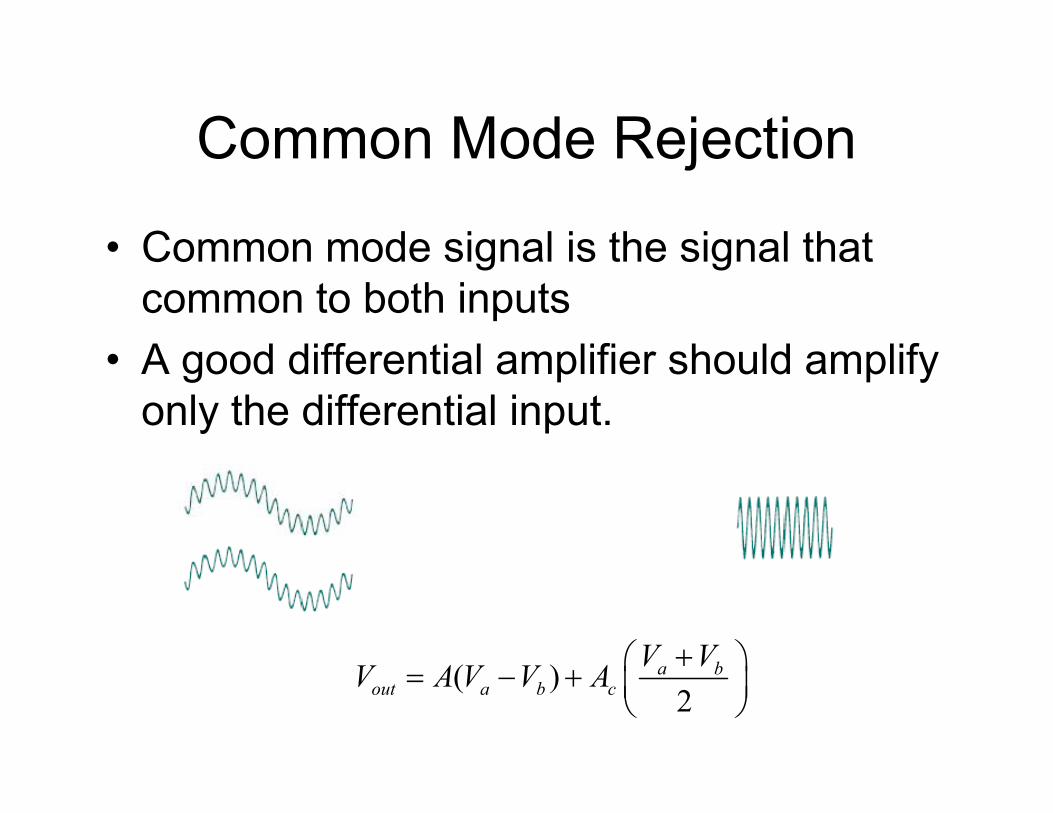
Common Mode Rejection
• Common mode signal is the signal that
common to both inputs
• A good differential amplifier should amplify
only the differential input.only the differential input.
( )2
a bout a b c
V VV A V V A
+ = − +
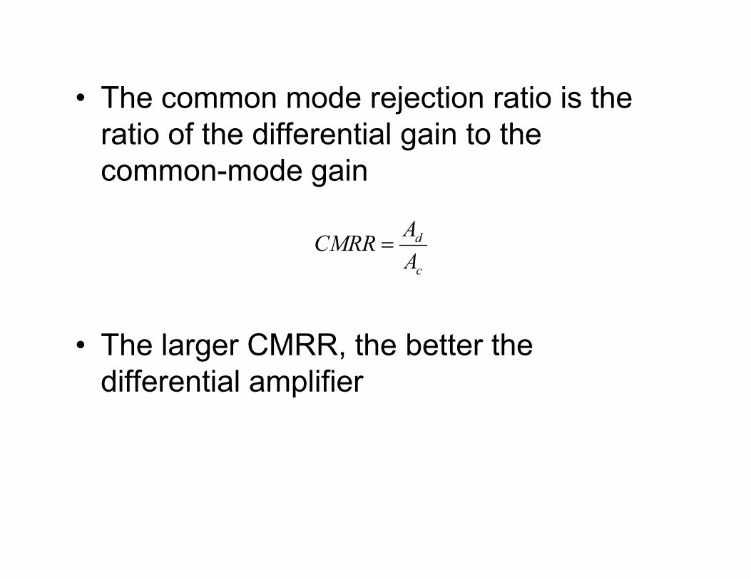
• The common mode rejection ratio is the
ratio of the differential gain to the
common-mode gain
d
c
ACMRR
A=
• The larger CMRR, the better the
differential amplifier
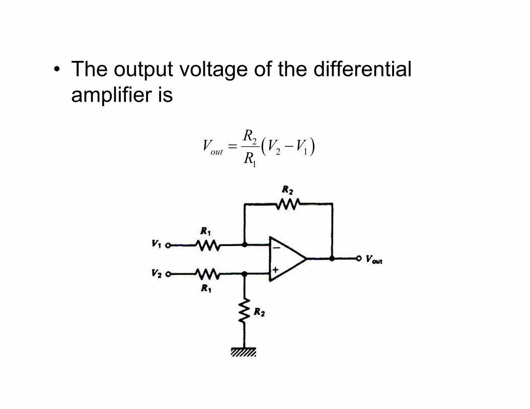
• The output voltage of the differential
amplifier is
( )22 1
1
out
RV V V
R= −
Example
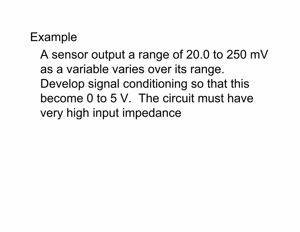
A sensor output a range of 20.0 to 250 mV
as a variable varies over its range.
Develop signal conditioning so that this
become 0 to 5 V. The circuit must have
very high input impedancevery high input impedance
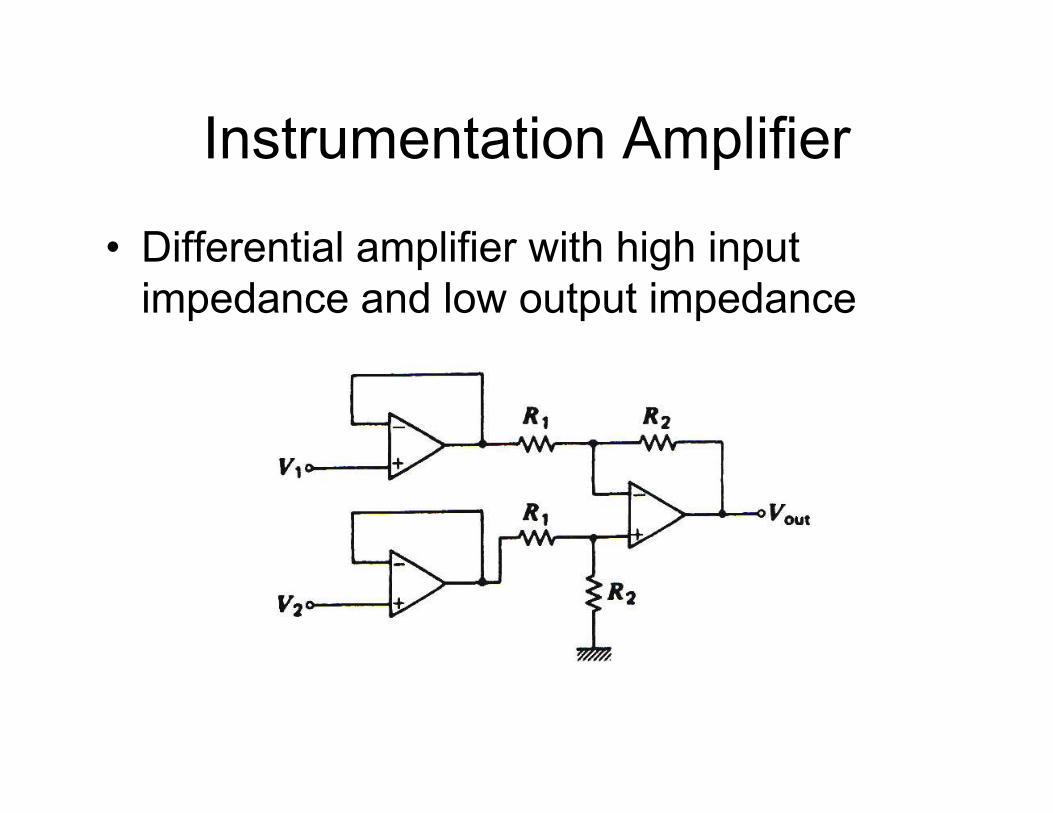
Instrumentation Amplifier
• Differential amplifier with high input
impedance and low output impedance
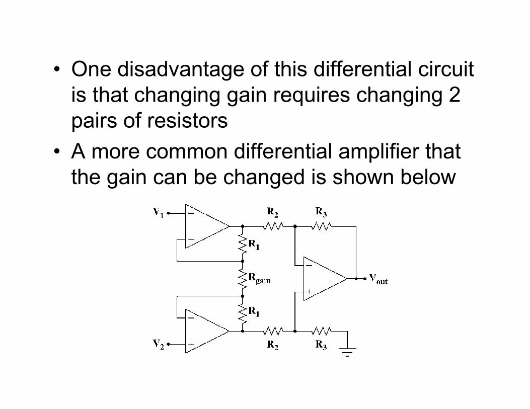
• One disadvantage of this differential circuit
is that changing gain requires changing 2
pairs of resistors
• A more common differential amplifier that
the gain can be changed is shown below
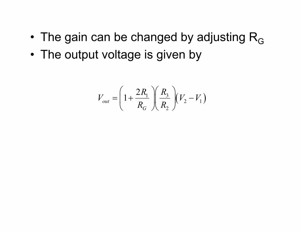
• The gain can be changed by adjusting RG
• The output voltage is given by
( )312 1
2
21out
G
RRV V V
R R
= + −
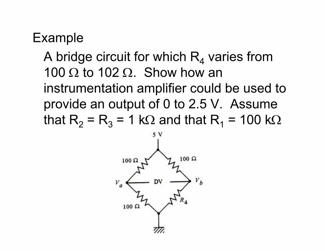
Example
A bridge circuit for which R4 varies from
100 Ω to 102 Ω. Show how an
instrumentation amplifier could be used to
provide an output of 0 to 2.5 V. Assume
that R2 = R3 = 1 kΩ and that R1 = 100 kΩthat R2 = R3 = 1 kΩ and that R1 = 100 kΩ
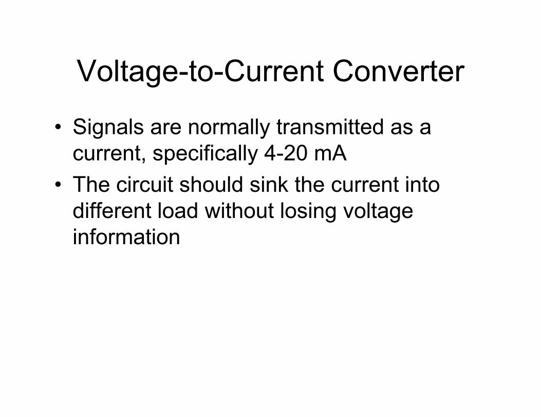
Voltage-to-Current Converter
• Signals are normally transmitted as a
current, specifically 4-20 mA
• The circuit should sink the current into
different load without losing voltage different load without losing voltage
information
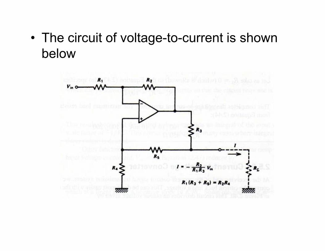
• The circuit of voltage-to-current is shown
below
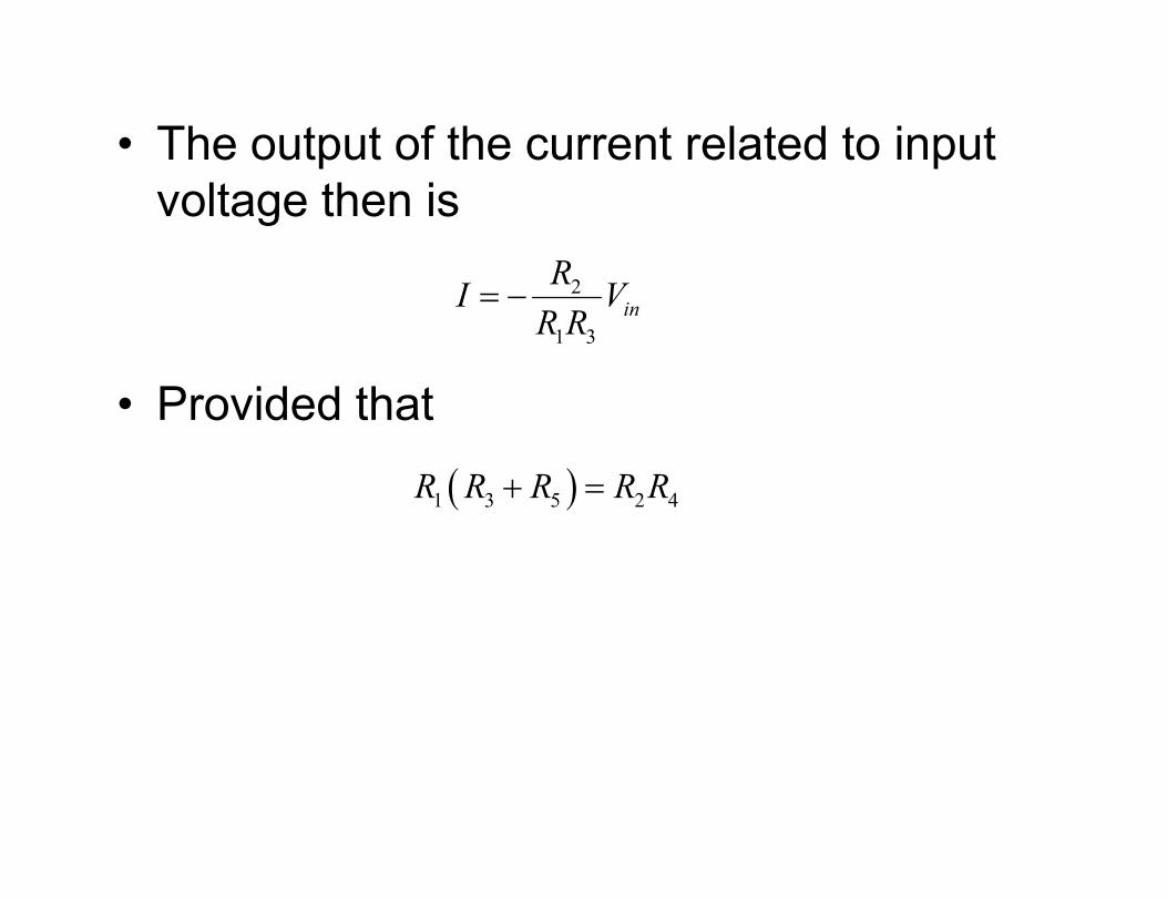
• The output of the current related to input
voltage then is
• Provided that
2
1 3
in
RI V
R R= −
( )1 3 5 2 4R R R R R+ =
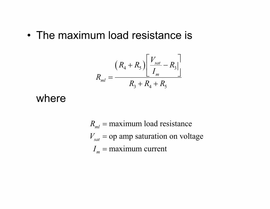
• The maximum load resistance is
where
( )4 5 3
3 4 5
sat
m
ml
VR R R
IR
R R R
+ −
=+ +
maximum load resistance
op amp saturation on voltage
maximum current
ml
sat
m
R
V
I
=
=
=
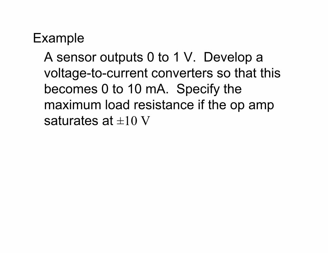
Example
A sensor outputs 0 to 1 V. Develop a
voltage-to-current converters so that this
becomes 0 to 10 mA. Specify the
maximum load resistance if the op amp
saturates at ±10 Vsaturates at ±10 V
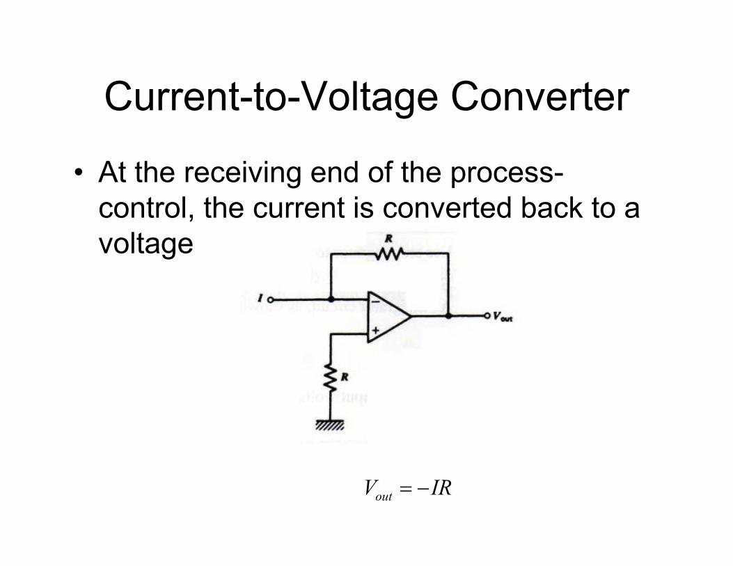
Current-to-Voltage Converter
• At the receiving end of the process-
control, the current is converted back to a
voltage
outV IR= −
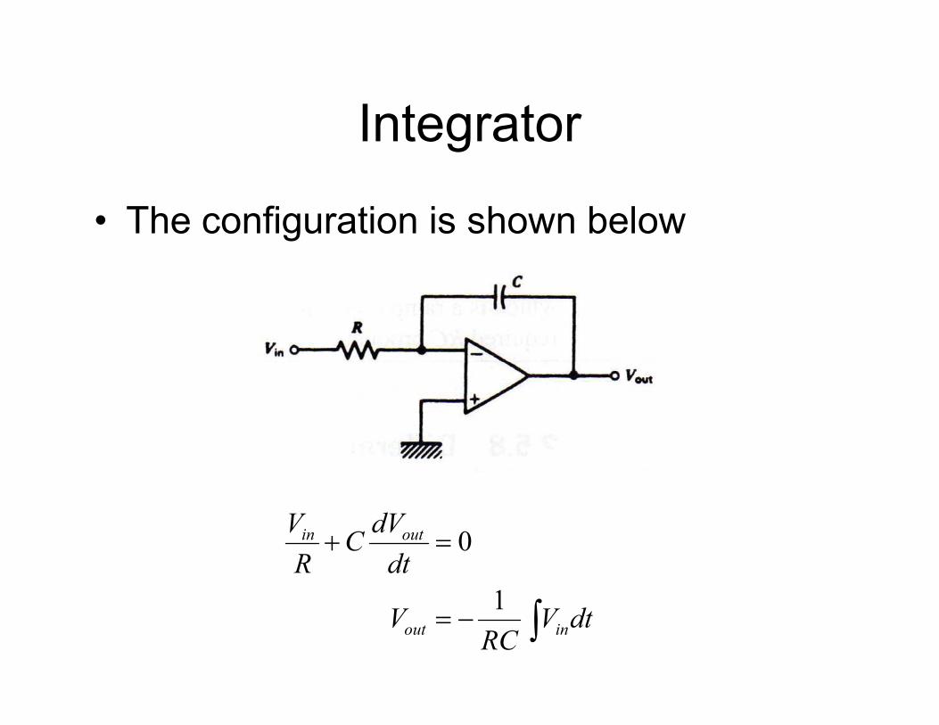
Integrator
• The configuration is shown below
0
1
in out
out in
V dVC
R dt
V V dtRC
+ =
= − ∫
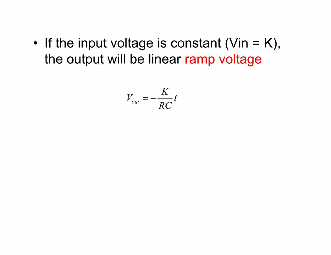
• If the input voltage is constant (Vin = K),
the output will be linear ramp voltage
out
KV t
RC= −
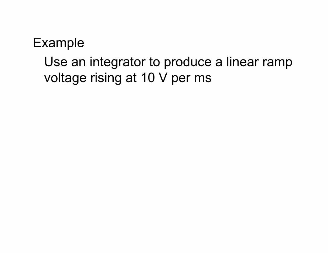
Example
Use an integrator to produce a linear ramp
voltage rising at 10 V per ms
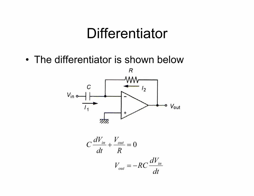
Differentiator
• The differentiator is shown below
0in out
inout
dV VCdt R
dVV RC
dt
+ =
= −
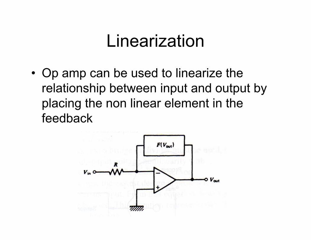
Linearization
• Op amp can be used to linearize the
relationship between input and output by
placing the non linear element in the
feedbackfeedback
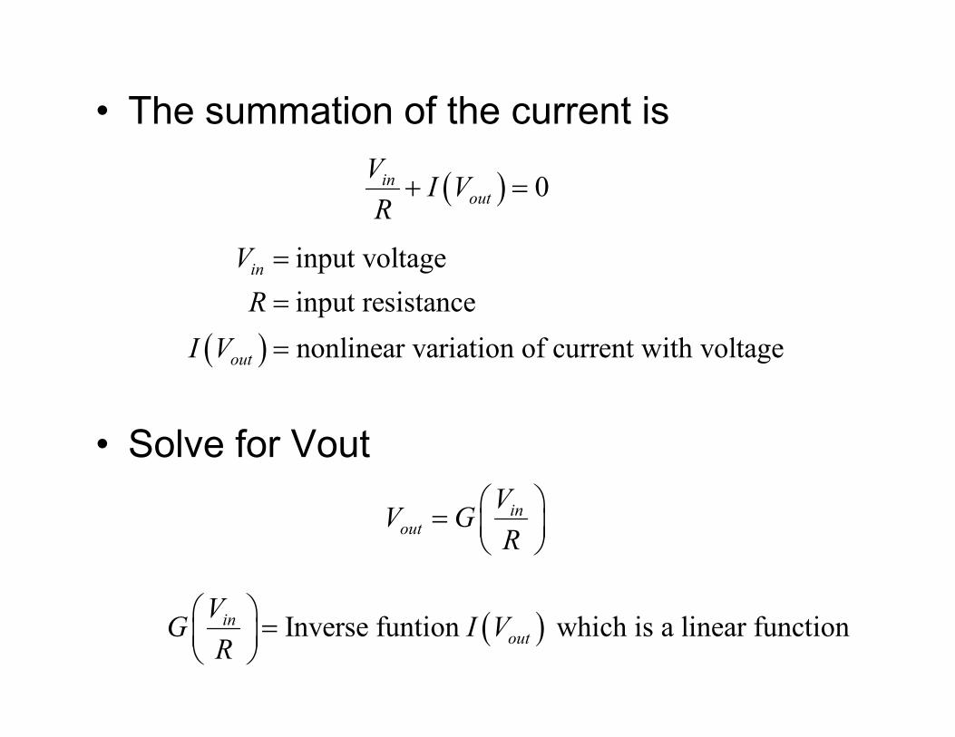
• The summation of the current is
( ) 0inout
VI V
R+ =
( )
input voltage
input resistance
nonlinear variation of current with voltage
in
out
V
R
I V
=
=
=
• Solve for Vout
inout
VV G
R
=
( )Inverse funtion which is a linear functioninout
VG I V
R
=
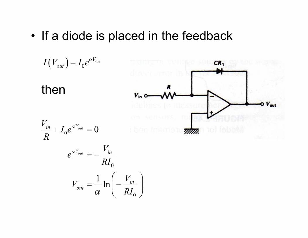
• If a diode is placed in the feedback
then
( ) 0outV
outI V I eα=
V0
0
0
0
1ln
out
out
Vin
V in
inout
VI e
R
Ve
RI
VV
RI
α
α
α
+ =
= −
= −


![[OPAMP] Analog Devices - Practical Design Techniques for Sensor Signal Conditioning](https://static.fdocuments.in/doc/165x107/552701bf550346f0358b4610/opamp-analog-devices-practical-design-techniques-for-sensor-signal-conditioning.jpg)


