by G. K. Miller - USGS · 2010-11-09 · regulation, system timing, system monitoring, analog...
94
UNITED STATES DEPARTMENT OF INTERIOR GEOLOGICAL SURVEY A LOW-POWER GEOPHYSICAL DATA-ACQUISITION SYSTEM: MODIFICATION II by G. K. Miller Open-File Report 89-153 This report is preliminary and has not been reviewed for conformity with U.S. Geological Survey editorial standards. Use of tradenames is for purposes of identification only and does not constitute any endorsement by the USGS. Woods Hole, Mass. 1986
Transcript of by G. K. Miller - USGS · 2010-11-09 · regulation, system timing, system monitoring, analog...

UNITED STATES DEPARTMENT OF INTERIOR
GEOLOGICAL SURVEY
A LOW-POWER GEOPHYSICAL DATA-ACQUISITION SYSTEM:
MODIFICATION II
by
G. K. Miller
Open-File Report 89-153
This report is preliminary and has not been reviewed for conformity with U.S. Geological Survey editorial standards. Use of tradenames is for purposes of identification only and does not constitute any endorsement by the USGS.
Woods Hole, Mass.
1986

A LOW-POWER GEOPHYSICAL DATA-ACQUISITION SYSTEM:
MODIFICATION II
This report is a description of the data-acquisition module currently used in the U.S. Geological Survey's Ocean Bottom Seismometer (OBS). This description supercedes the description contained in U.S. Geological Survey, 1984, Major electronic circuits and components of the Ocean Bottom Instrument Package (OBIP): U.S. Geological Survey Open-File Report 84-267,69 p., 21 sheets.
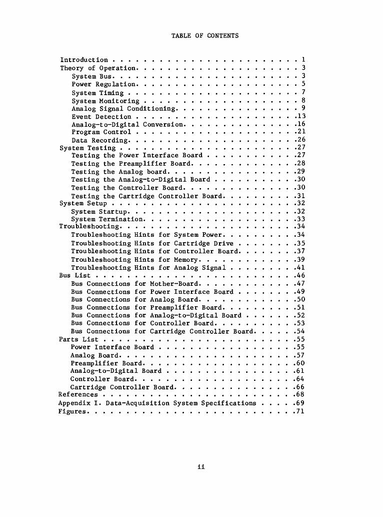
TABLE OF CONTENTS
Introduction ........................ 1Theory of Operation. .................... 3
System Bus. ....................... 3Power Regulation. .................... 5System Timing ...................... 7System Monitoring .................... 8Analog Signal Conditioning. ............... 9Event Detection .................... .13Analog-to-Digital Conversion. ............. .16Program Control .................... .21Data Recording. .................... .26
System Testing ...................... .27Testing the Power Interface Board ........... .27Testing the Preamplifier Board. ............ .28Testing the Analog board. ............... .29Testing the Analog-to-Digital Board .......... .30Testing the Controller Board. ............. .30Testing the Cartridge Controller Board. ........ .31
System Setup ....................... .32System Startup. .................... .32System Termination. .................. .33
Troubleshooting. ..................... .34Troubleshooting Hints for System Power. ........ .34Troubleshooting Hints for Cartridge Drive ....... .35Troubleshooting Hints for Controller Board. ...... .37Troubleshooting Hints for Memory. ........... .39Troubleshooting Hints for Analog Signal ........ .41
Bus List ......................... .46Bus Connections for Mother-Board. ........... .47Bus Connections for Power Interface Board ....... .49Bus Connections for Analog Board. ........... .50Bus Connections for Preamplifier Board. ........ .51Bus Connections for Analog-to-Digital Board ...... .52Bus Connections for Controller Board. ......... .53Bus Connections for Cartridge Controller Board. .... .54
Parts List ........................ .55Power Interface Board ................. .55Analog Board. ..................... .57Preamplifier Board. .................. .60Analog-to-Digital Board ................ .61Controller Board. ................... .64Cartridge Controller Board. .............. .66
References ........................ .68Appendix I. Data-Acquisition System Specifications . . . . .69Figures. ......................... .71
ii

ILLUSTRATIONS
Figure 1. Block diagram of the geophysicaldata-acquisition system. ........... .72
2. Aliasing of analog signals .......... .733. Block diagram of event detection circuitry . . .744. Block diagram of gain-ranging circuitry. . . . .755. Location of circuits boards on the
system bus .................. .766. User connections and controls. ........ .777. Component layout of the power interface
board. .................... .788. Component layout of the analog board ..... .799. Component layout of the preamplifier board . . .80
10. Component layout of the analog-to-digitalboard. .................... .81
11. Component layout of the controller board . . . .8212. Schematic of the power interface board .... .8313. Schematic of the event-detection circuits
on the analog board. ............. .8414. Schematic of the preamplifier board
and anti-aliasing filters on the analog board. .8515. Schematic of the analog-to-digital board
channel 1 and timing ............. .8616. Schematic of the analog-to-digital board
channels 2 and 3 ............... .8717. Schematic of the analog-to-digital board
channel 4. .................. .8818. Schematic of the controller board
adressing and input/output circuits. ..... .8919. Schematic of the controller board
memory circuits. ............... .90
iii

INTRODUCTION
The design goal for the U.S. Geological Survey (USGS) Ocean Bottom Seismometer Program has been to develop a geophysical data-acquisition system (GDAS) that can meet the requirements of wide dynamic range, programmable modes of operation, large data storage capacity, small size, and low power. The instrument's intended use involved four applications: an ocean-bottom instrument package for long-term seismic studies and short-term seismic refraction studies, a four-component surface buoy with FM telemetry and digital recording for use in refraction experiments, two- and four-component land systems for use in onshore seismic studies, and a real-time, high-resolution, data-acquisition system for geophysical studies. Other specifications required the ability to acquire data for as long as three months with up to four channels of analog input, a time channel with an accuracy of 100 milliseconds over a two month period, 120 dB of dynamic range, anti-aliasing filters, event-detection capability, and timed-window capability.
The basic design for this system was developed at the U.S. Geological Survey (Ambuter and Davis, 1981) using a modular approach to maximize its usefulness. The GDAS started out as a discrete component system, using a reel-to-reel recorder for data storage. This system did show some success in data acquisition, but difficulties with the tape formatting and the playback software resulted in little useful data recovery. In addition, system flexibility, low system noise, and wide dynamic range were not achieved. In 1982, the GDAS was redesigned as a microprocessor-based system (Ambuter and Godley, 1983) using a bus structure similar to the S-100 IEEE standard (Elmquist et al., 1979) and a cartridge tape drive for data storage. A block diagram of this system is shown in Figure 1. The modular approach was maintained by designing boards for specific functions, including power control, analog conditioning, analog-to-digital conversion, system control, and data storage.
The GDAS detects analog signals from geophones and hydrophones, and records these signals as digital words on magnetic tape. There are four channels of data acquisition in the GDAS: the first three are designed to receive signals from a geophone and the fourth channel is designed for a hydrophone input. The low-level signals from the sensors are amplified to increase the signal level high enough for the analog-to-digital converter to digitize it. The signals are then filtered to remove the unwanted high frequencies; any DC offset generated by the amplifier and filter circuits is also removed. After filtering, one channel can be connected to an event-detector circuit to permit the system to record data when a seismic signal is detected. Otherwise, the system will operate on a timed-window mode where the system will record data at a specified time only. The analog signals for each channel enter a gain- ranging amplifier that increases the dynamic range of the analog circuitry, allowing the system to record signals as small as a microvolt and as large as 30 millivolts. The resulting gain of this circuit is saved and recorded as a 4-bit gain code. The signals enter a sample-and- hold circuit, which holds the signal long enough for the analog-to- digital converter to digitize it, and, finally, are sent to an analog- to-digital (A-D) converter where the analog signal is converted to a 16- bit digital word. The lower 12 bits of the 16-bit word represent the result of the A-D conversion, and the upper 4 bits represent the gain code from the gain-ranging amplifier. The data word is entered into the

memory buffer and is recorded on tape after the memory buffer is filled. Two modes of operation determine how data are placed into the memory
buffer. In the timed-window mode, no data are placed into memory until the designated start time of each window has been reached. The memory buffer is then filled with data until the buffer is full; the data are then written to tape. In the event-detection mode, the memory buffer is continuously filled with data in a circular fashion and, when filled, starts over at the beginning. This continues until the event-detector indicates that a seismic signal has been detected. When this happens, the system checks to see how much data are desired beyond the event (a value that is programmed into the GDAS at start up). The memory buffer will continue to fill with data until that preset value is reached and, will then write the data to tape.
The GDAS has proven to be a useful tool when incorporated into the Ocean Bottom Seismometers (OBS's) in short-term refraction studies. The dynamic range of the data is only 90 dB, but this has not proven to be much of a handicap in these studies. FM telemetry was never implemented, and using this system as a high-resolution, seismic-reflection system is not possible because the GDAS cannot transfer the data to tape fast enough for most applications. The specifications of the current system are shown in Appendix I.

1. THEORY OF OPERATION
The GDAS is designed specifically for the acquisition of geophysical data in remote environments. It provides the circuitry for power distribution and communications between boards (the system bus), power regulation, system timing, system monitoring, analog signal conditioning, event detection, analog-to-digital conversion, program control, and data recording. This section describes the function of that circuitry and traces the various signals through the electronic components used. These descriptions make reference to various part numbers and connector pin numbers in the schematics listed in Figures 12 through 16 to aid in understanding the various operations.
1.1 SYSTEM BUS
The data-acquisition electronic package consists of six boards connected to a bus that is based on the S-100 IEEE standard (Elmquist et al., 1979). This bus consists of 100 parallel lines etched on a printed circuit board containing seven, 100-pin connectors tied to the parallel lines. These lines provide the means by which the boards communicate with each other and are divided into five groups: 1) power and ground lines, 2) address lines, 3) data lines, 4) control signal lines, and 5) undefined or spare lines. Some of the spare lines of this bus have been assigned to meet the unique requirements of the GDAS, and a complete listing of their function for each board is given in section 5. The bus used in the GDAS has several modifications to permit communication with devices not on the system bus, such as the cartridge drive, the terminal used to program the system, and a liquid crystal display. These modifications also provide a means to transfer analog signals between boards on the bus. This requires that the boards occupy specific slots on the bus. As shown in section 5.1, slot number 1 uses pins 4 through 17 to communicate with external devices. The power interface board contains the circuitry to control these devices, hence occupies slot number 1. Board numbers 2, 3, 4, and 5 are designed to pass analog signals on pins 5 through 17 and pins 55 through 67 of the bus. To properly connect the various analog signal paths together, the analog board must occupy the number 2 slot; the preamplifier board, the number 3 slot; and the analog-to-digital board, number 4 slot. The number 5 slot is left open for expansion. Slots 6 and 7 are occupied by the controller board and the cartridge controller board. Although either board can occupy either slot, external connections to the cartridge controller board are far simpler if it occupies the number 7 slot. Figure 5 illustrates the physical locations of these board on the system bus.
The power and ground lines transmit the voltages needed to power each board on the bus. As shown in section 5.1, a regulated +5 volts is available on pins 1 and 51 of the bus, and a regulated -5 volts is available on pins 21 and 54 of the bus. Regulated power is supplied on these lines to simplify design of each board (i.e., there is no need for voltage regulators on each board) and to conserve power, since one regulator consumes less power than many regulators. The system ground is the 0 volt reference for the system and is available on pins 20, 50, 67, 70, and 100 of the bus. These pins are connected together on the power interface board and are common for both analog and digital signals. An unregulated +12 volts is available on pin 2 of the bus, and an unregulated -12 volts is available on pin 52 of the bus. These voltages,

which are provided for expansion purposes, are not currently used in the system.
Address lines provide a means for the controller board to communicate with other boards on the system bus. This board is responsible for all of the system communications, and each board in the GDAS is designed to recognize a specific code word generated by the controller board when it needs to communicate. This code word is sent through the bus on the eight address lines, labeled AO through A7, which are connected to all of the boards on the bus. Each board compares the word sent by the controller board with its own code word to determine if it is the one being addressed. The address word is constructed of the eight lines, each having one of two logic states: either a high (+5 volts) or a low (0 volts). The address word is commonly described using binary notation where a value of 1 indicates a high, and a value of 0 indicates a low. The eight binary numbers are also combined to a single number using hexadecimal notation. Hexadecimal notation is based on 16 symbols (0 through 9 and A through F) and is constructed in powers of two using the binary number generated on the eight address lines. The hexadecimal value of these lines is as follows:
A7 A6 A5 A4 A3 A2 Al AO address lines80 40 20 10 8 4 2 1 hexadecimal value
The address for the analog-to-digital board, for example, demonstrates how the various logic states can be presented in both binary and hexadecimal notation. This board responds when the following logic states are present on the bus:
A7 A6 A5 A4 A3 A2 Al AO address lines000+5+5000 voltage level00011000 binary value0 0 010 8 0 0 0 hexadecimal value
The hexadecimal number is obtained by adding all the values together. In this case, the hexadecimal number is 10+8 or 18. The addressing requirements for each system function will be discussed later in this section, and both binary and hexadecimal values will be given. The binary value will aide in following the digital signal path, and the hexadecimal value will aide in following any software used in this system.
The data lines on the bus provide a means for the controller board to transmit to or receive data from other boards on the bus. The information contained on the data lines is always coupled with a specific address on the address lines, as discussed above. The address selects the board for communication and the data represents the message sent or received. There are two sets of data lines used in this bus: the data- out (DO) lines that send data from the controller board to the board being addressed, and data-in (DI) lines that send data from the board being addressed to the controller board. There are eight lines for each of these functions, and they operate in the same manner as described for the address lines.
The control lines allow the controller board to control data flow on the bus. Four of these lines are used to indicate whether data are to be received or sent. These lines are sIN (pin 46 of the bus) and pDBIN (pin 78 of the bus), which indicate to the board being addressed that data are

to be sent to the controller board, and sOUT (pin 45 of the bus) and PWR* (pin 77 of the bus), which indicate to the board being addressed that data are to be received from the controller board. VIO (bus pin 4) is an interrupt flag, sent from the analog-to-digital board to the controller board, that indicates data are available. CLOCK (bus pin 49) is the system's reference clock, and provides the time base for all boards used in the system.
The undefined lines of the bus are used by the system to pass analog signals among adjacent boards. Section 5.1 illustrates the layout of these lines on the bus, and they will be described in more detail later in this section.
1.2 POWER REGULATION
The power regulation circuitry in the GDAS is located on the power interface board. The part numbers and pin numbers used in this discussion are illustrated in Figure 12.
Using the GDAS for remote geophysical applications requires battery- supplied power for operation. Various components within the system require direct current (DC) voltages of +5 volts, -5 volts, +12 volts, and -12 volts. The system, however, is powered with a battery that provides only +12 volts and -12 volts. This was done for two reasons. First, it simplified the requirements for the battery (i.e., two automobile batteries could be used in land applications). Second, the electronic components that make up the system require +5 volts and -5 volts regulated to within .25 volts for proper operation. The battery voltage drops with usage and cannot, therefore, provide the necessary regulation. Instead, voltage regulators (electronic components that sense and hold the voltage to a defined level) are used to provide proper regulation to +5 volts and -5 volts. Battery voltages enter the power interface board on connector PI using specific pins. Pins 1 and 4 have been removed so that the connector can be keyed to prevent an accidental reversing of the plug. Pins 6 and 8 supply the ground for the entire system, and are tied together to exit the board on pins 20, 50, 67, 70, and 100 of the bus connector. Again, this common ground is for both analog and digital signals. The +12 volts from the battery enter the board on pin 2 of connector PI and first pass through a 3-amp microfuse (F2). This fuse provides protection for the battery in the event that a component failure should overload the battery capacity. The +12 volts exits the power interface board at bus pin 2 to provide this voltage to the other boards on the bus. The +12 volts also supplies power to the +5 volt regulator (Q2), which provides the regulated +5 volts to the oscillator (Yl) and to other boards on the bus via pins 1 and 51 of the bus connector. A battery backup circuit is also connected to the +12- volt input of this regulator. The circuit consists of two, 9-volt transistor batteries that maintain power to the system in the event of a power failure. This option is enabled by SW2. In addition, the backup provides for situations where the program is loaded while being powered by a bench supply before being transferred over to a field power source. The batteries provide this backup power for at least 1 hour during such an operation. The regulated +5 volts pass through a 2-amp microfuse (F5) before leaving the power interface board in order to protect the regulator from overload. The -12 volts enter the power interface board on pin 3 of connector PI and pass through a 2-amp microfuse (Fl). This voltage exits the board at bus pin 52, supplying this voltage to other

boards on the bus. The -12 volts also supplies power to the -5 volt regulator (Q3), which provides regulated -5 volts to pins 21 and 54 of the bus.
The cartridge controller board and drive in the GDAS require +5 volts, +12 volts, and -12 volts. The +12 volts and the -12 volts are not regulated because this voltage only powers the motor in the cartridge drive, and it can operate on voltages ranging from 10.5 to 14.5 volts. The +12 volts enter the board on pin 7 of connector PI and are passed through a 2-amp microfuse (F3) to protect the battery from overload. The -12 volts enter the board on pin 3 of connector PI and pass through a 2- amp microfuse (Fl) that protects the battery. The voltage inputs are separate from the ones described earlier, providing the option of using a separate battery to power the cartridge drive. The +12 volts also supplies power to the 10-amp adjustable regulator (Ql) that is set to a value of +5.1 volts under load (while the cartridge drive is recording data) with resistor R3. This regulated +5 volts powers the logic circuits of the cartridge controller board and drive, and is separated from the +5 volts described earlier to prevent any failures in the cartridge drive from affecting the operation of the rest of the system.
The GDAS is designed as a battery-powered system that operates for long periods of time in a remote environment, and under such conditions, the battery must last as long as possible to maximize the length of time the GDAS can record data. Since the cartridge drive requires 2.5 amps of power and is only needed when writing data to tape, the voltages are switched on and off through two relays located on the power interface board. The +12 volts, entering the board on pin 7 of connector PI, are connected to pins 3 and 4 of relay K2. The -12 volts, entering the board on pin 5, are connected to pins 9 and 10 of relay K2. When the relay is engaged, +12 volts exit the board on pins 7 and 8 of the bus, and the -12 volts exit on pins 9 and 10 of the bus. These lines, in turn, are connected via an external plug to the drive. The output of the +5 volt regulator (Ql) enters relay Kl. The outputs from this relay exit the board on pins 4, 5, and 6 of the bus, and enter the cartridge controller board and the cartridge drive through an external connector that is wired directly to the bus. Control signals, used to activate the relay, are usually noisy and often prevent the relay from making solid contact. A diode is used to prevent current reversals which might cause the relay to reopen after closing, and a capacitor is used to filter the noise out of the control signal. Together these components "debounce" the action of the relay. Diode CR10 and capacitor C8 are used to debounce the action of relay K2, and diode CR12 and capacitor C9 are used to debounce the action of the relay Kl. These relays are activated when the controller board sends the proper data word to the power interface board via the system bus. The controller board must do two things in order to switch the relays on or off: address the power interface board and send the data (or command) word. The controller board addresses the power interface board at address OFF H (hexadecimal) or:
A7 A6 A5 A4 A3 A2 Al AO bus address lines11111111 binary value
83 82 29 30 31 81 80 79 bus pin #s connected
These address lines are fed into the inputs of the 8-input, NAND gate U2. This NAND gate is a switch that goes low (0 volts) when all eight of its inputs are high (+5 volts), and high if any of the inputs are low. This,

along with control signals PWR* (pin 77 of the bus) and sOUT (pin 45 of the bus), enable data to be directed to the power interface board.
Two data words control the +12 volts and -12 volts to the cartridge drive through relay K2 and are sent by the controller board, via the data-out lines of the bus. The word to enable the +12 and -12 volts is 83 H or:
D07 D06 DOS D04 D03 D02 D01 DOO bus data-out lines10000011 binary value
90 35 36 bus pin #s connected
The data word to disable the +12 and -12 volts is 03 H or:
D07 D06 DOS D04 D03 D02 D01 DOO bus data-out lines00000011 binary value
90 35 36 bus pin #s connected
Data lines DOO, D01, and D07 are connected to the inputs of the 8-bit, addressable latch U3, which selects one of eight outputs depending on the logic states of the three inputs. DOO and D01 determine which of the eight outputs is to be changed, and D07 determines the logic level of that output. In this case, output Q3 (pin 7 of U3) will switch on or off the +12 volts and -12 volts to the cartridge drive through transistor Q5.
Two data words can be sent by the controller board to control the +5 volts to the cartridge controller card and the cartridge drive. The data word that turns the +5 volts power on is 80 H or:
D07 D06 DOS D04 D03 D02 D01 DOO bus data-out lines10000000 binary value
90 35 36 bus pin #s connected
The data word that turns the +5 volts power off is 00 H or:
D07 D06 DOS D04 D03 D02 D01 DOO bus data-out lines00000000 binary value
90 35 36 bus pin #s connected
Data lines are connected to the inputs of U3 as described above. In this case, output QO (pin 4 of U3) will turn on or off the +5 volts to the cartridge controller and drive through transistor Q4. To prevent controller problems, the +5 volts should be turned on first, then the +12 and -12 volts. When power is turned off, the +12 volts and -12 volts is removed first, then the +5 volts. This prevents any stray tape movement during power up and power down.
1.3 SYSTEM TIMING
Timing is extremely important in geophysical data-acquisition systems, because the time-of-day is the only identifier for the data being acquired. To illustrate the timing requirements, consider an array of systems deployed in an area of earthquake activity. The recorded time- of-day determines the exact moment each system detects an earthquake, and the accuracy of this time, especially between systems, directly affects the accuracy in determining the location of the earthquake (epicenter). The earthquake can be viewed as a sinusoidal wave with a frequency of 10 hertz, for example, that travels through a medium (the upper crust of the

earth) at a velocity of 5 kilometers/second. Determining the epicenter location within a ten percent accuracy translates into measuring a 500- meter wavelength to a precision of 50 meters. Because the timing required to resolve this 50 meters is 10 milliseconds, all systems in the array must maintain time accuracy to within 10 milliseconds of each other in order to maintain the 50-meter accuracy.
The time-of-day in the GDAS is maintained by a clock located on the controller board. The accuracy of this clock is determined by the oscillator that provides the counting pulses to it. The frequency required to operate the GDAS, 2,097,152 hertz, is determined by the components that make up the system. At this frequency, the accuracy of the oscillator must be within .03 hertz for the time error to be no more than 10 milliseconds at the end of a 30-day experiment. This could be achieved by using an oven-controlled oscillator, which typically has an accuracy within 0.01 hertz. The drawback, however, in using this type of oscillator is the large power consumption needed for operation. Low power versions require 250 milliamperes of power, which is three times the power consumption of the remainder of the system. The GDAS, instead, uses a temperature-compensated oscillator that requires only 3 milliamperes of power. The accuracy of this oscillator is 0.3 hertz, which translates into a time accuracy of 100 milliseconds for a thirty day experiment. The controller board, however, provides a means of measuring the clock drift that corrects the time to within 10 milliseconds. The clock drift measurement will be discussed in greater detail later in this section. The oscillator (Yl) is located on the power interface board and provides the 2,097,152 hertz clock pulses to all boards on the bus via bus pin 49 (see Figure 12).
1.4 SYSTEM MONITORING
The GDAS provides a means of monitoring the operation of the system performance by displaying a number on a liquid crystal display (LCD) mounted outside the system bus. The monitor typically displays the number of data events that have been recorded on tape. This information is useful in determining that the system is operating and provides a means of determining tape usage. Obviously, the display is only useful in experiments where the system can be observed. In ocean-bottom applications, where monitoring the system is impossible, the LCD counter is not used. The power interface board contains the logic necessary to drive an LCD counter via commands sent through the bus from the controller board. The following is a description of the commands that control the LCD counter and the circuitry involved (see Figure 12).
The power interface board is addressed at OFF H (hexadecimal), as described in section 1.2. Four data words can be sent by the controller board to control the action of the LCD counter. The data word to send a low (0 volts) to the LCD clock is 01 H or:
D07 D06 D05 D04 D03 D02 D01 DOO bus data-out lines00000001 binary value
90 35 36 bus pin #s connected
The data word that sends a high (+5 volts) to the LCD clock is 81 H or:
D07 D06 DOS D04 DOS D02 D01 DOO bus data-out lines10000001 binary value
90 35 36 bus pin #s connected
The data word that sends a low to the LCD reset is 02 H or:
D07 D06 DOS D04 D03 D02 D01 DOO bus data-out lines00000010 binary value90 35 36 bus pins #s connected
The data word that sends a high to the LCD reset is 82 H or:
D07 D06 D05 D04 D03 D02 DOl DOO bus data-out lines10000010 binary value
90 35 36 bus pin #s connected
Data lines are connected to the inputs of U3, as described in section 1.2. In this case, output Ql (pin 5 of U3) enters the LCD counter clock via pin 13 of the bus, and output Q2 (pin 6 of U3) enters the LCD counter reset via pin 14 of the bus. The LCD counter requires a falling edge (the drop from +5 to 0 volts) to increment, and a rising edge (the increase from 0 to +5 volts) to reset. In order to increment the counter, it is necessary to first set the clock high (+5 volts) and then set it low (0 volts). In order to reset the counter, it is necessary to first set the reset low and then set it high.
1.5 ANALOG SIGNAL CONDITIONING
The analog signal conditioning circuitry provides four functions: the amplification of the analog signals from the sensors, filtering of these signals, removal of DC offset, and waterbreak signal conditioning. This circuitry is contained on the preamplifier board and the analog board.
The analog signals from the sensors enter the GDAS on four connectors located on the preamplifier board (see Figure 14), and range in magnitude from less than one microvolt to 30 millivolts. The smallest signal detectable by the analog-to-digital board is 250 microvolts (see section 1.7), so signals must be amplified to increase the levels to the 250- microvolt detection limit of the analog-to-digital board. The preamplifier board amplifies the signals from the geophones in channels 1, 2, and 3 and from a hydrophone in channel 4. The preamplifiers Ul to U4 are low noise, wide bandwidth, instrumentation amplifiers set up to run on +5 volts and -5 volts. These amplifiers operate in two modes, inverting and noninverting. In the inverting mode, the amplifier output will be the reverse of the input: positive signals will be negative, and negative signals will be positive. This mode has a low input-impedence that can be adjusted using resistors located on the amplifier's input. The noninverting mode does not reverse the signal and provides an extremely high input-impedence. The amplifier is inverting for channels 1, 2, and 3 for best response with the resistive loads of the geophones. The gain and damping are set with resistors on headers located directly above each amplifier (see Figure 9). The amplifier is noninverting for channel 4 in order to maximize the response for the capacitive load of a hydrophone input. The gain and damping are set the same way as in the

other channels. The pin layout for these headers are as follows:
pin pin
1 H ///// I- 14 feedback (Rl)2 H ///// H 13 inverting input (R2)3 +--///// H 12 damping4 H | | h 11 -5 volts capacitor5 H | | J- 10 +5 volts capacitor6 H ///// H 9 noninverting input (R3)7 tZI/Z/Z/IT*" 8 ^in range
The gain of each amplifier for channels 1, 2, and 3 can be calculated by dividing the value of the feedback resistor (Rl) by the value of the inverting input resistor (R2). The gain of the first three channels is set to ensure that the smallest signal levels from the geophones are increased to the 250-microvolt detection limit of the analog-to-digital board. The resistor values, used in this design, are Rl = 220,000 ohms and R2 = 825 ohms. The gain is, therefore, 266.6.
The voltage gain (VG) for the channel 4 amplifier is calculated using the equation:
VG = 1 + (R1/R2)
The hydrophone voltage output is approximately half that of the geophone voltage output, so the feedback resistor (Rl) and the inverting input resistor (R2) for this amplifier are set to increase the hydrophone preamplifier output to that of the geophone preamplifiers. In this case, Rl - 5,760 ohms and R2 = 124 ohms. The gain is 466.
A damping resistor is required to maximize the response of the geophones. The damping resistor value is determined using the equation:
2 -7 BT - BO + G /[4 fm(Rl + R2)10 ]
where BT is the total damping (for maximum flatness, BT equals 0.707), BO is the open circuit damping of the geophone, G is the transduction of the geophone (in volts/centimeter/second), f is the resonant frequency of the geophone (in hertz), m is the suspended mass of the geophone (in grams), Rl is the value of the damping resistor (in ohms), and R2 is the value of coil resistance of the geophone (in ohms). The value of each of these parameters depends on the specifications for the geophone used with the GDAS. The equation is solved for Rl to determine the damping resistor value. Once calculated, the resistor should be installed in the headers (R3 for channel 1, R8 for channel 2, and R13 for channel 3) as shown Figure 9. No damping is required for the hydrophone preamplifier (channel 4), but a 2 megaohm resistor (R18) is installed to provide a high input-impedance to the amplifier.
Digitizing an analog signal allows the data to be recorded more compactly than an analog recording does and with greater dynamic range, since a digitized signal can record a greater voltage range than is possible with analog recording. The drawback to digitizing the signals , however, is that some of the data are lost. At specific intervals of time, the magnitude of the analog signal is recorded as a digital word, and all data in between these intervals are ignored. If the magnitude is
10

not recorded often enough, a false image (or aliasing) results when the analog signal is reconstructed from the digital words. For example, the analog signal can be represented as a sinusoidal waveform (see Figure 2) containing a peak and a trough for each cycle. If the signal is not sampled at least twice per waveform, the reconstructed waveform will have a lower frequency. This false lower frequency signal will combine with the real lower frequency signals of the data, creating a false image in the reconstructed waveform. To eliminate this problem, all unwanted high frequency signals are filtered out of the analog data before digitizing using an anti-aliasing filter. This circuit filters out all signals with frequencies greater than one quarter of the frequency of the digitization rate, ensuring that the data will not be aliased.
The anti-aliasing filters are located on the analog board (Figure 12). After being amplified on the preamplifier board, the analog signals enter the analog board via connector J2. Connector J6 also provides a means for the analog signals to enter this board via the system bus, but is no longer used in this manner because the microvolt analog signals are unrecoverable in the electronic noise level present on this bus. The analog board contains four identical channels, each one having an anti- alias filter with cutoff frequencies determined by a resistor header. The filter circuitry is a lowpass, 8-pole Butterworth, active filter with 48dB/octave rolloff, composed of four, second-order active sections at unity gain. The Butterworth filter design was chosen because this design has the flattest response of any of the standard filter types. The cutoff frequency is set using header resistors CM1 thru CM4 (see Figure 8). The resistor value for the desired cutoff frequency can be calculated by using the equation
6 R = 4.961x10 /f
Where f = cutoff frequency in hertz and R = resistance in ohms. The cutoff frequency is determined by sample rate, which is the interval of time between digitization of the analog signals. The GDAS is capable of digitizing the signals at sampling rates of 1, 2,4, and 8 milliseconds, which corresponds to sampling frequencies of 1024, 512, 256, and 128 hertz. The cutoff frequencies are calculated by dividing the sampling frequency by four, ensuring that at least four samples are digitized for each cycle of the analog signal. The resistor values are then calculated using the equation given above. Standard resistor values are used in the headers, so the actual cutoff frequency is modified to accommodate the use of standard resistor values. This is done by first calculating for the actual resistor value, selecting the closest standard value, and recalculating the cutoff frequency using that standard value. The following values can be used for the various sampling rates available:
Sample Rate Cutoff Frequency Resistor Value8 milliseconds 30 hertz 165.0k ohms4 milliseconds 60 hertz 82.5k ohms2 milliseconds 120 hertz 41.2k ohms1 milliseconds 248 hertz 20.0k ohms
11
After filtering, the signals leave the analog board through connector J7. This connector is actually a series of jumpers which provide the option to select one of three pins for each channel. The pin designations are as follows:
CH1 CH2 CH3 CH4 GND
__I__ __I__ ___I__ ___I__ _l_ 246 8 10 12 14 16 18 20 22 24 26 pin #
135 7 9 11 13 15 17 19 21 23 25 pin #I I I I I I I I I I I I I
55 56 57 58 59 60 61 62 63 64 65 66 67 bus pin #
Pins 25 and 26 continue the ground line along the bus. In the four channel mode currently being used, pins 1 and 2 , 7 and 8, 13 and 14, and 18 and 19 are jumpered for signals leaving the board. These connections are also shown in Figure 14.
The amplifier and filter circuits in the GDAS generate a DC offset: a constant voltage that is added to the signal as it passes through each circuit. This offset, in effect, alters the zero-volt level of the analog signal above or below the zero-volt level of the system. This effect is magnified each time the signal is amplified and can reduce the ability of the analog-to-digital (A-D) converter to digitize the signal. For example, a 4 millivolt signal enters the analog-to-digital board with a DC offset of 1 millivolt added to it. If the gain-ranging amplifier amplified the this signal by a factor of 1024, the total signal level would be 5.12 volts. The A-D converter in the GDAS, which digitizes signals between -5 volts and +5 volts, could not digitize this signal and data would lost. With no DC offset, the resulting voltage would be 4.09 volts, which is well within operating range of the A-D converter. Buffer amplifiers located on the preamplifier board remove the DC offset to maximize the useful range of the signals digitized. The buffer amplifiers, setup as an inverting amplifier with unity gain, are the same for all four channels and use the quad-amplifier U5 (see Figure 12). By using the inverting mode, the geophones signals are inverted back to their original form, and the input-impedance becomes the value of the resistor on the input to each amplifier. Note that the hydrophone (channel 4) signals, however, are now inverted. The buffer amplifiers are used essentially as large resistors, forming a RC highpass filter; the capacitors are located on the output of each anti-aliasing filter. The cutoff frequency can be calculated using the following equation:
f = 1,000,000/2RC
where f is equal to the cutoff frequency, R is the resistance (150,000) in ohms, and C is the capacitance (2.2) in microfarads. These values were chosen so that each filter will block out any signal that is less than 3 hertz, including any DC offset.
The analog board also contains the circuitry for a waterbreak amplifier. This is a specialized circuit designed for applications where rectified, high-frequency data from a hydrophone are desired. Data of this type are useful in determining the average voltage level of the background noise and the average voltage level of any seismic data signal. The hydrophone (channel 4) preamplifier output provides the input to the waterbreak amplifier. This amplifier consists of a 4-pole
12

lowpass filter that attenuates all signals above 1800 hertz, a full-wave rectifier that converts the signal into a positive DC voltage, and a 6- pole highpass filter that attenuates all signals below 600 hertz. The output of this amplifier can be (1) recorded as a separate data channel, (2) routed to the event-detection circuitry to trigger the system on direct arrivals, or (3) summed with the anti-aliasing filter output of channel 4. The output options are configured using jumpers on connectors J3 and J4 as shown in Figure 14.
1.6 EVENT DETECTION
Event detection is one of the modes of operation for the GDAS. In this mode, the system does not record data until a seismic event has been detected. A seismic event is any signal that is at some predefined level above the background noise. This mode of operation is commonly used to detect earthquakes and to record refraction data where the timing of the signals are unknown. The GDAS contains the circuitry to detect these events on the analog board with a hardware event-detector (see Figure 3) that uses a short-term averager (STA) versus a long-term averager (LTA). The LTA circuit averages the observed signal level over a 5-minute time period and represents the magnitude of the background noise present as the GDAS waits for an event. The STA circuit averages the signal level over a much shorter time period (50 - 500 milliseconds, set via software control during system start-up) and represents the magnitude of all noise (background and events) detected by the GDAS. An event occurrs when the magnitude of the STA exceeds the magnitude of the LTA.
The hardware event-detection circuitry runs independently of the controller board (see Figure 13), so when an event has been detected, the board must signal the controller board through the INT* line (pin 73 of the bus). The event signal is also sent to the output port buffer U20, where it can be monitored by the controller board if the interrupt flag cannot be used. The data signal used by the event-detector originates from the channel 4 input. This input can originate at the output of the anti-aliasing filter circuit, or the waterbreak amplifier circuit, or the summation of both outputs using a summing amplifier (part of U13). These inputs are configured using jumper pads J3 and J4 as shown in Figure 8. The data signal then enters an integrating amplifier (part of U13), which provides additional filtration to ensure that the signal is within the frequency range required by the event-detector. There are three capacitors that can be connected to the feedback loop of this amplifier through jumper pad J5, and the choice of capacitor depends on the sampling rate used in the analog-to-digital board of the system. The following diagram shows the connections for J5 using the various sampling rates.
Jumper for .5 ms sampling ._. | | C53
Jumper for 1 or 2 ms sampling . . | | C52
Jumper for 4 or 8 ms sampling . . | | C51
The capacitor provides an additional 6 dB of attenuation to the higher frequencies filtered by the anti-aliasing filter. The signal enters the digitally controlled attenuator U22, in the feedback loop of an amplifier (part of U13), which serves as a gain-ranging device to increase the
13

dynamic range of the event-detector from 40 dB to 76 dB. The digital control for the attenuator comprises 6 bits from two binary counters (U21 and U25). The counting is controlled by a comparator (part of U12) set at 50 millivolts. As the signal level goes up, the gain is lowered; as the signal level goes down, the gain is increased. This circuit allows the event-detector to resolve small signals from a high background noise level.
The signal then passes through two integrating amps (part of U19) that act as lowpass filters to attenuate all signals above 1.69 hertz at the rate of 3 dB/100 hertz. This further filters the data to the frequency range of interest for event-detection. At the output of this filter, the signal splits into two directions: one path goes to the long-term averager and the other, to the short-term averager. The long- term averager (LTA) circuit is made of three amplifiers (U15) and an analog switch (U16). One of the amplifiers is used as a feedback amp to aid in holding the long-term average when the circuit is disabled. This decreases the time required for the LTA to reestablish an average after the event has occurred. The first of the two remaining amplifiers is a full-wave rectifier that adds the negative voltage of the signal to the positive voltage. The result, a wavy positive DC signal, goes into the second amplifier, which acts as a averaging "storage" device. The RC filter network and the feedback to the full-wave rectifier average the signal level over a period of time, creating a slowly changing DC signal level. This time period is calculated by simply multiplying the feedback resistor value, in ohms, by the feedback capacitor value, in farads. In the GDAS, the feedback resistor is 165,000 ohms and the capacitance is 1,700 microfarads, resulting in a time constant of 4.7 minutes. The LTA is disabled during an event to prevent the event signal from biasing the long-term average signal. The switch control logic, a flip-flop in U24, responds when the controller board sends the proper command to the bus. The command is enable when the controller board addresses the analog board at 11 H (hexadecimal) or :
A7 A6 A5 A4 A3 A2 Al AO sIN sOUT bus address lines00010001 0 1 binary value
83 82 29 30 31 81 80 79 46 45 bus pin #s connected
This address is determined by the switch settings of SW-2 (see Figure 8). The base of the analog board is set at 10 H (hexadecimal) to accommodate the existing software, and requires that the switch settings be as follows:
1234 switch no. ./ . switch pos.
0001 binary value A7 A6 A5 A4 address lines
14

Address line A3 is used to set the compare circuit enabling control of the board. AO, sOUT, and sIN are used to control data input and output from the analog board. In addition to the address, the controller board sends the command word on the data-out lines of the bus. To disable the LTA circuit, the data-out lines contain 01 H (hexadecimal) or:
D07 D06 DOS D04 D03 D02 D01 DOO bus data-out lines00000001 binary value
90 40 39 38 89 88 35 36 bus pin #s connected
This command word enables the flip-flop output going to a comparator circuit (part of U12) which in turn disables the analog switch (U16). This action freezes the level of the LTA and stops the gain-ranging circuit. At this point the gain value of the digital attenuator is available to the controller board at the latch U20, which stores the gain word until it is read by the controller board. The address used by the controller board to read this data is 10 H or :
A7 A6 A5 A4 A3 A2 Al AO sIN sOUT bus address lines00010000 1 0 binary value
83 82 29 30 31 81 80 79 46 45 bus pin #s connected
The data are then presented to the bus on the data-in lines in the following format:
DIG bit 1 of gain wordDI1 bit 2 of gain wordDI2 bit 3 of gain wordDI3 bit 4 of gain wordDI4 bit 5 of gain wordDI5 bit 6 of gain wordDI6 no valueDI7 event flag
Note that the event flag appears on DI7. If the interrupt flag sent by the analog board to the controller board is not used, the controller can determine when an event has occurred by continuously reading this port. The DI7 line will have a binary value of one if an event has occurred, and a value of zero if no event has occurred. This line must be polled continuously or the controller board will miss the event.
The short-term averager (STA) is identical in structure to the LTA circuit, except that the STA has no disable function and its time constant is adjustable. The STA circuit is made up of two amplifiers (part of U19) and an analog switch (U18). The analog switch is used to select a capacitor on CM-8, which determines the signal storage time. Selecting C61 yields a 0.54-second time constant; selecting C62 yields a 0.25-second time constant; selecting C63 yields a 0.11-second time constant; and selecting C64 yields a 0.05-second time constant. The capacitor is selected by the data lines that go into the analog switch which are connected to the input port (U14), allowing the STA to be selected by the controller board. This parameter can also be manually entered by installing switch SW3 (see Figure 8), which is in parallel with U14. The output of the STA circuit is fed into a comparator circuit (part of U12) along with the output of the LTA circuit. This comparator circuit also has an analog switch (U17) that selects a resistor in order
15
to set the threshold level of the event-detector. The selection of the threshold resistor is accomplished in the same manner as the STA value, but uses analog switch U17. Selecting R102 yields a threshold of 6 dB; selecting R101 yields a threshold of 12 dB; selecting RlOO yields a threshold of 18 dB; and selecting R103 yields a threshold of 24 dB. In essence this resistor determines how much above the LTA signal level the STA signal level must be for the output to go high, indicating that an event has occurred.
To manually set the STA and threshold values to the event detector, install SW-3 and use the following switch settings:
Switch No. Value Selected
1 Threshold = 6 dB2 Threshold = 12 dB3 Threshold = 18 dB4 Threshold = 24 dB5 STA = 0.05 seconds6 STA =0.10 seconds7 STA =0.25 seconds8 STA = 0.50 seconds
Close one of the switches 1 to 4 to select a threshold, and close one of the switches 5 to 8 to select an STA value. The controller board selects the STA and threshold values by addressing the analog board at 10 H, as described earlier. These values are sent via the data-out lines in the following manner:
D07 D06 DOS D04 D03 D02 D01 DOO bus data-out lines
0001 Set THRESHOLD = 6dB0010 Set THRESHOLD = 12dB0100 Set THRESHOLD - 18dB1000 Set THRESHOLD = 24dB
0001 Set STA - 0.05 sec.0010 Set STA = 0.10 sec.0100 Set STA = 0.25 sec.1000 Set STA = 0.50 sec.
90 40 39 38 89 88 35 36 bus pin #s connected
The values are entered as one word, with the STA value filling the upper four data lines, and the threshold value filling the lower four data lines. This word also automatically enables the LTA circuit, allowing the event-detector to continue to operate. If more events are to be recorded, this data word must be sent after each event.
1.7 ANALOG-TO-DIGITAL CONVERSION
Converting an analog signal to a digital word allows the system to record data over a greater dynamic range Typical analog tape drives are capable of recording signals with a dynamic range of 48 dB. This means that if the maximum recorded signal is 10 volts, the smallest signal level that can be recorded is 39.1 millivolts. Digitizing the same 10 volts to a 20-bit number, as is done in the GDAS, produces a dynamic
16

range of 132 dB and the system can record a signal level as small as 8.3 microvolts. In remote operations where an unattended system must operate in environments of unknown background and data-signal levels, digitizingthe analog signals is a significant advantage over analog recording.
The GDAS analog-to-digital (A-D) circuitry is located on the analog-to-digital board. This board consists of four identical channels of A-D conversion with the logic necessary to generate these conversions. Each channel contains a 10-bit floating-point amplifier, a sample-and-hold circuit, a 12-bit A-D converter, and output steering logic. The circuitry is shown in Figures 15, 16, and 17. Since all four channels are identical, the following discussion will refer to the channel 1 circuitry shown on figure 15. The first numeral in each 1C label is an indication of channel. For example, 1C U101 indicates channel 1; U401, channel 4.
Analog signals enter the board from two different locations. One entry point is through connector J3 (see Figure 10) in which the channel 1 analog signal enters on pin 1, channel 2 on pin 2, channel 3 on pin 3, channel 4 on pin 4, and the signal ground on pin 5. The second entry point is from the bus using connector Jl. This is actually a series of jumpers that provide the option of selecting any three pins for each channel. The pin designations are as follows:
CH1 CH2 CH3 CH4 GND I I I I I
246 8 10 12 14 16 18 20 22 24 26 pin #
135 7 9 11 13 15 17 19 21 23 25 pin #III III III III I567 8 9 10 11 12 13 14 15 16 17 bus pin #
This configuration allows more than one A-D board to be used on the bus at one time, expanding the system to accommodate up to twelve channels. Pins 25 and 26 of the connector simply continue the ground line along the bus. In the four channel mode currently being used, pins 3 and 4, 9 and 10, 15 and 16, 20 and 21, and 25 and 26 are jumpered on the connector. This was done to correlate the inputs wired into the preamplifier board. Additional channels must be jumpered if more than one A-D board is used to pass data signals on through the bus, since the bus analog signal lines are not continuous.
The analog signal enters a gain-ranging amplifier, which extends the dynamic range of the system by providing an additional 10 bits to the digital word recorded for each sample. This corresponds to 60 dB of dynamic range that is added to the 72 dB of dynamic range provided by the 12-bit A-D converter. This circuit, developed in 1978 (Ambuter, 1979), consists of a programmable gain amplifier and a compare logic (see Figure 4) to maintain the signal level within defined limits. The compare logic automatically alters the gain of the circuit by changing the binary value loaded into the digital-to-analog converter in response to changes of the signal level. Although, the gain of the amplifier is set using 10 bits, the GDAS records a 4-bit code of the gain to conserve the amount of memory required to store each sample.
The 12-bit multiplying digital-to-analog (D-A) converter U106 is used as an attenuator to control the gain of amplifier U104 (see Figure 15). The D-A is a device containing 12-bits of binary input used to connect twelve resistors into the signal path. The binary input determines which
17
of the resistors is connected and sets the gain of amplifier U104. Only ten of the 12-bits of binary input are used to limit the maximum gain at 1024, and the minimum gain at 2. The D-A will decrement by a factor of two in response to an increase in signal level until a minimum gain of 2 is reached. The output of the amplifier is connected to the comparator 17111, which consists of four circuits that compares the signal level with a reference voltage connected to each circuit. The four outputs indicate whether the signal level exceeds the reference voltage level at each input. One output (pin 13 of Ulll) is referenced at +2.2 volts and indicates a high (+5 volts) if the signal level exceeds +2.2 volts. The second output (pin 12 of Ulll) is referenced at -2.2 volts and indicates a high if the signal level is less (more negative) than -2.2 volts. The third output (pin 10 of Ulll) is referenced to +0.1 volts and indicates a high if the signal level exceeds +0.1 volts. The fourth output (pin 11 of Ulll) is referenced to -0.1 volts and indicates a high if the signal is less than -0.1 volts. Together, these four outputs determine the binary value that sets the gain of the amplifier. The first and second outputs are connected to an AND gate on U109, and the output (pin 11) of this gate indicates a low (0 volts) if the signal is not between +2.2 volts and -2.2 volts. The third and fourth outputs of the comparator are connected to a NAND gate on U110, and the output (pin 6) of this gate indicates a high if the signal is not between +0.1 volts and -0.1 volts. These two signals control the action of the 4-bit counter U108. The counter will increment (increase the gain) if the signal level is between +2.2 and -2.2 volts, and decrement (decrease the gain) if the signal is not within this range. The counter also stops counting (no gain changes) if the signal is between +0.1 and -0.1 volts, and continues counting (change the gain) if the signal is not within this range. The counter U108 is setup for decade counting to prevent the 4-bit output from exceeding a value of ten. The carry-out signal of this chip and the MAX output of U107 is used to inhibit counting after minimum or maximum count is achieved. The count will update every 7.63 microseconds providing enough time for the comparator to settle between gain changes. The counting rate originates from the 12-stage binary counter U22, which divides the system clock (pin 49 of the bus) to provide the desired rate (131,072 hertz). The 4-bit output of U108 is connected to the inputs of the BCD-to-decimal converter U107, which converts the output of the counter to one of ten steps that directs the D-A. Since the D-A is binary, each step is 6 dB; ten steps totals 60dB of dynamic range. Before the signal is digitized by the A-D converter, the gain-ranging amplifier is halted to prevent any gain changes that might occur while the A-D converter is digitizing the signal. The 4-bit gain word is then stored in the upper four bits of the 8-bit latch U103, which transfers this data to the bus along with the digital word generated by the A-D converter. Note that the 4-bit gain code (CODE) is a compressed value of the 10-bit binary value (GAIN) used to set the gain of the gain-ranging amplifier. The following equation illustrates the relationship between these two values:
CODE GAIN = 2
The gain-ranging amplifier operates in a dynamic mode, in which the amplifier automatically adjusts its gain, or in a manual mode, in which the gain of the amplifier is fixed. These options are determined by the
18

controller board and transmitted through the system bus. The address required to communicate with the analog-to-digital board is 18 H (hexadecimal) or:
A7 A6 A5 A4 A3 A2 Al AO sIN sOUT bus address lines00011000 0 1 binary value
83 82 29 30 31 81 80 79 46 45 bus pin #s connected
This address is determined by the switch settings of SW-1 (see Figure 10). The base address of the analog-to-digital board is set at 18 H to accommodate the existing software, and requires that the switch settings be as follows:
1234 switch no. ./ .__.__.__. switch pos.
1000 switch val. A4 A5 A6 A7 address line
Address line A3 is used to set the compare circuit, enabling control of the board. sOUT and sIN are used to control the data input and data output from the analog board. In addition to the address, the controller board sends the command word on the data-out lines of the bus. The command word consists of the value needed to set the sample rate, a 4-bit gain word, and a manual/dynamic gain flag bit. The possible combinations are as follows:
D070
1
90
D060
1
40
DOS0
to1
39
D040
1
38
D03
01
89
D02
10101
88
D01
00110
35
DOO
11000
36
bus data outManual gain =
Manual gain =Man/dyn flagMan/dyn flagSample rate =Sample rate =Sample rate =Sample rate -Sample rate -
lines 2
1024= manual= dynamic8 ms (1284 ms (2562 ms (5121 ms (1024.5 ms(2148
hertz)hertz)hertz)hertz)hertz)
bus pin #s connected
The upper four bits (D04 to D07) represent the 4-bit gain code used when the manual mode is selected, and is identical in structure with the gain code described above. The code is substituted for the 4-bit output of the binary counter U108. The D03 line is the flag which indicates whether dynamic or manual mode is to be used. In the manual mode, the gain of the gain-ranging amplifier is fixed at the gain value entered in the upper four bits. In the dynamic mode, the gain will automatically adjust in response to the signal level and uses the output of the binary counter to set the gain. The lower three bits (DOO to D02) of the command word consist of the code necessary to set the sampling rate of the A-D converter. The sample rate will be discussed later in this section, but is presented now to fully describe the command word.
The analog signal from the gain-ranging circuit enters the sample- and-hold circuit which holds the signal level long enough for the A-D converter to digitize it. This circuit consists of the analog switch U20
19

and a 0.033 microfarad 1% capacitor that stores the signal level. When the switch is opened (i.e., on hold), the capacitor maintains the voltage for the A-D converter. When the switch is closed, the output of the sample-and-hold is the same as the output of the gain-ranging amplifier. The output of the sample-and-hold circuit contains the follower amplifier U105. This amplifier maintains a high-impedence output to the storage capacitor, preventing any extra loading of the capacitor that would result in a decrease in the signal level being stored.
The signal from the sample-and-hold circuit enters the A-D converter U101, which converts the magnitude of the analog signal to a 12-bit digital word. This device is set for bipolar, complimentary operation. Conversion is initiated by the timing logic and at completion, the digital word is sent to the 8-bit latches U102 and U103. The A-D converter sends a "conversion complete" signal to the timing logic when the digitization is complete; this, in turn, sets the interrupt flag to indicate to the controller board that data are ready. The controller board then reads the data from each of the four channels via the data-in lines of the bus. There are a total of sixteen bits of data (twelve from the A-D converter and four from the gain-ranging amplifier) for each channel, and since the data lines can only hold eight bits at a time, each channel must be read twice. The first eight bits, called the low byte, contain the lower eight bits from the A-D conversion, and are transferred to the bus in the following format:
Low Byte
DIG bit 1 of data wordDI1 bit 2 of data wordDI2 bit 3 of data wordDI3 bit 4 of data wordDI4 bit 5 of data wordDI5 bit 6 of data wordDI6 bit 7 of data wordDI7 bit 8 of data word
The second eight bits, called the high byte, contain the upper four bits of the A-D conversion and the 4-bit gain code from the gain-ranging amplifier. The high byte is transferred to the bus in the following format:
High Byte
DIG bit 9 of data wordDI1 bit 10 of data wordDI2 bit 11 of data wordDI3 bit 12 of data wordDI4 bit 1 of gain codeDI5 bit 2 of gain codeDI6 bit 3 of gain codeDI7 bit 4 of gain code
20

The analog-to-digital board responds to eight different addresses in order to provide the controller board with the means of reading all of the data. The following addresses send data from each channel of the A-D to the bus:
A7 A6 A5 A4 A3 A2 Al AO sIN sOUT bus address lines
00011000 1 0 Low byte CH1 A-D00011001 1 0 High byte CH1 A-D0001101010 Low byte CH2 A-D00011011 1 0 High byte CH2 A-D0001110010 Low byte CH3 A-D00011101 1 0 High byte CH3 A-D0001111010 Low byte CH4 A-D00011111 1 0 High byte CH4 A-D
83 82 29 30 31 81 80 79 46 45 bus pin #s connected
The timing required by the A-D board is the same as the digitization rate (called the sampling rate) of the A-D converter. The rate code is derived by the controller board and sent over the bus to the A-D board, as described above, where the code is stored in latch U13. The programmable counter U15 divides the clock pulse from counter U22 by the code stored in latch U13 to produce the sample rate clock. This clock initiates the action of U17, which is used as a shift register to control all of the steps required for conversion of a sample. The clock rate for each step is set at 65,536 hertz (15.26 microseconds) which is derived from U22. The following steps are required to convert a sample:
1. The gain-ranging amplifier is stopped to freeze the gain.2. The sample/hold stores the signal level and the A-D
is started.3. Wait while A-D converts the sample.4. Set up to send data on "Convert Complete" signal.5. Disable the shift.
The "conversion complete" signal from the A-D converter sets the flip- flop U18, which sends a high (+5 volts) to the VIO interrupt (pin 4 of the bus). The interrupt is set low (0 volts) when the controller board reads the first data-byte from the analog-to-digital board.
1.8 PROGRAM CONTROL
The controller board is responsible for program control, storage of data in a circular memory buffer, communications to the user, time of day, and other input/output (I/O) functions. This board is based around the NSC-800 microprocessor, which was chosen because it is low power consumption and extensive instruction set, which reduces the amount of memory needed for the complex programs written to control the system. The board functions with a set of instructions (the software) encoded in the electrically programmable, read-only-memory (E-PROM) located on the controller board. Time-of-day is handled by a MM58167 real-time clock. An NSC-810A I/O controller handles 22 lines of bi-directional input and output, 128 bytes of random access memory (RAM), and two 16-bit timers. System memory consists of five 8 k-bytes of RAM. The circuits that
21

make up this board are illustrated in Figures 18 and 19.The microprocessor (CPU) used in this system is an NSC800 (U7), an
8-bit processor, that is set up in a standard configuration with the exception of the power-down mode and the interrupt structure. The gate arrangement U28, designed to wake the CPU on an interrupt, has not worked reliably, so the power-down mode is not used. Since there is no capability to generate a clock interrupt for window modes, the CPU cannot power-down as it must stay awake to poll the clock. The CPU can be reset using the momentary switch (SW1) located on the power interface board (see Figure 7). This switch will reinitialize the controller board without removing power to the system. The switch brings the reset line (pin 75 of the bus) to ground, and is also connected to an external reset line (pin 17 of the bus) to allow the CPU to be reset by an external device.
The CPU is capable of operating with 3 different modes of interrupts: mode-0, mode-1, and mode-2, but operates using the mode-0 interrupt structure when first powered up. Interrupts are signal lines that are connected directly to the CPU. When high, they cause the CPU to jump to a specific software routine located in the controller board's EPROM. When, for example, the interrupt VIO sent from the analog-to- digital board to the CPU is high, the CPU automatically jumps to the part of the software that supplies the instructions for reading data from the A-D board. Mode-0 interrupts provide eight possible interrupts into the CPU. The software instruction "Restart 0" in this mode directs the CPU to the start of the program at power up. All interrupts generated in the GDAS system use mode-1 operation, which enables four possible interrupts to the CPU. This mode was chosen because fewer circuits were required to support it. These interrupts are also sent to the port B of the I/O controller U8 and NAND gate U28 in an attempt to use the power-down mode of the CPU. The interrupts are enabled by setting the appropriate bits of port C on U8 to prevent the CPU from accidentally shutting down. INTR* (pin 25 of U7) is normally high, so no external setting of this interrupt is necessary. RSTA (pin 22 of U7) is enabled by setting PCO (pin 37 of U8) low, RSTB (pin 23 of U7) is enabled by setting PCS (pin 34 of U8) high, and RSTC (pin 24 of U7) is enabled by setting PC3 (pin 1 of U8) high. PCI (pin 38 of U8) can also be used to enable the power-down mode, which is currently not being used. The INTR* interrupt is used by the early termination button on the GDAS housing. This stops data acquisition and begins the program termination routines, which is done in software. RSTA interrupt is connected through U27 (a NOR gate) to the VIO interrupt (pin 4 of the bus) and is used by the A-D board to let the CPU know there are data available. RSTB interrupt is used by the output of timer 1 of U8. It is currently used as a error timer for the tape drive software routines. RSTC interrupt can be used by the incoming signal line of the RS232 port to wake the CPU if a terminal is connected. There is an additional input on the power-down mode gate which does not connect to the interrupts. This connection is from the timer 0 output and provides a means of waking up the CPU after a designated period of time. The nonmaskable interrupt (NMI) is connected to PC2 (pin 39 of U8) and can be used to change the system memory organization in system playback modes.
Communications to the RS232 terminal, the external satellite clock, and the internal RTC output are handled by the I/O controller U8, which has three ports available for I/O operations (labeled A, B, C). Port C is setup to initialize the interrupts as described earlier. Port B has
22

several functions, depending on which of the eight data lines are used. PBO (pin 29) is used to transmit data to the RS232 connector (XMIT) via pin 28 of the bus and pin 8 of connector P2. Amplifier U15 is used as a driver to supply enough power to interface properly with any standard terminal. FBI (pin 30) is used to enable U9 and Ull (data buffers to connector P3), which are currently not used. PB2 (pin 31) is used to reset the cartridge controller board via pin 65 of the bus. PB4 , PB5, and PB6 are used as inputs for the various interrupts as described earlier (PB4 for INTR*, PB5 for RSTA, and PB6 for the output of timer 0). PB7 (pin 36) receives the data from the RS232 connector (RCV) via pin 27 of the bus or pin 7 of connector P2 and through U15 which buffers the signals. Port A is setup as a general purpose parallel port. The design of the board indicates that all eight data lines go through data buffers U9 and Ull, which are connected to P3. This, however, was never implemented. Instead, only three of the data lines are used and these are connected directly to connector P3. PA1 (pin 22) is connected to pin 2 of connector P3, and goes high when the real-time clock (U10) indicates that a second has elapsed. PA2 (pin 23) goes high when U10 indicates that a minute has elapsed, and is connected to pin 4 of P3. These two lines are used to determine the drift of the real-time clock. The outputs are connected to an oscilloscope and compared with the second and minute pulse from a satellite clock. PAS (26) is an input by which the system can detect a pulse coming from the satellite clock that indicates a minute transition; it is connected to pin 6 of P3. This input is used by the system to synchronize the real-time clock with the satellite clock. There is also a provision at Ul for a relay that is activated when the data buffers were activated, but is not currently used.
The I/O controller has two timers available to the system. Timer 0 indicates a transition of one second. This timer uses the CPU clock (1,048,576 hertz) as a time base and, under software control, the clock is set up to divide by 64, producing a clock rate of 0.061 milliseconds. Preloading the clock with the hexadecimal value 3FFF H causes the counter to overflow once each second. Timer 1 has a time base of 256 hertz and is currently used as a time-out error trap for the cartridge drive.
The CPU uses all address locations from 3000 H to 3099 H to communicate with the I/O controller U8. A binary value of 0 in address line A15 enables the decoder U24, which enables one of the eight devices connected to its outputs as determined by the logic state of the three inputs. It is used in conjunction with decoder U23 to select all of the memory and I/O devices located on the controller board. Address line A15 is used to select U23 (a binary of 1) and U23 (a binary value of 0). Address lines A12, A13, and A14 provide the three inputs to both decoders and determine which of the sixteen devices connected to both decoders will be selected. In selecting the I/O controller U8, the address lines A12, A13, and A14 will contain binary values of 0, 1, and 1, respectively. Address lines AO-A11 are used to address a specific portion of the RAM or I/O that make up U8. The following is a list of the various locations in U8:
23
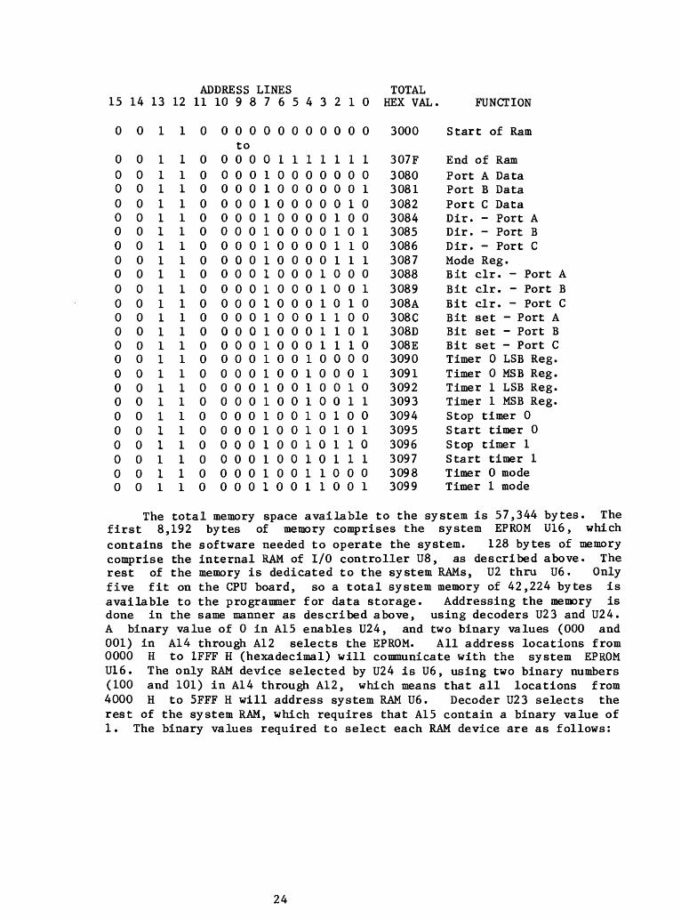
ADDRESS LINES TOTAL 15 14 13 12 11 10 9 8 7 6 5 4 3 2 1 0 HEX VAL. FUNCTION
3000 Start of Ram
307F End of Ram3080 Port A Data3081 Port B Data3082 Port C Data3084 Dir. - Port A3085 Dir. - Port B3086 Dir. - Port C3087 Mode Reg.3088 Bit dr. - Port A3089 Bit clr. - Port B308A Bit clr. - Port C308C Bit set - Port A308D Bit set - Port B308E Bit set - Port C3090 Timer 0 LSB Reg.3091 Timer 0 MSB Reg.3092 Timer 1 LSB Reg.3093 Timer 1 MSB Reg.3094 Stop timer 03095 Start timer 03096 Stop timer 13097 Start timer 13098 Timer 0 mode3099 Timer 1 mode
The total memory space available to the system is 57,344 bytes. The first 8,192 bytes of memory comprises the system EPROM U16, which contains the software needed to operate the system. 128 bytes of memory comprise the internal RAM of I/O controller U8, as described above. The rest of the memory is dedicated to the system RAMs, U2 thru U6. Only five fit on the CPU board, so a total system memory of 42,224 bytes is available to the programmer for data storage. Addressing the memory is done in the same manner as described above, using decoders U23 and U24. A binary value of 0 in A15 enables U24, and two binary values (000 and 001) in A14 through A12 selects the EPROM. All address locations from 0000 H to 1FFF H (hexadecimal) will communicate with the system EPROM U16. The only RAM device selected by U24 is U6, using two binary numbers (100 and 101) in A14 through A12, which means that all locations from 4000 H to 5FFF H will address system RAM U6. Decoder U23 selects the rest of the system RAM, which requires that A15 contain a binary value of 1. The binary values required to select each RAM device are as follows:
0
0 00000000000000000000000
0
0 00000000000000000000000
1
1 11111111111111111111111
1
1 11111111111111111111111
0
0 00000000000000000000000
0
0 00000000000000000000000
0 0to0 0 0 00 00 00 00 00 00 00 00 00 00 00 00 00 00 00 00 00 00 00 00 00 00 0
0
011111111111111111111111
0 0
0 00 00 00 00 00 00 00 00 00 00 00 00 00 00 00 00 00 00 00 00 00 00 0
0 0
0 00 00 00 00 00 00 00 10 10 10 10 10 11 01 01 01 01 01 01 01 01 11 1
0
00011110001110000111100
0 0
0 00 11 00 00 11 01 10 00 11 00 00 11 00 00 11 01 10 00 11 01 10 00 1
24

ADDRESS LINE RAM DEVICEA15
11111111
A1400001111
A1300110011
A12010101 o1
U5U5U4U4U3U3U2U2
All locations from 8000 H to FFFF H address the remaining system RAM. Hexadecimal values of 8000 H and 9FFFF H select U5; hexadecimal values of AOOO H and BFFF H select U4; hexadecimal values of COOO H and DFFF H select U3; and hexadecimal values of EOOO H and FFFF H select U2.
Real-time clock (RTC) U10 is used to keep track of time-of-day to within a millisecond. The time base originates with the CPU clock at a frequency of 1,048,576 hertz. This clock signal goes to the counter U14, dividing it to 32,768 hertz, and also passes through gates in U12 and U27 to allow for external start and reset of the RTC. This RTC uses a 5-bit address and a 8-bit data bus. All locations from 2000 H to 2017 H address the RTC. A value of 0 in A15 enables U24, and a binary value of 010 in A14 through A12 selects the RTC. Address line AO through All are used to address a specific portion of the clock. The following is a list of the various locations:
ADDRESS LINES TOTAL 15 14 13 12 11 10 9 8 7 6 5 4 3 2 1 0 HEX. VAL.
000000000000000000000000
000000000000000000000000
111111111111111111111111
000000000000000000000000
000000000000000000000000
0 00 00 00 00 00 00 00 00 00 00 00 00 00 00 00 00 00 00 00 00 00 00 00 0
0 00 00 00 00 00 00 00 00 00 00 00 00 00 00 00 00 00 00 00 00 00 00 00 0
0 00 00 00 00 00 00 00 00 00 00 00 00 00 00 00 00 00 00 00 00 00 00 00 0
0 00 00 00 00 00 00 00 00 10 10 10 10 10 10 10 11 01 01 01 01 01 01 01 0
0 00 00 10 11 01 01 11 10 00 00 10 11 01 01 11 10 00 00 10 11 01 01 11 1
010101010101010101010101
20002001200220032004200520062007200820092 00 A200B200C200D200E200F20102011201220132014201520162017
FUNCTION
MillisecondsTenths & hundredths sec.SecondsMinutesHoursDay of weekDayMonthLatch - millisecLatch - .xx secLatch - sec.Latch - min.Latch - hourLatch - day of wk.Latch - dayLatch - monthInterrupt statusInterrupt cmd.Time resetLatch resetTime statusStart reg.Standby interruptTest
25

The above latches are used for a programmed interrupt, which is not used in the GDAS. The clock is started by loading the current time during parameter entry. Synchronizing this time with a satellite clock is done using the procedure described earlier.
1.9 DATA RECORDING
Acquired data are stored on a cartridge tape recorder which has a data capacity of 17.5 megabytes. This system consists of a Digidata-6440 tape drive coupled with an Alloy IDXS-100 controller board. The cartridge controller accepts data in 8,192 byte blocks, writes the data to tape, and performs read-after-write verification. The cartridge write operation is transparent to the controller board allowing continuous digital data logging at 8192 bytes per second. Refer to the instruction manuals that accompanys these devices for any discussion of operations.
26

2. SYSTEM TESTING
The following section describes testing procedures for each circuit board of the GDAS that should be done prior to any usage of the system. The procedures in this section will refer to connector and other part numbers in describing locations of test points. These part numbers are referenced to the numbers printed on the circuit board being tested and examination of the circuit board will aid in locating these test points.
2.1 TESTING THE POWER INTERFACE BOARD
There are six tests that must be done to verify proper operation of the power interface board. The use of a voltmeter, 10-digit frequency counter, and a Rubidium (Rb) frequency standard are necessary to conduct these tests. The system must have all boards connected and an EPROM installed on the controller board.
Input Voltage - This checks the input voltages entering the power interface board to verify that the proper voltages are present before going on to other tests. The power source, whether it is a battery or other power supply, must provide two direct current (DC) voltages to the power interface board. These voltages must be a minimum of +12 volts and -12 volts to adequately power the system. These voltages must not exceed +15 volts or -15 volts, or damage will result to the tape drive. The power source must have an 8-pin, female, Molex connector to mate with the connector Jl (see Figure 7) on the power interface board. This connector must be terminated as follows:
|_1_l__2__l_3_l_4_r^5_r_6__r_7_|_8_| pin no. JBLNK j+12v |-12v |BLNK |-12v | GND |+12v I GND | voltage
The blank keys prevent accidental misallignment when connecting this plug to the power interface board. Insert the plug and measure the voltages on the lower pins of Jl. If the proper voltages are not present, check the power source for proper operation.
Bus Voltages - Voltages for the bus are located on bus pin 1 for the +5 volts, pin 54 for the -5 volts, pin 2 for the +12 volts, and pin 52 for the -12 volts. The +5 and -5 voltages should be within 0.15 volts of the given value. Both 12 volt values will read equal to the power source voltage levels as there is no 12-volt regulation. If the proper voltages are not present, refer to section 4.1 for troubleshooting.
Logic Supplies - In setting up the GDAS for operation, it is necessary to determine that the proper voltages are getting to each of the boards present in the system. Figures 8 to 11 show the location for measuring the voltages on each board. If the voltages are not present check the system bus connections.
Cartridge Drive Voltages - The measuring points for the cartridge drive voltages are at bus pins 4, 5, and 6 for the +5 volts, bus pins 7 and 8 for the +12 volts, and bus pins 9 and 10 for the -12 volts. These voltages are not sent to the cartridge drive until the two relays on the power interface board (see Figure 7) have been activated. There should be no voltage on any of the pins when the relays are open. If the proper
27

voltages are not present when the relays are activated, refer to section 4.2 for troubleshooting.
Oscillator - The system must be powered up for two hours to allow time for the oscillator to equilibrate. An 10-digit frequency counter, using a 10 MHz Rb standard as an external reference, is set up to measure the output of the oscillator. The probe of the counter should be connected to the test point of the oscillator as shown in Figure 7. Using the screw located on the top of the oscillator (under the screw cap), adjust the frequency to the value written on the oscillator. Be careful that no pressure is being exerted on the adjustment screw when the frequency count is being read. The adjustment should be made to within 0.1 Hz.
Reset Switch - The system should have a program E-PROM on the controller board and a terminal connected to the RS232 connector on the electronics rack (see Figure 6). Just push the reset button (see Figure 7) and see if the program will restart. The screen on the terminal should clear and display the system ram test. If this does not occur, refer to section 4.1 for troubleshooting.
2.2 TESTING THE PREAMPLIFIER BOARD
Testing the preamplifier board requires that you verify preamplifier operation and buffer amplifier operation. The use of an oscilloscope and a function generator are necessary for these tests.
Preamplifier - Apply a 10-millivolt, 20-Hertz sine wave to the input of each channel ( J2 is channel 1; J3 is channel 2; J4 is channel 3; and J5 is channel 4 - see Figure 9). Using the oscilloscope, measure the output of the preamplifier for each channel by connecting the scope probe on the output connector (Jl). Channel 1 is pin 5; channel 2 is pin 4; channel 3 is pin 3; and channel 4 is pin 2. The gain of the preamplifier for channels 1,2, and 3 is 266, so the output should be a sine wave with a magnitude of 2.66 volts. The gain on channel 4 is 466, so the output should be 4.66 volts.
Buffer Amplifier - First verify the operation of the analog board as described in section 2.3. Repeat the tests described above in the preamp section. To monitor the output of the buffer amps, connect the scope probe to the input connector (J3) on the A-D board (see Figure 10). Channel 1 is pin 1, channel 2 is pin 2, channel 3 is pin 3, and channel 4 is pin 4. The results should be the same, although the magnitude will drop slightly due to the filters.
Sensor Monitoring - In setting up the GDAS for deployment, it is possible to monitor the signals from the sensors to verify proper operation. Place the scope probe on the appropriate pins of J3 as described in testing the buffer amplifier, and connect the four sensor cables to the preamplifier board as illustrated in Figure 9. By tapping on the sensors, the waveforms shown on the oscilloscope should indicate the response of the sensors after being amplified, filtered, and the DC offset removed.
28

2.3 TESTING THE ANALOG BOARD
Testing the analog board requires that you verify filter response and operation of the event-detection circuits. The use of an oscilloscope, a signal generator, a +5 and -5 volt power supply, a logic signal generator, and an extender card are necessary for these tests.
Board Verification - Check the jumpers for proper connection on the analog output connector J7 as described in section 1.5. The filter cutoff frequency is set by installing resistor headers in CMl, CM2, CM3, and CM4 (see Figure 8). The following values can be used for the various sampling rates available:
Sample Rate Cutoff Frequency Resistor Value8 ms 30 Hz 165.0 k-ohms4 ms 60 Hz 82.5 k-ohms2 ms 120 Hz 41.2 k-ohms1 ms 248 Hz 20.0 k-ohms
Anti-Aliasing Filter - Apply a 20-hertz sine wave to the input connectors of each channel (located on the preamplifier board) as described in section 2.2. Attach a voltmeter or scope to the output of the filter (TP5 for channel 1; TP6 for channel 2; TP7 for channel 3; TP8 for channel 4 - see Figure 8). Then adjust the voltage level of the input so that the output equals 1 volt. Gradually increase the frequency of the sine wave until the output voltage equals 0.707 volts. This value should be 33 Hertz for the 156 k-ohm header; 66 Hertz for the 82.5 k-ohm header; 132 Hertz for the 41.2 k-ohm header; or 264 Hertz for the 20 k- ohm header. If the proper response is not observed check the capacitors used in the filter circuit.
Event Detector - Remove U14 and U26 (see Figure 8) and apply a 0.05- Hertz, 5-volt, signal to pin 1 of U26. Install jumpers on J3, J4, and J5 as follows (see Figure 8):
J3 J4 J5
Install a dip switch in SW-3 and set SW3-1 and SW3-5 in the closed position with the rest in the opened position. Check the settings on the addressing dip switch (SW-2) to ensure that all positions are closed except SW2-4, which is opened. Reset the system by pushing the reset button on the power interface board (see Figure 7). Apply a 20-Hertz sine wave to the input of channel 4, and adjust the amplitude to read 1 volt at TP16 (see Figure 8). Reset the system again. Wait 20 minutes and measure the voltage at TP15, which should be between 40 and 60 millivolts. Increase the input by 20db. The voltage at resistor R104 should go high to +5 volts, and then after a short delay drop to -5 volts.
29

2.4 TESTING THE ANALOG-TO-DIGITAL BOARD
This test requires a function generator, all boards installed in the system, an EPROM installed on the controller board, and some means of playing back the data recorded on tape. As an example, Ocean Bottom Seismometer operations use the OBS EPROM (Miller, 1986) and display the recorded data on the OBS playback system (Fredricks, et al, 1984). This test provides a means of evaluating the response of the analog-to-digital board under the experimental conditions determined by the operating software.
Board Verification - Check the jumpers for proper connection on the analog input connector Jl (see Figure 10) and the switch settings of the board addressing switch SW-1, as described in section 1.8.
Analog-to-Digital Conversion - Refer to the operating instructions for the particular EPROM installed in the GDAS to program the system for three, separate series of experiments. The first series is set to record several events with the inputs to all four channels shorted (a wire is connected from the signal input pin to ground) at the input connectors J2, J3, J4, and J5 located on the preamplifier board (see Figure 9). The second series is set to record several events with a 20-Hertz, 20- microvolt (peak-to-peak) signal on each channel. This should be done one channel at a time, using the input connectors located on the preamplifier board, with the other channels shorted. The third series is set to record several events with a 20-Hertz, 20-millivolts (peak-to-peak) signal on each channel. Again, test one channel at a time with the other channels shorted. Refer to the operating instructions for the playback system being used to determine the magnitude of the data recorded on tape. Compare the recorded signals with the signal entered into the system for each series. The first series should give a good indication of the system noise level. Series two and three should give a good indication of the minimum and maximum response of the A-D board. If no signal was recorded, refer to the troubleshooting guide in section 4.5.
2.5 TESTING THE CONTROLLER BOARD
Testing of this board is done while using the system software. At power-up, the software automatically checks the registers of the microprocessor. If there is a failure, a "bad processor" message will be displayed on the terminal. There is also a test for the system memory built into the software, which is also done at power up, that will display any errors found to the terminal.
Clock Drift - Connect the satellite clock to the CPU board as shown in Figure 6. Connect the satellite clock seconds output to channel 1 on the oscilloscope and connect the GDAS seconds output (as described in section 1.8) to channel 2 on the scope. Set the scope to trigger off of channel 1. The system program should be terminated at this point by pushing the early termination button (see Figure 6). The time of day from the GDAS will display once a second on the screen. Compare this time with the time shown on the satellite clock, and measure the clock drift on the scope to determine the number of milliseconds the time of the GDAS has drifted from the satellite clock time.
30

2.6 TESTING THE CARTRIDGE CONTROLLER BOARD
The cartridge controller is tested by the system software by automatically writing a test record and then reading it back. The pattern read from the tape is compared to the pattern in system memory. If this test fails, the message "BAD TAPE" will appear on the terminal.
31
3. SYSTEM SETUP
The following section describes the steps necessary to start up and terminate the data-acquisition system. When programming the system, refer to the software instruction manual that pertains to the EPROM being used in the controller board.
3.1 STARTUP
A. Check to be sure that all boards are located in the proper slots in the electronics rack, and that a ribbon connector is installed between the preamplifier board and the analog board (see Figure 5).
B. Remove the analog card, and check that resistor headers CMl, CM2, CM3, and CM4 are the proper ones for the sampling rate desired (see Figure 8). For an 8-ms rate, use a 162k-ohm header; for a 4-ms rate, use a 82k-ohm header; for a 2-ms rate, use a 4Ik-ohm header, and for a 1-ms rate, use a 20.5k-ohm header. Reinstall the analog card.
C. Verify that the proper E-PROM is installed in the controller card (see Figure 11).
D. Connect a power source (battery or power supply) to the 8-pin connector located on the power interface board and check the the voltages as described in section 2.1.
E. Attach the four sensor connectors to the preamp board (see Figure 9).
F. Check the logic supply voltages (+5 volts and -5 volts) and cartridge supplies as described in section 2.1.
G. Clean the tape head of the drive using a cotton swab and denatured alcohol. Install a tape into the drive.
H. Check the signal response for each of the sensors at the connector J3 of the A-D board as described in section 2.2.
I. Let the system sit powered-up for 2 hours, then adjust the oscillator as described in the section 2.1.
J. Connect the RS232 cable from a standard computer terminal to the RS232 connector on the GDAS electronics rack (see Figure 6). The terminal should be setup for space parity, 7 data bits, 1200 baud, 1 stop bit, and no handshake lines.
K. Connect the cable from the satellite clock (if used) to the connector located on the controller card (see Figure 6).
L. Reset the system by pushing the reset button on the power interface board (see Figure 6).
M. Enter program parameters as per software instructions. Note: Disconnect the satellite clock during the tape test.
32

3.2 TERMINATION
A. Connect the terminal and push the early terminator button (see Figure 6).
B. Terminate the system program as per software instructions.
C. Check clock drift and oscillator frequency as described in section 2.1 and 2.5.
D. Remove and label the tape.
E. Measure the logic and battery voltages, as described in section 2.1.
F. Remove the power.
33

4. TROUBLESHOOTING
4.1 TROUBLESHOOTING HINTS FOR THE SYSTEM POWER
/ SYSTEM DOESN'T START UP /
/ / no / / no / / / +12v-Pl pin 2 / / replace battery / / -12v-Pl pin 3 /
yes I yes
/ +5v-pin 1 bus / / -5v-pin 54 bus /
no no
/ / yes / / yes / / / bad fuse F2 / / replace fuse / / bad fuse Fl /
no no
/ bad fuse F5 /
I no
7 yes no / V / bad reg. Q3 /
7
I yes
/ 7 no / J I 7 I bad reg. Q2 / / see sec. 4.3 / / replace reg. /
yes
/ replace reg. /
yes
yes
34

4.2 TROUBLESHOOTING HINTS FOR THE CARTRIDGE DRIVE
/ CARTRIDGE DRIVE DOESN'T WORK /
/ / no / / no / / / +12V-P1 pin 7 / / replace battery / / -12v-Pl pin 5 /
I yes I yes
/ / yes / / yes / // bad fuse F3 / / replace fuse / / bad fuse F4 /
/ II II I
no1
I no
/ /no / working relay K2 / / / yes /
/ | / bad fuse F2 /____/ replace fuse/
yesno
I / / yes / /I / bad reg. Ql / / replace reg. /I / / / /
no
yes / / no / / _____/ coil voltage / / working relay Kl /
/ // toggling /
I I no
/ / yes / // bad Q4 or Q5 / / replace trans. /
/ II I
no
/ / no / / / Working U3 / / replace 1C /
I yes
yes
4.2 cont'd
35

/ I no / working Ul /____
II yes
/ / no / / / working U2 / / replace 1C /
yes
/ 7 / 7
/ replace relay / / check EPROM /
4.2 cont'd
/ / no / / no / / / good connector / / repair / / good connector / T to drive / / conn. / /to controller / ____________/ /______/ / board /
I / /I yesII
/ check drive / / see drive /
/ manual /
yes
/ check controller / / board / /see controller /
/ manual /
36
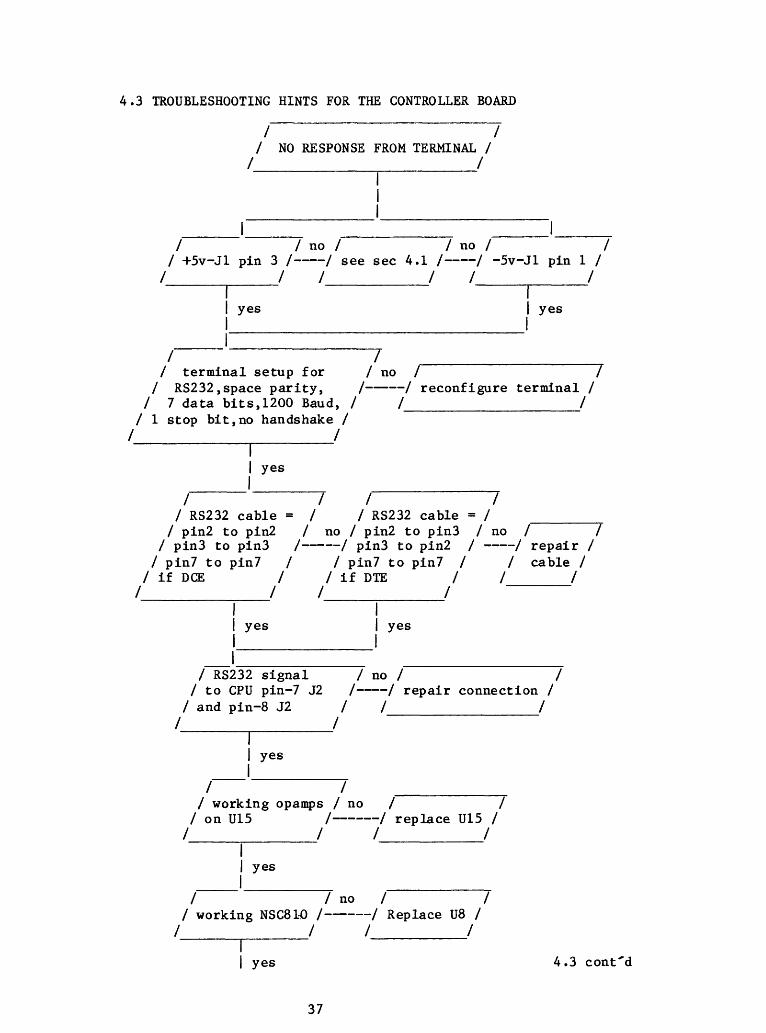
4.3 TROUBLESHOOTING HINTS FOR THE CONTROLLER BOARD
/ NO RESPONSE FROM TERMINAL /
/ j no i / no / / / +5v-Jl pin 3 / / see sec 4.1 / / -5v-Jl pin 1 /
II yes I yes I I
/ terminal setup for / no / 7 / RS232,space parity, / / reconfigure terminal /
/ 7 data bits, 1200 Baud, / /_________________/ / 1 stop bit,no handshake /
I yes
/ 7 / 7/ RS232 cable = / / RS232 cable = / _______
/ pin2 to pin2 / no / pin2 to pin3 / no / / / pin3 to pin3 / / pin3 to pin2 / / repair /
/ pin? to pin? / / pin7 to pin7 / / cable / / If DCE / / if DTE / / ______ /
/ _____________ / / ____________ I I I I yes I yes I _____________ I
__ I ____________ _______________ / RS232 signal / no / /
/ to CPU pin-7 J2 / / repair connection / / and pin-8 J2 / / _______________ /
I yes
__________/ working opamps / no / /
/ on U15 / / replace U15 /
II yes
/ 7 no / / working NSC8M) / / Replace U8 /
yes 4.3 cont'd
37

___ I _______ __________ 4.3 cont'd / / no / /
/ working CPU / / Replace U7 /
yes I
/ / no / / / check addressing / / see sec 4.4 /
I yes
/ / no / / / working EPROM / / replace U16 /
/ II I
38

4.4 TROUBLESHOOTING HINTS FOR SYSTEM MEMORY
/ MEMORY TEST FAILURE /
/ / yes / / / all memory /________/ NSC810 installed /
/ installed /
1 1 no
/ install U2-U5 /
I no
/ install U8 /
/ error always the / / same location /______________/T~
I yes
no / / - / replace U23 and U24 /
/ error at / yes / /no / 3000-3FFF / / replace U8 / -
/ II I
no
/ error at / yes / J no / 4000-5FFF / / replace U6 / -
no
/ error at / yes / /no / 8000-9FFF / / replace U5 /
no
7/ error at / yes / /no
/ AOOO-BFFF / / replace U4 / -
I I no
4.4 cont'd
39

4.4 cont'd
/ error at / yes / /no / COOO-DFFF / / replace U3 / -
no
r~7I error at / yes /
/ EOOO-FFFF / / replace U2 /-7 no
40

4.5 TROUBLESHOOTING HINTS FOR THE ANALOG SIGNAL
/ NO SEISMIC DATA ON TAPE /
/ 7 no / no i I +5v on preamp / / see sec. 4.1 / / -5v on preamp /
/ board / / / / board / /_________I /___________/
I II yes I yes
/ signal at / no / / / sensors / / replace sensor /
I yes I
/ I I I I signal at the / no / repair cables /
/ preamp conn. / / to sensor /
I yes
/ III I CH1 signal from preamp / no / replace Ul /
/ board pin 5 Jl / / preamp brd. /
II yes
/ III I CH2 signal from preamp / no / replace U2 /
/ board pin 4 Jl / / preamp brd. //_______,_________I I_________II
I yes
/ CH3 signal from preamp / no / replace U3 / / board pin 3 Jl / / preamp brd. /
II yes
/ CH4 signal from preamp / no / replace U4 / / board pin 2 Jl / / preamp brd. /
__________________/ /__________/I yes4.5 cont'd
41

4.5 cont'd
/ / / // signals at TP1, TP2, / no / check jumpers on /
/ TP3,TP4 on analog brd. / / U5 analog brd. /
/___________________/ /______________/ I I yes
/ 7 / 7/ CHl signal at TP5 / no / replace Ul on /
/ on analog brd / / analog brd. / / / / /
yes
/ 7 / ;/ CH2 signal at TP6 / no / replace U2 on /
/ on analog brd / / analog brd. /
yes
/ 7 / 7 / CHS signal at TP7 / no / replace U3 on /
/ on analog brd / / analog brd. /
I yes
/ CH4 signal at TP8 / no / replace U4 on / / on analog brd / / analog brd. /
\ yes
/ III /all signals on J3 / no / jumpers on / no
/ pins 1,2,3,4 on AD brd / / Jl AD brd. /_____ I I I I
yes1 yes
/ replace U5 on / / install jumpers / / preamp brd. / /_________________/
/ / / // CHl signal at pin 8 / no / replace U104, /
/ U20 on AD brd. / / U106 on AD brd. /
/_______________I I_____________/I yes 4.5 cont'd
42
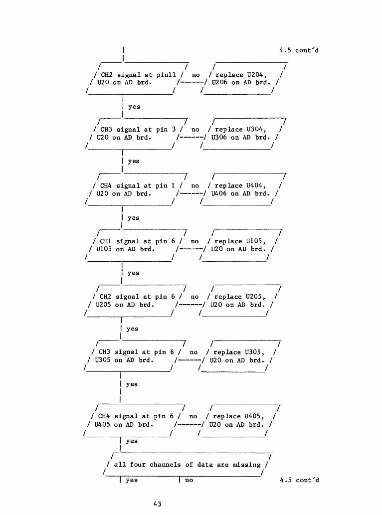
4.5 cont'd
/ II II CH2 signal at pinll / no / replace U204, /
/ U20 on AD brd. / / U206 on AD brd. /
yes
/ / / 7/ CH3 signal at pin 3 / no / replace U304, /
/ U20 on AD brd. / / U306 on AD brd. /
I yes
/ CH4 signal at pin 1 / no / replace U404, // U20 on AD brd. / / U406 on AD brd. /
/ II I
yes
/ II II CH1 signal at pin 6 / no / replace U105, /
/ U105 on AD brd. / / U20 on AD brd. /
II yes
/ CH2 signal at pin 6 / no / replace U205, / / U205 on AD brd. / / U20 on AD brd. /
II yes
/ CH3 signal at pin 6 / no / replace U305, / / U305 on AD brd. / / U20 on AD brd. /
I yes
/ CH4 signal at pin 6 / no / replace U405, / / U405 on AD brd. / / U20 on AD brd. /
I yes
____________________________/ 7/ all four channels of data are missing /
___________ _______________ / I yes I no 4.5 cont'd
43

4.5 cont'dyes no
/ / yes / replace U101 / / CH1 is missing / / U102,U103 on / /____________/ / AD brd. /
I /___________II no
/ / yes / replace U201 / / CH2 is missing / / U202,U203 on / /____________/ / AD brd. /
I /___________/ I no
/ / yes / replace U301 / / CH3 is missing / / U302,U303 on / /____________/ / AD brd. /
I / /no
/ / yes / replace U401 / / CH4 is missing / / U402,11403 on /
/____________/ / AD brd. /
/ SW-1 correctly / no // / installed on AD brd. / / correct switch /
yes
/ check board adressing / no / replace U14 / / at pin 6 U14 on AD brd. / / on AD brd. /
/ III
yes
/ start convert pulse at / no / replace U17, / / pin-12 U19 on AD brd. / / U22 on AD brd. /
yes
/ interrupt pulse on / no / replace U15,U17, / / pin-9 U18 AD brd. / / U18 on AD brd. /
4.5 cont'd
44

I yes 4.5 cont'd
_____I___________________ ___________ / III
I check addressing to AD outputs / no / replace U12 / / pins 7,9-15 U12 on AD brd. / / on AD brd. /
/ III
45

5. BUS LIST
The following pages list the bus connections made to the bus by each board. Although the listings may lead to the impression that that this is an S-100 bus, it is not. Careful attention must be made to the mother-board layout (section 5.1) in order to correctly trace connections. Slot #1 is the power interface board; slot #2 is the analog board; slot #3 is the preamplifier board; slot #4 is the analog-to- digital board, slot #6 is the controller board, and slot #7 is the cartridge controller board.
46

5.1 BUS CONNECTIONS FOR THE MOTHER-BOARD
+5v CART.
+12v CART.
I6 56 6 56 6 56 6 56 6
7 57 7 57 7 57 7 57 7I8 58 8 58 8 58 8 58 8
BRD//1 BRD//2 BRD#3 BRD//4 BRD#5 BRD#6 BRD#7 PIN# PIN# PIN# PIN# PIN# PIN# PIN#1 51 1 51 1 51 1 51 1 51 1 51 1 51 +5v2 2 2 2 2 2 2 +12v
52 52 52 52 52 52 52 -12v3 3 3 3 3 3 3 NU
53 53 53 53 53 53 53 NU4 4 4 4 4 4 4 VIO| 54 54 54 54 54 54 54 -5V
5 55 5 55 5 55 5 55 5 5 5 *CHAanalog55 55 55 NU
6 6 *CHBanalog
56 56 56 NU7 7 *CHCanalog
57 57 57 NU8 8 *CHDanalog
58 58 58 NU9 59 9 59 9 59 9 59 9 9 9 *CHEanalog
-12v I 59 59 59 NUCART. 10 60-10 60-10 60-10 60-10 10 10 *CHFanalog
60 60 60 NURCV 11 61-11 61-11 61-11 61-11 11 11 *CHGanalog
61 61 61 NUXMIT 12 62-12 62-12 62-12 62-12 12 12 *CHHanalog
62 62 62 NUCLK 13 63-13 63-13 63-13 63-13 13 13 *CHIanalog
63 63 63 NURST 14 64-14 64-14 64-14 64-14 14 14 *CHJ analog
64 64 64 NUEXTST 15 65-15 65-15 65-15 65-15 15 15 *CHKanalog
65 65 65 RST CART.INT* 16 66-16 66-16 66-16 66-16 16 16 *CHLanalog
66 66 66 NURST* 17 67-17 67-17 67-17 67-17 17 17 *CHManalog
67 67 67 NU18 18 18 18 18 18 18 jju
68 68 68 68 68 68 68 NU19 19 19 19 19 19 19 NU
69 69 69 69 69 69 69 EXTST20 20 20 20 20 20 20 GND
70 70 70 70 70 70 70 GND21 21 21 21 21 21 21 -5v
7 1 7 1 7 1 7 ]_ 7 1 7 1_____7 1 m22 22 22 22 22 22 22 NU
72 72 72 72 72 72 72 RDY*23 23 23 23 23 23 23 NU
73 73 73 73 73 73 73 INT*24 24 24 24 24 24 24 NU
74 74 74 74 74 74 74 m25 25 25 25 25 25 25 NU
7 5 7 5 7 5 7 5 7 5 7 5 7 5
Continued on next page. NU - Not used
47

5.1 Continued
BRD#1 BRD#2 BRD#3 BRD#4 BRD#5 BRD#6 BRD#7 PIN# PIN# PIN# PIN# PIN# PIN# PIN#
26 26 26 26 26 26 26 NU7 6 7 6 76 7 6 76 76 7 6 NU
27 27 27 27 27 27 27 RCV77 77 77 77 77 77 77 PWR*
28 28 28 28 28 28 28 XMIT78 78 78 78 78 78 78 pDBIN
29 29 29 29 29 29 29 A579 79 7 9 7 9 7 9 79 7 9 A0
30 30 30 30 30 30 30 A480 80 80 80 80 80 80 Al
31 31 31 31 31 31 31 A381 81 81 81 81 81 81 A2
32 32 32 32 32 32 32 NU82 82 82 82 82 82 82 A6
33 33 33 33 33 33 33 Nu83 83 83 83 83 83 83 A7
34 34 34 34 34 34 34 Nu84 84 84 84 84 84 84 NU
35 35 35 35 35 35 35 D0l85 85 85 85 85 85 85 NU
36 36 36 36 36 36 36 DOO8 6 86 86 86 8 6 86 8 6 NU
37 37 37 37 37 37 37 NU87 87 87 87 87 87 87 NU
38 38 38 38 38 38 38 D0488 88 88 88 88 88 88 D02
39 39 39 39 39 39 39 D0589 89 89 89 89 89 89 D03
40 40 40 40 40 40 40 D0690 90 90 90 90 90 90 D07
41 4! 4! 4! 4! 4! 41 DI29 1 9 ! 9 ! 9 ! 9 1 91 9 1 DI4
42 42 42 42 42 42 42 DI392 92 92 92 92 92 92 DI5
43 43 43 43 43 43 43 DI793 93 93 93 93 93 93 DI6
44 44 44 44 44 44 44 Nu94 94 94 94 94 94 94 DI1
45 45 45 45 45 45 45 sOUT95 95 95 95 95 95 95 DIO
46 46 46 46 46 46 46 sINP96 96 96 96 96 96 96 INTA
47 47 47 47 47 47 47 m97 97 97 97 97 97 97 m
48 48 48 48 48 48 48 NU98 98 98 98 98 98 98 NU
49 49 49 49 49 49 49 CLOCK99 99 99 99 99 99 99 Poc*
50-100-50-100-50-100-50-100-50-100-50-100-50-100 GND NU = Not used
48
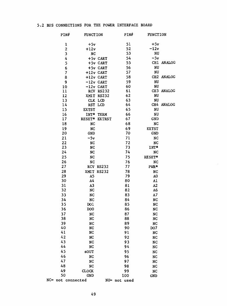
5.2 BUS CONNECTIONS FOR THE POWER INTERFACE BOARD
PIN# FUNCTION PIN# FUNCTION
NC=
123456789
1011121314151617181920212223242526272829303132333435363738394041424344454647484950
+5v+12v
NC+5v CART+5v CART+5v CART
+12v CART+12v CART-12v CART-12v CARTRCV RS232
XMIT RS232CLK LCDRST LCD
EXTSTINT* TERM
RESET* EXTRSTNCNC
GND-5v
NCNCNCNCNC
RCV RS232XMIT RS232
A5A4A3NCNCNC
D01DOONCNCNCNCNCNCNCNC
sOUTNCNCNC
CLOCKGND
>t connected NU=
51525354555657585960616263646566676869707172737475767778798081828384858687888990919293949596979899
100not used
+5v-12v
NU-5vCH1 ANALOGNUNU
CH2 ANALOGNUNU
CH3 ANALOGNUNU
CH4 ANALOGNUNU
GNDNC
EXTSTGNDNCNC
INT*
NCRESET*
NCPWR*
NCAOAlA2A6A7NCNCNCNCNCNC
D07NCNCNCNCNCNCNCNCNC
GND
49

5.3 BUS CONNECTIONS FOR ANALOG BOARD
PIN# FUNCTION PIN#
1234567891011121314151617181920212223242526272829303132333435363738394041424344454647484950
NC= not
+5vNCNCNCNUNUNUNUNUNUNUNUNUNUNUNUGNDNCNCNC
-5vNCNCNCNCNCNCNCA5A4A3NCNCNC
D01DOONC
D04D05D06DI2DI3DI7NC
sOUTsINPNCNC
CLOCKGND
connected
51525354555657585960616263646566676869707172737475767778798081828384858687888990919293949596979899
100NU= not used
FUNCTION
+5vNCNC
-5v CH1 out ANALOGNUNU
CH2 out ANALOGNUNU
CH3 out ANALOGNUNU
CH4 out ANALOGNUNU
GNDNCNCNCNCNC
INT*NCNCNC
PWR*pDBIN
AONCNCA6A7NCNCNCNC
D02 D03 D07 DI4 DI5 DI6 DI1 DIONCNCNC
POC* GND
50

5.4 BUS CONNECTIONS FOR THE PREAMPLIFIER BOARD
PIN# FUNCTION PIN# FUNCTION
1 +5v2 NC3 NC4 NC5 CH1 in ANALOG6 NC7 NC8 CH2 in ANALOG9 NC
10 NC11 CH3 in ANALOG12 NC13 NC14 CH4 in ANALOG15 NC16 NC17 NC18 NC19 NC20 NC21 NC22 NC23 NC24 NC25 NC26 NC27 NC28 NC29 NC30 NC31 NC32 NC33 NC34 NC35 NC36 NC37 NC38 NC39 NC40 NC41 NC42 NC43 NC44 NC45 NC46 NC47 NC48 NC49 NC50 GND
NC= not connected NU= not used
51
51525354555657585960616263646566676869707172737475767778798081828384858687888990919293949596979899100
+5vNCNC
-5vNC
CH1NCNC
CH2NCNC
CH3NCNC
CH4NCNCNCNCNCNCNCNCNCNCNCNCNCNCNCNCNCNCNCNCNCNCNCNCNCNCNCNCNCNCNCNCNCNC
GND
out ANALOG
out ANALOG
out ANALOG
out ANALOG

5.5 BUS CONNECTIONS FOR THE ANALOG-TO DIGITAL BOARD
PIN# FUNCTION PIN# FUNCTION
123456789
1011121314151617181920212223242526272829303132333435363738394041424344454647484950
NC= not
+5vNCNC
VIO*NU
CH1 in ANALOGNUNU
CH2 in ANALOGNUNU
CH3 in ANALOGNUNU
CH4 in ANALOGNUGNDNCNCNCNCNCNCNCNCNCNCNCA5A4A3NCNCNC
D01DOONC
D04D05D06DI2DI3DI7NC
sOUTsINP
NCNC
CLOCKGND
connected NU=
51525354555657585960616263646566676869707172737475767778798081828384858687888990919293949596979899
100not used
+5vNCNC
-5v
NUCH1NUNU
CH2NUNU
CH3NUNU
CH4NUGNDNCNCNCNCNC
INT*
NCNCNC
PWR*pDBIN
AONCNCA6A7NCNCNCNC
D02D03DO 7DI4DI5DI6DI1DIONCNCNCNC
GND
in ANALOG
in ANALOG
in ANALOG
in ANALOG
52

5.6 BUS CONNECTIONS FOR THE CONTROLLER BOARD
PIN# FUNCTION PIN# FUNCTION
123456789
10111213141516171819202122232425262728 29303132333435363738394041424344454647484950
NC= not
+5v+12v
NCVIO*
NCNCNCNCNCNCNCNCNCNCNCNCNCNCNC
GND-5v
NCNCNCNCNC
RCV RS232XMIT RS232
A5A4A3NCNCNC
D01DOONC
D04DOSD06DI2DI3DI7NC
sOUTsINP
NCNC
CLOCKGND
connected
51525354555657585960616263646566676869707172737475767778 798081828384858687888990919293949596979899
100NU= not used
+5vNCNC
-5v
NCNCNCNCNCNCNCNCNCNC
RST CARTNCNCNC
EXTSTGNDNCRDYINT*
NCRESET*
NCPWR*
pDBIN AOAlA2A6A7NCNCNCNC
D02D03D07DI4DI5DI6DI1DIOINTANCNC
POC*
GND
53

5.7 BUS CONNECTIONS FOR THE CARTRIDGE CONTROLLER BOARD
PIN# FUNCTION PIN# FUNCTION
NC=
123456789
1011121314151617181920212223242526272829303132333435363738394041424344454647484950
not
+5vNCNCNCNCNCNCNCNCNCNCNCNCNCNCNCNCNCNCNCNCNCNCNCNCNCNCNCA5A4A3NCNCNC
D01DOONC
D04DOSD06DI2DI3DI7NC
sOUTsINP
NCNCNC
GNDconnected
51525354555657585960616263646566676869707172737475767778798081828384858687888990919293949596979899100
NU= not used
+5vNCNCNCNCNCNCNCNCNCNCNCNCNC
RSTNCNCNCNCNCNCNCNCNC
RESET*NC
PWR*
pDBINAOAlA2A6A7NCNCNCNC
D02D03D07DI4DI5DI6DI1DIONCNCNCNC
GND
CART
54

6. PARTS LIST
6.1 POWER INTERFACE BOARD
value/part// board #
Capacitors
qty notes
O.luf,50v,ceramic C7 10.22uf,50v,ceramic C8,C9 22.2uf,5Ov,ceramic C3,C4 210.Ouf,20v,tantalum C1,C2,C6 3100.Ouf,20v,tantalum C5 1
Centralab CY20C104M Centralab CY20C224M Centralab CY30C225M Sprague CSR13E106KL Sprague CSR13E107KL
Resistors
274 ohm* R3 11.00k ohm R4 13.32k ohm Rl,R2 24.72k ohm R5,R6 2
Semiconductors
1/4 watt, 1%
LT1038Ksteel,12v adj. reg.
UA78M05,+5v reg. UA79M05,-5v reg. 2N2222
lN4001,50v,la
QlQ2Q3Q4,Q5
1112
Linear TechFair childFairchildMotorola
CR1-CR12 11 Motorola
74C10,3-input nand gate Ul
74C30,8-input nand gate U2
CD4724,8-bit latch U3
Fuses
1 National Semiconductor
1 National Semiconductor
1 National Semiconductor
2A Micro 3A Micro
F1,F3-F5 5 F2 1
Littlefuse Littlefuse
Relay
S4E-12V K1,K2 Aromat
55

value/part//
Oscillator
board # qty, notes
251-5907, 2.097152Mhz Yl
Switches
TP11, MOM,SPST T203HMCBE, DPDT
Hardware
SW1 SW2
8 pin, rt. angle,PC 26pin conn.,
rt. angle header 26 pin .Olc, header 13 pin .01, header
PI
P2 P3 P4
14 pin 1C socket 16 pin 1C socket Front mount MTD jack(coax)
Battery holder
Fuse holder
Heat sink
Battery
6-32x1/2" Binder hd 4-40x3/8" Binder hd #6 lock 6-32 hex 4-40 hex
Vectron
C&K C&K
Molex 2391 series
Berg 65823-073 AMP 1-87543-3 AMP 1-87348-3
Augat 314-AG40D Augat 316-AG40D Selectro 50-045-0000
Keystone 856
Littlefuse 281-007
Ahamtor 401-T03
GE GC9B
screwscrewwashernutnut
* R3 adjusted for output of Ql = 5.2volts under load.
56

6.2 ANALOG BOARD
value/part//
Capacitors
board # qty, notes
0.00627 uf,l%, polycarb.
0.0178 uf,l%, polycarb.
0.0267 uf,l%, polycarb.
0.0315 uf,l%, polycarb.
0.0328 uf,l%, polycarb.
0.0387 uf,l%, polycarb.
0.0581 uf,l%, polycarb.
0.1690 uf,l%, polycarb.
470 pf,5Ov,ceramic 0.0015 uf,5Ov,ceramic 0.0047 uf,5Ov,ceramic 0.018 uf,5Ov,ceramic 0.1 uf,5Ov,ceramic 0.22 uf,5Ov,ceramic 0.33 uf,5Ov,ceramic 0.68 uf,5Ov,ceramic 1.5 uf,5Ov,ceramic 2.2 uf,5Ov,ceramic
3.3 uf,5Ov,ceramic 39.0 uf,10v, tantalum 100 uf,10v, tantalum
C8,C17,C26,C35C6,C15,C24,C33C4,C13,C22,C31C2,C11,C20,C29C1,C10,C19,C28C3,C12,C21,C30C5,C14,C23,C32C7,C16,C25,C34
C54,C56C53C52C51C65C66-C90C64C63C62C9,C18,C27,C50,C55,C57C61C60C58,C59,C92,C93
4
4
4
4
4
4
4
4
21111
25111
611
4
Elpac C5B6271F
Elpac C5B1782F
Elpac C5B2672F
Elpac C5B3152F
Elpac C5B3282F
Elpac C5B3872F
Elpac C5B5812F
Elpac C5B1693F
Centralab CW15C471K Centralab CW30C153K Centralab CW20C472K Centralab CW20C183K Centralab CW30C104M Centralab CY20C224M Centralab CY20C334M Centralab CY20C684M Centralab CY30C155M
Centralab CY30C225M Centralab CY30C335M Sprague CSR13E396KL
Sprague CSR13E107KL
57

value/part//
Resistors
board # qty, notes
LOOK, 1/4 watt,
4.70K, 1/4 watt, 1%5.UK, 1/4 watt, 1%10.OK, 1/4 watt, 1%22.IK, 1/4 watt, 1%33.2K, 1/4 watt, 1%47.5K, 1/4 watt, 1%
56.2K, 1/4 watt, 1%82.5K, 1/4 watt, 1%
100.OK, 1/4 watt, 1%
165k, I/ watt, 5%
200k, 1/4 watt, 5%2m, 1/4 watt, 5%
6.8m, 1/4 watt, 5%
on header CM-8: 5.49k, 1/4 watt, 1% 11.3k, 1/4 watt, 1% 26.7k, 1/4 watt, 1%
100K sip network XXK dip network
R1,R12, R23,R34, R85 5 R108 1 R87 1 R84 1 R83 1 R64 1 R70,R72, R75 3 R81,R94 2 R77,R80, R90,R93, R96 5 R62,R63, R65-R67, R74,R86, R104,R105, R109-R112 13 R76,R78, R79,R82, R89,R91, R92,R95 8 R107 1 R71,R73 2 R88 1
R102 R101 R100
RP1 CM1-CM4
Bourne 10-1-104 Bourne 16-1-XX4
value determined by freq. cutoff
58

value/part//
Semiconductors
board # qty, notes
2N2222
1N914
AD7110, audio attenuatorOP421HY, quad op-amp
LI 6 1C J , comparator74C04N, hex inverter74C10, 3 input AND gate74C32, 2input OR gate74C74, dual D flip/flop74C244, octal buffer74C374, octal D flip/flop4012B, 4input NAND gate4029B, U/D binary cntr.4063B, 4bit comparator4066B, quad switch
407 IB, quad NOR gate4521B, 24stage bin. cntr
Switches
SPST momentary4-Position Dip8-Position Dip
Hardware
2x13 .1", header, PC2x3 .1", header, PC1x3 .1", header, PC3 pin rt. ang. header5 pin rt.ang. header
Sockets
8 pin 1C socket14 pin 1C socket16 pin 1C socket20 pin 1C socket
Ql
D3-D6
U22U1-U4 ,U6 ,U7 ,U13,U15,U19U12U9U8U10U24U20U14U27U21,U25UllU16,U17,U18U23U26
SW1SW2SW3
J6,J7J3,J5J4,J8J9J1,J2
1
4
1
71111111111
311
111
22212
11916
2
Motorola
Motorola
Analog Devices
PMISiliconixNational SemiconductorNational SemiconductorNational SemiconductorNational SemiconductorNational SemiconductorNational SemiconductorNational SemiconductorNational SemiconductorToshiba
National SemiconductorNational SemiconductorRCA
C&K // TP11Grayhill //76RSB04SGrayhill #76RSB08S
Amp 1-87543-3AmpAmpAmpAmp
Augat 308-AG40DAugat 314-AG40DAugat 316-AG40DAugat 320-AG40D
59
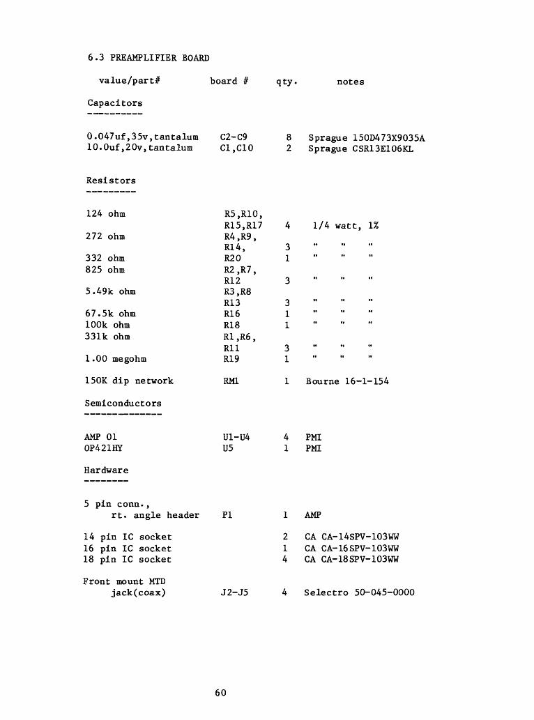
6.3 PREAMPLIFIER BOARD
value/part// board #
Capacitors
qty notes
0.047uf ,3 5v, tantalumlO.Ouf, 2 Ov, tantalum
Resistors
124 ohm
272 ohm
332 ohm825 ohm
5.49k ohm
67.5k ohm100k ohm331k ohm
1 .00 megohm
150K dip network
Semiconductors
AMP 01OP421HY
Hardware
C2-C9C1,C10
R5,R10,R15,R17R4 ,R9 ,R14,R20R2,R7,R12R3,R8R13R16R18Rl ,R6 ,RllR19
RM1
U1-U4U5
82
4
31
3
311
31
1
41
Sprague 150D473X9035ASprague CSR13E106KL
1/4 watt, 1%
tt ti iitt ti ii
ii it H
it ii iiii ii i« M n
M n 11 ii ii
Bourne 16-1-154
PMIPMI
5 pin conn.,rt. angle header PI
14 pin 1C socket 16 pin 1C socket 18 pin 1C socket
Front mount MTDjack(coax) J2-J5
1 AMP
2 CA CA-14SPV-103WW1 CA CA-16SPV-103WW4 CA CA-18SPV-103WW
Selectro 50-045-0000
60

6.4 ANALOG-TO-DIGITAL BOARD
value/part// board #
Capacitors
100 pf,100v,ceramic
0.OOluf,lOOv,ceramic 0.22 uf,5Ov,ceramic
2.2 uf,5Ov,ceramic
0.01 uf,l% polycarb.
100.0 uf,10v,tantalum
Resistors
C56-C59
C16,C17
qty,
C1,C4,C20,C33C29C3,C5-C15,C19,C21-C28,C30,C32,C34-C44,C46-C55,C60-C62C2,C18,C31,C45
41
44
4
notes
Centralab CN15A101K Centralab CN20A102K
Centralab CY20C224M
Centralab CY30C225M
Elpac PD5A103K
Sprague CSR13E107KL
332, 1/4 watt, 1% 1.00k, 1/4 watt, 5%
3.32k, 1/4 watt, 1%4.42k, 1/4 watt, 1%10.0k, 1/4 watt, 5%
20.0k, 1/4 watt, 1%
100k, 1/4 watt, 1%
200k, 1/4 watt, 1%
R18,R19 2R101,R201,R301,R401 4R17,R20 2R16,R21 2R11,R104,R204,R304,R404 5R103,R203,R303,R403 4R12-R15,R22,R23,R105-R108,R205-R208,R305-R308,R405-R408, 22R102,R202,R302,R402,R109,R209,R309,R409 8
61

value/part//
Semiconductors
2N2907
1N914
OP21EP,Op-amp
board # qty, notes
ADC1210HCD, A-D convert
7541KN, 12bit D-A
L161CJ, comparator
CD4016BE, analog switch CD4017BE, counter CD4028B,loflO decode
CD4029, counter
CD4040, counter CD4043, latch CD4063, 4-bit compare CD4536, timer 74COO, NAND gate
74C04, hex inverter 74C08, AND gate
74C10, NAND gate 74C138, Iof8 decode 74C374, latch
Ql
Dl
U104,U105,U204,U205,U304,U305,U404,U405U101.U201,U301,U401U106,U206,U306U406U111.U211,U311,U411U20U17U107,U207,U307U407
U108,U208,U308U408U22U18U14U15U110,U210,U320,U410U19U21.U109,U209,U309,U409U16U12U13.U102,U103,U202,U203,U302,U303,U402,U403
1
1
8
4
4
411
4
41111
41
511
9
Motorola
Motorola
Precision Monolithics
National Semiconductor
Datel
SiliconixRCARCA
Fairchild
FairchildFairchildToshibaToshibaRCA
National SemiconductorNational Semiconductor
National SemiconductorNational SemiconductorNational Semiconductor
Motorola
Switches
4-Position Dip SW1 1 Grayhi11 76RSB04S
62
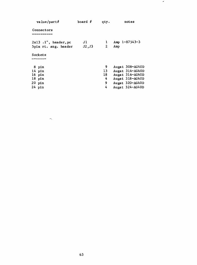
value/part//
Connectors
board # qty notes
2x13 .1", header,pc Jl 5pin rt. ang. header J2,J3
Sockets
8 pin 14 pin 16 pin 18 pin 20 pin 24 pin
1 Amp 1-87543-32 Amp
9 Augat 308-AG40D13 Augat 314-AG40D18 Augat 316-AG40D
4 Augat 318-AG40D9 Augat 320-AG40D4 Augat 324-AG40D
63

6.5 CONTROLLER BOARD
value/part// board #
Capacitors
qty notes
0.22 uf,5Ov,ceramic 39.0 uf,10v,tantalum
100.0 uf,10v,tantalum
Resistors
1.00k, 1/4 watt, 5% 10.0k, 1/4 watt, 5%
27.4k, 1/4 watt, 5%50.0k, 1/4 watt, 5%68.1k, 1/4 watt, 1%
100k network
C4-C31ClC2,C3
R5R1,R6,R7,R12,R13R8,R9RIORll
RP1
2812
Centralab CY20C224M Sprague CSR13E396KL Sprague CSR13E107KL
Bournes 10-1-104
Semiconductors
1N914 D1-D4
74COO, NAND gate U2074C02, NOR gate U1274C08, AND gate U1374C30, NAND gate U2874C32, OR gate U22,U2774C74*, flip/flop U2674C86*, XOR gate U2574C138, Iof8 decode U23,U2474C240, octal buffer U2174C244, octal buffer U18,U1974HC373, latch U1758167A, RTC U10NSC800N, CPU U7NSC810AN,I/0 ram timer U8CD4040, counter U14HM5-6564, ram U2-U6MBM27C64-30,EPROM U16OP220HZ, op-amp U15
4 GE
1 National Semiconductor1 National Semiconductor1 National Semiconductor1 National Semiconductor2 National Semiconductor1 National Semiconductor1 National Semiconductor2 National Semiconductor1 National Semiconductor2 National Semiconductor1 National Semiconductor1 National Semiconductor1 National Semiconductor1 National Semiconductor1 Fairchild5 Harris1 Fujitsu1 PMI
* not needed for some Software, tied together in place of U25.
Use 14 pin dip header with pins 2&3, 5&6
64
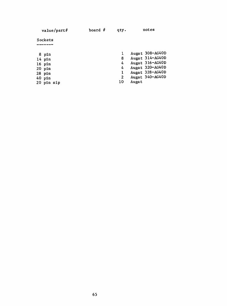
value/part// board # qty. notes
Sockets
8 pin 1 Augat 308-AG40D!4 pin 8 Augat 314-AG40D16 pin 4 Augat 316-AG40D20 pin 4 Augat 320-AG40D28 pin 1 Augat 328-AG40D40 pin 2 Augat 340-AG40D20 pin sip 10 Augat
65

6.6 CARTRIDGE CONTROLLER BOARD
value/part# board #
Capacitors
qty notes
100.0 pf,100v,mica C20,C21,C23 3
0.10 uf,100v,ceramic C4-C19,C22 17
47.0 uf,16v,electrolytic C1-C3 3
Resistors
CT1000PF
CF.1@100Mar am CFTE-113
100, 1/4 watt, 5% 2.0k, 1/4 watt, 5%
2.0k network 220/330 network
R4,R5 R1-R3
M1,M24 M3,M8
Bournes 10-1-202 Beckman 785-5-R220/330
Crystal
QC6.144MHZ CL1
Semiconductors
74LS04, hex inverter 7406, hex inverter 74LS10, NAND gate 74LS11, AND gate
74LS74, flip/flop
74LS138, 74LS155, 74LS240, 74LS244, 74LS287, 74LS368, 74LS373, 74LS374,
Iof8 decode dual 2/4 decode octal inverter octal buffer CODEC rom hex buffer latch octal flip-flop
2114-2, ram !Kx4 2651, prog, interface 2716, EPROM 2Kx8 6132-6WB, ram 4Kx8 8085, CPU
M34M10M21,M22M20,M35,M36M15,M23,M31M18,M19M26M4,M9M11-M13M25M30M2M5,M6,M32,M33M16,M17M7M29M27,M28Ml 4
112
3
32123111
421121
Texas InstrumentsFairchildFairchild
Fairchild
Texas InstrumentsTexas InstrumentsFairchildTexas InstrumentsTexas InstrumentsSigneticsTexas InstrumentsTexas Instruments
Texas InstrumentsNECSigneticsHatachiZiglogNEC
66

value/part// board # qty. notes
Sockets
14 pin 10 Augat 3U-AG40D16 pin 8 Augat 316-AG40D18 pin 2 Augat 318-AG40D20 pin 10 Augat 320-AG40D24 pin 1 Augat 324-AG40D28 pin 2 Augat 328-AG40D40 pin 1 Augat 340-AG40D
Switches
4-Position Dip SW1 1 Grayhill 76RSB04S
Connectors
40 pin header P2 150 pin header PI 12x3 pin header 1
67

REFERENCES
Ambuter, B.P., 1979, Low cost, low power binary gain range amplifier operates over a wide dynamic range: Electronics Design: Feb. 1, 1979, p. 90-91.
Ambuter, B.P., and Davis, R.E., 1981, Geophysical data acquisition in remote environments: U.S. Geological Survey Open-File Report 81-1083, 28p.
Ambuter, B.P., and Godley, J.H., 1983, A flexible low-power data- acquisition system, in Meyer, R.P., and others, Proceedings of the workshop on portable digital seismograph development: Int'l. Assoc. Seismology and Phys. Earth's Int., Comm. Controlled Source Seismology, p. 32-42.
Elmquist, K.A., Fullmer, H., Gustavson, D.B., and Morrow, G., 1979, Standard specification for S-100 bus interface devices: IEEE Task 696.1: Computer, vol. 12, no. 7, p. 28-51.
Fredricks, J.J., Evenden, G.I., and Dodd, J.E., 1985, Shipboard playback for Ocean Bottom Instrument Package, Modification II: U.S. Geological Survey Open-File Report 85-111, 69 p.
Miller, G.K., 1986, Ocean Bottom Seismometer (OBS) software, Modification III: U.S. Geological Survey Open-File Report 86-269, 130 p.
U.S. Geological Survey, 1984, Major electronic circuits and components of the Ocean Bottom Instrument Package (OBIP): U.S. Geological Survey Open- File Report 84-267, 69 p., 21 sheets.
68

APPENDIX I
Electrical Specifications
Data channels Time channels Dynamic range
Main converterGain rangingTotalanalog-to-digital noiseTotal useful
Gain range rateTypeIncrementRateSample rate
FiltersTypeFrequencyRoll off
MemoryMainBufferProgram memory
Power requirements
Functional Specifications
Event recording CriteriaLTA time constant STA time constant
Threshold
Operational range Program window
Number of windowsTurn-on delayNumber experiments/window
Window spacing
Offset
1 to 41
72dB (12bits)60dB (lObits)132dB150 millivolts90dB (15bits)
floating 6dB/step 7 microseconds 1, 2, 4, 8 milliseconds
software selectable
butterworth30, 60, 125, 250, 500 Hz48dB/octave
8 kilobytes32 kilobytes
8 kilobytes
+12 volts, 85 milliamps -12 volts, 1 milliamp
long term vs short term 5 minutes50 milliseconds to 0.5 seconds
software selectable 6 to 24dB
software selectable 70dB
software selectable 1 to 9999
software selectable 1 to 99minutes
software selectable 0 to 99 seconds
software selectable
69

Cartridge Recorder SpecificationsData capacity 17.5 Megabytes Density 6400 BPI Number of tracks 4Power Requirement +12 volts, 0.5 amps
(maximum values) -12 volts, 0.5 amps+5 volts, 2.25 amps
70

FIGURES
71

LOWPASS FILTERANALOG BOARD
ANALOG INPUT
PREAMP BOARD
A-D BOARD
DECODE LOGIC
LATCH
OFF REN
Nx"SET IOVAL
ADC
CF
IS m *JL^"7 m*^m
SAIN- ?IANGE SAMPLE
& HOLD
i i
LATCH
ADCi i
LATCH
1
ADCi i
LATCH
D
CPU 40K RAM 8K EPROM CLOCK DECODE
LOGIC
CPU BOARD
CARTRIDGE CONTROLLER BOARD
BATTERY
FIGURE 1. Block Diagram of the Geophysical Data-Acquisition System
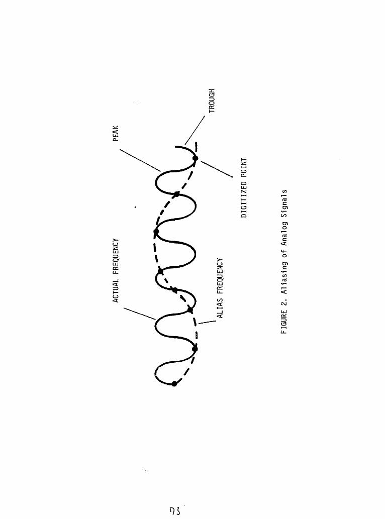
ACTU
AL FREQUENCY
PEAK
TROU
GHAL
IAS
FREQUENCY
DIGI
TIZE
D PO
INT
FIGU
RE 2
. Aliasing o
f An
alog
Sig
nals

SWIT
CHCONTROL
LOGI
C
FEED
BACK
L _
rrcH
1>
< \i / fr i
> i i
\l
AM
PLI
FIE
R
LON
G-T
ERM
AV
ERAG
ER
i
(,\ L
DATA
2-
30 H
z
EVEN
T CO
MPAR
ATOR
SHORT-TERM
AVER
AGER
* EV
ENT
ENAB
LE
THRE
SHOL
D AD
JUST
FIGU
RE 3. Block
Diag
ram
of E
vent
-Det
ecti
on C
ircu
itry
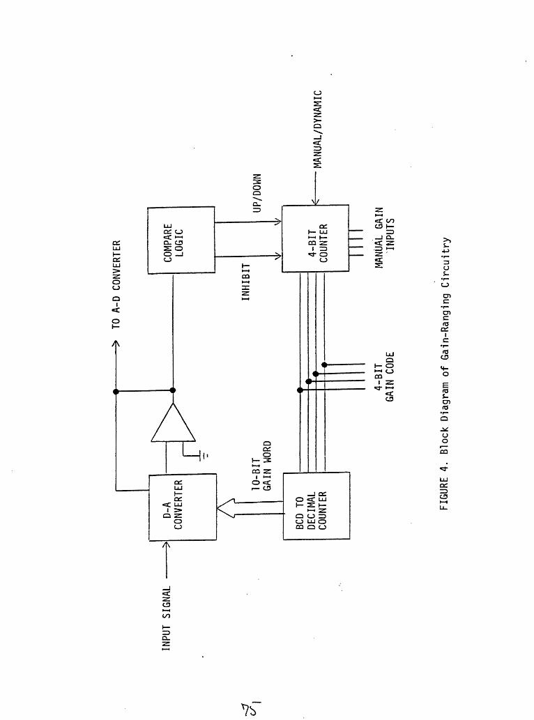
INPUT
SIGN
AL
10-B
IT
GAI
N
WOR
D
BCD
TODECIMAL
COUNTER
->
TO A
-D C
ONVE
RTER
4-BIT
GAIN CO
DE
COMP
ARE
LOGIC
INHI
BIT
UP/DOWN
4-BI
T CO
UNTE
RMANUAL/DYNAMIC
MANU
AL GA
IN
INPU
TS
FIGU
RE 4
. Block
Diag
ram
of G
ain-Ranging
Circuitry

LJ LJ
CARTRIDGE CONTROLLER CPU
A-D
PREAMP ANALOGPOWER INTERFACE
FIGURE 5. Location of Circuit Boards on the Bus

EARLY TERMINATION BUTTON
TERMINAL CONNECTOR ( RS232 )
POWER CONNECTOR
Icllt^oooo loooooooo
SATELLITE CLOCK CONNECTION
RESET BUTTON
FIGURE 6. User Connections and Controls

POW
ER
CONN
ECTI
ON
oooo
CONT
ROLL
ER
BOAR
D RE
SET
X_
__
__
__
__
_
IIII
IIII
IIII
IIII
IIII
IIII
IJII
III
+5v
RELAY
+12v
AND
-12v RELAY
lf\'
sD0.5 D» 0*
r- OSC
ILLA
TOR
ADJU
STME
NT
OSCI
LLAT
OR T
EST
POINT
FIGU
RE 7
. Component
Layo
ut o
f th
e Po
wer
Inte
rfac
e Board
SCA
LE:
/ '/
AP
PR
OV
ED
BY
DR
AW
ING
N
UM
BE
R

FILTER T
EST/
POINTS~
X
ANAL
OG INPUT
\JU
MPE
R PA
DSFO
R EV
ENT
DET
ECTI
ON
JEST POINTS
FOR
EVEN
T DETECTION
HEADERS
FOR
FILTERS
C13
FILTER O
UTPU
TSIlll
llllllll
llllllll
llllTE
ST POINT
FOR /
EVEN
T DE
TECT
ION
BOAR
D AD
DRES
SING
SW
ITCH
GND
VOLT
AGE
TEST
-5v
POIN
TS
+5v
REMO
VE FOR
EVEN
T TE
STIN
G
INST
ALL
FOR
EVEN
T TE
STIN
G
FIGU
RE 8
. Component
Layo
ut o
f th
e An
alog
Bo
ard
5CM.
E-
/ '
/A
PP
RO
VE
D B
Y
CM
AR
RE
TT
l P
RO
-FO
B*
»10»>
P
RIN
TE
D
ON
»2
OM
C
HA
RP
RIN
T
VE
LL
UM
GK
m
DR
AW
ING
NU
MB
ER

HORI
ZONT
AL
1 HO
RIZO
NTAL
2
ANAL
OG OUTP
UTS
+5v
TEST
PO
INT -^
-5v
TEST
- POINT
ci
GEOP
HONE
\ n
1
GEOPHONE
\n
VERT
ICAL
GEOPHONE
nHY
DROP
HONE
Illlll
llllll
llllll
llllll
llllll
llllll
llllll
llllll
lll
TED ON t»M CHARPRINT VELLUM
FIGURE 9.
Component
Layout o
f the
Prea
mpli
fier
Board
SCAL
E.
/ '/
DA
TE:
?
AP
PR
OV
ED
BY
DR
AW
ING
NU
MB
ER

BOARD
ADDRESS/
SWITCH'
s.cs
>
^ w
E
5D
« O
^
rn
rS,
O tt o ^
cil
,%
*
rSI*
11
JP>
DIE
c!»C
ED
»
JPI
ji
/Nfi/
r *e
teer
r©n
Oo
O s K no o
ANAL
OG
IN
PUTS
W
Ql O iO:
j- 80 \jito
_ y/z
C35
Illlllll
llllllll
llllllll
l
VOLTAGE
TEST
POINTS
FIGURE 1
0. Component
Layout o
f th
e An
alog
-to
-Dig
ital
Board
SC
ALE
. /
/
p 2
TE
D
ON
I2
0H
C
HA
BP
SIN
l V
tLL
LJ
Bo
AP
PR
OV
ED
B
Y
DR
AW
ING
NU
MB
ER

00 r*
VO
LTA
GE
TE
ST
POII
1TS
-5v
GN
D
+5v
SATELLITE CLOCK CONNECTOR
p^
«n C
ED
**C
Z)«
C3'
(
£*_!;
cV
l tjj
0
_
CJO
_Q_
^
_Q
J/27
\Wl
O
UH
£17
~~
oc
I// 2
C2(
r0
UUUU
UUU
C2
f «1
H0
0
nn
nn
nn
nn
I
I'uu
uuuu
uurJ
>'
nm'f
buu
i//n
!=
)
C"
Oc/
o
OO
O
O
Illlllll
llllllll
llllllll
llllllll
llllllll
llllllll
ll
EPROM
FIGU
RE 11
. Component Layout of th
e
Controller Board
8 Wi tb
AP
PR
OV
ED
B
Y
CH
AR
RE
TT
E
PR
O-F
OR
M «
OP
»
PR
INT
ED
O
N
»JO
M
CM
AR
PR
INT
V
EL
LU
M
DR
AW
ING
NU
MB
ER

oC
*'2
'-/Z
' -f
t*
I <
«, t
Q00
000m
m
n
H
2
Tn*«
*X/
H.T
-QH
D *
""r
ren
-to-
-QE
D
i J
n
> ,
>*' /X
A
81
T J i LK
c 1 c
I c 1
/* Bl
i >
*y M
H it i
H3
^l
Q - C r, I \ s \fS
In
1 JT fJ 1 -r
V r
1
1
J 1
L,. ( rf Q
Z r ii r*3
f"
1'
rcT
u(
Ti
^'^
-'
' 1 *
^"^
«>l
»J-
-14
I*t
i
^x»
L_
. N <
1 1
-W- ~. !L K
T 0 1
* >5
1 '
^ l". r
^
!»,
_'j
1 «
«ll
EH h.«
. <
] <
1 (
<>c
*{,
<
...H n
:«
rs ! 1 1
<
J
«*! "~
"23
**
* ^
1 5"
-£|»
^«-i£.
l++
^+*L
1 V
wV
k'l
L_
i
eft 1
0
i , Cl
1 1
-<i
7* Q
V
" 3
__ "
|
i
or
J-
/?;
DB.U
S
Figu
re 12
. Schematic
of t
he P
ower Interface
Board
TITL
E

FIGU
RE 1
3. Sc
hema
tic
of t
he E
vent
-Det
ecti
on C
ircu
its

FREA
mP
&»IWD
fc,
oC
FIGURE 1
4. Sc
hema
tic
of t
he P
ream
plif
ier
Board
and
the
Anti-Aliasing
Filt
ers
on t
he A
nalo
g Board

/3
(T
(JNA
LOG
(A/
J |
T-V
-. «
iiM
il
Do
KW
7
_ r
r-77
-i £3
!
71
[
/_«
' C
» O
X 0 U
/7
A
,f - »
FIGU
RE 1
5. Sc
hema
tic
of t
he A
nalo
g-to
-Dig
ital
Bo
ard
Channel
1 an
d Ti
ming
Circuits
TITL
EBo
**t>
SHE
£T I
or
3

FIGURE 1
6. Sc
hema
tic
of t
he A
naloq-to-Diaital Board
Chan
nels
2+
3

DI7
-Sv
FIGU
RE 1
7. Sc
hema
tic
of t
he A
nalog-to-Digital
Board
Channel
4 Ci
rcui
tsTI
TLE
fl-p
Snee
r
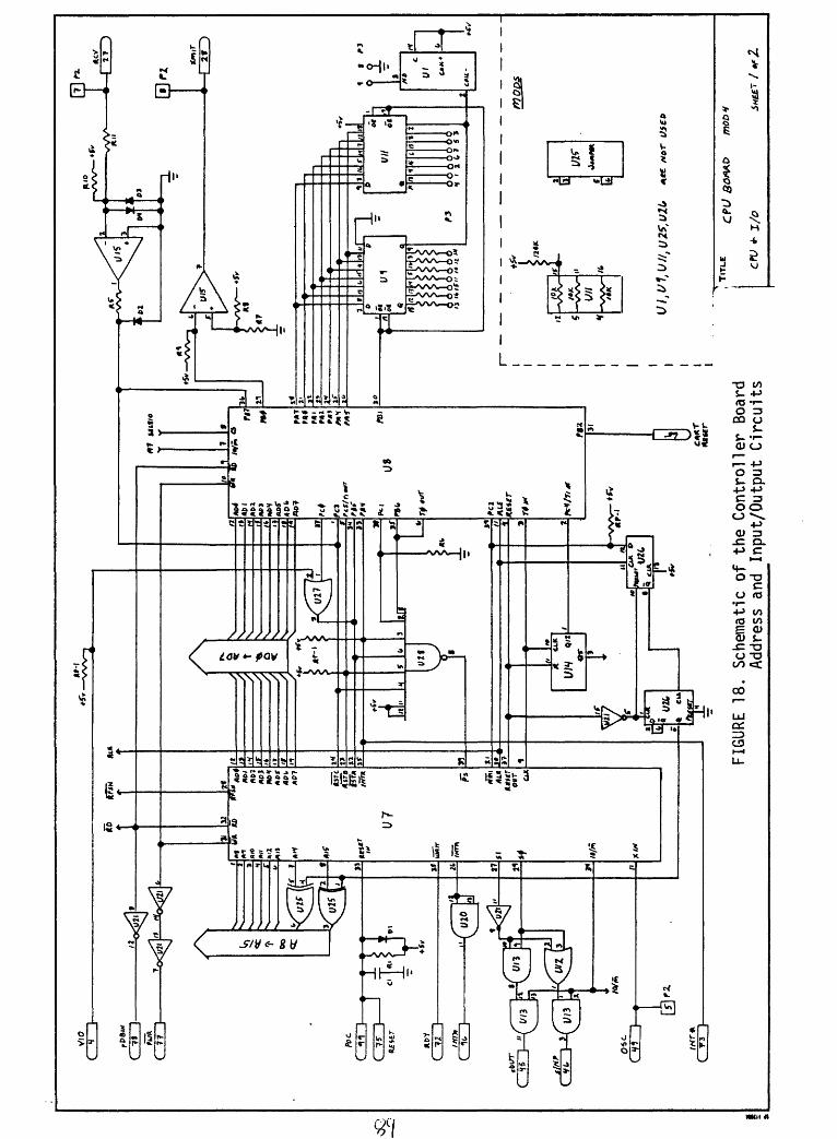
FIGU
RE 1
8. Sc
hema
tic
of t
he C
ontr
olle
r Board
Addr
ess
and
Inpu
t/Ou
tput
Cir
cuit
sCPU + 1/0
Sn££7 /

*?5*
ALE W*
T^
1 Pi
tteu
r
r
FIGU
RE 1
9. Schematic
of t
he C
ontroller
Boar
dMe
mory
Cir
cuit
s