AN4877, PROFIBUS on QUICC Engine Block · PROFIBUS on the QUICC Engine Block, Rev. 1 2 Freescale...
24
Freescale Semiconductor Application Note © 2014 Freescale Semiconductor, Inc. All rights reserved. PROFIBUS is a fieldbus protocol defined in the IEC 61158 standards. It uses RS-485 UART for the physical layer at rates up to 12 Mbaud. The layer 2 MAC is typically implemented in an ASIC. However, on the QUICC Engine microcode assumes this function for both PROFIBUS master and slave modes. This application note explains the baud rate clocking, physical layer connectivity, initialization, configuration, and control of a UCC UART programmed for the PROFIBUS mode of operation. It is aimed at hardware and low-level software developers and is relevant for the following devices: • QorIQ P1012, P1016, P1021, and P1025 • PowerQUICC MPC8306 and MPC8309 • QorIQ Layerscape LS1020A & LS1021A This application note is supplemental to the PROFIBUS microcode user’s manual in the QEIWRM specification and the data sheet of the target device. It is recommended that these instructions are followed in order to develop a conformant PROFIBUS master or slave on applicable QorIQ and PowerQUICC devices. Document Number: AN4877 Rev. 1, 12/2014 Contents 1. Baud rate generation and timers . . . . . . . . . . . . . . . . . 2 2. Using multiple peripherals in PROFIBUS mode . . . . 6 3. UCC UART physical layer recommendations . . . . . . 8 4. Enabling idle transmit mode . . . . . . . . . . . . . . . . . . . 14 5. Memory resources . . . . . . . . . . . . . . . . . . . . . . . . . . . 17 6. TWR-P1025 disclaimer . . . . . . . . . . . . . . . . . . . . . . 19 A. GPIO configuration example code . . . . . . . . . . . . . . 20 PROFIBUS on the QUICC Engine Block
-
Upload
phamnguyet -
Category
Documents
-
view
230 -
download
0
Transcript of AN4877, PROFIBUS on QUICC Engine Block · PROFIBUS on the QUICC Engine Block, Rev. 1 2 Freescale...

Freescale SemiconductorApplication Note
© 2014 Freescale Semiconductor, Inc. All rights reserved.
PROFIBUS is a fieldbus protocol defined in the IEC 61158 standards. It uses RS-485 UART for the physical layer at rates up to 12 Mbaud. The layer 2 MAC is typically implemented in an ASIC. However, on the QUICC Engine microcode assumes this function for both PROFIBUS master and slave modes.
This application note explains the baud rate clocking, physical layer connectivity, initialization, configuration, and control of a UCC UART programmed for the PROFIBUS mode of operation. It is aimed at hardware and low-level software developers and is relevant for the following devices:
• QorIQ P1012, P1016, P1021, and P1025• PowerQUICC MPC8306 and MPC8309• QorIQ Layerscape LS1020A & LS1021A
This application note is supplemental to the PROFIBUS microcode user’s manual in the QEIWRM specification and the data sheet of the target device. It is recommended that these instructions are followed in order to develop a conformant PROFIBUS master or slave on applicable QorIQ and PowerQUICC devices.
Document Number: AN4877Rev. 1, 12/2014
Contents1. Baud rate generation and timers . . . . . . . . . . . . . . . . . 22. Using multiple peripherals in PROFIBUS mode . . . . 63. UCC UART physical layer recommendations . . . . . . 84. Enabling idle transmit mode . . . . . . . . . . . . . . . . . . . 145. Memory resources . . . . . . . . . . . . . . . . . . . . . . . . . . . 176. TWR-P1025 disclaimer . . . . . . . . . . . . . . . . . . . . . . 19A. GPIO configuration example code . . . . . . . . . . . . . . 20
PROFIBUS on the QUICC Engine Block
PROFIBUS on the QUICC Engine Block, Rev. 1
2 Freescale Semiconductor
Baud rate generation and timers
1 Baud rate generation and timersThe PROFIBUS controller on the QUICC Engine block uses the UART MAC of the UCC. The UART MAC uses an 8 times oversampling rate on the asynchronous UART interface. Therefore, the Baud Rate Generation (BRG) clock must be 8 times the baud rate used on the PROFIBUS network.
This table provides example baud rates and their corresponding BRG clock outputs.
The BRG clock source can be derived from an external or internal source.
1.1 Externally sourcing BRG clocksThe BRG input clock can be sourced externally using a GPIO pin that supports CLKx input functionality. When using an externally sourced clock as the input to the BRG_CLK, the maximum frequency is 50 MHz. This option can support baud rates up to a maximum of 6 Mbaud when using an external 48 MHz oscillator to clock the BRG.
1.2 Internally sourcing BRG clocksThe BRG input clock can also be sourced internally. Consider the following example:
For a 12 Mbaud operation with a 96 MHz clock supplied to the UCC, the SYSCLK source frequency and platform multiplier must yield a BRG_CLK frequency that is a multiple of 96 MHz.
If the SYSCLK is 64 MHz and the platform multiplier of 6 yields a 384 MHz QUICC Engine clock, then the BRG input clock is 192 MHz.
When selecting the SYSCLK, ensure the following:• The combination of the SYSCLK source clock frequency and the platform/QE multiplier results in
at least the minimum QUICC Engine frequency and no greater than the maximum QUICC Engine frequency.
• The QUICC Engine frequency, derived from the product of SYSCLK and factor (platform multiplier), is an integer multiple of 96 MHz
• The SYSCLK selection allows acceptable frequency configuration of other elements on the SoC, such as the CPU and bus.
NOTEThe LS1020/21 has an option to source the BRG input clock from the platform clock or the QUICC Engine clock divided by 2. The user must use the platform clock. The QUICC Engine clock divided by 2 does not yield a multiple of 96MHz on these devices.
Table 1. Baud rates and corresponding BRG clock outputs
Operation baud rate BRG output clock
12 Mbaud 96 MHz
9600 baud 76.8 kHz
PROFIBUS on the QUICC Engine Block, Rev. 1
Freescale Semiconductor 3
Baud rate generation and timers
This table details the range of clock and frequency values supported according to the data sheet of each device.
1.3 Controlling IEC timersThe IEC PROFIBUS specification (61158-4-3) describes numerous timers that affect state transitions on the PROFIBUS master and slave state machines. Because PROFIBUS supports a variety of baud rates, the IEC specification describes these timers as a number of bits. For example, the minimum TSDR timer controls the duration, in bits, that a node waits before transmitting a response to a request frame. In fast systems, this can be set as low as 11 bit times (1 UART character).
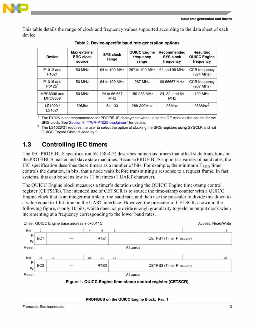
The QUICC Engine block measures a timer’s duration using the QUICC Engine time-stamp control register (CETSCR). The intended use of CETSCR is to source the time-stamp counter with a QUICC Engine clock that is an integer multiple of the baud rate, and then use the prescaler to divide this down to a value equal to 1 bit time on the UART interface. However, the prescaler of CETSCR, shown in the following figure, is only 10 bits, which does not provide enough granularity to yield an output clock when incrementing at a frequency corresponding to the lower baud rates.
Table 2. Device-specific baud rate generation options
DeviceMax external BRG clock
source
SYS clock range
QUICC Engine frequency
range
Recommended SYS clock frequency
Resulting QUICC Engine
frequency
P1012 and P1021
50 MHz 64 to 100 MHz 267 to 400 MHz 64 and 96 MHz CCB frequency (384 MHz)
P1016 and P01251
1 The P1025 is not recommended for PROFIBUS deployment when using the QE clock as the source for the BRG clock. See Section 6, “TWR-P1025 disclaimer,” for details.
50 MHz 64 to 100 MHz 267 MHz 66.66667 MHz CCB frequency(267 MHz)
MPC8306 and MPC8309
50 MHz 24 to 66.667 MHz
150-233 MHz 24, 32, and 64 MHz
192 MHz
LS1020 / LS1021
50Mhz 64-133 288-300Mhz 96Mhz 288Mhz2
2 The LS1020/21 requires the user to select the option of clocking the BRG registers using SYSCLK and not QUICC Engine Clock divided by 2.
Offset QUICC Engine base address + 0x0011C Access: Read/Write
Bits 0 1 4 5 6 15
REC1 — RTE1 CETPS1 (Timer Prescale)
W
Reset All zeros
Bits 16 17 20 21 22 31
REC2 — RTE2 CETPS2 (Timer Prescale)
W
Reset All zeros
Figure 1. QUICC Engine time-stamp control register (CETSCR)

PROFIBUS on the QUICC Engine Block, Rev. 1
4 Freescale Semiconductor
Baud rate generation and timers
PROFIBUS is required to support the following baud rates:• 12 M, 6 M, 3 M, 1.5 M, 500 k, 187.5 k, 93.75 k, 45.45 k, 19.2 k, 9.6 k
Commonly used baud rates less than 100 k are not supported using the CETSCR prescaler directly. There is not sufficient granularity to achieve a timer output with a value equal to 1 bit time at these lower baud rates. As a result, the microcode must provide the increased granularity.
The PROFIBUS microcode supports a scaling_factor parameter for scaling the 12 MHz output. This is used to calculate the time-out values for the IEC timers. For example, if the system uses a baud rate of 1.5 M, then the scaling_factor is 12 M / 1.5 M = 8. The number of bits for an IEC timer is multiplied by the scaling_factor parameter to augment the CETSCR output to a value coherent with the baud rate being used. Taking the previous example where the minimum TSDR is 11 bits, the microcode waits 88 (11*scaling_factor) increments of CETSCR before declaring this timer has expired at 1.5 Mbaud.
Recommended best practice: Program the CETSCR[CETPS1] to output a 12 MHz clock so each increment is 1 bit time at 12 Mbaud.
1.3.1 Recommended operating frequenciesBecause CETSCR must be used for IEC timers, the QUICC Engine clock must always be a multiple of the baud rate. Otherwise, IEC timing functions could be inaccurate.
The recommended operating frequencies for QUICC Engine block in PROFIBUS mode are:• 192 MHz• 288 MHz• 384 MHz
If the QUICC Engine clock is 192 MHz or 384 MHz, the lowest baud rate supported using CETPS1[TimerPrescale] is 187.5 kbaud or 375 kbaud, respectively.
These QUICC Engine clock frequencies work well with all of the commonly used PROFIBUS baud rates. They also work well for the UART’s physical oversampling rate that is programmed in the BRG register.

PROFIBUS on the QUICC Engine Block, Rev. 1
Freescale Semiconductor 5
Baud rate generation and timers
1.4 Configuration for recommended operating frequencies The following table details the recommended QUICC Engine, BRG and CETSCR frequencies for each device family.
The table below indicates which scaling factor to use with each baud rate.
Table 3. Operating frequencies and associated configuration
P10xx MPC830x LS1020/21
QUICC Engine frequency
384MHz 192MHz 288MHz
BRG frequency 192MHz1
1 The BRG frequency is the QUICC Engine clock divided by 2.
96MHz1 288MHz2
2 The BRG frequency must be programmed to be sourced from the platform clock by setting BRGCn[EXTC] = 0b01
CETSCR1[ECR]3
3 Must be programmed to generate a timestamp counter incrementing at a frequency of 12MHz
30 14 22
brg_freq_enum4
4 This is a microcode parameter resident in the UCC PROFIBUS parameter RAM
2 1 3
Table 4. Scaling factors
Baud rate scaling_factor1
1 This is a microcode parameter resident in the UCC PROFIBUS parameter RAM, it is calculated as follows: (BRGCn[CD] + 1) / (BRG_Frequency / 96M).
12M 1
6M 2
3M 4
1.5M 8
500k 24
187.5k 64
93.75k 128
45.45k 264
19.2k 625
9.6k 1250
PROFIBUS on the QUICC Engine Block, Rev. 1
6 Freescale Semiconductor
Using multiple peripherals in PROFIBUS mode
2 Using multiple peripherals in PROFIBUS modeThe following can preclude the usage of other QUICC Engine peripherals when the PROFIBUS mode of operation is enabled:
• PROFIBUS nodes that respond to send/request frames are required to respond deterministically• Dual port performance
The QUICC Engine block processes requests from enabled peripherals in round-robin style. If the user enables another QUICC Engine peripheral, such as a UCC Ethernet controller, this peripheral may be serviced directly before the timer for sending a response expires. This may lead to excessive response jitter, especially at the higher baud rates (> 1.5 M). Enabling two UARTs in PROFIBUS mode may lead to performance issues at the higher baud rates. This is more prevalent on devices that have a relatively low QUICC Engine frequency.
For example, the MPC8306, as seen in Table 2, requires a QUICC Engine block running at 192 MHz. This is approximately one instruction executed every 5 ns. At 12 Mbaud each bit is received 83 ns apart. The QUICC Engine UART generates a request for every UART character. For PROFIBUS, each 8 bits of data translates into 11 bits on the physical interface. Resultantly, the UART generates a request every 830 ns on the UCC receiver. This yields 166 (830 ns/5 ns) clocks/instructions. However, the transmitter also needs to be serviced. Assuming that the transmitter takes half the allotted cycles, this is 83 clocks for UCC Rx and 83 clocks for the UCC Tx. Adding another port yields approximately 42 clocks per port, which can lead to performance issues, increased latencies, and increased jitter.
This table provides device recommendations based on the protocols used and interface recommendations.Table 5. Device recommendations
Number of PROFIBUS
ports
PROFIBUS baud rate
Fast EthernetOther QUICC
Engine peripheral(s)
Recommendation
1 12 Mbaud No No Use any device.
1 > 6 Mbaud Yes No Use a device with a hardware Ethernet block, for example a P10xx or LS10xx device.
1 ≤ 6 Mbaud Yes No Contact your local Freescale representative for assessment of the performance and feasibility of your requirements.
1 up to 12 Mbaud No Yes Contact your local Freescale representative for assessment of the performance and feasibility of your requirements.
1 ≤ 6 Mbaud Yes Yes Use a device with a hardware Ethernet block, for example a P10xx or LS10xx device. Contact your local Freescale representative for assessment of the performance and feasibility of your QUICC Engine requirements.
1 > 6 Mbaud Yes Yes Use a device with a hardware Ethernet block, for example a P10xx or LS10xx device. Contact your local Freescale representative for assessment of the performance and feasibility of your QUICC Engine requirements.
PROFIBUS on the QUICC Engine Block, Rev. 1
Freescale Semiconductor 7
Using multiple peripherals in PROFIBUS mode
2 12 Mbaud No No Use a device with QUICC Engine greater than 250Mhz. For example P1012/21 running a QUICC Engine frequency of 384Mhz or LS1021 running at 288Mhz.
2 < 12 Mbaud No No Use any device.
2 > 3 Mbaud Yes No Use a device with a hardware Ethernet block, for example a P10xx or LS10xx device.
2 ≤ 3 Mbaud Yes No Contact your local Freescale representative for assessment of the performance and feasibility of your requirements.
2 12 Mbaud No Yes Use a device with QUICC Engine greater than 250Mhz. For example P1012/21 running a QUICC Engine frequency of 384Mhz or LS1021 running at 288Mhz. Contact your local Freescale representative for assessment of the performance and feasibility of your requirements.
2 < 12 Mbaud No Yes Contact your local Freescale representative for assessment of the performance and feasibility of your requirements.
2 > 3 Mbaud Yes Yes Use a device with a hardware Ethernet block for example a P10xx or LS10xx device. Contact your local Freescale representative for assessment of the performance and feasibility of your QUICC Engine requirements.
2 ≤ 3 Mbaud Yes Yes Use a device with a hardware Ethernet block for example a P10xx or LS10xx device. Contact your local Freescale representative for assessment of the performance and feasibility of your QUICC Engine requirements.
Table 5. Device recommendations (continued)
Number of PROFIBUS
ports
PROFIBUS baud rate
Fast EthernetOther QUICC
Engine peripheral(s)
Recommendation

PROFIBUS on the QUICC Engine Block, Rev. 1
8 Freescale Semiconductor
UCC UART physical layer recommendations
3 UCC UART physical layer recommendations
3.1 RTS, CTS, and CDThe QUICC Engine UART’s RTS (Request To Send) is an active-low output. It is active when the UART controller drives the Tx data line with data sourced from UART MAC’s hardware FIFO. Typical integrated RS-485 bus transceivers have an active-high Tx driver enable input (DE).
If the system uses such a RS-485 transceiver, invert the RTS signal to drive the DE pin. On the TWR-P1025 board, the system FPGA implements this inversion. Simple discrete 3V3 logic can also be used.
The QUICC Engine UART also supports CTS (Clear to Send) and CD (Carrier Detect) inputs, which must be continuously asserted for PROFIBUS.
3.1.1 RTS, CTS, and CD on P10xxThis figure details the connectivity from the UCC UART to the transceiver for RTS, CTS, CD and the transmit and receive data lines on the applicable P10xx devices.
Figure 2. P10xx UCC UART-to-transceiver connectivity
CTS and CD are not configured in the GPIO registers to be multiplexed to their external GPIO pins. As shown in Figure 2, they are asserted internally by QUICC Engine logic.
Recommended best practices:1. Check if the transceiver is active-high for its DE signal. If yes, connect an inverter to the QUICC
Engine block’s RTS output.2. Connect transmit and receive accordingly.
QUICC Engine block
RTS
Tx
Rx
Transceiver
DE
Rx
Tx
P10xx
3.3 V
CDCTS

PROFIBUS on the QUICC Engine Block, Rev. 1
Freescale Semiconductor 9
UCC UART physical layer recommendations
3.1.2 RTS, CTS, and CD on MPC830xThis figure details the connectivity from the UCC UART to the transceiver for RTS, CTS, CD and the transmit and receive data lines on the applicable MPC830x devices.
Figure 3. MPC830x UCC UART-to-transceiver connectivity
CTS and CD are pulled low externally because the UART’s signals and pins are controlled group-wise (UCC) rather than signal-wise. As such, the CD and CTS are always routed to external pins when the UART multiplexing option is used. Hence the need for external termination.
Recommended best practices:1. Check if the transceiver is active-high for its DE signal. If yes, connect an inverter to the QUICC
Engine RTS output.2. Connect transmit and receive accordingly.
QUICC Engine
RTS
Tx
Rx
Transceiver
DE
Rx
Tx
MPC830x
3.3 V
CD
CTS

PROFIBUS on the QUICC Engine Block, Rev. 1
10 Freescale Semiconductor
UCC UART physical layer recommendations
3.1.3 RTS, CTS and CD on LS1020/21This figure details the connectivity from the UCC UART to the transceiver for RTS, CTS, CD and the transmit and receive data lines on the LS1020/21 devices.
Figure 4. LS1020/21 UCC UART to transceiver connectivity
CTS and CD pulled low externally as the UART’s signals and pins are controlled group wise rather than signal wise. As such, the CD and CTS are always routed to external pins when the UART multiplexing option is used. Hence the need for external termination.
Recommended best practices:1. Check if the transceiver is active-high for its DE signal. If yes, connect an inverter to the QUICC
Engine RTS output.2. Connect transmit and receive accordingly
3.2 Connecting the PROFIBUS bus linesKeep the following considerations and recommendations in mind when connecting the PROFIBUS bus lines:
• The QUICC Engine UART Tx and Rx signals are at 3V3 logic levels. The PROFIBUS line drivers use nominal 5V signalling levels. Therefore, voltage level shifting is required.
• The transceiver on the TWR_IND_IO board in the TWR-P1025 KIT integrates support for 3V3 logic levels on the interface side while using a separate 5V level (typically isolated) on the bus driver side.
QUICC Engine
RTS
Tx
Rx
Transceiver
DE
Rx
Tx
LS1020/21
3.3V
CD
CTS
PROFIBUS on the QUICC Engine Block, Rev. 1
Freescale Semiconductor 11
UCC UART physical layer recommendations
• The bus interface pins on PROFIBUS transceiver devices typically name the driver pins A - B, whereas the related PROFIBUS lines are named B - A. Always check the transceiver pin polarities against the PROFIBUS IEC spec: — RxD/TxD-P Receive/Transmit data - Plus (B wire)— RxD/TxD-N Receive/Transmit data - Minus (A wire)
3.3 Terminating RTS, CTS, and CD during resetThe PROFIBUS transceiver should drive the bus only when the QUICC Engine block is transmitting a frame. During a device’s reset configuration sequence, the UART controller’s signals may be multiplexed with signals essential for reset configuration. Therefore, you must ensure that reset configuration settings do not propagate to the transceiver because that could cause unnecessary bus perturbations on the PROFIBUS network.
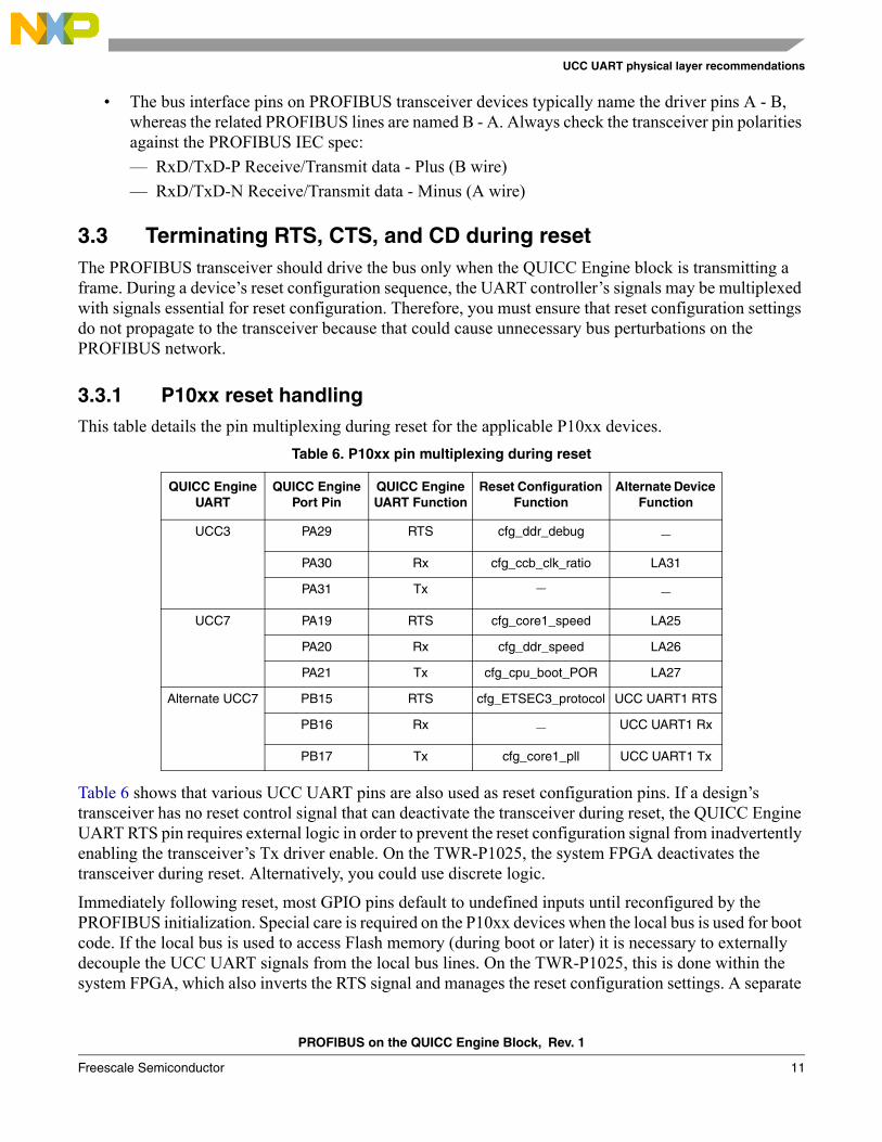
3.3.1 P10xx reset handlingThis table details the pin multiplexing during reset for the applicable P10xx devices.
Table 6 shows that various UCC UART pins are also used as reset configuration pins. If a design’s transceiver has no reset control signal that can deactivate the transceiver during reset, the QUICC Engine UART RTS pin requires external logic in order to prevent the reset configuration signal from inadvertently enabling the transceiver’s Tx driver enable. On the TWR-P1025, the system FPGA deactivates the transceiver during reset. Alternatively, you could use discrete logic.
Immediately following reset, most GPIO pins default to undefined inputs until reconfigured by the PROFIBUS initialization. Special care is required on the P10xx devices when the local bus is used for boot code. If the local bus is used to access Flash memory (during boot or later) it is necessary to externally decouple the UCC UART signals from the local bus lines. On the TWR-P1025, this is done within the system FPGA, which also inverts the RTS signal and manages the reset configuration settings. A separate
Table 6. P10xx pin multiplexing during reset
QUICC Engine UART
QUICC Engine Port Pin
QUICC Engine UART Function
Reset Configuration Function
Alternate Device Function
UCC3 PA29 RTS cfg_ddr_debug –PA30 Rx cfg_ccb_clk_ratio LA31
PA31 Tx – –UCC7 PA19 RTS cfg_core1_speed LA25
PA20 Rx cfg_ddr_speed LA26
PA21 Tx cfg_cpu_boot_POR LA27
Alternate UCC7 PB15 RTS cfg_ETSEC3_protocol UCC UART1 RTS
PB16 Rx – UCC UART1 Rx
PB17 Tx cfg_core1_pll UCC UART1 Tx

PROFIBUS on the QUICC Engine Block, Rev. 1
12 Freescale Semiconductor
UCC UART physical layer recommendations
GPIO control line (PB29) is used to multiplex the UART signals under software control once the device has booted from the flash (on the local bus).
3.3.2 MPC830x reset handlingThis table details the pin multiplexing during reset for the applicable MPC830x devices.
Table 7 shows that various UCC UART pins are also used as reset configuration pins. See the description following Table 6 for information on handling RTS and transceiver enablement during reset.
3.3.3 LS1020/21A reset handlingTable 8 details the pin multiplexing during reset.
Table 7. MPC830x pin multiplexing during reset
QUICC Engine UART
GPIO Port PinQUICC Engine UART Function
Reset Configuration Function
Alternate Device Function
UCC5 / HDLC2 GPIO18 Tx cfg_reset_source[2] TDM2_TD
GPIO19 Rx – TDM2_RD
GPIO20 CD – TDM2_TFS
GPIO21 CTS – TDM2_RFS
GPIO22 RTS cfg_reset_source[3] TDM2_STROBE
UCC7 / HDLC1 GPIO2 Tx cfg_reset_source[0] TDM1_TD
GPIO3 Rx – TDM1_RD
GPIO4 CD – TDM1_TFS
GPIO5 CTS – TDM1_RFS
GPIO6 RTS cfg_reset_source[1] TDM1_STROBE
Table 8. LS1020/21A pin multiplexing during reset
QUICC Engine UART
GPIO port pinQUICC Engine UART function
Reset configuration function
UCC1 / TDMA gpio_4[11] Tx –gpio_4[9] Rx –
gpio_4[13] CD –gpio_4[10] CTS –gpio_412] RTS –

PROFIBUS on the QUICC Engine Block, Rev. 1
Freescale Semiconductor 13
UCC UART physical layer recommendations
Table 8 shows that the UCC UART pins are not multiplexed with reset configuration pins. However during reset the user must ensure that the RTS signal disables the transceiver to avoid bus perturbations on the PROFIBUS network. Alternatively the user can ensure that the transceiver is disabled during reset.
3.4 Enabling and disabling a portThe QUICC Engine UCC emits a one-character-wide pulse (11 bits) on the RTS signal when you write GUMR_L[ENT] = 1. This occurs when enabling after device PORESET and every time thereafter when GUMR_L[ENT] transitions from 0 to 1.
It is imperative that this pulse does not propagate to the PROFIBUS physical layer and cause unnecessary bus perturbations. The transceiver must be decoupled from the RTS signal during the period where this pulse is present.
3.4.1 Mitigating the RTS pulse on P10xxBecause you can control the P10xx GPIO pins by programming each signal on an individual pin basis, configure the RTS and data pins after writing GUMR_L[ENT] = 1.
Alternatively, if the transceiver has a reset input, a GPIO line can control the RTS pulse by holding the transceiver in reset until GUMR_L[ENT] is set. If there is no transceiver reset input and no system FPGA, use external discrete logic controlled by a GPIO output to gate the UART signals.
3.4.2 Mitigating the RTS pulse on MPC830x and LS1020/21If the transceiver has a reset input, a GPIO line can control mitigation by holding the transceiver in reset until GUMR_L[ENT] is set. If there is no transceiver reset input and no system FPGA, use the external discrete logic controlled by a GPIO output to gate the UART signals.
UCC3 / TDMB gpio_4[16] Tx –gpio_4[14] Rx –gpio_4[18] CD –gpio_4[15] CTS –gpio_4[17] RTS –
Table 8. LS1020/21A pin multiplexing during reset
QUICC Engine UART
GPIO port pinQUICC Engine UART function
Reset configuration function
PROFIBUS on the QUICC Engine Block, Rev. 1
14 Freescale Semiconductor
Enabling idle transmit mode
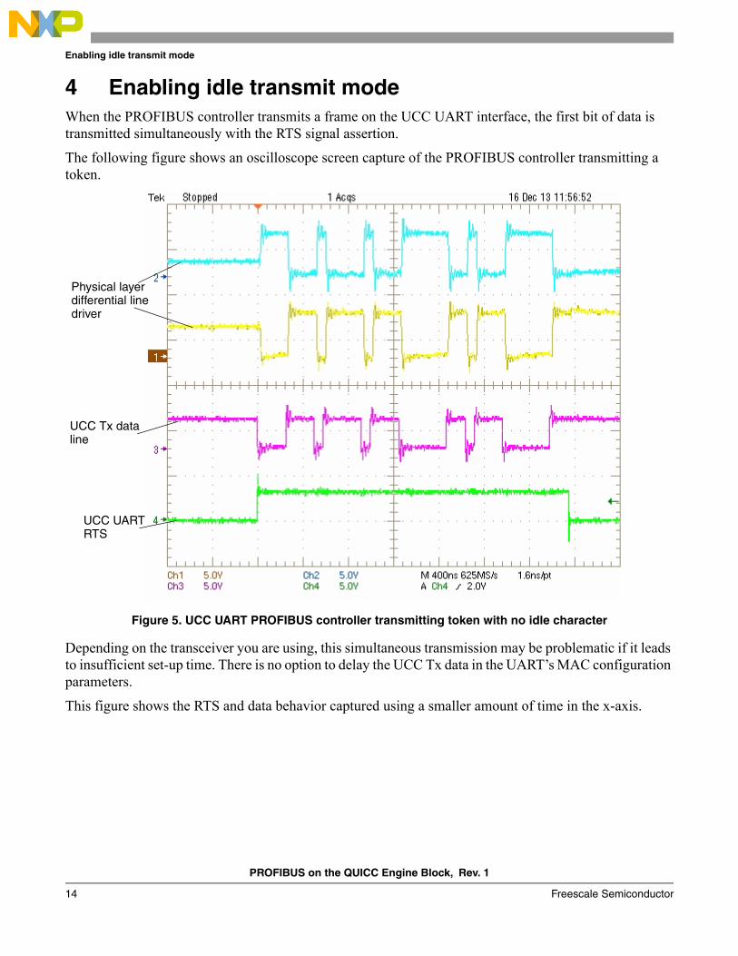
4 Enabling idle transmit modeWhen the PROFIBUS controller transmits a frame on the UCC UART interface, the first bit of data is transmitted simultaneously with the RTS signal assertion.
The following figure shows an oscilloscope screen capture of the PROFIBUS controller transmitting a token.
Figure 5. UCC UART PROFIBUS controller transmitting token with no idle character
Depending on the transceiver you are using, this simultaneous transmission may be problematic if it leads to insufficient set-up time. There is no option to delay the UCC Tx data in the UART’s MAC configuration parameters.
This figure shows the RTS and data behavior captured using a smaller amount of time in the x-axis.
Physical layer differential line driver
UCC UARTRTS
UCC Tx dataline

PROFIBUS on the QUICC Engine Block, Rev. 1
Freescale Semiconductor 15
Enabling idle transmit mode
Figure 6. UCC UART PROFIBUS controller transmitting token with no idle character (zoomed in)
As a workaround, the PROFIBUS microcode can be used in idle transmit mode. In this mode, an idle character is transmitted before the first data byte of the frame. This mode is useful for systems with slow transceivers or systems that cannot tolerate a lack of delay between RTS and data assertion.
This figure shows the RTS and data transmission behavior captured when the idle transmit mode is enabled.
UCC UARTRTS
UCC Tx dataline

PROFIBUS on the QUICC Engine Block, Rev. 1
16 Freescale Semiconductor
Enabling idle transmit mode
Figure 7. UCC UART PROFIBUS controller transmitting token with idle character
To enable the idle transmit mode, write profibus_mode[tx_idle] = 1.
To stay in the default mode (no delay), write profibus_mode[tx_idle] = 0.
The profibus_mode is a parameter located in the parameter of the PROFIBUS microcode. See the QEIWRM document for more information.
UCC UARTRTS
UCC Tx dataline
11 bits of logic = 1

PROFIBUS on the QUICC Engine Block, Rev. 1
Freescale Semiconductor 17
Memory resources
5 Memory resourcesEnsure that your configuration does not require more memory resources than are available. This is especially important regarding the MURAM.
This table details the MURAM sizes for the applicable P10xx, LS102x and MPC830x devices.
5.1 MURAM resources: single port slaveThis table details the amount of MURAM required for a UCC UART programmed for the PROFIBUS slave mode of operation.
The data highlights that a device with 16 k of MURAM cannot support a dual-port slave configuration if all SAPs use the full number of TxBDs and RxBDs. However, if the SAPs use fewer TxBDs and RxBDs (or if the configuration does not use all of the SAPs), a dual-port slave configuration is feasible.
Table 9. MURAM sizes
Device MURAM size (bytes)
P1012/P1021 24 k
P1016/P1025 24 k
MPC8306 16 k
MPC8309 16 k
LS1020/LS1021 24 k
Table 10. Slave parameter sizes in the MURAM 1
1 Values are based on the worst-case perspective.
Device MURAM size (bytes) Number required Total (bytes)
PROFIBUS parameter RAM
1024 1 1024
SAP tables 16 68 1088
Frame handling buffers 256 6 1536
SAP TxBD 8 4 21762
2 Number of SAP tables * Number of SAP TxBDs * Size of SAP TxBD
SAP RxBD 8 4 21763
3 Number of SAP tables * Number of SAP RxBDs * Size of SAP RxBD
Tx interrupt queue entry 2 32 64
Rx interrupt queue entry 2 32 64
LSAP_TxBDs 8 65 520
Combined Total (Bytes) 8648
PROFIBUS on the QUICC Engine Block, Rev. 1
18 Freescale Semiconductor
Memory resources
NOTE
This analysis does not take into account parameter alignment (see the QEIWRM PROFIBUS chapter for more information). This analysis simply highlights that MURAM availability may become an issue depending on the configuration.
Recommended best practice: Statically allocate the parameters in the MURAM, taking into account parameter alignment. The code should generate a warning message if the size of the allocated memory overshoots half the device’s MURAM size.
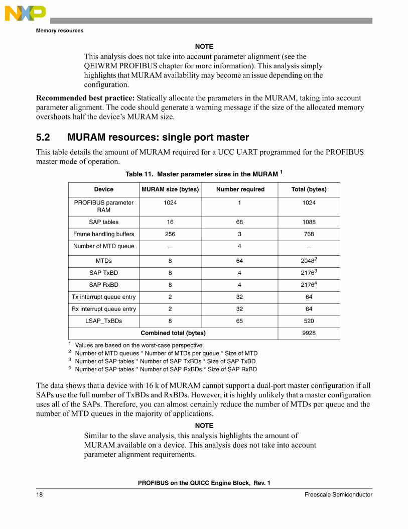
5.2 MURAM resources: single port masterThis table details the amount of MURAM required for a UCC UART programmed for the PROFIBUS master mode of operation.
The data shows that a device with 16 k of MURAM cannot support a dual-port master configuration if all SAPs use the full number of TxBDs and RxBDs. However, it is highly unlikely that a master configuration uses all of the SAPs. Therefore, you can almost certainly reduce the number of MTDs per queue and the number of MTD queues in the majority of applications.
NOTE
Similar to the slave analysis, this analysis highlights the amount of MURAM available on a device. This analysis does not take into account parameter alignment requirements.
Table 11. Master parameter sizes in the MURAM 1
1 Values are based on the worst-case perspective.
Device MURAM size (bytes) Number required Total (bytes)
PROFIBUS parameter RAM
1024 1 1024
SAP tables 16 68 1088
Frame handling buffers 256 3 768
Number of MTD queue – 4 –MTDs 8 64 20482
2 Number of MTD queues * Number of MTDs per queue * Size of MTD
SAP TxBD 8 4 21763
3 Number of SAP tables * Number of SAP TxBDs * Size of SAP TxBD
SAP RxBD 8 4 21764
4 Number of SAP tables * Number of SAP RxBDs * Size of SAP RxBD
Tx interrupt queue entry 2 32 64
Rx interrupt queue entry 2 32 64
LSAP_TxBDs 8 65 520
Combined total (bytes) 9928

PROFIBUS on the QUICC Engine Block, Rev. 1
Freescale Semiconductor 19
TWR-P1025 disclaimer
Recommended best practice: Statically allocate the parameters in the MURAM, taking into account parameter alignment. The code should generate a warning message if the size of the allocated memory overshoots half the device’s MURAM size.
6 TWR-P1025 disclaimerThe TWR-P1025 and P1025 devices are not recommended for PROFIBUS. See Table 2 for specific clock and frequency values.
In summary:• Given the maximum specified QE clock, commonly used baud rates cannot be derived.• The CCB clock is not a multiple of the baud rates. As a result, PROFIBUS IEC timers cannot be
calculated accurately.
Recommended best practice: Use the TWR-P1025 and P1025 devices for PROFIBUS evaluation purposes only.
It is possible to run this device out of spec to achieve a 384 MHz QUICC Engine block and baud rates up to 12 MHz. To do this, Freescale development engineers use the following parameters:
• 64 MHz SYSCLK• CCB Clock: SYSCLK Ratio = 6:1, yielding CCB and QE clock equal to 384 MHz• e500 core: CCB clock ratio = 1:1, yielding a core frequency of 384 MHz• DDR complex: DDRCLK ratio = 10:1, the DDRCLK is 66.667 MHz thus yielding a 666.67 MHz
DDR frequency
WARNINGThese operating parameters have proven to be stable during development and testing by Freescale. Because the device is out of specification regarding the QUICC Engine frequency, Freescale cannot make any guarantees about its operability in all evaluation scenarios.
PROFIBUS on the QUICC Engine Block, Rev. 1
20 Freescale Semiconductor
GPIO configuration example code
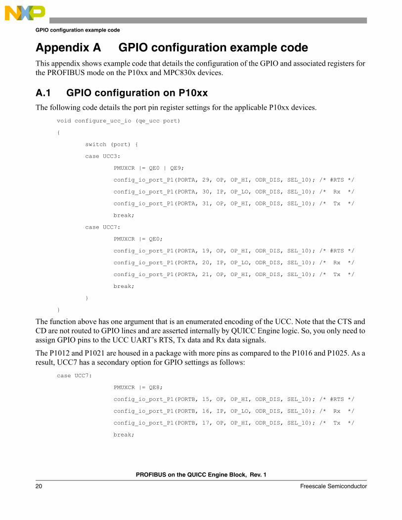
Appendix A GPIO configuration example codeThis appendix shows example code that details the configuration of the GPIO and associated registers for the PROFIBUS mode on the P10xx and MPC830x devices.
A.1 GPIO configuration on P10xxThe following code details the port pin register settings for the applicable P10xx devices.
void configure_ucc_io (qe_ucc port)
{
switch (port) {
case UCC3:
PMUXCR |= QE0 | QE9;
config_io_port_P1(PORTA, 29, OP, OP_HI, ODR_DIS, SEL_10); /* #RTS */
config_io_port_P1(PORTA, 30, IP, OP_LO, ODR_DIS, SEL_10); /* Rx */
config_io_port_P1(PORTA, 31, OP, OP_HI, ODR_DIS, SEL_10); /* Tx */
break;
case UCC7:
PMUXCR |= QE0;
config_io_port_P1(PORTA, 19, OP, OP_HI, ODR_DIS, SEL_10); /* #RTS */
config_io_port_P1(PORTA, 20, IP, OP_LO, ODR_DIS, SEL_10); /* Rx */
config_io_port_P1(PORTA, 21, OP, OP_HI, ODR_DIS, SEL_10); /* Tx */
break;
}
}
The function above has one argument that is an enumerated encoding of the UCC. Note that the CTS and CD are not routed to GPIO lines and are asserted internally by QUICC Engine logic. So, you only need to assign GPIO pins to the UCC UART’s RTS, Tx data and Rx data signals.
The P1012 and P1021 are housed in a package with more pins as compared to the P1016 and P1025. As a result, UCC7 has a secondary option for GPIO settings as follows:
case UCC7:
PMUXCR |= QE8;
config_io_port_P1(PORTB, 15, OP, OP_HI, ODR_DIS, SEL_10); /* #RTS */
config_io_port_P1(PORTB, 16, IP, OP_LO, ODR_DIS, SEL_10); /* Rx */
config_io_port_P1(PORTB, 17, OP, OP_HI, ODR_DIS, SEL_10); /* Tx */
break;
PROFIBUS on the QUICC Engine Block, Rev. 1
Freescale Semiconductor 21
GPIO configuration example code
A.2 GPIO configuration on MPC830xThe following code details the port pin register settings for the MPC8306 device.
case UCC5: /* HDLC2 */
/* CD= GPIO20, CTS= GPIO21, RTS= GPIO22, RX= GPIO19, TX= GPIO18 */
GPR_1 |= GPIO_16_22_SEL;
SICR_2 &= ~(BIT14 | BIT15); /* SICR_2::HDLC2_A => HDLC2 (UART) lines */
break;
case UCC7: /* HDLC1 */
/* CD= GPIO04, CTS= GPIO05, RTS= GPIO06, RX= GPIO03, TX= GPIO02 */
GPR_1 |= GPIO_0_6_SEL;
SICR_1 |= BIT31; /* SICR_1::HDLC1_A => GPIO3 => Rx line */
SICR_1 &= ~BIT30; /* SICR_1::HDLC1_A => GPIO3 => Rx line */
SICR_2 &= ~(BIT12 | BIT13); /* SICR_2::HDLC1_B => HDLC1 (UART) lines */
break;
The following code details the port pin register settings for the MPC8309 device.case UCC5: /* HDLC2 */
/* CD= GPIO20, CTS= GPIO21, RTS= GPIO22, RX= GPIO19, TX= GPIO18 */
GPR_1 |= GPIO_16_22_SEL;
SICR_2 &= ~(BIT8 | BIT9); /* SICR_2::HDLC2_A => HDLC2 (UART) lines */
break;
case UCC7: /* HDLC1 */
/* CD= GPIO04, CTS= GPIO05, RTS= GPIO06, RX= GPIO03, TX= GPIO02 */
GPR_1 |= GPIO_0_6_SEL;
SICR_2 &= ~(BIT2 | BIT3); /* SICR_2::HDLC1_B => HDLC1 (UART) lines */
break;
These devices have a group-wide programming hierarchy as compared to the pin-by-pin programming required on the P10xx devices. The user manuals for the MPC8306 and MPC8309 describes the UCC group as the HDLC port. The HDLC port settings are also relevant for UART mode. The UCC hardware register configuration determines the UCC mode of operation (UART or HDLC).
A.3 GPIO configuration on LS1020/21The LS1020/21 GPIO configuration occurs during reset configuration. The following RCW settings are required:
• UCC1 RCW QE_TDMA bits[427-429] = 0b010• UCC3 RCW QE_TDMB bits[430-432] = 0b010.

PROFIBUS on the QUICC Engine Block, Rev. 1
22 Freescale Semiconductor
GPIO configuration example code
These devices have a group-wide programming hierarchy as compared to the pin-by-pin programming required on the P10xx devices. The user manual for the LS1020/21 describes the UCC’s group as the HDLC or TDM interface. The HDLC UCC settings are also relevant for UART mode. The UCC hardware register configuration determines the UCC’s mode of operation (UART/HDLC or TDM). The RCW determines the mode of the pins connected to the UCC, either TDM or NMSI (use NMSI for UART/HDLC) based.
PROFIBUS on the QUICC Engine Block, Rev. 1
Freescale Semiconductor 23
GPIO configuration example code
Revision history This table describes the revision history for this application note.
Table 12. Document revision history
Rev Date Substantive Change(s)
1 12/2014 • Added LS1021A and LS1021A as relevant devices. • Updated section, 1.2, “Internally sourcing BRG clocks.” • Added 288 MHz as a recommended operating frequency. • Added new section, 1.4, “Configuration for recommended operating frequencies.” • Added new section, 3.3.3, “LS1020/21A reset handling.” • Added new appendix, A.3, “GPIO configuration on LS1020/21.”
0 03/2014 Initial release
Document Number: AN4877Rev. 1
12/2014
Information in this document is provided solely to enable system and software
implementers to use Freescale products. There are no express or implied copyright
licenses granted hereunder to design or fabricate any integrated circuits based on the
information in this document.
Freescale reserves the right to make changes without further notice to any products
herein. Freescale makes no warranty, representation, or guarantee regarding the
suitability of its products for any particular purpose, nor does Freescale assume any
liability arising out of the application or use of any product or circuit, and specifically
disclaims any and all liability, including without limitation consequential or incidental
damages. “Typical” parameters that may be provided in Freescale data sheets and/or
specifications can and do vary in different applications, and actual performance may vary
over time. All operating parameters, including “typicals,” must be validated for each
customer application by customer’s technical experts. Freescale does not convey any
license under its patent rights nor the rights of others. Freescale sells products pursuant
to standard terms and conditions of sale, which can be found at the following address:
freescale.com/SalesTermsandConditions.
How to Reach Us:
Home Page: freescale.com
Web Support: freescale.com/support
Freescale, the Freescale logo, PowerQUICC, and QorIQ are trademarks of Freescale
Semiconductor, Inc., Reg. U.S. Pat. & Tm. Off. QUICC Engine is a trademark of
Freescale Semiconductor, Inc. All other product or service names are the property of
their respective owners. The Power Architecture and Power.org word marks and the
Power and Power.org logos and related marks are trademarks and service marks
licensed by Power.org.
© 2014 Freescale Semiconductor, Inc.