
AN45 - Measurement and Control Circuit Collection · smoothly. The two of us had mastered feedings,...
24
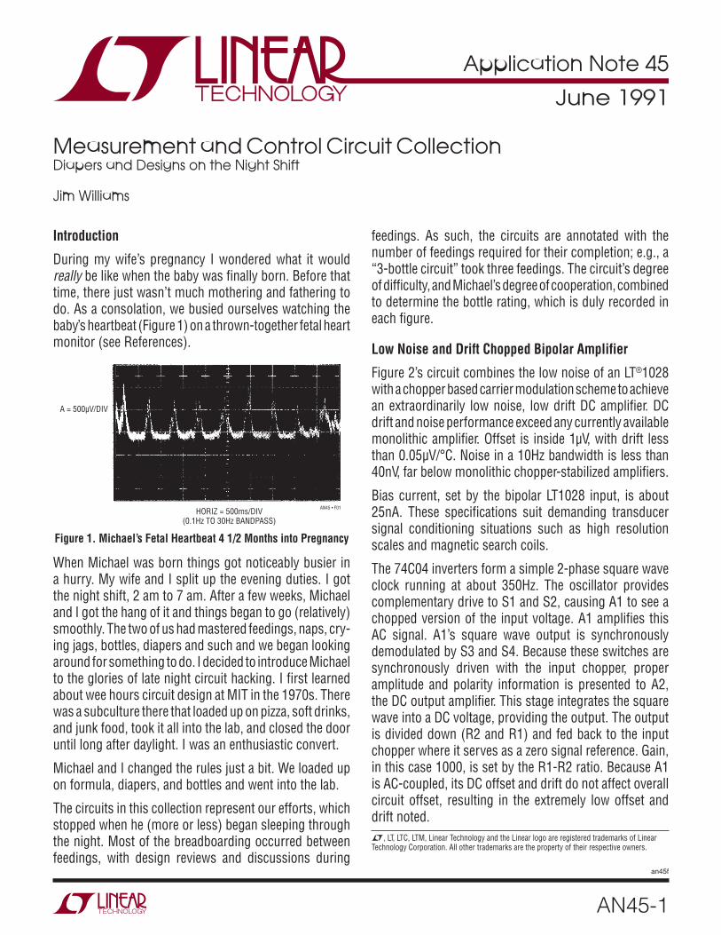
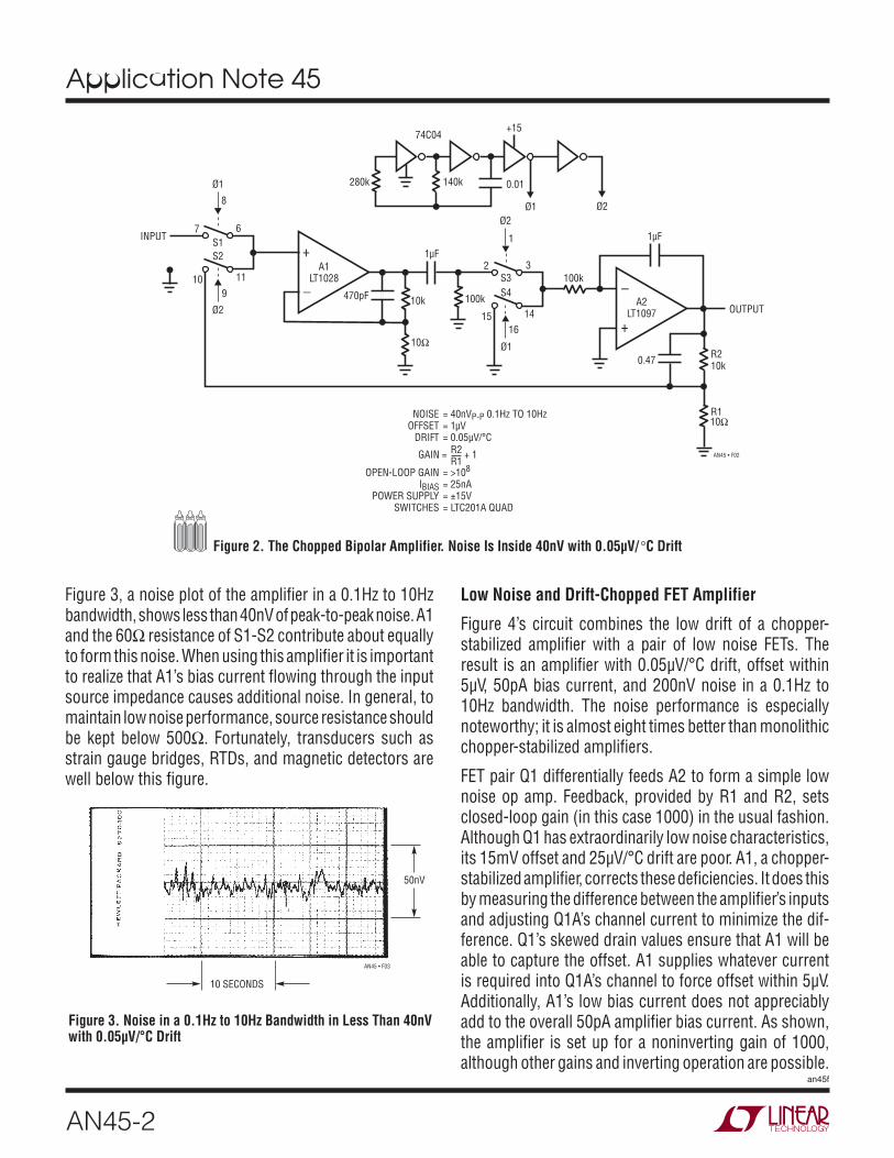
Application Note 45 AN45-1 an45f June 1991 Measurement and Control Circuit Collection Diapers and Designs on the Night Shift Jim Williams L, LT, LTC, LTM, Linear Technology and the Linear logo are registered trademarks of Linear Technology Corporation. All other trademarks are the property of their respective owners. Introduction During my wife’s pregnancy I wondered what it would really be like when the baby was finally born. Before that time, there just wasn’t much mothering and fathering to do. As a consolation, we busied ourselves watching the baby’s heartbeat (Figure 1) on a thrown-together fetal heart monitor (see References). Figure 1. Michael’s Fetal Heartbeat 4 1/2 Months into Pregnancy HORIZ = 500ms/DIV (0.1Hz TO 30Hz BANDPASS) A = 500μV/DIV When Michael was born things got noticeably busier in a hurry. My wife and I split up the evening duties. I got the night shift, 2 am to 7 am. After a few weeks, Michael and I got the hang of it and things began to go (relatively) smoothly. The two of us had mastered feedings, naps, cry- ing jags, bottles, diapers and such and we began looking around for something to do. I decided to introduce Michael to the glories of late night circuit hacking. I first learned about wee hours circuit design at MIT in the 1970s. There was a subculture there that loaded up on pizza, soft drinks, and junk food, took it all into the lab, and closed the door until long after daylight. I was an enthusiastic convert. Michael and I changed the rules just a bit. We loaded up on formula, diapers, and bottles and went into the lab. The circuits in this collection represent our efforts, which stopped when he (more or less) began sleeping through the night. Most of the breadboarding occurred between feedings, with design reviews and discussions during feedings. As such, the circuits are annotated with the number of feedings required for their completion; e.g., a “3-bottle circuit” took three feedings. The circuit’s degree of difficulty, and Michael’s degree of cooperation, combined to determine the bottle rating, which is duly recorded in each figure. Low Noise and Drift Chopped Bipolar Amplifier Figure 2’s circuit combines the low noise of an LT ® 1028 with a chopper based carrier modulation scheme to achieve an extraordinarily low noise, low drift DC amplifier. DC drift and noise performance exceed any currently available monolithic amplifier. Offset is inside 1μV, with drift less than 0.05μV/°C. Noise in a 10Hz bandwidth is less than 40nV, far below monolithic chopper-stabilized amplifiers. Bias current, set by the bipolar LT1028 input, is about 25nA. These specifications suit demanding transducer signal conditioning situations such as high resolution scales and magnetic search coils. The 74C04 inverters form a simple 2-phase square wave clock running at about 350Hz. The oscillator provides complementary drive to S1 and S2, causing A1 to see a chopped version of the input voltage. A1 amplifies this AC signal. A1’s square wave output is synchronously demodulated by S3 and S4. Because these switches are synchronously driven with the input chopper, proper amplitude and polarity information is presented to A2, the DC output amplifier. This stage integrates the square wave into a DC voltage, providing the output. The output is divided down (R2 and R1) and fed back to the input chopper where it serves as a zero signal reference. Gain, in this case 1000, is set by the R1-R2 ratio. Because A1 is AC-coupled, its DC offset and drift do not affect overall circuit offset, resulting in the extremely low offset and drift noted.
Transcript of AN45 - Measurement and Control Circuit Collection · smoothly. The two of us had mastered feedings,...
Application Note 45
AN45-1
an45f
June 1991
Measurement and Control Circuit CollectionDiapers and Designs on the Night Shift
Jim Williams
L, LT, LTC, LTM, Linear Technology and the Linear logo are registered trademarks of Linear Technology Corporation. All other trademarks are the property of their respective owners.
Introduction
During my wife’s pregnancy I wondered what it would really be like when the baby was finally born. Before that time, there just wasn’t much mothering and fathering to do. As a consolation, we busied ourselves watching the baby’s heartbeat (Figure 1) on a thrown-together fetal heart monitor (see References).
Figure 1. Michael’s Fetal Heartbeat 4 1/2 Months into Pregnancy
HORIZ = 500ms/DIV(0.1Hz TO 30Hz BANDPASS)
A = 500μV/DIV
When Michael was born things got noticeably busier in a hurry. My wife and I split up the evening duties. I got the night shift, 2 am to 7 am. After a few weeks, Michael and I got the hang of it and things began to go (relatively) smoothly. The two of us had mastered feedings, naps, cry-ing jags, bottles, diapers and such and we began looking around for something to do. I decided to introduce Michael to the glories of late night circuit hacking. I first learned about wee hours circuit design at MIT in the 1970s. There was a subculture there that loaded up on pizza, soft drinks, and junk food, took it all into the lab, and closed the door until long after daylight. I was an enthusiastic convert.
Michael and I changed the rules just a bit. We loaded up on formula, diapers, and bottles and went into the lab.
The circuits in this collection represent our efforts, which stopped when he (more or less) began sleeping through the night. Most of the breadboarding occurred between feedings, with design reviews and discussions during
feedings. As such, the circuits are annotated with the number of feedings required for their completion; e.g., a “3-bottle circuit” took three feedings. The circuit’s degree of difficulty, and Michael’s degree of cooperation, combined to determine the bottle rating, which is duly recorded in each figure.
Low Noise and Drift Chopped Bipolar Amplifier
Figure 2’s circuit combines the low noise of an LT®1028 with a chopper based carrier modulation scheme to achieve an extraordinarily low noise, low drift DC amplifier. DC drift and noise performance exceed any currently available monolithic amplifier. Offset is inside 1μV, with drift less than 0.05μV/°C. Noise in a 10Hz bandwidth is less than 40nV, far below monolithic chopper-stabilized amplifiers.
Bias current, set by the bipolar LT1028 input, is about 25nA. These specifications suit demanding transducer signal conditioning situations such as high resolution scales and magnetic search coils.
The 74C04 inverters form a simple 2-phase square wave clock running at about 350Hz. The oscillator provides complementary drive to S1 and S2, causing A1 to see a chopped version of the input voltage. A1 amplifies this AC signal. A1’s square wave output is synchronously demodulated by S3 and S4. Because these switches are synchronously driven with the input chopper, proper amplitude and polarity information is presented to A2, the DC output amplifier. This stage integrates the square wave into a DC voltage, providing the output. The output is divided down (R2 and R1) and fed back to the input chopper where it serves as a zero signal reference. Gain, in this case 1000, is set by the R1-R2 ratio. Because A1 is AC-coupled, its DC offset and drift do not affect overall circuit offset, resulting in the extremely low offset and drift noted.
Application Note 45
AN45-2
an45f
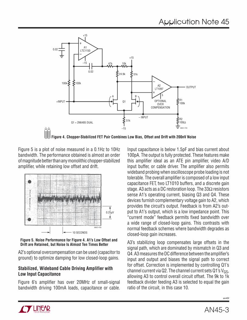
Figure 3, a noise plot of the amplifier in a 0.1Hz to 10Hz bandwidth, shows less than 40nV of peak-to-peak noise. A1 and the 60Ω resistance of S1-S2 contribute about equally to form this noise. When using this amplifier it is important to realize that A1’s bias current flowing through the input source impedance causes additional noise. In general, to maintain low noise performance, source resistance should be kept below 500Ω. Fortunately, transducers such as strain gauge bridges, RTDs, and magnetic detectors are well below this figure.
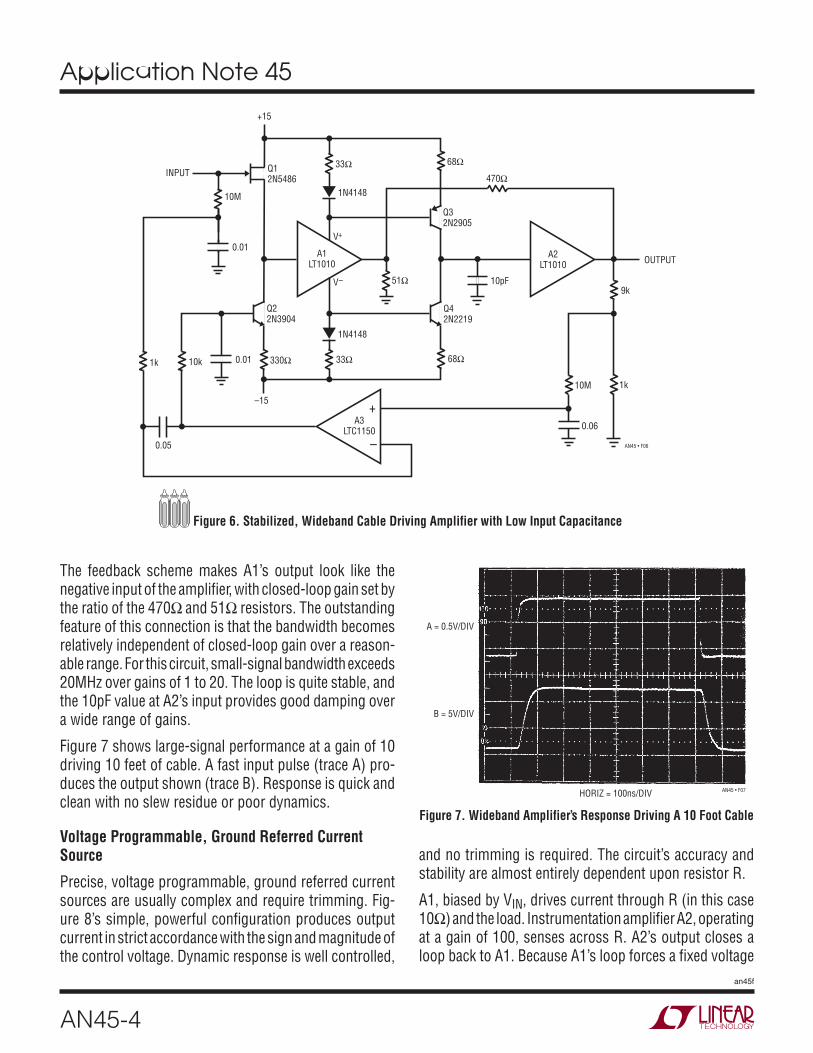
Low Noise and Drift-Chopped FET Amplifier
Figure 4’s circuit combines the low drift of a chopper-stabilized amplifier with a pair of low noise FETs. The result is an amplifier with 0.05μV/°C drift, offset within 5μV, 50pA bias current, and 200nV noise in a 0.1Hz to 10Hz bandwidth. The noise performance is especially noteworthy; it is almost eight times better than monolithic chopper-stabilized amplifiers.
FET pair Q1 differentially feeds A2 to form a simple low noise op amp. Feedback, provided by R1 and R2, sets closed-loop gain (in this case 1000) in the usual fashion. Although Q1 has extraordinarily low noise characteristics, its 15mV offset and 25μV/°C drift are poor. A1, a chopper-stabilized amplifier, corrects these deficiencies. It does this by measuring the difference between the amplifier’s inputs and adjusting Q1A’s channel current to minimize the dif-ference. Q1’s skewed drain values ensure that A1 will be able to capture the offset. A1 supplies whatever current is required into Q1A’s channel to force offset within 5μV. Additionally, A1’s low bias current does not appreciably add to the overall 50pA amplifier bias current. As shown, the amplifier is set up for a noninverting gain of 1000, although other gains and inverting operation are possible.
+
–
Ω
+15
Ø1
Ø1
141516
3
1
S4S3
OUTPUT
_
+A1
Ø1
INPUT7
11
S16
GAIN =
R1NOISE
OPEN-LOOP GAINIBIAS
POWER SUPPLYSWITCHES
P-P
R1+ 1
Figure 2. The Chopped Bipolar Amplifier. Noise Is Inside 40nV with 0.05μV/ °C Drift
10 SECONDS
50nV
Figure 3. Noise in a 0.1Hz to 10Hz Bandwidth in Less Than 40nV with 0.05μV/°C Drift
Application Note 45
AN45-3
an45f
Figure 5 is a plot of noise measured in a 0.1Hz to 10Hz bandwidth. The performance obtained is almost an order of magnitude better than any monolithic chopper-stabilized amplifier, while retaining low offset and drift.
Input capacitance is below 1.5pF and bias current about 100pA. The output is fully protected. These features make this amplifier ideal as an ATE pin amplifier, video A/D input buffer, or cable driver. The amplifier also permits wideband probing when oscilloscope probe loading is not tolerable. The overall amplifier is composed of a low input capacitance FET, two LT1010 buffers, and a discrete gain stage. A3 acts as a DC restoration loop. The 33Ω resistors sense A1’s operating current, biasing Q3 and Q4. These devices furnish complementary voltage gain to A2, which provides the circuit’s output. Feedback is from A2’s out-put to A1’s output, which is a low impedance point. This “current mode” feedback permits fixed bandwidth over a wide range of closed-loop gains. This contrasts with normal feedback schemes where bandwidth degrades as closed-loop gain increases.
A3’s stabilizing loop compensates large offsets in the signal path, which are dominated by mismatch in Q3 and Q4. A3 measures the DC difference between the amplifier’s input and output and biases the signal path to correct for offset. Correction is implemented by controlling Q1’s channel current via Q2. The channel current sets Q1’s VGS, allowing A3 to control overall circuit offset. The 9k to 1k feedback divider feeding A3 is selected to equal the gain ratio of the circuit, in this case 10.
+
–
R1
R2
+
–
+15
+15
–15
–15
A1
A B
A2
OPTIONALOVER
COMPENSATION
OUTPUT
– INPUT
Q1
5
+INPUT
Q1 = 2N6485 DUAL
Figure 4. Chopper-Stabilized FET Pair Combines Low Bias, Offset and Drift with 200nV Noise
Figure 5. Noise Performance for Figure 4. A1’s Low Offset and Drift are Retained, but Noise Is Almost Ten Times Better
10 SECONDS
0.25μV
A2’s optional overcompensation can be used (capacitor to ground) to optimize damping for low closed-loop gains.
Stabilized, Wideband Cable Driving Amplifier with Low Input Capacitance
Figure 6’s amplifier has over 20MHz of small-signal bandwidth driving 100mA loads, capacitance or cable.
Application Note 45
AN45-4
an45f
The feedback scheme makes A1’s output look like the negative input of the amplifier, with closed-loop gain set by the ratio of the 470Ω and 51Ω resistors. The outstanding feature of this connection is that the bandwidth becomes relatively independent of closed-loop gain over a reason-able range. For this circuit, small-signal bandwidth exceeds 20MHz over gains of 1 to 20. The loop is quite stable, and the 10pF value at A2’s input provides good damping over a wide range of gains.
Figure 7 shows large-signal performance at a gain of 10 driving 10 feet of cable. A fast input pulse (trace A) pro-duces the output shown (trace B). Response is quick and clean with no slew residue or poor dynamics.
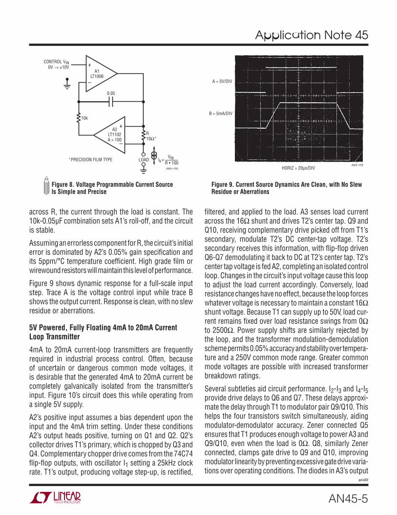
Voltage Programmable, Ground Referred Current Source
Precise, voltage programmable, ground referred current sources are usually complex and require trimming. Fig-ure 8’s simple, powerful configuration produces output current in strict accordance with the sign and magnitude of the control voltage. Dynamic response is well controlled,
and no trimming is required. The circuit’s accuracy and stability are almost entirely dependent upon resistor R.
A1, biased by VIN, drives current through R (in this case 10Ω) and the load. Instrumentation amplifier A2, operating at a gain of 100, senses across R. A2’s output closes a loop back to A1. Because A1’s loop forces a fixed voltage
A2A1
9k
1k
OUTPUT
Q2
INPUT
Q42N2219
+15
Q3
A3
1k
+
–
–15
Q1
V+
V–
Figure 6. Stabilized, Wideband Cable Driving Amplifier with Low Input Capacitance
HORIZ = 100ns/DIV
B = 5V/DIV
A = 0.5V/DIV
Figure 7. Wideband Amplifier’s Response Driving A 10 Foot Cable
Application Note 45
AN45-5
an45f
across R, the current through the load is constant. The 10k-0.05μF combination sets A1’s roll-off, and the circuit is stable.
Assuming an errorless component for R, the circuit’s initial error is dominated by A2’s 0.05% gain specification and its 5ppm/°C temperature coefficient. High grade film or wirewound resistors will maintain this level of performance.
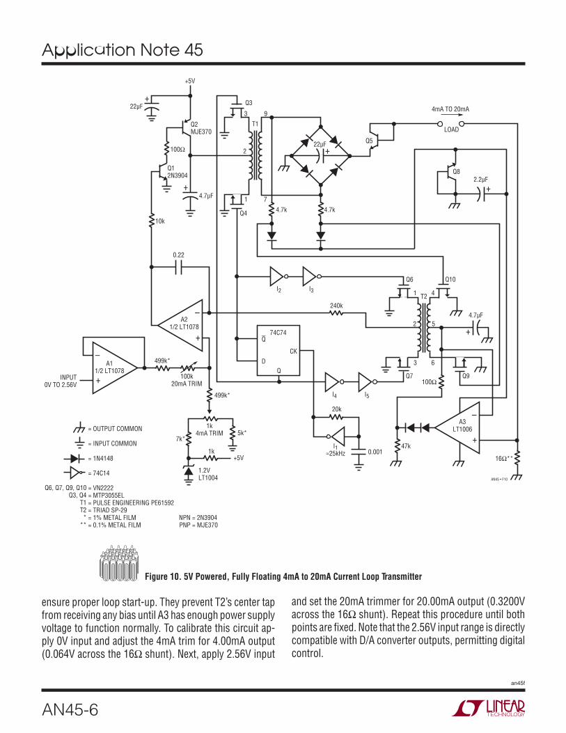
Figure 9 shows dynamic response for a full-scale input step. Trace A is the voltage control input while trace B shows the output current. Response is clean, with no slew residue or aberrations.
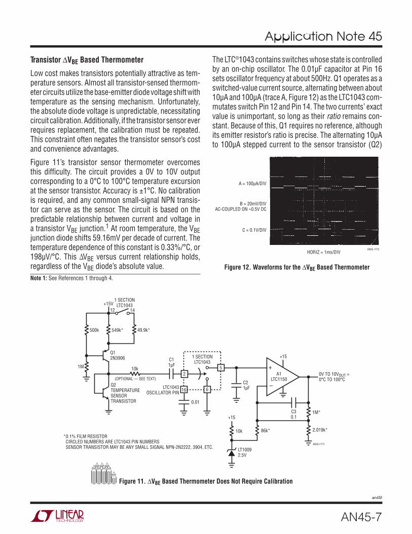
5V Powered, Fully Floating 4mA to 20mA Current Loop Transmitter
4mA to 20mA current-loop transmitters are frequently required in industrial process control. Often, because of uncertain or dangerous common mode voltages, it is desirable that the generated 4mA to 20mA current be completely galvanically isolated from the transmitter’s input. Figure 10’s circuit does this while operating from a single 5V supply.
A2’s positive input assumes a bias dependent upon the input and the 4mA trim setting. Under these conditions A2’s output heads positive, turning on Q1 and Q2. Q2’s collector drives T1’s primary, which is chopped by Q3 and Q4. Complementary chopper drive comes from the 74C74 flip-flop outputs, with oscillator I1 setting a 25kHz clock rate. T1’s output, producing voltage step-up, is rectified,
filtered, and applied to the load. A3 senses load current across the 16Ω shunt and drives T2’s center tap. Q9 and Q10, receiving complementary drive picked off from T1’s secondary, modulate T2’s DC center-tap voltage. T2’s secondary receives this information, with flip-flop driven Q6-Q7 demodulating it back to DC at T2’s center tap. T2’s center tap voltage is fed A2, completing an isolated control loop. Changes in the circuit’s input voltage cause this loop to adjust the load current accordingly. Conversely, load resistance changes have no effect, because the loop forces whatever voltage is necessary to maintain a constant 16Ω shunt voltage. Because T1 can supply up to 50V, load cur-rent remains fixed over load resistance swings from 0Ω to 2500Ω. Power supply shifts are similarly rejected by the loop, and the transformer modulation-demodulation scheme permits 0.05% accuracy and stability over tempera-ture and a 250V common mode range. Greater common mode voltages are possible with increased transformer breakdown ratings.
Several subtleties aid circuit performance. I2-I3 and I4-I5 provide drive delays to Q6 and Q7. These delays approxi-mate the delay through T1 to modulator pair Q9/Q10. This helps the four transistors switch simultaneously, aiding modulator-demodulator accuracy. Zener connected Q5 ensures that T1 produces enough voltage to power A3 and Q9/Q10, even when the load is 0Ω. Q8, similarly Zener connected, clamps gate drive to Q9 and Q10, improving modulator linearity by preventing excessive gate drive varia-tions over operating conditions. The diodes in A3’s output
+
–
+
–
R
A1
A2
=
HORIZ = 20μs/DIV
B = 5mA/DIV
A = 5V/DIV
Figure 8. Voltage Programmable Current Source Is Simple and Precise
Figure 9. Current Source Dynamics Are Clean, with No Slew Residue or Aberrations
Application Note 45
AN45-6
an45f
ensure proper loop start-up. They prevent T2’s center tap from receiving any bias until A3 has enough power supply voltage to function normally. To calibrate this circuit ap-ply 0V input and adjust the 4mA trim for 4.00mA output (0.064V across the 16Ω shunt). Next, apply 2.56V input
and set the 20mA trimmer for 20.00mA output (0.3200V across the 16Ω shunt). Repeat this procedure until both points are fixed. Note that the 2.56V input range is directly compatible with D/A converter outputs, permitting digital control.
4.7k4.7k
Q3
3 9
2
7
Q4
+5V
A2
–
+
+
–
INPUT
499k*
+5V
5k*7k*
499k*
74C74Q
DQ
CK
I≈25kHz
I4 I5
I2 I3
Q7 Q9
3
2
4T2
5
A3–
+47k
= VN2222
T2*
**
Q5
NPNPNP
Q2
+
+ +
+
+Figure 10. 5V Powered, Fully Floating 4mA to 20mA Current Loop Transmitter
Application Note 45
AN45-7
an45f
Transistor ∆VBE Based Thermometer
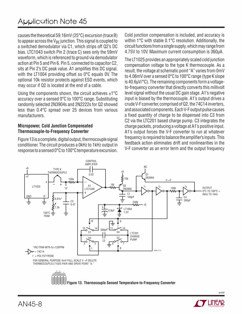
Low cost makes transistors potentially attractive as tem-perature sensors. Almost all transistor-sensed thermom-eter circuits utilize the base-emitter diode voltage shift with temperature as the sensing mechanism. Unfortunately, the absolute diode voltage is unpredictable, necessitating circuit calibration. Additionally, if the transistor sensor ever requires replacement, the calibration must be repeated. This constraint often negates the transistor sensor’s cost and convenience advantages.
Figure 11’s transistor sensor thermometer overcomes this difficulty. The circuit provides a 0V to 10V output corresponding to a 0°C to 100°C temperature excursion at the sensor transistor. Accuracy is ±1°C. No calibration is required, and any common small-signal NPN transis-tor can serve as the sensor. The circuit is based on the predictable relationship between current and voltage in a transistor VBE junction.1 At room temperature, the VBE junction diode shifts 59.16mV per decade of current. The temperature dependence of this constant is 0.33%/°C, or 198μV/°C. This ΔVBE versus current relationship holds, regardless of the VBE diode’s absolute value.
The LTC®1043 contains switches whose state is controlled by an on-chip oscillator. The 0.01μF capacitor at Pin 16 sets oscillator frequency at about 500Hz. Q1 operates as a switched-value current source, alternating between about 10μA and 100μA (trace A, Figure 12) as the LTC1043 com-mutates switch Pin 12 and Pin 14. The two currents’ exact value is unimportant, so long as their ratio remains con-stant. Because of this, Q1 requires no reference, although its emitter resistor’s ratio is precise. The alternating 10μA to 100μA stepped current to the sensor transistor (Q2)
Note 1: See References 1 through 4.
+
–C2
=
C3
Q26
52
Figure 12. Waveforms for the ∆VBE Based Thermometer
Figure 11. ∆VBE Based Thermometer Does Not Require Calibration
HORIZ = 1ms/DIV
C = 0.1V/DIV
A = 100μA/DIV
AC-COUPLED ON ≈0.5V DC
Application Note 45
AN45-8
an45f
causes the theoretical 59.16mV (25°C) excursion (trace B) to appear across the VBE junction. This signal is coupled to a switched demodulator via C1, which strips off Q2’s DC bias. LTC1043 switch Pin 2 (trace C) sees only the 59mV waveform, which is referenced to ground via demodulator action at Pin 5 and Pin 6. Pin 5, connected to capacitor C2, sits at Pin 2’s DC peak value. A1 amplifies this DC signal, with the LT1004 providing offset so 0°C equals 0V. The optional 10k resistor protects against ESD events, which may occur if Q2 is located at the end of a cable.
Using the components shown, the circuit achieves ±1°C accuracy over a sensed 0°C to 100°C range. Substituting randomly selected 2N3904s and 2N2222s for Q2 showed less than 0.4°C spread over 25 devices from various manufacturers.
Micropower, Cold Junction Compensated Thermocouple-to-Frequency Converter
Figure 13 is a complete, digital output, thermocouple signal conditioner. The circuit produces a 0kHz to 1kHz output in response to a sensed 0°C to 100°C temperature excursion.
Cold junction compensation is included, and accuracy is within 1°C with stable 0.1°C resolution. Additionally, the circuit functions from a single supply, which may range from 4.75V to 10V. Maximum current consumption is 360μA.
The LT1025 provides an appropriately scaled cold junction compensation voltage to the type K thermocouple. As a result, the voltage at schematic point “A” varies from 0mV to 4.06mV over a sensed 0°C to 100°C range (type K slope is 40.6μV/°C). The remaining components form a voltage-to-frequency converter that directly converts this millivolt level signal without the usual DC gain stage. A1’s negative input is biased by the thermocouple. A1’s output drives a crude V-F converter, comprised of Q2, the 74C14 inverters, and associated components. Each V-F output pulse causes a fixed quantity of charge to be dispensed into C3 from C2 via the LTC201 based charge pump. C3 integrates the charge packets, producing a voltage at A1’s positive input. A1’s output forces the V-F converter to run at whatever frequency is required to balance the amplifier’s inputs. This feedback action eliminates drift and nonlinearities in the V-F converter as an error term and the output frequency
–+
–+–
+6
GND R
TRIM
“A”
CONTROL
†
6
8
S4
+6
I
NC
I I
C4
OUTPUT
V
PUMP
+6
†
+V
+
Figure 13. Thermocouple Sensed Temperature-to-Frequency Converter
Application Note 45
AN45-9
an45f
is solely a function of the DC conditions at A1’s inputs. The 0.02μF capacitor forms a dominant response pole at A1, stabilizing the loop. Chopper stabilized A1’s low VOS offset and drift eliminate offset error in the circuit, despite an output LSB value of only 4.06μV (0.1°C).
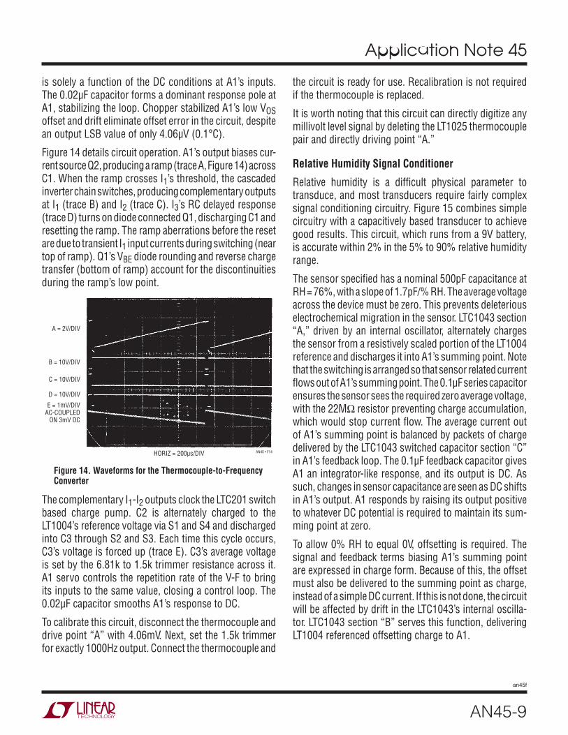
Figure 14 details circuit operation. A1’s output biases cur-rent source Q2, producing a ramp (trace A, Figure 14) across C1. When the ramp crosses I1’s threshold, the cascaded inverter chain switches, producing complementary outputs at I1 (trace B) and I2 (trace C). I3’s RC delayed response (trace D) turns on diode connected Q1, discharging C1 and resetting the ramp. The ramp aberrations before the reset are due to transient I1 input currents during switching (near top of ramp). Q1’s VBE diode rounding and reverse charge transfer (bottom of ramp) account for the discontinuities during the ramp’s low point.
the circuit is ready for use. Recalibration is not required if the thermocouple is replaced.
It is worth noting that this circuit can directly digitize any millivolt level signal by deleting the LT1025 thermocouple pair and directly driving point “A.”
Relative Humidity Signal Conditioner
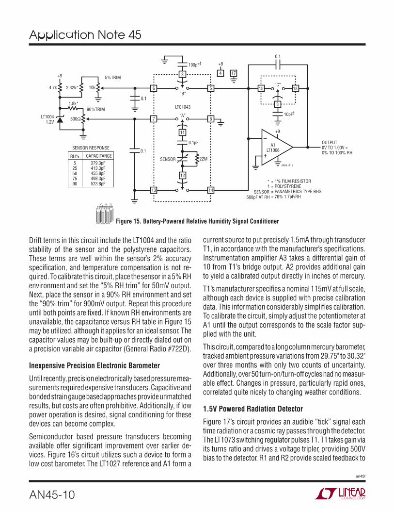
Relative humidity is a difficult physical parameter to transduce, and most transducers require fairly complex signal conditioning circuitry. Figure 15 combines simple circuitry with a capacitively based transducer to achieve good results. This circuit, which runs from a 9V battery, is accurate within 2% in the 5% to 90% relative humidity range.
The sensor specified has a nominal 500pF capacitance at RH = 76%, with a slope of 1.7pF/% RH. The average voltage across the device must be zero. This prevents deleterious electrochemical migration in the sensor. LTC1043 section “A,” driven by an internal oscillator, alternately charges the sensor from a resistively scaled portion of the LT1004 reference and discharges it into A1’s summing point. Note that the switching is arranged so that sensor related current flows out of A1’s summing point. The 0.1μF series capacitor ensures the sensor sees the required zero average voltage, with the 22MΩ resistor preventing charge accumulation, which would stop current flow. The average current out of A1’s summing point is balanced by packets of charge delivered by the LTC1043 switched capacitor section “C” in A1’s feedback loop. The 0.1μF feedback capacitor gives A1 an integrator-like response, and its output is DC. As such, changes in sensor capacitance are seen as DC shifts in A1’s output. A1 responds by raising its output positive to whatever DC potential is required to maintain its sum-ming point at zero.
To allow 0% RH to equal 0V, offsetting is required. The signal and feedback terms biasing A1’s summing point are expressed in charge form. Because of this, the offset must also be delivered to the summing point as charge, instead of a simple DC current. If this is not done, the circuit will be affected by drift in the LTC1043’s internal oscilla-tor. LTC1043 section “B” serves this function, delivering LT1004 referenced offsetting charge to A1.
Figure 14. Waveforms for the Thermocouple-to-Frequency Converter
HORIZ = 200μs/DIV
A = 2V/DIV
AC-COUPLED
The complementary I1-I2 outputs clock the LTC201 switch based charge pump. C2 is alternately charged to the LT1004’s reference voltage via S1 and S4 and discharged into C3 through S2 and S3. Each time this cycle occurs, C3’s voltage is forced up (trace E). C3’s average voltage is set by the 6.81k to 1.5k trimmer resistance across it. A1 servo controls the repetition rate of the V-F to bring its inputs to the same value, closing a control loop. The 0.02μF capacitor smooths A1’s response to DC.
To calibrate this circuit, disconnect the thermocouple and drive point “A” with 4.06mV. Next, set the 1.5k trimmer for exactly 1000Hz output. Connect the thermocouple and
Application Note 45
AN45-10
an45f
Drift terms in this circuit include the LT1004 and the ratio stability of the sensor and the polystyrene capacitors. These terms are well within the sensor’s 2% accuracy specification, and temperature compensation is not re-quired. To calibrate this circuit, place the sensor in a 5% RH environment and set the “5% RH trim” for 50mV output. Next, place the sensor in a 90% RH environment and set the “90% trim” for 900mV output. Repeat this procedure until both points are fixed. If known RH environments are unavailable, the capacitance versus RH table in Figure 15 may be utilized, although it applies for an ideal sensor. The capacitor values may be built-up or directly dialed out on a precision variable air capacitor (General Radio #722D).
Inexpensive Precision Electronic Barometer
Until recently, precision electronically based pressure mea-surements required expensive transducers. Capacitive and bonded strain gauge based approaches provide unmatched results, but costs are often prohibitive. Additionally, if low power operation is desired, signal conditioning for these devices can become complex.
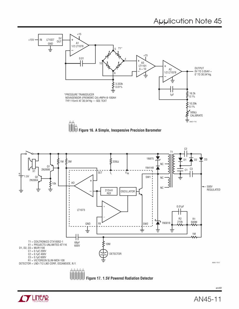
Semiconductor based pressure transducers becoming available offer significant improvement over earlier de-vices. Figure 16’s circuit utilizes such a device to form a low cost barometer. The LT1027 reference and A1 form a
current source to put precisely 1.5mA through transducer T1, in accordance with the manufacturer’s specifications. Instrumentation amplifier A3 takes a differential gain of 10 from T1’s bridge output. A2 provides additional gain to yield a calibrated output directly in inches of mercury.
T1’s manufacturer specifies a nominal 115mV at full scale, although each device is supplied with precise calibration data. This information considerably simplifies calibration. To calibrate the circuit, simply adjust the potentiometer at A1 until the output corresponds to the scale factor sup-plied with the unit.
This circuit, compared to a long column mercury barometer, tracked ambient pressure variations from 29.75" to 30.32" over three months with only two counts of uncertainty. Additionally, over 50 turn-on/turn-off cycles had no measur-able effect. Changes in pressure, particularly rapid ones, correlated quite nicely to changing weather conditions.
1.5V Powered Radiation Detector
Figure 17’s circuit provides an audible “tick” signal each time radiation or a cosmic ray passes through the detector. The LT1073 switching regulator pulses T1. T1 takes gain via its turns ratio and drives a voltage tripler, providing 500V bias to the detector. R1 and R2 provide scaled feedback to
+
–
4.7k
+9
“A”
“B”
4
+9
+9
“C”
OUTPUT
5
75
7
5
†
†
†
Figure 15. Battery-Powered Relative Humidity Signal Conditioner
Application Note 45
AN45-11
an45f
+
– 5
4 +
–+
–
5V
NC
NC
C1
D2
C2
C3
D3
68pF600V 10M
1N5818
DETECTOR
T1 =X1 =
D1, D2, D3 =C1 =C2 =C3 =R1 =
DETECTOR =
COILTRONICS CTX10052-1PROJECTS UNLIMITED AT11KMUR11000.1μF, 200V0.1μF, 400V0.1μF, 600VVICTOREEN SLIM-MOX-108LND-712 LND CORP., OCEANSIDE, N.Y.
1.5V
3M1M
10k
X1+
Q22N3904
Q12N3906
LT1073
AO
GND SW2FB
SET
SW1+
– 212mVREF.
OSCILLATOR
+
–
1N975
VIN
330Ω
IL
0.01μF
R1500M
1M
D1
500VREGULATED
1N4148NC
R2210k
T1
Figure 17. 1.5V Powered Radiation Detector
Figure 16. A Simple, Inexpensive Precision Barometer
Application Note 45
AN45-12
an45f
the LT1073, closing a control loop. The 0.01μF lag adds AC hysteresis and the Schottky diode clamps negative going T1 excursions. When radiation or a cosmic ray strikes the detector, impedance drops briefly, transferring a quick negative going spike through the 68pF capacitor. This spike triggers the LT1073’s auxiliary gain block, configured here as a comparator. Q1 and Q2 provide additional gain to drive the audible beeper. About 10 to 15 cosmic rays per minute are recorded in a normal environment.
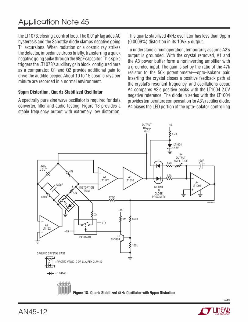
9ppm Distortion, Quartz Stabilized Oscillator
A spectrally pure sine wave oscillator is required for data converter, filter and audio testing. Figure 18 provides a stable frequency output with extremely low distortion.
This quartz stabilized 4kHz oscillator has less than 9ppm (0.0009%) distortion in its 10VP-P output.
To understand circuit operation, temporarily assume A2’s output is grounded. With the crystal removed, A1 and the A3 power buffer form a noninverting amplifier with a grounded input. The gain is set by the ratio of the 47k resistor to the 50k potentiometer—opto-isolator pair. Inserting the crystal closes a positive feedback path at the crystal’s resonant frequency, and oscillations occur. A4 compares A3’s positive peaks with the LT1004 2.5V negative reference. The diode in series with the LT1004 provides temperature compensation for A3’s rectifier diode. A4 biases the LED portion of the opto-isolator, controlling
–
+
+
–
47k
50k
DISTORTIONTRIM
560k
4kHzJ CUT
2k
A2
560k
–
+
470Ω
4.7k
+
–A4
4.7k
5kOUTPUT
MOUNTIN
PROXIMITY
A3
4.7k
2.5V
OUTPUTP-P
4kHz
2N3904
+
Figure 18. Quartz Stabilized 4kHz Oscillator with 9ppm Distortion
Application Note 45
AN45-13
an45f
the photoresistor’s resistance. This sets loop gain to a value permitting stable amplitude oscillations. The 10μF capacitor stabilizes this amplitude control loop.
A2’s function is to eliminate the common mode swing seen by A1. This dramatically reduces distortion due to A1’s common mode rejection limitations. A2 does this by servo controlling the 560kΩ-photocell junction to maintain its negative input at 0V. This action eliminates common mode swing at A1, leaving only the desired differential signal.
Q1 and the LTC201 switch form a start-up loop. When power is first applied oscillations may build very slowly. Under these conditions A4’s output saturates positive, turning on Q1. The LTC201 switch turns on, shunting the 2kΩ resistor across the 50kΩ potentiometer. This raises A1’s loop gain, forcing a rapid build-up of oscillations. When oscillations rise high enough A4 comes out of saturation, Q1 and the switch go off and the loop functions normally.
The circuit is adjusted for minimum distortion by adjust-ing the 50kΩ potentiometer while monitoring A3’s output with a distortion analyzer. This trim sets the voltage across the photocell to the optimum value for lowest distortion. The circuit’s power supply should be well regulated and bypassed to ensure the distortion figures quoted.
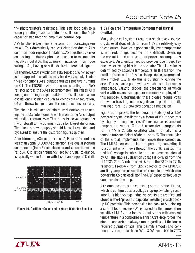
After trimming, A3’s output (trace A, Figure 19) contains less than 9ppm (0.0009%) distortion. Residual distortion components (trace B) include noise and second harmonic residue. Oscillation frequency, set by crystal tolerance, is typically within 50ppm with less than 2.5ppm/°C drift.
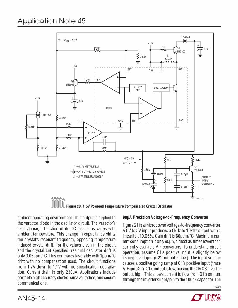
1.5V Powered Temperature Compensated Crystal Oscillator
Many single cell systems require a stable clock source. Crystal oscillators which run from 1.5V are relatively easy to construct. However, if good stability over temperature is required, things become more difficult. Ovenizing the crystal is one approach, but power consumption is excessive. An alternate method provides open loop, fre-quency correcting bias to the oscillator. The bias value is determined by absolute temperature. In this fashion, the oscillator’s thermal drift, which is repeatable, is corrected. The simplest way to do this is by slightly varying the crystal’s resonance point with a variable shunt or series impedance. Varactor diodes, the capacitance of which varies with reverse voltage, are commonly employed for this purpose. Unfortunately, these diodes require volts of reverse bias to generate significant capacitance shift, making direct 1.5V powered operation impossible.
Figure 20 improves the temperature stability of a 1.5V powered crystal oscillator by a factor of 20. It does this by slightly tuning the crystal’s resonance as ambient temperature varies. Q1 and associated components form a 1MHz Colpitts oscillator which normally has a temperature coefficient of about 1ppm/°C. The remainder of the circuit implements the temperature correction. The LM134 senses ambient temperature, converting it to a current which flows through the 30.1k resistor. This resistor’s voltage is subtracted from a reference potential by A1. The stable subtraction voltage is derived from the LT1073’s 212mV reference via Q2 and the 73.2k to 27.4k resistors. Feedback from Q2’s collector to the LT1073’s auxiliary amplifier closes the reference loop, which also powers the Colpitts oscillator. The 47μF capacitor frequency compensates the loop.
A1’s output controls the remaining portion of the LT1073, which is configured as a voltage step-up switching regu-lator. L1’s high voltage inductive events are rectified and stored in the 47μF output capacitor, resulting in a stepped-up DC potential. This potential is fed back to A1, closing a control loop. Because A1 is biased by the temperature sensitive LM134, the loop’s output varies with ambient temperature in a controlled manner. Q3’s drop forces the step-up converter to always run, regardless of the loop’s required output voltage. This permits smooth and con-tinuous varactor bias from 0V to 3.9V over a 0°C to 70°C
HORIZ = 100μs/DIV
DISTORTION
A = 5V/DIV
Figure 19. Oscillator Output and its 9ppm Distortion Residue
Application Note 45
AN45-14
an45f
ambient operating environment. This output is applied to the varactor diode in the oscillator circuit. The varactor’s capacitance, a function of its DC bias, thus varies with ambient temperature. This change in capacitance shifts the crystal’s resonant frequency, opposing temperature induced crystal drift. For the values given in the circuit and the crystal cut specified, residual oscillator drift is only 0.05ppm/°C. This compares favorably with 1ppm/°C drift with no compensation used. The circuit functions from 1.7V down to 1.1V with no specification degrada-tion. Current drain is only 230μA. Applications include portable high accuracy clocks, survival radios, and secure communications.
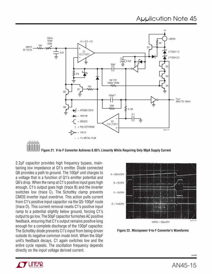
90μA Precision Voltage-to-Frequency Converter
Figure 21 is a micropower voltage-to-frequency converter. A 0V to 5V input produces a 0kHz to 10kHz output with a linearity of 0.05%. Gain drift is 80ppm/°C. Maximum cur-rent consumption is only 90μA, almost 30 times lower than currently available V-F converters. To understand circuit operation, assume C1’s positive input is slightly below its negative input (C2’s output is low). The input voltage causes a positive going ramp at C1’s positive input (trace A, Figure 22). C1’s output is low, biasing the CMOS inverter output high. This allows current to flow from Q1’s emitter, through the inverter supply pin to the 100pF capacitor. The
AO
GND
SET SW1IL
+
– OSCILLATOR
+
–
IN
L1
+
–A1
OUTPUT
Q1
L1
1N4148
+
+
Figure 20. 1.5V Powered Temperature Compensated Crystal Oscillator
Application Note 45
AN45-15
an45f
=
=
=
=
=
=
POLYSTYRENE
+
–
0V TO 5V
+
–
†
+V
Q4
f
†
Q7
Q6
Q5
+
Figure 21. V-to-F Converter Achieves 0.05% Linearity While Requiring Only 90μA Supply Current
Figure 22. Micropower V-to-F Converter's Waveforms
2.2μF capacitor provides high frequency bypass, main-taining low impedance at Q1’s emitter. Diode connected Q6 provides a path to ground. The 100pF unit charges to a voltage that is a function of Q1’s emitter potential and Q6’s drop. When the ramp at C1’s positive input goes high enough, C1’s output goes high (trace B) and the inverter switches low (trace C). The Schottky clamp prevents CMOS inverter input overdrive. This action pulls current from C1’s positive input capacitor via the Q5-100pF route (trace D). This current removal resets C1’s positive input ramp to a potential slightly below ground, forcing C1’s output to go low. The 50pF capacitor furnishes AC positive feedback, ensuring that C1’s output remains positive long enough for a complete discharge of the 100pF capacitor. The Schottky diode prevents C1’s input from being driven outside its negative common mode limit. When the 50pF unit’s feedback decays, C1 again switches low and the entire cycle repeats. The oscillation frequency depends directly on the input voltage derived current.
HORIZ = 20μs/DIV
D = 1mA/DIV
A = 50mV/DIV
B = 5V/DIV
C = 5V/DIV
Application Note 45
AN45-16
an45f
Q1’s emitter voltage must be carefully controlled to get low drive. Q3 and Q4 temperature compensate Q5 and Q6 while Q2 compensates Q1’s VBE. The two LT1034s are the actual voltage reference and the LM334 current source provides 35μA bias to the stack. The current drive provides excellent supply immunity (better than 40ppm/V) and also aids circuit temperature coefficient. It does this by utilizing the LM334’s 0.3%/°C temperature coefficient to slightly temperature modulate the voltage drop in the Q2-Q4 trio. This correction’s sign and magnitude directly oppose that of the –120ppm/°C, 100pF polystyrene capacitor, aiding overall circuit stability.
The Q1 emitter-follower efficiently delivers charge to the 100pF capacitor. Both base and collector current end up in the capacitor. The CMOS inverter provides low loss SPDT reference switching without significant drive losses. The 100pF capacitor draws only small transient currents during its charge and discharge cycles. The 50pF-47k positive feedback combination draws insignificantly small switch-ing currents. Figure 23, a plot of supply current versus operating frequency, reflects the low power design. At zero frequency, the LT1017’s quiescent current and the 35μA reference stack bias account for all current drain. There are no other paths for loss. As frequency scales up, the charge/discharge cycle of the 100pF capacitor introduces the 1.5μA/kHz increase shown.
2.7M-0.1μF lag, also goes high. This lifts C1’s negative input and grounds the positive input with Q7, initiating normal circuit action.
Because the charge pump is directly coupled to C1’s output, response is fast. The output settles within one cycle for a fast input step. To calibrate this circuit, apply 50mV and select the value at C1’s input for a 100Hz output. Then, apply 5V and trim the input potentiometer for a 10kHz output.
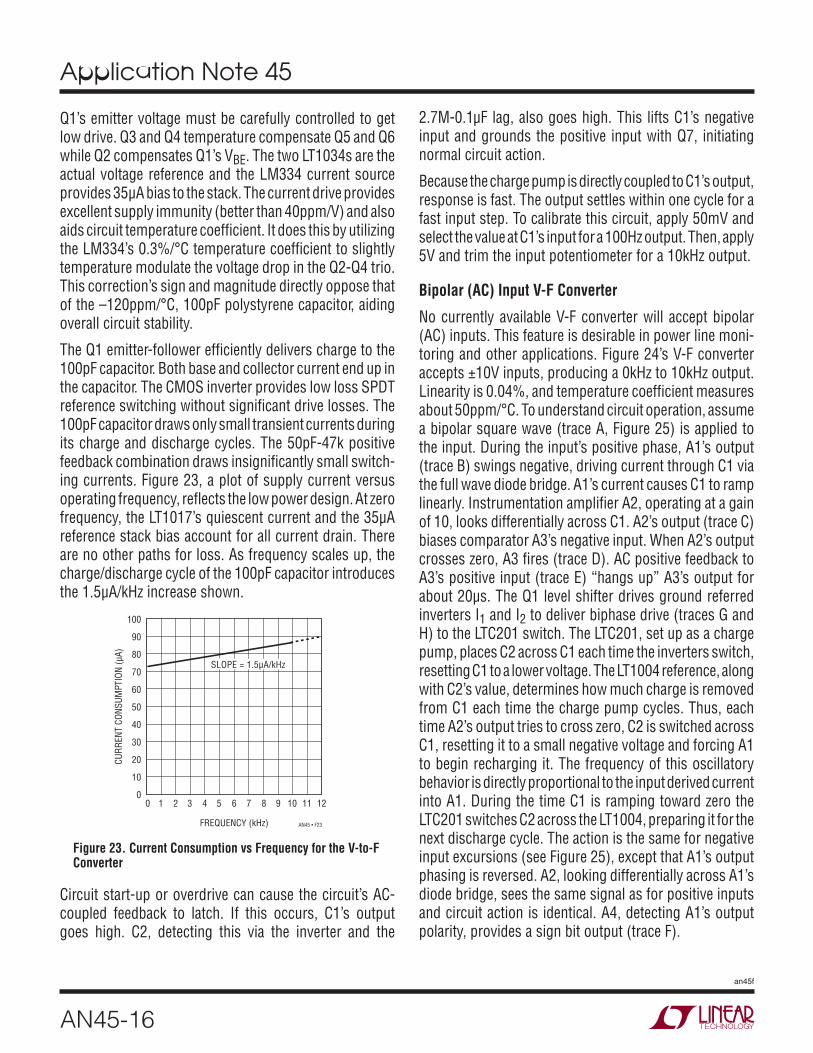
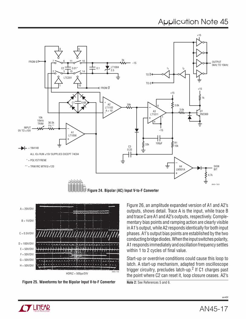
Bipolar (AC) Input V-F Converter
No currently available V-F converter will accept bipolar (AC) inputs. This feature is desirable in power line moni-toring and other applications. Figure 24’s V-F converter accepts ±10V inputs, producing a 0kHz to 10kHz output. Linearity is 0.04%, and temperature coefficient measures about 50ppm/°C. To understand circuit operation, assume a bipolar square wave (trace A, Figure 25) is applied to the input. During the input’s positive phase, A1’s output (trace B) swings negative, driving current through C1 via the full wave diode bridge. A1’s current causes C1 to ramp linearly. Instrumentation amplifier A2, operating at a gain of 10, looks differentially across C1. A2’s output (trace C) biases comparator A3’s negative input. When A2’s output crosses zero, A3 fires (trace D). AC positive feedback to A3’s positive input (trace E) “hangs up” A3’s output for about 20μs. The Q1 level shifter drives ground referred inverters I1 and I2 to deliver biphase drive (traces G and H) to the LTC201 switch. The LTC201, set up as a charge pump, places C2 across C1 each time the inverters switch, resetting C1 to a lower voltage. The LT1004 reference, along with C2’s value, determines how much charge is removed from C1 each time the charge pump cycles. Thus, each time A2’s output tries to cross zero, C2 is switched across C1, resetting it to a small negative voltage and forcing A1 to begin recharging it. The frequency of this oscillatory behavior is directly proportional to the input derived current into A1. During the time C1 is ramping toward zero the LTC201 switches C2 across the LT1004, preparing it for the next discharge cycle. The action is the same for negative input excursions (see Figure 25), except that A1’s output phasing is reversed. A2, looking differentially across A1’s diode bridge, sees the same signal as for positive inputs and circuit action is identical. A4, detecting A1’s output polarity, provides a sign bit output (trace F).
Figure 23. Current Consumption vs Frequency for the V-to-F Converter
FREQUENCY (kHz)
0
CURR
ENT
CONS
UMPT
ION
(μA)
100
90
80
70
60
50
40
30
20
10
0121 2 3 4 5 6 7 8 9 10 11
SLOPE = 1.5μA/kHz
Circuit start-up or overdrive can cause the circuit’s AC-coupled feedback to latch. If this occurs, C1’s output goes high. C2, detecting this via the inverter and the
Application Note 45
AN45-17
an45f
0.68 +
–
36.5k
3
67
8 9
–
+
A4
39k–
A3
33k
3.6k
3.6k
4.7k
C30.33
+
+
–
4
8
Figure 24. Bipolar (AC) Input V-to-F Converter
Figure 25. Waveforms for the Bipolar Input V-to-F Converter
HORIZ = 500μs/DIV
D = 100V/DIV
B = 1V/DIV
C = 0.5V/DIV
E = 50V/DIV
G = 50V/DIV
H = 50V/DIV
Figure 26, an amplitude expanded version of A1 and A2’s outputs, shows detail. Trace A is the input, while trace B and trace C are A1 and A2’s outputs, respectively. Comple-mentary bias points and ramping action are clearly visible in A1’s output, while A2 responds identically for both input phases. A1’s output bias points are established by the two conducting bridge diodes. When the input switches polarity, A1 responds immediately and oscillation frequency settles within 1 to 2 cycles of final value.
Start-up or overdrive conditions could cause this loop to latch. A start-up mechanism, adapted from oscilloscope trigger circuitry, precludes latch-up.2 If C1 charges past the point where C2 can reset it, loop closure ceases. A2’s Note 2: See References 5 and 6.
Application Note 45
AN45-18
an45f
output saturates positive, causing A3 to go negative. A3’s prolonged negative state, detected by the R1-C3 filter, pulls its negative input toward –15V. When A3’s negative input crosses zero, its output changes state and charges R1-C3 positively. A3’s input rises above zero, causing output reversal and free-running oscillation commences. As in normal mode, the 100pF-33k RC aids transitions. A3’s oscillations are transmitted to the LTC201 based charge pump via A1 and the inverters. C2 pumps charge out of C1, driving the voltage across it toward zero. A2 comes out of positive saturation and heads negative, eliminating
positive bias at A3’s input. A3’s free-running oscillation stops, and normal loop action begins.
To calibrate this circuit apply either a –10V or a +10V input and set the 10kΩ trimmer for exactly 10kHz output. The low offsets of A1 and A2 permit operation down to a few hertz with no zero trim required.
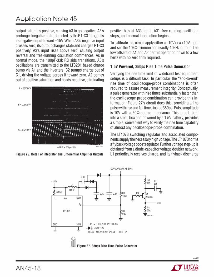
1.5V Powered, 350ps Rise Time Pulse Generator
Verifying the rise time limit of wideband test equipment setups is a difficult task. In particular, the “end-to-end” rise time of oscilloscope-probe combinations is often required to assure measurement integrity. Conceptually, a pulse generator with rise times substantially faster than the oscilloscope-probe combination can provide this in-formation. Figure 27’s circuit does this, providing a 1ns pulse with rise and fall times inside 350ps. Pulse amplitude is 10V with a 50Ω source impedance. This circuit, built into a small box and powered by a 1.5V battery, provides a simple, convenient way to verify the rise time capability of almost any oscilloscope-probe combination.
The LT1073 switching regulator and associated compo-nents supply the necessary high voltage. The LT1073 forms a flyback voltage boost regulator. Further voltage step-up is obtained from a diode-capacitor voltage doubler network. L1 periodically receives charge, and its flyback discharge
HORIZ = 500μs/DIV
A = 50V/DIV
B = 0.5V/DIV
Figure 26. Detail of Integrator and Differential Amplifier Outputs
Figure 27. 350ps Rise Time Pulse Generator
I
GND
150μH
B
L VIN SW1
Ω
L1+1.5V 1M
R110M
+90V AVALANCHE BIAS
R450Ω
C1
OUT
L1
Q1
Application Note 45
AN45-19
an45f
delivers high voltage events to the doubler network. A portion of the doubler network’s DC output is fed back to the LT1073 via the R1, R2 divider, closing a control loop.
The regulator’s 90V output is applied to Q1 via the R3-C1 combination. Q1, a 40V breakdown device, non-destruc-tively avalanches when C1 charges high enough.3 The result is a quickly rising, very fast pulse across R4. C1 discharges, Q1’s collector voltage falls and breakdown ceases. C1 then recharges until breakdown again occurs. This action causes free-running oscillation at about 200kHz. Figure 28 shows the output pulse. A 1GHz sampling oscilloscope (Tektronix 556 with 1S1 sampling plug-in) measures the pulse at 10V high with about a 1ns base. Rise time is 350ps, with fall time also indicating 350ps. The figures may actually be faster, as the 1S1 is specified with a 350ps rise time limit.4
HORIZ = 200ps/DIV
VERT = 2V/DIV
Q1 may require selection to get avalanche behavior. Such behavior, while characteristic of the device specified, is not guaranteed by the manufacturer. A sample of 50 Motorola 2N2369s, spread over a 12 year date code span, yielded 82%. All “good” devices switched in less than 600ps. C1 is selected for a 10V amplitude output. Value spread is typically 2pF to 4pF. Ground plane type construction with high speed layout techniques are essential for good results from this circuit. Current drain from the 1.5V battery ver-sion is about 5mA.
Figure 28. Avalanche Pulse Generator Output Pulse. Waveform Has 350ps Rise and Fall Times. Slightly Under Damped Turn-Off Is Probably Due to Test Fixture Limitations
Note 3: See References 7.Note 4: I’m sorry, but 1GHz is the fastest scope in my house.
L1
INV
OUT TO 1MΩ
1M
INV
CV
V
1N4148
Q1
+
+
+
Figure 29. Alternate 90V DC-DC Converter
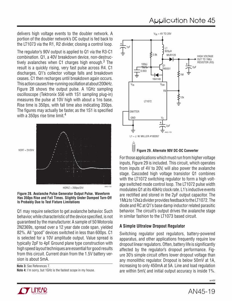
For those applications which must run from higher voltage inputs, Figure 29 is included. This circuit, which operates from inputs of 4V to 20V, will also power the avalanche stage. Cascoded high voltage transistor Q1 combines with the LT1072 switching regulator to form a high volt-age switched mode control loop. The LT1072 pulse width modulates Q1 at its 40kHz clock rate. L1’s inductive events are rectified and stored in the 2μF output capacitor. The 1MΩ to 12kΩ divider provides feedback to the LT1072. The diode and RC at Q1’s base damp inductor related parasitic behavior. The circuit’s output drives the avalanche stage in similar fashion to the LT1073 based circuit.
A Simple Ultralow Dropout Regulator
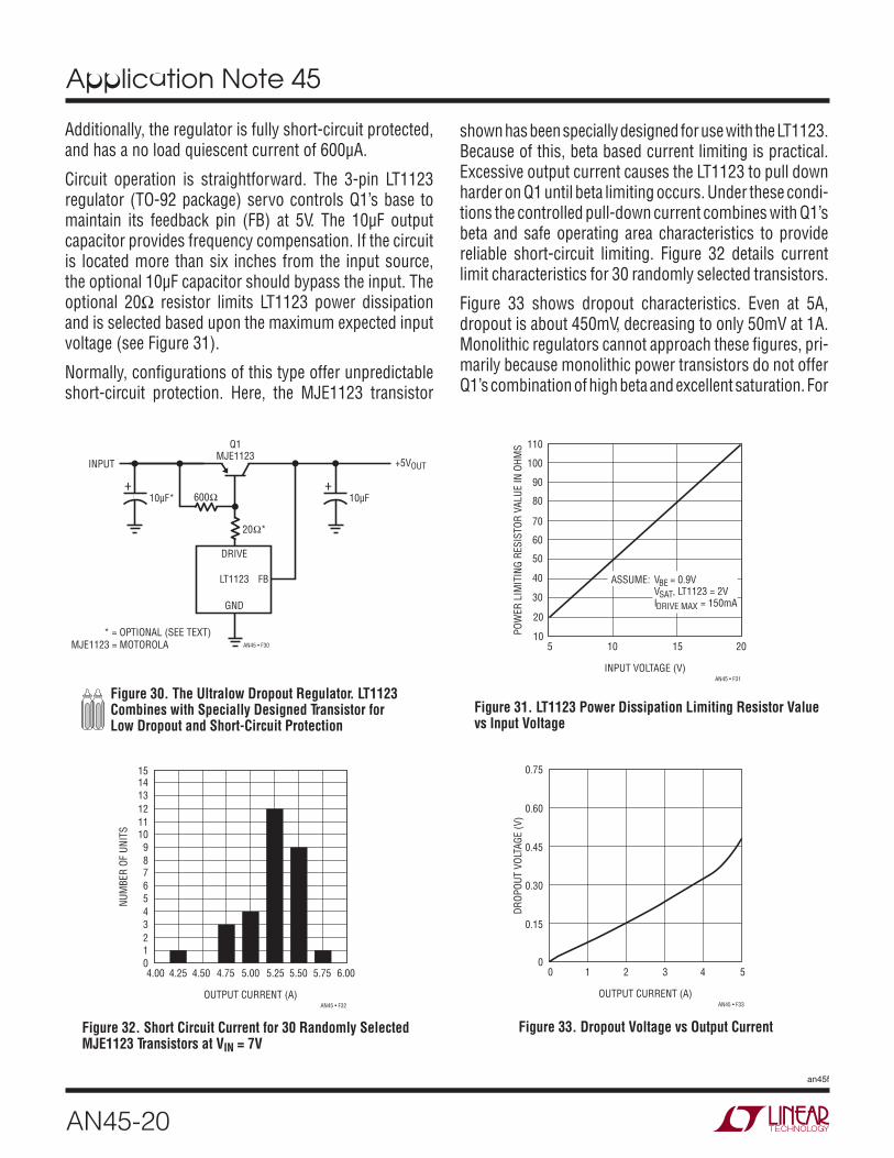
Switching regulator post regulators, battery-powered apparatus, and other applications frequently require low dropout linear regulators. Often, battery life is significantly affected by the regulator’s dropout performance. Fig-ure 30’s simple circuit offers lower dropout voltage than any monolithic regulator. Dropout is below 50mV at 1A, increasing to only 450mA at 5A. Line and load regulation are within 5mV, and initial output accuracy is inside 1%.
Application Note 45
AN45-20
an45f
Additionally, the regulator is fully short-circuit protected, and has a no load quiescent current of 600μA.
Circuit operation is straightforward. The 3-pin LT1123 regulator (TO-92 package) servo controls Q1’s base to maintain its feedback pin (FB) at 5V. The 10μF output capacitor provides frequency compensation. If the circuit is located more than six inches from the input source, the optional 10μF capacitor should bypass the input. The optional 20Ω resistor limits LT1123 power dissipation and is selected based upon the maximum expected input voltage (see Figure 31).
Normally, configurations of this type offer unpredictable short-circuit protection. Here, the MJE1123 transistor
shown has been specially designed for use with the LT1123. Because of this, beta based current limiting is practical. Excessive output current causes the LT1123 to pull down harder on Q1 until beta limiting occurs. Under these condi-tions the controlled pull-down current combines with Q1’s beta and safe operating area characteristics to provide reliable short-circuit limiting. Figure 32 details current limit characteristics for 30 randomly selected transistors.
Figure 33 shows dropout characteristics. Even at 5A, dropout is about 450mV, decreasing to only 50mV at 1A. Monolithic regulators cannot approach these figures, pri-marily because monolithic power transistors do not offer Q1’s combination of high beta and excellent saturation. For
Figure 30. The Ultralow Dropout Regulator. LT1123 Combines with Specially Designed Transistor for Low Dropout and Short-Circuit Protection
Figure 32. Short Circuit Current for 30 Randomly Selected MJE1123 Transistors at VIN = 7V
Figure 31. LT1123 Power Dissipation Limiting Resistor Value vs Input Voltage
Figure 33. Dropout Voltage vs Output Current
OUT+5V
Q1MJE1123
INPUT
10μF* 600Ω
20Ω
DRIVE
LT1123
GND
10μF
FB
* = OPTIONAL (SEE TEXT)MJE1123 = MOTOROLA
*
+ +
INPUT VOLTAGE (V)
5
POW
ER L
IMIT
ING
RESI
STOR
VAL
UE IN
OHM
S
10
20
50
70
90
110
10 15 20
40
60
80
100
BEV = 0.9V
I = 150mA SAT
DRIVE MAX
ASSUME:
OUTPUT CURRENT (A)
4.000
NUM
BER
OF U
NITS
23456
15
4.25 5.00 5.50 5.754.50 4.75 5.25 6.00
1
789
1011121314
OUTPUT CURRENT (A)
00
DROP
OUT
VOLT
AGE
(V)
0.15
0.75
1 2 4 5
0.45
0.60
Application Note 45
AN45-21
an45f
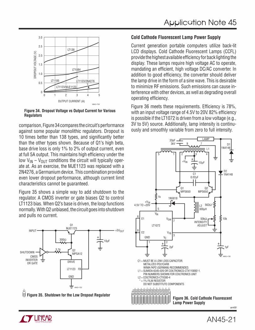
comparison, Figure 34 compares the circuit’s performance against some popular monolithic regulators. Dropout is 10 times better than 138 types, and significantly better than the other types shown. Because of Q1’s high beta, base drive loss is only 1% to 2% of output current, even at full 5A output. This maintains high efficiency under the low VIN – VOUT conditions the circuit will typically oper-ate at. As an exercise, the MJE1123 was replaced with a 2N4276, a Germanium device. This combination provided even lower dropout performance, although current limit characteristics cannot be guaranteed.
Figure 35 shows a simple way to add shutdown to the regulator. A CMOS inverter or gate biases Q2 to control LT1123 bias. When Q2’s base is driven, the loop functions normally. With Q2 unbiased, the circuit goes into shutdown and pulls no current.
OUTPUT CURRENT (A)
0
DROP
OUT
VOLT
AGE
(V)
0.5
3.0
1 2 4 53
1.0
1.5
2.0
LT138
LT1123/MJE1123
LT1123/2N4276LT1185
LT1084
2.5
0
Figure 34. Dropout Voltage vs Output Current for Various Regulators
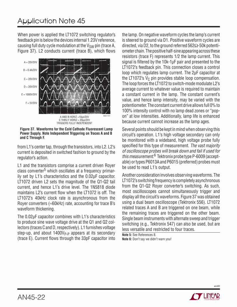
Figure 35. Shutdown for the Low Dropout RegulatorFigure 36. Cold Cathode Fluorescent Lamp Power Supply
Cold Cathode Fluorescent Lamp Power Supply
Current generation portable computers utilize back-lit LCD displays. Cold Cathode Fluorescent Lamps (CCFL) provide the highest available efficiency for back lighting the display. These lamps require high voltage AC to operate, mandating an efficient, high voltage DC/AC converter. In addition to good efficiency, the converter should deliver the lamp drive in the form of a sine wave. This is desirable to minimize RF emissions. Such emissions can cause in-terference with other devices, as well as degrading overall operating efficiency.
Figure 36 meets these requirements. Efficiency is 78%, with an input voltage range of 4.5V to 20V. 82% efficiency is possible if the LT1072 is driven from a low voltage (e.g., 3V to 5V) source. Additionally, lamp intensity is continu-ously and smoothly variable from zero to full intensity.
OUT+5V
Q1MJE1123
300Ω
Q2MPSA12
DRIVE
LT1123
GND
10μF
FB
SHUTDOWN
INPUT
5.1k
CMOSINVERTER
OR GATE
+
D21N4148
Q2MPS650
1N5818
D11N4148
50kΩINTENSITY
ADJUST
562Ω*
10k
1k
LAMP33pF3kV 9 7
43215
Q1MPS650
10μF
C10.02μF
+VIN
+V 4.5V TO +20V
IN
VIN
VSW
VFB
VCGND
E2
E1
LT1072
5
7
3
2μF
1
8
6
2
1μF
L2300μH
L1
C1 = MUST BE A LOW LOSS CAPACITOR. METALIZED POLYCARB WIMA FKP2 (GERMAN) RECOMMENDED.L1 = SUMIDA-6345-020 OR COILTRONICS-CTX110092-1. PIN NUMBERS SHOWN FOR COILTRONICS UNITL2 = COILTRONICS-CTX300-4* = 1% FILM RESISTOR DO NOT SUBSTITUTE COMPONENTS
+
+
+
Application Note 45
AN45-22
an45f
When power is applied the LT1072 switching regulator’s feedback pin is below the devices internal 1.23V reference, causing full duty cycle modulation at the VSW pin (trace A, Figure 37). L2 conducts current (trace B), which flows
A AND B HORIZ =10μs/DIV
F = 5V/DIV
E = 1000V/DIV
D = 20V/DIV
C = 20V/DIV
B = 0.4A/DIV
A = 20V/DIV
C THRU F HORIZ = 20μs/DIVTRIGGERS FULLY INDEPENDENT
Figure 37. Waveforms for the Cold Cathode Fluorescent Lamp Power Supply. Note Independent Triggering on Traces A and B and C Through F.
from L1’s center tap, through the transistors, into L2. L2’s current is deposited in switched fashion to ground by the regulator’s action.
L1 and the transistors comprise a current driven Royer class converter5 which oscillates at a frequency primar-ily set by L1’s characteristics and the 0.02μF capacitor. LT1072 driven L2 sets the magnitude of the Q1-Q2 tail current, and hence L1’s drive level. The 1N5818 diode maintains L2’s current flow when the LT1072 is off. The LT1072’s 40kHz clock rate is asynchronous from the Royer converters (≈60kHz) rate, accounting for trace B’s waveform thickening.
The 0.02μF capacitor combines with L1’s characteristics to produce sine wave voltage drive at the Q1 and Q2 col-lectors (traces C and D, respectively). L1 furnishes voltage step-up, and about 1400VP-P appears at its secondary (trace E). Current flows through the 33pF capacitor into
the lamp. On negative waveform cycles the lamp’s current is steered to ground via D1. Positive waveform cycles are directed, via D2, to the ground referred 562Ω-50k potenti-ometer chain. The positive half-sine appearing across these resistors (trace F) represents 1/2 the lamp current. This signal is filtered by the 10k-1μF pair and presented to the LT1072’s feedback pin. This connection closes a control loop which regulates lamp current. The 2μF capacitor at the LT1072’s VC pin provides stable loop compensation. The loop forces the LT1072 to switch-mode modulate L2’s average current to whatever value is required to maintain a constant current in the lamp. The constant current’s value, and hence lamp intensity, may be varied with the potentiometer. The constant current drive allows full 0% to 100% intensity control with no lamp dead zones or “pop-on” at low intensities. Additionally, lamp life is enhanced because current cannot increase as the lamp ages.
Several points should be kept in mind when observing this circuit’s operation. L1’s high voltage secondary can only be monitored with a wideband, high voltage probe fully specified for this type of measurement. The vast majority of oscilloscope probes will break down and fail if used for this measurement.6 Tektronix probe type P-6009 (accept-able) or types P6013A and P6015 (preferred) probes must be used to read L1’s output.
Another consideration involves observing waveforms. The LT1072’s switching frequency is completely asynchronous from the Q1-Q2 Royer converter’s switching. As such, most oscilloscopes cannot simultaneously trigger and display all the circuit’s waveforms. Figure 37 was obtained using a dual beam oscilloscope (Tektronix 556). LT1072 related traces A and B are triggered on one beam, while the remaining traces are triggered on the other beam. Single beam instruments with alternate sweep and trigger switching (e.g., Tektronix 547) can also be used, but are less versatile and restricted to four traces.Note 5: See References 8.Note 6: Don’t say we didn’t warn you!
Application Note 45
AN45-23
an45f
Information furnished by Linear Technology Corporation is believed to be accurate and reliable. However, no responsibility is assumed for its use. Linear Technology Corporation makes no representa-tion that the interconnection of its circuits as described herein will not infringe on existing patent rights.
References
1. Verster, T.C., “P-N Junction as an Ultralinear Calculable Thermometer,” Electronic Letters, Vol. 4, pg. 175, May, 1968.
2. Verster, T.C., “The Silicon Transistor as a Temperature Sensor,” International Symposium on Temperature, 1971, Washington, D.C.
3. Type 7D13 Plug-In Operating and Service Manual, Tektronix, Inc., 1971.
4. Sheingold, D.H., “Nonlinear Circuits Handbook,” Chapter 3-1, “Basic Considerations,” pgs. 165-166,
Analog Devices, Inc., 1974.
5. Oscilloscope Trigger Circuits, “Automatic Trigger,” pgs. 39-49, Tektronix Concept Series, 1969.
6. Type 547 Oscilloscope Operating and Service Manual, “Automatic Stability Circuit,” pgs. 3-8, Tektronix, Inc., 1964.
7. Type 111 Pretrigger Pulse Generator Operating and Service Manual, Tektronix, Inc., 1960.
8. Bright, Pittman and Royer, “Transistors As On-Off Switches in Saturable Core Circuits,” Electrical Manufacturing, December, 1954.
9. Morrison, John C., MD, Editor. “Antepartal Fetal Surveillance,” Obstetrics and Gynecology Clinics of North America, Volume 17:1, March, 1990, W.B. Saunders Co.
10. Atkinson, P., Woodcock, J.P., “Doppler Ultrasound,” London, Academic Press, 1982.
11. Doppler, J.C., “Uber das farbigte Licht der Dopplersterne und einigr anderer Gestirne des Himmels,” Abhandl d Konigl Bomischen Gesellschaft der Wissenschaften 2:466, 1843.
12. FitzGerald, D.E., Drumm, J.E., “Noninvasive measurement of fetal circulation using ultrasound: A new method,” Br Med J 2:1450, 1977.
13. Hata, T., Aoki, S., Hata, K., et al, “Intracardiac blood flow velocity waveforms in normal fetuses in utero,” Am J Cardiol 58:464, 1987.
14. Pourcelot, L., “Applications clinique de l’examen Doppler transcutane,” In Pourcelot, L. (ed), Velocimetric Ultrasonore Doppler, INSERM 34:213, 1974.
15. Shung, K.K., Sigelman, R.A., Reid, J.M., “Scattering of ultrasound by blood,” IEEE Trans Biomed Eng BME-23:460, 1976.
16. Stuart, B., Drumm, J., FitzGerald, D.E., et al, “Fetal blood velocity waveforms in normal pregnancy,” Br J Obstet Gynaecol 87:780, 1980.
17. Stabile, I., Bilardo, C., Panella, M., et al, “Doppler measurement of uterine blood flow in the firsttrimester of normal and complicated pregnancies,” Trophoblast Res 3:301, 1988.
Application Note 45
AN45-24
an45f
Linear Technology Corporation1630 McCarthy Blvd., Milpitas, CA 95035-7417 (408) 432-1900 ● FAX: (408) 434-0507 ● www.linear.com © LINEAR TECHNOLOGY CORPORATION 1991
BA/GP 0691 10K REV 0 • PRINTED IN USA