AN105 - Current Sense Circuit Collection Making Sense of ... · A N 105 AN105-1 an105fa December...
118
Application Note 105 AN105-1 an105fa December 2005 Current Sense Circuit Collection Making Sense of Current Tim Regan, Jon Munson Greg Zimmer, Michael Stokowski L, LT, LTC, LTM, Linear Technology, the Linear logo, Over-The-Top and TimerBlox are registered trademarks and Hot Swap is a trademark of Linear Technology Corporation. All other trademarks are the property of their respective owners. INTRODUCTION Sensing and/or controlling current flow is a fundamen- tal requirement in many electronics systems, and the techniques to do so are as diverse as the applications themselves. This Application Note compiles solutions to current sensing problems and organizes the solutions by general application type. These circuits have been culled from a variety of Linear Technology documents. Circuits Organized by General Application Each chapter collects together applications that tend to solve a similar general problem, such as high side current sensing, or negative supply sensing. The chapters are titled accordingly. In this way, the reader has access to many possible solutions to a particular problem in one place. It is unlikely that any particular circuit shown will exactly meet the requirements for a specific design, but the sug- gestion of many circuit techniques and devices should prove useful. To avoid duplication, circuits relevant to multiple chapters may appear in one location. CIRCUIT COLLECTION INDEX n Current Sense Basics n High Side n Low Side n Negative Voltage n Unidirectional n Bidirectional n AC n DC n Level Shifting n High Voltage n Low Voltage n High Current (100mA to Amps) n Low Current (Picoamps to Milliamps) n Motors and Inductive Loads n Batteries n High Speed n Fault Sensing n Digitizing n Current Control n Precision n Wide Range
Transcript of AN105 - Current Sense Circuit Collection Making Sense of ... · A N 105 AN105-1 an105fa December...

Application Note 105
AN105-1
an105fa
December 2005
Current Sense Circuit CollectionMaking Sense of Current
Tim Regan, Jon MunsonGreg Zimmer, Michael Stokowski
L, LT, LTC, LTM, Linear Technology, the Linear logo, Over-The-Top and TimerBlox are registered trademarks and Hot Swap is a trademark of Linear Technology Corporation. All other trademarks are the property of their respective owners.
INTRODUCTION
Sensing and/or controlling current flow is a fundamen-tal requirement in many electronics systems, and the techniques to do so are as diverse as the applications themselves. This Application Note compiles solutions to current sensing problems and organizes the solutions by general application type. These circuits have been culled from a variety of Linear Technology documents.
Circuits Organized by General Application
Each chapter collects together applications that tend to solve a similar general problem, such as high side current
sensing, or negative supply sensing. The chapters are titled accordingly. In this way, the reader has access to many possible solutions to a particular problem in one place.
It is unlikely that any particular circuit shown will exactly meet the requirements for a specific design, but the sug-gestion of many circuit techniques and devices should prove useful. To avoid duplication, circuits relevant to multiple chapters may appear in one location.
CIRCUIT COLLECTION INDEX
n Current Sense Basicsn High Siden Low Siden Negative Voltagen Unidirectionaln Bidirectionaln ACn DC
n Level Shiftingn High Voltagen Low Voltagen High Current (100mA to Amps)n Low Current (Picoamps to Milliamps)n Motors and Inductive Loadsn Batteries
n High Speedn Fault Sensingn Digitizingn Current Controln Precisionn Wide Range
Application Note 105
AN105-2
an105fa
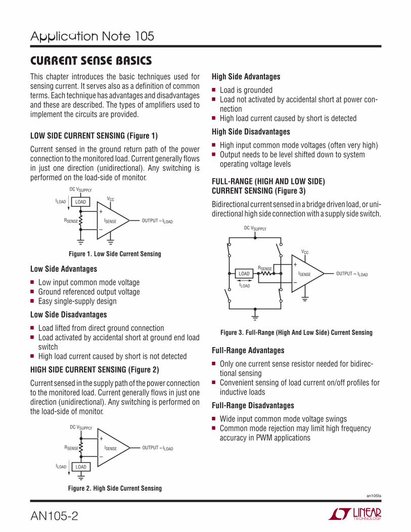
This chapter introduces the basic techniques used for sensing current. It serves also as a definition of common terms. Each technique has advantages and disadvantages and these are described. The types of amplifiers used to implement the circuits are provided.
LOW SIDE CURRENT SENSING (Figure 1)
Current sensed in the ground return path of the power connection to the monitored load. Current generally flows in just one direction (unidirectional). Any switching is performed on the load-side of monitor.
–
+
ILOAD
ISENSE
LOAD
OUTPUT ≈ ILOAD
DC VSUPPLY
VCC
RSENSE
Low Side Advantagesn Low input common mode voltagen Ground referenced output voltagen Easy single-supply design
Low Side Disadvantagesn Load lifted from direct ground connectionn Load activated by accidental short at ground end load
switchn High load current caused by short is not detected
HIGH SIDE CURRENT SENSING (Figure 2)
Current sensed in the supply path of the power connection to the monitored load. Current generally flows in just one direction (unidirectional). Any switching is performed on the load-side of monitor.
–
+
ILOAD
ISENSE
LOAD
OUTPUT ≈ ILOAD
DC VSUPPLY
RSENSE
–
+
ILOAD
ISENSE OUTPUT ∝ ILOAD
DC VSUPPLY
VCC
RSENSELOAD
CURRENT SENSE BASICS
Figure 1. Low Side Current Sensing
Figure 3. Full-Range (High And Low Side) Current Sensing
Figure 2. High Side Current Sensing
High Side Advantagesn Load is groundedn Load not activated by accidental short at power con-
nection n High load current caused by short is detected
High Side Disadvantagesn High input common mode voltages (often very high)n Output needs to be level shifted down to system
operating voltage levels
FULL-RANGE (HIGH AND LOW SIDE) CURRENT SENSING (Figure 3)
Bidirectional current sensed in a bridge driven load, or uni-directional high side connection with a supply side switch.
Full-Range Advantagesn Only one current sense resistor needed for bidirec-
tional sensingn Convenient sensing of load current on/off profiles for
inductive loads
Full-Range Disadvantagesn Wide input common mode voltage swingsn Common mode rejection may limit high frequency
accuracy in PWM applications

Application Note 105
AN105-3
an105fa
HIGH SIDE
Figure 4. LT6100 Load Current Monitor
Figure 5. “Classic” Positive Supply Rail Current Sense
Figure 6. Over-The-Top Current Sense
This chapter discusses solutions for high side current sensing. With these circuits the total current supplied to a load is monitored in the positive power supply line.
LT6100 Load Current Monitor (Figure 4)
This is the basic LT6100 circuit configuration. The internal circuitry, including an output buffer, typically operates from a low voltage supply, such as the 3V shown. The moni-tored supply can range anywhere from VCC + 1.4V up to 48V. The A2 and A4 pins can be strapped various ways to provide a wide range of internally fixed gains. The input leads become very Hi-Z when VCC is powered down, so as not to drain batteries for example. Access to an internal signal node (Pin 3) provides an option to include a filtering function with one added capacitor. Small-signal range is limited by VOL in single-supply operation.
OUTPUTVEEOUT
6100 F04
RSENSE
LT6100
81
VS– VS
+
A42
VCC
A23
4
7
C20.1µF
C10.1µF
3V
6
5
FIL
TO LOAD
+
5V+
– +
–
+LT1637
5V
200Ω
200Ω
0.2Ω
2k
0V TO 4.3V
1637 TA02VOUT = (2Ω)(ILOAD)
Q12N3904
LOAD ILOAD
–
+LT1637
3V TO 44V
3V
R1200Ω
RS0.2Ω
R22k
VOUT(0V TO 2.7V)
Q12N3904
1637 TA06
LOAD
ILOAD
VOUT(RS)(R2/R1)
ILOAD =“Classic” Positive Supply Rail Current Sense (Figure 5)
This circuit uses generic devices to assemble a function similar to an LTC6101. A rail-to-rail input type op amp is required since input voltages are right at the upper rail. The circuit shown here is capable of monitoring up to 44V applications. Besides the complication of extra parts, the VOS performance of op amps at the supply is generally not factory trimmed, thus less accurate than other solutions. The finite current gain of the bipolar transistor is a small source of gain error.
Over-The-Top Current Sense (Figure 6)
This circuit is a variation on the “classic” high side cir-cuit, but takes advantage of Over-the-Top input capability to separately supply the IC from a low voltage rail. This provides a measure of fault protection to downstream circuitry by virtue of the limited output swing set by the low voltage supply. The disadvantage is VOS in the Over-the-Top mode is generally inferior to other modes, thus less accurate. The finite current gain of the bipolar transistor is a source of small gain error.
Self-Powered High Side Current Sense (Figure 7)
This circuit takes advantage of the microampere supply current and rail-to-rail input of the LT1494. The circuit is simple because the supply draw is essentially equal to the load current developed through RA. This supply current is simply passed through RB to form an output voltage that is appropriately amplified.

Application Note 105
AN105-4
an105fa
High Side Current Sense and Fuse Monitor (Figure 8)
The LT6100 can be used as a combination current sen-sor and fuse monitor. This part includes on-chip output buffering and was designed to operate with the low supply voltage (≥2.7V), typical of vehicle data acquisition systems, while the sense inputs monitor signals at the higher bat-tery bus potential. The LT6100 inputs are tolerant of large input differentials, thus allowing the blown-fuse operating condition (this would be detected by an output full-scale indication). The LT6100 can also be powered down while maintaining high impedance sense inputs, drawing less than 1µA max from the battery bus.
HIGH SIDEPrecision High Side Power Supply Current Sense (Figure 9)
This is a low voltage, ultrahigh precision monitor featuring a zero-drift instrumentation amplifier (IA) that provides rail-to-rail inputs and outputs. Voltage gain is set by the feedback resistors. Accuracy of this circuit is set by the quality of resistors selected by the user, small-signal range is limited by VOL in single-supply operation. The voltage rating of this part restricts this solution to applications of <5.5V. This IA is sampled, so the output is discontinuous with input changes, thus only suited to very low frequency measurements.
+
–LT1494
RA1k
RSENSE1Ω
LOAD IL
VS = 2.7V TO 36V
1495 TA09
RB10k
+
_
VO
( )RBRA
VO = IL RS
FOR RA = 1k, RB = 10k, RS = 1Ω
= 10 V/A
OUTPUT OFFSET ≈ IS • RB ≈ 10mVOUTPUT CLIPS AT VS – 2.4V
VOIL
Figure 7. Self-Powered High Side Current Sense
Figure 8. High Side Current Sense and Fuse Monitor
Figure 9. Precision High Side Power Supply Current Sense
OUTPUT2.5V = 25AVEE
OUT
DN374 F02
RSENSE2mΩ FUSE
LT6100
81
VS– VS
+
BATTERYBUS
A4ADC
POWER≥2.7V
2VCC
A23
4
7
C20.1µF
6
5
FIL
TO LOAD
– +
+
–
+LTC6800
45
6
7OUT100mV/AOF LOADCURRENT10k
1.5mΩ
0.1µF
150Ω
6800 TA01
ILOAD
82
VREGULATOR
3
LOAD
Positive Supply Rail Current Sense (Figure 10)
This is a configuration similar to an LT6100 implemented with generic components. A rail-to-rail or Over-the-Top input op amp type is required (for the first section). The first section is a variation on the classic high side where the P-MOSFET provides an accurate output current into R2 (compared to a BJT). The second section is a buffer to allow driving ADC ports, etc., and could be configured with gain if needed. As shown, this circuit can handle up to 36V operation. Small-signal range is limited by VOL in single-supply operation.

Application Note 105
AN105-5
an105fa
CURRENT MONITOR OUTPUT0mA TO 1mA = 0V TO 1V
+
–LT1789
A = 1
BIAS OUTPUTTO APD
VIN10V TO 35V
1N46843.3V
AN92 F02b
1k1%
10M
CURRENT MONITOR OUTPUT0mA TO 1mA = 0V TO 1V
+
–
35V
LT1789
A = 1
BIAS OUTPUTTO APD
VIN10V TO 33V
AN92 F02a
1k1%
Measuring Bias Current Into an Avalanche Photo Diode (APD) Using an Instrumentation Amplifier (Figures 12a and 12b)
The upper circuit (a) uses an instrumentation amplifier (IA) powered by a separate rail (>1V above VIN) to mea-sure across the 1kΩ current shunt. The lower figure (b) is similar but derives its power supply from the APD bias line. The limitation of these circuits is the 35V maximum APD voltage, whereas some APDs may require 90V or more. In the single-supply configuration shown, there is also a dynamic range limitation due to VOL to consider. The advantage of this approach is the high accuracy that is available in an IA.
HIGH SIDE
Figure 10. Positive Supply Rail Current Sense
Figure 11. Precision Current Sensing in Supply Rails
Figure 12b
Figure 12a
–
+1/2 LT1366
R1200Ω
1366 TA01
LOAD
ILOAD
Rs0.2Ω
R220k
Q1TP0610L
VCC
VO = ILOAD • RS
= ILOAD • 20Ω
( )
–
+1/2 LT1366
R2R1
Precision Current Sensing in Supply Rails (Figure 11)
This is the same sampling architecture as used in the front end of the LTC2053 and LTC6800, but sans op amp gain stage. This particular switch can handle up to 18V, so the ultrahigh precision concept can be utilized at higher voltages than the fully integrated ICs mentioned. This circuit simply commutates charge from the flying sense capacitor to the ground-referenced output capacitor so that under DC input conditions the single-ended output voltage is exactly the same as the differential across the sense resistor. A high precision buffer amplifier would typically follow this circuit (such as an LTC2054). The commutation rate is user set by the capacitor connected to Pin 14. For negative supply monitoring, Pin 15 would be tied to the negative rail rather than ground.
6943 • TA01b
0.01µF
9
POSITIVE OR NEGATIVE RAIL
10
11
6
1µF
RSHUNT
I
1/2 LTC6943
12
7
14 15
1µF
E
E ERSHUNT
I =
Figure 12. Measuring Bias Current Into an Avalanche Photo Diode (APD) Using an Instrumentation Amplifier
Application Note 105
AN105-6
an105fa
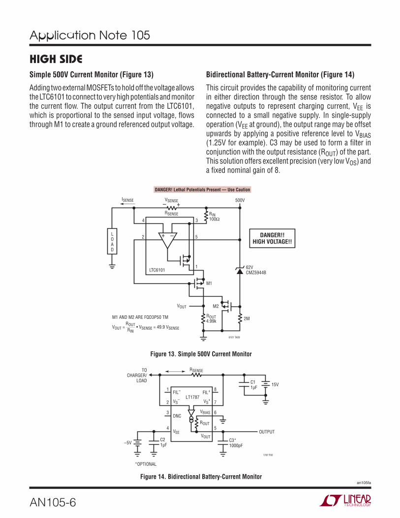
Simple 500V Current Monitor (Figure 13)
Adding two external MOSFETs to hold off the voltage allows the LTC6101 to connect to very high potentials and monitor the current flow. The output current from the LTC6101, which is proportional to the sensed input voltage, flows through M1 to create a ground referenced output voltage.
HIGH SIDE
6101 TA09
LTC6101
RIN100Ω
VOUT
ROUT4.99k
LOAD
–+
VOUT = • VSENSE = 49.9 VSENSEROUTRIN
M1 AND M2 ARE FQD3P50 TM
M1
M2
62VCMZ5944B
500V
2M
VSENSE
RSENSE
ISENSE+–
DANGER! Lethal Potentials Present — Use Caution
DANGER!!HIGH VOLTAGE!!
52
1
34
Bidirectional Battery-Current Monitor (Figure 14)
This circuit provides the capability of monitoring current in either direction through the sense resistor. To allow negative outputs to represent charging current, VEE is connected to a small negative supply. In single-supply operation (VEE at ground), the output range may be offset upwards by applying a positive reference level to VBIAS (1.25V for example). C3 may be used to form a filter in conjunction with the output resistance (ROUT) of the part. This solution offers excellent precision (very low VOS) and a fixed nominal gain of 8.
*OPTIONAL
C21µF–5V
1787 F02
OUTPUT
C3*1000pF
C11µF
RSENSE
15V
TOCHARGER/
LOAD
1
2
3
4
8
7
6
5
LT1787FIL+FIL–
VBIAS
VOUT
VS– VS
+
DNC
VEE
ROUT
Figure 13. Simple 500V Current Monitor
Figure 14. Bidirectional Battery-Current Monitor

Application Note 105
AN105-7
an105fa
HIGH SIDE
Figure 15. LTC6101 Supply Current Included as Load in Measurement
Figure 16. Simple High Side Current Sense Using the LTC6101
Figure 17. High Side Transimpedance Amplifier
LTC6101 Supply Current Included as Load in Measurement (Figure 15)
This is the basic LTC6101 high side sensing supply-monitor configuration, where the supply current drawn by the IC is included in the readout signal. This configuration is use-ful when the IC current may not be negligible in terms of overall current draw, such as in low power battery-powered applications. RSENSE should be selected to limit voltage drop to <500mV for best linearity. If it is desirable not to include the IC current in the readout, as in load monitor-ing, Pin 5 may be connected directly to V+ instead of the load. Gain accuracy of this circuit is limited only by the precision of the resistors selected by the user.
or an H-bridge. The circuit is programmable to produce up to 1mA of full-scale output current into ROUT, yet draws a mere 250µA supply current when the load is off.
LTC6101ROUT
VOUT
6101 F06
3
5
4
2
1
RIN
LOAD
V+
RSENSE
–+
Simple High Side Current Sense Using the LTC6101 (Figure 16)
This is a basic high side current monitor using the LTC6101. The selection of RIN and ROUT establishes the desired gain of this circuit, powered directly from the battery bus. The current output of the LTC6101 allows it to be located re-motely to ROUT. Thus, the amplifier can be placed directly at the shunt, while ROUT is placed near the monitoring electronics without ground drop errors. This circuit has a fast 1µs response time that makes it ideal for providing MOSFET load switch protection. The switch element may be the high side type connected between the sense resistor and the load, a low side type between the load and ground
DN374 F01
LT6101
4
LOAD
BATTERY BUS
RSENSE0.01Ω
RIN100Ω
2
3
5
1 VOUT4.99V = 10A
VOUT = ILOAD(RSENSE • ROUT/RIN)
ROUT4.99k
–+
High Side Transimpedance Amplifier (Figure 17)
Current through a photodiode with a large reverse bias potential is converted to a ground referenced output volt-age directly through an LTC6101. The supply rail can be as high as 70V. Gain of the I to V conversion, the trans- impedance, is set by the selection of resistor RL.
–+
6101 TA04
RL
VO
4.75k4.75k
VS
LASER MONITORPHOTODIODE
CMPZ4697*(10V)
10k
iPD
52
1
34
LTC6101
VO = IPD • RL*VZ SETS PHOTODIODE BIASVZ + 4 ≤ VS ≤ VZ + 60

Application Note 105
AN105-8
an105fa
Intelligent High Side Switch (Figure 18)
The LT1910 is a dedicated high side MOSFET driver with built in protection features. It provides the gate drive for a power switch from standard logic voltage levels. It provides shorted load protection by monitoring the current flow to through the switch. Adding an LTC6101 to the same circuit, sharing the same current sense resistor, provides a linear voltage signal proportional to the load current for additional intelligent control.
48V Supply Current Monitor with Isolated Output and 105V Survivability (Figure 19)
The HV version of the LTC6101 can operate with a total supply voltage of 105V. Current flow in high supply voltage rails can be monitored directly or in an isolated fashion as shown in this circuit. The gain of the circuit and the level of output current from the LTC6101 depends on the particular opto-isolator used.
HIGH SIDE
6101 TA07
LOAD
FAULT
OFF ON
1 54.99k
VORS
3
4
47k
2
8
6
100Ω
100Ω1%
10µF63V
1µF
14VVLOGIC
SUB85N06-5
VO = 49.9 • RS • IL
FOR RS = 5mΩ,VO = 2.5V AT IL = 10A (FULL-SCALE)
LT1910 LTC6101
IL
5
2
1
3
4
6101 TA08
LTC6101HV
RIN
V–
V–
25
43
VSENSE
RSENSE
ISENSE
LOAD
+–
–+
VOUT = VLOGIC – ISENSE • • N • ROUTRSENSE
RIN
N = OPTO-ISOLATOR CURRENT GAIN
VS
ANY OPTO-ISOLATOR
ROUT
VOUT
VLOGIC
Figure 18. Intelligent High Side Switch
Figure 19. 48V Supply Current Monitor with Isolated Output and 105V Survivability

Application Note 105
AN105-9
an105fa
HIGH SIDE
Figure 20. Precision, Wide Dynamic Range High Side Current Sensing
Figure 21. Sensed Current Includes Monitor Circuit Supply Current
Precision, Wide Dynamic Range High Side Current Sensing (Figure 20)
The LTC6102 offers exceptionally high precision (VOS < 10µV) so that a low value sense resistor may be used. This reduces dissipation in the circuit and allows wider variations in current to be accurately measured. In this circuit, the components are scaled for a 10A measuring range, with the offset error corresponding to less than 10mA. This is effectively better than 10-bit dynamic range with dissipation under 100mW.
TO µP
6102 TA01
LTC2433-1ROUT4.99k
VOUT
1µF5V
LOAD
VOUT = • VSENSE = 249.5VSENSEROUTRIN
*PROPER SHUNT SELECTION COULD ALLOWMONITORING OF CURRENTS IN EXCESS OF 1000A
LTC6102
RIN20Ω
VSENSE1mΩ
5V TO105V
V+V–
OUT
+IN
+
–
–INF
–INS
VREG0.1µF
–+
+
Sensed Current Includes Monitor Circuit Supply Current (Figure 21)
To sense all current drawn from a battery power source which is also powering the sensing circuitry requires the proper connection of the supply pin. Connecting the supply pin to the load side of the sense resistor adds the supply current to the load current. The sense amplifier operates properly with the inputs equal to the device V+ supply.
LOAD
–+
6102 TA03
R24.99k
VOUT
R1100
VBATT
RSENSE
LTC6102 +
–VOUT = 49.9 • RSENSE (ILOAD + ISUPPLY)
ILOAD
ISUPPLY
V+V–
OUT
–INS+IN
–INF
VREG0.1µF

Application Note 105
AN105-10
an105fa
HIGH SIDEWide Voltage Range Current Sensing (Figure 22)
The LT6105 has a supply voltage that is independent from the potential at the current sense inputs. The input voltage can extend below ground or exceed the sense amplifier supply voltage. While the sensed current must flow in just one direction, it can be sensed above the load, high side, or below the load, low side. Gain is programmed through resistor scaling and is set to 50 in the circuit shown.
–
+0.02Ω
RIN2100Ω
RIN1100Ω
ROUT4.99k
LT6105
2.85V TO 36VTO LOAD
SOURCE–0.3V TO 44V
VOUT = 1V/AVOUT
V+ V–
VS+
VS–
–IN
+IN
6105 TA01
VOUT = VS
+ − VS–( ) •
ROUT
RIN; A V = ROUT
RIN; RIN1 = RIN2 = RIN
Smooth Current Monitor Output Signal by Simple Filtering (Figure 23)
The output impedance of the LT6105 amplifier is defined by the value of the gain setting output resistor. Bypassing this resistor with a single capacitor provides first order filtering to smooth noisy current signals and spikes.
–
+0.039Ω
249Ω
249Ω 4.99k
LT6105
TO LOAD
SOURCE0V TO 44V
VOUT = 780mV/AVOUT
0.22µF
6105 TA02
2.85V TO 36V
VS+
VS– –IN
+IN
V –
V +
Figure 22. Wide Voltage Range Current Sensing
Figure 23. Smooth Current Monitor Output Signal by Simple Filtering
Application Note 105
AN105-11
an105fa
HIGH SIDE
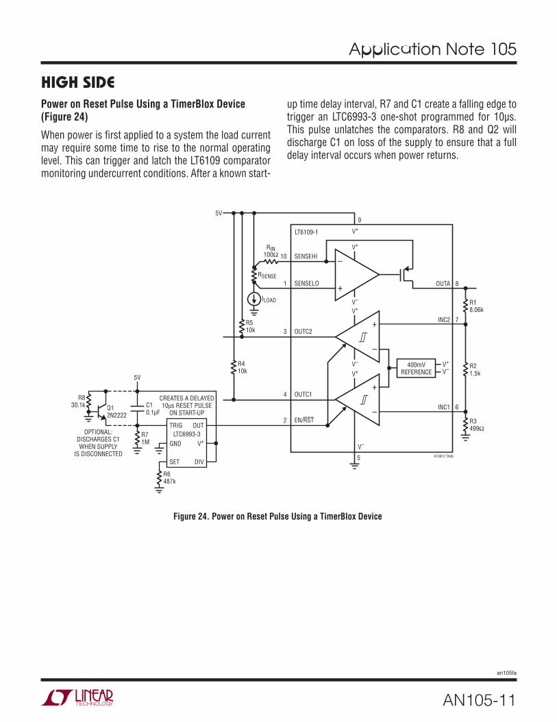
Figure 24. Power on Reset Pulse Using a TimerBlox Device
Power on Reset Pulse Using a TimerBlox Device (Figure 24)
When power is first applied to a system the load current may require some time to rise to the normal operating level. This can trigger and latch the LT6109 comparator monitoring undercurrent conditions. After a known start-
–
+
–
+
V–
V+
V+
V–
–
+
V–
5
INC1
610912 TA06
V+
V–V+
400mVREFERENCE
V+
RIN100Ω
RSENSE
ILOAD
R510k
INC2
OUTA
6
7
8
9
SENSEHI
LT6109-1
5V
SENSELO
OUTC2
OUTC1
EN/RST
10
1
3
4
2
R18.06k
R21.5k
R3499Ω
R410k
R71M
R6487k
R830.1k
TRIG
C10.1µF
Q12N2222
OUT
GND V+
SET DIV
LTC6993-3
5V
CREATES A DELAYED10µs RESET PULSE
ON START-UP
OPTIONAL:DISCHARGES C1WHEN SUPPLY
IS DISCONNECTED
up time delay interval, R7 and C1 create a falling edge to trigger an LTC6993-3 one-shot programmed for 10µs. This pulse unlatches the comparators. R8 and Q2 will discharge C1 on loss of the supply to ensure that a full delay interval occurs when power returns.
Application Note 105
AN105-12
an105fa
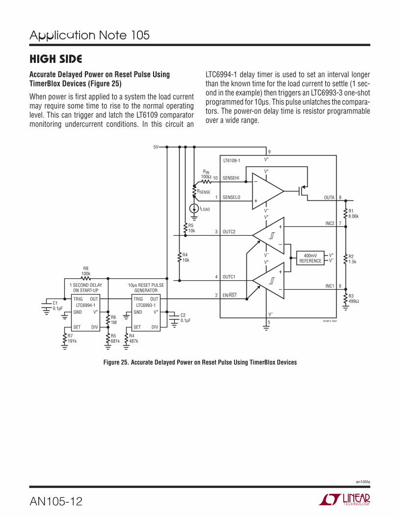
HIGH SIDEAccurate Delayed Power on Reset Pulse Using TimerBlox Devices (Figure 25)
When power is first applied to a system the load current may require some time to rise to the normal operating level. This can trigger and latch the LT6109 comparator monitoring undercurrent conditions. In this circuit an
LTC6994-1 delay timer is used to set an interval longer than the known time for the load current to settle (1 sec-ond in the example) then triggers an LTC6993-3 one-shot programmed for 10µs. This pulse unlatches the compara-tors. The power-on delay time is resistor programmable over a wide range.
–
+
–
+
V–
V+
V+
V–
–
+
V–
5
INC1
610912 TA07
V+
V–V+
400mVREFERENCE
V+
RIN100Ω
RSENSE
ILOAD
R510k
INC2
OUTA
6
7
8
SENSEHI
LT6109-1
95V
SENSELO
OUTC2
OUTC1
EN/RST
10
1
3
4
2
R8100k
R18.06k
R21.5k
R3499Ω
R410k
R4487k
C20.1µF
R5681k
R61M
10µs RESET PULSEGENERATOR
C10.1µF
R7191k
1 SECOND DELAYON START-UP
TRIG OUT
GND V+
SET DIV
LTC6993-1TRIG
GND
SET
LTC6994-1OUT
V+
DIV
Figure 25. Accurate Delayed Power on Reset Pulse Using TimerBlox Devices

Application Note 105
AN105-13
an105fa
HIGH SIDE
FIGURE TITLE40 Monitor Current in Positive or Negative Supply Lines58 Bidirectional Precision Current Sensing59 Differential Output Bidirectional 10A Current Sense60 Absolute Value Output Bidirectional Current Sensing93 High Voltage Current and Temperature Monitoring104 Using Printed Circuit Sense Resistance105 High Voltage, 5A High Side Current Sensing in Small Package120 Bidirectional Current Sensing in H-Bridge Drivers121 Single Output Provides 10A H-Bridge Current and Direction123 Monitor Solenoid Current on the High Side125 Large Input Voltage Range for Fused Solenoid Current Monitoring126 Monitor both the ON Current and the Freewheeling Current Through a High Side Driven Solenoid129 Simple DC Motor Torque Control130 Small Motor Protection and Control131 Large Motor Protection and Control136 Coulomb Counting Battery Gas Gauge142 Monitor Charge and Discharge Currents at One Output143 Battery Stack Monitoring145 High Voltage Battery Coulomb Counting146 Low Voltage Battery Coulomb Counting147 Single Cell Lithium-Ion Battery Coulomb Counter148 Complete Single Cell Battery Protection167 Monitor Current in an Isolated Supply Line168 Monitoring a Fuse Protected Circuit169 Circuit Fault Protection with Early Warning and Latching Load Disconnect170 Use Comparator Output to Initialize Interrupt Routines171 Current Sense with Over-current Latch and Power-On Reset with Loss of Supply176 Directly Digitize Current with 16-Bit Resolution177 Directly Digitizing Two Independent Currents178 Digitize a Bidirectional Current Using a Single Sense Amplifier and ADC179 Digitizing Charging and Loading Current in a Battery Monitor180 Complete Digital Current Monitoring181 Ampere-Hour Gauge182 Power Sensing with Built In A-to-D Converter183 Isolated Power Measurement184 Fast Data Rate Isolated Power Measurement185 Adding Temperature Measurement to Supply Power Measurement186 Current, Voltage and Fuse Monitoring187 Automotive Socket Power Monitoring
More High Side Circuits Are Shown in Other Chapters:

Application Note 105
AN105-14
an105fa
FIGURE TITLE188 Power over Ethernet, PoE, Monitoring189 Monitor Current, Voltage and Temperature208 Remote Current Sensing with Minimal Wiring209 Use Kelvin Connections to Maintain High Current Accuracy210 Crystal/Reference Oven Controller211 Power Intensive Circuit Board Monitoring212 Crystal/Reference Oven Controller215 0 to 10A Sensing Over Two Ranges216 Dual Sense Amplifier Can Have Different Sense Resistors and Gain
HIGH SIDEMore High Side Circuits Are Shown in Other Chapters:
Application Note 105
AN105-15
an105fa
This chapter discusses solutions for low side current sensing. With these circuits the current flowing in the ground return or negative power supply line is monitored.
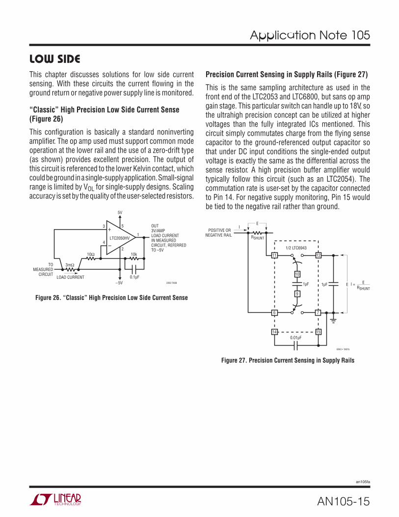
“Classic” High Precision Low Side Current Sense (Figure 26)
This configuration is basically a standard noninverting amplifier. The op amp used must support common mode operation at the lower rail and the use of a zero-drift type (as shown) provides excellent precision. The output of this circuit is referenced to the lower Kelvin contact, which could be ground in a single-supply application. Small-signal range is limited by VOL for single-supply designs. Scaling accuracy is set by the quality of the user-selected resistors.
Precision Current Sensing in Supply Rails (Figure 27)
This is the same sampling architecture as used in the front end of the LTC2053 and LTC6800, but sans op amp gain stage. This particular switch can handle up to 18V, so the ultrahigh precision concept can be utilized at higher voltages than the fully integrated ICs mentioned. This circuit simply commutates charge from the flying sense capacitor to the ground-referenced output capacitor so that under DC input conditions the single-ended output voltage is exactly the same as the differential across the sense resistor. A high precision buffer amplifier would typically follow this circuit (such as an LTC2054). The commutation rate is user-set by the capacitor connected to Pin 14. For negative supply monitoring, Pin 15 would be tied to the negative rail rather than ground.
LOW SIDE
Figure 26. “Classic” High Precision Low Side Current Sense
Figure 27. Precision Current Sensing in Supply Rails
–
+LTC2050HV
1
4
3
2050 TA08
5
2
5V
–5V
TOMEASURED
CIRCUIT
OUT 3V/AMPLOAD CURRENTIN MEASUREDCIRCUIT, REFERRED TO –5V
10Ω 10k
3mΩ
0.1µFLOAD CURRENT
6943 • TA01b
0.01µF
9
POSITIVE OR NEGATIVE RAIL
10
11
6
1µF
RSHUNT
I
1/2 LTC6943
12
7
14 15
1µF
E
E ERSHUNT
I =
Application Note 105
AN105-16
an105fa
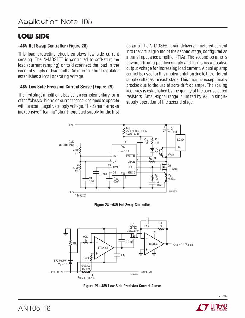
–48V Hot Swap Controller (Figure 28)
This load protecting circuit employs low side current sensing. The N-MOSFET is controlled to soft-start the load (current ramping) or to disconnect the load in the event of supply or load faults. An internal shunt regulator establishes a local operating voltage.
–48V Low Side Precision Current Sense (Figure 29)
The first stage amplifier is basically a complementary form of the “classic” high side current sense, designed to operate with telecom negative supply voltage. The Zener forms an inexpensive “floating” shunt-regulated supply for the first
LOW SIDEop amp. The N-MOSFET drain delivers a metered current into the virtual ground of the second stage, configured as a transimpedance amplifier (TIA). The second op amp is powered from a positive supply and furnishes a positive output voltage for increasing load current. A dual op amp cannot be used for this implementation due to the different supply voltages for each stage. This circuit is exceptionally precise due to the use of zero-drift op amps. The scaling accuracy is established by the quality of the user-selected resistors. Small-signal range is limited by VOL in single-supply operation of the second stage.
425212 TA01
GND
OV
UV
VEE
VIN
1
2
7
6
8
9
10
3 4
5
SENSESS
TIMER GATE
PWRGD
DRAIN
LTC4252-1R1
402k1%
R232.4k
1% CT0.33µF
CSS68nF CC
18nF
–48V
RS0.02Ω
Q1IRF530S
VOUT
RC10Ω
R35.1k
RIN3× 1.8k IN SERIES1/4W EACH
C110nF
CIN1µF
CL100µF
GND(SHORT PIN)
+
RD 1M
LOAD
EN
*
* M0C207
–
+
0.01µF
0.1µF
0.1µF
0.003Ω1% 3W
39k
BZX84C5V1VZ = 5.1
–48V SUPPLY
ISENSE, VSENSE– +
100Ω1%
LTC2054
20545 TA01
–
+
10k1%
5V
VOUT = 100VSENSELTC2054
–48V LOAD
Q1ZETEX
ZVN3320F
100Ω
Figure 28.–48V Hot Swap Controller
Figure 29.–48V Low Side Precision Current Sense
Application Note 105
AN105-17
an105fa
LOW SIDE
Figure 30. Fast Compact –48V Current Sense
Figure 31b
Figure 31a
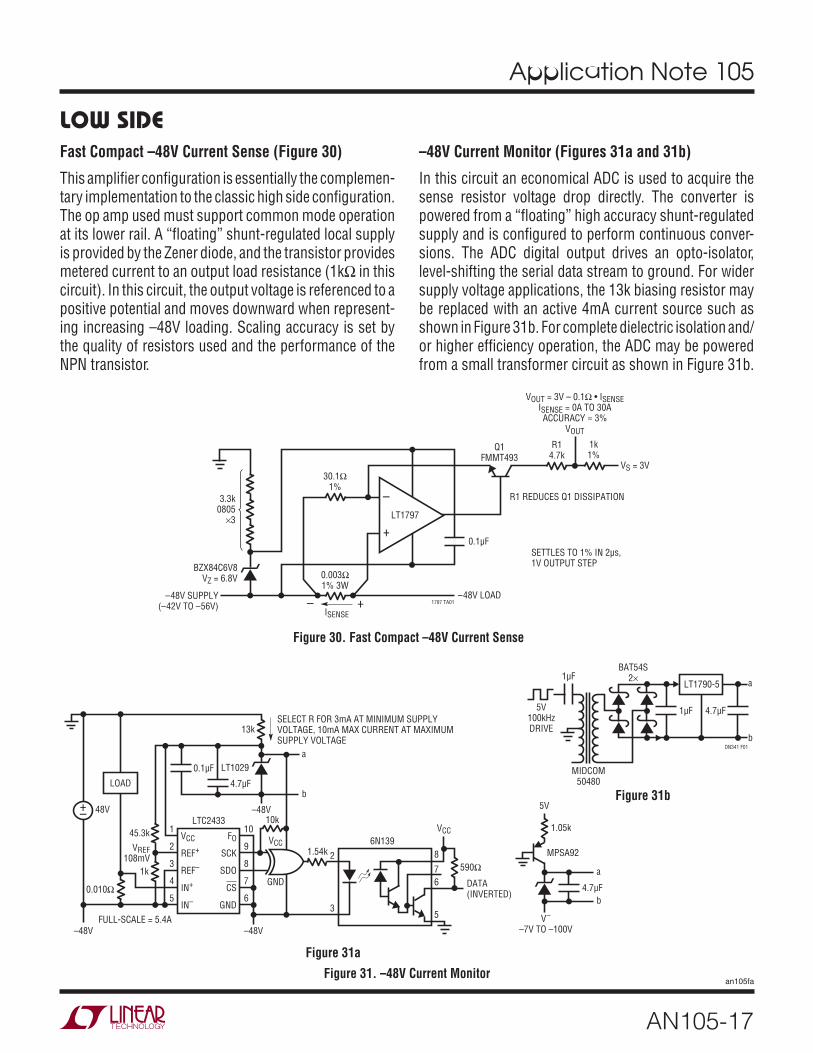
Fast Compact –48V Current Sense (Figure 30)
This amplifier configuration is essentially the complemen-tary implementation to the classic high side configuration. The op amp used must support common mode operation at its lower rail. A “floating” shunt-regulated local supply is provided by the Zener diode, and the transistor provides metered current to an output load resistance (1kΩ in this circuit). In this circuit, the output voltage is referenced to a positive potential and moves downward when represent-ing increasing –48V loading. Scaling accuracy is set by the quality of resistors used and the performance of the NPN transistor.
–48V Current Monitor (Figures 31a and 31b)
In this circuit an economical ADC is used to acquire the sense resistor voltage drop directly. The converter is powered from a “floating” high accuracy shunt-regulated supply and is configured to perform continuous conver-sions. The ADC digital output drives an opto-isolator, level-shifting the serial data stream to ground. For wider supply voltage applications, the 13k biasing resistor may be replaced with an active 4mA current source such as shown in Figure 31b. For complete dielectric isolation and/or higher efficiency operation, the ADC may be powered from a small transformer circuit as shown in Figure 31b.
–
+LT1797
0.1µF
R1 REDUCES Q1 DISSIPATION
Q1FMMT493
0.003Ω1% 3W
BZX84C6V8VZ = 6.8V
–48V SUPPLY(–42V TO –56V)
3.3k0805
×3
30.1Ω1%
ISENSE+–
R14.7k
VS = 3V
1k1%
VOUT = 3V – 0.1Ω • ISENSEISENSE = 0A TO 30AACCURACY ≈ 3%
–48V LOAD1797 TA01
SETTLES TO 1% IN 2µs,1V OUTPUT STEP
VOUT
VCC
REF+
REF–
IN+
IN–
FO
SCK
SDO
CS
GND
1
2
3
4
5
10
9
8
7
6
LTC2433
VREF108mV
–48V–48V
–48V
1k
FULL-SCALE = 5.4A
0.010Ω
45.3k
48V
13k
VCC
GND
1.54k
10k
2
3
8
76
5
4.7µFb
aLT1029
SELECT R FOR 3mA AT MINIMUM SUPPLY VOLTAGE, 10mA MAX CURRENT AT MAXIMUM SUPPLY VOLTAGE
0.1µF
590Ω
DATA(INVERTED)
VCC6N139
LOAD
+–5V
MPSA92
1.05k
V–
–7V TO –100V
4.7µF
a
b
DN341 F01
1µF
5V100kHzDRIVE
MIDCOM50480
BAT54S2×
LT1790-5
4.7µF1µF
a
b
Figure 31. –48V Current Monitor

Application Note 105
AN105-18
an105fa
–48V Hot Swap Controller (Figure 32)
This load protecting circuit employs low side current sensing. The N-MOSFET is controlled to soft-start the load (current ramping) or to disconnect the load in the event of supply or load faults. An internal shunt regulator establishes a local operating voltage.
Simple Telecom Power Supply Fuse Monitor (Figure 33)
The LTC1921 provides an all-in-one telecom fuse and supply voltage monitoring function. Three opto-isolated status flags are generated that indicate the condition of the supplies and the fuses.
LOW SIDE
425212 TA01
GND
OV
UV
VEE
VIN
1
2
7
6
8
9
10
3 4
5
SENSESS
TIMER GATE
PWRGD
DRAIN
LTC4252-1R1
402k1%
R232.4k
1% CT0.33µF
CSS68nF CC
18nF
–48V
RS0.02Ω
Q1IRF530S
VOUT
RC10Ω
R35.1k
RIN3× 1.8k IN SERIES1/4W EACH
C110nF
CIN1µF
CL100µF
GND(SHORT PIN)
+
RD 1M
LOAD
EN
*
* M0C207
Figure 32.–48V Hot Swap Controller
Figure 33. Simple Telecom Power Supply Fuse Monitor
MOC207
MOC207
MOC207
FUSESTATUS
SUPPLY ASTATUS
5V47k
5V47k
5V47k
R347k1/4W
SUPPLY BSTATUS
OK: WITHIN SPECIFICATIONOV: OVERVOLTAGEUV: UNDERVOLTAGE
–48V OUT
= LOGIC COMMON
0: LED/PHOTODIODE ON1: LED/PHOTODIODE OFF*IF BOTH FUSES (F1 AND F2) ARE OPEN, ALL STATUS OUTPUTS WILL BE HIGH SINCE R3 WILL NOT BE POWERED
OUT F
–48VRETURN
VA
3
4
57
2
8
1
6
VB
FUSE A
F1 D1
D2F2
RTN
LTC1921
FUSE B OUT A
OUT B
SUPPLY A–48V
SUPPLY B–48V
R1100k
R2100k
SUPPLY ASTATUS
0011
VBOK
UV OR OVOK
UV OR OV
VAOKOK
UV OR OVUV OR OV
SUPPLY BSTATUS
0101
FUSE STATUS011
1*
VFUSE B= VB≠ VB= VB≠ VB
VFUSE A= VA= VA≠ VA≠ VA

Application Note 105
AN105-19
an105fa
LOW SIDEMore Low Side Circuits Are Shown in Other Chapters:
FIGURE TITLE22 Wide Voltage Range Current Sensing23 Smooth Current Monitor Output Signal by Simple Filtering40 Monitor Current in Positive or Negative Supply Lines122 Monitor Solenoid Current on the Low Side127 Monitor both the ON Current and the Freewheeling Current In a Low Side Driven Solenoid168 Monitoring a Fuse Protected Circuit

Application Note 105
AN105-20
an105fa
NEGATIVE VOLTAGE
Figure 34. Telecom Supply Current Monitor
Figure 35.–48V Hot Swap Controller
This chapter discusses solutions for negative voltage current sensing.
Telecom Supply Current Monitor (Figure 34)
The LT1990 is a wide common mode range difference amplifier used here to amplify the sense resistor drop by ten. To provide the desired input range when using a single 5V supply, the reference potential is set to approximately 4V by the LT6650. The output signal moves downward from the reference potential in this connection so that a large output swing can be accommodated.
–48V Hot Swap Controller (Figure 35)
This load protecting circuit employs low side current sensing. The N-MOSFET is controlled to soft-start the load (current ramping) or to disconnect the load in the event of supply or load faults. An internal shunt regulator establishes a local operating voltage.
–
+
LT6650 GND
IN OUT
FB
174k
20k
1nF
1µF
VREF = 4V
1
2
3
2
65
7
41
8
4 5
LOAD
RS
48VIL
+
–
5V
VOUT
1990 AI01
–77V ≤ VCM ≤ 8VVOUT = VREF – (10 • IL • RS)
LT1990
REF
G1
G2
425212 TA01
GND
OV
UV
VEE
VIN
1
2
7
6
8
9
10
3 4
5
SENSESS
TIMER GATE
PWRGD
DRAIN
LTC4252-1R1
402k1%
R232.4k
1% CT0.33µF
CSS68nF CC
18nF
–48V
RS0.02Ω
Q1IRF530S
VOUT
RC10Ω
R35.1k
RIN3× 1.8k IN SERIES1/4W EACH
C110nF
CIN1µF
CL100µF
GND(SHORT PIN)
+
RD 1M
LOAD
EN
*
* M0C207

Application Note 105
AN105-21
an105fa
NEGATIVE VOLTAGE–48V Low Side Precision Current Sense (Figure 36)
The first stage amplifier is basically a complementary form of the “classic” high side current sense, designed to operate with telecom negative supply voltage. The Zener forms an inexpensive “floating” shunt-regulated supply for the first op amp. The N-MOSFET drain delivers a metered current into the virtual ground of the second stage, configured as a transimpedance amplifier (TIA). The second op amp is powered from a positive supply and furnishes a positive output voltage for increasing load current. A dual op amp cannot be used for this implementation due to the different supply voltages for each stage. This circuit is exceptionally precise due to the use of zero-drift op amps. The scaling accuracy is established by the quality of the user-selected resistors. Small-signal range is limited by VOL in single-supply operation of the second stage.
Fast Compact –48V Current Sense (Figure 37)
This amplifier configuration is essentially the complemen-tary implementation to the classic high side configuration. The op amp used must support common mode operation at its lower rail. A “floating” shunt-regulated local supply is provided by the Zener diode, and the transistor provides metered current to an output load resistance (1kΩ in this circuit). In this circuit, the output voltage is referenced to a positive potential and moves downward when represent-ing increasing –48V loading. Scaling accuracy is set by the quality of resistors used and the performance of the NPN transistor.
–
+
0.01µF
0.1µF
0.1µF
0.003Ω1% 3W
39k
BZX84C5V1VZ = 5.1
–48V SUPPLY
ISENSE, VSENSE– +
100Ω1%
LTC2054
20545 TA01
–
+
10k1%
5V
VOUT = 100VSENSELTC2054
–48V LOAD
Q1ZETEX
ZVN3320F
100Ω
–
+LT1797
0.1µF
R1 REDUCES Q1 DISSIPATION
Q1FMMT493
0.003Ω1% 3W
BZX84C6V8VZ = 6.8V
–48V SUPPLY(–42V TO –56V)
3.3k0805
×3
30.1Ω1%
ISENSE+–
R14.7k
VS = 3V
1k1%
VOUT = 3V – 0.1Ω • ISENSEISENSE = 0A TO 30AACCURACY ≈ 3%
–48V LOAD1797 TA01
SETTLES TO 1% IN 2µs,1V OUTPUT STEP
VOUT
Figure 36.–48V Low Side Precision Current Sense
Figure 37. Fast Compact –48V Current Sense
Application Note 105
AN105-22
an105fa
NEGATIVE VOLTAGE
Figure 39. Simple Telecom Power Supply Fuse Monitor
Figure 38a
Figure 38b
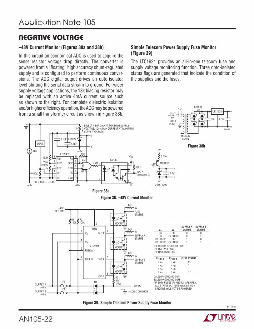
–48V Current Monitor (Figures 38a and 38b)
In this circuit an economical ADC is used to acquire the sense resistor voltage drop directly. The converter is powered from a “floating” high accuracy shunt-regulated supply and is configured to perform continuous conver-sions. The ADC digital output drives an opto-isolator, level-shifting the serial data stream to ground. For wider supply voltage applications, the 13k biasing resistor may be replaced with an active 4mA current source such as shown to the right. For complete dielectric isolation and/or higher efficiency operation, the ADC may be powered from a small transformer circuit as shown in Figure 38b.
Simple Telecom Power Supply Fuse Monitor (Figure 39)
The LTC1921 provides an all-in-one telecom fuse and supply voltage monitoring function. Three opto-isolated status flags are generated that indicate the condition of the supplies and the fuses.
VCC
REF+
REF–
IN+
IN–
FO
SCK
SDO
CS
GND
1
2
3
4
5
10
9
8
7
6
LTC2433
VREF108mV
–48V–48V
–48V
1k
FULL-SCALE = 5.4A
0.010Ω
45.3k
48V
13k
VCC
GND
1.54k
10k
2
3
8
76
5
4.7µFb
aLT1029
SELECT R FOR 3mA AT MINIMUM SUPPLY VOLTAGE, 10mA MAX CURRENT AT MAXIMUM SUPPLY VOLTAGE
0.1µF
590Ω
DATA(INVERTED)
VCC6N139
LOAD
+–5V
MPSA92
1.05k
V–
–7V TO –100V
4.7µF
a
b
DN341 F01
1µF
5V100kHzDRIVE
MIDCOM50480
BAT54S2×
LT1790-5
4.7µF1µF
a
b
MOC207
MOC207
MOC207
FUSESTATUS
SUPPLY ASTATUS
5V47k
5V47k
5V47k
R347k1/4W
SUPPLY BSTATUS
OK: WITHIN SPECIFICATIONOV: OVERVOLTAGEUV: UNDERVOLTAGE
–48V OUT
= LOGIC COMMON
0: LED/PHOTODIODE ON1: LED/PHOTODIODE OFF*IF BOTH FUSES (F1 AND F2) ARE OPEN, ALL STATUS OUTPUTS WILL BE HIGH SINCE R3 WILL NOT BE POWERED
OUT F
–48VRETURN
VA
3
4
57
2
8
1
6
VB
FUSE A
F1 D1
D2F2
RTN
LTC1921
FUSE B OUT A
OUT B
SUPPLY A–48V
SUPPLY B–48V
R1100k
R2100k
SUPPLY ASTATUS
0011
VBOK
UV OR OVOK
UV OR OV
VAOKOK
UV OR OVUV OR OV
SUPPLY BSTATUS
0101
FUSE STATUS011
1*
VFUSE B= VB≠ VB= VB≠ VB
VFUSE A= VA= VA≠ VA≠ VA
Figure 38. –48V Current Monitor
Application Note 105
AN105-23
an105fa
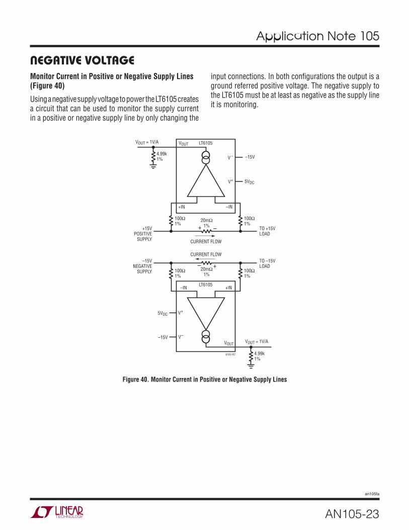
Monitor Current in Positive or Negative Supply Lines (Figure 40)
Using a negative supply voltage to power the LT6105 creates a circuit that can be used to monitor the supply current in a positive or negative supply line by only changing the
NEGATIVE VOLTAGEinput connections. In both configurations the output is a ground referred positive voltage. The negative supply to the LT6105 must be at least as negative as the supply line it is monitoring.
–+
6105 F07
LT6105
V–
V+
TO –15VLOAD
–15V
–15VNEGATIVE
SUPPLY 100Ω1%
–IN +IN
4.99k1%
100Ω1%
VOUT = 1V/AVOUT
5VDC
– +20mΩ
1%
CURRENT FLOW
LT6105
V –
V+
TO +15VLOAD
–15V
+15VPOSITIVE
SUPPLY
100Ω1%
–IN+IN
4.99k1%
100Ω1%
VOUT = 1V/A VOUT
5VDC
20mΩ1%
CURRENT FLOW
Figure 40. Monitor Current in Positive or Negative Supply Lines
Application Note 105
AN105-24
an105fa
Unidirectional current sensing monitors the current flowing only in one direction through a sense resistor.
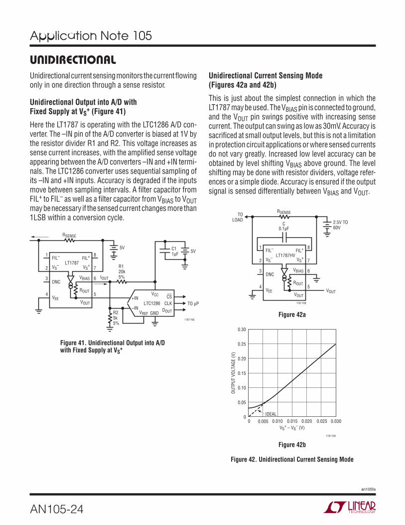
Unidirectional Output into A/D with Fixed Supply at VS
+ (Figure 41)
Here the LT1787 is operating with the LTC1286 A/D con-verter. The –IN pin of the A/D converter is biased at 1V by the resistor divider R1 and R2. This voltage increases as sense current increases, with the amplified sense voltage appearing between the A/D converters –IN and +IN termi-nals. The LTC1286 converter uses sequential sampling of its –IN and +IN inputs. Accuracy is degraded if the inputs move between sampling intervals. A filter capacitor from FIL+ to FIL– as well as a filter capacitor from VBIAS to VOUT may be necessary if the sensed current changes more than 1LSB within a conversion cycle.
Unidirectional Current Sensing Mode (Figures 42a and 42b)
This is just about the simplest connection in which the LT1787 may be used. The VBIAS pin is connected to ground, and the VOUT pin swings positive with increasing sense current. The output can swing as low as 30mV. Accuracy is sacrificed at small output levels, but this is not a limitation in protection circuit applications or where sensed currents do not vary greatly. Increased low level accuracy can be obtained by level shifting VBIAS above ground. The level shifting may be done with resistor dividers, voltage refer-ences or a simple diode. Accuracy is ensured if the output signal is sensed differentially between VBIAS and VOUT.
UNIDIRECTIONAL
R25k5%
1787 F06
IOUT
C11µF 5V
VREF
VCC
GND
LTC1286CS
CLKDOUT
+IN
–INTO µP
RSENSE
5V1
2
3
4
8
7
6
5
LT1787FIL+FIL–
VBIAS
VOUT
VS– VS
+
DNC
VEE
R120k5%
ROUT
Figure 41. Unidirectional Output into A/D with Fixed Supply at VS
+
Figure 42a
Figure 42b
1787 F08
C0.1µF
RSENSE
2.5V TO 60V
VOUT
TOLOAD
1
2
3
4
8
7
6
5
LT1787HVFIL+FIL–
VBIAS
VOUT
VS– VS
+
DNC
VEE
ROUT
VS+ – VS
– (V)0
OUTP
UT V
OLTA
GE (V
)
0.30
0.25
0.20
0.15
0.10
0.05
00.005 0.010
IDEAL0.015 0.020
1787 F09
0.025 0.030
Figure 42. Unidirectional Current Sensing Mode
Application Note 105
AN105-25
an105fa
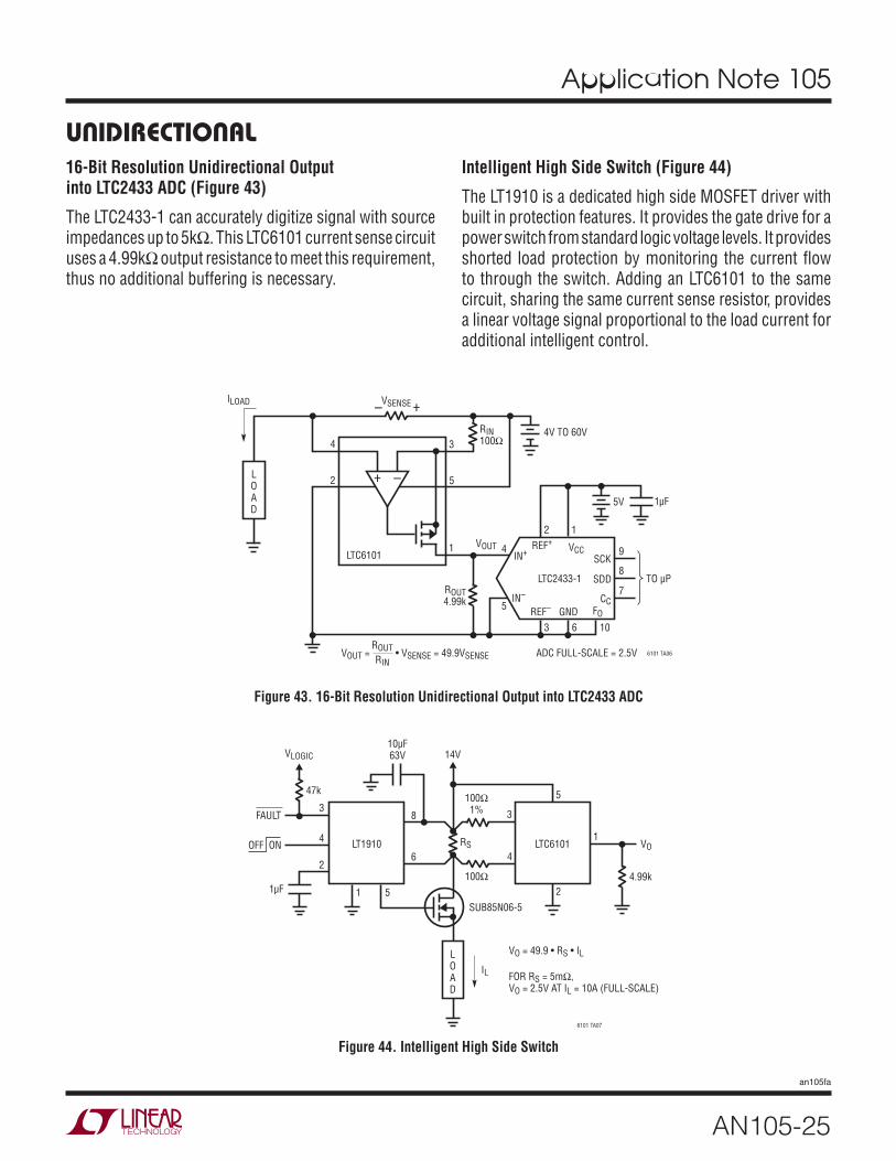
16-Bit Resolution Unidirectional Output into LTC2433 ADC (Figure 43)
The LTC2433-1 can accurately digitize signal with source impedances up to 5kΩ. This LTC6101 current sense circuit uses a 4.99kΩ output resistance to meet this requirement, thus no additional buffering is necessary.
UNIDIRECTIONAL
TO µP
6101 TA06
LTC2433-1
LTC6101
ROUT4.99k
RIN100Ω
VOUT
VSENSEILOAD
4V TO 60V
1µF5V
LOAD
–+
– +
VOUT = • VSENSE = 49.9VSENSEROUTRIN
ADC FULL-SCALE = 2.5V
2 1
9
8
7
1063
4
5
VCCSCK
REF+
REF– GND
IN+
IN– CCFO
SDD
52
1
34
6101 TA07
LOAD
FAULT
OFF ON
1 54.99k
VORS
3
4
47k
2
8
6
100Ω
100Ω1%
10µF63V
1µF
14VVLOGIC
SUB85N06-5
VO = 49.9 • RS • IL
FOR RS = 5mΩ,VO = 2.5V AT IL = 10A (FULL-SCALE)
LT1910 LTC6101
IL
5
2
1
3
4
Intelligent High Side Switch (Figure 44)
The LT1910 is a dedicated high side MOSFET driver with built in protection features. It provides the gate drive for a power switch from standard logic voltage levels. It provides shorted load protection by monitoring the current flow to through the switch. Adding an LTC6101 to the same circuit, sharing the same current sense resistor, provides a linear voltage signal proportional to the load current for additional intelligent control.
Figure 43. 16-Bit Resolution Unidirectional Output into LTC2433 ADC
Figure 44. Intelligent High Side Switch
Application Note 105
AN105-26
an105fa
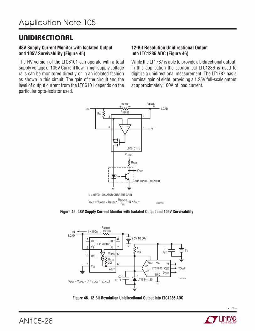
UNIDIRECTIONAL48V Supply Current Monitor with Isolated Output and 105V Survivability (Figure 45)
The HV version of the LTC6101 can operate with a total supply voltage of 105V. Current flow in high supply voltage rails can be monitored directly or in an isolated fashion as shown in this circuit. The gain of the circuit and the level of output current from the LTC6101 depends on the particular opto-isolator used.
12-Bit Resolution Unidirectional Output into LTC1286 ADC (Figure 46)
While the LT1787 is able to provide a bidirectional output, in this application the economical LTC1286 is used to digitize a unidirectional measurement. The LT1787 has a nominal gain of eight, providing a 1.25V full-scale output at approximately 100A of load current.
Figure 45. 48V Supply Current Monitor with Isolated Output and 105V Survivability
Figure 46. 12-Bit Resolution Unidirectional Output into LTC1286 ADC
6101 TA08
LTC6101HV
RIN
V–
V–
VSENSE
RSENSE
ISENSE
LOAD
+–
–+
VOUT = VLOGIC – ISENSE • • N • ROUTRSENSE
RIN
N = OPTO-ISOLATOR CURRENT GAIN
VS
ANY OPTO-ISOLATOR
ROUT
VOUT
VLOGIC
5 2
3 4
1 8
2 7
3 6
4 5
LT1787HV
RSENSE0.0016Ω
1787 TA01
C11µF 5V
FIL+FIL–
R115k
C20.1µFVOUT = VBIAS + (8 • ILOAD • RSENSE)
I = 100A
2.5V TO 60V
TOLOAD
LT1634-1.25
TO µP
VREF VCC
GND
LTC1286CS
CLKDOUT
+IN
–IN
VBIAS
VOUT
ROUT20k
VS– VS
+
DNC
VEE

Application Note 105
AN105-27
an105fa
UNIDIRECTIONAL
FIGURE TITLE20 Precision, Wide Dynamic Range High-side Current Sensing21 Sensed Current Includes Monitor Circuit Supply Current22 Wide Voltage Range Current Sensing23 Smooth Current Monitor Output Signal by Simple Filtering24 Power on Reset Pulse Using a TimerBlox Device25 Accurate Delayed Power on Reset Pulse Using TimerBlox Devices40 Monitor Current in Positive or Negative Supply Lines93 High Voltage Current and Temperature Monitoring104 Using Printed Circuit Sense Resistance105 High Voltage, 5A High Side Current Sensing in Small Package121 Single Output Provides 10A H-Bridge Current and Direction122 Monitor Solenoid Current on the Low Side123 Monitor Solenoid Current on the High Side125 Large Input Voltage Range for Fused Solenoid Current Monitoring126 Monitor both the ON Current and the Freewheeling Current Through a High Side Driven Solenoid127 Monitor both the ON Current and the Freewheeling Current In a Low Side Driven Solenoid129 Simple DC Motor Torque Control130 Small Motor Protection and Control131 Large Motor Protection and Control143 Battery Stack Monitoring148 Complete Single Cell Battery Protection167 Monitor Current in an Isolated Supply Line168 Monitoring a Fuse Protected Circuit169 Circuit Fault Protection with Early Warning and Latching Load Disconnect170 Use Comparator Output to Initialize Interrupt Routines171 Current Sense with Over-current Latch and Power-On Reset with Loss of Supply176 Directly Digitize Current with 16-Bit Resolution177 Directly Digitizing Two Independent Currents180 Complete Digital Current Monitoring182 Power Sensing with Built In A to D Converter183 Isolated Power Measurement184 Fast Data Rate Isolated Power Measurement185 Adding Temperature Measurement to Supply Power Measurement186 Current, Voltage and Fuse Monitoring187 Automotive Socket Power Monitoring188 Power over Ethernet, PoE, Monitoring189 Monitor Current, Voltage and Temperature208 Remote Current Sensing with Minimal Wiring
More Unidirectional Circuits Are Shown in Other Chapters:

Application Note 105
AN105-28
an105fa
UNIDIRECTIONALMore Unidirectional Circuits Are Shown in Other Chapters:
FIGURE TITLE210 Crystal/Reference Oven Controller211 Power Intensive Circuit Board Monitoring212 Crystal/Reference Oven Controller215 0A to 10A Sensing Over Two Ranges

Application Note 105
AN105-29
an105fa
Bidirectional current sensing monitors current flow in both directions through a sense resistor.
Bidirectional Current Sensing with Single-Ended Output (Figure 47)
Two LTC6101’s are used to monitor the current in a load in either direction. Using a separate rail-to-rail op amp to combine the two outputs provides a single ended output. With zero current flowing the output sits at the reference potential, one-half the supply voltage for maximum out-put swing or 2.5V as shown. With power supplied to the load through connection A the output will move positive between 2.5V and VCC. With connection B the output moves down between 2.5V and 0V.
Practical H-Bridge Current Monitor Offers Fault Detection and Bidirectional Load Information (Figure 48)
This circuit implements a differential load measurement for an ADC using twin unidirectional sense measurements. Each LTC6101 performs high side sensing that rapidly responds to fault conditions, including load shorts and MOSFET failures. Hardware local to the switch module (not shown in the diagram) can provide the protection logic and furnish a status flag to the control system. The two LTC6101 outputs taken differentially produce a bidirectional load measurement for the control servo. The ground-referenced signals are compatible with most ∆ΣADCs. The ∆ΣADC circuit also provides a “free” in-tegration function that removes PWM content from the measurement. This scheme also eliminates the need for analog-to-digital conversions at the rate needed to sup-port switch protection, thus reducing cost and complexity.
BIDIRECTIONAL
–
+
LOADB AB A
–
+
–
+
RS0.1
5V
VS
VOUT
2.5VREF
2.5k
2.5k
4 3 5
2 1 1 2
5 3
LTC6101 LTC6101
LT1490
I100Ω
100Ω
4
100Ω100Ω
2.5V TO 5V (CONNECTION A)2.5V TO 0V (CONNECTION B)0A TO 1A IN EITHER DIRECTION
+
IM
BATTERY BUS
DN374 F04
LTC6101
RS RS
RIN RINROUT
LTC6101ROUT
DIFFOUTPUTTO ADC
FOR IM RANGE = ±100A,DIFF OUT =±2.5V
RS = 1mΩRIN = 200ΩROUT = 4.99k
+
–
Figure 47. Bidirectional Current Sensing with Single-Ended Output
Figure 48. Practical H-Bridge Current Monitor Offers Fault Detection and Bidirectional Load Information

Application Note 105
AN105-30
an105fa
Conventional H-Bridge Current Monitor (Figure 49)
Many of the newer electric drive functions, such as steer-ing assist, are bidirectional in nature. These functions are generally driven by H-bridge MOSFET arrays using pulse-width modulation (PWM) methods to vary the commanded torque. In these systems, there are two main purposes for current monitoring. One is to monitor the current in the load, to track its performance against the desired com-mand (i.e., closed-loop servo law), and another is for fault detection and protection features.
A common monitoring approach in these systems is to amplify the voltage on a “flying” sense resistor, as shown. Unfortunately, several potentially hazardous fault scenarios go undetected, such as a simple short to ground at a motor terminal. Another complication is the noise introduced by the PWM activity. While the PWM noise may be filtered for purposes of the servo law, information useful for protection becomes obscured. The best solution is to simply provide two circuits that individually protect each half-bridge and report the bidirectional load current. In some cases, a smart MOSFET bridge driver may already include sense resistors and offer the protection features needed. In these situations, the best solution is the one that derives the load information with the least additional circuitry.
Single-Supply 2.5V Bidirectional Operation with External Voltage Reference and I/V Converter (Figure 50)
The LT1787’s output is buffered by an LT1495 rail-to-rail op amp configured as an I/V converter. This configuration is ideal for monitoring very low voltage supplies. The LT1787’s VOUT pin is held equal to the reference voltage appearing at the op amp’s noninverting input. This al-lows one to monitor supply voltages as low as 2.5V. The op amp’s output may swing from ground to its positive supply voltage. The low impedance output of the op amp may drive following circuitry more effectively than the high output impedance of the LT1787. The I/V converter configuration also works well with split supply voltages.
BIDIRECTIONAL
Figure 49. Conventional H-Bridge Current Monitor
Figure 50. Single-Supply 2.5V Bidirectional Operation with External Voltage Reference and I/V Converter
–
+
+
IM
RS
BATTERY BUS
DIFFAMP
DN374 F03
2.5V
C11µF
RSENSEISENSE
2.5V + VSENSE(MAX)
TOCHARGER/
LOAD
VOUT A
1M5%
1787 F07
LT1495
C31000pF
LT1389-1.25
2.5V +
–A1
1
2
3
4
8
7
6
5
LT1787FIL+FIL–
VBIAS
VOUT
VS– VS
+
DNC
VEE
ROUT

Application Note 105
AN105-31
an105fa
BIDIRECTIONAL
–
+
–
+
1495 TA05
RSENSE0.1Ω
ILCHARGE
RA
2N3904
VO = IL RSENSE
FOR RA = 1k, RB = 10k
= 1V/A
CHARGEOUT
DISCHARGEOUT
DISCHARGE
2N3904
RA
RA RA
RB
RBRA
VOIL
RB
A11/2 LT1495
5V 12V
A21/2 LT1495
( )
Battery Current Monitor (Figure 51)
One LT1495 dual op amp package can be used to establish separate charge and discharge current monitoring outputs. The LT1495 features Over-the-Top operation allowing the battery potential to be as high as 36V with only a 5V amplifier supply voltage.
LT1995G = 1
SENSEOUTPUT100mV/A
FLAGOUTPUT4A LIMIT
15V15V TO –15V
0.1Ω
I
10k
1995 TA05
10kLT6700-3
–
+
400mV
–15V
REF
P1
M1
Fast Current Sense with Alarm (Figure 52)
The LT1995 is shown as a simple unity gain difference amplifier. When biased with split supplies the input current can flow in either direction providing an output voltage of 100mV per Amp from the voltage across the 100mΩ sense resistor. With 32MHz of bandwidth and 1000V/µs slew rate the response of this sense amplifier is fast. Adding a simple comparator with a built in reference voltage circuit such as the LT6700-3 can be used to generate an overcur-rent flag. With the 400mV reference the flag occurs at 4A.
Figure 51. Battery Current Monitor
Figure 52. Fast Current Sense with Alarm

Application Note 105
AN105-32
an105fa
BIDIRECTIONAL
LOAD
CHARGER
–+ – +
+
–
+
–
VOUT D = IDISCHARGE • RSENSE ( ) WHEN IDISCHARGE ≥ 0DISCHARGING:ROUT DRIN D
VOUT C = ICHARGE • RSENSE ( ) WHEN ICHARGE ≥ 0CHARGING:ROUT CRIN C
6101 TA02
VBATT2
4
RIN C100
1
5
3
LTC6101
RIN D100
5
1
3
RIN C100
LTC6101
VOUT DROUT D
4.99kROUT C4.99k
VOUT C
2
4
RIN D100
IDISCHARGE RSENSE ICHARGE
Bidirectional Current Sense with Separate Charge/Discharge Output (Figure 53)
In this circuit the outputs are enabled by the direction of current flow. The battery current when either charging or discharging enables only one of the outputs. For ex-ample when charging, the VOUT D signal goes low since the output MOSFET of that LTC6101 turns completely off while the other LT6101, VOUT C, ramps from low to high in proportion to the charging current. The active output reverses when the charger is removed and the battery discharges into the load.
Figure 53. Bidirectional Current Sense with Separate Charge/Discharge Output
Figure 54. Bidirectional Absolute Value Current Sense
Bidirectional Absolute Value Current Sense (Figure 54)
The high impedance current source outputs of two LTC6101’s can be directly tied together. In this circuit the voltage at VOUT continuously represents the absolute value of the magnitude of the current into or out of the battery. The direction or polarity of the current flow is not discriminated.
LOAD
CHARGER
–+ – +
+
–
VOUT = IDISCHARGE • RSENSE ( ) WHEN IDISCHARGE ≥ 0DISCHARGING:ROUTRIN D
VOUT = ICHARGE • RSENSE ( ) WHEN ICHARGE ≥ 0CHARGING:ROUTRIN C
6101 TA05
VBATT2
4
RIN C
1
5
3
LTC6101
RIN D
5
1
3
RIN C
LTC6101
ROUTVOUT
2
4
RIN D
IDISCHARGE ICHARGERSENSE

Application Note 105
AN105-33
an105fa
BIDIRECTIONALFull-Bridge Load Current Monitor (Figure 55)
The LT1990 is a difference amplifier that features a very wide common mode input voltage range that can far exceed its own supply voltage. This is an advantage to reject transient voltages when used to monitor the current in a full-bridge driven inductive load such as a motor. The LT6650 provides a voltage reference of 1.5V to bias up the output away from ground. The output will move above or below 1.5V as a function of which direction the current in the load is flowing. As shown, the amplifier provides a gain of 10 to the voltage developed across resistor RS.
Low Power, Bidirectional 60V Precision High Side Current Sense (Figure 56)
Using a very precise zero-drift amplifier as a pre-amp allows for the use of a very small sense resistor in a high voltage supply line. A floating power supply regulates the voltage across the pre-amplifier on any voltage rail up to the 60V limit of the LT1787HV circuit. Overall gain of this circuit is 1000. A 1mA change in current in either direction through the 10mΩ sense resistor will produce a 10mV change in the output voltage.
RS
+VSOURCE
IL
–12V ≤ VCM ≤ 73VVOUT = VREF ± (10 • IL • RS)
–
+
40k40k 100k
100k
900k
1M
1M
900k 10k
10k
VOUT
LT1990
LT6650 GND
IN OUT
FB
54.9k
20k
1nF
1µF
VREF = 1.5V
1990 TA01
5V
7
2
3
4
1
8
6
5
+–
–
+
LT1787HV
VS– VS
+
4.7µF
VOUT = 2.5V +1000* VSENSE
2.5V REF
1
5 3
53
1
164
4
2
2
8
5
6
72
4
PRECISIONBIDIRECTIONALHIGH VOLTAGELEVEL SHIFT
AND GAIN OF 8
0.1µF
10µF10µF 1µF0.1µF100Ω
LTC2054
BAT54
LTC1754-51N4686
3.9VZ
33Ω
2N5401
MPSA42
– +VSENSE
POSITIVE SENSE
10mΩ
PRECISION BIDIRECTIONAL
GAIN OF 125
12.4k
POWER SUPPLY(NOTE: POSITIVE CURRENT SENSE
INCLUDES CIRCUITSUPPLY CURRENT)
20545 TA06
35.7k
ON 5VOFF 0V
100Ω
Figure 55. Full-Bridge Load Current Monitor
Figure 56. Low Power, Bidirectional 60V Precision High Side Current Sense

Application Note 105
AN105-34
an105fa
BIDIRECTIONAL
Figure 57. Split or Single Supply Operation, Bidirectional Output into A/D
Figure 58. Bidirectional Precision Current Sensing
Split or Single Supply Operation, Bidirectional Output into A/D (Figure 57)
In this circuit, split supply operation is used on both the LT1787 and LT1404 to provide a symmetric bidirectional measurement. In the single-supply case, where the LT1787 Pin 6 is driven by VREF, the bidirectional measurement range is slightly asymmetric due to VREF being somewhat greater than midspan of the ADC input range.
Bidirectional Precision Current Sensing (Figure 58)
This circuit uses two LTC6102 devices, one for each di-rection of current flow through a single sense resistance. While each output only provides a result in one particular direction of current, taking the two output signals differ-entially provides a bipolar signal to other circuitry such as an ADC. Since each circuit has its own gain resistors, bilinear scaling is possible (different scaling depending on direction).
1Ω1%
VEE–5V
VOUT (±1V)
VSRCE≈4.75V
IS = ±125mA
1
2
3
4
8
7
6
5
LT1787FIL+FIL–
VBIAS
VOUT
VS– VS
+
DNC
VEE
20k
1787 TA02
10µF16V
7
6
8
5
4
3
2
1
VREFGND
LTC1404
CONV
CLK
DOUT
AIN
VCC5V
VEE–5V
DOUT
OPTIONAL SINGLESUPPLY OPERATION:
DISCONNECT VBIASFROM GROUND
AND CONNECT IT TO VREF.REPLACE –5V SUPPLY
WITH GROUND.OUTPUT CODE FOR ZEROCURRENT WILL BE ~2430
10µF16V
10µF16V
CLOCKINGCIRCUITRY
CHARGER
–+ – +
+
–
+
–
LOAD
VOUT D = IDISCHARGE • RSENSE ( ) WHEN IDISCHARGE ≥ 0DISCHARGING:ROUT DRIN D
VOUT C = ICHARGE • RSENSE ( ) WHEN ICHARGE ≥ 0CHARGING:ROUT CRIN C
6102 TA02
VBATT
RIN D100Ω
LTC6102
RIN C100Ω
RIN D100Ω
LTC6102
VOUT CROUT C
4.99kROUT D4.99k
VOUT D
RIN C100Ω
ICHARGE RSENSE IDISCHARGE
V+V–
OUT
–INS+IN
V+ V–
OUT
–INS +IN
–INF –INF
VREG0.1µF
VREG0.1µF

Application Note 105
AN105-35
an105fa
Differential Output Bidirectional 10A Current Sense (Figure 59)
The LTC6103 has dual sense amplifiers and each measures current in one direction through a single sense resistance. The outputs can be taken together as a differential output to subsequent circuitry such as an ADC. Values shown are for 10A maximum measurement.
Absolute Value Output Bidirectional Current Sensing (Figure 60)
Connecting an LTC6103 so that the outputs each represent opposite current flow through a shared sense resistance, but with the outputs driving a common load, results in a positive only output function while sensing bidirectionally.
BIDIRECTIONAL
+200ΩVBATT
6103 TA02
DIFFERENTIAL OUTPUT*±2.5V FS (+ IS CHARGE CURRENT)
OUTPUT SWING MAY BE LIMITED FORVBATT BELOW 6V
+–
200Ω
4.99k
4V < VBATT < 60V
+OUTPUT MAY BE TAKEN SINGLE ENDED AS CHARGE CURRENT MONITOR–OUTPUT MAY BE TAKEN SINGLE ENDED AS DISCHARGE CURRENT MONITOR
*
CHARGERLOAD
10mΩ
+ – +–
8 7 6 5
241
+INA
OUTA OUTB
VSBVSA
LTC6103
–INA –INB +INB
V–
4.99k
+
20mΩ
VBATT
6103 TA03
200Ω200Ω
4.99k
VOUT2.5V FS
CHARGERLOAD
+ – +–
8 7 6 5
241
+INA
OUTA OUTB
VSBVSA
LTC6103
–INA –INB +INB
V–
Figure 59. Differential Output Bidirectional 10A Current Sense
Figure 60. Absolute Value Output Bidirectional Current Sensing

Application Note 105
AN105-36
an105fa
BIDIRECTIONALMore Bidirectional Circuits Are Shown in Other Chapters:
FIGURE TITLE104 Using Printed Circuit Sense Resistance120 Bidirectional Current Sensing in H-Bridge Drivers124 Monitor H-Bridge Motor Current Directly128 Fixed Gain DC Motor Current Monitor136 Coulomb Counting Battery Gas Gauge142 Monitor Charge and Discharge Currents at One Output145 High Voltage Battery Coulomb Counting146 Low Voltage Battery Coulomb Counting147 Single Cell Lithium-Ion Battery Coulomb Counter178 Digitize a Bidirectional Current Using a Single Sense Amplifier and ADC179 Digitizing Charging and Loading Current in a Battery Monitor181 Ampere-Hour Gauge209 Use Kelvin Connections to Maintain High Current Accuracy216 Dual Sense Amplifier Can Have Different Sense Resistors and Gain

Application Note 105
AN105-37
an105fa
Sensing current in AC power lines is quite tricky in the sense that both the current and voltage are continuously changing polarity. Transformer coupling of signals to drive ground referenced circuitry is often a good approach.
Single-Supply RMS Current Measurement (Figure 61)
The LT1966 is a true RMS-to-DC converter that takes a single-ended or differential input signal with rail-to-rail range. The output of a PCB mounted current sense trans-
ACformer can be connected directly to the converter. Up to 75A of AC current is measurable without breaking the signal path from a power source to a load. The accurate operating range of the circuit is determined by the selection of the transformer termination resistor. All of the math is built in to the LTC1966 to provide a DC output voltage that is proportional to the true RMS value of the current. This is valuable in determining the power/energy consumption of AC-powered appliances.
V+
LTC1966IN1
VOUT = 4mVDC/ARMSCAVE1µF
0.1µF
IN2
1966 TA08
VOUTAC CURRENT
75A MAX50Hz TO 400Hz
OUT RTN
GND ENVSS100k
100k
10Ω
T1: CR MAGNETICS CR8348-2500-N www.crmagnetics.com
T1
Figure 61. Single-Supply RMS Current Measurement
More AC Circuits Are Shown in Other Chapters:FIGURE TITLE
120 Bidirectional Current Sensing in H-Bridge Drivers124 Monitor H-Bridge Motor Current Directly128 Fixed Gain DC Motor Current Monitor

Application Note 105
AN105-38
an105fa
DC current sensing is for measuring current flow that is changing at a very slow rate.
Micro-Hotplate Voltage and Current Monitor (Figure 62)
Materials science research examines the properties and interactions of materials at various temperatures. Some of the more interesting properties can be excited with localized nano-technology heaters and detected using the presence of interactive thin films.
While the exact methods of detection are highly complex and relatively proprietary, the method of creating localized heat is as old as the light bulb. Shown is the schematic of the heater elements of a Micro-hotplate from Boston Microsystems (www.bostonmicrosystems.com). The physical dimensions of the elements are tens of microns. They are micromachined out of SiC and heated with simple DC electrical power, being able to reach 1000°C without damage.
The power introduced to the elements, and thereby their temperature, is ascertained from the voltage-current product with the LT6100 measuring the current and the
LT1991 measuring the voltage. The LT6100 senses the current by measuring the voltage across the 10Ω resistor, applies a gain of 50, and provides a ground referenced output. The I to V gain is therefore 500mV/mA, which makes sense given the 10mA full-scale heater current and the 5V output swing of the LT6100. The LT1991’s task is the opposite, applying precision attenuation instead of gain. The full-scale voltage of the heater is a total of 40V (±20), beyond which the life of the heater may be reduced in some atmospheres. The LT1991 is set up for an attenua-tion factor of 10, so that the 40V full-scale differential drive becomes 4V ground referenced at the LT1991 output. In both cases, the voltages are easily read by 0V–5V PC I/O cards and the system readily software controlled.
Battery Current Monitor (Figure 63)
One LT1495 dual op amp package can be used to estab-lish separate charge and discharge current monitoring outputs. The LT1495 features Over-the-Top operation allowing the battery potential to be as high as 36V with only a 5V amplifier supply voltage.
DC
MICRO-HOTPLATEBOSTON
MICROSYSTEMSMHP100S-005
IHOTPLATE
M9
LT1991
5V
6100 TA06
5V
M3M1P1P3P9
10Ω1%
+–
VS–
VEE
VCC
A2LT6100
5V CURRENTMONITORVOUT = 500mV/mA
VOLTAGEMONITOR
VOUT =
www.bostonmicrosystems.com
VDR+
VDR–
A4
VS+
VDR+ – VDR
–
10
–
+
–
+
1495 TA05
RSENSE0.1Ω
ILCHARGE
RA
2N3904
VO = IL RSENSE
FOR RA = 1k, RB = 10k
= 1V/A
CHARGEOUT
DISCHARGEOUT
DISCHARGE
2N3904
RA
RA RA
RB
RBRA
VOIL
RB
A11/2 LT1495
5V 12V
A21/2 LT1495
( )
Figure 62. Micro-Hotplate Voltage and Current Monitor
Figure 63. Battery Current Monitor

Application Note 105
AN105-39
an105fa
Bidirectional Battery-Current Monitor (Figure 64)
This circuit provides the capability of monitoring current in either direction through the sense resistor. To allow negative outputs to represent charging current, VEE is connected to a small negative supply. In single-supply operation (VEE at ground), the output range may be offset upwards by applying a positive reference level to VBIAS (1.25V for example). C3 may be used to form a filter in conjunction with the output resistance (ROUT) of the part. This solution offers excellent precision (very low VOS) and a fixed nominal gain of 8.
VOS performance of op amps at the supply is generally not factory trimmed, thus less accurate than other solutions. The finite current gain of the bipolar transistor is a small source of gain error.
High Side Current Sense and Fuse Monitor (Figure 66)
The LT6100 can be used as a combination current sen-sor and fuse monitor. This part includes on-chip output buffering and was designed to operate with the low supply voltage (≥2.7V), typical of vehicle data acquisition systems, while the sense inputs monitor signals at the higher bat-tery bus potential. The LT6100 inputs are tolerant of large input differentials, thus allowing the blown-fuse operating condition (this would be detected by an output full-scale indication). The LT6100 can also be powered down while maintaining high impedance sense inputs, drawing less than 1µA max from the battery bus.
DC
*OPTIONAL
C21µF–5V
1787 F02
OUTPUT
C3*1000pF
C11µF
RSENSE
15V
TOCHARGER/
LOAD
1
2
3
4
8
7
6
5
LT1787FIL+FIL–
VBIAS
VOUT
VS– VS
+
DNC
VEE
ROUT
Figure 64. Bidirectional Battery-Current Monitor
Figure 66. High Side Current Sense and Fuse Monitor
Figure 65. “Classic” Positive Supply Rail Current Sense
“Classic” Positive Supply Rail Current Sense (Figure 65)
This circuit uses generic devices to assemble a function similar to an LTC6101. A rail-to-rail input type op amp is required since input voltages are right at the upper rail. The circuit shown here is capable of monitoring up to 44V applications. Besides the complication of extra parts, the
–
+LT1637
5V
200Ω
200Ω
0.2Ω
2k
0V TO 4.3V
1637 TA02VOUT = (2Ω)(ILOAD)
Q12N3904
LOAD ILOAD
OUTPUT2.5V = 25AVEE
OUT
DN374 F02
RSENSE2mΩ FUSE
LT6100
81
VS– VS
+
BATTERYBUS
A4ADC
POWER≥2.7V
2VCC
A23
4
7
C20.1µF
6
5
FIL
TO LOAD
– +
+

Application Note 105
AN105-40
an105fa
Gain of 50 Current Sense (Figure 67)
The LT6100 is configured for a gain of 50 by grounding both A2 and A4. This is one of the simplest current sensing amplifier circuits where only a sense resistor is required.
Dual LTC6101’s Allow High-Low Current Ranging (Figure 68)
Using two current sense amplifiers with two values of sense resistors is an easy method of sensing current over a wide range. In this circuit the sensitivity and resolution of measurement is 10 times greater with low currents, less than 1.2A, than with higher currents. A comparator detects higher current flow, up to 10A, and switches sensing over to the high current circuitry.
DC
VOUT50 • RSENSE • ISENSE
FIL
VCC
6100 TA04
RSENSE
LT6100 VS–VS
+
VEE A2 A4
5V
VSUPPLY6.4V TO 48V
ISENSE
–+
LOAD
Figure 67. Gain of 50 Current Sense
Figure 68. Dual LTC6101’s Allow High-Low Current Ranging
6101 F03b
–+ –+
–+
R57.5k
VIN
301301
VOUT
ILOAD
5
1
3
LTC6101
2
4
RSENSE LO100m
M1Si4465
10k
CMPZ4697
7.5k
VIN
1.74M4.7k
Q1CMPT5551
40.2k
3
4
5
6
12
8
7
619k
HIGHRANGE
INDICATOR(ILOAD > 1.2A)
VLOGIC(3.3V TO 5V)
LOW CURRENT RANGE OUT2.5V/A
(VLOGIC +5V) ≤ VIN ≤ 60V
0 ≤ ILOAD ≤ 10A
HIGH CURRENT RANGE OUT250mV/A
301 301
5
1
3
LTC6101
2
4
RSENSE HI10m
VLOGIC
BAT54C
LTC1540

Application Note 105
AN105-41
an105fa
power to the circuit with batteries, any voltage potential at the inputs are handled. The LT1495 is a micropower op amp so the quiescent current drain from the batteries is very low and thus no on/off switch is required.
Two Terminal Current Regulator (Figure 69)
The LT1635 combines an op amp with a 200mV reference. Scaling this reference voltage to a potential across resistor R3 forces a controlled amount of current to flow from the +terminal to the –terminal. Power is taken from the loop.
DC
8
3
1635 TA05
2
14
7
6
+
–
R1
R2
–
+LT1635
(R2 + R3)VREF(R1)(R3)
IOUT =
R3
Figure 69. Two Terminal Current Regulator
Figure 70. High Side Power Supply Current Sense
Figure 71. 0nA to 200nA Current Meter
Figure 72. Over-The-Top Current Sense
High Side Power Supply Current Sense (Figure 70)
The low offset error of the LTC6800 allows for unusually low sense resistance while retaining accuracy.
–
+LTC6800
45
6
7OUT100mV/AOF LOADCURRENT10k
1.5mΩ
0.1µF
150Ω
6800 TA01
ILOAD
82
VREGULATOR
3
LOAD
–
+
–
+
µA
1495 TA06
1/2LT1495
1/2LT1495
100pF
R110M
R29k
1.5V
1.5V
R32kFULL-SCALEADJUST
IS = 3µA WHEN IIN = 0NO ON/OFF SWITCH REQUIRED
0µA TO200µA
R410k
INPUTCURRENT
Over-The-Top Current Sense (Figure 72)
This circuit is a variation on the “classic” high side cir-cuit, but takes advantage of Over-the-Top input capability to separately supply the IC from a low voltage rail. This provides a measure of fault protection to downstream circuitry by virtue of the limited output swing set by the low voltage supply. The disadvantage is VOS in the Over-the-Top mode is generally inferior to other modes, thus less accurate. The finite current gain of the bipolar transistor is a source of small gain error.
–
+LT1637
3V TO 44V
3V
R1200Ω
RS0.2Ω
R22k
VOUT(0V TO 2.7V)
Q12N3904
1637 TA06
LOAD
ILOAD
VOUT(RS)(R2/R1)
ILOAD =
0nA to 200nA Current Meter (Figure 71)
A floating amplifier circuit converts a full-scale 200nA flowing in the direction indicated at the inputs to 2V at the output of the LT1495. This voltage is converted to a current to drive a 200µA meter movement. By floating the

Application Note 105
AN105-42
an105fa
DCConventional H-Bridge Current Monitor (Figure 73)
Many of the newer electric drive functions, such as steer-ing assist, are bidirectional in nature. These functions are generally driven by H-bridge MOSFET arrays using pulse-width modulation (PWM) methods to vary the commanded torque. In these systems, there are two main purposes for current monitoring. One is to monitor the current in the load, to track its performance against the desired com-mand (i.e., closed-loop servo law), and another is for fault detection and protection features.
A common monitoring approach in these systems is to amplify the voltage on a “flying” sense resistor, as shown. Unfortunately, several potentially hazardous fault scenarios go undetected, such as a simple short to ground at a motor terminal. Another complication is the noise introduced by the PWM activity. While the PWM noise may be filtered for purposes of the servo law, information useful for protection becomes obscured. The best solution is to simply provide two circuits that individually protect each half-bridge and report the bidirectional load current. In some cases, a smart MOSFET bridge driver may already include sense resistors and offer the protection features needed. In these situations, the best solution is the one that derives the load information with the least additional circuitry.
–
+
+
IM
RS
BATTERY BUS
DIFFAMP
DN374 F03
Figure 73. Conventional H-Bridge Current Monitor
Figure 74. Single-Supply 2.5V Bidirectional Operation with External Voltage Reference and I/V Converter
Single-Supply 2.5V Bidirectional Operation with External Voltage Reference and I/V Converter (Figure 74)
The LT1787’s output is buffered by an LT1495 rail-to-rail op amp configured as an I/V converter. This configuration is ideal for monitoring very low voltage supplies. The LT1787’s VOUT pin is held equal to the reference voltage appearing at the op amp’s non-inverting input. This al-lows one to monitor supply voltages as low as 2.5V. The op amp’s output may swing from ground to its positive supply voltage. The low impedance output of the op amp may drive following circuitry more effectively than the high output impedance of the LT1787. The I/V converter configuration also works well with split supply voltages.
2.5V
C11µF
RSENSEISENSE
2.5V + VSENSE(MAX)
TOCHARGER/
LOAD
VOUT A
1M5%
1787 F07
LT1495
C31000pF
LT1389-1.25
2.5V +
–A1
1
2
3
4
8
7
6
5
LT1787FIL+FIL–
VBIAS
VOUT
VS– VS
+
DNC
VEE
ROUT
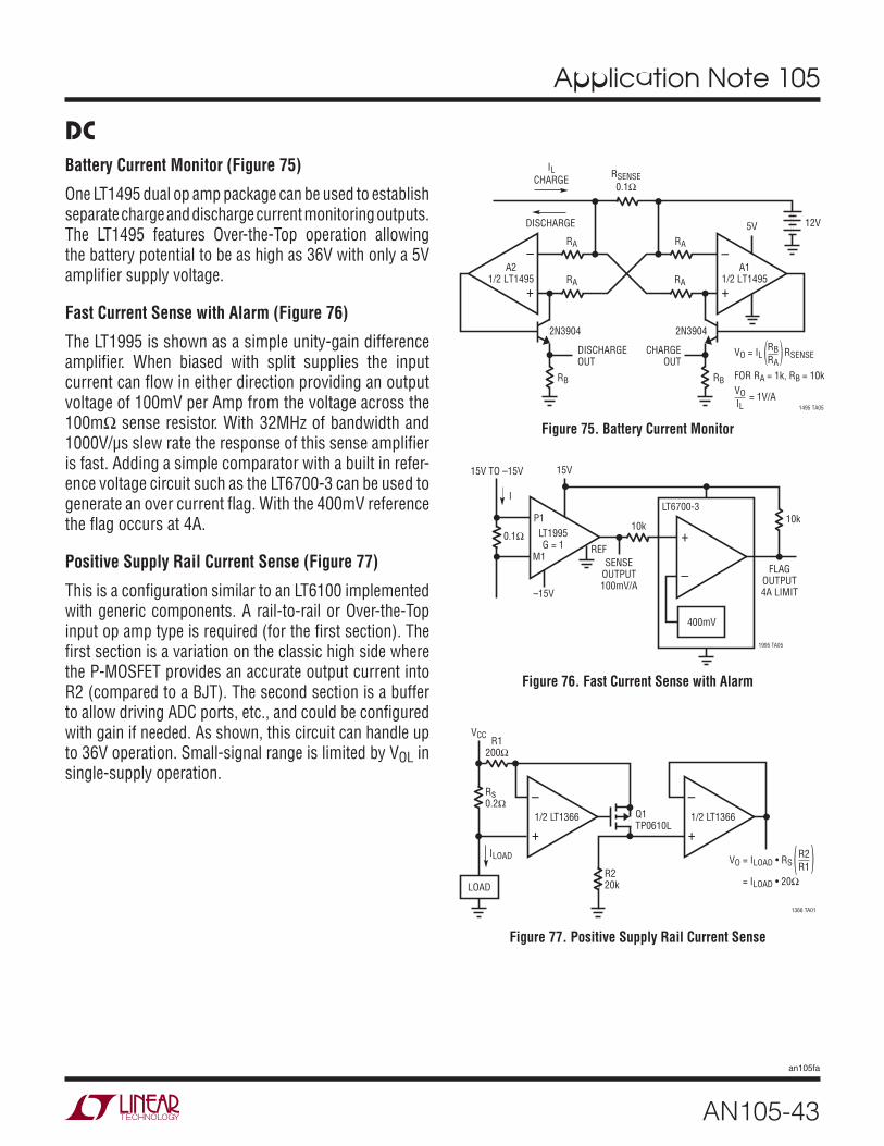
Application Note 105
AN105-43
an105fa
DC
Figure 75. Battery Current Monitor
Figure 76. Fast Current Sense with Alarm
Figure 77. Positive Supply Rail Current Sense
–
+
–
+
1495 TA05
RSENSE0.1Ω
ILCHARGE
RA
2N3904
VO = IL RSENSE
FOR RA = 1k, RB = 10k
= 1V/A
CHARGEOUT
DISCHARGEOUT
DISCHARGE
2N3904
RA
RA RA
RB
RBRA
VOIL
RB
A11/2 LT1495
5V 12V
A21/2 LT1495
( )
Battery Current Monitor (Figure 75)
One LT1495 dual op amp package can be used to establish separate charge and discharge current monitoring outputs. The LT1495 features Over-the-Top operation allowing the battery potential to be as high as 36V with only a 5V amplifier supply voltage.
Fast Current Sense with Alarm (Figure 76)
The LT1995 is shown as a simple unity-gain difference amplifier. When biased with split supplies the input current can flow in either direction providing an output voltage of 100mV per Amp from the voltage across the 100mΩ sense resistor. With 32MHz of bandwidth and 1000V/µs slew rate the response of this sense amplifier is fast. Adding a simple comparator with a built in refer-ence voltage circuit such as the LT6700-3 can be used to generate an over current flag. With the 400mV reference the flag occurs at 4A.
Positive Supply Rail Current Sense (Figure 77)
This is a configuration similar to an LT6100 implemented with generic components. A rail-to-rail or Over-the-Top input op amp type is required (for the first section). The first section is a variation on the classic high side where the P-MOSFET provides an accurate output current into R2 (compared to a BJT). The second section is a buffer to allow driving ADC ports, etc., and could be configured with gain if needed. As shown, this circuit can handle up to 36V operation. Small-signal range is limited by VOL in single-supply operation.
LT1995G = 1
SENSEOUTPUT100mV/A
FLAGOUTPUT4A LIMIT
15V15V TO –15V
0.1Ω
I
10k
1995 TA05
10kLT6700-3
–
+
400mV
–15V
REF
P1
M1
–
+1/2 LT1366
R1200Ω
1366 TA01
LOAD
ILOAD
Rs0.2Ω
R220k
Q1TP0610L
VCC
VO = ILOAD • RS
= ILOAD • 20Ω
( )
–
+1/2 LT1366
R2R1

Application Note 105
AN105-44
an105fa
DCLT6100 Load Current Monitor (Figure 78)
This is the basic LT6100 circuit configuration. The internal circuitry, including an output buffer, typically operates from a low voltage supply, such as the 3V shown. The moni-tored supply can range anywhere from VCC + 1.4V up to 48V. The A2 and A4 pins can be strapped various ways to provide a wide range of internally fixed gains. The input leads become very Hi-Z when VCC is powered down, so as not to drain batteries for example. Access to an internal signal node (Pin 3) provides an option to include a filtering function with one added capacitor. Small-signal range is limited by VOL in single-supply operation.
1A Voltage-Controlled Current Sink (Figure 79)
This is a simple controlled current sink, where the op amp drives the N-MOSFET gate to develop a match between the 1Ω sense resistor drop and the VIN current command. Since the common mode voltage seen by the op amp is near ground potential, a “single-supply” or rail-to-rail type is required in this application.
LTC6101 Supply Current Included as Load in Measurement (Figure 80)
This is the basic LTC6101 high side sensing supply-monitor configuration, where the supply current drawn by the IC is included in the readout signal. This configuration is use-ful when the IC current may not be negligible in terms of overall current draw, such as in low power battery-powered applications. RSENSE should be selected to limit voltage drop to <500mV for best linearity. If it is desirable not to include the IC current in the readout, as in load monitor-ing, Pin 5 may be connected directly to V+ instead of the load. Gain accuracy of this circuit is limited only by the precision of the resistors selected by the user.
–
+VIN
V+
1/2LT1492
RL
IOUT
1492/93 TA06
1k
100Ω
100pF
Si9410DYN-CHANNEL
1Ω
V+
IOUT = VIN1Ω
tr < 1µs
Figure 79. 1A Voltage-Controlled Current Sink
Figure 80. LTC6101 Supply Current Included as Load in Measurement
LTC6101ROUT
VOUT
6101 F06
RIN
LOAD
V+
RSENSE
–+
52
1
34
Figure 78. LT6100 Load Current Monitor
OUTPUTVEEOUT
6100 F04
RSENSE
LT6100
81
VS– VS
+
A42
VCC
A23
4
7
C20.1µF
C10.1µF
3V
6
5
FIL
TO LOAD
+
5V+
– +

Application Note 105
AN105-45
an105fa
V+ Powered Separately from Load Supply (Figure 81)
The inputs of the LTC6101 can function from 1.4V above the device positive supply to 48V DC. In this circuit the current flow in the high voltage rail is directly translated to a 0V to 3V range.
Simple High Side Current Sense Using the LTC6101 (Figure 82)
This is a basic high side current monitor using the LTC6101. The selection of RIN and ROUT establishes the desired gain of this circuit, powered directly from the battery bus. The current output of the LTC6101 allows it to be located re-motely to ROUT. Thus, the amplifier can be placed directly at the shunt, while ROUT is placed near the monitoring electronics without ground drop errors. This circuit has a fast 1µs response time that makes it ideal for providing MOSFET load switch protection. The switch element may be the high side type connected between the sense resistor and the load, a low side type between the load and ground or an H-bridge. The circuit is programmable to produce up to 1mA of full-scale output current into ROUT, yet draws a mere 250µA supply current when the load is off.
“Classic” High Precision Low Side Current Sense (Figure 83)
This configuration is basically a standard noninverting amplifier. The op amp used must support common mode operation at the lower rail and the use of a zero-drift type (as shown) provides excellent precision. The output of this circuit is referenced to the lower Kelvin contact, which could be ground in a single-supply application. Small-signal range is limited by VOL for single-supply designs. Scaling accuracy is set by the quality of the user-selected resistors.
DC
Figure 81. V+ Powered Separately from Load Supply
Figure 82. Simple High Side Current Sense Using the LTC6101
Figure 83. “Classic” High Precision Low Side Current Sense
VEE
VOUT
4
FIL
A4VCC
VS+
RSENSE3mΩ
8
VS–
1
3V
CONFIGURED FOR GAIN = 25V/V
4.4V TO 48VSUPPLY
A2
72 6
LT6100
3
5
6100 TA01a
VOUT = 2.5VISENSE = 33A
220pF
LOAD
DN374 F01
LT6101
4
LOAD
BATTERY BUS
RSENSE0.01Ω
RIN100Ω
2
3
5
1 VOUT4.99V = 10A
VOUT = ILOAD(RSENSE • ROUT/RIN)
ROUT4.99k
–+
–
+LTC2050HV
1
4
3
2050 TA08
5
2
5V
–5V
TOMEASURED
CIRCUIT
OUT 3V/AMPLOAD CURRENTIN MEASUREDCIRCUIT, REFERRED TO –5V
10Ω 10k
3mΩ
0.1µFLOAD CURRENT

Application Note 105
AN105-46
an105fa
DCMore DC Circuits Are Shown in Other Chapters:
FIGURE TITLE20 Precision, Wide Dynamic Range High-side Current Sensing22 Wide Voltage Range Current Sensing58 Bidirectional Precision Current Sensing59 Differential Output Bidirectional 10A Current Sense60 Absolute Value Output Bidirectional Current Sensing142 Monitor Charge and Discharge Currents at One Output178 Digitize a Bi-Directional Current Using a Single Sense Amplifier and ADC208 Remote Current Sensing with Minimal Wiring209 Use Kelvin Connections to Maintain High Current Accuracy216 Dual Sense Amplifier Can Have Different Sense Resistors and Gain

Application Note 105
AN105-47
an105fa
Quite often it is required to sense current flow in a sup-ply rail that is a much higher voltage potential than the supply voltage for the system electronics. Current sense circuits with high voltage capability are useful to translate information to lower voltage signals for processing.
Over-The-Top Current Sense (Figure 84)
This circuit is a variation on the “classic” high side cir-cuit, but takes advantage of Over-the-Top input capability to separately supply the IC from a low voltage rail. This provides a measure of fault protection to downstream circuitry by virtue of the limited output swing set by the low voltage supply. The disadvantage is VOS in the Over-the-Top mode is generally inferior to other modes, thus less accurate. The finite current gain of the bipolar transistor is a source of small gain error.
LEVEL SHIFTING
–
+LT1637
3V TO 44V
3V
R1200Ω
RS0.2Ω
R22k
VOUT(0V TO 2.7V)
Q12N3904
1637 TA06
LOAD
ILOAD
VOUT(RS)(R2/R1)
ILOAD =
VEE
VOUT
4
FIL
A4VCC
VS+
RSENSE3mΩ
8
VS–
1
3V
CONFIGURED FOR GAIN = 25V/V
4.4V TO 48VSUPPLY
A2
72 6
LT6100
3
5
6100 TA01a
VOUT = 2.5VISENSE = 33A
220pF
LOAD
V+ Powered Separately from Load Supply (Figure 85)
The inputs of the LTC6101 can function from 1.4V above the device positive supply to 48V DC. In this circuit the current flow in the high voltage rail is directly translated to a 0V to 3V range.
Voltage Translator (Figure 86)
This is a convenient usage of the LTC6101 current sense amplifier as a high voltage level translator. Differential voltage signals riding on top of a high common mode voltage (up to 105V with the LTC6101HV) get converted to a current, through RIN, and then scaled down to a ground referenced voltage across ROUT.
LTC6101ROUT
VOUT
3
5
4
2
1
RINVIN
VTRANSLATE
––
+
+
+–
Figure 84. Over-The-Top Current Sense Figure 86. Voltage Translator
Figure 85. V+ Powered Separately from Load Supply

Application Note 105
AN105-48
an105fa
LEVEL SHIFTINGLow Power, Bidirectional 60V Precision High Side Current Sense (Figure 87)
Using a very precise zero-drift amplifier as a pre-amp allows for the use of a very small sense resistor in a high voltage supply line. A floating power supply regulates the
voltage across the pre-amplifier on any voltage rail up to the 60V limit of the LT1787HV circuit. Overall gain of this circuit is 1000. A 1mA change in current in either direction through the 10mΩ sense resistor will produce a 10mV change in the output voltage.
–
+
LT1787HV
VS– VS
+
4.7µF
VOUT = 2.5V +1000* VSENSE
2.5V REF
1
5 3
53
1
164
4
2
2
8
5
6
72
4
PRECISIONBIDIRECTIONALHIGH VOLTAGELEVEL SHIFT
AND GAIN OF 8
0.1µF
10µF10µF 1µF0.1µF100Ω
LTC2054
BAT54
LTC1754-51N4686
3.9VZ
33Ω
2N5401
MPSA42
– +VSENSE
POSITIVE SENSE
10mΩ
PRECISION BIDIRECTIONAL
GAIN OF 125
12.4k
POWER SUPPLY(NOTE: POSITIVE CURRENT SENSE
INCLUDES CIRCUITSUPPLY CURRENT)
20545 TA06
35.7k
ON 5VOFF 0V
100Ω
Figure 87. Low Power, Bidirectional 60V Precision High Side Current Sense
More Level Shifting Circuits Are Shown in Other Chapters:FIGURE TITLE
40 Monitor Current in Positive or Negative Supply Lines

Application Note 105
AN105-49
an105fa
Monitoring current flow in a high voltage line often re-quires floating the supply of the measuring circuits up near the high voltage potentials. Level shifting and isola-tion components are then often used to develop a lower output voltage indication.
Over-The-Top Current Sense (Figure 88)
This circuit is a variation on the “classic” high side cir-cuit, but takes advantage of Over-the-Top input capability to separately supply the IC from a low voltage rail. This provides a measure of fault protection to downstream circuitry by virtue of the limited output swing set by the low voltage supply. The disadvantage is VOS in the Over-the-Top mode is generally inferior to other modes, thus less accurate. The finite current gain of the bipolar transistor is a source of small gain error.
Measuring Bias Current Into an Avalanche Photo Diode (APD) Using an Instrumentation Amplifier (Figures 89a and 89b)
The upper circuit (a) uses an instrumentation amplifier (IA) powered by a separate rail (>1V above VIN) to mea-sure across the 1kΩ current shunt. The lower figure (b) is similar but derives its power supply from the APD bias line. The limitation of these circuits is the 35V maximum APD voltage, whereas some APDs may require 90V or more. In the single-supply configuration shown, there is also a dynamic range limitation due to VOL to consider. The advantage of this approach is the high accuracy that is available in an IA.
HIGH VOLTAGE
–
+LT1637
3V TO 44V
3V
R1200Ω
RS0.2Ω
R22k
VOUT(0V TO 2.7V)
Q12N3904
1637 TA06
LOAD
ILOAD
VOUT(RS)(R2/R1)
ILOAD =
CURRENT MONITOR OUTPUT0mA TO 1mA = 0V TO 1V
+
–
35V
LT1789
BIAS OUTPUTTO APD
VIN10V TO 33V
1k1%
AN92 F02b
Figure 88. Over-The-Top Current Sense
Figure 89a
Figure 89b
CURRENT MONITOR OUTPUT0mA TO 1mA = 0V TO 1V
+
–LT1789
A = 1
BIAS OUTPUTTO APD
VIN10V TO 35V
1N46843.3V
AN92 F02b
1k1%
10M
Figure 89. Measuring Bias Current Into an Avalanche Photo Diode (APD) Using an Instrumentation Amplifier
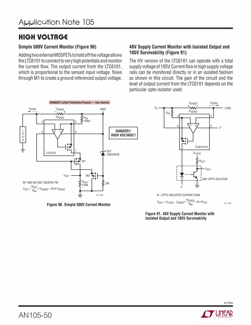
Application Note 105
AN105-50
an105fa
HIGH VOLTAGESimple 500V Current Monitor (Figure 90)
Adding two external MOSFETs to hold off the voltage allows the LTC6101 to connect to very high potentials and monitor the current flow. The output current from the LTC6101, which is proportional to the sensed input voltage, flows through M1 to create a ground referenced output voltage.
48V Supply Current Monitor with Isolated Output and 105V Survivability (Figure 91)
The HV version of the LTC6101 can operate with a total supply voltage of 105V. Current flow in high supply voltage rails can be monitored directly or in an isolated fashion as shown in this circuit. The gain of the circuit and the level of output current from the LTC6101 depends on the particular opto-isolator used.
6101 TA09
LTC6101
RIN100Ω
VOUT
ROUT4.99k
LOAD
–+
VOUT = • VSENSE = 49.9 VSENSEROUTRIN
M1 AND M2 ARE FQD3P50 TM
M1
M2
62VCMZ59448
500V
2M
VSENSE
RSENSE
ISENSE+–
DANGER! Lethal Potentials Present — Use Caution
DANGER!!HIGH VOLTAGE!!
52
1
34
6101 TA08
LTC6101HV
RIN
V–
V–
25
43
VSENSE
RSENSE
ISENSE
LOAD
+–
–+
VOUT = VLOGIC – ISENSE • • N • ROUTRSENSE
RIN
N = OPTO-ISOLATOR CURRENT GAIN
VS
ANY OPTO-ISOLATOR
ROUT
VOUT
VLOGIC
Figure 91. 48V Supply Current Monitor with Isolated Output and 105V Survivability
Figure 90. Simple 500V Current Monitor

Application Note 105
AN105-51
an105fa
Low Power, Bidirectional 60V Precision High Side Current Sense (Figure 92)
Using a very precise zero-drift amplifier as a pre-amp al-lows for the use of a very small sense resistor in a high voltage supply line. A floating power supply regulates the
HIGH VOLTAGE
–
+
LT1787HV
VS– VS
+
4.7µF
VOUT = 2.5V +1000* VSENSE
2.5V REF
1
5 3
53
1
164
4
2
2
8
5
6
72
4
PRECISIONBIDIRECTIONALHIGH VOLTAGELEVEL SHIFT
AND GAIN OF 8
0.1µF
10µF10µF 1µF0.1µF100Ω
LTC2054
BAT54
LTC1754-51N4686
3.9VZ
33Ω
2N5401
MPSA42
– +VSENSE
POSITIVE SENSE
10mΩ
PRECISION BIDIRECTIONAL
GAIN OF 125
12.4k
POWER SUPPLY(NOTE: POSITIVE CURRENT SENSE
INCLUDES CIRCUITSUPPLY CURRENT)
20545 TA06
35.7k
ON 5VOFF 0V
100Ω
voltage across the pre-amplifier on any voltage rail up to the 60V limit of the LT1787HV circuit. Overall gain of this circuit is 1000. A 1mA change in current in either direction through the 10mΩ sense resistor will produce a 10mV change in the output voltage.
Figure 92. Low Power, Bidirectional 60V Precision High Side Current Sense

Application Note 105
AN105-52
an105fa
HIGH VOLTAGEHigh Voltage Current and Temperature Monitoring (Figure 93)
Combining an LTC2990 ADC converter with a high voltage LTC6102HV current sense amplifier allows the measure-ment of very high voltage rails, up to 104V, and very high current loads. The current sense amplifier outputs a ground
–+–INS 0.1µF
VIN5V TO 105V
0.1µF
470pF
ALL CAPACITORS ±20%
VOLTAGE, CURRENT AND TEMPERATURE CONFIGURATION:CONTROL REGISTER: 0x58TAMB REG 4, 5 0.0625°C/LSBVLOAD REG 6, 7 13.2mVLSBV2(ILOAD) REG 8, 9 1.223mA/LSBTREMOTE REG A, B 0.0625°C/LSBVCC REG E, F 2.5V + 305.18µV/LSB
MMBT3904
RIN20Ω1%
ILOAD0A TO 10A
ROUT4.99k1%
200k1%
4.75k1%
0.1µF
RSENSE1mΩ1%
–INFV+V–
LTC6102HVOUT
VREG
+IN
VCC V1
LTC2990
2-WIREI2C
INTERFACE
5V
GND
SDASCLADR0ADR1
V3
V4
V2
2990 TA02
0.1µF
referenced voltage proportional to the load current and is measured as a single ended input by the ADC. A divided down representation of the supply voltage is a second input. An external NPN transistor serves as a remote temperature sensor.
Figure 93. High Voltage Current and Temperature Monitoring

Application Note 105
AN105-53
an105fa
HIGH VOLTAGEMore High Voltage Circuits Are Shown In Other Chapters:
FIGURE TITLE22 Wide Voltage Range Current Sensing23 Smooth Current Monitor Output Signal by Simple Filtering105 High Voltage, 5A High Side Current Sensing in Small Package124 Monitor H-Bridge Motor Current Directly128 Fixed Gain DC Motor Current Monitor167 Monitor Current in an Isolated Supply Line168 Monitoring a Fuse Protected Circuit179 Digitizing Charging and Loading Current in a Battery Monitor182 Power Sensing with Built In A to D Converter183 Isolated Power Measurement184 Fast Data Rate Isolated Power Measurement185 Adding Temperature Measurement to Supply Power Measurement186 Current, Voltage and Fuse Monitoring187 Automotive Socket Power Monitoring188 Power over Ethernet, PoE, Monitoring

Application Note 105
AN105-54
an105fa
Single-Supply 2.5V Bidirectional Operation with External Voltage Reference and I/V Converter (Figure 94)
The LT1787’s output is buffered by an LT1495 rail-to-rail op amp configured as an I/V converter. This configuration is ideal for monitoring very low voltage supplies. The LT1787’s VOUT pin is held equal to the reference voltage appearing at the op amp’s noninverting input. This al-lows one to monitor supply voltages as low as 2.5V. The op amp’s output may swing from ground to its positive supply voltage. The low impedance output of the op amp may drive following circuitry more effectively than the high output impedance of the LT1787. The I/V converter configuration also works well with split supply voltages.
LOW VOLTAGE1.25V Electronic Circuit Breaker (Figure 95)
The LTC4213 provides protection and automatic circuit breaker action by sensing drain-to-source voltage drop across the N-MOSFET. The sense inputs have a rail-to-rail common mode range, so the circuit breaker can protect bus voltages from 0V up to 6V. Logic signals flag a trip condition (with the READY output signal) and reinitialize the breaker (using the ON input). The ON input may also be used as a command in a “smart switch” application.
2.5V
C11µF
RSENSEISENSE
2.5V + VSENSE(MAX)
TOCHARGER/
LOAD
VOUT A
1M5%
1787 F07
LT1495
C31000pF
LT1389-1.25
2.5V +
–A1
1
2
3
4
8
7
6
5
LT1787FIL+FIL–
VBIAS
VOUT
VS– VS
+
DNC
VEE
ROUT
OFF ON
LTC4213
VCC
ON READY
10k
ISELGND
GATE
SI4864DY
VBIAS
VOUT1.25V3.5A
VIN1.25V
VBIAS2.3V TO 6V
SENSENSENSEP
4213 TA01
Figure 94. Single-Supply 2.5V Bidirectional Operation with External Voltage Reference and I/V Converter
Figure 95. 1.25V Electronic Circuit Breaker

Application Note 105
AN105-55
an105fa
Sensing high currents accurately requires excellent control of the sensing resistance, which is typically a very small value to minimize losses, and the dynamic range of the measurement circuitry
Kelvin Input Connection Preserves Accuracy Despite Large Load Currents (Figure 96)
Kelvin connection of the –IN and +IN inputs to the sense resistor should be used in all but the lowest power ap-plications. Solder connections and PC board interconnec-tions that carry high current can cause significant error in measurement due to their relatively large resistances. By isolating the sense traces from the high current paths, this error can be reduced by orders of magnitude. A sense resistor with integrated Kelvin sense terminals will give the best results.
than the max current spec allowed unless the max current is limited in another way, such as with a Schottky diode across RSENSE. This will reduce the high current measure-ment accuracy by limiting the result, while increasing the low current measurement resolution. This approach can be helpful in cases where an occasional large burst of current may be ignored.
HIGH CURRENT (100mA to Amps)
LTC6101ROUT
VOUT
6101 F02
3
5
4
2
1
RIN
V+
LOAD
RSENSE
–+
Figure 96. Kelvin Input Connection Preserves Accuracy Despite Large Load Currents
Figure 97. Shunt Diode Limits Maximum Input Voltage to Allow Better Low Input Resolution Without Over-Ranging the LTC6101
Figure 98. Kelvin Sensing
Shunt Diode Limits Maximum Input Voltage to Allow Better Low Input Resolution Without Over-Ranging the LTC6101 (Figure 97)
If low sense currents must be resolved accurately in a system that has very wide dynamic range, more gain can be taken in the sense amplifier by using a smaller value for resistor RIN. This can result in an operating current greater
V+
LOAD
DSENSE
6101 F03a
RSENSE
Kelvin Sensing (Figure 98)
In any high current, >1A, application, Kelvin contacts to the sense resistor are important to maintain accuracy. This simple illustration from a battery charger application shows two voltage-sensing traces added to the pads of the current sense resistor. If the voltage is sensed with high impedance amplifier inputs, no IxR voltage drop errors are developed.
CSP
4008 F12
DIRECTION OF CHARGING CURRENT
RSENSE
BAT

Application Note 105
AN105-56
an105fa
0A to 33A High Side Current Monitor with Filtering (Figure 99)
High current sensing on a high voltage supply rail is eas-ily accomplished with the LT6100. The sense amplifier is biased from a low 3V supply and pin strapped to a gain of 25V/V to output a 2.5V full-scale reading of the current flow. A capacitor at the FIL pin to ground will filter out noise of the system (220pF produces a 12kHz lowpass corner frequency).
VEE
VOUT
4
FIL
A4VCC
VS+
RSENSE3mΩ
8
VS–
1
3V
CONFIGURED FOR GAIN = 25V/V
4.4V TO 48VSUPPLY
A2
72 6
LT6100
3
5
6100 TA01a
VOUT = 2.5VISENSE = 33A
220pF
LOAD
HIGH CURRENT (100mA to Amps)
Figure 99. 0A to 33A High Side Current Monitor with Filtering
Figure 100. Single Supply RMS Current Measurement
V+
LTC1966IN1
VOUT = 4mVDC/ARMSCAVE1µF
0.1µF
IN2
1966 TA08
VOUTAC CURRENT
75A MAX50Hz TO 400Hz
OUT RTN
GND ENVSS100k
100k
10Ω
T1: CR MAGNETICS CR8348-2500-N www.crmagnetics.com
T1
Single Supply RMS Current Measurement (Figure 100)
The LT1966 is a true RMS-to-DC converter that takes a single-ended or differential input signal with rail-to-rail range. The output of a PCB mounted current sense trans-former can be connected directly to the converter. Up to 75A of AC current is measurable without breaking the signal path from a power source to a load. The accurate operating range of the circuit is determined by the selection of the transformer termination resistor. All of the math is built in to the LTC1966 to provide a DC output voltage that is proportional to the true RMS value of the current. This is valuable in determining the power/energy consumption of AC-powered appliances.

Application Note 105
AN105-57
an105fa
HIGH CURRENT (100mA to Amps)
6101 F03b
–+ –+
–+
R57.5k
VIN
301301
VOUT
ILOAD
5
1
3
LTC6101
2
4
RSENSE LO100m
M1Si4465
10k
CMPZ4697
7.5k
VIN
1.74M4.7k
Q1CMPT5551
40.2k
3
4
5
6
12
8
7
619k
HIGHRANGE
INDICATOR(ILOAD > 1.2A)
VLOGIC(3.3V TO 5V)
LOW CURRENT RANGE OUT2.5V/A
(VLOGIC +5V) ≤ VIN ≤ 60V
0 ≤ ILOAD ≤ 10A
HIGH CURRENT RANGE OUT250mV/A
301 301
5
1
3
LTC6101
2
4
RSENSE HI10m
VLOGIC
BAT54C
LTC1540
Figure 101. Dual LTC6101’s Allow High-Low Current Ranging
Dual LTC6101’s Allow High-Low Current Ranging (Figure 101)
Using two current sense amplifiers with two values of sense resistors is an easy method of sensing current over a wide range. In this circuit the sensitivity and resolution of
measurement is 10 times greater with low currents, less than 1.2A, than with higher currents. A comparator detects higher current flow, up to 10A, and switches sensing over to the high current circuitry.

Application Note 105
AN105-58
an105fa
LDO Load Balancing (Figure 102)
As system design enhancements are made there is often the need to supply more current to a load than originally expected. A simple way to modify power amplifiers or voltage regulators, as shown here, is to parallel devices. When paralleling devices it is desired that each device shares the total load current equally. In this circuit two adjustable “slave” regulator output voltages are sensed
HIGH CURRENT (100mA to Amps)and servo’ed to match the master regulator output volt-age. The precise low offset voltage of the LTC6078 dual op amp (10µV) balances the load current provided by each regulator to within 1mA. This is achieved using a very small 10mΩ current sense resistor in series with each output. This sense resistor can be implemented with PCB copper traces or thin gauge wire.
VDD
60789 TA09
1k
VIN1.8V TO 20V
10µF0.01µF
0.1µF
10µF
LOADILOAD
IN OUT
SHDN
LT1763
BYP
FB
+
–A
R12k
R22k
0 ≤ ILOAD ≤ 1.5A1.22V ≤ VOUT ≤ VDDLDO LOADS MATCH TO WITHIN 1mA WITH 10mΩ OF BALLASTRESISTANCE (2 INCHES OF AWG 28 GAUGE STRANDED WIRE)A, B: LTC6078
BALLAST RESISTANCE:IDENTICAL LENGTHTHERMALLY MATEDWIRE OR PCB TRACE
+
10µF0.01µF
IN OUT
SHDN
LT1763
BYP
FB2k
10k
2k
100Ω
1k0.1µF
10µF0.01µF
IN OUT
SHDN
LT1763
BYP
FB2k
10k
2k
100Ω
+
–B
R2R1VOUT = 1.22V 1 +( )
Figure 102. LDO Load Balancing

Application Note 105
AN105-59
an105fa
HIGH CURRENT (100mA to Amps)
Figure 103. Sensing Output Current
Sensing Output Current (Figure 103)
The LT1970 is a 500mA power amplifier with voltage programmable output current limit. Separate DC voltage inputs and an output current sensing resistor control the maximum sourcing and sinking current values. These control voltages could be provided by a D-to-A converter
in a microprocessor controlled system. For closed loop control of the current to a load an LT1787 can monitor the output current. The LT1880 op amp provides scaling and level shifting of the voltage applied to an A-to-D converter for a 5mV/mA feedback signal.
VCSRC
COMMONVEE
VCSNK
V–FILTER
V+
12V
ENVCC
ISNKISRC
SENSE–SENSE+
TSDOUT
+IN
VCC0V TO 1V
LT1970
–12V
–IN
RS0.2Ω
RLOAD
1970 F10
RG RFVS
–
VEE
20k
BIAS–12V
–12V
R160.4k
R4255k
VOUT2.5V±5mV/mA
1kHz FULL CURRENTBANDWIDTH
R210k
R320k
VS+
LT1787
–
+LT1880
12V
–12V
0V TO 5V A/D
OPTIONAL DIGITAL FEEDBACK

Application Note 105
AN105-60
an105fa
HIGH CURRENT (100mA to Amps)Using Printed Circuit Sense Resistance (Figure 104)
The outstanding LTC6102 precision allows the use of sense resistances fabricated with conventional printed circuit techniques. For “one ounce” copperclad, the trace resistance is approximately (L/W)·0.0005Ω and can carry about 4A per mm of trace width. The example below shows a practical 5A monitoring solution with both L and W set to 2.5mm. The resistance is subject to about +0.4%/ºC temperature change and the geometric tolerances of the fabrication process, so this will not generally be for high accuracy work, but can be useful in various low cost protection and status monitoring functions.
High Voltage, 5A High Side Current Sensing in Small Package (Figure 105)
The LT6106 is packaged in a small SOT-23 package but still operates over a wide supply range of 3V to 44V. Just two resistors set the gain (10 in circuit shown) and the output is a voltage referred to ground.
DN423 F02
TO LOAD10A MAX
FROMSUPPLY
V–OUTPUT
ROUTLTC6102
RIN– RIN
+
CREG
* 2.5mm × 2.5mm1oz COPPER500µΩ
V–
RSENSE*
CURRENT CARRYING TRACEL
W
LT61061k
VOUT200mV/A
6106 TA01a
100Ω
3V TO 36V
LOAD
0.02Ω
–+
V+V–
OUT
–IN+IN
Figure 104. Using Printed Circuit Sense Resistance
Figure 105. High Voltage, 5A High Side Current Sensing in Small Package
More High Current Circuits Are Shown in Other Chapters:FIGURE TITLE
59 Differential Output Bidirectional 10A Current Sense93 High Voltage Current and Temperature Monitoring121 Single Output Provides 10A H-Bridge Current and Direction179 Digitizing Charging and Loading Current in a Battery Monitor209 Use Kelvin Connections to Maintain High Current Accuracy215 0 to 10A Sensing Over Two Ranges

Application Note 105
AN105-61
an105fa
For low current applications the easiest way to sense cur-rent is to use a large sense resistor. This however causes larger voltage drops in the line being sensed which may not be acceptable. Using a smaller sense resistor and taking gain in the sense amplifier stage is often a better approach. Low current implies high source impedance measurements which are subject approach. Low current implies high source impedance measurements which are subject to noise pickup and often require filtering of some sort.
Filtered Gain of 20 Current Sense (Figure 106)
The LT6100 has pin strap connections to establish a variety of accurate gain settings without using external compo-nents. For this circuit grounding A2 and leaving A4 open set a gain of 20. Adding one external capacitor to the FIL pin creates a lowpass filter in the signal path. A capacitor of 1000pF as shown sets a filter corner frequency of 2.6KHz.
0nA to 200nA Current Meter (Figure 108)
A floating amplifier circuit converts a full-scale 200nA flowing in the direction indicated at the inputs to 2V at the output of the LT1495. This voltage is converted to a current to drive a 200µA meter movement. By floating the power to the circuit with batteries, any voltage potential at the inputs are handled. The LT1495 is a micropower op amp so the quiescent current drain from the batteries is very low and thus no on/off switch is required.
LOW CURRENT (Picoamps to Milliamps)
VOUT20 • RSENSE • ISENSE
–3dB AT 2.6kHz
FIL
VCC
6100 TA03
RSENSE
LT6100 VS–VS
+
VEE A2 A4
3V
1000pF
VSUPPLY4.4V TO 48V
ISENSE
LOAD
–+
Figure 106. Filtered Gain of 20 Current Sense
Figure 108. 0nA to 200nA Current Meter
Figure 107. Gain of 50 Current Sense
Gain of 50 Current Sense (Figure 107)
The LT6100 is configured for a gain of 50 by grounding both A2 and A4. This is one of the simplest current sensing amplifier circuits where only a sense resistor is required.
VOUT50 • RSENSE • ISENSE
FIL
VCC
6100 TA04
RSENSE
LT6100 VS–VS
+
VEE A2 A4
5V
VSUPPLY6.4V TO 48V
ISENSE
–+
LOAD
–
+
–
+
µA
1495 TA06
1/2LT1495
1/2LT1495
100pF
R110M
R29k
1.5V
1.5V
R32kFULL-SCALEADJUST
IS = 3µA WHEN IIN = 0NO ON/OFF SWITCH REQUIRED
0µA TO200µA
R410k
INPUTCURRENT

Application Note 105
AN105-62
an105fa
Lock-In Amplifier Technique Permits 1% Accurate APD Current Measurement Over 100nA to 1mA Range (Figure 109)
Avalanche Photodiodes, APDs, require a small amount of current from a high voltage supply. The current into the diode is an indication of optical signal strength and must be monitored very accurately. It is desirable to power all of the support circuitry from a single 5V supply.
This circuit utilizes AC carrier modulation techniques to meet APD current monitor requirements. It features 0.4% accuracy over the sensed current range, runs from a 5V supply and has the high noise rejection characteristics of carrier based “lock in” measurements.
The LTC1043 switch array is clocked by its internal oscillator. Oscillator frequency, set by the capacitor at Pin 16, is about 150Hz. S1 clocking biases Q1 via level shifter Q2. Q1 chops the DC voltage across the 1k current
LOW CURRENT (Picoamps to Milliamps)
shunt, modulating it into a differential square wave signal which feeds A1 through 0.2µF AC coupling capacitors. A1’s single-ended output biases demodulator S2, which presents a DC output to buffer amplifier A2. A2’s output is the circuit output.
Switch S3 clocks a negative output charge pump which supplies the amplifier’s V– pins, permitting output swing to (and below) zero volts. The 100k resistors at Q1 minimize its on-resistance error contribution and prevent destruc-tive potentials from reaching A1 (and the 5V rail) if either 0.2µF capacitor fails. A2’s gain of 1.1 corrects for the slight attenuation introduced by A1’s input resistors. In practice, it may be desirable to derive the APD bias voltage regula-tor’s feedback signal from the indicated point, eliminating the 1kΩ shunt resistor’s voltage drop. Verifying accuracy involves loading the APD bias line with 100nA to 1mA and noting output agreement.
OUTPUT0V TO 1V = 0mA TO 1mA
5V
+
–
5V
A1LT1789
–3.5V0.2µF
S1
0.2µF
VOUT = 20V TO 90VTO APD
FOR OPTIONAL “ZERO CURRENT” FEEDBACK TOAPD BIAS REGULATOR, SEE APPENDIX A
APDHIGH VOLTAGE
BIAS INPUT
AN92 F04
1k*1%
100k*
–
+
5V
A2LT1006
–3.5V
100k*Q1
1M*
1M*Q2MPSA42
5VS3
S2
20k
15
16 17 4
318
5
26
12
13 14
22µF
22µF
–3.5V TOAMPLIFIERS
0.056µF
5V
20k*
20k
200k*
1µF
1µF
1µF100V
1µF100V
30k10k
1N46905.6V
#
= 1N4148
= 0.1% METAL FILM RESISTOR= TECATE CMC100105MX1825= LTC1043 PIN NUMBER
= TP0610L
*1µF 100V
CIRCLED NUMBERS
+
+
Figure 109. Lock-In Amplifier Technique Permits 1% Accurate APD Current Measurement Over 100nA to 1mA Range

Application Note 105
AN105-63
an105fa
DC-Coupled APD Current Monitor (Figure 110)
Avalanche Photodiodes, APDs, require a small amount of current from a high voltage supply. The current into the diode is an indication of optical signal strength and must be monitored very accurately. It is desirable to power all of the support circuitry from a single 5V supply.
This circuit’s DC-coupled current monitor eliminates the previous circuit’s trim but pulls more current from the APD bias supply. A1 floats, powered by the APD bias rail. The 15V Zener diode and current source Q2 ensure A1 never is exposed to destructive voltages. The 1kΩ current shunt’s voltage drop sets A1’s positive input potential. A1 balances its inputs by feedback controlling its negative input via Q1. As such, Q1’s source voltage equals A1’s positive input voltage and its drain current sets the voltage across its source resistor. Q1’s drain current produces a voltage
LOW CURRENT (Picoamps to Milliamps)
Figure 110. DC-Coupled APD Current Monitor
drop across the ground referred 1kΩ resistor identical to the drop across the 1kΩ current shunt and, hence, APD current. This relationship holds across the 20V to 90V APD bias voltage range. The 5.6V zener assures A1’s inputs are always within their common mode operating range and the 10MΩ resistor maintains adequate Zener current when APD current is at very low levels.
Two output options are shown. A2, a chopper stabilized amplifier, provides an analog output. Its output is able to swing to (and below) zero because its V– pin is supplied with a negative voltage. This potential is generated by us-ing A2’s internal clock to activate a charge pump which, in turn, biases A2’s V– Pin 3. A second output option substitutes an A-to-D converter, providing a serial format digital output. No V– supply is required, as the LTC2400 A-to-D will convert inputs to (and slightly below) zero volts.
Hi-Z OUTPUT0V TO 1V = 0mA TO 1mA
–
+A1
LT1077
VOUT = 20V TO 90VTO APD
APDHIGH VOLTAGE
BIAS INPUT
AN92 F05
1k*CURRENT SHUNT
1k*
–
+A2
LTC1150CLK OUT
BUFFERED OUTPUT0mA TO 1mA = 0V TO 1V5V
V –
≈ –3.5V HERE
51k
10k
1k*
1k*
51K
Q2MPSA42
Q22N3904
10µF
10µF
Q1ZVP0545A
100k
39k
1k
5V
1µF
= BAT85
= 0.1% METAL FILM RESISTOR*
10M
1N46905.6V
1N470215V
5V
5V
100k
VIN VREF
LTC2400A-TO-D
OPTIONALDIGITAL OUTPUT
OPTIONAL BUFFERED OUTPUT
FO
SCKDIGITALINTERFACESDO
CS
LT14602.5V
+
+
+
FOR OPTIONAL “ZERO CURRENT” FEEDBACK TOAPD BIAS REGULATOR, SEE APPENDIX A

Application Note 105
AN105-64
an105fa
LOW CURRENT (Picoamps to Milliamps)Six Decade (10nA to 10mA) Current Log Amplifier (Figure 111)
Using precision quad amplifiers like the LTC6079, (10µV offset and <1pA bias current) allow for very wide range
current sensing. In this circuit a six decade range of current pulled from the circuit input terminal is converted to an output voltage in logarithmic fashion increasing 150mV for every decade of current change.
60789 TA07
VDD
VCC
133k100k
Q1
1000pF
VOUT
1µF 10nA ≤ IIN ≤ 10mAQ1, Q2: DIODES INC. DMMT3906WA TO D: LTC6079VOUT ≈ 150mV • log (IIN) + 1.23V, IIN IN AMPS
PRECISION RESISTOR PT1461k+3500ppm/°C
100Ω
1.58k
+
–D
+
–B
+
–C
+
–A
1µF
Q2
33µF
IIN
100Ω
GND
LT6650
IN OUT
Figure 111. Six Decade (10nA to 10mA) Current Log Amplifier

Application Note 105
AN105-65
an105fa
The largest challenge in measuring current through induc-tive circuits is the transients of voltage that often occur. Current flow can remain continuous in one direction while the voltage across the sense terminals reverses in polarity.
Electronic Circuit Breaker (Figure 112)
The LTC1153 is an electronic circuit breaker. Sensed cur-rent to a load opens the breaker when 100mV is developed between the supply input, VS, and the drain sense pin, DS. To avoid transient, or nuisance trips of the break compo-nents RD and CD delay the action for 1ms. A thermistor can also be used to bias the shutdown input to monitor heat generated in the load and remove power should the temperature exceed 70°C in this example. A feature of the LTC1153 is timed automatic reset which will try to reconnect the load after 200ms using the 0.22μF timer capacitor shown.
A common monitoring approach in these systems is to amplify the voltage on a “flying” sense resistor, as shown. Unfortunately, several potentially hazardous fault scenarios go undetected, such as a simple short to ground at a motor terminal. Another complication is the noise introduced by the PWM activity. While the PWM noise may be filtered for purposes of the servo law, information useful for protection becomes obscured. The best solution is to simply provide two circuits that individually protect each half-bridge and report the bidirectional load current. In some cases, a smart MOSFET bridge driver may already include sense resistors and offer the protection features needed. In these situations, the best solution is the one that derives the load information with the least additional circuitry.
IN
CT
STATUS
GND
VS
DS
G
SHUTDOWN
LTC1153
CD0.01µF
RD100k
*RSEN 0.1Ω
IRLR024
51k
SENSITIVE5V LOAD
**70°CPTC
51k
5V
TO µP
CT0.22µF
ON/OFF
ALL COMPONENTS SHOWN ARE SURFACE MOUNT.IMS026 INTERNATIONAL MANUFACTURING SERVICE, INC. (401) 683-9700RL2006-100-70-30-PT1 KEYSTONE CARBON COMPANY (814) 781-1591
***
LTC1153 • TA01
Z5U
Conventional H-Bridge Current Monitor (Figure 113)
Many of the newer electric drive functions, such as steer-ing assist, are bidirectional in nature. These functions are generally driven by H-bridge MOSFET arrays using pulse-width modulation (PWM) methods to vary the commanded torque. In these systems, there are two main purposes for current monitoring. One is to monitor the current in the load, to track its performance against the desired com-mand (i.e., closed-loop servo law), and another is for fault detection and protection features.
–
+
+
IM
RS
BATTERY BUS
DIFFAMP
DN374 F03
Motor Speed Control (Figure 114)
This uses an LT1970 power amplifier as a linear driver of a DC motor with speed control. The ability to source and sink the same amount of output current provides for bidirectional rotation of the motor. Speed control is managed by sensing the output of a tachometer built on to the motor. A typical feedback signal of 3V/1000rpm is compared with the desired speed-set input voltage. Be-cause the LT1970 is unity-gain stable, it can be configured as an integrator to force whatever voltage across the mo-tor as necessary to match the feedback speed signal with the set input signal. Additionally, the current limit of the amplifier can be adjusted to control the torque and stall current of the motor.
MOTORS AND INDUCTIVE LOADS
Figure 112. Electronic Circuit Breaker
Figure 113. Conventional H-Bridge Current Monitor

Application Note 105
AN105-66
an105fa
Practical H-Bridge Current Monitor Offers Fault Detection and Bidirectional Load Information (Figure 115)
This circuit implements a differential load measurement for an ADC using twin unidirectional sense measurements. Each LTC6101 performs high side sensing that rapidly responds to fault conditions, including load shorts and MOSFET failures. Hardware local to the switch module (not shown in the diagram) can provide the protection logic and furnish a status flag to the control system. The two LTC6101 outputs taken differentially produce a bidirectional load measurement for the control servo. The ground-referenced signals are compatible with most ΔΣADCs. The ΔΣADC circuit also provides a “free” in-tegration function that removes PWM content from the measurement. This scheme also eliminates the need for analog-to-digital conversions at the rate needed to sup-port switch protection, thus reducing cost and complexity.
VCSRC
COMMON
R449.9k
15V
–15V
REVERSE
FORWARD
R210k
VEE
VCSNK
V–FILTER
V+
15V
ENVCC
ISNKISRC
SENSE–SENSE+
TSDOUT
+IN
LT1970
–15V
–IN
RS1Ω
12V DCMOTOR
TACHFEEDBACK3V/1000rpm
GND
1970 F13
C11µF
R549.9k
R31.2k
R11.2k
OV TO 5VTORQUE/STALL
CURRENT CONTROL
+
IM
BATTERY BUS
DN374 F04
LTC6101
RS RS
RIN RINROUT
LTC6101ROUT
DIFFOUTPUTTO ADC
FOR IM RANGE = ±100A,DIFF OUT = ±2.5V
RS = 1mΩRIN = 200ΩROUT = 4.99k
+
–
MOTORS AND INDUCTIVE LOADS
Figure 114. Motor Speed Control
Figure 115. Practical H-Bridge Current Monitor Offers Fault Detection and Bidirectional Load Information

Application Note 105
AN105-67
an105fa
Lamp Driver (Figure 116)
The inrush current created by a lamp during turn-on can be 10 to 20 times greater than the rated operating cur-rent. This circuit shifts the trip threshold of an LTC1153 electronic circuit breaker up by a factor of 11:1 (to 30A) for 100ms while the bulb is turned on. The trip threshold then drops down to 2.7A after the inrush current has subsided.
IN
CT
STATUS
GND
VS
DS
G
SD
LTC11530.33µF
+470µF
IRFZ34
12V
12V
0.02Ω
LTC1153 • TA07
10k
1M0.1µF
VN2222LL
100k
12V/2ABULB
5V
Intelligent High Side Switch (Figure 117)
The LT1910 is a dedicated high side MOSFET driver with built in protection features. It provides the gate drive for a power switch from standard logic voltage levels. It provides shorted load protection by monitoring the current flow to through the switch. Adding an LTC6101 to the same circuit, sharing the same current sense resistor, provides a linear voltage signal proportional to the load current for additional intelligent control.
6101 TA07
LOAD
FAULT
OFF ON
1 54.99k
VORS
3
4
47k
2
8
6
100Ω
100Ω1%
10µF63V
1µF
14VVLOGIC
SUB85N06-5
VO = 49.9 • RS • IL
FOR RS = 5mΩ,VO = 2.5V AT IL = 10A (FULL-SCALE)
LT1910 LTC6101
IL
5
2
1
3
4
MOTORS AND INDUCTIVE LOADS
Figure 116. Lamp Driver
Figure 117. Intelligent High Side Switch

Application Note 105
AN105-68
an105fa
Relay Driver (Figure 118)
This circuit provides reliable control of a relay by using an electronic circuit breaker circuit with two-level over-current protection. Current flow is sensed through two separate resistors, one for the current into the relay coil and the other for the current through the relay contacts. When 100mV is developed between the VS supply pin and the drain sense pin, DS, the N-channel MOSFET is turned off opening the contacts. As shown, the relay coil current is limited to 350mA and the contact current to 5A.
Full-Bridge Load Current Monitor (Figure 119)
The LT1990 is a difference amplifier that features a very wide common mode input voltage range that can far exceed its own supply voltage. This is an advantage to reject transient voltages when used to monitor the current in a full-bridge driven inductive load such as a motor. The LT6650 provides a voltage reference of 1.5V to bias up the output away from ground. The output will move above or below 1.5V as a function of which direction the current in the load is flowing. As shown, the amplifier provides a gain of 10 to the voltage developed across resistor RS.
IN
CT
STATUS
GND
VS
DS
G
SD
LTC11531µF MTD3055E
15V
12V
LTC1153 • TA08
5V0.01µF
+100µF
10k
1N4148
1N4001
2Ω 0.02Ω
TO 12VLOAD
COIL CURRENT LIMITED TO 350mACONTACT CURRENT LIMITED TO 5A
RS
+VSOURCE
IL
–12V ≤ VCM ≤ 73VVOUT = VREF ± (10 • IL • RS)
–
+
40k40k 100k
100k
900k
1M
1M
900k 10k
10k
VOUT
LT1990
LT6650 GND
IN OUT
FB
54.9k
20k
1nF
1µF
VREF = 1.5V
1990 TA01
5V
7
2
3
4
1
8
6
5
+–
MOTORS AND INDUCTIVE LOADS
Figure 118. Relay Driver
Figure 119. Full-Bridge Load Current Monitor

Application Note 105
AN105-69
an105fa
Bidirectional Current Sensing in H-Bridge Drivers (Figure 120)
Each channel of an LTC6103 provides measurement of the supply current into a half-bridge driver section. Since only one of the half-bridge sections will be conducting current in the measurable direction at any given time, only one output at a time will have a signal. Taken differentially, the
V+
4V TO 60V
4.99kDIFFERENTIALOUTPUT±2.5V FS (MAY BE LIMITED IF V+ < 6V)±10A FS
+
+–
–4.99k
6103 TA04
PWM*
*USE “SIGN-MAGNITUDE” PWM FOR ACCURATE LOAD CURRENT CONTROL AND MEASUREMENT
PWM*
+ – +–
8 7 6 5
241
+INA
OUTA OUTB
VSBVSA
LTC6103
–INA –INB
200Ω
10mΩ 10mΩ
200Ω
+INB
V–
two outputs form a bidirectional measurement for subse-quent circuitry, such as an ADC. In this configuration, any load fault to ground will also be detected so that bridge protection can be implemented. This arrangement avoids the high frequency common mode rejection problem that can cause problems in “flying” sense resistor circuits.
Figure 120. Bidirectional Current Sensing in H-Bridge Drivers
MOTORS AND INDUCTIVE LOADS

Application Note 105
AN105-70
an105fa
Single Output Provides 10A H-Bridge Current and Direction (Figure 121)
The output voltage of the LTC6104 will be above or below the external 2.5V reference potential depending on which side of the H-bridge is conducting current. Monitoring the current in the bridge supply lines eliminates fast voltage changes at the inputs to the sense amplifiers.
6104 TA02
VBATTERY(8V TO 60V)
3V TO 18V
78 5
6
4
PWM*
249Ω
2
4.99k
1µF
VO
10m10m
LT1790-2.5
4
6
21
PWM*
VO = 2.5V ±2V (±10A FS)
*USE “SIGN-MAGNITUDE” PWM FOR ACCURATELOAD CURRENT CONTROL AND MEASUREMENT
249Ω
0.1µF
IM
LTC6104
Figure 121. Single Output Provides 10A H-Bridge Current and Direction
Figure 122. Monitor Solenoid Current on the Low Side
Figure 123. Monitor Solenoid Current on the High Side
6105 F06
LT6105
V–
V+
2k1%
2k1%
24V, 3WSOLENOID
200Ω1%
1N5818
TP0610L
1N914
–IN +IN
4.99k1%
200Ω1%
VOUT = 25mV/mAVOUT
5VDC
24VDC
19V/ON24V/OFF
– +
1Ω1%
Monitor Solenoid Current on the Low Side (Figure 122)
Driving an inductive load such as a solenoid creates large transients of common mode voltage at the inputs to a current sense amplifier. When de-energized the voltage across the solenoid reverses (also called the freewheel state) and tries to go above its power supply voltage but is clamped by the freewheel diode. The LT6105 senses the solenoid current continuously over an input voltage range of 0V to one diode drop above the 24V supply.
Monitor Solenoid Current on the High Side (Figure 123)
Driving an inductive load such as a solenoid creates large transients of common mode voltage at the inputs to a current sense amplifier. When de-energized the voltage
6105 F04
LT6105
V–
V+
24V, 3WSOLENOID
200Ω1%
1N5818
2N7000
–IN +IN
4.99k1%
200Ω1%
VOUT = 25mV/mAVOUT
5VDC
24VDC
0V/OFF5V/ON
– +
1Ω1%
across the solenoid reverses (also called the freewheel state) and tries to go below ground but is clamped by the freewheel diode. The LT6105 senses the solenoid current continuously with pull-up resistors keeping the inputs within the most accurate input voltage range.
MOTORS AND INDUCTIVE LOADS
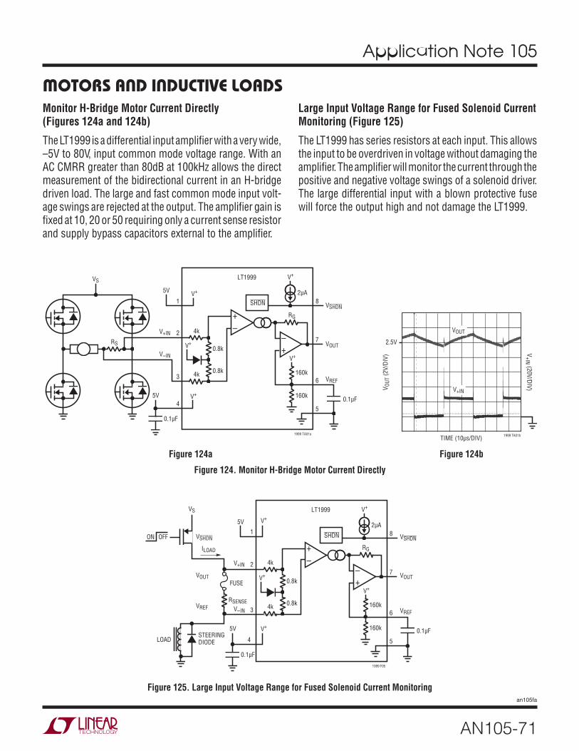
Application Note 105
AN105-71
an105fa
Figure 124a
Figure 125. Large Input Voltage Range for Fused Solenoid Current Monitoring
Figure 124b
Monitor H-Bridge Motor Current Directly (Figures 124a and 124b)
The LT1999 is a differential input amplifier with a very wide, –5V to 80V, input common mode voltage range. With an AC CMRR greater than 80dB at 100kHz allows the direct measurement of the bidirectional current in an H-bridge driven load. The large and fast common mode input volt-age swings are rejected at the output. The amplifier gain is fixed at 10, 20 or 50 requiring only a current sense resistor and supply bypass capacitors external to the amplifier.
LT1999
4k
0.8k
160k
160k
2µA
0.8k4k
SHDN
5V
V+
V+
V+5V
RS
1999 TA01a
+–
+–
VS
81
2
3
4
7
6
50.1µF
0.1µF
VOUT
RG
V+IN
V–IN
VREF
VSHDN
V+
V+
TIME (10µs/DIV)
2.5V
V OUT
(2V/
DIV)
V+IN (20V/DIV)
1999 TA01b
VOUT
V+IN
VOUT
VREF
VSHDN
LT1999
4k
0.8k
160k
160k
2µA
0.8k4k
SHDN
V+
V+
V+
+–
+–
81
2
3
4
7
6
5
RG
V+
V+VS
5V
1999 F05
0.1µF
0.1µF
FUSE
STEERINGDIODELOAD
ILOAD
RSENSE
OFFON
5V
VOUT
V+IN
V–IN VREF
VSHDN
Large Input Voltage Range for Fused Solenoid Current Monitoring (Figure 125)
The LT1999 has series resistors at each input. This allows the input to be overdriven in voltage without damaging the amplifier. The amplifier will monitor the current through the positive and negative voltage swings of a solenoid driver. The large differential input with a blown protective fuse will force the output high and not damage the LT1999.
Figure 124. Monitor H-Bridge Motor Current Directly
MOTORS AND INDUCTIVE LOADS

Application Note 105
AN105-72
an105fa
Monitor Both the ON Current and the Freewheeling Current Through a High Side Driven Solenoid (Figure 126)
Placing the current sense resistor inside the loop created by a grounded solenoid and the freewheeling clamp diode allows for continuous monitoring of the solenoid current while being energized or switched OFF. The LT1999 oper-ates accurately with an input common mode voltage down to –5V below ground.
Monitor Both the ON Current and the Freewheeling Current In a Low Side Driven Solenoid (Figure 127)
Placing the current sense resistor inside the loop created by a grounded solenoid and the freewheeling clamp diode allows for continuous monitoring of the solenoid current while being energized or switched OFF. The LT1999 oper-ates accurately with an input common mode voltage up to 80V. In this circuit the input is clamped at one diode above the solenoid supply voltage.
LT1999
4k
0.8k
160k
160k
2µA
0.8k4k
SHDN
V+
V+
V+
+–
+–
81
2
3
4
7
6
5
RG
V+
V+
5V
VS
5V
1999 F07a
0.1µF
0.1µF
SOLENOID
RSENSE
V+IN
VSHDN
VOUT
VREFV–IN
ONOFF
LT1999
4k
0.8k
160k
160k
2µA
0.8k4k
SHDN
V+
+–
+–
8
2
3
7
6
5
RG
V+
V+
5V
VS
5V
1999 F08a
1
40.1µF
0.1µF
SOLENOID
RSENSE
VOUT
VREF
VSHDN
ON
OFFV+
V+
V+IN
V–IN
Figure 126. Monitor Both the ON Current and the Freewheeling Current Through a High Side Driven Solenoid
Figure 127. Monitor Both the ON Current and the Freewheeling Current In a Low Side Driven Solenoid
MOTORS AND INDUCTIVE LOADS

Application Note 105
AN105-73
an105fa
Figure 128. Fixed Gain DC Motor Current Monitor
Fixed Gain DC Motor Current Monitor (Figure 128)
With no critical external components the LT1999 can be connected directly across a sense resistor in series with an H-bridge driven motor. The amplifier output voltage is
1999 F09
VBRIDGE
V+IN
V–IN
RSENSE0.025Ω
10µF
PWM INPUT
DIRECTION
BRAKE INPUT
24V
5V
5V
GND
5V
PWM INOUTA
OUTB
C41000µF
24V MOTOR
H-BRIDGE
LT1999-20
4k
0.8k
160k
160k
2µA
0.8k4k
SHDN
+–
+–
80k
V+
V+V+
V+0.1µF
0.1µF
8
7
6
VSHDN
VOUT
VREF
2
3
1
4
V+
5
referenced to one-half supply so the direction of motor rotation is indicated by the output being above or below the DC output voltage when stopped.
MOTORS AND INDUCTIVE LOADS

Application Note 105
AN105-74
an105fa
Simple DC Motor Torque Control (Figure 129)
The torque of a spinning motor is directly proportional to the current through it. In this circuit the motor current is monitored and compared to a DC set point voltage. The motor current is sensed by an LT6108-1 and forced to
SENSEHI SENSELO
OUTA
8 1
6
5
7
2
3
4
LT6108-1
V–
9k 100k
2
37 LTC6246
46 1
3
6 IRF640
5V
1N5818
0.1Ω
VMOTOR
5
4
2
0.47µFVOUT
CURRENT SET POINT (0V TO 5V)
1k
1M
610812 TA04
1k
78.7k100k
280k
INC
V+
EN/RST
OUTC
RESET
100µF
+–
LTC6992-1
V+
GND
5V
1µF
BRUSHEDDC MOTOR(0A TO 5A)MABUCHIRS-540SH
MOD
SET
OUT
DIV
match the set point current value through an amplifier and a PWM motor drive circuit. The LTC6992-1 produces a PWM signal from 0% to 100% duty cycle for a 0V to 1V change at the MOD input pin.
Figure 129. Simple DC Motor Torque Control
MOTORS AND INDUCTIVE LOADS

Application Note 105
AN105-75
an105fa
VCC V1
LTC2990
LOADPWR = I • V0.1Ω1%MOTOR CONTROL VOLTAGE
0VDC TO 5VDC0A TO ±2.2A
2-WIREI2C
INTERFACE
5V
GND
470pF
TMOTOR
MMBT3904SDASCLADR0ADR1
V3
V4
V2
2990 TA04
MOTOR
TINTERNAL
CURRENT AND TEMPERATURE CONFIGURATION:CONTROL REGISTER: 0x59TAMB REG 4, 5 0.0625°C/LSBIMOTOR REG 6, 7 194µA/LSBTMOTOR REG A, B 0.0625°C/LSBVCC REG E, F 2.5V + 305.18µV/LSB
VOLTAGE AND TEMPERATURE CONFIGURATION:CONTROL REGISTER: 0x58TAMB REG 4, 5 0.0625°C/LSBVMOTOR REG 8, 9 305.18µVLSBTMOTOR REG A, B 0.0625°C/LSBVCC REG E, F 2.5V + 305.18µV/LSB
0.1µF
VCC V1
LTC2990
LOADPWR = I • V0.01Ω1W, 1%MOTOR CONTROL VOLTAGE
0V TO 40V0A TO 10A
2-WIREI2C
INTERFACE
5V
71.5k1%
71.5k1%
10.2k1%
10.2k1%
GND
470pF
TMOTOR
MMBT3904SDASCLADR0ADR1
V3
V4
V2
2990 TA05
MOTOR
TINTERNAL
VOLTAGE AND TEMPERATURE CONFIGURATION:CONTROL REGISTER: 0x58TAMB REG 4, 5 0.0625°C/LSBVMOTOR REG 8, 9 2.44mVLSBTMOTOR REG A, B 0.0625°C/LSBVCC REG E, F 2.5V + 305.18µV/LSB
CURRENT AND TEMPERATURE CONFIGURATION:CONTROL REGISTER: 0x59TAMB REG 4, 5 0.0625°C/LSBIMOTOR REG 6, 7 15.54mA/LSBTMOTOR REG A, B 0.0625°C/LSBVCC REG E, F 2.5V + 305.18µV/LSB
0.1µF
Small Motor Protection and Control (Figure 130)
DC motor operating current and temperature can be digi-tized and sent to a controller which can then adjust the applied control voltage. Stalled rotor or excessive loading on the motor can be sensed.
Large Motor Protection and Control (Figure 131)
For high voltage/current motors, simple resistor divid-ers can scale the signals applied to an LTC2990 14-bit converter. Proportional DC motor operating current and temperature can be digitized and sent to a controller which can then adjust the applied control voltage. Stalled rotor or excessive loading on the motor can be sensed.
Figure 130. Small Motor Protection and Control
Figure 131. Large Motor Protection and Control
MOTORS AND INDUCTIVE LOADS

Application Note 105
AN105-76
an105fa
The science of battery chemistries and the charging and discharging characteristics is a book of its own. This chap-ter is intended to provide a few examples of monitoring current flow into and out of batteries of any chemistry.
Input Remains Hi-Z when LT6100 is Powered Down (Figure 132)
This is the typical configuration for an LT6100, monitoring the load current of a battery. The circuit is powered from a low voltage supply rail rather than the battery being monitored. A unique benefit of this configuration is that when the LT6100 is powered down, its battery sense inputs remain high impedance, drawing less than 1µA of current. This is due to an implementation of Linear Technology’s Over-The-Top input technique at its front end.
Charge/Discharge Current Monitor on Single Supply with Shifted VBIAS (Figure 133)
Here the LT1787 is used in a single-supply mode with the VBIAS pin shifted positive using an external LT1634 voltage reference. The VOUT output signal can swing above and below VBIAS to allow monitoring of positive or negative currents through the sense resistor. The choice of refer-ence voltage is not critical except for the precaution that adequate headroom must be provided for VOUT to swing without saturating the internal circuitry. The component values shown allow operation with VS supplies as low as 3.1V.
VOUT
FIL
VCC
POWERDOWN OK
INPUTSREMAIN
Hi-Z
VCC
0V3V
6100 F08
RSENSE
LT6100 VS– VS
+
VEE A2 A4
TO LOAD
ISENSE
– +
BATTERY4.1V TO 48V
+
Figure 132. Input Remains Hi-Z when LT6100 is Powered Down
Figure 133. Charge/Discharge Current Monitor on Single Supply with Shifted VBIAS
Figure 134. Battery Current Monitor
C21µF
20k5%
1787 F04
3.3V
LT1634-1.25
*OPTIONAL OUTPUT
C11µF
RSENSE3.3VTO60V
TOCHARGER/
LOAD
1
2
3
4
8
7
6
5
LT1787HVFIL+FIL–
VBIAS
VOUT
VS– VS
+
DNC
VEE
C3*1000pF
ROUT
–
+
–
+
1495 TA05
RSENSE0.1Ω
ILCHARGE
RA
2N3904
VO = IL RSENSE
FOR RA = 1k, RB = 10k
= 1V/A
CHARGEOUT
DISCHARGEOUT
DISCHARGE
2N3904
RA
RA RA
RB
RBRA
VOIL
RB
A11/2 LT1495
5V 12V
A21/2 LT1495
( )
Battery Current Monitor (Figure 134)
One LT1495 dual op amp package can be used to establish separate charge and discharge current monitoring outputs. The LT1495 features Over-the-Top operation allowing the battery potential to be as high as 36V with only a 5V amplifier supply voltage.
BATTERIES

Application Note 105
AN105-77
an105fa
Input Current Sensing Application (Figure 135)
The LT1620 is coupled with an LT1513 SEPIC battery char-ger IC to create an input over current protected charger circuit. The programming voltage (VCC – VPROG) is set to 1.0V through a resistor divider (RP1 and RP2) from the 5V input supply to ground. In this configuration, if the input current drawn by the battery charger combined with the system load requirements exceeds a current limit threshold of 3A, the battery charger current will be reduced by the LT1620 such that the total input supply current is limited to 3A.
Figure 135. Input Current Sensing Application
Figure 136. Coulomb Counter
AVG
PROG
VCC
IN+
SENSE
LT1620MS8
1
2
3
4
8
7IOUT
GND
IN–
6
5
VSW7
VIN5
8 1
VFB6
S/S2
IFB4
GNDGNDTAB
3
C11µF22µF RP1
3k1%
RP212k1%
C21µF
R10.033Ω
L1B10µH
22µF
TOSYSTEM LOAD
4.7µF L1A10µH
24Ω
VC 0.22µF
0.1µFX7R
LT1513
RUN
5V
57k
6.4k
22µF× 2
MBRS340VBATT = 12.3V
1620/21 • F04RSENSE0.1Ω
+
+
+Li-ION
Coulomb Counter (Figure 136)
The LTC4150 is a micropower high side sense circuit that includes a V/F function. Voltage across the sense resistor is cyclically integrated and reset to provide digital transi-tions that represent charge flow to or from the battery. A polarity bit indicates the direction of the current. Supply potential for the LTC4150 is 2.7V to 8.5V. In the free-running mode (as shown, with CLR and INT connected together) the pulses are approximately 1μs wide and around 1Hz full-scale.
CF–
CF+ INT
4.7µF CLR CHGDISCHG
RL
RSENSE
POL
SHDN
4.7µF
CHARGER
LOAD
SENSE – SENSE +
GND
LTC4150 µP
4150 TA01a
VDD
+
RL
Li-Ion Gas Gauge (Figure 137)
This is the same as the Coulomb Counter circuit, except that the microprocessor clears the integration cycle complete condition with software, so that a relatively slow polling routine may be used.
NiMH Charger (Figure 138)
The LTC4008 is a complete NiMH battery pack controller. It provides automatic switchover to battery power when the external DC power source is removed. When power is connected the battery pack is always kept charged and ready for duty.
BATTERIES

Application Note 105
AN105-78
an105fa
INTSENSE+
SENSE–
SHDN
SHUTDOWN
CLR
POL
LTC4150
µP
C24.7µF
RL3k
10
9
8
7
6
1
2
5
VDD
GND
RL3k
2.5V
POWER-DOWNSWITCH
CL47µF
LOAD
CF+
CF–
3
4
CF4.7µF
2-CELLLi-Ion
6V ~ 8.4V
RSENSE0.1Ω
+
BATMON
VFB
ICL
ACP/SHDN
FAULT
FLAG
NTC
RT
ITH
GND
ICL
ACP
FAULT
FLAG
DCIN
INFET
CLP
CLN
TGATE
BGATE
PGND
CSP
BAT
PROG
LTC4008
R76.04k1%
R913.3k
0.25%
RT150k
C60.12µF
THERMISTOR10kNTC
C70.47µF
R12100k
R8147k
0.25%
R10 32.4k 1%
R11100k
VLOGIC
DCIN0V TO 20V C1
0.1µF
Q3INPUT SWITCH
C40.1µF
Q1
Q2 D1
C220µF L1
10µH
R1 5.1k 1%
R4 3.01k 1%
R5 3.01k 1%
RSENSE0.025Ω
1%
RCL0.02Ω1%
C320µF
NiMHBATTERYPACK
CHARGINGCURRENTMONITOR
SYSTEMLOAD
R626.7k
1%
C50.0047µF D1: MBRS130T3
Q1: Si4431ADYQ2: FDC645N
4008 TA02
Figure 137. Li-Ion Gas Gauge
Figure 138. NiMH Charger
BATTERIES

Application Note 105
AN105-79
an105fa
Single Cell Li-Ion Charger (Figure 139)
Controlling the current flow in lithium-ion battery chargers is essential for safety and extending useful battery life. Intelligent battery charger ICs can be used in fairly simple circuits to monitor and control current, voltage and even battery pack temperature for fast and safe charging.
Li-Ion Charger (Figure 140)
Just a few external components are required for this single Li-Ion cell charger. Power for the charger can come from a wall adapter or a computer’s USB port.
Battery Monitor (Figure 141)
Op amp sections A and B form classical high side sense circuits in conjunction with Q1 and Q2 respectively. Each section handles a different polarity of battery current flow and delivers metered current to load resistor RG. Sec-tion C operates as a comparator to provide a logic signal indicating whether the current is a charge or discharge flow. S1 sets the section D buffer op-amp gain to +1 or +10. Rail-to-rail op amps are required in this circuit, such as the LT1491 quad in the example.
Figure 139. Single Cell Li-Ion Charger
Figure 140. Li-Ion Charger
Figure 141. Battery Monitor
6.8µH
22µF+
4002 TA01
NTC: DALE NTHS-1206N02
10µF0.1µF
0.47µF
2.2k
68mΩ
Li-IonBATTERY
10kNTC
SENSE
GATE
BAT
CHRG
LTC4002ES8-4.2
VCC
VIN5V TO 22V
BAT
NTC GNDCOMP
2k
CHARGESTATUS
T
LTC4076
DCIN
USBIN
IUSB
IDC
BAT
HPWR
ITERM1.24k1%
2k1%
1k1%
WALLADAPTER
USBPORT 1µF
1µF
+ 4.2VSINGLE CELLLi-Ion BATTERY
800mA (WALL)500mA (USB)
4076 TA01
GND
–
+
–
+
RA2k
Q22N3904
S1
S1 = OPEN, GAIN = 1S1 = CLOSED, GAIN = 10
RA = RBVS = 5V, 0V
10k 90.9k
VOUT
LOGIC
1490/91 TA01
LOGIC HIGH (5V) = CHARGINGLOGIC LOW (0V) = DISCHARGING
RG10k
Q12N3904
RS0.2ΩCHARGER
VOLTAGE A1/4 LT1491
B1/4 LT1491
RA'2k
RB2k
VBATT = 12V
IBATT
+
RB'2k
LOAD
–
+
–
+
C1/4 LT1491
D1/4 LT1491
VOUT(RS)(RG/RA)(GAIN)
VOUTGAIN
IBATT = = AMPS
BATTERIES

Application Note 105
AN105-80
an105fa
Monitor Charge and Discharge Currents at One Output (Figure 142)
Current from a battery to a load or from a charger to the battery can be monitored using a single sense resistor and the LTC6104. Discharging load current will source a current at the output pin in proportion to the voltage across the sense resistor. Charging current into the battery will sink a current at the output pin. The output voltage above or below the voltage VREF will indicate charging or discharging of the battery.
Figure 142. Monitor Charge and Discharge Currents at One Output
Figure 143. Battery Stack Monitoring
SENSEHI SENSELO
OUTA
0.1ΩSENSELOW
R10100Ω
LT6109-1
V–
TOLOAD
VOUT
9.53k
475Ω
30VUNDERVOLTAGEDETECTION
0.8AOVERCURRENTDETECTION
INC1
INC2
V+
EN/RST
OUTC2
8
1
6
7
5
OUTC1
10
9
10k
100k 6.2V
IRF9640
2
5V
INC2
3
4RESET
6109 TA02
100k
2N7000
1M
13.3k
+
+
+
+
0.1µF
10µF
12 LITHIUM40V CELL STACK
Battery Stack Monitoring (Figure 143)
The comparators used in the LT6109 can be used sepa-rately. In this battery stack monitoring circuit a low on either comparator output will disconnect the load from the battery. One comparator watches for an overcurrent condition (800mA) and the other for a low voltage condi-tion (30V). These threshold values are fully programmable using resistor divider networks.
BATTERIES
+ –
8 7 6
4
+INA
OUT
VSVS
A
LTC6104
–INA –INB
RINRIN
RSENSE
VSENSE +–
+INB
V–
ICHARGE
ILOAD
IDISCHARGE
+
CURRENTMIRROR
+–
5
B
ROUTVOUT
+
–VREF
6104 TA03
+–
1
CHARGER
LOAD

Application Note 105
AN105-81
an105fa
Figure 144. Coulomb Counting Battery Gas Gauge
Figure 145. High Voltage Battery Coulomb Counting
Coulomb Counting Battery Gas Gauge (Figure 144)
The LTC4150 converts the voltage across a sense resis-tor to a microprocessor interrupt pulse train. The time between each interrupt pulse is directly proportional to the current flowing through the sense resistor and therefore the number of coulombs travelling to or from the battery power source. A polarity output indicates the direction of current flow. By counting interrupt pulses with the polarity adding or subtracting from the running total, an indication of the total change in charge on a battery is determined. This acts as a battery gas gauge to indicate where the battery charge is between full or empty.
High Voltage Battery Coulomb Counting (Figure 145)
When coulomb counting, after each interrupt interval the internal counter needs to be cleared for the next time interval. This can be accomplished by the µP or the LTC4150 can clear itself. In this circuit the IC is powered from a battery supply which is at a higher voltage than the interrupt counting µP supply.
CF–
CF+ INT
4.7µF CLR CHGDISCHG
RL
RSENSE
POL
SHDN
4.7µF
CHARGER
LOAD
SENSE– SENSE+
GND
LTC4150 µP
4150 TA01a
VDD
+
RL
INTSENSE+
SENSE–
SHDN
CLR
POL
LTC4150
µP
C24.7µF
RL10
9
8
7
6
1
2
5
4150 F05
VDD
GND
RL
PROCESSORVCC
POWER-DOWNSWITCH
CL47µF
LOAD
+CF
+
CF–
3
4
CF4.7µF
2.7V TO 8.5VBATTERY
RSENSE
BATTERIES
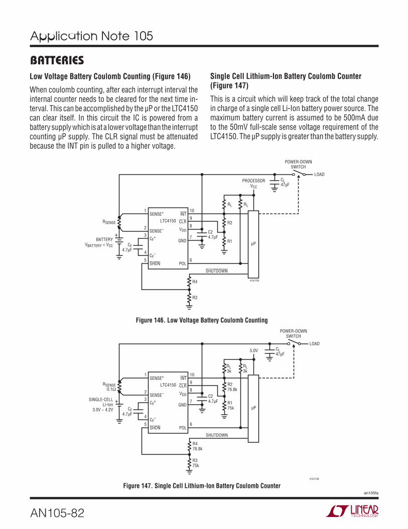
Application Note 105
AN105-82
an105fa
Low Voltage Battery Coulomb Counting (Figure 146)
When coulomb counting, after each interrupt interval the internal counter needs to be cleared for the next time in-terval. This can be accomplished by the µP or the LTC4150 can clear itself. In this circuit the IC is powered from a battery supply which is at a lower voltage than the interrupt counting µP supply. The CLR signal must be attenuated because the INT pin is pulled to a higher voltage.
INTSENSE+
SENSE–
SHDN
SHUTDOWN
R4
R3
CLR
POL
LTC4150
µP
C24.7µF
RL10
9
8
7
6
1
2
5
4150 F06
VDD
GND
RL
PROCESSORVCC
POWER-DOWNSWITCH
CL47µF
LOAD
+CF
+
CF–
3
4
CF4.7µF
BATTERYVBATTERY < VCC
RSENSE R2
R1
INTSENSE+
SENSE–
SHDN
SHUTDOWN
R476.8k
R375k
CLR
POL
LTC4150
µP
C24.7µF
RL3k
10
9
8
7
6
1
2
5
4150 F08
VDD
GND
RL3k
5.0V
POWER-DOWNSWITCH
CL47µF
LOAD
CF+
CF–
3
4
CF4.7µF
SINGLE-CELLLi-Ion
3.0V ~ 4.2V
RSENSE0.1Ω
R276.8k
R175k
+
Single Cell Lithium-Ion Battery Coulomb Counter (Figure 147)
This is a circuit which will keep track of the total change in charge of a single cell Li-Ion battery power source. The maximum battery current is assumed to be 500mA due to the 50mV full-scale sense voltage requirement of the LTC4150. The µP supply is greater than the battery supply.
Figure 146. Low Voltage Battery Coulomb Counting
Figure 147. Single Cell Lithium-Ion Battery Coulomb Counter
BATTERIES
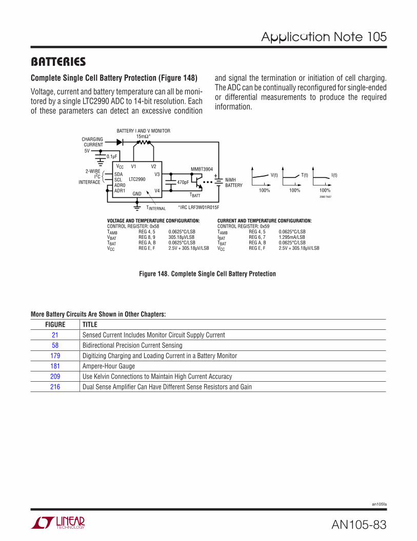
Application Note 105
AN105-83
an105fa
VCC V1
LTC2990
BATTERY I AND V MONITOR15mΩ*CHARGING
CURRENT
2-WIREI2C
INTERFACE
5V
GND
470pF NiMHBATTERY
V(t)
100% 100%
• • •
TBATT
MMBT3904SDASCLADR0ADR1
V3
V4
V2
2990 TA07
TINTERNAL *IRC LRF3W01R015F
CURRENT AND TEMPERATURE CONFIGURATION:CONTROL REGISTER: 0x59TAMB REG 4, 5 0.0625°C/LSBIBAT REG 6, 7 1.295mA/LSBTBAT REG A, B 0.0625°C/LSBVCC REG E, F 2.5V + 305.18µV/LSB
VOLTAGE AND TEMPERATURE CONFIGURATION:CONTROL REGISTER: 0x58TAMB REG 4, 5 0.0625°C/LSBVBAT REG 8, 9 305.18µVLSBTBAT REG A, B 0.0625°C/LSBVCC REG E, F 2.5V + 305.18µV/LSB
+ T(t)
100%
I(t)
0.1µF
Complete Single Cell Battery Protection (Figure 148)
Voltage, current and battery temperature can all be moni-tored by a single LTC2990 ADC to 14-bit resolution. Each of these parameters can detect an excessive condition
and signal the termination or initiation of cell charging. The ADC can be continually reconfigured for single-ended or differential measurements to produce the required information.
Figure 148. Complete Single Cell Battery Protection
BATTERIES
More Battery Circuits Are Shown in Other Chapters:FIGURE TITLE
21 Sensed Current Includes Monitor Circuit Supply Current58 Bidirectional Precision Current Sensing179 Digitizing Charging and Loading Current in a Battery Monitor181 Ampere-Hour Gauge209 Use Kelvin Connections to Maintain High Current Accuracy216 Dual Sense Amplifier Can Have Different Sense Resistors and Gain
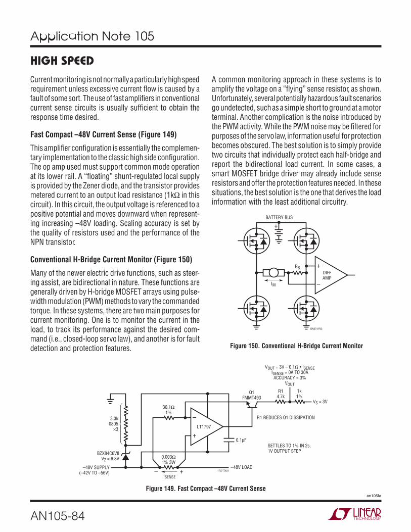
Application Note 105
AN105-84
an105fa
Current monitoring is not normally a particularly high speed requirement unless excessive current flow is caused by a fault of some sort. The use of fast amplifiers in conventional current sense circuits is usually sufficient to obtain the response time desired.
Fast Compact –48V Current Sense (Figure 149)
This amplifier configuration is essentially the complemen-tary implementation to the classic high side configuration. The op amp used must support common mode operation at its lower rail. A “floating” shunt-regulated local supply is provided by the Zener diode, and the transistor provides metered current to an output load resistance (1kΩ in this circuit). In this circuit, the output voltage is referenced to a positive potential and moves downward when represent-ing increasing –48V loading. Scaling accuracy is set by the quality of resistors used and the performance of the NPN transistor.
Conventional H-Bridge Current Monitor (Figure 150)
Many of the newer electric drive functions, such as steer-ing assist, are bidirectional in nature. These functions are generally driven by H-bridge MOSFET arrays using pulse-width modulation (PWM) methods to vary the commanded torque. In these systems, there are two main purposes for current monitoring. One is to monitor the current in the load, to track its performance against the desired com-mand (i.e., closed-loop servo law), and another is for fault detection and protection features.
A common monitoring approach in these systems is to amplify the voltage on a “flying” sense resistor, as shown. Unfortunately, several potentially hazardous fault scenarios go undetected, such as a simple short to ground at a motor terminal. Another complication is the noise introduced by the PWM activity. While the PWM noise may be filtered for purposes of the servo law, information useful for protection becomes obscured. The best solution is to simply provide two circuits that individually protect each half-bridge and report the bidirectional load current. In some cases, a smart MOSFET bridge driver may already include sense resistors and offer the protection features needed. In these situations, the best solution is the one that derives the load information with the least additional circuitry.
–
+LT1797
0.1µF
R1 REDUCES Q1 DISSIPATION
Q1FMMT493
0.003Ω1% 3W
BZX84C6V8VZ = 6.8V
–48V SUPPLY(–42V TO –56V)
3.3k0805
×3
30.1Ω1%
ISENSE+–
R14.7k
VS = 3V
1k1%
VOUT = 3V – 0.1Ω • ISENSEISENSE = 0A TO 30AACCURACY ≈ 3%
–48V LOAD1797 TA01
SETTLES TO 1% IN 2s,1V OUTPUT STEP
VOUT
Figure 149. Fast Compact –48V Current Sense
–
+
+
IM
RS
BATTERY BUS
DIFFAMP
DN374 F03
Figure 150. Conventional H-Bridge Current Monitor
HIGH SPEED

Application Note 105
AN105-85
an105fa
Single-Supply 2.5V Bidirectional Operation with External Voltage Reference and I/V Converter (Figure 151)
The LT1787’s output is buffered by an LT1495 rail-to-rail op amp configured as an I/V converter. This configuration is ideal for monitoring very low voltage supplies. The LT1787’s VOUT pin is held equal to the reference voltage appearing at the op amp’s non-inverting input. This al-lows one to monitor supply voltages as low as 2.5V. The op amp’s output may swing from ground to its positive supply voltage. The low impedance output of the op amp
Figure 151. Single-Supply 2.5V Bidirectional Operation with External Voltage Reference and I/V Converter
2.5V
C11µF
RSENSEISENSE
2.5V + VSENSE(MAX)
TOCHARGER/
LOAD
VOUT A
1M5%
1787 F07
LT1495
C31000pF
LT1389-1.25
2.5V +
–A1
1
2
3
4
8
7
6
5
LT1787FIL+FIL–
VBIAS
VOUT
VS– VS
+
DNC
VEE
ROUT
may drive following circuitry more effectively than the high output impedance of the LT1787. The I/V converter configuration also works well with split supply voltages.
Battery Current Monitor (Figure 152)
One LT1495 dual op amp package can be used to establish separate charge and discharge current monitoring outputs. The LT1495 features Over-the-Top operation allowing the battery potential to be as high as 36V with only a 5V amplifier supply voltage.
Figure 152. Battery Current Monitor
–
+
–
+
1495 TA05
RSENSE0.1Ω
ILCHARGE
RA
2N3904
VO = IL RSENSE
FOR RA = 1k, RB = 10k
= 1V/A
CHARGEOUT
DISCHARGEOUT
DISCHARGE
2N3904
RA
RA RA
RB
RBRA
VOIL
RB
A11/2 LT1495
5V 12V
A21/2 LT1495
( )
HIGH SPEED

Application Note 105
AN105-86
an105fa
Figure 153. Fast Current Sense with Alarm Figure 154. Fast Differential Current Source
Fast Current Sense with Alarm (Figure 153)
The LT1995 is shown as a simple unity gain difference amplifier. When biased with split supplies the input current can flow in either direction providing an output voltage of 100mV/A from the voltage across the 100mΩ sense resis-tor. With 32MHz of bandwidth and 1000V/µs slew rate the response of this sense amplifier is fast. Adding a simple comparator with a built in reference voltage circuit such as the LT6700-3 can be used to generate an overcurrent flag. With the 400mV reference the flag occurs at 4A.
LT1995G = 1
SENSEOUTPUT100mV/A
FLAGOUTPUT4A LIMIT
15V15V TO –15V
0.1Ω
I
10k
1995 TA05
10kLT6700-3
–
+
400mV
–15V
REF
P1
M1
LT1022 • TA07
6
10pF15V
–15V
3
2 7
4
LT1022
+
–VIN1
RLIOUT
IOUT =VIN2 – VIN1
VIN2
R* R*
R*
R*
R
2IOUTP-P • RL
*MATCH TO 0.01% FULL-SCALE POWER BANDWIDTH = 1MHz FOR IOUTR = 8VP-P = 400kHz FOR IOUTR = 20VP-P MAXIMUM IOUT = 10mAP-P COMMON MODE VOLTAGE AT LT1022 INPUT =
Fast Differential Current Source (Figure 154)
This is a variation on the Howland configuration, where load current actually passes through a feedback resistor as an implicit sense resistance. Since the effective sense resistance is relatively large, this topology is appropriate for producing small controlled currents.
HIGH SPEED
More High Speed Circuits Are Shown in Other Chapters:FIGURE TITLE
22 Wide Voltage Range Current Sensing124 Monitor H-Bridge Motor Current Directly128 Fixed Gain DC Motor Current Monitor143 Battery Stack Monitoring168 Monitoring a Fuse Protected Circuit169 Circuit Fault Protection with Early Warning and Latching Load Disconnect170 Use Comparator Output to Initialize Interrupt Routines

Application Note 105
AN105-87
an105fa
The lack of current flow or the dramatic increase of current flow very often indicates a system fault. In these circuits it is important to not only detect the condition, but also ensure the safe operation of the detection circuitry itself. System faults can be destructive in many unpredictable ways.
High Side Current Sense and Fuse Monitor (Figure 155)
The LT6100 can be used as a combination current sen-sor and fuse monitor. This part includes on-chip output buffering and was designed to operate with the low supply voltage (≥2.7V), typical of vehicle data acquisition systems, while the sense inputs monitor signals at the higher bat-tery bus potential. The LT6100 inputs are tolerant of large input differentials, thus allowing the blown-fuse operating condition (this would be detected by an output full-scale indication). The LT6100 can also be powered down while maintaining high impedance sense inputs, drawing less than 1µA max from the battery bus.
Additional Resistor R3 Protects Output During Supply Reversal (Figure 157)
If the output of the LTC6101 is wired to an independently powered device that will effectively short the output to another rail or ground (such as through an ESD protection clamp) during a reverse supply condition, the LTC6101’s output should be connected through a resistor or Schottky diode to prevent excessive fault current.
Electronic Circuit Breaker (Figure 158)
The LT1620l current sense amplifier is used to detect an overcurrent condition and shut off a P-MOSFET load switch. A fault flag is produced in the overcurrent condition and a self-reset sequence is initiated.
OUTPUT2.5V = 25AVEE
OUT
DN374 F02
RSENSE2mΩ FUSE
LT6100
81
VS– VS
+
BATTERYBUS
A4ADC
POWER≥2.7V
2VCC
A23
4
7
C20.1µF
6
5
FIL
TO LOAD
– +
+
Figure 155. High Side Current Sense and Fuse Monitor
Figure 156. Schottky Prevents Damage During Supply Reversal
Figure 157. Additional Resistor R3 Protects Output During Supply Reversal
Schottky Prevents Damage During Supply Reversal (Figure 156)
The LTC6101 is not protected internally from external reversal of supply polarity. To prevent damage that may occur during this condition, a Schottky diode should be added in series with V–. This will limit the reverse current through the LTC6101. Note that this diode will limit the low voltage performance of the LTC6101 by effectively reducing the supply voltage to the part by VD.
6101 F07
LTC6101
R24.99k
D1
R1100
VBATT
52
1
34
RSENSE
LOAD
–+
6101 F08
ADCLTC6101
R24.99k
D1
R1100 VBATT
R31k
52
1
34
RSENSE
LOAD
–+
FAULT SENSING

Application Note 105
AN105-88
an105fa
Electronic Circuit Breaker (Figure 159)
The LTC1153 is an electronic circuit breaker. Sensed cur-rent to a load opens the breaker when 100mV is developed between the supply input, VS, and the drain sense pin, DS. To avoid transient, or nuisance trips of the break compo-nents RD and CD delay the action for 1ms. A thermistor can also be used to bias the shutdown input to monitor heat generated in the load and remove power should the temperature exceed 70°C in this example. A feature of the LTC1153 is timed automatic reset which will try to reconnect the load after 200ms using the 0.22μF timer capacitor shown.
1.25V Electronic Circuit Breaker (Figure 160)
The LTC4213 provides protection and automatic circuit breaker action by sensing drain-to-source voltage drop across the N-MOSFET. The sense inputs have a rail-to-rail common mode range, so the circuit breaker can protect bus voltages from 0V up to 6V. Logic signals flag a trip condition (with the READY output signal) and reinitialize the breaker (using the ON input). The ON input may also be used as a command in a “smart switch” application.
Figure 158. Electronic Circuit Breaker
Figure 159. Electronic Circuit Breaker
Figure 160. 1.25V Electronic Circuit Breaker
AVG
PROG
VCC
+IN
SENSE
LT1620MS8
1
2
3
4
8
7IOUT
GND
–IN
6
5
4.7k 33k
100k
33k
CDELAY
0.1µF5V
0.033Ω 5V AT 1APROTECTED
FAULT
LT1620/21 • TA03
1N4148
2N3904
1k
2N3904
Si9434DY
100Ω
TYPICAL DC TRIP AT 1.6A3A FAULT TRIPSIN 2ms WITH CDELAY = 1.0µF
IN
CT
STATUS
GND
VS
DS
G
SHUTDOWN
LTC1153
CD0.01µF
RD100k
*RSEN 0.1Ω
IRLR024
51k
SENSITIVE5V LOAD
**70°CPTC
51k
5V
TO µP
CT0.22µF
ON/OFF
ALL COMPONENTS SHOWN ARE SURFACE MOUNT.IMS026 INTERNATIONAL MANUFACTURING SERVICE, INC. (401) 683-9700RL2006-100-70-30-PT1 KEYSTONE CARBON COMPANY (814) 781-1591
***
LTC1153 • TA01
Z5U
OFF ON
LTC4213
VCC
ON READY
10k
ISELGND
GATE
SI4864DY
VBIAS
VOUT1.25V3.5A
VIN1.25V
VBIAS2.3V TO 6V
SENSENSENSEP
4213 TA01
FAULT SENSING

Application Note 105
AN105-89
an105fa
Lamp Outage Detector (Figure 161)
In this circuit, the lamp is monitored in both the on and off condition for continuity. In the off condition, the filament pull-down action creates a small test current in the 5kΩ that is detected to indicate a good lamp. If the lamp is open, the 100kΩ pull-up, or the relay contact, provides the op amp bias current through the 5kΩ, that is opposite in polarity. When the lamp is powered and filament current is flowing, the drop in the 0.05Ω sense resistor will exceed that of the 5kΩ and a lamp-good detection will still occur. This circuit requires particular Over-the-Top input characteristics for
–
+LT1637
5k
1M5V TO 44V 3V
100k
0.5Ω
LAMPON/OFF
OUT
1637 TA05
OUT = 0V FOR GOOD BULB 3V FOR OPEN BULB
MOC207
MOC207
MOC207
FUSESTATUS
SUPPLY ASTATUS
5V47k
5V47k
5V47k
R347k1/4W
SUPPLY BSTATUS
OK: WITHIN SPECIFICATIONOV: OVERVOLTAGEUV: UNDERVOLTAGE
–48V OUT
= LOGIC COMMON
0: LED/PHOTODIODE ON1: LED/PHOTODIODE OFF*IF BOTH FUSES (F1 AND F2) ARE OPEN, ALL STATUS OUTPUTS WILL BE HIGH SINCE R3 WILL NOT BE POWERED
OUT F
–48VRETURN
VA
3
4
57
2
8
1
6
VB
FUSE A
F1 D1
D2F2
RTN
LTC1921
FUSE B OUT A
OUT B
SUPPLY A–48V
SUPPLY B–48V
R1100k
R2100k
SUPPLY ASTATUS
0011
VBOK
UV OR OVOK
UV OR OV
VAOKOK
UV OR OVUV OR OV
SUPPLY BSTATUS
0101
FUSE STATUS011
1*
VFUSE B= VB≠ VB= VB≠ VB
VFUSE A= VA= VA≠ VA≠ VA
the op amp, so part substitutions are discouraged (how-ever, this same circuit also works properly with an LT1716 comparator, also an Over-the-Top part).
Simple Telecom Power Supply Fuse Monitor (Figure 162)
The LTC1921 provides an all-in-one telecom fuse and supply-voltage monitoring function. Three opto-isolated status flags are generated that indicate the condition of the supplies and the fuses.
Conventional H-Bridge Current Monitor (Figure 163)
Many of the newer electric drive functions, such as steer-ing assist, are bidirectional in nature. These functions are generally driven by H-bridge MOSFET arrays using pulse-width modulation (PWM) methods to vary the commanded torque. In these systems, there are two main purposes for current monitoring. One is to monitor the current in the load, to track its performance against the desired com-mand (i.e., closed-loop servo law), and another is for fault detection and protection features.
Figure 161. Lamp Outage Detector
Figure 162. Simple Telecom Power Supply Fuse Monitor
FAULT SENSING

Application Note 105
AN105-90
an105fa
Figure 163. Conventional H-Bridge Current Monitor
Figure 164. Single-Supply 2.5V Bidirectional Operation with External Voltage Reference and I/V Converter
Figure 165. Battery Current Monitor
A common monitoring approach in these systems is to amplify the voltage on a “flying” sense resistor, as shown. Unfortunately, several potentially hazardous fault scenarios go undetected, such as a simple short to ground at a motor terminal. Another complication is the noise introduced by the PWM activity. While the PWM noise may be filtered for purposes of the servo law, information useful for protection becomes obscured. The best solution is to simply provide two circuits that individually protect each half-bridge and report the bidirectional load current. In some cases, a smart MOSFET bridge driver may already include sense resistors and offer the protection features needed. In these situations, the best solution is the one that derives the load information with the least additional circuitry.
–
+
+
IM
RS
BATTERY BUS
DIFFAMP
DN374 F03
Single-Supply 2.5V Bidirectional Operation with External Voltage Reference and I/V Converter (Figure 164)
The LT1787’s output is buffered by an LT1495 rail-to-rail op amp configured as an I/V converter. This configuration is ideal for monitoring very low voltage supplies. The LT1787’s VOUT pin is held equal to the reference voltage appearing at the op amp’s non-inverting input. This al-lows one to monitor supply voltages as low as 2.5V. The op amp’s output may swing from ground to its positive supply voltage. The low impedance output of the op amp may drive following circuitry more effectively than the high output impedance of the LT1787. The I/V converter configuration also works well with split supply voltages.
2.5V
C11µF
RSENSEISENSE
2.5V + VSENSE(MAX)
TOCHARGER/
LOAD
VOUT A
1M5%
1787 F07
LT1495
C31000pF
LT1389-1.25
2.5V +
–A1
1
2
3
4
8
7
6
5
LT1787FIL+FIL–
VBIAS
VOUT
VS– VS
+
DNC
VEE
ROUT
Battery Current Monitor (Figure 165)
One LT1495 dual op amp package can be used to establish separate charge and discharge current monitoring outputs. The LT1495 features Over-the-Top operation allowing the battery potential to be as high as 36V with only a 5V amplifier supply voltage.
–
+
–
+
1495 TA05
RSENSE0.1Ω
ILCHARGE
RA
2N3904
VO = IL RSENSE
FOR RA = 1k, RB = 10k
= 1V/A
CHARGEOUT
DISCHARGEOUT
DISCHARGE
2N3904
RA
RA RA
RB
RBRA
VOIL
RB
A11/2 LT1495
5V 12V
A21/2 LT1495
( )
FAULT SENSING

Application Note 105
AN105-91
an105fa
Fast Current Sense with Alarm (Figure 166)
The LT1995 is shown as a simple unity gain difference amplifier. When biased with split supplies the input current can flow in either direction providing an output voltage of 100mV/A from the voltage across the 100mΩ sense resis-tor. With 32MHz of bandwidth and 1000V/µs slew rate the response of this sense amplifier is fast. Adding a simple comparator with a built in reference voltage circuit such as the LT6700-3 can be used to generate an overcurrent flag. With the 400mV reference the flag occurs at 4A.
LT1995G = 1
SENSEOUTPUT100mV/A
FLAGOUTPUT4A LIMIT
15V15V TO –15V
0.1Ω
I
10k
1995 TA05
10kLT6700-3
–
+
400mV
–15V
REF
P1
M1
Figure 166. Fast Current Sense with Alarm
Figure 167. Monitor Current in an Isolated Supply Line
Figure 168. Monitoring a Fuse Protected Circuit
Monitor Current in an Isolated Supply Line (Figure 167)
Using the current sense amplifier output current to directly modulate the current in a photo diode is a simple method to monitor an isolated 48V industrial/telecom power supply. Current faults can be signaled to nonisolated monitoring circuitry.
Monitoring a Fuse Protected Circuit (Figure 168)
Current sensing a supply line that has a fuse for overcurrent protection requires a current sense amplifier with a wide differential input voltage rating. Should the fuse blow open the full load supply voltage appears across the inputs to the sense amplifier. The LT6105 can work with input voltage differentials up to 44V. The LT6105 output slews at 2V/µs so can respond quickly to fast current changes. When the fuse opens the LT6105 output goes high and stays there.
6103 TA07
1/2LTC6103
RIN
V–
VSENSE
RSENSE
ISENSE
LOAD
VOUT = VLOGIC – ISENSE • • N • ROUTRSENSE
RIN
N = OPTO-ISOLATOR CURRENT GAIN
VS
ANY OPTO-ISOLATOR
ROUT
VOUT
VLOGIC
V+V–
OUT
–IN +IN
+
+
–
–
OUTPUTOUT
6105 F03
RSENSE FUSE
LT6105
VS– VS
+
V–
V+
C20.1µF
C10.1µF
DC SOURCE (≤ 44V)
5V
TO LOAD
– +
+
–IN +IN
RIN2
ROUT
RIN1
FAULT SENSING

Application Note 105
AN105-92
an105fa
Circuit Fault Protection with Early Warning and Latching Load Disconnect (Figure 169)
With a precision current sense amplifier driving two built in comparators, LT6109-2 can provide current overload protection to a load circuit. The internal comparators have a fixed 400mV reference. The current sense output is resistor divided down so that one comparator will trip at an early warning level and the second at a danger level of current to the load (100mA and 250mA in this example). The comparator outputs latch when tripped so they can be used as a circuit breaker to disconnect and protect the load until a reset pulse is provided.
Use Comparator Output to Initialize Interrupt Routines (Figure 170)
The comparator outputs can connect directly to I/O or interrupt inputs to any microcontroller. A low level at OUTC2 can indicate an undercurrent condition while a low level at OUTC1 indicates an overcurrent condition. These interrupts force service routines in the microcontroller.
Figure 169. Circuit Fault Protection with Early Warning and Latching Load Disconnect
Figure 170. Use Comparator Output to Initialize Interrupt Routines
FAULT SENSING
SENSEHI SENSELO
OUTALT6109-2
INC2RESET
INC12N2700
100mA WARNING
250mA DISCONNECT
V+
EN/RST
OUTC1
OUTC2
V–
0.1Ω IRF9640
3.3V6.2V
12V
100Ω
6.04k100k1.62k10k
1k
1k
10µF
VOUT
2.37k
1.6k
610912 TA01a
TO LOAD
SENSEHI SENSELO
OUTA
0.1ΩV+
100Ω
LT6109-1
V–
TO LOADEXAMPLE
VOUTADC IN
2k
6.65kINC2
1.33k
INC1
V+
EN/RST
OUTC1
8
1
7
6
5
OUTC2
10
9
10k 2
5V
4
3
RESET
6109 TA03
10k
5V
VOUT/ADC IN
AtMega1280PB0
PB1
PCINT2
PCINT3
ADC2
PB5
5
6
7
2
3
1
UNDERCURRENT ROUTINE
RESET COMPARATORS
MCU INTERUPT
OUTC2 GOES LOW5V

Application Note 105
AN105-93
an105fa
Current Sense with Overcurrent Latch and Power-On Reset with Loss of Supply (Figure 171)
The LT6801-2 has a normal nonlatching comparator built in. An external logic gate configured in a positive feedback
arrangement can create a latching output when an over-current condition is sensed. The same logic gate can also generate an active low power-on reset signal.
Figure 171. Current Sense with Overcurrent Latch and Power-On Reset with Loss of Supply
–
+
V+
V–
V–
4
610812 TA06
V+
400mVREFERENCE
V+
RIN100Ω
RSENSE
ILOAD
OUTA 6
INC 5 VTH
7
SENSEHI
LT6108-2
5V
SENSELO
OUTC
8
1
3
R79.53k
R8499Ω
R124.9k
R2200k
VDD
R61M
*OPTIONAL COMPONENT
C10.1µF
Q1*2N2222 R4*
3.4k
R5*100k
R9*30k
R310k
–
+
FAULT SENSING

Application Note 105
AN105-94
an105fa
FAULT SENSINGMore Fault Sensing Circuits Are Shown in Other Chapters:
FIGURE TITLE120 Bidirectional Current Sensing in H-Bridge Drivers125 Large Input Voltage Range for Fused Solenoid Current Monitoring136 Coulomb Counting Battery Gas Gauge143 Battery Stack Monitoring145 High Voltage Battery Coulomb Counting146 Low Voltage Battery Coulomb Counting147 Single Cell Lithium-Ion Battery Coulomb Counter211 Power Intensive Circuit Board Monitoring
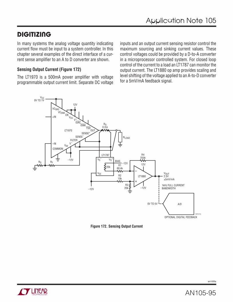
Application Note 105
AN105-95
an105fa
In many systems the analog voltage quantity indicating current flow must be input to a system controller. In this chapter several examples of the direct interface of a cur-rent sense amplifier to an A to D converter are shown.
Sensing Output Current (Figure 172)
The LT1970 is a 500mA power amplifier with voltage programmable output current limit. Separate DC voltage
inputs and an output current sensing resistor control the maximum sourcing and sinking current values. These control voltages could be provided by a D-to-A converter in a microprocessor controlled system. For closed loop control of the current to a load an LT1787 can monitor the output current. The LT1880 op amp provides scaling and level shifting of the voltage applied to an A-to-D converter for a 5mV/mA feedback signal.
VCSRC
COMMONVEE
VCSNK
V–FILTER
V+
12V
ENVCC
ISNKISRC
SENSE–SENSE+
TSDOUT
+IN
VCC0V TO 1V
LT1970
–12V
–IN
RS0.2Ω
RLOAD
1970 F10
RG RFVS
–
VEE
20k
BIAS–12V
–12V
R160.4k
R4255k
VOUT2.5V±5mV/mA
1kHz FULL CURRENTBANDWIDTH
R210k
R320k
VS+
LT1787
–
+LT1880
12V
–12V
0V TO 5V A/D
OPTIONAL DIGITAL FEEDBACK
Figure 172. Sensing Output Current
DIGITIZING

Application Note 105
AN105-96
an105fa
Split or Single-Supply Operation, Bidirectional Output into A/D (Figure 173)
In this circuit, split supply operation is used on both the LT1787 and LT1404 to provide a symmetric bidirectional measurement. In the single-supply case, where the LT1787 Pin 6 is driven by VREF, the bidirectional measurement range is slightly asymmetric due to VREF being somewhat greater than midspan of the ADC input range.
1Ω1%
VEE–5V
VOUT (±1V)
VSRCE≈4.75V
IS = ±125mA
1
2
3
4
8
7
6
5
LT1787FIL+FIL–
VBIAS
VOUT
VS– VS
+
DNC
VEE
20k
1787 TA02
10µF16V
7
6
8
5
4
3
2
1
VREFGND
LTC1404
CONV
CLK
DOUT
AIN
VCC5V
VEE–5V
DOUT
OPTIONAL SINGLESUPPLY OPERATION:
DISCONNECT VBIASFROM GROUND
AND CONNECT IT TO VREF.REPLACE –5V SUPPLY
WITH GROUND.OUTPUT CODE FOR ZEROCURRENT WILL BE ~2430
10µF16V
10µF16V
CLOCKINGCIRCUITRY
TO µP
6101 TA06
LTC2433-1
LTC6101
ROUT4.99k
RIN100Ω
VOUT
VSENSEILOAD
4V TO 60V
1µF5V
LOAD
–+
– +
VOUT = • VSENSE = 49.9VSENSEROUTRIN
ADC FULL-SCALE = 2.5V
2 1
9
8
7
1063
4
5
VCCSCK
REF+
REF– GND
IN+
IN– CCFO
SDD
52
1
34
16-Bit Resolution Unidirectional Output into LTC2433 ADC (Figure 174)
The LTC2433-1 can accurately digitize signal with source impedances up to 5kΩ. This LTC6101 current sense circuit uses a 4.99kΩ output resistance to meet this requirement, thus no additional buffering is necessary.
Figure 173. Split or Single-Supply Operation, Bidirectional Output into A/D
Figure 174. 16-Bit Resolution Unidirectional Output into LTC2433 ADC
DIGITIZING

Application Note 105
AN105-97
an105fa
Figure 175. 12-Bit Resolution Unidirectional Output into LTC1286 ADC
Figure 176. Directly Digitize Current with 16-Bit Resolution
12-Bit Resolution Unidirectional Output into LTC1286 ADC (Figure 175)
While the LT1787 is able to provide a bidirectional output, in this application the economical LTC1286 is used to digitize a unidirectional measurement. The LT1787 has a nominal gain of eight, providing a 1.25V full-scale output at approximately 100A of load current.
1 8
2 7
3 6
4 5
LT1787HV
RSENSE0.0016Ω
1787 TA01
C11µF 5V
FIL+FIL–
R115k
C20.1µFVOUT = VBIAS + (8 • ILOAD • RSENSE)
I = 100A
2.5V TO 60V
TOLOAD
LT1634-1.25
TO µP
VREF VCC
GND
LTC1286CS
CLKDOUT
+IN
–IN
VBIAS
VOUT
ROUT20k
VS– VS
+
DNC
VEE
TO µP
6102 TA05
LTC2433-1
LTC6102-1
ROUT4.99k
RIN100Ω
VOUT
VSENSE
ILOAD
4V TO 60V
POWER ENABLE
1µF5V
LOAD
–+
–+
VOUT = • VSENSE = 49.9VSENSEROUTRIN
ADC FULL-SCALE = 2.5V
2 1
9
8
7
1063
4
5
VCCSCK
REF+
REF– GND
IN+
IN– CCFO
SDD
V+V–
EN
OUT
–INS+IN
–INF
VREG0.1µF
Directly Digitize Current with 16-Bit Resolution (Figure 176)
The low offset precision of the LTC6102 permits direct digitization of a high side sensed current. The LTC2433 is a 16-bit delta sigma converter with a 2.5V full-scale range. A resolution of 16 bits has an LSB value of only 40µV. In this circuit the sense voltage is amplified by a factor of 50. This translates to a sensed voltage resolution of only 0.8µV per count. The LTC6102 DC offset typically contributes only four LSB’s of uncertainty.
DIGITIZING

Application Note 105
AN105-98
an105fa
Directly Digitizing Two Independent Currents (Figure 177)
With two independent current sense amplifiers in the LTC6103, two currents from different sources can be simultaneously digitized by a 2-channel 16-bit ADC such as the LTC2436-1. While shown to have the same gain on each channel, it is not necessary to do so. Two different current ranges can be gain scaled to match the same full-scale range for each ADC channel.
Digitize a Bidirectional Current Using a Single-Sense Amplifier and ADC (Figure 178)
The dual LTC6104 can be connected in a fashion to source or sink current at its output depending on the direction of current flow through the sense resistor. Biasing the amplifier output resistor and the VREF input of the ADC to an external 2.5V LT1004 voltage reference allows a 2.5V full-scale input voltage to the ADC for current flowing in either direction.
Figure 177. Directly Digitizing Two Independent Currents
Figure 178. Digitize a Bidirectional Current Using a Single-Sense Amplifier and ADC
DIGITIZING
+ – +–
8 7 6 5
241
+INA
OUTA OUTB
VSBVSA
LTC6103
62
13
12
11
1
1µF5V
5
7
4 TO µP
6103 TA01a
–INA –INB
RIN100Ω
RIN100Ω
VSENSE VSENSE+ + ––
VA+ VB
+
+INB
V–
ROUT4.99k
ROUT4.99k
LOADLOAD
ILOAD ILOAD
LTC2436-1
CH1
CH0
3,8,9,10,14,15,16
+ –
8 7 6
4
+INA
OUT
VSVS
A
LTC6104
12V
TO µP
6104 TA01a
–INA –INB
RIN100Ω
RIN100Ω
TOCHARGER/LOAD RSENSE
VSENSE
VREF
+–
+INB
V–
VREF+IN
5V
–INLT1004-2.5
C20.1µF
R12.3k
VCC
LTC1286
GND
ILOAD
+
CURRENTMIRROR
+–
5
B
CS
CLK
DOUTROUT2.5k
+C11µF
1

Application Note 105
AN105-99
an105fa
Digitizing Charging and Loading Current in a Battery Monitor (Figure 179)
A 16-bit digital output battery current monitor can be implemented with just a single sense resistor, an LT1999 and an LTC2344 delta sigma ADC. With a fixed gain of ten and DC biased output the digital code indicates the instantaneous loading or charging current (up to 10A) of a system battery power source.
Figure 179. Digitizing Charging and Loading Current in a Battery Monitor
Figure 180. Complete Digital Current Monitoring
1999 TA02
5V 0.1µF
LT1999-10
4k
0.8k
160k
160k
2µA
0.8k4k
V+
+–
SHDN
+–
VOUT
40k
VREF
VSHDN
V+
V+
V+
V+
4
0.1µF
5V
CHARGER
LOAD
0.025Ω
BAT42V
VCC VREF
0.1µF
+IN
10µF
CS
SCK
SDO
LTC2433-1VOUT
+
–
5V
–IN
0.1µF
2
3
1
5
7
6
8
V+IN
V–IN
Complete Digital Current Monitoring (Figure 180)
An LTC2470 16-bit delta sigma A-to-D converter can directly digitize the output of the LT6109 representing a circuit load current. At the same time the comparator outputs connect to MCU interrupt inputs to immediately signal programmable threshold over and undercurrent conditions.
SENSEHI SENSELO
OUTA
0.1ΩSENSELOW
SENSEHIGH
LT6109-1
V–
OUT
2k0.1µF
0.1µF
6.65k
INC2
1.33k
OVERCURRENT
UNDERCURRENT
INC1
V+
EN/RST
OUTC1
8
1
7
6
5
OUTC2
10
9
2
4
VCC
VCC VREF
10k3
RESET
6109 TA05
IN
VCC
10k
IN+ LTC2470
COMP
TOMCU
100Ω
DIGITIZING

Application Note 105
AN105-100
an105fa
Ampere-Hour Gauge (Figure 181)
With specific scaling of the current sense resistor, the LTC4150 can be set to output exactly 10,000 interrupt pulses for one Amp-hr of charge drawn from a battery source. With such a base-10 round number of pulses a series of decade counters can be used to create a visual 5-digit display. This schematic is just the concept. The polarity output can be used to direct the interrupt pulses to either the count-up or count-down clock input to display total net charge.
Power Sensing with Built-In A-to-D Converter (Figure 182)
The LTC4151 contains a dedicated current sense input channel to a 3-channel 12-bit delta-sigma ADC. The ADC directly and sequentially measures the supply voltage (102V full-scale), supply current (82mV full-scale) and a separate analog input channel (2V full-scale). The 12-bit resolution data for each measurement is output through an I2C link.
1.1Ω1.2Ω 100mΩ
SENSE RESISTANCE = 0.0852ΩIMAX = 588mA10,000 PULSES = 1Ah
+
INTSENSE+
SENSE–
CLR
4150 F09
LTC4150CD40110B
CD40110B
CD40110B
CD40110B
CD40110B
LOADCHARGER
4151 TA01
3.3V
0.02Ω
µCONTROLLER
LTC4151SHDN
VIN7V to 80V VOUT
VIN
VDD
MEASUREDVOLTAGE
SCL
SDA
ADIN
ADR1
SCL
2k 2k
SDA
ADR0GND
SENSE+ SENSE–
Figure 181. Ampere-Hour Gauge
Figure 182. Power Sensing with Built-In A-to-D Converter
DIGITIZING

Application Note 105
AN105-101
an105fa
Figure 183. Isolated Power Measurement
Figure 184. Fast Data Rate Isolated Power Measurement
Isolated Power Measurement (Figure 183)
With separate data input and output pins, it is a simple matter to fully isolate the LTC4151-1/LTC4151-2 from a controller system. The supply voltage and operating current of the isolated system is digitized and conveyed through three opto-isolators.
Fast Data Rate Isolated Power Measurement (Figure 184)
With separate data input and output pins, it is a simple matter to fully isolate the LTC4151-1/LTC4151-2 from a controller system. The supply voltage and operating current of the isolated system is digitized and conveyed through three high speed opto-isolators.
4151 F09
3.3VRS0.02Ω
µ-CONTROLLER
LTC4151-1
SCL
SCL
VIN48V
VINVDD
VADIN
SDAI
ADIN
ADR1
R50.51k
R610k
R710k
R40.51k
R120k
R220k
R35.1k
18
2736
45
81
7263
54
SDA
ADR0
GND
SENSE+ SENSE–
SDA0
MOCD207M
MOCD207M
ADINADIN
R10.02Ω
LTC4151-2
VIN7V to 80V VOUT
VCC8
5V
1
2
8
7
6
5
1
2
3
4
ISO_SDA
ISO_SCL
7
5GND4
1
2
8
5C71µF100V
VIN
VIN
ADR1
ADR0
SDAO
INLT3010-5
SHDN
OUT
SENSEGND
SDAI
SCLGND
SENSE+ SENSE–
C61µF
ISO1PS9817-2
ISO2PS9817-2
R310k
R410k
R111k
R1310k
4151 F11
R121k
R1410k
R81k
C40.1µF
VCC
GND
DIGITIZING

Application Note 105
AN105-102
an105fa
Adding Temperature Measurement to Supply Power Measurement (Figure 185)
One use for the spare analog input of the LTC4151 could be to measure temperature. This can be done by using a thermistor to create a DC voltage proportional to tempera-ture. The DC bias potential for the temperature network is the system power supply which is also measured, Tem-perature is derived from both measurements. In addition the system load current is also measured.
LTC4151
SCL
VIN48V
VINSENSE+ SENSE–
0.2Ω
I2CSDA
ADR1
ADR0
ADIN
T(°C) = 58.82 • (NADIN/NVIN – 0.1066), 20°C < T < 60°C.NADIN AND NVIN ARE DIGITAL CODES MEASURED BY THEADC AT THE ADIN AND VIN PINS, RESPECTIVELY
40.2k1%
100k AT 25°C1%
1.5k1%
VISHAY2381 615 4.104
250mALOAD
GND4151 TA02
4151 TA03
LOAD
RS0.02Ω
LTC4151
SCL
VIN248V
VIN
I2CSDA
ADR1
ADR0
ADIN
R2301k
R33.4k
R1150k
D4
D2F2
GND
GND
SENSE+ SENSE–
V+
V–
D3
VIN148V
D1F1
Current, Voltage and Fuse Monitoring (Figure 186)
Systems with redundant back-up power often have fuse protection on the supply output. The LTC4151, with some diodes and resistors can measure the total load current, supply voltage and detect the integrity of the supply fuses. The voltage on the spare analog input channel determines the state of the fuses.
Figure 185. Adding Temperature Measurement to Supply Power Measurement
Figure 186. Current, Voltage and Fuse Monitoring
CONDITION RESULTNADIN ≥ 1.375 • NVIN Normal Operation0.835 • NVIN ≤ NADIN < 1.375 • NVIN F2 is Open0.285 • NVIN ≤ NADIN < 0.835 • NVIN F1 is Open(Not Responding) Both F1 and F2 are OpenVIN1 AND VIN2 ARE WITHIN 20% APART. NADIN AND NVIN ARE DIGITAL CODES MEASURED BY THE ADC AT THE ADIN AND VIN PINS, RESPECTIVELY.
DIGITIZING
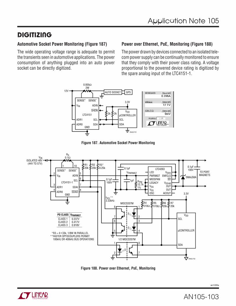
Application Note 105
AN105-103
an105fa
Figure 187. Automotive Socket Power Monitoring
Figure 188. Power over Ethernet, PoE, Monitoring
Automotive Socket Power Monitoring (Figure 187)
The wide operating voltage range is adequate to permit the transients seen in automotive applications. The power consumption of anything plugged into an auto power socket can be directly digitized.
Power over Ethernet, PoE, Monitoring (Figure 188)
The power drawn by devices connected to an isolated tele-com power supply can be continually monitored to ensure that they comply with their power class rating. A voltage proportional to the powered device rating is digitized by the spare analog input of the LTC4151-1.
SENSE+
ADIN
12V
VIN
SHDN
SDA
SCL
ADR0
ADR1
2k 2k
GND
LTC4151
SENSE–
AUTO SOCKET GPS
SCL
SDA
µCONTROLLERVDD
3.3V
0.005Ω2W
DN452 F01
SENSE+
ADIN2
1 10
5
6
3
4
VINISOLATED 48V(44V TO 57V)
VIN
VDD5ENFCLS
SDVDD48
OUTOUT
ACOUT
LEDPWRMGTMIDSPANLEGACYVSSVSSOSCSDAO
SDAI
SCL
ADR0
*R3 = 4 • 33k, 1/8W IN PARALLEL**FASTER OPTOCOUPLERS PERMIT 100kHz OR 400kHz BUS OPERATIONS
ADR1
R120k
GND
LTC4151-1
SENSE–
7
8
SCL
SDA
µCONTROLLER
VDD
3.3V
RS0.1Ω
DN452 F02
R220k
R3*8.25k
RPM12.7k1%
fSCL**3.33kHz
R4510Ω
R620k
R5510Ω
R720k
1µF
LTC4263
SMAJ58A
0.1µFVPWRMGT
0.1µF100V
0.1µF100V
TO PORTMAGNETS
1
2
8MOCD207M
1/2 MOCD207M
7
8
7
1
2
3
4
6
5
CLASS 1CLASS 2CLASS 3
VPWRMGT
0.237V0.417V0.918V
PD CLASS
DIGITIZING

Application Note 105
AN105-104
an105fa
Monitor Current, Voltage and Temperature (Figure 189)
The LTC2990 is a 4-channel, 14-bit ADC fully configurable through an I2C interface to measure single-ended, differ-ential voltages and determine temperature from internal or external diode sensors. For high side current measure-ments two of the inputs are configured for differential input to measure the voltage across a sense resistor. The maximum differential input voltage is limited to ±300mV. Other channels can measure voltage and temperature for a complete system power monitor.
Figure 189. Monitor Current, Voltage and Temperature
DIGITIZING
VCC V1
LTC2990
TINTERNAL
RSENSE2.5V
5V
GND
SDASCLADR0ADR1
MEASURES: TWO SUPPLY VOLTAGES,SUPPLY CURRENT, INTERNAL ANDREMOTE TEMPERATURES
V3
V4
V2
ILOAD
TREMOTE
2990 TA01a
More Digitizing Circuits Are Shown in Other Chapters:FIGURE TITLE
20 Precision, Wide Dynamic Range High-side Current Sensing93 High Voltage Current and Temperature Monitoring130 Small Motor Protection and Control131 Large Motor Protection and Control148 Complete Single Cell Battery Protection208 Remote Current Sensing with Minimal Wiring210 Crystal/Reference Oven Controller211 Power Intensive Circuit Board Monitoring212 Crystal/Reference Oven Controller

Application Note 105
AN105-105
an105fa
This chapter collects a variety of techniques useful in generating controlled levels of current in circuits.
800mA/1A White LED Current Regulator (Figure 190)
The LT6100 is configured for a gain of either 40V/V or 50V/V depending on whether the switch between A2 and VEE is closed or not. When the switch is open (LT6100 gain of 40V/V), 1A is delivered to the LED. When the switch is closed (LT6100 gain of 50V/V), 800mA is delivered. The LT3436 is a boost switching regulator which governs the voltage/current supplied to the LED. The switch “LED ON” connected to the SHDN pin allows for external control of the ON/OFF state of the LED.
Figure 190. 800mA/1A White LED Current Regulator
Bidirectional Current Source (Figure 191)
The LT1990 is a differential amplifier with integrated preci-sion resistors. The circuit shown is the classic Howland current source, implemented by simply adding a sense resistor.
VIN
D1: DIODES INC.D2: LUMILEDS LXML-PW09 WHITE EMITTERL1: SUMIDA CDRH6D28-3R0
0.1µF
22µF16VCER1210
4.99k
6100 TA02
124k
8.2kMMBT2222
LT3436
D1B130
L13µH
SHDN
VSW
FB
GNDLEDON
VIN3.3V TO 4.2V
SINGLE Li-Ion
4.7µF6.3VCER
VC
VS+0.030Ω
D2LED WARNING! VERY BRIGHT
DO NOT OBSERVE DIRECTLYLED
CURRENT
VOUT
VEE A4
LT6100
OPEN: 1ACLOSED: 800mA
A2
VS–
VCC
+ –
Figure 191. Bidirectional Current Source
–
+3
2
6
7
41
+V
–V
LT1990
ILOAD
ILOAD = VCTL/RSENSE ≤ 5mAEXAMPLE: FOR RSENSE =100Ω,
OUTPUT IS 1mA PER 100mV INPUT
VCTL
RSENSE
1990 AI03
REF
CURRENT CONTROL
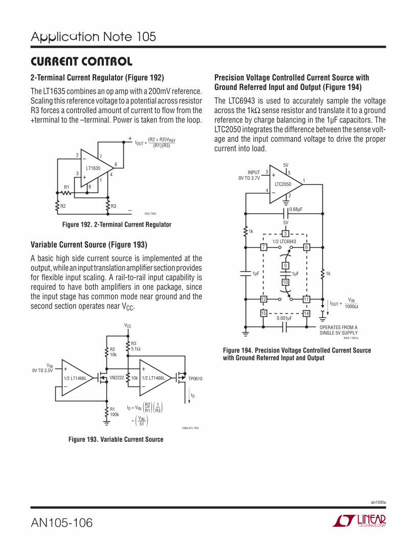
Application Note 105
AN105-106
an105fa
2-Terminal Current Regulator (Figure 192)
The LT1635 combines an op amp with a 200mV reference. Scaling this reference voltage to a potential across resistor R3 forces a controlled amount of current to flow from the +terminal to the –terminal. Power is taken from the loop.
Figure 192. 2-Terminal Current Regulator
Figure 194. Precision Voltage Controlled Current Source with Ground Referred Input and Output
Figure 193. Variable Current Source
Variable Current Source (Figure 193)
A basic high side current source is implemented at the output, while an input translation amplifier section provides for flexible input scaling. A rail-to-rail input capability is required to have both amplifiers in one package, since the input stage has common mode near ground and the second section operates near VCC.
8
3
1635 TA05
2
14
7
6
+
–
R1
R2
–
+LT1635
(R2 + R3)VREF(R1)(R3)
IOUT =
R3
–
+
–
+1/2 LT1466L 1/2 LT1466LVN2222 10k
R1100k
R210k
R35.1Ω
VCC
TP0610
VIN0V TO 2.5V
IO
IO = VIN R2R1( ) 1
R3( )= VIN
51( )1466L/67L TA01
Precision Voltage Controlled Current Source with Ground Referred Input and Output (Figure 194)
The LTC6943 is used to accurately sample the voltage across the 1kΩ sense resistor and translate it to a ground reference by charge balancing in the 1µF capacitors. The LTC2050 integrates the difference between the sense volt-age and the input command voltage to drive the proper current into load.
6943 • TA01a
1µF
0.68µF
1k
1k1µF
1/2 LTC69436
11
15
5
4
3
2
1
–
+LTC2050
3
12
140.001µF
10
9
7
5V
5VINPUT
0V TO 3.7V
IOUT = VIN
1000Ω
OPERATES FROM A SINGLE 5V SUPPLY
CURRENT CONTROL

Application Note 105
AN105-107
an105fa
Precision Voltage Controlled Current Source (Figure 195)
The ultra-precise LTC2053 instrumentation amplifier is configured to servo the voltage drop on sense resistor R to match the command VC. The LTC2053 output capability limits this basic configuration to low current applications.
Boosted Bidirectional Controlled Current Source (Figure 197)
This is a classical Howland bidirectional current source implemented with an LT1990 integrated difference amplifier. The op amp circuit servos to match the RSENSE voltage drop to the input command VCTL. When the load current exceeds about 0.7mA in either direction, one of the boost transistors will start conducting to provide the additional commanded current.
CURRENT CONTROL
VOUT
VC
2053 TA02
14
56
7
5V
8
3
2
0.1µF
0.1µF
2.7k
10k
R
i
LOAD VCR
i = — , i ≤ 5mA
0 < VOUT < (5V – VC)
–
+LTC2053
REFEN
RG
Figure 195. Precision Voltage Controlled Current Source
Figure 197. Boosted Bidirectional Controlled Current Source
Figure 198. 0A to 2A Current Source
Figure 196. Switchable Precision Current Source
Switchable Precision Current Source (Figure 196)
This is a simple current-source configuration where the op amp servos to establish a match between the drop on the sense resistor and that of the 1.2V reference. This particular op amp includes a shutdown feature so the current source function can be switched off with a logic command. The 2kΩ pull-up resistor assures the output MOSFET is off when the op amp is in shutdown mode.
SHDN
IOUT
LT1004-1.24.7µF
2k
*OPTIONAL FOR LOW OUTPUT CURRENTS, R* = R
R
4V TO 44V
TP0610
1637 TA01
R*
–
+LT1637
IOUT =
e.g., 10mA = 120Ω
1.2R
+
–
+3
2
6
7
41
+V
–V
LT1990
ILOAD
ILOAD = VCTL/RSENSE 100mAEXAMPLE: FOR RSENSE =10Ω,
OUTPUT IS 1mA PER 10mV INPUT
VCTL
RSENSE
1990 AI04
10µF
1k
1k
REF
CZT751
CZT651
+
0A to 2A Current Source (Figure 198)
The LT1995 amplifies the sense resistor drop by 5V/V and subtracts that from VIN, providing an error signal to an LT1880 integrator. The integrated error drives the P-MOSFET as required to deliver the commanded current.
RS0.2Ω
10nF
LT1995G = 5
–15V
–15V
15V 10nF
15V
IOUT
VIN
1k
1995 TA04
100Ω
–
+LT1880
REF
IRF9530
M4M1
P1P4
IOUT =VIN
5 • RS

Application Note 105
AN105-108
an105fa
CURRENT CONTROL
Figure 199. Fast Differential Current Source
Figure 200. 1A Voltage-Controlled Current Sink
Figure 201. Voltage Controlled Current Source
Fast Differential Current Source (Figure 199)
This is a variation on the Howland configuration, where load current actually passes through a feedback resistor as an implicit sense resistance. Since the effective sense resistance is relatively large, this topology is appropriate for producing small controlled currents.
LT1022 • TA07
6
10pF15V
–15V
3
2 7
4
LT1022
+
–VIN1
RLIOUT
IOUT =VIN2 – VIN1
VIN2
R* R*
R*
R*
R
2IOUTP-P • RL
*MATCH TO 0.01% FULL-SCALE POWER BANDWIDTH = 1MHz FOR IOUTR = 8VP-P = 400kHz FOR IOUTR = 20VP-P MAXIMUM IOUT = 10mAP-P COMMON MODE VOLTAGE AT LT1022 INPUT =
1A Voltage-Controlled Current Sink (Figure 200)
This is a simple controlled current sink, where the op amp drives the N-MOSFET gate to develop a match between the 1Ω sense resistor drop and the VIN current command. Since the common mode voltage seen by the op amp is near ground potential, a “single supply” or rail-to-rail type is required in this application.
–
+VIN
V+
1/2LT1492
RL
IOUT
1492/93 TA06
1k
100Ω
100pF
Si9410DYN-CHANNEL
1Ω
V+
IOUT = VIN1Ω
tr < 1µs
Voltage Controlled Current Source (Figure 201)
Adding a current sense amplifier in the feedback loop of an adjustable low dropout voltage regulator creates a simple voltage controlled current source. The range of output current sourced by the circuit is set only by the current capability of the voltage regulator. The current sense amplifier senses the output current and feeds back a current to the summing junction of the regulator’s error amplifier. The regulator will then source whatever current is necessary to maintain the internal reference voltage at the summing junction. For the circuit shown a 0V to 5V control input produces 500mA to 0mA of output current.
–
+
–
+
RS1Ω
RLOAD
VIN
LTC6101
LT3021
1k0.2VREF
24k
2.5k
V+
5V
10µF
FOR VIN = 0V TO 5V, IOUT = 500mA TO 0mA
IOUT = 100mA/V
+IN

Application Note 105
AN105-109
an105fa
CURRENT CONTROLAdjustable High Side Current Source (Figure 202)
The wide-compliance current source shown takes advan-tage of the LT1366’s ability to measure small signals near the positive supply rail. The LT1366 adjusts Q1’s gate volt-age to force the voltage across the sense resistor (RSENSE) to equal the voltage between VDC and the potentiometer’s wiper. A rail-to-rail op amp is needed because the voltage across the sense resistor is nearly the same as VDC. Q2 acts as a constant current sink to minimize error in the reference voltage when the supply voltage varies. At low input voltage, circuit operation is limited by the Q1 gate drive requirement. At high input voltage, circuit operation is limited by the LT1366’s absolute maximum ratings.
–
+1/2 LT1366
1k
RSENSE0.2Ω
40k
Q1MTP23P06
ILOAD
5V < VCC < 30V0A < ILOAD < 1A AT VCC = 5V0mA < ILOAD < 160mA AT VCC = 30V
Q22N4340
VCC
100Ω
0.0033µFLT1004-1.2
RP10k
LT1366 F07
Figure 202. Adjustable High Side Current Source
Programmable Constant Current Source (Figure 203)
The current output can be controlled by a variable resistor (RPROG) connected from the PROG pin to ground on the LT1620. The LT1121 is a low dropout regulator that keeps the voltage constant for the LT1620. Applying a shutdown command to the LT1121 powers down the LT1620 and eliminates the base drive to the current regulation pass transistor, thereby turning off IOUT.
Snap Back Current Limiting (Figure 204)
The LT1970 provides current detection and limiting features built-in. In this circuit, the logic flags that are produced in a current limiting event are connected in a feedback ar-rangement that in turn reduces the current limit command to a lower level. When the load condition permits the cur-rent to drop below the limiting level, then the flags clear and full current drive capability is restored automatically.

Application Note 105
AN105-110
an105fa
CURRENT CONTROL
Figure 203. Programmable Constant Current Source
Figure 204. Snap Back Current Limiting
AVG
PROG
VCC
+IN
SENSE
LT1620MS8
1
2
3
4
8
7IOUT
GND
–IN
6
5
0.1µF10k1%
RPROG
18k 0.1µF1µF
IPROG2N3904
22Ω
VN2222LM
OUTIN
GNDSHDN
SHUTDOWN
0.1µF
6VTO 28V
470Ω
0.1Ω
LT1121CS8-5
0.1µF
IOUT 0A TO 1A
IOUT = (IPROG)(10,000)RPROG = 40k FOR 1A OUTPUT
LT1620/21 • TA01
8 1
5 3
D45VH10
+
VCSRC
COMMONVEE
VCSNK
V–FILTER
V+
12V
ENVCC
ISNKISRC
SENSE–SENSE+
TSDOUT
+INVIN
LT1970
–12V
–IN
RS1Ω
RL
1970 F04
RG10k
RF10k
R32.55k
R239.2k
R154.9k
IMAX500mA
–500mA
50mA0IOUT
ILOW
VCC • R2(R1 + R2) • 10 • RS
IMAX
VCC • (R2||R3)[R1 + (R2||R3)] • 10 • RS
ILOW
More Current Control Circuits Are Shown in Other Chapters:FIGURE TITLE
120 Bidirectional Current Sensing in H-Bridge Drivers129 Simple DC Motor Torque Control170 Use Comparator Output to Initialize Interrupt Routines

Application Note 105
AN105-111
an105fa
Offset voltage and bias current are the primary sources of error in current sensing applications. To maintain precision operation the use of zero drift amplifier virtually eliminates the offset error terms.
Precision High Side Power Supply Current Sense (Figure 205)
This is a low voltage, ultra high precision monitor featuring a zero drift instrumentation amplifier (IA) that provides rail-to-rail inputs and outputs. Voltage gain is set by the feedback resistors. Accuracy of this circuit is set by the quality of resistors selected by the user, small-signal range is limited by VOL in single-supply operation. The voltage rating of this part restricts this solution to applications of <5.5V. This IA is sampled, so the output is discontinuous with input changes, thus only suited to very low frequency measurements.
PRECISION
–
+LTC6800
45
6
7OUT100mV/AOF LOADCURRENT10k
1.5mΩ
0.1µF
150Ω
6800 TA01
ILOAD
82
VREGULATOR
3
LOAD
Figure 205. Precision High Side Power Supply Current Sense
Figure 206. High Side Power Supply Current Sense
Figure 207. Second Input R Minimizes Error Due to Input Bias Current
High Side Power Supply Current Sense (Figure 206)
The low offset error of the LTC6800 allows for unusually low sense resistance while retaining accuracy.
Second Input R Minimizes Error Due to Input Bias Current (Figure 207)
The second input resistor decreases input error due caused by the input bias current. For smaller values of RIN this may not be a significant consideration.
–
+LTC6800
45
6
7OUT100mV/AOF LOADCURRENT10k
1.5mΩ
0.1µF
150Ω
6800 TA01
ILOAD
82
VREGULATOR
3
LOAD
LTC6101ROUT
VOUT
6101 F04
RIN–
V+
LOAD
RSENSERIN
+
–+
RIN+ = RIN
– – RSENSE
V+V–
OUT
–IN+IN

Application Note 105
AN105-112
an105fa
PRECISIONRemote Current Sensing with Minimal Wiring (Figure 208)
Since the LTC6102 (and others) has a current output that is ordinarily converted back to a voltage with a local load resistance, additional wire resistance and ground offsets don’t directly affect the part behavior. Consequently, if the load resistance is placed at the far end of a wire, the voltage developed at the destination will be correct with respect to the destination ground potential.
Use Kelvin Connections to Maintain High Current Accuracy (Figure 209)
Significant errors are caused by high currents flowing through PCB traces in series with the connections to the sense amplifier. Using a sense resistor with integrated VIN sense terminals provides the sense amplifier with only the voltage across the sense resistor. Using the LTC6104 maintains precision for currents flowing in both directions, ideal for battery charging applications.
Figure 208. Remote Current Sensing with Minimal Wiring
Figure 209. Use Kelvin Connections to Maintain High Current Accuracy
LTC61026102 TA09
RIN–
V+
LOAD
RSENSE
–+
V+
–INF
V–
OUTLONG WIRE
VREG0.1µF
TIE AS CLOSE TO RIN AS POSSIBLE
–INS+IN
ROUT
ADC
fC = 12 • π • ROUT • COUT
REMOTE ADC
COUT
+ –
8 7 6
4
+INA
OUT
+
–
VSVS
A
LTC6104
–INA –INB
RINRIN
TOCHARGER/LOAD
RSENSE
VSENSE +–
+INB
V–
ILOAD
+
CURRENTMIRROR
+–
5
B
ROUT
VREF
6104 F02
VOUT+–
1

Application Note 105
AN105-113
an105fa
Crystal/Reference Oven Controller (Figure 210)
High precision instrumentation often use small ovens to establish constant operation temperature for critical oscilla-tors and reference voltages. Monitoring the power (current and voltage) to the heater as well as the temperature is required in a closed-loop control system.
Power Intensive Circuit Board Monitoring (Figure 211)
Many systems contain densely populated circuit boards using high power dissipation devices such as FPGAs. 8-channel, 14-bit ADC LTC2991 can be used to moni-tor device power consumption with voltage and current measurements as well as temperatures at several points on the board and even inside devices which provide die temp monitoring. A PWM circuit is also built-in to provide closed-loop control of PCB operating temperature.
VCC V1
LTC2990
HEATERPWR = I •V0.1Ω
HEATERVOLTAGE
2-WIREI2C
INTERFACE
5V
GND
470pF
FEEDFORWARD
FEEDBACK
HEATER
HEATER CONSTRUCTION:5FT COIL OF #34 ENAMEL WIRE~1.6Ω AT 70°CPHEATER = ~0.4W WITH TA = 20°C
HEATER POWER = α • (TSET – TAMB) + β • ∫(TOVEN – TSET) dt
20°CAMBIENT
STYROFOAMINSULATION
70°COVEN
TOVEN
α = 0.004W, β = 0.00005W/DEG-s
MMBT3904SDASCLADR0ADR1
V3
V4
V2
2990 TA10TINTERNAL
CURRENT AND TEMPERATURE CONFIGURATION:CONTROL REGISTER: 0x59TAMB REG 4, 5 0.0625°C/LSBIHEATER REG 6, 7 269µVLSBTHEATER REG A, B 0.0625°C/LSBVCC REG E, F 2.5V + 305.18µV/LSB
VOLTAGE AND TEMPERATURE CONFIGURATION:CONTROL REGISTER: 0x58TAMB REG 4, 5 0.0625°C/LSBV1, V2 REG 8, 9 305.18µVLSBTOVEN REG A, B 0.0625°C/LSBVCC REG E, F 2.5V + 305.18µV/LSB
0.1µF
VCC
2-WIREI2C INTERFACE
V1
LTC2991
TAMBIENT
RSENSE
3.3V
5V
1.2V
2.5V
GND
SDA
SCL
ADR0
ADR1
ADR2
3.3V I/O
2.5V I/O
1.2V CORE
FPGA
FPGATEMPERATURE
BOARDTEMPERATURE
V3 V4
V5
V6
V7
V8
PWM TO FAN
V2
2991 TA01a
Figure 210. Crystal/Reference Oven Controller
Figure 211. Power Intensive Circuit Board Monitoring
PRECISION

Application Note 105
AN105-114
an105fa
PRECISION
VCC
2-WIREI2C INTERFACE
V1
LTC2991
TAMBIENT
5V
GND
SDA
SCL
ADR0
ADR1
ADR2
V3
V4
V5
V6
OTHER APPLICATIONS
VOLTAGE AND CURRENT (POWER) MONITOR
OVENTSET 70°C
TEMPERATURESENSOR
HEATER
VCC
V7
V8
PWM
V2
2991 TA11
–
+100k
1µF
LT6240
100k
1M
VCC
5V
VOLTAGE, CURRENT, TEMPERATURE AND PWM CONFIGURATION:CONTROL REGISTER 0x06: 0x01
TAMBIENT REG 1A, 1B 0.0625°C/LSBVHEATER REG 0A, 0B 305µV/LSBIHEATER REG 0C, 0D 19.4µV/RHEATERA/LSBTOVEN REG 16, 17 0.0625°C/LSBVCC REG 1C, 1D 2.5V + 305.18µV/LSB
0x07: 0xA0PWM, TINTERNAL, VCC REG: PWM REGISTER
0x08: 0x500x09: 0x1B
Crystal/Reference Oven Controller (Figure 212)
High precision instrumentation often use small ovens to establish constant operation temperature for critical oscilla-tors and reference voltages. Monitoring the power (current
Figure 212. Crystal/Reference Oven Controller
and voltage) to the heater as well as the temperature is required in a closed-loop control system. The LTC2991 includes a PWM output which can provide closed-loop control of the heater.

Application Note 105
AN105-115
an105fa
PRECISIONMore Precision Circuits Are Shown in Other Chapters:
FIGURE TITLE20 Precision, Wide Dynamic Range High-side Current Sensing21 Sensed Current Includes Monitor Circuit Supply Current58 Bidirectional Precision Current Sensing93 High Voltage Current and Temperature Monitoring124 Monitor H-Bridge Motor Current Directly128 Fixed Gain DC Motor Current Monitor136 Coulomb Counting Battery Gas Gauge145 High Voltage Battery Coulomb Counting146 Low Voltage Battery Coulomb Counting147 Single Cell Lithium-Ion Battery Coulomb Counter176 Directly Digitize Current with 16-Bit Resolution179 Digitizing Charging and Loading Current in a Battery Monitor182 Power Sensing with Built In A to D Converter183 Isolated Power Measurement184 Fast Data Rate Isolated Power Measurement185 Adding Temperature Measurement to Supply Power Measurement186 Current, Voltage and Fuse Monitoring189 Monitor Current, Voltage and Temperature

Application Note 105
AN105-116
an105fa
To measure current over a wide range of values requires gain changing in the current sense amplifier. This allows the use of a single value of sense resistor. The alternative approach is to switch values of sense resistor. Both ap-proaches are viable for wide range current sensing.
Dual LTC6101’s Allow High-Low Current Ranging (Figure 213)
Using two current sense amplifiers with two values of sense resistors is an easy method of sensing current over a wide range. In this circuit the sensitivity and resolution of measurement is 10 times greater with low currents, less than 1.2A, than with higher currents. A comparator detects higher current flow, up to 10A, and switches sensing over to the high current circuitry.
Adjust Gain Dynamically for Enhanced Range (Figure 214)
Instead of having fixed gains of 10, 12.5, 20, 25, 40, and 50, this circuit allows selecting between two gain settings. An N-MOSFET switch is placed between the two gain-setting
WIDE RANGE
6101 F03b
–+ –+
–+
R57.5k
VIN
301301
VOUT
ILOAD
5
1
3
LTC6101
2
4
RSENSE LO100m
M1Si4465
10k
CMPZ4697
7.5k
VIN
1.74M4.7k
Q1CMPT5551
40.2k
3
4
5
6
12
8
7
619k
HIGHRANGE
INDICATOR(ILOAD > 1.2A)
VLOGIC(3.3V TO 5V)
LOW CURRENT RANGE OUT2.5V/A
(VLOGIC +5V) ≤ VIN ≤ 60V
0 ≤ ILOAD ≤ 10A
HIGH CURRENT RANGE OUT250mV/A
301 301
5
1
3
LTC6101
2
4
RSENSE HI10m
VLOGIC
BAT54C
LTC1540
terminals (A2, A4) and ground to provide selection of gain = 10 or gain = 50, depending on the state of the gate drive. This provides a wider current measurement range than otherwise possible with just a single sense resistor.
VOUT
FIL
VCC
0V(GAIN = 10)
5V(GAIN = 50)
6100 TA05
RSENSE
LT6100 VS– VS
+
VEE
2N7002
A2 A4
TO LOAD
5V
ISENSE
FROM SOURCE
– +
Figure 213. Dual LTC6101’s Allow High-Low Current Ranging
Figure 214. Adjust Gain Dynamically for Enhanced Range
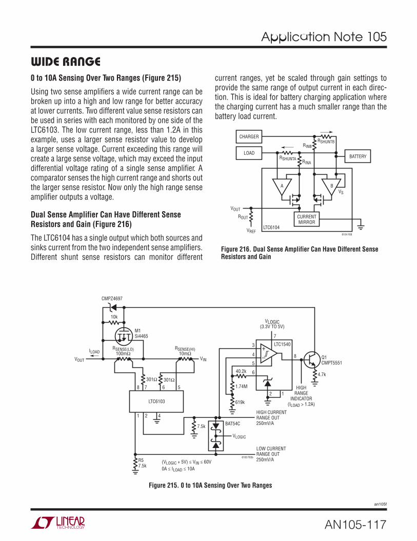
Application Note 105
AN105-117
an105f
WIDE RANGE
Figure 215. 0 to 10A Sensing Over Two Ranges
Figure 216. Dual Sense Amplifier Can Have Different Sense Resistors and Gain
0 to 10A Sensing Over Two Ranges (Figure 215)
Using two sense amplifiers a wide current range can be broken up into a high and low range for better accuracy at lower currents. Two different value sense resistors can be used in series with each monitored by one side of the LTC6103. The low current range, less than 1.2A in this example, uses a larger sense resistor value to develop a larger sense voltage. Current exceeding this range will create a large sense voltage, which may exceed the input differential voltage rating of a single sense amplifier. A comparator senses the high current range and shorts out the larger sense resistor. Now only the high range sense amplifier outputs a voltage.
Dual Sense Amplifier Can Have Different Sense Resistors and Gain (Figure 216)
The LTC6104 has a single output which both sources and sinks current from the two independent sense amplifiers. Different shunt sense resistors can monitor different
current ranges, yet be scaled through gain settings to provide the same range of output current in each direc-tion. This is ideal for battery charging application where the charging current has a much smaller range than the battery load current.
6103 F03b
301Ω
3
4
5
6
2 1
8
7
VOUT VIN
RSENSE(LO)100mΩ
M1Si4465
R57.5k
ILOAD
10k
CMPZ4697
301Ω
8 7 6 5
421
1.74M
4.7k
Q1CMPT5551
619k
40.2k
LTC1540
VLOGIC(3.3V TO 5V)
7.5k
VLOGIC
BAT54C
HIGH CURRENTRANGE OUT250mV/A
HIGHRANGE
INDICATOR(ILOAD > 1.2A)
LOW CURRENTRANGE OUT250mV/A
RSENSE(HI)10mΩ
+–
(VLOGIC + 5V) ≤ VIN ≤ 60V0A ≤ ILOAD ≤ 10A
LTC6103
VOUT
ROUT
VS
A
LTC6104
RINB
RINARSHUNTA
CURRENTMIRROR
LOADBATTERY
B
6104 F08VREF
RSHUNTBCHARGER

Application Note 105
AN105-118
an105fa
WIDE RANGEMore Wide Range Circuits Are Shown in Other Chapters:
FIGURE TITLE20 Precision, Wide Dynamic Range High-side Current Sensing58 Bidirectional Precision Current Sensing208 Remote Current Sensing with Minimal Wiring
Linear Technology Corporation1630 McCarthy Blvd., Milpitas, CA 95035-7417 (408) 432-1900 FAX: (408) 434-0507 www.linear.com LINEAR TECHNOLOGY CORPORATION 2005
LT 0614 REV A • PRINTED IN USA