AN ACTIVE POWER SUPPLY FILTER WITH ULTRA WIDE …
54
AN ACTIVE POWER SUPPLY FILTER WITH ULTRA WIDE BANDWIDTH A Thesis Submitted to the Graduate Faculty of the North Dakota State University of Agriculture and Applied Science By Brian James Booth In Partial Fulfillment of the Requirements for the Degree of MASTER OF SCIENCE Major Department: Electrical and Computer Engineering May 2016 Fargo, North Dakota
Transcript of AN ACTIVE POWER SUPPLY FILTER WITH ULTRA WIDE …

AN ACTIVE POWER SUPPLY FILTER WITH ULTRA WIDE BANDWIDTH
A ThesisSubmitted to the Graduate Faculty
of theNorth Dakota State University
of Agriculture and Applied Science
By
Brian James Booth
In Partial Fulfillment of the Requirementsfor the Degree of
MASTER OF SCIENCE
Major Department:Electrical and Computer Engineering
May 2016
Fargo, North Dakota
NORTH DAKOTA STATE UNIVERSITY
Graduate School
Title
AN ACTIVE POWER SUPPLY FILTER WITH ULTRA WIDE BANDWIDTH
By
Brian James Booth
The supervisory committee certifies that this thesis complies with North Dakota State University’s
regulations and meets the accepted standards for the degree of
MASTER OF SCIENCE
SUPERVISORY COMMITTEE:
Dr. Benjamin D. Braaten
Chair
Dr. Ivan T. Lima, Jr.
Dr. Debasis Dawn
Dr. Davis Cope
Approved:
July 6th, 2016
Date
Dr. Scott SmithDepartment Chair

ABSTRACT
An active transformerless common mode filter is designed for use with switching mode power
supplies with a switching frequency greater than 1MHz. The filter utilizes an amplifier in a voltage
sensing current adjusting architecture to cancel out common mode noise generated by the switching
power supply. The filter is analyzed using a transfer function, simulation, and measurements.
Several possible feedback configurations are examined and benefits of different configurations are
explained. The active filter is shown to have superior performance to only passive components at
frequencies up to 20MHz. Spectral domain, time domain, and S21 measurements are given to show
the filter’s effectiveness.
iii

ACKNOWLEDGEMENTS
I would like to thank my advisor, Dr. Braaten, for his support and patience as I worked to
complete my thesis. His guidance and suggestions were always appreciated.
I would like to thank my committee Dr. Davis Cope, Dr. Debasis Dawn, and Dr. Ivan
Lima. They have all taught me many things in their courses. I appreciate their support and
suggestions on my thesis work.
I would like to thank John Deere for sponsoring my Master’s Degree. Specifically I would
like to thank my coworkers for their encouragement and reminders to get my thesis work done.
I would like to thank my wife Kimi for helping me complete my thesis, even when it seemed
like it would never get done. She truly has been my encouraging advocate throughout this whole
process.
iv

DEDICATION
To my wonderful wife Kimi and my daughter Rozalyn.
v

TABLE OF CONTENTS
ABSTRACT . . . . . . . . . . . . . . . . . . . . . . . . . . . . . . . . . . . . . . . . . . . . . iii
ACKNOWLEDGEMENTS . . . . . . . . . . . . . . . . . . . . . . . . . . . . . . . . . . . . . iv
DEDICATION . . . . . . . . . . . . . . . . . . . . . . . . . . . . . . . . . . . . . . . . . . . . v
LIST OF FIGURES . . . . . . . . . . . . . . . . . . . . . . . . . . . . . . . . . . . . . . . . . viii
CHAPTER 1. INTRODUCTION . . . . . . . . . . . . . . . . . . . . . . . . . . . . . . . . . 1
CHAPTER 2. THEORY AND DESIGN . . . . . . . . . . . . . . . . . . . . . . . . . . . . . 2
2.1. Introduction . . . . . . . . . . . . . . . . . . . . . . . . . . . . . . . . . . . . . . . . . 2
2.2. Conducted and Radiated Emissions . . . . . . . . . . . . . . . . . . . . . . . . . . . . 2
2.3. Switched-Mode Power Supplies . . . . . . . . . . . . . . . . . . . . . . . . . . . . . . 4
2.3.1. Switched-Mode Power Supplies as a source of EMI . . . . . . . . . . . . . . . 4
2.3.2. Equivalent Common Mode Noise Source Model . . . . . . . . . . . . . . . . . 6
2.4. Filtering . . . . . . . . . . . . . . . . . . . . . . . . . . . . . . . . . . . . . . . . . . . 8
2.4.1. Definition of S21 . . . . . . . . . . . . . . . . . . . . . . . . . . . . . . . . . . 8
2.4.2. Traditional Filtering . . . . . . . . . . . . . . . . . . . . . . . . . . . . . . . . 9
2.4.3. Active Filtering . . . . . . . . . . . . . . . . . . . . . . . . . . . . . . . . . . . 9
2.4.4. Voltage Sensing Current Adjusting Architecture . . . . . . . . . . . . . . . . 12
CHAPTER 3. RESULTS . . . . . . . . . . . . . . . . . . . . . . . . . . . . . . . . . . . . . . 14
3.1. Introduction . . . . . . . . . . . . . . . . . . . . . . . . . . . . . . . . . . . . . . . . . 14
3.2. Analysis of Proposed Active Filter . . . . . . . . . . . . . . . . . . . . . . . . . . . . 14
3.2.1. Transfer Function . . . . . . . . . . . . . . . . . . . . . . . . . . . . . . . . . 14
3.2.2. Determination of Zfeedback . . . . . . . . . . . . . . . . . . . . . . . . . . . . . 14
3.2.3. Ideal Simulation . . . . . . . . . . . . . . . . . . . . . . . . . . . . . . . . . . 17
3.2.4. Bandwidth Limited Simulation . . . . . . . . . . . . . . . . . . . . . . . . . . 17
3.3. Filter Synthesis . . . . . . . . . . . . . . . . . . . . . . . . . . . . . . . . . . . . . . . 19
vi
3.4. Measurements . . . . . . . . . . . . . . . . . . . . . . . . . . . . . . . . . . . . . . . . 25
3.4.1. S21 Measurment . . . . . . . . . . . . . . . . . . . . . . . . . . . . . . . . . . 25
3.4.2. Frequency Domain . . . . . . . . . . . . . . . . . . . . . . . . . . . . . . . . . 33
3.4.3. Time Domain . . . . . . . . . . . . . . . . . . . . . . . . . . . . . . . . . . . . 37
CHAPTER 4. CONCLUSION . . . . . . . . . . . . . . . . . . . . . . . . . . . . . . . . . . . 40
BIBLIOGRAPHY . . . . . . . . . . . . . . . . . . . . . . . . . . . . . . . . . . . . . . . . . . 41
APPENDIX . . . . . . . . . . . . . . . . . . . . . . . . . . . . . . . . . . . . . . . . . . . . . . 43
vii
LIST OF FIGURES
Figure Page
2.1. LISN as defined in CISPR 25 . . . . . . . . . . . . . . . . . . . . . . . . . . . . . . . . . 3
2.2. Radiated Emissions Test Setup . . . . . . . . . . . . . . . . . . . . . . . . . . . . . . . . 3
2.3. CISPR 25 LISN Impedance from port B to P . . . . . . . . . . . . . . . . . . . . . . . . 4
2.4. DC to DC Buck Switched-Mode Power Supply . . . . . . . . . . . . . . . . . . . . . . . 5
2.5. Switch Node Voltage for Switched-Mode Power Supply . . . . . . . . . . . . . . . . . . . 5
2.6. Heat Sink Cross Section . . . . . . . . . . . . . . . . . . . . . . . . . . . . . . . . . . . . 6
2.7. DC to DC Buck Switched-Mode Power Supply with Parasitic Heat Sink Capacitance . . 7
2.8. CISPR 25 Setup with DC to DC Buck Switched-Mode Power Supply . . . . . . . . . . . 7
2.9. CISPR 25 Setup with an Equivalent Common Mode Noise Source Model . . . . . . . . . 8
2.10. Traditional Power Supply Filter . . . . . . . . . . . . . . . . . . . . . . . . . . . . . . . . 9
2.11. Current Sensing Current Adjusting Schematic . . . . . . . . . . . . . . . . . . . . . . . . 10
2.12. Voltage Sensing Current Adjusting Schematic . . . . . . . . . . . . . . . . . . . . . . . . 10
2.13. Current Sensing Voltage Adjusting Schematic . . . . . . . . . . . . . . . . . . . . . . . . 11
2.14. Voltage Sensing Voltage Adjusting Schematic . . . . . . . . . . . . . . . . . . . . . . . . 11
2.15. Proposed Voltage Sensing Voltage Adjusting Schematic . . . . . . . . . . . . . . . . . . 12
2.16. VSCA Filter in System Application . . . . . . . . . . . . . . . . . . . . . . . . . . . . . 13
3.1. System schematic with proposed VSCA filter for analysis . . . . . . . . . . . . . . . . . 15
3.2. MATLAB plot of voltage across the LISN impedance predicted by 3.1 using three possi-ble feedback configurations, a shorted feedback network, a 100Ω feedback network, anda 1GΩ feedback network. . . . . . . . . . . . . . . . . . . . . . . . . . . . . . . . . . . . 15
3.3. MATLAB plot comparing four 1nF capacitors connected in parallel with ZLISN to pro-posed filter with shorted feedback. . . . . . . . . . . . . . . . . . . . . . . . . . . . . . . 16
3.4. Plot of S21 comparing MATLAB code using 3.1 to Keysight ADS simulation using idealan op-amp and a shorted feedback network. . . . . . . . . . . . . . . . . . . . . . . . . . 17
3.5. Plot of S21 comparing MATLAB code using 3.1 to Keysight ADS simulation using idealan op-amp and a 100Ω feedback network. . . . . . . . . . . . . . . . . . . . . . . . . . . 18
viii

3.6. Plot of S21 comparing MATLAB code using 3.1 with 1GΩ feedback network to KeysightADS simulation using an ideal op-amp with a gain of 10000 and an open feedback network. 19
3.7. Bandwidth limited simulation circuit schematic in Keysight’s ADS 2015. . . . . . . . . . 20
3.8. S21 Bandwidth limited circuit simulation results using three different feedback networkconfigurations: a shorted feedback network, a 100Ω network, and an open feedbacknetwork. The op amp was set to have a bandwidth of 400MHz. . . . . . . . . . . . . . . 20
3.9. Results of S21 bandwidth limited circuit simulation with 100Ω feedback compared toMATLAB predicted results using 3.1 with a 100Ω feedback configuration. . . . . . . . . 21
3.10. Voltage magnitude at output of op amp for both an ideal and bandwidth limited circuitsimulation with 100Ω. . . . . . . . . . . . . . . . . . . . . . . . . . . . . . . . . . . . . . 22
3.11. Voltage phase at output of op amp for both an ideal and bandwidth limited circuitsimulation with 100Ω. . . . . . . . . . . . . . . . . . . . . . . . . . . . . . . . . . . . . . 23
3.12. Circuit simulation with 100Ω feedback and a bandwidth limited op-amp with threedifferent bandwidths, 100MHz, 200MHz, and 400MHz. . . . . . . . . . . . . . . . . . . . 24
3.13. Photo of designed circuit. A quarter is given for size comparison. . . . . . . . . . . . . . 25
3.14. Schematic of synthesized circuit, TI’s THS4271 was used for U1. . . . . . . . . . . . . . 26
3.15. Test Setup for S21 Measurements . . . . . . . . . . . . . . . . . . . . . . . . . . . . . . . 27
3.16. Plot of S21 with a 10dBm source applied to circuits under test with a 50Ω resistor inseries with a 220pF capacitor as source impedance. The test circuit uses three differentpossible feedback networks, a shorted network, an open network, and an open circuitnetwork. The plot compares the active filter to four 1nF capacitors and a setup with nofilter present. . . . . . . . . . . . . . . . . . . . . . . . . . . . . . . . . . . . . . . . . . . 28
3.17. Plot of measured S21 of test circuit with an open feedback configuration compared toMATLAB code using 3.1 with a 1GΩ feedback network. . . . . . . . . . . . . . . . . . . 29
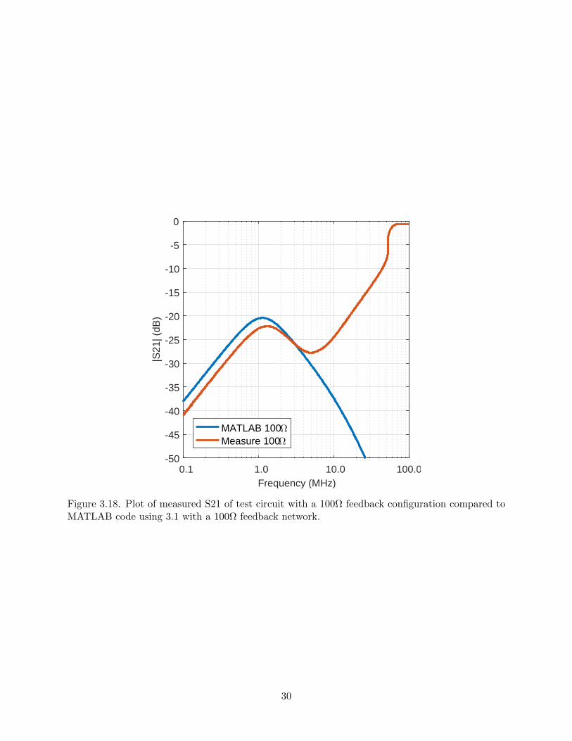
3.18. Plot of measured S21 of test circuit with a 100Ω feedback configuration compared toMATLAB code using 3.1 with a 100Ω feedback network. . . . . . . . . . . . . . . . . . . 30
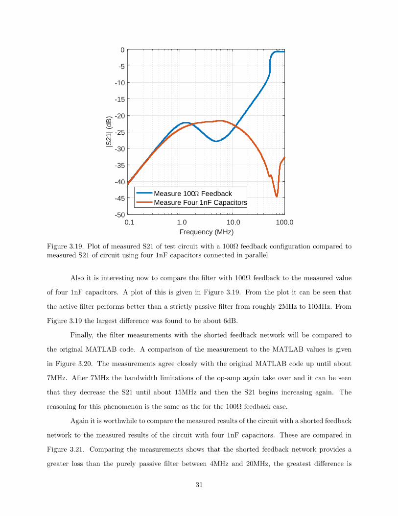
3.19. Plot of measured S21 of test circuit with a 100Ω feedback configuration compared tomeasured S21 of circuit using four 1nF capacitors connected in parallel. . . . . . . . . . 31
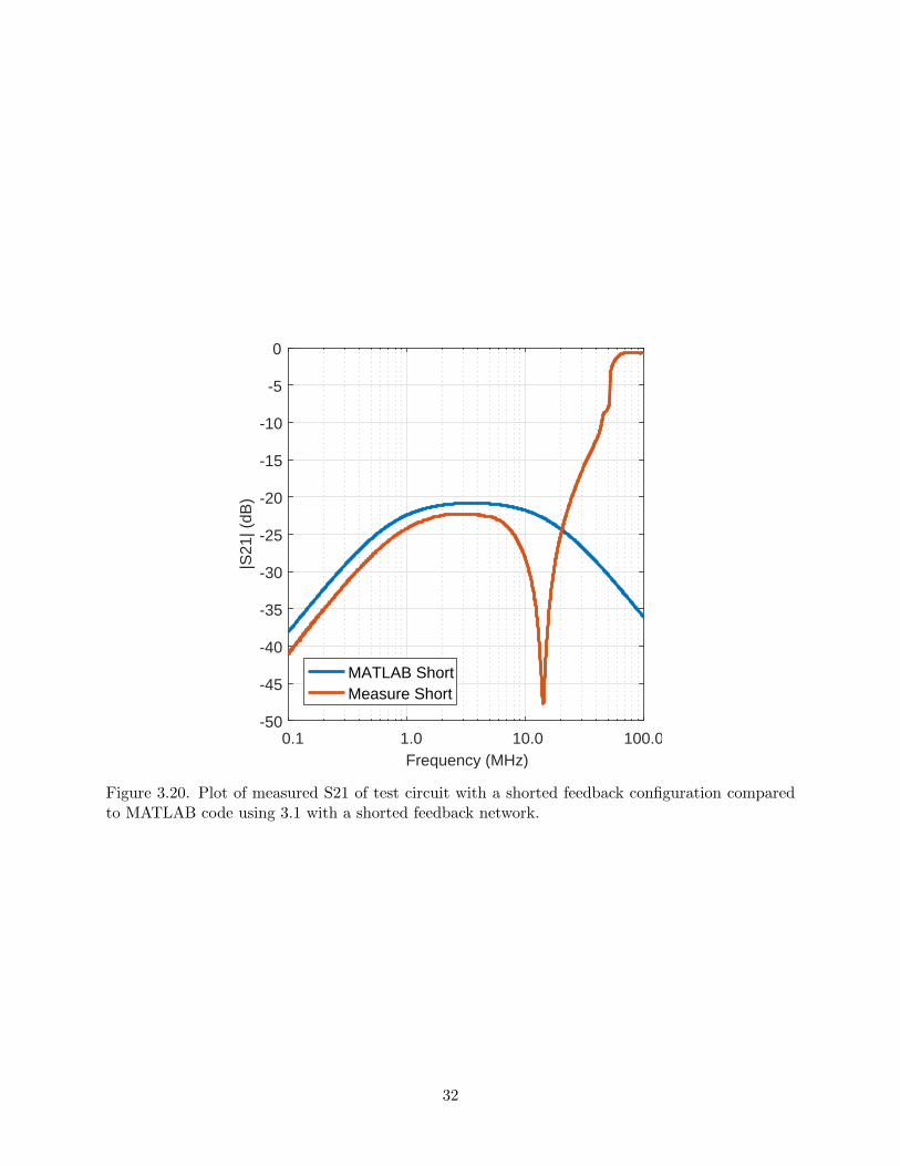
3.20. Plot of measured S21 of test circuit with a shorted feedback configuration compared toMATLAB code using 3.1 with a shorted feedback network. . . . . . . . . . . . . . . . . 32
3.21. Plot of measured S21 of test circuit with a shorted feedback configuration compared tomeasured S21 of circuit using four 1nF capacitors connected in parallel. . . . . . . . . . 33
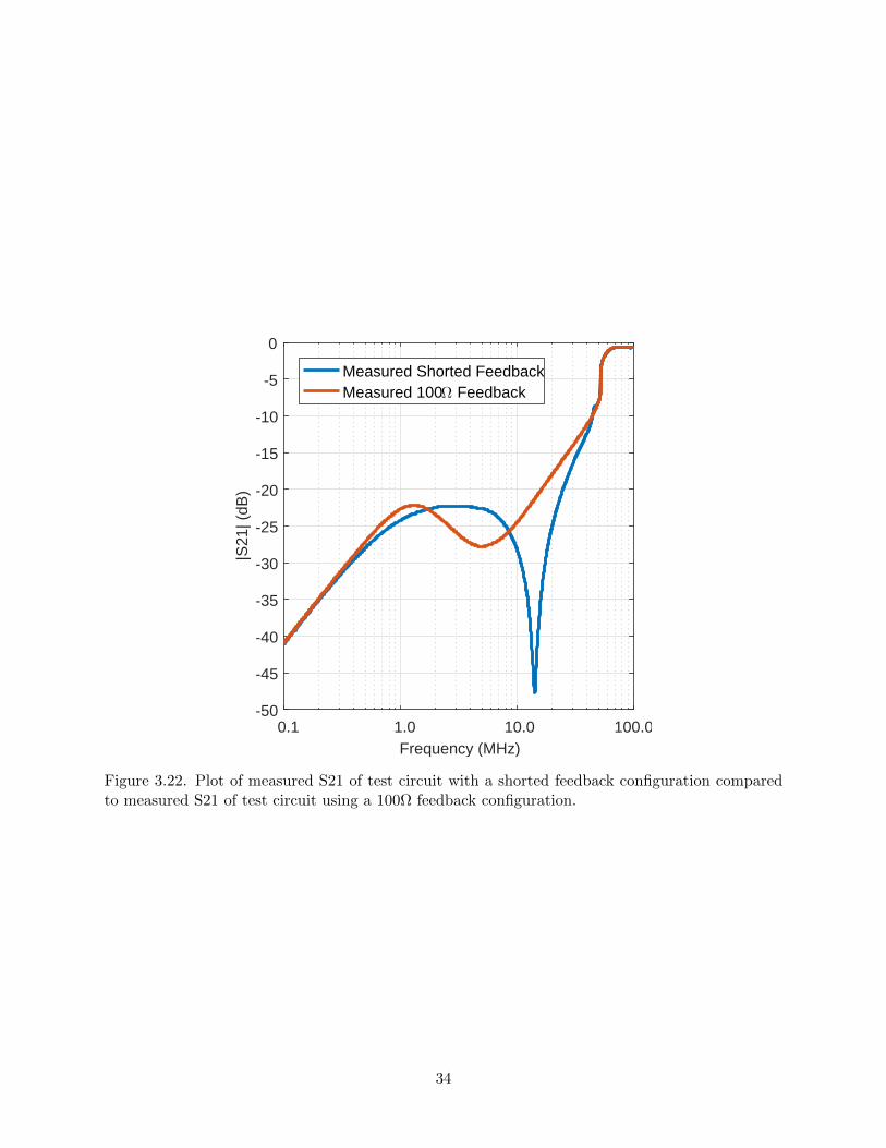
3.22. Plot of measured S21 of test circuit with a shorted feedback configuration compared tomeasured S21 of test circuit using a 100Ω feedback configuration. . . . . . . . . . . . . . 34
ix
3.23. Test setup for time and frequency measurements. . . . . . . . . . . . . . . . . . . . . . 35
3.24. Plot of spectral measurements with a 1MHz square wave applied to circuits under testwith a 50Ω resistor in series with a 220pF capacitor as source impedance. The inputwaveform was 3V peak to peak. The proposed filter circuit was tested with a shortedfeedback configuration, 100Ω feedback configuration, and open feedback configuration.The proposed filter measurements are also compared to four 1nF capacitors in paralleland a test setup without a filter. . . . . . . . . . . . . . . . . . . . . . . . . . . . . . . . 36
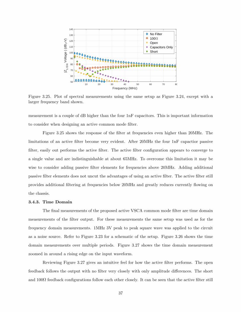
3.25. Plot of spectral measurements using the same setup as Figure 3.24, except with a largerfrequency band shown. . . . . . . . . . . . . . . . . . . . . . . . . . . . . . . . . . . . . . 37
3.26. Time domain plot of input to the test circuit compared to the output of the test circuitusing a shorted feedback configuration, a 100Ω feedback configuration, and an openfeedback configuration. For reference, an output with no filter circuit is also shown. . . 38
3.27. Zoomed in time domain plot of filter output with a shorted feedback configuration, a100Ω feedback configuration, and an open feedback configuration. For reference, theinput waveform and an output with no filter circuit is also shown. . . . . . . . . . . . . 38
x

CHAPTER 1. INTRODUCTION
Recently, switched mode power supplies (SMPS) in the 1-10 MHz frequency range have
become commercially available. The work in [1] has shown a SMPS capable of delivering 25W
while operating with a switching frequency of 27MHz. The increased power rating with the higher
frequency of new switching power supplies creates new challenges in electromagnetic compatibility.
Electromagnetic compatibility is the study of how devices interact with other devices and themselves
through an electromagnetic perspective. The field is concentrated around trying to meet a balance
between designing that meets cost and performance goals and designing to meet regulations for the
amount of electromagnetic interference a product is allowed to emit or must be able to absorb.
This thesis is concentrated on the topic of filtering switched mode power supplies and the
interference created by them. The problem of interference created by switched mode power supplies
is well studied and understood [2]. A newer perspective for dealing with interference from switching
mode power supplies is to use an active filter. Active filters allow for filtering in frequency ranges
that were previously much more difficult to filter for traditional power supply filter components,
due to the large size common mode choke required for high power applications.
The rest of this thesis is organized as follows. Chapter 2 presents product conducted and
radiated emissions problems and develops a common mode noise source model for switched mode
power supplies. Several active filtering topologies are presented. The voltage sensing current
adjusting architecture is investigated in more detail. Chapter 3 expands on the voltage sensing
current adjusting architecture even further. A transfer function is derived and results of simulations
are shown. Several possible feedback configurations are presented and discussed. The proposed
filter is then synthesized and spectral domain, time domain, and S21 measurements are presented.
Chapter 4 concludes the thesis.
1

CHAPTER 2. THEORY AND DESIGN
2.1. Introduction
This chapter presents the problem of conducted and radiated emissions of a system. A
typical switching-mode power supply is shown and a noise source model is given. A simplified noise
source model for the switching-mode power supply is derived and finally different filtering solutions,
including active filtering, are presented to help pass a conducted or radiated emissions test.
2.2. Conducted and Radiated Emissions
One of the core principles of Electromagnetic Compatibility (EMC) is measuring the dis-
turbances a device or system creates. These disturbances are measured in two different ways.
Conducted emissions are voltage and/or current measurements taken directly from the power sup-
ply, control, and/or signal lines of a device under test (DUT). Conducted emissions are measured
either using a special port on a Line Impedance Stabilizing Network (LISN) or by using a current
probe. Radiated emissions are disturbances caused by capacitive coupling, inductive coupling, or
full wave radiation from a DUT. Radiated emissions are measured using an antenna [3].
A conducted or radiated emissions test will feed power to a DUT through a set of LISNs.
A LISN is a 3 port device that serves two purposes in a conducted or radiated emissions test [3].
The first purpose is to provide a known stable impedance for the power input to the DUT so test
results are repeatable from one test to the next. The second purpose is to provide a method to
measure conducted emissions from the power supply lines of a DUT. The schematic for a LISN as
defined by the international standard CISPR 25 is given in Figure 2.1. A simple schematic for the
connection of a DUT during a conducted emissions test is given in Figure 2.2 [4]. The impedance
between the ports B and P of the LISN are given in Figure 2.3.
From Figure 2.3 LISNs generally have an impedance of 50Ω between ports B and P. The
50Ω port on the LISNs is used for measuring the conducted emissions of a DUT. To guarantee
that a device will pass a conducted emissions test a designer simply needs to make sure that the
DUT limits the amount of current that flows through the 50Ω measuring port. In systems with a
noise source modeled as a high impedance current source, a designer simply needs to place a large
enough capacitance on the power supply inputs to bypass the LISN measuring port [3].
2

Figure 2.1. LISN as defined in CISPR 25
Figure 2.2. Radiated Emissions Test Setup
3

0.1 1.0 10.0 100.0
Frequency in MHz
0
5
10
15
20
25
30
35
40
45
50
|ZL
ISN
| (Ω
)
Figure 2.3. CISPR 25 LISN Impedance from port B to P
2.3. Switched-Mode Power Supplies
SMPSs are popular types of power supplies that are known for their efficiency and relatively
small size. An example schematic for a DC to DC buck SMPS is given in Figure 2.4. The main
advantage of a SMPS is derived from SW1 and SW2. When SW1 closed, SW2 is open and VN is
the same voltage as the input voltage to the supply. When SW1 is open, SW2 is closed and VN is
pulled to the supply reference voltage. The frequency of the closing and opening of SW1 determines
the inductance of the inductor LSW. The higher the frequency, the less inductance required. When
SW1 is non-ideal, the higher switching frequency creates more losses due to a larger amount of time
spent switching SW1 on and off [5], [2].
2.3.1. Switched-Mode Power Supplies as a source of EMI
The increased efficiency and relatively small size of an SMPS comes with a trade-off of
increased electromagnetic interference (EMI). As stated earlier, from Figure 2.4 the voltage at the
node VN is switching between the input supply voltage and the reference voltage at the switching
frequency of the SMPS. The voltage looks like the waveform given in Figure 2.5 [6].
Additionally, due to the power dissipation in SW1 from both conduction and switching
losses, SW1 is often thermally connected to, but electrically isolated from, a heat sink that may be
connected to some sort of system chassis or earth ground. A diagram of the heat sink interface is
given in Figure 2.6. A close examination of the heat sink reveals that a capacitance exists between
4

Figure 2.4. DC to DC Buck Switched-Mode Power Supply
Figure 2.5. Switch Node Voltage for Switched-Mode Power Supply
5

Figure 2.6. Heat Sink Cross Section
the VN and the heat sink. This parasitic capacitance due to the heat sink is shown in Figure 2.7
[7].
Recalling the relationship between current and voltage of a capacitor from Equation 2.1, it
can be seen that a current proportional to the switching time of SW1 is displaced onto the heat
sink. The current due to the parasitic capacitance from the heat sink can be the main source of
EMI from an SMPS [2].
i(t) = C · dv/dt (2.1)
2.3.2. Equivalent Common Mode Noise Source Model
Using the information about how a CISPR 25 emissions test is set up and what one potential
noise source from an SMPS looks like in a schematic, a common mode noise source model can be
developed. For the purpose of this work, a common mode noise source is an unintended voltage
that is referenced to chassis or earth ground. Figure 2.8 is a schematic of the CISPR 25 emissions
setup with the previously mentioned buck SMPS.
If the assumption is made that Cin and Cout for the buck power supply are very low
impedance at high frequencies, then they can be replaced with electrical shorts. Now, model-
6
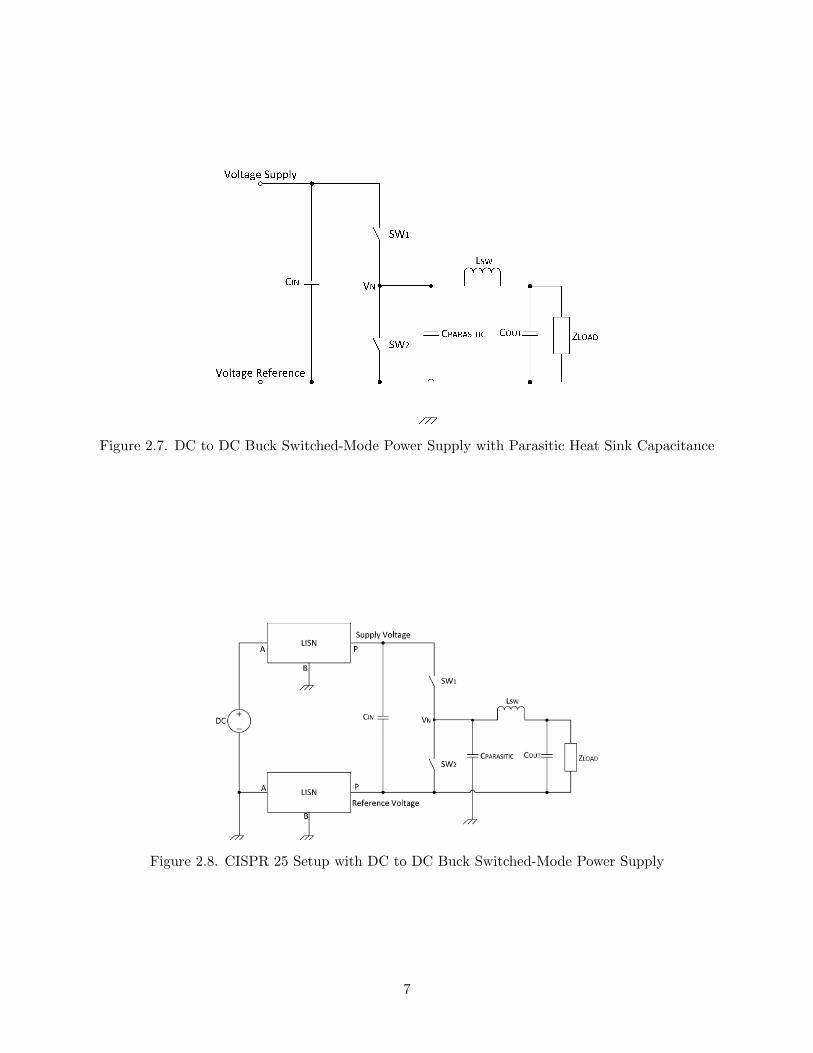
Figure 2.7. DC to DC Buck Switched-Mode Power Supply with Parasitic Heat Sink Capacitance
Figure 2.8. CISPR 25 Setup with DC to DC Buck Switched-Mode Power Supply
7
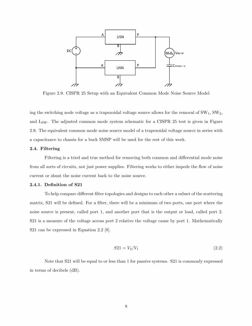
Figure 2.9. CISPR 25 Setup with an Equivalent Common Mode Noise Source Model
ing the switching node voltage as a trapezoidal voltage source allows for the removal of SW1, SW2,
and LSW. The adjusted common mode system schematic for a CISPR 25 test is given in Figure
2.9. The equivalent common mode noise source model of a trapezoidal voltage source in series with
a capacitance to chassis for a buck SMSP will be used for the rest of this work.
2.4. Filtering
Filtering is a tried and true method for removing both common and differential mode noise
from all sorts of circuits, not just power supplies. Filtering works to either impede the flow of noise
current or shunt the noise current back to the noise source.
2.4.1. Definition of S21
To help compare different filter topologies and designs to each other a subset of the scattering
matrix, S21 will be defined. For a filter, there will be a minimum of two ports, one port where the
noise source is present, called port 1, and another port that is the output or load, called port 2.
S21 is a measure of the voltage across port 2 relative the voltage cause by port 1. Mathematically
S21 can be expressed in Equation 2.2 [8].
S21 = V2/V1 (2.2)
Note that S21 will be equal to or less than 1 for passive systems. S21 is commonly expressed
in terms of decibels (dB).
8

Figure 2.10. Traditional Power Supply Filter
2.4.2. Traditional Filtering
A traditional power supply filter for passing either a conducted or radiated emissions test is
shown in Figure 2.10 [2, 3]. Topologies do vary, but the filter in Figure 2.10 has all of the traditional
elements.
In a simple two conductor DC power feed there will be both a power supply line and power
return. In Figure 2.10, the Cdm are capacitors for filtering differential mode noise on the power
supply lines. Similarly, Ldm is an inductor also used for filtering differential mode noise on the
power supply lines. The Ccm, are common mode capacitors used for filtering common mode noise
on the power supply lines. Ccm differ from Cdm in that they are connected generally to a chassis
or earth ground. Common mode capacitors are often limited in capacitance due to different design
requirements, usually involving safety and needing to isolate the power supply lines from chassis
or earth ground. Lcm is a common mode inductor, or a common mode choke, used for filtering
common mode noise from the power supply lines. For a traditional power supply filter the common
mode choke is often the largest component, due to the limited capacitance of the common mode
capacitors. Depending on the power required and the frequency of suppression needed a costly
custom common mode choke may be required. As SMPS continue to increase in frequency and in
power, the common mode choke will continue to make up a large portion of the total system cost
and size [9].
2.4.3. Active Filtering
In contrast to using a large traditional power supply filter, an active filter can be used
to replace or supplement the existing common mode choke. As discussed in previous research,
there are four basic topologies for active power supply filtering [10]: Current Sensing Current
9
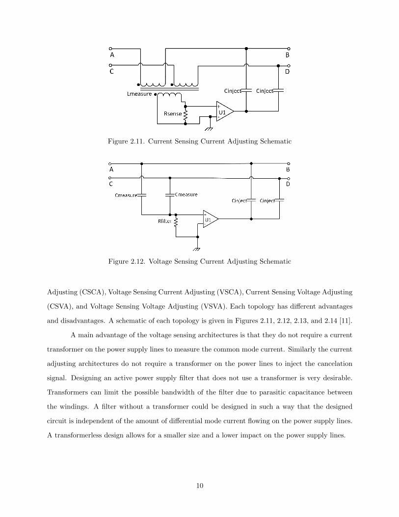
Figure 2.11. Current Sensing Current Adjusting Schematic
Figure 2.12. Voltage Sensing Current Adjusting Schematic
Adjusting (CSCA), Voltage Sensing Current Adjusting (VSCA), Current Sensing Voltage Adjusting
(CSVA), and Voltage Sensing Voltage Adjusting (VSVA). Each topology has different advantages
and disadvantages. A schematic of each topology is given in Figures 2.11, 2.12, 2.13, and 2.14 [11].
A main advantage of the voltage sensing architectures is that they do not require a current
transformer on the power supply lines to measure the common mode current. Similarly the current
adjusting architectures do not require a transformer on the power lines to inject the cancelation
signal. Designing an active power supply filter that does not use a transformer is very desirable.
Transformers can limit the possible bandwidth of the filter due to parasitic capacitance between
the windings. A filter without a transformer could be designed in such a way that the designed
circuit is independent of the amount of differential mode current flowing on the power supply lines.
A transformerless design allows for a smaller size and a lower impact on the power supply lines.
10

Figure 2.13. Current Sensing Voltage Adjusting Schematic
Figure 2.14. Voltage Sensing Voltage Adjusting Schematic
11

Figure 2.15. Proposed Voltage Sensing Voltage Adjusting Schematic
2.4.4. Voltage Sensing Current Adjusting Architecture
Previously, the work in [11] examined a transformerless active filter designed to operate in
the region between 150kHz-30MHz. It showed that a transformerless design can be stable over a
very large range of both source and load impedances. To achieve filtering above 2MHz, the design
reported in [11] used passive components and did not rely on the active circuit. Similarly, the work
reported in [12] also designed a transformerless active filter. They showed that a great amount of
cost savings and size reduction can be achieved using an active filter. Again though, their maximum
active filter frequency was limited to 2MHz.
A schematic of a potential VSCA filter for use with a DC to DC SMSP is given in Figure
2.15. Notice the voltage measuring stage of the filter consists of two capacitors, Cmeasure. These
capacitors block any DC voltage and allow common mode AC noise to pass to the inverting input
of the amplifier. The amplifier then uses the feedback network, Zfeedback, to create a cancelation
signal, and injects that signal into the power supply lines through Cinject. Cinject also serves the
purpose of protecting the output from the DC voltage on the supply lines.
Note that in this design, the non-inverting input of the amplifier is connected to the chassis.
To help satisfy any potential safety concerns, it is important that the amplifier be powered from
isolated power supplies and the capacitors in the circuit be safety rated Y capacitors. A Y capacitor
is a special type of high reliability capacitor that is designed to fail open rather than fail short.
This helps to protect consumers from the potentially dangerous power supply voltage in case of
failure.
12

Figure 2.16. VSCA Filter in System Application
To balance the common mode correction signal properly, it is important that Cinject be the
same capacitance value and low tolerance. Any mismatch in the injection capacitors will cause
error in the output. Optimal values for these capacitors and other components for the circuit given
in Figure 2.15 will be presented in Chapter 3.
Careful examination of the circuit in Figure 2.15 will reveal that any high frequency differ-
ential mode voltage noise on the power supply lines will be presented at the non-inverting of the
amplifier. In order to prevent the filter from measuring and responding to high frequency differen-
tial mode noise, a high frequency differential mode filter should be added before the input of the
VSCA filter. A block diagram of schematic of a system using this VSCA filter is given in Figure
2.16. It is worthwhile to note that a practical SMSP design will already contain a differential mode
filter for the power supply lines. The differential mode filter is given in Figure 2.7 as Cin.
13

CHAPTER 3. RESULTS
3.1. Introduction
Chapter 3 discusses one potential solution to the problem of conducted and radiated emis-
sions presented in Chapter 2. The proposed filter at the end of Chapter 2 is expanded upon,
analyzed, and synthesized. Simulations are conducted to predict real world performance. S21,
frequency domain, and time domain measurements of a test filter with several possible feedback
configurations are presented.
3.2. Analysis of Proposed Active Filter
To begin analyzing the VSCA active filter proposed in Chapter 2, it will first be assumed
that the noise source the circuit is trying to filter is the common mode noise from a SMPS. The
combined circuit of Figure 2.15, the equivalent common mode noise source of a SMPS, and a
common mode load is shown in Figure 3.1. The equivalent common mode noise source impedance
is labeled as Zsource in Figure 3.1. The common mode load, ZLISN, represents the LISNs used as
part of the measurement setup in a standard test, such as CISPR 25.
3.2.1. Transfer Function
Using nodal analysis and the properties of an ideal op-amp, a function for voltage across
ZLISN(s) from the circuit shown in Figure 3.1 was derived and is given in 3.1. This transfer function
can be used to help find the ideal feedback network with an ideal op-amp. Using 3.1, assuming
a source impedance, Zsource(s), of a 200pF capacitor in series with 50Ω resistor, and a 50Ω LISN
impedance, the voltage across ZLISN is plotted using MATLAB in Figure 3.2 a feedback network in
which Zfeedback is 1GΩ, a feedback network in which Zfeedback is 0Ω and a feedback in which Zfeedback
is 100Ω. Figure 3.2 shows that a 1GΩ feedback network should have the lowest voltage across the
LISN, while a 0Ω feedback network is has a similar voltage across the LISN as a 100Ω feedback up
until about 2MHz. After 2MHz the 100Ω feedback outperforms the 0Ω feedback network. For all
of the MATLAB calculations Cmeasure and Cinject were taken to be 1nF capacitors.
3.2.2. Determination of Zfeedback
From 3.1 it can clearly be seen that the best feedback configuration for the ideal op-amp
is when the feedback network is open. Examining 3.1 shows that this makes sense. The lowest
14

VLISN (s)
Vsource(s)=
1( 1
Zsource(s)+
2
Zmeasure(s)+
2
Zinject(s)+
4 · Zfeedback(s)
(Zmeasure(s) ∗ Zinject(s))+
1
ZLISN (s)
) ·1
Zsource(s)
(3.1)
Figure 3.1. System schematic with proposed VSCA filter for analysis
0.1 1.0 10.0 100.0Frequency (MHz)
-220
-200
-180
-160
-140
-120
-100
-80
-60
-40
-20
0
|S21
| (dB
)
Short100Ω1GΩ
Figure 3.2. MATLAB plot of voltage across the LISN impedance predicted by 3.1 using threepossible feedback configurations, a shorted feedback network, a 100Ω feedback network, and a 1GΩfeedback network.
15

0.1 1.0 10.0 100.0Frequency (MHz)
-220
-200
-180
-160
-140
-120
-100
-80
-60
-40
-20
0
|S21
| (dB
)
ShortFour 1nF Capacitors
Figure 3.3. MATLAB plot comparing four 1nF capacitors connected in parallel with ZLISN toproposed filter with shorted feedback.
common mode voltage across the LISN will be as VLISN(s)/Vsource(s) approaches zero. By holding
all other values constant, the best way to get VLISN(s)/Vsource(s) to approach zero is to increase
Zfeedback(s). For an ideal op-amp, the best feedback network is an open circuit.
Contrastingly, examining 3.1 shows the worst performing feedback network is a short circuit.
Again this result makes intuitive sense. For an ideal op-amp, the output of op-amp would simply
be the chassis reference voltage at the inverting input, since the output and the non-inverting input
are tied together. In essence this feedback network does not take advantage of the voltage gain the
amplifier can provide. While the current flowing to the chassis is relatively small for the filter circuit
with a shorted feedback network, the calculated voltage across ZLISN is the same as connecting 2
Cmeasure and 2 Cinject capacitors to chassis reference. This result is shown in Figure 3.3, where a
comparison of an ideal short feedback network with an ideal op-amp is compared to a filter with
four 1nF filtering capacitors.
16

0.1 1.0 10.0 100.0Frequency (MHz)
-50
-45
-40
-35
-30
-25
-20
-15
-10
-5
0
|S21
| (dB
)
MATLAB ShortSimulate Short
Figure 3.4. Plot of S21 comparing MATLAB code using 3.1 to Keysight ADS simulation usingideal an op-amp and a shorted feedback network.
3.2.3. Ideal Simulation
As part of the design, the circuit was simulated using Keysight”s ADS 2015 [13]. First the
circuit was simulated using an ideal op-amp model. For the simulation an S-parameter sweep was
conducted. The results for an ideal op-amp with a shorted feedback network are given in Figure
3.4 and are compared to the MATLAB results given for 3.1. Similarly, the results for a simulation
with a 100Ω feedback network are given in Figure 3.5. Finally, the results for a simulation with an
open feedback network are given in Figure 3.6, where the MATLAB comparison uses a feedback
resistor of 1GΩ. From Figures 3.4, 3.5, and 3.6, it is shown that ADS simulation with and ideal
op-amp closely matches the MATLAB results for 3.1. The only noticeable difference is that the
open configuration does not filter as much as the 1GΩ feedback. This is a result of the op-amp in
ADS having a gain of 10,000 and an ideal op-amp having an infinite gain.
3.2.4. Bandwidth Limited Simulation
Next, simulations were done with a non-ideal, bandwidth limited op-amp. Figure 3.7 shows
the simulation schematic in ADS with a 100Ω feedback network. For these simulations a 400MHz
17

0.1 1.0 10.0 100.0Frequency (MHz)
-50
-45
-40
-35
-30
-25
-20
-15
-10
-5
0
|S21
| (dB
)
MATLAB 100ΩSimulate 100Ω
Figure 3.5. Plot of S21 comparing MATLAB code using 3.1 to Keysight ADS simulation usingideal an op-amp and a 100Ω feedback network.
bandwidth was selected for the bandwidth limited model and a slew rate of 950V/µs were used.
The gain on the op-amp was set to 60dB. Using an S-parameter sweep the results for a shorted
feedback network, a 100Ω network, and an open feedback network are given in Figure 3.8.
The results of the bandwidth limited simulation are interesting because they begin to show
how a bandwidth limited op-amp will respond. Comparing the 100Ω feedback network bandwidth
limited simulation and MATLAB results using 3.1 are done in Figure 3.9. From the graph it can
be seen that the non-ideal bandwidth limited op-amp has more loss than the results predicted by
3.1 between 10MHz and 24MHz. This effect wears off as frequency increases and the bandwidth
limited amplifier is out performed by 3.1 after 24MHz.
Looking more closely at the differences between the ideal and bandwidth limited op amp
circuits with a 100Ω feedback network, a comparison of the voltage magnitude on the output of the
op amps is given in Figure 3.10. The voltage magnitudes look to match very closely, the differences
in the S21 simulated values does not appear to be explained by the magnitude of the voltage output
by the op amps.
18

0.1 1.0 10.0 100.0Frequency (MHz)
-220
-200
-180
-160
-140
-120
-100
-80
-60
-40
-20
0
|S21
| (dB
)
MATLAB 1GΩSimulate OPEN
Figure 3.6. Plot of S21 comparing MATLAB code using 3.1 with 1GΩ feedback network to KeysightADS simulation using an ideal op-amp with a gain of 10000 and an open feedback network.
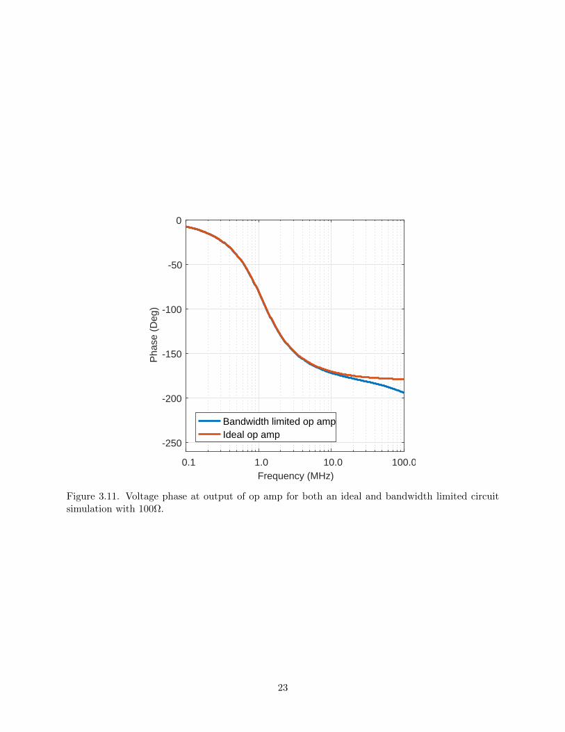
Figure 3.11 is a voltage phase plot comparing the op amp outputs over frequency for the
100Ω feedback network. The phase difference shows that the bandwidth limited op amp is not
able to keep up with the ideal on amp. This causes a lagging phase, and it appears to be this
phase difference that causes the bandwidth limited op amp to outperform the ideal op amp up to
a certain frequency. As frequency continues to increase the bandwidth limited amplifier continues
to have its output lag and eventually the ideal op amp outperforms it.
Exploring the difference between the ideal and the bandwidth limted model for the op-amp
shows the limitation of 3.1. The effect of op-amp bandwidth is reinforced in Figure 3.12, where the
100Ω feedback circuit is simulated with multiple bandwidths (100MHz, 200MHz, and 400MHz).
From Figure 3.12 shows that selecting an op-amp with higher bandwidth should filter out higher
frequencies.
3.3. Filter Synthesis
The op-amp selected for this circuit was a Texas Instrument’s THS4271. The THS4271 was
selected because of its large bandwidth (380MHz), dual 5V supply rail operation, and its low output
19
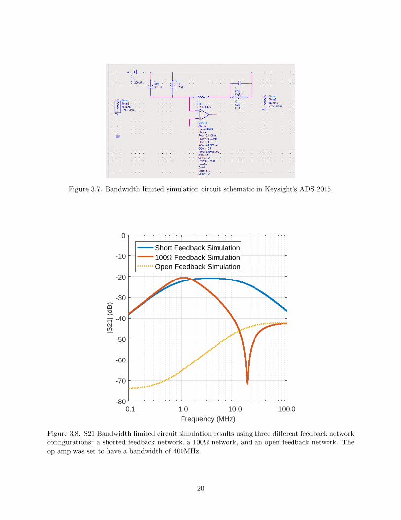
Figure 3.7. Bandwidth limited simulation circuit schematic in Keysight’s ADS 2015.
0.1 1.0 10.0 100.0Frequency (MHz)
-80
-70
-60
-50
-40
-30
-20
-10
0
|S21
| (dB
)
Short Feedback Simulation100Ω Feedback SimulationOpen Feedback Simulation
Figure 3.8. S21 Bandwidth limited circuit simulation results using three different feedback networkconfigurations: a shorted feedback network, a 100Ω network, and an open feedback network. Theop amp was set to have a bandwidth of 400MHz.
20

0.1 1.0 10.0 100.0Frequency (MHz)
-80
-70
-60
-50
-40
-30
-20
-10
0
|S21
| (dB
)
MATLAB 100ΩSimulate 100Ω
Figure 3.9. Results of S21 bandwidth limited circuit simulation with 100Ω feedback compared toMATLAB predicted results using 3.1 with a 100Ω feedback configuration.
21

0.1 1.0 10.0 100.0Frequency (MHz)
-0.02
0
0.02
0.04
0.06
0.08
0.1
|Vol
tage
| (V
)
Bandwidth limited op ampIdeal op amp
Figure 3.10. Voltage magnitude at output of op amp for both an ideal and bandwidth limitedcircuit simulation with 100Ω.
22
0.1 1.0 10.0 100.0Frequency (MHz)
-250
-200
-150
-100
-50
0
Pha
se (
Deg
)
Bandwidth limited op ampIdeal op amp
Figure 3.11. Voltage phase at output of op amp for both an ideal and bandwidth limited circuitsimulation with 100Ω.
23

0.1 1.0 10.0 100.0Frequency (MHz)
-80
-70
-60
-50
-40
-30
-20
-10
0
|S21
| in
dB
100MHz BW200MHz BW400MHz BW
Figure 3.12. Circuit simulation with 100Ω feedback and a bandwidth limited op-amp with threedifferent bandwidths, 100MHz, 200MHz, and 400MHz.
24

Figure 3.13. Photo of designed circuit. A quarter is given for size comparison.
impedance [14]. The op-amp was supplied with a +5V and -5V power rail and was decoupled with
a 0.1µF capacitor on the power supply input pins. The large bandwidth of the op-amp was selected
to be sure that the frequency response does not roll off before our desired cut-off frequency. The
circuit was built on a printed circuit board and is pictured in Figure 3.13. For the circuit a variety of
feedback networks were tested, but Cmeasure and Cinject were taken to be 1nF Y-rated capacitors. A
full schematic of the designed filter circuit is given in Figure 3.14. The differential mode capacitors
(C5-C8) were 1nF capacitors.
3.4. Measurements
3.4.1. S21 Measurment
For the S21 measurements Keysight”s E5071C Network Analyzer was used. The power
level on the network analyzer was set to 10dBm and the circuit was powered by +5V and -5V. A
schematic of the test setup is given in Figure 3.15. First the circuit with three different feedback
networks were measured. The feedback networks included a shorted feedback network, a feedback
network with a 100Ω resistor, and an open feedback network. In addition, a circuit consisting of
four in parallel 1nF capacitors connected to chassis was also measured. These measurements are
given in Figure 3.16.
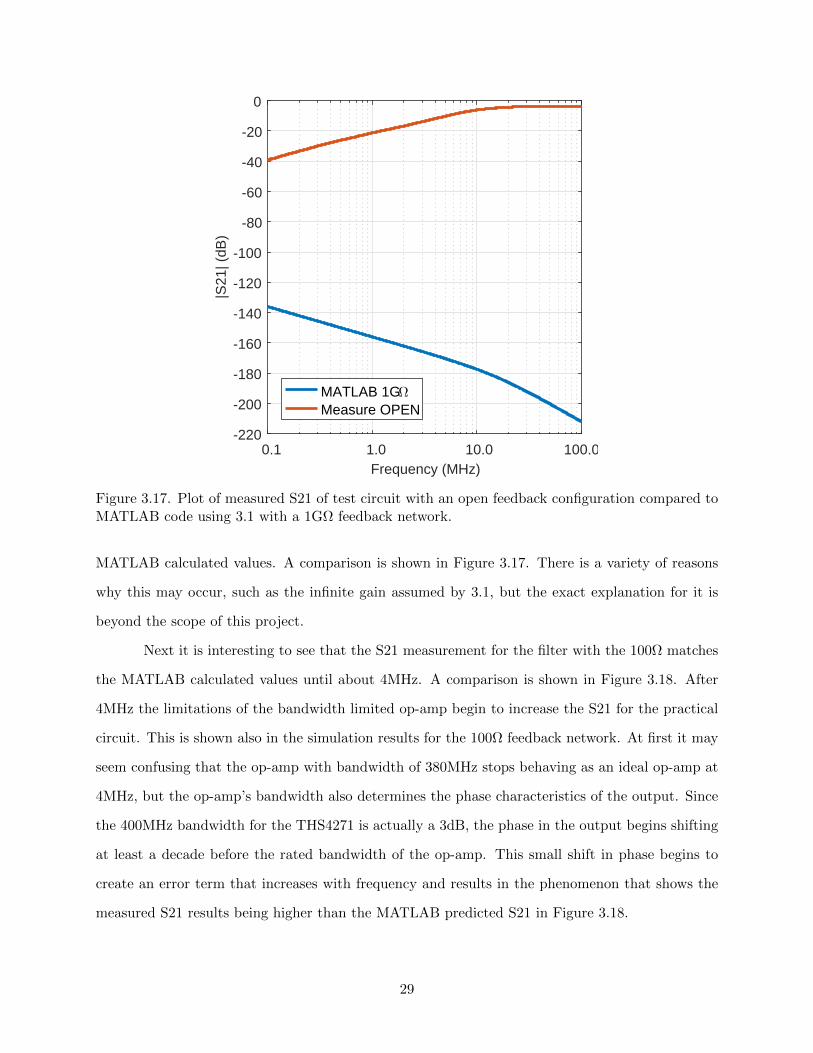
The S21 measurements show a variety of interesting phenomenon. First it is interesting to
see that the S21 measurement for the filter with the open feedback network differs greatly from the
25
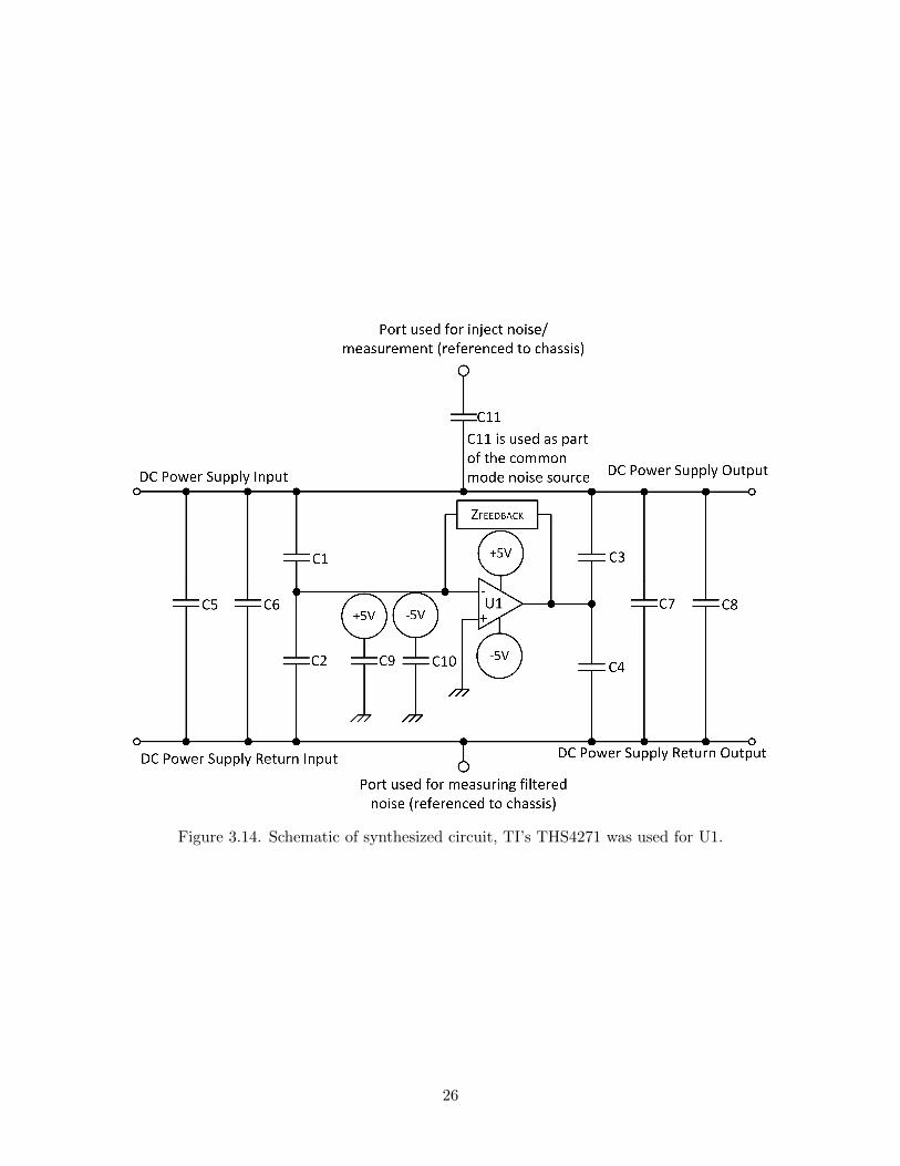
Figure 3.14. Schematic of synthesized circuit, TI’s THS4271 was used for U1.
26
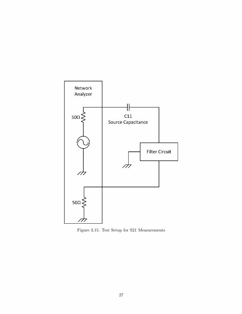
Figure 3.15. Test Setup for S21 Measurements
27

0.1 1.0 10.0 100.0Frequency (MHz)
-60
-50
-40
-30
-20
-10
0
|S21
| (dB
)
100ΩShortOpenCapacitors OnlyNo Filter
Figure 3.16. Plot of S21 with a 10dBm source applied to circuits under test with a 50Ω resistor inseries with a 220pF capacitor as source impedance. The test circuit uses three different possiblefeedback networks, a shorted network, an open network, and an open circuit network. The plotcompares the active filter to four 1nF capacitors and a setup with no filter present.
28
0.1 1.0 10.0 100.0Frequency (MHz)
-220
-200
-180
-160
-140
-120
-100
-80
-60
-40
-20
0
|S21
| (dB
)
MATLAB 1GΩMeasure OPEN
Figure 3.17. Plot of measured S21 of test circuit with an open feedback configuration compared toMATLAB code using 3.1 with a 1GΩ feedback network.
MATLAB calculated values. A comparison is shown in Figure 3.17. There is a variety of reasons
why this may occur, such as the infinite gain assumed by 3.1, but the exact explanation for it is
beyond the scope of this project.
Next it is interesting to see that the S21 measurement for the filter with the 100Ω matches
the MATLAB calculated values until about 4MHz. A comparison is shown in Figure 3.18. After
4MHz the limitations of the bandwidth limited op-amp begin to increase the S21 for the practical
circuit. This is shown also in the simulation results for the 100Ω feedback network. At first it may
seem confusing that the op-amp with bandwidth of 380MHz stops behaving as an ideal op-amp at
4MHz, but the op-amp’s bandwidth also determines the phase characteristics of the output. Since
the 400MHz bandwidth for the THS4271 is actually a 3dB, the phase in the output begins shifting
at least a decade before the rated bandwidth of the op-amp. This small shift in phase begins to
create an error term that increases with frequency and results in the phenomenon that shows the
measured S21 results being higher than the MATLAB predicted S21 in Figure 3.18.
29
0.1 1.0 10.0 100.0Frequency (MHz)
-50
-45
-40
-35
-30
-25
-20
-15
-10
-5
0
|S21
| (dB
)
MATLAB 100ΩMeasure 100Ω
Figure 3.18. Plot of measured S21 of test circuit with a 100Ω feedback configuration compared toMATLAB code using 3.1 with a 100Ω feedback network.
30
0.1 1.0 10.0 100.0Frequency (MHz)
-50
-45
-40
-35
-30
-25
-20
-15
-10
-5
0
|S21
| (dB
)
Measure 100Ω FeedbackMeasure Four 1nF Capacitors
Figure 3.19. Plot of measured S21 of test circuit with a 100Ω feedback configuration compared tomeasured S21 of circuit using four 1nF capacitors connected in parallel.
Also it is interesting now to compare the filter with 100Ω feedback to the measured value
of four 1nF capacitors. A plot of this is given in Figure 3.19. From the plot it can be seen that
the active filter performs better than a strictly passive filter from roughly 2MHz to 10MHz. From
Figure 3.19 the largest difference was found to be about 6dB.
Finally, the filter measurements with the shorted feedback network will be compared to
the original MATLAB code. A comparison of the measurement to the MATLAB values is given
in Figure 3.20. The measurements agree closely with the original MATLAB code up until about
7MHz. After 7MHz the bandwidth limitations of the op-amp again take over and it can be seen
that they decrease the S21 until about 15MHz and then the S21 begins increasing again. The
reasoning for this phenomenon is the same as the for the 100Ω feedback case.
Again it is worthwhile to compare the measured results of the circuit with a shorted feedback
network to the measured results of the circuit with four 1nF capacitors. These are compared in
Figure 3.21. Comparing the measurements shows that the shorted feedback network provides a
greater loss than the purely passive filter between 4MHz and 20MHz, the greatest difference is
31
0.1 1.0 10.0 100.0Frequency (MHz)
-50
-45
-40
-35
-30
-25
-20
-15
-10
-5
0
|S21
| (dB
)
MATLAB ShortMeasure Short
Figure 3.20. Plot of measured S21 of test circuit with a shorted feedback configuration comparedto MATLAB code using 3.1 with a shorted feedback network.
32

0.1 1.0 10.0 100.0Frequency (MHz)
-50
-45
-40
-35
-30
-25
-20
-15
-10
-5
0
|S21
| (dB
)
Measured Shorted FeedbackMeasured Four 1nF Capacitors Filter
Figure 3.21. Plot of measured S21 of test circuit with a shorted feedback configuration comparedto measured S21 of circuit using four 1nF capacitors connected in parallel.
measured to be 25dB. This is a very large difference that shows promise for the active filter in this
frequency range.
It is prudent now to compare the difference between the 100Ω and the shorted feedback
network. A comparison is given in Figure 3.22. Both configurations have a considerably large range
of frequencies where they perform better than a purely passive filter. It is interesting to note how
the 100Ω feedback appears to shift the active filter band lower while also decreasing the filter’s
maximum effectiveness. This seems to indicate that different resistor values could be used to tune
the filter to filter specific frequencies between 2MHz and 14MHz.
3.4.2. Frequency Domain
For the frequency domain measurements the circuit was driven by Keysight”s 81160A Pulse
Function Arbitrary Generator, set to output a 50% duty cycle 3V peak to peak 1MHz square wave
with 1ns rise and fall times. The spectral measurements were taken with Keysight”s E4402B
Spectrum Analyzer. The setup for frequency domain measurements are shown in Figure 3.23.
33
0.1 1.0 10.0 100.0Frequency (MHz)
-50
-45
-40
-35
-30
-25
-20
-15
-10
-5
0
|S21
| (dB
)
Measured Shorted FeedbackMeasured 100Ω Feedback
Figure 3.22. Plot of measured S21 of test circuit with a shorted feedback configuration comparedto measured S21 of test circuit using a 100Ω feedback configuration.
34

Figure 3.23. Test setup for time and frequency measurements.
35

2 4 6 8 10 12 14 16 18 20
Frequency (MHz)
50
60
70
80
90
100
110
120
130
140
|ZL
ISN
Vol
tage
| (d
Bµ
V)
No Filter100ΩOpenCapacitors OnlyShort
Figure 3.24. Plot of spectral measurements with a 1MHz square wave applied to circuits undertest with a 50Ω resistor in series with a 220pF capacitor as source impedance. The input waveformwas 3V peak to peak. The proposed filter circuit was tested with a shorted feedback configuration,100Ω feedback configuration, and open feedback configuration. The proposed filter measurementsare also compared to four 1nF capacitors in parallel and a test setup without a filter.
Similar to the S21 measurements, three different feedback networks were measured. The
feedback networks included a shorted feedback network, a feedback network with a 100Ω resistor,
and an open feedback network. Again, a circuit consisting of four in parallel 1nF capacitors and
connected to chassis was also measured. The results between 500kHz and 20.5MHz are shown in
Figure 3.24.
Figure 3.24 shows that the active filter performs significantly better than using four capac-
itors for common mode filtering at some frequencies in the 1MHz to 20MHz band. Interestingly,
while the open feedback network was thought to be the best from a theoretical standpoint, when
tested with an actual noise input, it provided less than 4dB of filtering over not using any filter.
Additionally the open feedback configuration actually increased the levels of the even harmonics
and caused the design to become more noisy. Based on these results, using an open feedback con-
figuration would not be recommended. The 100Ω feedback configuration outperformed the four
1nF capacitors from 3MHz to 9MHz. This agrees with the S21 results showing that the feedback
configuration outperformed the four 1nF capacitors between 2Mhz and 10MHz. Looking at the
performance of the shorted feedback network, the shorted feedback network out performs the four
1nF capacitors from 7MHz until 17MHz. Note that now a difference is seen between the S21
measurements and the frequency domain measurement. Specifically at 19MHz the active filter
36
10 20 30 40 50 60 70 80
Frequency (MHz)
50
60
70
80
90
100
110
120
130
140
|ZL
ISN
Vol
tage
| (d
Bµ
V)
No Filter100ΩOpenCapacitors OnlyShort
Figure 3.25. Plot of spectral measurements using the same setup as Figure 3.24, except with alarger frequency band shown.
measurement is a couple of dB higher than the four 1nF capacitors. This is important information
to consider when designing an active common mode filter.
Figure 3.25 shows the response of the filter at frequencies even higher than 20MHz. The
limitations of an active filter become very evident. After 20MHz the four 1nF capactior passive
filter, easily out performs the active filter. The active filter configuration appears to converge to
a single value and are indistinguishable at about 65MHz. To overcome this limitation it may be
wise to consider adding passive filter elements for frequencies above 20MHz. Adding additional
passive filter elements does not uncut the advantages of using an active filter. The active filter still
provides additional filtering at frequencies below 20MHz and greatly reduces currently flowing on
the chassis.
3.4.3. Time Domain
The final measurements of the proposed active VSCA common mode filter are time domain
measurements of the filter output. For these measurements the same setup was used as for the
frequency domain measurements. 1MHz 3V peak to peak square wave was applied to the circuit
as a noise source. Refer to Figure 3.23 for a schematic of the setup. Figure 3.26 shows the time
domain measurements over multiple periods. Figure 3.27 shows the time domain measurement
zoomed in around a rising edge on the input waveform.
Reviewing Figure 3.27 gives an intuitive feel for how the active filter performs. The open
feedback follows the output with no filter very closely with only amplitude differences. The short
and 100Ω feedback configurations follow each other closely. It can be seen that the active filter still
37
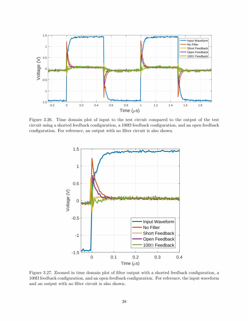
-0.2 0 0.2 0.4 0.6 0.8 1 1.2 1.4 1.6 1.8
Time (µs)
-1.5
-1
-0.5
0
0.5
1
1.5V
olta
ge (
V)
Input WaveformNo FilterShort FeedbackOpen Feedback100Ω Feedback
Figure 3.26. Time domain plot of input to the test circuit compared to the output of the testcircuit using a shorted feedback configuration, a 100Ω feedback configuration, and an open feedbackconfiguration. For reference, an output with no filter circuit is also shown.
0 0.1 0.2 0.3 0.4Time (µs)
-1.5
-1
-0.5
0
0.5
1
1.5
Vol
tage
(V
)
Input WaveformNo FilterShort FeedbackOpen Feedback100Ω Feedback
Figure 3.27. Zoomed in time domain plot of filter output with a shorted feedback configuration, a100Ω feedback configuration, and an open feedback configuration. For reference, the input waveformand an output with no filter circuit is also shown.
38

has a lot of high frequency content by the sharp transitions and that some of the low frequency
content has been removed by noticing that the decay after the rising edge has been removed.
39
CHAPTER 4. CONCLUSION
In this thesis, a voltage sensing current adjusting active common mode filter was presented.
The proposed filter was designed for DC to DC switched mode power supplies with current draw
requirements too large for traditional common mode chokes to be cost effective. The proposed
design was analyzed theoretically, simulated, synthesized, and measured. The measured S21 results
showed active filtering at 20MHz, much greater than previous designs. The filter also reduces the
current measured on chassis connections caused by parasitic capacitance. Measured spectral results
with the filter using a 1MHz waveform shows that the active filter outperforms a purely passive
filter constructed of similar components over the design frequency range. Several possible filter
feedback configurations were analyzed. The study suggests that optimal feedback configurations
are not straightforward, but can be tuned in using measurements.
The proposed filter could be used in a variety of applications that cannot use traditional
power supply filters. The designed filter can be made to work with power supply system independent
of the power supply design current. The filter offers a much smaller and more convenient alternative
to common mode choke.
40
BIBLIOGRAPHY
[1] L. Roslaniec, A. Jurkov, A. Bastami, and D. Perreault, “Design of single-switch inverters for
variable resistance/load modulation operation,” Power Electronics, IEEE Transactions on,
vol. 30, no. 6, pp. 3200–3214, June 2015.
[2] H. Ott, Electromagnetic Compatibility Engineering. Wiley, 2011. [Online]. Available:
https://books.google.com/books?id=2-4WJKxzzigC
[3] C. R. Paul, Introduction to Electromagnetic Compatibility (Wiley Series in Microwave and
Optical Engineering). Wiley-Interscience, 2006.
[4] CISPR 25: Limits and methods of measurement of radio disturbance characteristics for pro-
tection of receivers used on board vehicles, Comite International Special des Perturbations
Radioelectriques Std., Rev. 3rd., 2008.
[5] S. Wang and F. Lee, “Common-mode noise reduction for power factor correction circuit
with parasitic capacitance cancellation,” Electromagnetic Compatibility, IEEE Transactions
on, vol. 49, no. 3, pp. 537–542, Aug 2007.
[6] G. W. Wester and R. D. Middlebrook, “Low-frequency characterization of switched dc-dc
converters,” IEEE Transactions on Aerospace and Electronic Systems, vol. AES-9, no. 3, pp.
376–385, May 1973.
[7] M. H. Nagrial and A. Hellany, “Emi/emc issues in switch mode power supplies (smps),” in
Electromagnetic Compatibility, 1999. EMC York 99. International Conference and Exhibition
on (Conf. Publ. No. 464), July 1999, pp. 180–185.
[8] D. M. Pozar, Microwave Engineering, 4th ed. Wiley, 2012.
[9] Fairites. How to choose ferrite components for emi suppression. [Online]. Available:
www.fair-rite.com
41

[10] L. E. Lawhite and M. Schlecht, “Active filters for 1-mhz power circuits with strict input/output
ripple requirements,” Power Electronics, IEEE Transactions on, vol. PE-2, no. 4, pp. 282–290,
Oct 1987.
[11] M. Heldwein, H. Ertl, J. Biela, and J. Kolar, “Implementation of a transformerless common-
mode active filter for offline converter systems,” Industrial Electronics, IEEE Transactions on,
vol. 57, no. 5, pp. 1772–1786, May 2010.
[12] A. Chow and D. Perreault, “Active emi filters for automotive motor drives,” in Power Elec-
tronics in Transportation, 2002, Oct 2002, pp. 127–134.
[13] Advanced Computer Design, Ads 2015 ed., Keysight Technologies Inc.
[14] T. I. Inc. Low noise, high slew rate, unity gain stable voltage feedback amplifier. [Online].
Available: www.ti.com
42
APPENDIX
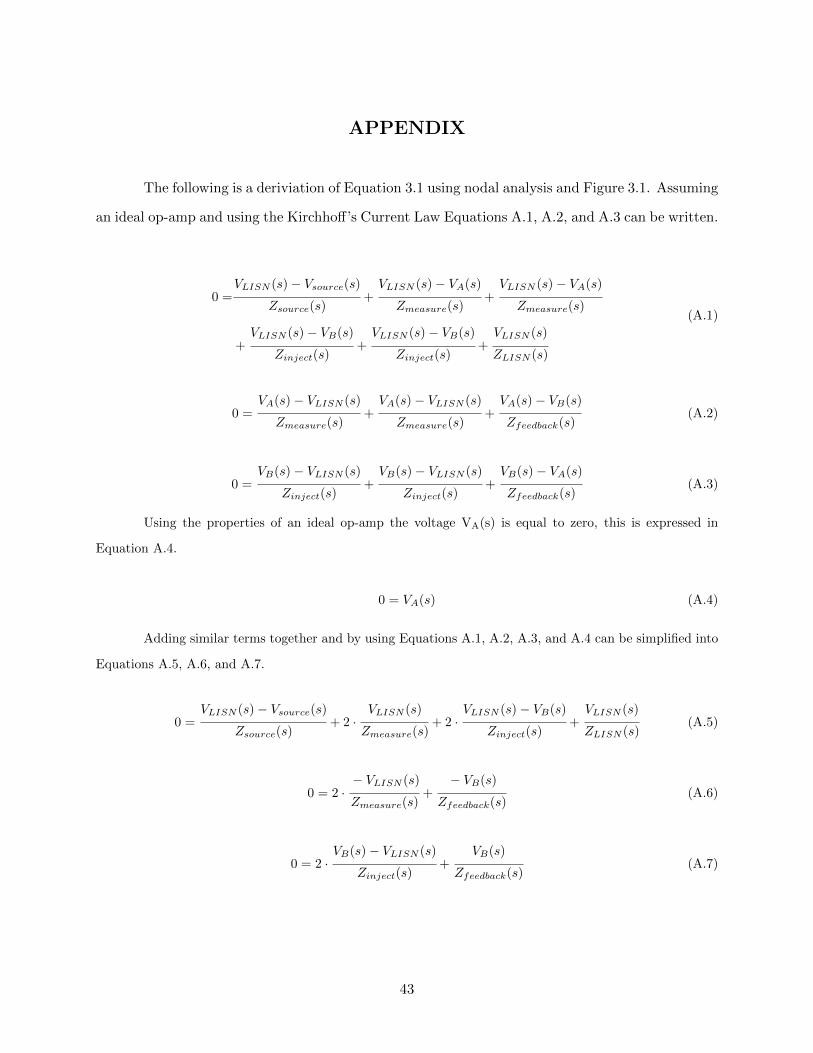
The following is a deriviation of Equation 3.1 using nodal analysis and Figure 3.1. Assuming
an ideal op-amp and using the Kirchhoff’s Current Law Equations A.1, A.2, and A.3 can be written.
0 =VLISN (s) − Vsource(s)
Zsource(s)+VLISN (s) − VA(s)
Zmeasure(s)+VLISN (s) − VA(s)
Zmeasure(s)
+VLISN (s) − VB(s)
Zinject(s)+VLISN (s) − VB(s)
Zinject(s)+VLISN (s)
ZLISN (s)
(A.1)
0 =VA(s) − VLISN (s)
Zmeasure(s)+VA(s) − VLISN (s)
Zmeasure(s)+VA(s) − VB(s)
Zfeedback(s)(A.2)
0 =VB(s) − VLISN (s)
Zinject(s)+VB(s) − VLISN (s)
Zinject(s)+VB(s) − VA(s)
Zfeedback(s)(A.3)
Using the properties of an ideal op-amp the voltage VA(s) is equal to zero, this is expressed in
Equation A.4.
0 = VA(s) (A.4)
Adding similar terms together and by using Equations A.1, A.2, A.3, and A.4 can be simplified into
Equations A.5, A.6, and A.7.
0 =VLISN (s) − Vsource(s)
Zsource(s)+ 2 ·
VLISN (s)
Zmeasure(s)+ 2 ·
VLISN (s) − VB(s)
Zinject(s)+VLISN (s)
ZLISN (s)(A.5)
0 = 2 ·− VLISN (s)
Zmeasure(s)+
− VB(s)
Zfeedback(s)(A.6)
0 = 2 ·VB(s) − VLISN (s)
Zinject(s)+
VB(s)
Zfeedback(s)(A.7)
43
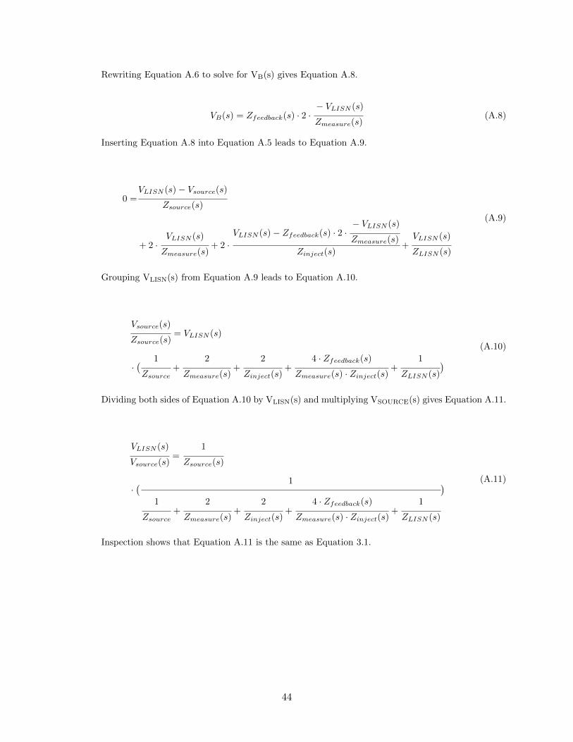
Rewriting Equation A.6 to solve for VB(s) gives Equation A.8.
VB(s) = Zfeedback(s) · 2 ·− VLISN (s)
Zmeasure(s)(A.8)
Inserting Equation A.8 into Equation A.5 leads to Equation A.9.
0 =VLISN (s) − Vsource(s)
Zsource(s)
+ 2 ·VLISN (s)
Zmeasure(s)+ 2 ·
VLISN (s) − Zfeedback(s) · 2 ·− VLISN (s)
Zmeasure(s)
Zinject(s)+VLISN (s)
ZLISN (s)
(A.9)
Grouping VLISN(s) from Equation A.9 leads to Equation A.10.
Vsource(s)
Zsource(s)= VLISN (s)
·( 1
Zsource+
2
Zmeasure(s)+
2
Zinject(s)+
4 · Zfeedback(s)
Zmeasure(s) · Zinject(s)+
1
ZLISN (s)
) (A.10)
Dividing both sides of Equation A.10 by VLISN(s) and multiplying VSOURCE(s) gives Equation A.11.
VLISN (s)
Vsource(s)=
1
Zsource(s)
·( 1
1
Zsource+
2
Zmeasure(s)+
2
Zinject(s)+
4 · Zfeedback(s)
Zmeasure(s) · Zinject(s)+
1
ZLISN (s)
) (A.11)
Inspection shows that Equation A.11 is the same as Equation 3.1.
44