AN-691 APPLICATION NOTEfile.elecfans.com/web1/M00/56/F7/o4YBAFtESE2AL3KRAAu1dpsYWl4496.pdf ·...
16
AN-691 APPLICATION NOTE One Technology Way • P.O. Box 9106 • Norwood, MA 02062-9106 • Tel: 781/329-4700 • Fax: 781/461-3113 • www.analog.com Operation of RF Detector Products at Low Frequency by Matthew Pilotte INTRODUCTION Analog Devices has many RF detector products in its portfolio designed to operate over various frequency ranges up to 8.0 GHz. Most of these parts can also perform very well at frequencies down into the audio band, although the data sheets for these parts list performance and specify guaranteed operation at much higher frequencies.The low input frequency performance of these parts is summarized in this application note. Plots of performance are included. The low frequency performance of the following parts is discussed in this application note: AD8302, AD8306, AD8307, AD8309, AD8310, AD8361, and AD8362. (The AD8314 is not included because it contains a series capacitor at its input, which precludes its use at low frequency.) Using the appropriate precautions, some of these devices can be dc-coupled at their inputs. The external circuitry substantially determines the lowest frequency at which operation is acceptable. These devices can be grouped into four general catego- ries: demodulating logarithmic amplifiers, exponential logarithmic amplifiers, special purpose circuits employ- ing demodulating logarithmic amplifiers, and rms-to-dc converters. Table I shows the category into which each part falls. Table I. Part Number Category AD8302 Special Purpose AD8306 Demodulating Logarithmic Amplifier AD8307 Demodulating Logarithmic Amplifier AD8309 Demodulating Logarithmic Amplifier AD8310 Demodulating Logarithmic Amplifier AD8361 RF rms-to-dc Converter AD8362 Exponential Logarithmic Amplifier It is important to understand each of the fundamental performance parameters for these categories of parts. The data sheet for each device includes a comprehensive theory of operation section that goes into detail beyond what is presented here. Demodulating Logarithmic Amplifiers ADI’s demodulating logarithmic amplifiers (log amps) produce an output that is proportional to the common logarithm of the input signal amplitude; this response is described as being linear-in-dB. The transfer function produced is a straight line when plotted against the input signal magnitude, expressed in decibels. This straight line is described in ADI data sheets by its slope and its x intercept. Because these log amps are very sensitive, the response to the tiny amount of noise that is inevitably generated in the input sections of the log amps is indistinguishable at the detector output from the response to very small input signals. Consequently, the detected output voltage typically does not go to 0 V when the amplitude of the input signal goes to 0 V, but reaches a lower limit that is typically in the sub-300 mV range as the input signal amplitude nears 0 V. The x intercept discussed here is the extrapolated point at which the transfer function would intersect the horizontal axis, if it were capable of doing so. See Figure 1. The slope of the transfer function is simply the change in the detected output voltage over the change in input signal amplitude, expressed in dB. For log amps, slope is expressed in terms of millivolts per dB. Both of these values are determined by performing a linear regression over the straightest central portion of the actual detected output voltage versus input signal level curve. Then, the actual measured voltage at each input level is compared to that predicted by the linear regression to determine the law conformance of the part. The law conformance of an ideal log amp versus input signal level is 0 dB. In practice, the dynamic range of ADI log amps is typically defined to be the range over which the law conformance is ±1 dB maximum. � ���� ��� ���� ���� ���� ���� � ��� ���������� ��� ��� ��� ���� ��� ��� ��� ��� ��� ��� ��� ��� ��� � �� �� � �� ������ � ���� ���� ���� ���� ���� ���� ���� ���� ���� � ����� � ����� � ��� ���� � ��� ���� ��������� Figure 1. Basic Log Amp Transfer Function REV. 0
Transcript of AN-691 APPLICATION NOTEfile.elecfans.com/web1/M00/56/F7/o4YBAFtESE2AL3KRAAu1dpsYWl4496.pdf ·...

AN-691APPLICATION NOTE
One Technology Way • P.O. Box 9106 • Norwood, MA 02062-9106 • Tel: 781/329-4700 • Fax: 781/461-3113 • www.analog.com
Operation of RF Detector Products at Low Frequencyby Matthew Pilotte
INTRODUCTIONAnalog Devices has many RF detector products in its portfolio designed to operate over various frequency ranges up to 8.0 GHz. Most of these parts can also perform very well at frequencies down into the audio band, although the data sheets for these parts list performance and specify guaranteed operation at much higher frequencies. The low input frequency performance of these parts is summarized in this application note. Plots of performance are included.
The low frequency performance of the following parts is discussed in this application note: AD8302, AD8306, AD8307, AD8309, AD8310, AD8361, and AD8362. (The AD8314 is not included because it contains a series capacitor at its input, which precludes its use at low frequency.) Using the appropriate precautions, some of these devices can be dc-coupled at their inputs. The external circuitry substantially determines the lowest frequency at which operation is acceptable.
These devices can be grouped into four general catego-ries: demodulating logarithmic amplifiers, exponential logarithmic amplifiers, special purpose circuits employ-ing demodulating logarithmic amplifiers, and rms-to-dc converters. Table I shows the category into which each part falls.
Table I.
Part Number Category
AD8302 Special PurposeAD8306 Demodulating Logarithmic AmplifierAD8307 Demodulating Logarithmic AmplifierAD8309 Demodulating Logarithmic AmplifierAD8310 Demodulating Logarithmic AmplifierAD8361 RF rms-to-dc ConverterAD8362 Exponential Logarithmic Amplifier
It is important to understand each of the fundamental performance parameters for these categories of parts. The data sheet for each device includes a comprehensive theory of operation section that goes into detail beyond what is presented here.
Demodulating Logarithmic AmplifiersADI’s demodulating logarithmic amplifiers (log amps) produce an output that is proportional to the common logarithm of the input signal amplitude; this response is described as being linear-in-dB. The transfer function
produced is a straight line when plotted against the input signal magnitude, expressed in decibels. This straight line is described in ADI data sheets by its slope and its x intercept. Because these log amps are very sensitive, the response to the tiny amount of noise that is inevitably generated in the input sections of the log amps is indistinguishable at the detector output from the response to very small input signals. Consequently, the detected output voltage typically does not go to 0 V when the amplitude of the input signal goes to 0 V, but reaches a lower limit that is typically in the sub-300 mV range as the input signal amplitude nears 0 V. The x intercept discussed here is the extrapolated point at which the transfer function would intersect the horizontal axis, if it were capable of doing so. See Figure 1.
The slope of the transfer function is simply the change in the detected output voltage over the change in input signal amplitude, expressed in dB. For log amps, slope is expressed in terms of millivolts per dB.
Both of these values are determined by performing a linear regression over the straightest central portion of the actual detected output voltage versus input signal level curve. Then, the actual measured voltage at each input level is compared to that predicted by the linear regression to determine the law conformance of the part. The law conformance of an ideal log amp versus input signal level is 0 dB. In practice, the dynamic range of ADI log amps is typically defined to be the range over which the law conformance is ±1 dB maximum.
��
��
����
����
����
����
����
�
���
��
��
���
��
�
���
���
���
���� ��� ��� ��� ��� ��� ��� ��� ��� ��� � �� ��
���������
�
����
����
����
����
����
����
����
����
����
������������
��������
��������
���������
Figure 1. Basic Log Amp Transfer Function
REV. 0
–2–
AN-691
–3–
AN-691
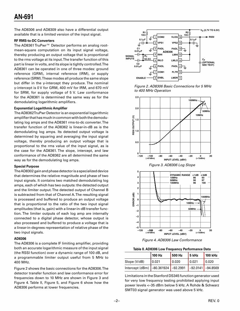
The AD8306 and AD8309 also have a differential output available that is a limited version of the input signal.
RF RMS-to-DC ConvertersThe AD8361 TruPwr™ Detector performs an analog root-mean-square computation on its input signal voltage, thereby producing an output voltage that is proportional to the rms voltage at its input. The transfer function of this part is linear in volts, and its slope is tightly controlled. The AD8361 can be operated in one of three modes: ground reference (GRM), internal reference (IRM), or supply reference (SRM). These modes all produce the same slope but differ in the y-intercept they produce. The nominal y-intercept is 0 V for GRM, 400 mV for IRM, and 670 mV for SRM, for supply voltage of 5 V. Law conformance for the AD8361 is determined the same way as for the demodulating logarithmic amplifiers.
Exponential Logarithmic AmplifierThe AD8362 TruPwr Detector is an exponential logarithmic amplifier that has much in common with both the demodu-lating log amps and the AD8361 rms-to-dc converter. The transfer function of the AD8362 is linear-in-dB as is the demodulating log amps. Its detected output voltage is determined by squaring and averaging the input signal voltage, thereby producing an output voltage that is proportional to the rms value of the input signal, as is the case for the AD8361. The slope, intercept, and law conformance of the AD8362 are all determined the same way as for the demodulating log amps.
Special PurposeThe AD8302 gain and phase detector is a specialized device that determines the relative magnitude and phase of two input signals. It contains two matched demodulating log amps, each of which has two outputs: the detected output and the limiter output. The detected output of Channel B is subtracted from that of Channel A. The resulting signal is processed and buffered to produce an output voltage that is proportional to the ratio of the two input signal amplitudes (that is, gain) with a linear-in-dB transfer func-tion. The limiter outputs of each log amp are internally connected to a digital phase detector, whose output is also processed and buffered to produce a voltage that is a linear-in-degrees representation of relative phase of the two input signals.
AD8306The AD8306 is a complete IF limiting amplifier, providing both an accurate logarithmic measure of the input signal (the RSSI function) over a dynamic range of 100 dB, and a programmable limiter output useful from 5 MHz to 400 MHz.
Figure 2 shows the basic connections for the AD8306. The detector transfer function and law conformance error for frequencies down to 10 MHz are shown in Figure 3 and Figure 4. Table II, Figure 5, and Figure 6 show how the AD8306 performs at lower frequencies.
�
�
�
�
�
�
�
�
����
����
����
����
����
����
����
����
����
����
����
����
����
����
����
����
������
�
��
��
��
��
�������
�����
���������
�����
������
�������
��������
������������
��
��
�����������������
��������
��������������������
Figure 2. AD8306 Basic Connections for 5 MHz to 400 MHz Operation
�����������������
���
����
������
���������
���
���
���
���
����� ��� ��� ��� ��� ���
�������� ��������
������
�����
�����
Figure 3. AD8306 Log Slope
�
����
����������
�
�
�
�
�
��
��
���� ��� ��� ��� ��� ��
��
��
������
�������������������������
���������
���������������������������������������������������������������������������������������������������������������������������������������������������������
������
�����
�����
Figure 4. AD8306 Law Conformance
Table II. AD8306 Low Frequency Performance Data
100 Hz 500 Hz 5 kHz 100 kHz
Slope (V/dB) 0.021 0.020 0.021 0.020
Intercept (dBm) –80.361924 –92.2991 –92.0141 –94.8569
Limitations in the Stanford DS345 function generator used for very low frequency testing prohibited applying input power levels <–35 dBm below 5 kHz. A Rohde & Schwarz SMT03 signal generator was used above 5 kHz.
REV. 0 REV. 0

–2–
AN-691
–3–
AN-691
�
����
����
����
����
����
����
����
����
����
�����
��
���
��
���������
��� ��� ��� ��� ��� ��� ��� ��� ��� � �� ��
�����
�����
������
����
Figure 5. AD8306 Detector Transfer Function for Low Frequencies
Despite the limitations with the test equipment, it was still possible to obtain detailed data about the AD8306’s ability to handle low frequency signals. To accomplish this, some modifications to the external circuitry of the device were necessary.
The minimum frequency that the AD8306 is capable of detecting is determined by the high-pass corner frequency of the matching network at the input pins INHI and INLO. The equation that describes this relationship is
fR CC
MIN =× ×
12π
where:
CC = C1 = C2 (see Figure 2).
The standard configuration of the evaluation board has R = 52.3 and CC = 0.01 F, setting the high-pass corner to be 304 kHz. Increasing CC to 10 F lowers the corner frequency to 304 Hz.
Figure 5 shows the log slope of the AD8306 at low frequen-cies. The specified slope and intercept are 20 mV/dB and –95 dBm, respectively. As the data in Table II and Figure 5 show, the AD8306 can perform very close to these data sheet specifications down to 500 Hz. Below 500 Hz, the part begins to experience significant change in intercept; however, the slope remains consistent. Law conformance (see Figure 6) also remains within the 1 dB specification, over the limited dynamic ranges.
����
����
����
����
�
���
��
��
���
��
�
���
���
���
��������� ������ ��� � �� ��
���������
����� �����
������
����
Figure 6. AD8306 Law Conformance for Low Frequencies
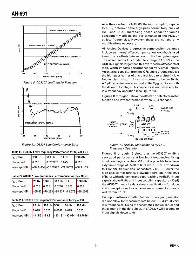
AD8307The AD8307 is a complete 500 MHz monolithic demodu-lating logarithmic amplifier based on the progressive compression technique, providing a dynamic range of 92 dB to 3 dB law conformance and 88 dB to a tight 1 dB error bound at all frequencies up to 100 MHz. It is extremely stable and easy to use, requiring no significant external components. A single-supply voltage of 2.7 V to 5.5 V at 7.5 mA is needed, corresponding to a power consumption of only 22.5 mW at 3 V. A fast acting, CMOS-compatible control pin can disable the AD8307 to a standby current of less than 150 A.
Figure 7, Figure 8, and Figure 9 show the basic connec-tions for using the log amp as well as the typical log slope and law conformance for various frequencies within the dynamic range specified in the data sheet.
��� ��� ��� ���
��� ��� ��� ���
������
�������
��������������������
����
�������
�������
����
��
��
������������������
��� ���
�������������
���������������
Figure 7. AD8307 Basic Connections
REV. 0 REV. 0
–4–
AN-691
–5–
AN-691
�����������������
�
���� �����
���������
��� ��� �
�
�
���������������������
����������������������
����������������������
����������������������
Figure 8. AD8307 Log Transfer Function
�����������������
�
�
����� �����
����������
��� ��� �
�
�
��
��
������������������������
������������������������
Figure 9. AD8307 Law Conformance Error
Table III. AD8307 Low Frequency Performance for CC = 0.1 F
PIN (dBm) 100 Hz 500 Hz 5 kHz 100 kHz
Slope (V/dB) 0.025 0.025337 0.025 0.025
Intercept (dBm) –38.94674 –52.01522 –71.88571 –88.34169
Table IV. AD8307 Low Frequency Performance for CC = 10 F
PIN (dBm) 20 Hz 100 Hz 500 Hz 5 kHz 100 kHz
Slope (V/dB) 0.025 0.025 0.0246 0.025 0.025
Intercept (dBm) –65.42 –79.293 –88.937 –89.673 –89.2263
Table V. AD8307 Low Frequency Performance for CC = 100 F
PIN (dBm) 20 Hz 100 Hz 500 Hz 5 kHz 100 kHz
Slope (V/dB) 0.025 0.025 0.0247 0.025 0.025
Intercept (dBm) –84.55 –89.9 –90.18 –90.034 –89.7626
As is the case for the AD8306, the input coupling capaci-tors, CC, determine the high-pass corner frequency at INHI and INLO. Increasing these capacitor values consequently affects the performance of the AD8307 at low frequencies. However, these are not the only modifications necessary.
All Analog Devices progressive compression log amps include an internal offset compensation loop that is used to null the dc offsets between each of the fixed gain stages. The offset feedback is limited to a range 1.5 mV in the AD8307. Signals larger than this override the offset control loop, which impacts performance for very small inputs. An external capacitor from the OFS pin to ground reduces the high-pass corner of this offset loop to arbitrarily low frequencies; using 1 F sets this corner to below 10 Hz. A 1 F capacitor was also used at the VOUT pin to smooth the dc output voltage. This capacitor is not necessary for low frequency operation (see Figure 10).
Figures 11 through 16 show the effects on detector transfer function and law conformance when CC is changed.
��� ��� ��� ���
��� ��� ��� ���
������
�������
��������������������
����
����������
�������
����
��
��� ���
������������������
��� ���
�������������
���������������
Figure 10. AD8307 Modifications for LowFrequency Operation
Figures 11 through 16 show that the AD8307 exhibits very good performance at low input frequencies. Using input coupling capacitors >10 F, it is possible to achieve a dynamic range of 55 dB to 60 dB with 1 dB error down to kilohertz frequencies. Capacitors >100 F lower the high-pass corner further, allowing operation in the 100s of hertz, with a dynamic range approaching 70 dB. For input signals above 5 kHz and input coupling capacitors >10 F, the AD8307 meets its data sheet specifications for slope and intercept as well as achieves measurement accuracy well within 1 dB.
It is important to note that limitations in the signal generator did not allow for measurements below –35 dBm at very low frequencies. Using the schematics shown earlier and those found in the data sheet, the AD8307 will respond to input signals down to dc.
REV. 0 REV. 0

–4–
AN-691
–5–
AN-691
�
����
����
����
����
����
����
����
����
����
����
����
��
����
��
���������
��� ��� ��� ��� ��� ��� ��� ��� ��� � �� ��
�����
�����
������
����
Figure 11. AD8307 Transfer Function for CC = 0.1 F
�
����
����
����
����
����
����
����
����
����
����
����
��
����
��
��� ��� ��� ��� ��� ��� ��� ��� � �� ��
���������
�����
����
�����������
����
Figure 12. AD8307 Transfer Function for CC = 10 F
�
����
����
����
����
����
����
����
����
����
����
����
��
����
��
��� ��� ��� ��� ��� ��� ��� ��� � �� ��
���������
�����
����
�����
������
����
Figure 13. AD8307 Transfer Function for CC = 100 F
����
����
����
����
�
���
��
��
���
��
�
���
���
���
��������� ������ ��� � �� ��
���������
���������������� ����
Figure 14. AD8307 Log Conformance Error for CC = 0.1 F
����
����
����
����
�
���
��
��
���
��
�
���
���
���
��������� ������ ��� �� � ��
���������
�����
���������
������
����
Figure 15. AD8307 Log Conformance Error for CC = 10 F
����
����
����
����
�
���
��
��
���
��
�
���
���
���
��� ��� ��� ��� ��� ��� ��� � �� ��
���������
�����
����
�����������
����
Figure 16. AD8307 Log Conformance Error for CC = 100 F
REV. 0 REV. 0

–6–
AN-691
–7–
AN-691
AD8309The AD8309 is a 500 MHz logarithmic amplifier based on the progressive compression (successive detection) technique. This log amp is useful for received signal strength indica-tion (RSSI) and phase detection in cellular base stations, radar, and other radio transceiver applications. It provides a dynamic range of 100 dB with an accuracy of 0.4 dB over the central 80 dB and operates at up to 500 MHz. The logarithmic output is proportional to the logarithm of the input signal, providing a 0.4 V to 2.5 V dc signal over the 100 dB input range. A limiter output that amplifies the input signal by 100 dB provides a stable, limited output with a maximum of 100 ps phase skew. This limiter output is useful for demodulating FSK- and PSK-modulated signals. The AD8309 operates from a single 2.7 V to 5.5 V dc power supply, typically drawing 20 mA.
�
�
�
�
�
�
�
�
����
����
����
����
����
����
����
����
����
����
����
����
����
����
����
����
������
�
��
��
��
��
�������
�����
�����
�����
������
����
����
����
�����
�����
������
��
��
��������������
�����
�����
������������������������������������ ���������������
��
��
��
Figure 17. AD8309 Basic Connections
������������������������
���
����
��
����
��
��
���
��
���
���
���
���
���� ��� ��� ��� �����
������������������
Figure 18. AD8309 Log Slope
������������������������
�
���
����������
�
�
�
�
�
��
��
��
��
����� ��� ��� ��� ��� ��� ��� ��� � �� �� ��
�������������������������������
�������������
����������
������
������
������
Figure 19. AD8309 Law Conformance
Performance of the AD8309 at low frequencies is very similar to that of the AD8306, the only difference being that the AD8306 is laser-trimmed to have less variation in slope and intercept.
The AD8309 meets data sheet specifications for slope and intercept down to 500 Hz. The part also exhibits a law conformance of 1 dB for approximately 60 dB by using input coupling capacitors of 10 F. Increasing the value of these capacitors to 100 F should increase the effective measurement range another 10 dB to 15 dB. This performance is indicated in Table VI and Figure 20 and Figure 21. More details can be found in the section about the AD8306.
Table VI. AD8309 Low Frequency Performance for CC = 10 F
PIN (dBm) 100 Hz 500 Hz 5 kHz 100 kHz
Slope (V/dB) 0.021 0.020 0.021 0.020
Intercept (dBm) –79.5967773 –91.25803 –91.09921 –93.77405
�
����
����
����
����
����
����
����
����
����
��
����
��
���������
��� ��� ��� ��� ��� ��� ��� ��� ��� � �� ��
�����
�����
������
����
Figure 20. AD8309 Transfer Function at Low Frequencies
REV. 0 REV. 0

–6–
AN-691
–7–
AN-691
����
����
����
����
�
���
��
��
���
��
�
���
���
���
��������� ������ ��� � �� ��
���������
�����
�����
������
����
Figure 21. AD8309 Law Conformance at Low Frequencies
AD8310The AD8310 is an ultrafast response, highly versatile logarithmic amplifier in an 8-lead MSOP package. It is a complete 400 MHz monolithic demodulating logarithmic amplifier based on the progressive compression technique, providing a dynamic range of 95 dB to 3 dB log conformance and 90 dB to a 1 dB error bound at frequencies up to 300 MHz. It is extremely stable and easy to use, requiring no significant external components. A single-supply voltage of 2.7 V to 5.5 V is required, resulting in a power dissipation of only 20 mW at 2.7 V. The AD8310 is an ideal choice for demanding IF signal measurement applications. The AD8310 has a very rapid 15 ns response time, enabling detection of ASK modulated waveforms to more than 10 MHz. Other applications include RSSI, transmit power control, and burst detection.
���������������
������
�����
���������������
��������
��������
��
��
���� ���� ���� ����
���� ���� ���� ����
������
������������
�����������
�����������
Figure 22. AD8310 Basic Connections
INPUT LEVEL (dBV)
3.0
–120 –100(–87dBm)
RS
SI O
UT
PU
T (
V)
–80 –60 –40 –20 0(+13dBm)
20
2.5
2.0
1.5
1.0
0.5
0
10MHz 50MHz
100MHz
Figure 23. AD8310 Log Slope
�����������������
�
������ ������
��������
��
��
���
��
�
��� ��� ��� ��� ���������
�
��
��
��
��
�
�
�
������
�����
������
Figure 24. AD8310 Law Conformance
Table VII. AD8310 Low Frequency Performance Data
PIN (dBm) 20 Hz 100 Hz 500 Hz 5 kHz 100 kHz
Slope (V/dB) 0.0249 0.02474 0.025 0.02481 0.02494
Intercept (dBm) –86.376 –92.0169 –91.517 –92.277 –91.769
The AD8310 performs extremely well at low frequencies. As with the other progressive compression log amps, it is necessary to increase the input coupling capacitors to lower the high-pass corner at INHI and INLO. For low frequency applications, this value should be 10 F.
Like the AD8307, the AD8310’s offset compensation loop must be adjusted. With no external compensation, the corner frequency of the loop is 2 MHz. Connecting a 1 F capacitor to the OFLT pin reduces the low-pass corner so that it has a 3 dB frequency at 60 Hz.
It is also necessary to use some filtering to reduce mea-surement noise. Implementing a 2.7 nF capacitor on BFIN reduces the bandwidth of the output stage and increases the accuracy of the output log voltage. Figure 27 shows these modifications.
Figure 25 and Figure 26 show the log slope and accuracy of the AD8310 when operating at low frequencies. Slope and
REV. 0 REV. 0

–8–
AN-691
–9–
AN-691
intercept remain within data sheet specifications down to 100 Hz. The intercept begins to drift up as the input signal drops below 100 Hz, but the slope remains constant.
�
���
���
���
���
���
���
��
����
��
���� ��� ��� ��� ��� ��� ��� ��� ��� ��� � �� ��
���������
�����
����
�����
������
����
Figure 25. AD8310 Log Slope at Low Frequencies
����
����
����
����
�
���
��
��
���
��
�
���
���
���
��� ��� ��� ��� ��� ��� ��� ��� � �� ��
���������
�����
���������������
����
Figure 26. AD8310 Law Conformance at Low Frequencies
�������������
�����
�������
���
�
���� ���� ���� ����
���� ���� ���� ����
������
������������
�����������
�����������
�������
��
Figure 27. AD8310 Modifications for Low Frequency Operation
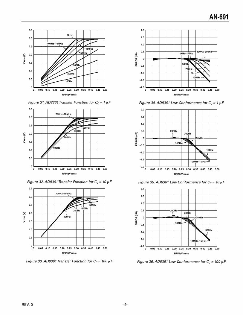
AD8361The AD8361 is a TruPwr Detection RFIC, offering for the first time RF rms responding power detection in integrated form. This device can convert a complex modulated RF signal up to 2.5 GHz into a dc voltage representing the
rms level of the RF signal. It is highly linear, temperature stable, and is useful for detecting CDMA, QAM, and other complex modulation schemes. The dynamic range is 30 dB. Measurement accuracy is 0.25 dB over the top 14 dB of the dynamic range and 1 dB over the top 23 dB range. The AD8361 is offered in a small 8-lead MSOP package and requires only 1.1 mA from a 2.7 V to 5.5 V power supply.
����������
����
����
����
����
����
����
����
�
�
�
�
�
�
�
�
�����
�����
������
�����
���������������
����
�������
Figure 28. AD8361 Basic Connections
�������������
���
���
���
� ��� ��� ��� ��� ���
���
���
���
���
���
���
���
���
��
��
��
���
�
���
���
���
�
������
�������������
������
Figure 29. AD8361 Slope at Various Frequen-cies, GND Reference Mode, 2.7 V Supply
�������������
���
���
����
����������
����
���
�
����
���
���
���
��
��
���
��
�
����
����
����
�������
�����������
��������
�������������
Figure 30. AD8361 Error at 900 MHz, GND Reference Mode, 2.7 V Supply
REV. 0 REV. 0
–8–
AN-691
–9–
AN-691
�
���
���
���
���
���
���
���
���
���
���
� ���� ���� ���� ���� ���� ���� ���� ���� ���� ����
������������
�����
�����
�����
�����
�����
�����������
����
Figure 31. AD8361 Transfer Function for CC = 1 F
�
���
���
���
���
���
���
���
���
���
���
� ���� ���� ���� ���� ���� ���� ���� ���� ���� ����
������������
�����
�����
�����
�����
�����������
Figure 32. AD8361 Transfer Function for CC = 10 F
�
���
���
���
���
���
���
���
���
���
���
� ���� ���� ���� ���� ���� ���� ���� ���� ���� ����
������������
�����
�����
�����
�����
�����������
Figure 33. AD8361 Transfer Function for CC = 100 F
����
����
����
����
�
���
��
��
���
��
�
���
���
���
� ���� ���� ���� ���� ���� ���� ���� ���� ���� ����
������������
�����������
����
�����
�����
�����
����������
Figure 34. AD8361 Law Conformance for CC = 1 F
����
����
����
����
�
���
��
��
���
��
�
���
���
���
� ���� ���� ���� ���� ���� ���� ���� ���� ���� ����
������������
�����
�����
����������
�����
�����
������
Figure 35. AD8361 Law Conformance for CC = 10 F
����
����
����
����
�
���
��
��
���
��
�
���
���
���
� ���� ���� ���� ���� ���� ���� ���� ���� ���� ����
������������
�����
�����
����������
�����
�����
������
Figure 36. AD8361 Law Conformance for CC = 100 F
REV. 0 REV. 0

–10–
AN-691
–11–
AN-691
The AD8361 has three different reference modes of opera-tion. The device used to collect the data for this application note was set to ground reference mode (GRM). In this mode, the output of the AD8361 ideally is 0 V for no input signal. Each part exhibits some small offset voltage, typically a few 10s of millivolts.
Much like the demodulating log amps, the AD8361’s input sits at a bias potential above ground. For this reason, an ac-coupling capacitor is necessary. The combination of the 225 input impedance and series capacitor, CC, form a high-pass filter that determines the lowest frequency that the device can measure. This is the only part of the circuit that is modified to allow the AD8361 to measure low frequency signals. It is advisable to use an external capacitor on the FLTR pin to reduce noise on the output signal, but this is not required.
The data in Tables VIII, IX, and X, and the previous plots reflect the dependency on the input capacitor, CC. The 3 dB cutoff of this filter is given by
fC RC IN
31
2dB =π × ×
Using a filter capacitor of 1 F sets the high-pass corner to 700 Hz, allowing the AD8361 to perform consistently to data sheet specifications down to 10 kHz. It is interesting to note that the part did respond to signals as low as 100 Hz. Although the slope was much lower, the intercept remained very close to zero and a linear response was observed. Increasing CC to 10 F lowers the high-pass corner to 70 Hz. The AD8361 now begins to match the expected slope and intercept specifications at 700 Hz. Using 100 F, the response of the part is nearly
indistinguishable for frequencies above 100 Hz with input signals less than 0.2 V rms. The response is affected only at the higher input signal levels.
Error of this device is extremely good despite reduced slope response for smaller values of CC. The previous plots show that this error never exceeds –2 dB.
AD8362The AD8362, the next generation TruPwr Detector, is designed to provide wide dynamic range signal level measurement to 60 dB within wireless infrastructure equipment. The product provides an accurately scaled linear-in-dB output response that is the equivalent root-mean-square (rms) of the input waveform, making this detector ideally suited for the measurement of complex modulated waveforms with large crest factors. Effectively modulation-independent, the AD8362 is ideal for use in high data rate wireless networks that use WCDMA, QAM/QPSK, or OFDM modulation.
��
��
��
��
��
��
��
�
�
�
�
�
�
�
�
�
����
����
����
����
����
����
����
����
����
����
����
����
����
����
����
����
���
����
������
������������������������������������
������������������������
����
����
����������������
�����
����
����
����
����
Figure 37. AD8362 Typical Connections for Measurement Mode
Table VIII. AD8361 Low Frequency Performance for CC = 1 F
Frequency
PIN (dBm) 100 Hz 200 Hz 300 Hz 500 Hz 700 Hz 1 kHz 10 kHz 100 kHz 1 MHz 10 MHz
Slope (V/V) 2.076429 3.684286 4.990714 6.898857 7.766286 8.233714 10.032 9.974 10.242 10.242
Intercept (dBm) –0.002328 –0.01208 –0.01261 –0.00858 –0.01139 –0.016 –0.00242 –0.00262 –0.00153 –0.00153
Table IX. AD8361 Low Frequency Performance for CC = 10 F
Frequency
PIN (dBm) 100 Hz 200 Hz 300 Hz 500 Hz 700 Hz 1 kHz 10 kHz 100 kHz 1 MHz 10 MHz
Slope (V/) 8.64 9.67 9.86 9.98 10.01 10.03 10.01 10.04 10.07 10.13
Intercept (dBm) –0.00601 –0.00309 –0.00371 –0.00356 –0.00357 –0.00356 –0.00363 –0.00252 –0.00341 –0.0032
Table X. AD8361 Low Frequency Performance for CC = 100 F
Frequency
PIN (dBm) 100 Hz 200 Hz 300 Hz 500 Hz 700 Hz 1 kHz 10 kHz 100 kHz 1 MHz 10 MHz
Slope (V/V) 10.06 10.10 10.07 10.06 10.06 10.05 10.01 9.95 10.06 10.13
Intercept (dBm) –0.00206 –0.00259 –0.00322 –0.0034 –0.00344 –0.00362 –0.00373 –0.00366 –0.0036 –0.0032
REV. 0 REV. 0

–10–
AN-691
–11–
AN-691
Table XI. AD8362 Slope and Error Data for CC = 0.1 F
PIN (dBm) 10 kHz 100 kHz
Slope (V/dB) 0.013 0.013
Intercept (dBm) –49.9337406 –49.90699
Table XII. AD8362 Slope and Error Data for CC = 10 F
PIN (dBm) 20 Hz 100 Hz 500 Hz 5 kHz 100 kHz
Slope (V/dB) 0.025 0.025 0.0246 0.025 0.025
Intercept (dBm) –65.42 –79.293 –88.937 –89.673 –89.2263
Table XIII. AD8362 Slope and Error Data for CC = 100 F
PIN (dBm) 20 Hz 100 Hz 500 Hz 5 kHz 100 kHz
Slope (V/dB) 0.025 0.025 0.0247 0.025 0.025
Intercept (dBm) –84.55 –89.9 –90.18 –90.034 –89.7626
���������������������
����
��
����
��
���
��� ��� ��� ��� ��� ��� ��� ��� ��� �� � � ��
���
���
���
���
���
���
���
���
��
������
������
�������
���
�������
�������
Figure 38. AD8362 Log Slope for Various Frequencies
���������������������
�������
��������
����������
����
��� ��� ��� ��� ��� ��� ��� ��� ��� �� � � ��
����
����
���
���
���
���
���
����
��
������
�������
�������
�������
����
���
������
���
�
Figure 39. AD8362 Law Conformance for Various Frequencies
The AD8362 is comprised of an AGC loop. The RF input to the loop drives a VGA, which is composed of a variable attenuator driving a fixed-gain amplifier. The amplifier’s output is squared; the squared signal is then integrated by an internal shunt capacitor, which in most applications is augmented by an external shunt capacitor. This squared, averaged signal is then compared to a nominally static reference signal. The result of this comparison drives the attenuation control of the input VGA. This voltage, available at Pin VOUT, is proportional to the common logarithm of the input signal rms voltage.
The bandwidth of the VGA in the AD8362 is independent of its gain. Because this amplifier is internally dc-coupled, the system can be used as an accurate rms voltmeter, retaining its temperature-stable decibel-scaled output, down to arbitrarily low frequencies, for example, in seismic, audio, or sonar instrumentation. This is in contrast to some rms-to-dc converter architectures, most of which have full bandwidth only at full-scale input, and reduced bandwidth as input level decreases.
The input coupling capacitors for the AD8362 should be large enough that the lowest frequency components of the signal, which are to be included in the measurement, are minimally attenuated. For example, for a 3 dB reduction at 1.5 kHz, capacitances of 1 F are needed because the input resistance is 100 V at each input pin, (200 V differentially) and 1/(2 1500 100) = 1 F. Also, to lower the high-pass corner frequency of the VGA, a 50 F-Hz capacitor should be used between the CHPF pin and ground; to provide a similar 1.5 kHz high-pass corner, a 33 nF capacitor should be used.
The external low-pass averaging capacitance, CLPF, added at the output of the squaring cell, should be chosen to provide adequate filtering of the detected signal, as well as to maintain the stability of the AGC loop. The optimum value depends on the application, but as a guideline a value of the order of 900 F-Hz should be used. For example, a capacitance of 5 F provides adequate filtering down to 180 Hz.
REV. 0 REV. 0

–12–
AN-691
–13–
AN-691
�
���
���
���
���
���
���
���
��
����
��
��� ��� ��� ��� ��� ��� � ��
���������
������
�����
Figure 40. AD8362 Transfer Function for CC = 0.1 F
�
����
����
����
����
����
����
����
����
����
����
����
��
����
��
��� ��� ��� ��� ��� ��� ��� ��� � �� ��
���������
�����
����
�����
������
����
Figure 41. AD8362 Transfer Function for CC = 10 F
�
����
����
����
����
����
����
����
����
����
����
����
��
����
��
��� ��� ��� ��� ��� ��� ��� ��� � �� ��
���������
�����
����
�����
������
����
Figure 42. AD8362 Transfer Function for CC = 100 F
����
����
����
����
�
���
��
��
���
��
�
���
���
���
��� ��� ��� ��� ��� ��� � ��
���������
������
�����
Figure 43. AD8362 Law Conformance for CC = 0.1 F
����
����
����
����
�
����
��
��
���
��
���
���
���
��������� ������ ��� �� � ��
���������
�����
����
�����
������
����
Figure 44. AD8362 Law Conformance for CC = 10 F
����
����
����
����
�
���
��
��
���
��
�
���
���
���
��� ��� ��� ��� ��� ��� ��� � �� ��
���������
�����
���������
������
����
Figure 45. AD8362 Law Conformance for CC = 100 F
REV. 0 REV. 0

–12–
AN-691
–13–
AN-691
AD8302The AD8302 is a fully integrated RF IC that measures the relative amplitude and phase of two independent input signals. The device is characterized in the AD8302 data sheet for use over the common cellular bands (900 MHz, 1.8 GHz, and 2.2 GHz) and can be used from low frequencies up to 2.7 GHz. The AD8302 integrates two closely matched wideband demodulating logarithmic amplifiers, a wideband digital phase detector, a precision 1.8 V reference, and analog output scaling circuits. The applied input signals can range from –60 dBm to 0 dBm (re: 50 ), corresponding to a 60 dB dynamic range. The output provides an accurate amplitude measurement over 30 dB range scaled to 30 mV/dB and the phase measurement over a 0 to 180 range scaled to 10 mV/degree.
�
�
�
�
�
�
�
���� ���� ��
���� ���� ��
���� ���� ��
���� ���� ��
���� ���� ��
�
�
���� ����
���� ����
������
������
����
��
��
��
��
��
��
��
����
����
��
��
��
��
Figure 46. AD8302 Basic Connections
�����������������������
��
��
���
�
����
���� ��� � �� �� ��
���
��
��
����
���
��
���
��
���
���
���
���
���
�
����
����
����
����
����
����
����
����
����
����
����
����
����
����
����
����
����
�����
�����
�����
Figure 47. AD8302 Log Slope and Error at 100 MHz
PHASE DIFFERENCE (Degrees)
PH
AS
E O
UT
(V
)
–180 –150
1.80
–120 –90 –60 –30 0 30 60 90
1.62
1.44
1.26
1.08
0.90
0.72
0.54
0.36
0.00120 150 180
0.18
ER
RO
R (
Deg
rees
)
10
8
6
4
2
0
–2
–4
–6
–10
–8
Figure 48. AD8302 Phase Output and Nonlinearity
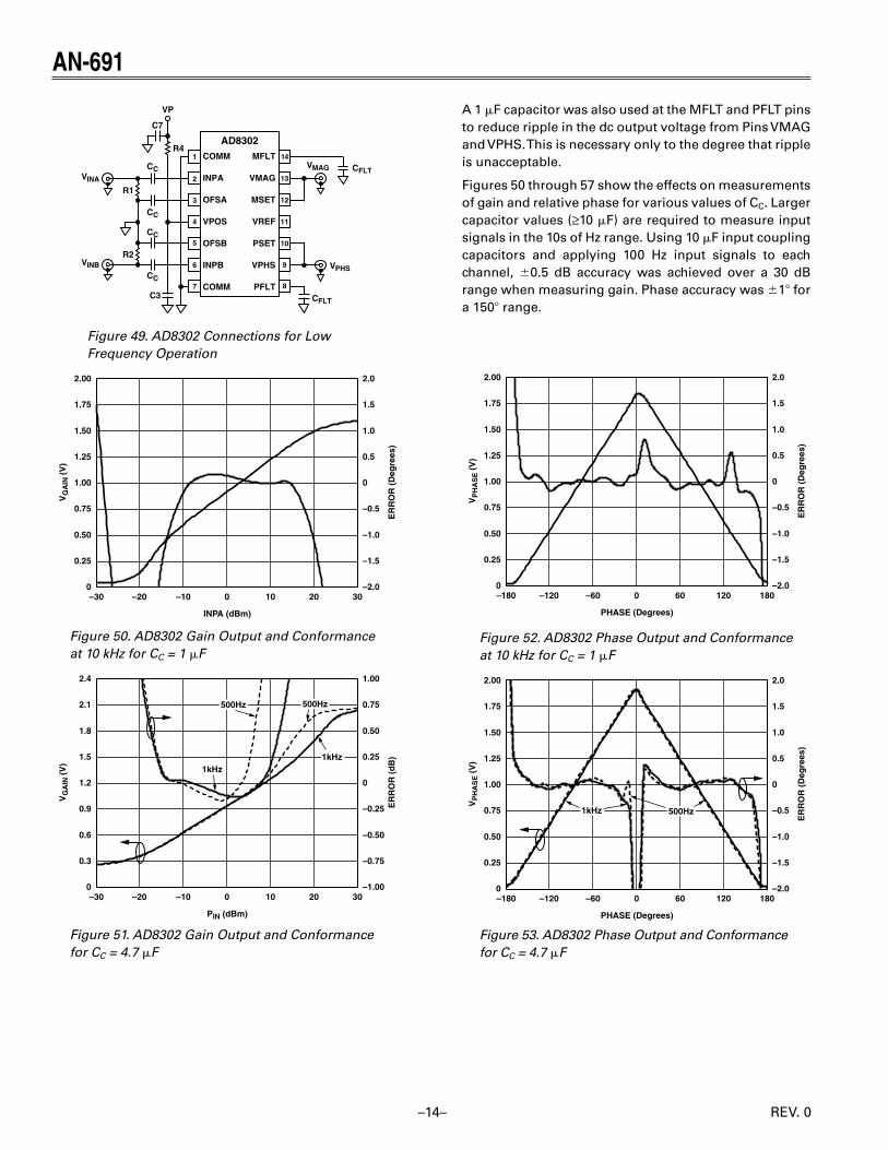
The modification of the input circuitry for the AD8302 to operate at low frequencies is similar to that required for the single-channel log amps. Figure 49 shows the modification necessary for low frequency operation.
The input coupling capacitors, CC, determine the high-pass corner frequency at INPA and OFSA, as do their counterparts in the second log channel, INPB and OFSB. Increasing these capacitor values enables improved performance of the AD8302 at low frequencies.
Table XIV. AD8302 Gain – CC = 10 F, CFLT = 1 F
VMAG
PIN (dBm) 20 Hz 100 Hz 500 Hz 1 kHz
Slope (v/dB) 0.03072 0.029585714 0.02964 0.029603333
Intercept (dBm) –30.82379955 –31.51145534 –31.50641271 –31.5572116
Table XV. AD8302 Phase – CC = 10 F, CFLT = 1 F
VPHS
PIN (dBm) 20 Hz 100 Hz 500 Hz 1 kHz
P_Slope 0.011031515 0.011037576 0.011032121 0.011036813
N_Slope –0.010994545 –0.011036813 –0.011024545 –0.01104
PS_Intercept –171.4731041 –174.7615324 –169.96435 –174.3398531
NS_Intercept 177.664949 173.4617513 178.4263471 173.9210955
REV. 0 REV. 0
–14–
AN-691
–15–
AN-691
�
�
�
�
�
�
�
���� ���� ��
���� ���� ��
���� ���� ��
���� ���� ��
���� ���� ��
�
�
���� ����
���� ����
������
��������
����
����
��
��
��
��
��
��
����
����
��
��
��
��
Figure 49. AD8302 Connections for Low Frequency Operation
0
0.25
0.50
0.75
1.00
1.25
VG
AIN
(V
)
1.50
1.75
2.00
–2.0
–1.5
–1.0
–0.5
0
0.5
ER
RO
R (
Deg
rees
)
1.0
1.5
2.0
–10 0–30 –20 10 20 30
INPA (dBm)
Figure 50. AD8302 Gain Output and Conformance at 10 kHz for CC = 1 F
�
���
���
���
���
���
��
���
���
�
���
���
���
�����
�����
�����
�����
�
����
��
��
���
��
�
����
����
����
��� ���� ��� �� �� ��
���������
��������
����������
Figure 51. AD8302 Gain Output and Conformance for CC = 4.7 F
A 1 F capacitor was also used at the MFLT and PFLT pins to reduce ripple in the dc output voltage from Pins VMAG and VPHS. This is necessary only to the degree that ripple is unacceptable.
Figures 50 through 57 show the effects on measurements of gain and relative phase for various values of CC. Larger capacitor values (≥10 F) are required to measure input signals in the 10s of Hz range. Using 10 F input coupling capacitors and applying 100 Hz input signals to each channel, 0.5 dB accuracy was achieved over a 30 dB range when measuring gain. Phase accuracy was 1 for a 150 range.
0
0.25
0.50
0.75
1.00
1.25
VP
HA
SE (
V)
1.50
1.75
2.00
–2.0
–1.5
–1.0
–0.5
0
0.5
ER
RO
R (
Deg
rees
)
1.0
1.5
2.0
–60 0–180 –120 60 120 180
PHASE (Degrees)
Figure 52. AD8302 Phase Output and Conformance at 10 kHz for CC = 1 F
�
����
����
����
����
����
��
��
����
��
����
����
����
����
����
����
����
�
���
��
��
���
���
����
�
���
���
���
��� ����� ���� �� ��� ���
���������������
���� �����
Figure 53. AD8302 Phase Output and Conformancefor CC = 4.7 F
REV. 0 REV. 0

–14–
AN-691
–15–
AN-691
�
���
���
���
���
���
���
��
���
���
�
���
���
���
��� ���� ��� �� �� ��
���������
�����
��������
�����
Figure 54. AD8302 Gain Output for CC = 100 F
�
����
����
����
����
����
��
��
����
��
����
����
����
��� ����� ���� �� ��� ���
���������������
�����
����
����
�����
Figure 55. AD8302 Phase Output for CC = 100 F
����
����
����
����
�
���
���
���
��
��
���
��
�
��� ���� ��� �� �� ��
���������
�����
����
����
�����
Figure 56. AD8302 Gain Conformance for CC = 100 F
��
��
��
�
�
�
�
��
��
���
���
����
�
��� ����� ���� �� ��� ���
���������������
�����
���� ����
�����
Figure 57. AD8302 Phase Conformance for CC = 100 F
CONCLUSIONADI’s high frequency demodulating logarithmic amplifiers (AD8306, AD8307, AD8309, and AD8310), RF rms-to-dc TruPwr Detector (AD8361), exponential AGC RF TruPwr Detector (AD8362), and RF gain and phase detector (AD8302) provide excellent performance at high input signal frequencies and are shown to operate accurately at sub-RF input signal frequencies as well, in some cases to the low end of the audio spectrum.
REV. 0 REV. 0

AN
0456
2–0–
5/05
(0)
–16–© 2005 Analog Devices, Inc. All rights reserved. Trademarks and registered trademarks are the property of their respective owners.