AMAT =HitTime MissRate ×MissPenalt y
19
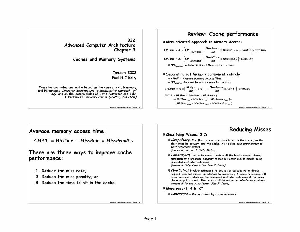
Page 1 Advanced Computer Architecture Chapter 3.1 332 Advanced Computer Architecture Chapter 3 Caches and Memory Systems January 2003 Paul H J Kelly These lecture notes are partly based on the course text, Hennessy and Patterson’s Computer Architecture, a quantitative approach (3 rd ed), and on the lecture slides of David Patterson and John Kubiatowicz’s Berkeley course (CS252, Jan 2001) Advanced Computer Architecture Chapter 3.2 Miss-oriented Approach to Memory Access: CPI Execution includes ALU and Memory instructions CycleTime y MissPenalt MissRate Inst MemAccess Execution CPI IC CPUtime × ⎟ ⎠ ⎞ ⎜ ⎝ ⎛ × × + × = CycleTime y MissPenalt Inst MemMisses Execution CPI IC CPUtime × ⎟ ⎠ ⎞ ⎜ ⎝ ⎛ × + × = Review: Cache performance Separating out Memory component entirely AMAT = Average Memory Access Time CPI ALUOps does not include memory instructions CycleTime AMAT Inst MemAccess CPI Inst AluOps IC CPUtime AluOps × ⎟ ⎠ ⎞ ⎜ ⎝ ⎛ × + × × = y MissPenalt MissRate HitTime AMAT × + = ( ) ( ) Data Data Data Inst Inst Inst y MissPenalt MissRate HitTime y MissPenalt MissRate HitTime × + + × + = Advanced Computer Architecture Chapter 3.3 There are three ways to improve cache performance: 1. Reduce the miss rate, 2. Reduce the miss penalty, or 3. Reduce the time to hit in the cache. y MissPenalt MissRate HitTime AMAT × + = Average memory access time: Advanced Computer Architecture Chapter 3.4 Reducing Misses Classifying Misses: 3 Cs Compulsory—The first access to a block is not in the cache, so the block must be brought into the cache. Also called cold start misses or first reference misses. (Misses in even an Infinite Cache) Capacity—If the cache cannot contain all the blocks needed during execution of a program, capacity misses will occur due to blocks being discarded and later retrieved. (Misses in Fully Associative Size X Cache) Conflict—If block-placement strategy is set associative or direct mapped, conflict misses (in addition to compulsory & capacity misses) will occur because a block can be discarded and later retrieved if too many blocks map to its set. Also called collision misses or interference misses. (Misses in N-way Associative, Size X Cache) More recent, 4th “C”: Coherence - Misses caused by cache coherence.
Transcript of AMAT =HitTime MissRate ×MissPenalt y
Page 1
Advanced Computer Architecture Chapter 3.1
332Advanced Computer Architecture
Chapter 3
Caches and Memory Systems
January 2003Paul H J Kelly
These lecture notes are partly based on the course text, Hennessy and Patterson’s Computer Architecture, a quantitative approach (3rd
ed), and on the lecture slides of David Patterson and John Kubiatowicz’s Berkeley course (CS252, Jan 2001)
Advanced Computer Architecture Chapter 3.2
Miss-oriented Approach to Memory Access:
CPIExecution includes ALU and Memory instructions
CycleTimeyMissPenaltMissRateInst
MemAccessExecution
CPIICCPUtime ×⎟⎠⎞
⎜⎝⎛ ××+×=
CycleTimeyMissPenaltInst
MemMissesExecution
CPIICCPUtime ×⎟⎠⎞
⎜⎝⎛ ×+×=
Review: Cache performance
Separating out Memory component entirelyAMAT = Average Memory Access TimeCPIALUOps does not include memory instructions
CycleTimeAMATInst
MemAccessCPIInst
AluOpsICCPUtime AluOps ×⎟⎠⎞
⎜⎝⎛ ×+××=
yMissPenaltMissRateHitTimeAMAT ×+=( )( )DataDataData
InstInstInst
yMissPenaltMissRateHitTimeyMissPenaltMissRateHitTime
×+
+×+=
Advanced Computer Architecture Chapter 3.3
There are three ways to improve cache performance:
1. Reduce the miss rate, 2. Reduce the miss penalty, or3. Reduce the time to hit in the cache.
yMissPenaltMissRateHitTimeAMAT ×+=
Average memory access time:
Advanced Computer Architecture Chapter 3.4
Reducing MissesClassifying Misses: 3 Cs
Compulsory—The first access to a block is not in the cache, so the block must be brought into the cache. Also called cold start misses or first reference misses.(Misses in even an Infinite Cache)
Capacity—If the cache cannot contain all the blocks needed during execution of a program, capacity misses will occur due to blocks being discarded and later retrieved.(Misses in Fully Associative Size X Cache)
Conflict—If block-placement strategy is set associative or direct mapped, conflict misses (in addition to compulsory & capacity misses) will occur because a block can be discarded and later retrieved if too many blocks map to its set. Also called collision misses or interference misses.(Misses in N-way Associative, Size X Cache)
More recent, 4th “C”:Coherence - Misses caused by cache coherence.
Page 2
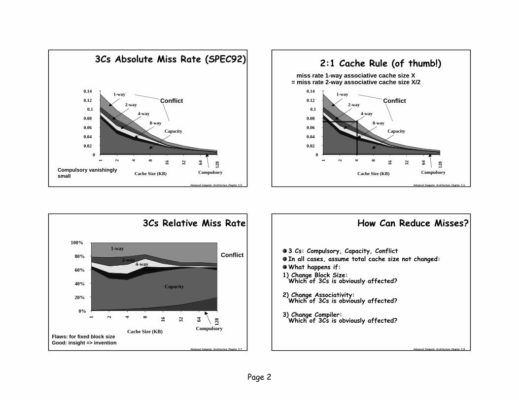
Advanced Computer Architecture Chapter 3.5
Cache Size (KB)
0
0.02
0.04
0.06
0.08
0.1
0.12
0.14
1 2 4 8
16 32 64
128
1-way
2-way
4-way
8-way
Capacity
Compulsory
3Cs Absolute Miss Rate (SPEC92)
Conflict
Compulsory vanishinglysmall
Advanced Computer Architecture Chapter 3.6
Cache Size (KB)
0
0.02
0.04
0.06
0.08
0.1
0.12
0.14
1 2 4 8
16 32 64
128
1-way
2-way
4-way
8-way
Capacity
Compulsory
2:1 Cache Rule (of thumb!)
Conflict
miss rate 1-way associative cache size X = miss rate 2-way associative cache size X/2
Advanced Computer Architecture Chapter 3.7
3Cs Relative Miss Rate
Cache Size (KB)
0%
20%
40%
60%
80%
100%
1 2 4 8
16 32 64
128
1-way
2-way4-way
8-way
Capacity
Compulsory
Conflict
Flaws: for fixed block sizeGood: insight => invention
Advanced Computer Architecture Chapter 3.8
How Can Reduce Misses?
3 Cs: Compulsory, Capacity, ConflictIn all cases, assume total cache size not changed:What happens if:
1) Change Block Size: Which of 3Cs is obviously affected?
2) Change Associativity: Which of 3Cs is obviously affected?
3) Change Compiler: Which of 3Cs is obviously affected?

Page 3
Advanced Computer Architecture Chapter 3.9
Block Size (bytes)
Miss Rate
0%
5%
10%
15%
20%
25%
16 32 64
128
256
1K
4K
16K
64K
256K
1. Reduce Misses via Larger Block Size
Advanced Computer Architecture Chapter 3.10
2. Reduce Misses via Higher Associativity
2:1 Cache Rule of thumb: The Miss Rate of a direct-mapped cache of size N Is the same as the Miss Rate of a 2-way set-associative cache size of size N/2
on average, over a large suite of benchmarks
Beware: Execution time is only final measure!Will Clock Cycle time increase?Hill [1988] suggested hit time for 2-way vs. 1-way external cache +10%, internal + 2%
Advanced Computer Architecture Chapter 3.11
Example: Avg. Memory Access Time vs. Miss Rate
Example: assume CCT = 1.10 for 2-way, 1.12 for 4-way, 1.14 for 8-way vs. CCT direct mapped
Cache Size Associativity(KB) 1-way 2-way 4-way 8-way1 2.33 2.15 2.07 2.012 1.98 1.86 1.76 1.684 1.72 1.67 1.61 1.538 1.46 1.48 1.47 1.4316 1.29 1.32 1.32 1.3232 1.20 1.24 1.25 1.2764 1.14 1.20 1.21 1.23128 1.10 1.17 1.18 1.20
(Red means A.M.A.T. not improved by more associativity)
Advanced Computer Architecture Chapter 3.12
3. Reducing Misses via a“Victim Cache”
How to combine fast hit time of direct mapped yet still avoid conflict misses? Add buffer to place data discarded from cacheJouppi [1990]: 4-entry victim cache removed 20% to 95% of conflicts for a 4 KB direct mapped data cacheUsed in Alpha, HP machines
To Next Lower Level InHierarchy
DATATAGS
One Cache line of DataTag and Comparator
One Cache line of DataTag and Comparator
One Cache line of DataTag and Comparator
One Cache line of DataTag and Comparator

Page 4
Advanced Computer Architecture Chapter 3.13
4. Reducing Misses via “Pseudo-Associativity”
How to combine fast hit time of Direct Mapped and have the lower conflict misses of 2-way SA cache? Divide cache: on a miss, check other half of cache to see if there, if so have a pseudo-hit (slow hit)
Drawback: CPU pipeline is hard if hit takes 1 or 2 cyclesBetter for caches not tied directly to processor (L2)Used in MIPS R10000 L2 cache, similar in UltraSPARC
Hit Time
Pseudo Hit Time Miss Penalty
Time
Advanced Computer Architecture Chapter 3.14
5. Reducing Misses by HardwarePrefetching of Instructions & Data
E.g., Instruction PrefetchingAlpha 21064 fetches 2 blocks on a missExtra block placed in “stream buffer”On miss check stream buffer
Works with data blocks too:Jouppi [1990] 1 data stream buffer got 25% misses from 4KB cache; 4 streams got 43%Palacharla & Kessler [1994] for scientific programs for 8 streams got 50% to 70% of misses from 2 64KB, 4-way set associative caches
Prefetching relies on having extra memory bandwidth that can be used without penalty
Advanced Computer Architecture Chapter 3.15
6. Reducing Misses by Software Prefetching Data
Data PrefetchLoad data into register (HP PA-RISC loads)Cache Prefetch: load into cache (MIPS IV, PowerPC, SPARC v. 9)Special prefetching instructions cannot cause faults; a form of speculative execution
Prefetching comes in two flavors:Binding prefetch: Requests load directly into register.
Must be correct address and register!Non-Binding prefetch: Load into cache.
Can be incorrect. Frees HW/SW to guess!Issuing Prefetch Instructions takes time
Is cost of prefetch issues < savings in reduced misses?Higher superscalar reduces difficulty of issue bandwidth
Advanced Computer Architecture Chapter 3.16
7. Reducing Misses by Compiler Optimizations
McFarling [1989] reduced caches misses by 75% on 8KB direct mapped cache, 4 byte blocks in softwareInstructions
Reorder procedures in memory so as to reduce conflict missesProfiling to look at conflicts(using tools they developed)
DataMerging Arrays: improve spatial locality by single array of compound elements vs. 2 arraysLoop Interchange: change nesting of loops to access data in order stored in memoryLoop Fusion: Combine 2 independent loops that have same looping and some variables overlapBlocking: Improve temporal locality by accessing “blocks” of data repeatedly vs. going down whole columns or rows

Page 5
Advanced Computer Architecture Chapter 3.17
Merging Arrays Example
/* Before: 2 sequential arrays */int val[SIZE];int key[SIZE];
/* After: 1 array of stuctures */struct merge {
int val;int key;
};struct merge merged_array[SIZE];
Reducing conflicts between val & key; improve spatial locality
Advanced Computer Architecture Chapter 3.18
Loop Interchange Example
/* Before */for (k = 0; k < 100; k = k+1)
for (j = 0; j < 100; j = j+1)for (i = 0; i < 5000; i = i+1)
x[i][j] = 2 * x[i][j];/* After */for (k = 0; k < 100; k = k+1)
for (i = 0; i < 5000; i = i+1)for (j = 0; j < 100; j = j+1)
x[i][j] = 2 * x[i][j];
Sequential accesses instead of striding through memory every 100 words; improved spatial locality
Advanced Computer Architecture Chapter 3.19
Loop Fusion Example/* Before */for (i = 0; i < N; i = i+1)
for (j = 0; j < N; j = j+1)a[i][j] = 1/b[i][j] * c[i][j];
for (i = 0; i < N; i = i+1)for (j = 0; j < N; j = j+1)
d[i][j] = a[i][j] + c[i][j];/* After */for (i = 0; i < N; i = i+1)
for (j = 0; j < N; j = j+1){ a[i][j] = 1/b[i][j] * c[i][j];
d[i][j] = a[i][j] + c[i][j];}
2 misses per access to a & c vs. one miss per access; improve spatial locality
Advanced Computer Architecture Chapter 3.20
Blocking Example/* Before */for (i = 0; i < N; i = i+1)
for (j = 0; j < N; j = j+1){r = 0;for (k = 0; k < N; k = k+1){r = r + y[i][k]*z[k][j];};
x[i][j] = r;};
Two Inner Loops:Read all NxN elements of z[]Read N elements of 1 row of y[] repeatedlyWrite N elements of 1 row of x[]
Capacity Misses a function of N & Cache Size:2N3 + N2 => (assuming no conflict; otherwise …)
Idea: compute on BxB submatrix that fits

Page 6
Advanced Computer Architecture Chapter 3.21
Blocking Example/* After */for (jj = 0; jj < N; jj = jj+B)for (kk = 0; kk < N; kk = kk+B)for (i = 0; i < N; i = i+1)
for (j = jj; j < min(jj+B-1,N); j = j+1){r = 0;for (k = kk; k < min(kk+B-1,N); k = k+1) {r = r + y[i][k]*z[k][j];};
x[i][j] = x[i][j] + r;};
B called Blocking FactorCapacity Misses from 2N3 + N2 to N3/B+2N2
Conflict Misses Too?
Advanced Computer Architecture Chapter 3.22
Reducing Conflict Misses by Blocking
Conflict misses in caches not FA vs. Blocking sizeLam et al [1991] a blocking factor of 24 had a fifth the misses vs. 48 despite both fit in cache
Blocking Factor
0
0.05
0.1
0 50 100 150
Fully Associative Cache
Direct Mapped Cache
Advanced Computer Architecture Chapter 3.23
Performance Improvement
1 1.5 2 2.5 3
compress
cholesky(nasa7)
spice
mxm (nasa7)
btrix (nasa7)
tomcatv
gmty (nasa7)
vpenta (nasa7)
mergedarrays
loopinterchange
loop fusion blocking
Summary of Compiler Optimizations to Reduce Cache Misses (by hand)
Advanced Computer Architecture Chapter 3.24
Summary: Miss Rate Reduction
3 Cs: Compulsory, Capacity, Conflict1. Reduce Misses via Larger Block Size2. Reduce Misses via Higher Associativity3. Reducing Misses via Victim Cache4. Reducing Misses via Pseudo-Associativity5. Reducing Misses by HW Prefetching Instr, Data6. Reducing Misses by SW Prefetching Data7. Reducing Misses by Compiler Optimizations
Prefetching comes in two flavors:Binding prefetch: Requests load directly into register.
Must be correct address and register!Non-Binding prefetch: Load into cache.
Can be incorrect. Frees HW/SW to guess!
CPUtime = IC × CPI Execution +Memory accesses
Instruction× Miss rate × Miss penalty⎛
⎝ ⎞ ⎠ × Clock cycle time

Page 7
Advanced Computer Architecture Chapter 3.25
Review: Improving Cache Performance
1. Reduce the miss rate, 2. Reduce the miss penalty, or3. Reduce the time to hit in the cache.
Advanced Computer Architecture Chapter 3.26
Write Policy:Write-Through vs Write-Back
Write-through: all writes update cache and underlying memory/cacheCan always discard cached data - most up-to-date data is in memoryCache control bit: only a valid bit
Write-back: all writes simply update cacheCan’t just discard cached data - may have to write it back to memoryCache control bits: both valid and dirty bits
Other Advantages:Write-through:
memory (or other processors) always have latest dataSimpler management of cache
Write-back:much lower bandwidth, since data often overwritten multiple timesBetter tolerance to long-latency memory?
Advanced Computer Architecture Chapter 3.27
Write Policy 2:Write Allocate vs Non-Allocate(What happens on write-miss)
Write allocate: allocate new cache line in cacheUsually means that you have to do a “read miss” to fill in rest of the cache-line!Alternative: per/word valid bits
Write non-allocate (or “write-around”):Simply send write data through to underlying memory/cache - don’t allocate new cache line!
Advanced Computer Architecture Chapter 3.28
1. Reducing Miss Penalty: Read Priority over Write on Miss
Consider write-through with write buffers RAW conflicts with main memory reads on cache misses
Could simply wait for write buffer to empty, before allowing readRisks serious increase in read miss penalty (old MIPS 1000 by 50% )Solution:
• Check write buffer contents before read; if no conflicts, let the memory access continue
Write-back also needs buffer to hold displaced blocks
Read miss replacing dirty blockNormal: Write dirty block to memory, and then do the readInstead copy the dirty block to a write buffer, then do the read, and then do the writeCPU stall less since restarts as soon as do read
CPU
in out
DRAM (or lower mem)
writebuffer
Cache

Page 8
Advanced Computer Architecture Chapter 3.29
2. Reduce Miss Penalty: Early Restart and Critical Word First
Don’t wait for full block to be loaded before restarting CPU
Early restart—As soon as the requested word of the block ar�rives, send it to the CPU and let the CPU continue executionCritical Word First—Request the missed word first from memory and send it to the CPU as soon as it arrives; let the CPU continue execution while filling the rest of the words in the block. Also called wrapped fetch and requested word first
Generally useful only in large blocks, (Access to contiguous sequential words is very common –but doesn’t benefit from either scheme – are they worthwhile?)
block
Advanced Computer Architecture Chapter 3.30
3. Reduce Miss Penalty: Non-blocking Caches to reduce stalls on misses
Non-blocking cache or lockup-free cache allows data cache to continue to supply cache hits during a miss
requires full/empty bits on registers or out-of-order executionrequires multi-bank memories
“hit under miss” reduces the effective miss penalty by working during miss instead of ignoring CPU requests“hit under multiple miss” or “miss under miss” may further lower the effective miss penalty by overlapping multiple misses
Significantly increases the complexity of the cache controller as there can be multiple outstanding memory accessesRequires multiple memory banks (otherwise cannot support)Pentium Pro allows 4 outstanding memory misses
Advanced Computer Architecture Chapter 3.31
Value of Hit Under Miss for SPEC
FP programs on average: AMAT= 0.68 -> 0.52 -> 0.34 -> 0.26Int programs on average: AMAT= 0.24 -> 0.20 -> 0.19 -> 0.198 KB Data Cache, Direct Mapped, 32B block, 16 cycle miss
Hit Under i Misses
0
0.2
0.4
0.6
0.8
1
1.2
1.4
1.6
1.8
2
eqnt
ott
espr
esso
xlis
p
com
pres
s
mdl
jsp2 ea
r
fppp
p
tom
catv
swm
256
dodu
c
su2c
or
wav
e5
mdl
jdp2
hydr
o2d
alvi
nn
nasa
7
spic
e2g6 or
a
0->1
1->2
2->64
Base
Integer Floating Point
“Hit under n Misses”
0->11->22->64Base
AMAT (in cycles)
Advanced Computer Architecture Chapter 3.32
4: Add a second-level cache
L2 EquationsAMAT = Hit TimeL1 + Miss RateL1 x Miss PenaltyL1
Miss PenaltyL1 = Hit TimeL2 + Miss RateL2 x Miss PenaltyL2
AMAT = Hit TimeL1 +Miss RateL1 x (Hit TimeL2 + Miss RateL2 + Miss PenaltyL2)
Definitions:Local miss rate— misses in this cache divided by the total number of memory accesses to this cache (Miss rateL2)Global miss rate—misses in this cache divided by the total number of memory accesses generated by the CPU(Miss RateL1 x Miss RateL2) Global Miss Rate is what matters

Page 9
Advanced Computer Architecture Chapter 3.34
Reducing Misses: Which apply to L2 Cache?
Reducing Miss Rate1. Reduce Misses via Larger Block Size2. Reduce Conflict Misses via Higher Associativity3. Reducing Conflict Misses via Victim Cache4. Reducing Conflict Misses via Pseudo-Associativity5. Reducing Misses by HW Prefetching Instr, Data6. Reducing Misses by SW Prefetching Data7. Reducing Capacity/Conf. Misses by Compiler Optimizations
Advanced Computer Architecture Chapter 3.35
Relative CPU Time
Block Size
11.11.21.31.41.51.61.71.81.9
2
16 32 64 128 256 512
1.361.28 1.27
1.34
1.54
1.95
L2 cache block size & A.M.A.T.
32KB L1, 8 byte path to memory
Advanced Computer Architecture Chapter 3.36
Reducing Miss Penalty Summary
Four techniquesRead priority over write on missEarly Restart and Critical Word First on missNon-blocking Caches (Hit under Miss, Miss under Miss)Second Level Cache
Can be applied recursively to Multilevel CachesDanger is that time to DRAM will grow with multiple levels in betweenFirst attempts at L2 caches can make things worse, since increased worst case is worse
CPUtime = IC × CPI Execution +Memory accesses
Instruction× Miss rate × Miss penalty⎛
⎝ ⎞ ⎠ × Clock cycle time
Advanced Computer Architecture Chapter 3.37
What happens on a Cache miss?For in-order pipeline, 2 options:
Freeze pipeline in Mem stage (popular early on: Sparc, R4000)
IF ID EX Mem stall stall stall … stall Mem WrIF ID EX stall stall stall … stall stall Ex Wr
Use Full/Empty bits in registers + MSHR queueMSHR = “Miss Status/Handler Registers” (Kroft)Each entry in this queue keeps track of status of outstanding memory requests to one complete memory line.
• Per cache-line: keep info about memory address.• For each word: register (if any) that is waiting for result.• Used to “merge” multiple requests to one memory line
New load creates MSHR entry and sets destination register to “Empty”. Load is “released” from pipeline.Attempt to use register before result returns causes instruction to block in decode stage.Limited “out-of-order” execution with respect to loads. Popular with in-order superscalar architectures.
Out-of-order pipelines already have this functionality built in… (load queues, etc).

Page 10
Advanced Computer Architecture Chapter 3.38
There are three ways to improve cache performance:
1. Reduce the miss rate, 2. Reduce the miss penalty, or3. Reduce the time to hit in the cache.
yMissPenaltMissRateHitTimeAMAT ×+=
Average memory access time:
Advanced Computer Architecture Chapter 3.39
Reducing the time to hit in the cache
Why does the Alpha 21164 have 8KB Instruction and 8KB data cache + 96KB second level cache, all on-chip?
1. Keep the cache small and simple2. Keep address translation off the critical path3. Pipeline the cache access
Advanced Computer Architecture Chapter 3.40
2. Fast hits by Avoiding Address Translation
CPU
TB
$
MEM
VA
PA
PA
ConventionalOrganization
CPU
$
TB
MEM
VA
VA
PA
Virtually Addressed CacheTranslate only on miss
Synonym Problem
CPU
$ TB
MEM
VA
PATags
PA
Overlap $ accesswith VA translation:requires $ index toremain invariant
across translation
VATags
L2 $
Advanced Computer Architecture Chapter 3.41
2. Fast hits by Avoiding Address Translation
Send virtual address to cache? Called Virtually Addressed Cache or just Virtual Cache vs. Physical Cache
Every time process is switched logically must flush the cache; otherwise get false hitsCost is time to flush + “compulsory” misses from empty cache
Dealing with aliases (sometimes called synonyms/homonyms); Two different virtual addresses map to same physical address,Two different physical addresses mapped to by the same virtual address in different contextsI/O must interact with cache, so need virtual address
Solution to aliasesHW guaranteess covers index field & direct mapped, they must be unique;called page coloring
Solution to cache flushAdd process identifier tag that identifies process as well as address within process: can’tget a hit if wrong process

Page 11
Advanced Computer Architecture Chapter 3.42
2. Fast Cache Hits by Avoiding Translation: Process ID impact
Black is uniprocessLight Gray is multiprocess when flush cacheDark Gray is multiprocess when use Process ID tagY axis: Miss Rates up to 20%X axis: Cache size from 2 KB to 1024 KB
Advanced Computer Architecture Chapter 3.43
2. Fast Cache Hits by Avoiding Translation: Index with Physical Portion of Address
If index is physical part of address, can start tag access in parallel with translation so that can compare to physical tag
Limits cache to page size: what if want bigger caches and uses same trick?
Higher associativity moves barrier to rightPage coloring
Page Address Page Offset
Address Tag Index Block Offset
Advanced Computer Architecture Chapter 3.44
3: Fast Hits by pipelining CacheCase Study: MIPS R4000
8 Stage Pipeline:IF–first half of fetching of instruction; PC selection happens here as well as initiation of instruction cache access.IS–second half of access to instruction cache. RF–instruction decode and register fetch, hazard checking and also instruction cache hit detection.EX–execution, which includes effective address calculation, ALU operation, and branch target computation and condition evaluation.DF–data fetch, first half of access to data cache.DS–second half of access to data cache.TC–tag check, determine whether the data cache access hit.WB–write back for loads and register-register operations.
What is impact on Load delay? Need 2 instructions between a load and its use!
Advanced Computer Architecture Chapter 3.45
Case Study: MIPS R4000
IF ISIF
RFISIF
EXRFISIF
DFEXRFISIF
DSDFEXRFISIF
TCDSDFEXRFISIF
WBTCDSDFEXRFISIF
TWO CycleLoad Latency
IF ISIF
RFISIF
EXRFISIF
DFEXRFISIF
DSDFEXRFISIF
TCDSDFEXRFISIF
WBTCDSDFEXRFISIF
THREE CycleBranch Latency(conditions evaluatedduring EX phase)Delay slot plus two stallsBranch likely cancels delay slot if not taken

Page 12
Advanced Computer Architecture Chapter 3.46
R4000 PerformanceNot ideal CPI of 1:
Load stalls (1 or 2 clock cycles)Branch stalls (2 cycles + unfilled slots)FP result stalls: RAW data hazard (latency)FP structural stalls: Not enough FP hardware (parallelism)
00.5
11.5
22.5
33.5
44.5
eqnt
ott
espr
esso gc
c li
dodu
c
nasa
7 ora
spic
e2g6
su2c
or
tom
catv
Base Load stalls Branch stalls FP result stalls FP structuralstalls
Advanced Computer Architecture Chapter 3.47
What is the Impact of What You’ve Learned About Caches?
1960-1985: Speed = ƒ(no. operations)1990
Pipelined Execution & Fast Clock RateOut-of-Order executionSuperscalar Instruction Issue
1998: Speed = ƒ(non-cached memory accesses)Superscalar, Out-of-Order machines hide L1 data cache miss (5 clocks) but not L2 cache miss (50 clocks)?
1
10
100
1000
1980
1981
1982
1983
1984
1985
1986
1987
1988
1989
1990
1991
1992
1993
1994
1995
1996
1997
1998
1999
2000
DRAM
CPU
Advanced Computer Architecture Chapter 3.48
Processor issues 48-bit virtual addressesSeparate Instr & Data TLB & CachesTLBs fully associativeTLB updates in SW(“Priv Arch Libr”)Caches 8KB direct mapped, write thru, virtually-indexed, physically taggedCritical 8 bytes firstPrefetch instr. stream buffer4 entry write buffer between D$ & L2$ incorporates victim buffer: to give read priority over write2 MB L2 cache, direct
mapped, WB (off-chip)256 bit path to main memory, 4 x 64-bit modules
Alpha 21064
Advanced Computer Architecture Chapter 3.49
0.01%
0.10%
1.00%
10.00%
100.00%
Alp
haS
ort
TPC
-B (d
b1) Li S
c
Com
pres
s
Ora
Ear
Dod
uc
Tom
catv
Mdl
jp2
Spi
ce
Su2
cor
Mis
s R
ate I $
D $L2
Alpha Memory Performance: Miss Rates of SPEC92
8K
8K
2M
I$ miss = 2%D$ miss = 13%L2 miss = 0.6%
I$ miss = 1%D$ miss = 21%L2 miss = 0.3%
I$ miss = 6%D$ miss = 32%L2 miss = 10%

Page 13
Advanced Computer Architecture Chapter 3.50
0.000.501.001.502.002.503.003.504.004.505.00
Alp
haS
ort
TPC
-B (d
b1) Li S
c
Com
pres
s
Ora
Ear
Dod
uc
Tom
catv
Mdl
jp2
CP
I
L2I$D$I S tallOther
Alpha CPI ComponentsInstruction stall: branch mispredict (green);Data cache (blue); Instruction cache (yellow); L2$ (pink) Other: compute + reg conflicts, structural conflicts
Advanced Computer Architecture Chapter 3.51
Cache Optimization Summary
Technique MR MP HT ComplexityLarger Block Size + – 0Higher Associativity + – 1Victim Caches + 2Pseudo-Associative Caches + 2HW Prefetching of Instr/Data + 2Compiler Controlled Prefetching + 3Compiler Reduce Misses + 0Priority to Read Misses + 1Early Restart & Critical Word 1st + 2Non-Blocking Caches + 3Second Level Caches + 2
mis
s ra
tem
iss
pena
lty
Advanced Computer Architecture Chapter 3.52
Practical exercise: explore memory hierarchy on your favourite computer
Download Stefan Manegold’s “cache and TLB calibrator”:
http://www.cwi.nl/~manegold/Calibrator/calibrator.shtml(or find installed copy in ~phjk/ToyPrograms/C/ManegoldCalibrator)
This program consists of a loop which runs over an array repeatedly
The size of the array is varied to evaluate cache sizeThe stride is varied to explore block size
Advanced Computer Architecture Chapter 3.53
Memory hierarchy of a 2.2GHz Intel Pentium 4 Xeon
Memory access latency is close to 1ns when loop reuses array smaller than 8KB level-1 cacheWhile array is smaller than 512KB, access time is 2-8ns, depending on strideWhen array exceeds 512KB, accesses miss both level-1 and level-2 cachesWorst case (large stride) suffers 158ns access latencyQ:
How many instructions could be executed in 158ns?what is the level-1 cache block size?What is the level-2 cache block size?

Page 14
Advanced Computer Architecture Chapter 3.54
Instructions for running the Manegold calibratorGet a copy:
cp /homes/phjk/ToyPrograms/C/ManegoldCalibrator/calibrator.c ./
Compile it:gcc –O3 –o calibrator calibrator.s
Find out CPU MHz cat /proc/cpuinfo
Run it; ./calibrator <CPUMHz> <size> <filename>Eg on media03:
./calibrator 3000 64M media03Output is delivered to a set of files “media03.*”
Plot postscript graphs using generated gnuplot scripts:gnuplot media03.cache-miss-latency.gpgnuplot media03.cache-replace-time.gpgnuplot media03.TLB-miss-latency.gp
View the generated postscript files:gv media03.cache-miss-latency.ps &
Advanced Computer Architecture Chapter 3.55
Main Memory BackgroundPerformance of Main Memory:
Latency: Cache Miss PenaltyAccess Time: time between request and word arrivesCycle Time: time between requests
Bandwidth: I/O & Large Block Miss Penalty (L2)
Main Memory is DRAM: Dynamic Random Access MemoryDynamic since needs to be refreshed periodically (8 ms, 1% time)Addresses divided into 2 halves (Memory as a 2D matrix):
RAS or Row Access StrobeCAS or Column Access Strobe
Cache uses SRAM: Static Random Access MemoryNo refresh (6 transistors/bit vs. 1 transistorSize: DRAM/SRAM 4-8, Cost/Cycle time: SRAM/DRAM 8-16
Advanced Computer Architecture Chapter 3.56
Main Memory Deep Background
“Out-of-Core”, “In-Core,” “Core Dump”?“Core memory”?Non-volatile, magneticLost to 4 Kbit DRAM (today using 64Kbit DRAM)Access time 750 ns, cycle time 1500-3000 ns
Advanced Computer Architecture Chapter 3.57
DRAM logical organization (4 Mbit)
Square root of bits per RAS/CAS
Column Decoder
Sense Amps & I/O
Memory Array(2,048 x 2,048)
A0…A1 0
…11 D
Q
Word Line Storage Cell

Page 15
Advanced Computer Architecture Chapter 3.58
4 Key DRAM Timing ParameterstRAC: minimum time from RAS line falling to the valid data output.
Quoted as the speed of a DRAM when buyA typical 4Mb DRAM tRAC = 60 nsSpeed of DRAM since on purchase sheet?
tRC: minimum time from the start of one row access to the start of the next.
tRC = 110 ns for a 4Mbit DRAM with a tRAC of 60 nstCAC: minimum time from CAS line falling to valid data output.
15 ns for a 4Mbit DRAM with a tRAC of 60 nstPC: minimum time from the start of one column access to the start of the next.
35 ns for a 4Mbit DRAM with a tRAC of 60 ns
Advanced Computer Architecture Chapter 3.59
AD
OE_L
256K x 8DRAM9 8
WE_LCAS_LRAS_L
OE_L
A Row Address
WE_L
Junk
Read AccessTime
Output EnableDelay
CAS_L
RAS_L
Col Address Row Address JunkCol Address
D High Z Data Out
DRAM Read Cycle Time
Early Read Cycle: OE_L asserted before CAS_L Late Read Cycle: OE_L asserted after CAS_L
Every DRAM access begins at:
The assertion of the RAS_L2 ways to read: early or late v. CAS
Junk Data Out High Z
DRAM Read Timing
Advanced Computer Architecture Chapter 3.60
DRAM Performance
A 60 ns (tRAC) DRAM can perform a row access only every 110 ns (tRC) perform column access (tCAC) in 15 ns, but time between column accesses is at least 35 ns (tPC).
In practice, external address delays and turning around buses make it 40 to 50 ns
These times do not include the time to drive the addresses off the microprocessor nor the memory controller overhead!
Advanced Computer Architecture Chapter 3.61
DRAM HistoryDRAMs: capacity +60%/yr, cost –30%/yr
2.5X cells/area, 1.5X die size in 3 years
‘98 DRAM fab line costs $2BDRAM only: density, leakage v. speed
Rely on increasing no. of computers & memory per computer (60% market)
SIMM or DIMM is replaceable unit => computers use any generation DRAM
Commodity, second source industry => high volume, low profit, conservative
Little organization innovation in 20 years
Order of importance: 1) Cost/bit 2) CapacityFirst RAMBUS: 10X BW, +30% cost => little impact

Page 16
Advanced Computer Architecture Chapter 3.62
DRAM Future: 1 Gbit DRAM (ISSCC ‘96; production ‘02?)
Mitsubishi SamsungBlocks 512 x 2 Mbit 1024 x 1 MbitClock 200 MHz 250 MHzData Pins 64 16Die Size 24 x 24 mm 31 x 21 mm
Sizes will be much smaller in production
Metal Layers 3 4Technology 0.15 micron 0.16 micron
Advanced Computer Architecture Chapter 3.63
Fast Memory Systems: DRAM specificMultiple CAS accesses: several names (page mode)
Extended Data Out (EDO): 30% faster in page modeNew DRAMs to address gap; what will they cost, will they survive?
RAMBUS: startup company; reinvent DRAM interfaceEach Chip a module vs. slice of memoryShort bus between CPU and chipsDoes own refreshVariable amount of data returned1 byte / 2 ns (500 MB/s per chip)20% increase in DRAM area
Synchronous DRAM: 2 banks on chip, a clock signal to DRAM, transfer synchronous to system clock (66 - 150 MHz)Intel claims RAMBUS Direct (16 b wide) is future PC memory?
Niche memory or main memory?e.g., Video RAM for frame buffers, DRAM + fast serial output
Advanced Computer Architecture Chapter 3.64
Main Memory Organizations
Simple: CPU, Cache, Bus, Memory same width (32 or 64 bits)
Wide: CPU/Mux 1 word; Mux/Cache, Bus, Memory N words (Alpha: 64 bits & 256 bits; UtraSPARC 512)
Interleaved: CPU, Cache, Bus 1 word: Memory N Modules(4 Modules); example is word interleaved
Advanced Computer Architecture Chapter 3.65
Main Memory Performance
Timing model (word size is 32 bits)1 to send address, 6 access time, 1 to send dataCache Block is 4 words
Simple M.P. = 4 x (1+6+1) = 32Wide M.P. = 1 + 6 + 1 = 8Interleaved M.P. = 1 + 6 + 4x1 = 11

Page 17
Advanced Computer Architecture Chapter 3.66
Independent Memory Banks
Memory banks for independent accesses vs. faster sequential accesses
MultiprocessorI/OCPU with Hit under n Misses, Non-blocking Cache
Superbank: all memory active on one block transfer (or Bank)Bank: portion within a superbank that is word interleaved (or Subbank)
Superbank Bank
…
Superbank Number Superbank OffsetBank Number Bank Offset
Advanced Computer Architecture Chapter 3.67
Independent Memory BanksHow many banks?number banks ≤ number clocks to access word in bank
For sequential accesses, otherwise will return to original bank before it has next word ready(like in vector case)
Increasing DRAM => fewer chips => harder to have banks
Advanced Computer Architecture Chapter 3.68
Avoiding Bank ConflictsLots of banks
int x[256][512];for (j = 0; j < 512; j = j+1)
for (i = 0; i < 256; i = i+1)x[i][j] = 2 * x[i][j];
Conflicts occur even with 128 banks, since 512 is multiple of 128, conflict on word accessesSW: loop interchange or declaring array not power of 2 (“array padding”)HW: Prime number of banks
bank number = address mod number of banksaddress within bank = address / number of words in bankmodulo & divide per memory access with prime no. banks?address within bank = address mod number words in bankbank number? easy if 2N words per bank
Advanced Computer Architecture Chapter 3.69
Chinese Remainder TheoremAs long as two sets of integers ai and bi follow these rules
and that ai and aj are co-prime if i ≠ j, then the integer x has only one solution (unambiguous mapping):
bank number = b0, number of banks = a0 (= 3 in example)address within bank = b1, number of words in bank = a1(= 8 in example)N word address 0 to N-1, prime no. banks, words power of 2
b i = x mod a i, 0 ≤ b i < a i, 0 ≤ x < a 0 × a1 × a 2 ×…
Fast Bank Number
Seq. Interleaved Modulo InterleavedBank Number: 0 1 2 0 1 2
Address within Bank: 0 0 1 2 0 16 8
1 3 4 5 9 1 172 6 7 8 18 10 23 9 10 11 3 19 114 12 13 14 12 4 205 15 16 17 21 13 56 18 19 20 6 22 147 21 22 23 15 7 23

Page 18
Advanced Computer Architecture Chapter 3.70
DRAMs per PC over TimeM
inim
um M
emor
y Si
ze
DRAM Generation‘86 ‘89 ‘92 ‘96 ‘99 ‘02 1 Mb 4 Mb 16 Mb 64 Mb 256 Mb 1 Gb
4 MB
8 MB
16 MB
32 MB
64 MB
128 MB
256 MB
32 816 4
8 2
4 1
8 2
4 1
8 2
Advanced Computer Architecture Chapter 3.71
Need for Error Correction!Motivation:
Failures/time proportional to number of bits!As DRAM cells shrink, more vulnerable
Went through period in which failure rate was low enough without error correction that people didn’t do correction
DRAM banks too large nowServers always corrected memory systems
Basic idea: add redundancy through parity bitsSimple but wasteful version:
Keep three copies of everything, vote to find right value200% overhead, so not good!
Common configuration: Random error correctionSEC-DED (single error correct, double error detect)One example: 64 data bits + 8 parity bits (11% overhead)Papers up on reading list from last term tell you how to do these types of codes
Really want to handle failures of physical components as wellOrganization is multiple DRAMs/SIMM, multiple SIMMsWant to recover from failed DRAM and failed SIMM!Requires more redundancy to do thisAll major vendors thinking about this in high-end machines
Advanced Computer Architecture Chapter 3.72
Architecture in practice
(as reported in Microprocessor Report, Vol 13, No. 5)Emotion Engine: 6.2 GFLOPS, 75 million polygons per secondGraphics Synthesizer: 2.4 Billion pixels per secondClaim: Toy Story realism brought to games!
Advanced Computer Architecture Chapter 3.73
FLASHMosfet cell with two gatesOne “floating”To program, charge tunnels via <7nm dielectricCells can only be erased (reset to 0) in blocks
More esoteric Storage Technologies?
1 Gbit NAND Flash memorybwrc.eecs.berkeley.edu/Classes/ICDesign/ EE241_s02/Lectures/lecture28-Flash.pdf
Jan 2004:$1200
NAND design: sequential read, high density

Page 19
Advanced Computer Architecture Chapter 3.74
FRAMPerovskite ferroelectric crystal forms dielectric in capactor, stores bit via phase change100ns read, 100ns writeVery low write energy (ca.1nJ)
More esoteric Storage Technologies?
http://www.fma.fujitsu.com/fram/framDocs01.asp?grOut=Documentation&sec=Documentation
Fully integrated withlogic fab processCurrently used in Smartcards/RFIDSoon to overtake Flash?
Advanced Computer Architecture Chapter 3.75
Main Memory Summary
Wider MemoryInterleaved Memory: for sequential or independent accessesAvoiding bank conflicts: SW & HWDRAM specific optimizations: page mode & Specialty DRAMNeed Error correction