
stratigraphy, depositional enviroments and foraminifera of the ...

AltiVec™ TechnologyProgramming Environments Manual
ALTIVECPEMRev. 3, 04/2006
Freescale™ and the Freescale logo are trademarks of Freescale Semiconductor, Inc. The PowerPC name is a trademark of IBM Corp. and is used under license. All other product or service names are the property of their respective owners.
© Freescale Semiconductor, Inc. 2001, 2003, 2006. All rights reserved.
Document Number: ALTIVECPEMRev. 3, 04/2006
Information in this document is provided solely to enable system and software
implementers to use Freescale Semiconductor products. There are no express or
implied copyright licenses granted hereunder to design or fabricate any integrated
circuits or integrated circuits based on the information in this document.
Freescale Semiconductor reserves the right to make changes without further notice to
any products herein. Freescale Semiconductor makes no warranty, representation or
guarantee regarding the suitability of its products for any particular purpose, nor does
Freescale Semiconductor assume any liability arising out of the application or use of
any product or circuit, and specifically disclaims any and all liability, including without
limitation consequential or incidental damages. “Typical” parameters which may be
provided in Freescale Semiconductor data sheets and/or specifications can and do
vary in different applications and actual performance may vary over time. All operating
parameters, including “Typicals” must be validated for each customer application by
customer’s technical experts. Freescale Semiconductor does not convey any license
under its patent rights nor the rights of others. Freescale Semiconductor products are
not designed, intended, or authorized for use as components in systems intended for
surgical implant into the body, or other applications intended to support or sustain life,
or for any other application in which the failure of the Freescale Semiconductor product
could create a situation where personal injury or death may occur. Should Buyer
purchase or use Freescale Semiconductor products for any such unintended or
unauthorized application, Buyer shall indemnify and hold Freescale Semiconductor
and its officers, employees, subsidiaries, affiliates, and distributors harmless against all
claims, costs, damages, and expenses, and reasonable attorney fees arising out of,
directly or indirectly, any claim of personal injury or death associated with such
unintended or unauthorized use, even if such claim alleges that Freescale
Semiconductor was negligent regarding the design or manufacture of the part.
How to Reach Us:
Home Page: www.freescale.com
email: [email protected]
USA/Europe or Locations Not Listed: Freescale Semiconductor Technical Information Center, CH3701300 N. Alma School Road Chandler, Arizona 85224 (800) [email protected]
Europe, Middle East, and Africa:Freescale Halbleiter Deutschland GmbHTechnical Information CenterSchatzbogen 781829 Muenchen, Germany+44 1296 380 456 (English) +46 8 52200080 (English)+49 89 92103 559 (German)+33 1 69 35 48 48 (French) [email protected]
Japan: Freescale Semiconductor Japan Ltd. HeadquartersARCO Tower 15F1-8-1, Shimo-Meguro, Meguro-ku Tokyo 153-0064, Japan 0120 191014+81 3 5437 [email protected]
Asia/Pacific: Freescale Semiconductor Hong Kong Ltd. Technical Information Center2 Dai King Street Tai Po Industrial Estate, Tai Po, N.T., Hong Kong +800 2666 [email protected]
For Literature Requests Only:Freescale Semiconductor
Literature Distribution Center P.O. Box 5405Denver, Colorado 80217 (800) 441-2447303-675-2140Fax: 303-675-2150LDCForFreescaleSemiconductor
@hibbertgroup.com

Overview 1
AltiVec Register Set 2
Operand Conventions 3
Addressing Modes and Instruction Set Summary 4
Cache, Interrupts, and Memory Management 5
AltiVec Instructions 6
AltiVec Instruction Set Listings A
Revision History B
Glossary GLO
Index IND
1 Overview
2 AltiVec Register Set
3 Operand Conventions
4 Addressing Modes and Instruction Set Summary
5 Cache, Interrupts, and Memory Management
6 AltiVec Instructions
A AltiVec Instruction Set Listings
B Revision History
GLO Glossary
IND Index

AltiVec™ Technology Programming Enviroments Manual, Rev. 3
Freescale Semiconductor v
ContentsParagraphNumber Title
PageNumber
Contents
About This Book
Audience ............................................................................................................................xxOrganization.......................................................................................................................xxSuggested Reading........................................................................................................... xxi
General Information..................................................................................................... xxiRelated Documentation................................................................................................ xxi
Conventions .................................................................................................................... xxiiAcronyms and Abbreviations ........................................................................................ xxiiiTerminology Conventions................................................................................................xxv
Chapter 1 Overview
1.1 Overview.......................................................................................................................... 1-11.2 AltiVec Technology Overview......................................................................................... 1-31.2.1 Levels of AltiVec ISA.................................................................................................. 1-41.2.2 Features Not Defined by AltiVec ISA ......................................................................... 1-51.3 AltiVec Architectural Model............................................................................................ 1-51.3.1 AltiVec Registers and Programming Model ................................................................ 1-51.3.2 Operand Conventions .................................................................................................. 1-61.3.2.1 Byte Ordering .......................................................................................................... 1-61.3.2.2 Floating-Point Conventions ..................................................................................... 1-71.3.3 AltiVec Addressing Modes .......................................................................................... 1-71.3.4 AltiVec Instruction Set................................................................................................. 1-91.3.5 AltiVec Cache Model................................................................................................. 1-101.3.6 AltiVec Interrupt Model............................................................................................. 1-101.3.7 Memory Management Model .................................................................................... 1-10
Chapter 2 AltiVec Register Set
2.1 Overview of AltiVec and PowerPC Registers ................................................................. 2-12.2 AltiVec Register Set Overview ........................................................................................ 2-32.3 Registers Defined by AltiVec ISA ................................................................................... 2-32.3.1 AltiVec Vector Register File (VRF)............................................................................. 2-42.3.2 Vector Status and Control Register (VSCR)................................................................ 2-42.3.3 Vector Save/Restore Register (VRSAVE) ................................................................... 2-6

AltiVec™ Technology Programming Enviroments Manual, Rev. 3
vi Freescale Semiconductor
ContentsParagraphNumber Title
PageNumber
2.4 Additions to PowerPC UISA Registers ........................................................................... 2-72.4.1 PowerPC Condition Register ....................................................................................... 2-72.5 Additions to PowerPC OEA Registers ............................................................................ 2-82.5.1 AltiVec Field Added in the PowerPC Machine State Register (MSR)........................ 2-82.5.2 Machine Status Save/Restore Registers (SRRs) .......................................................... 2-92.5.2.1 Machine Status Save/Restore Register 0 (SRR0) .................................................... 2-92.5.2.2 Machine Status Save/Restore Register 1 (SRR1) .................................................. 2-10
Chapter 3 Operand Conventions
3.1 Data Organization in Memory ......................................................................................... 3-13.1.1 Aligned and Misaligned Accesses ............................................................................... 3-13.1.2 AltiVec Byte Ordering ................................................................................................. 3-23.1.2.1 Big-Endian Byte Ordering....................................................................................... 3-23.1.2.2 Little-Endian Byte Ordering .................................................................................... 3-23.1.3 Quad Word Byte Ordering Example............................................................................ 3-33.1.4 Aligned Scalars in Little-Endian Mode ....................................................................... 3-43.1.5 Vector Register and Memory Access Alignment......................................................... 3-63.1.6 Quad-Word Data Alignment ........................................................................................ 3-63.1.6.1 Accessing a Misaligned Quad Word in Big-Endian Mode...................................... 3-73.1.6.2 Accessing a Misaligned Quad Word in Little-Endian Mode................................... 3-83.1.6.3 Scalar Loads and Stores........................................................................................... 3-93.1.6.4 Misaligned Scalar Loads and Stores........................................................................ 3-93.1.7 Mixed-Endian Systems .............................................................................................. 3-103.2 AltiVec Floating-Point Instructions—UISA.................................................................. 3-103.2.1 Floating-Point Modes ................................................................................................ 3-113.2.1.1 Java Mode.............................................................................................................. 3-113.2.1.2 Non-Java Mode...................................................................................................... 3-113.2.2 Floating-Point Infinities............................................................................................. 3-123.2.3 Floating-Point Rounding ........................................................................................... 3-123.2.4 Floating-Point Exceptions.......................................................................................... 3-123.2.4.1 NaN Operand Exception........................................................................................ 3-123.2.4.2 Invalid Operation Exception.................................................................................. 3-133.2.4.3 Zero Divide Exception........................................................................................... 3-133.2.4.4 Log of Zero Exception........................................................................................... 3-143.2.4.5 Overflow Exception............................................................................................... 3-143.2.4.6 Underflow Exception............................................................................................. 3-143.2.5 Floating-Point NaNs .................................................................................................. 3-153.2.5.1 NaN Precedence..................................................................................................... 3-153.2.5.2 SNaN Arithmetic ................................................................................................... 3-15

AltiVec™ Technology Programming Enviroments Manual, Rev. 3
Freescale Semiconductor vii
ContentsParagraphNumber Title
PageNumber
3.2.5.3 QNaN Arithmetic................................................................................................... 3-153.2.5.4 NaN Conversion to Integer.................................................................................... 3-153.2.5.5 NaN Production ..................................................................................................... 3-15
Chapter 4 Addressing Modes and Instruction Set Summary
4.1 Conventions ..................................................................................................................... 4-14.1.1 Execution Model.......................................................................................................... 4-24.1.2 Computation Modes..................................................................................................... 4-24.1.3 Classes of Instructions ................................................................................................. 4-24.1.4 Memory Addressing .................................................................................................... 4-24.1.4.1 Memory Operands ................................................................................................... 4-24.1.4.2 Effective Address Calculation ................................................................................. 4-34.2 AltiVec UISA Instructions ............................................................................................... 4-34.2.1 Vector Integer Instructions........................................................................................... 4-34.2.1.1 Saturation Detection ................................................................................................ 4-44.2.1.2 Vector Integer Arithmetic Instructions .................................................................... 4-44.2.1.3 Vector Integer Compare Instructions ..................................................................... 4-114.2.1.4 Vector Integer Logical Instructions ....................................................................... 4-124.2.1.5 Vector Integer Rotate and Shift Instructions.......................................................... 4-134.2.2 Vector Floating-Point Instructions ............................................................................. 4-144.2.2.1 Floating-Point Division and Square-Root ............................................................. 4-144.2.2.1.1 Floating-Point Division ..................................................................................... 4-144.2.2.1.2 Floating-Point Square-Root ............................................................................... 4-154.2.2.2 Floating-Point Arithmetic Instructions .................................................................. 4-154.2.2.3 Floating-Point Multiply-Add Instructions ............................................................. 4-164.2.2.4 Floating-Point Rounding and Conversion Instructions ......................................... 4-174.2.2.5 Floating-Point Compare Instructions..................................................................... 4-184.2.2.6 Floating-Point Estimate Instructions ..................................................................... 4-214.2.3 Load and Store Instructions ....................................................................................... 4-214.2.3.1 Alignment .............................................................................................................. 4-214.2.3.2 Load and Store Address Generation ...................................................................... 4-224.2.3.3 Vector Load Instructions........................................................................................ 4-234.2.3.4 Vector Store Instructions........................................................................................ 4-264.2.4 Control Flow.............................................................................................................. 4-264.2.5 Vector Permutation and Formatting Instructions ....................................................... 4-274.2.5.1 Vector Pack Instructions ........................................................................................ 4-274.2.5.2 Vector Unpack Instructions.................................................................................... 4-284.2.5.3 Vector Merge Instructions...................................................................................... 4-294.2.5.4 Vector Splat Instructions........................................................................................ 4-30

AltiVec™ Technology Programming Enviroments Manual, Rev. 3
viii Freescale Semiconductor
ContentsParagraphNumber Title
PageNumber
4.2.5.5 Vector Permute Instruction .................................................................................... 4-314.2.5.6 Vector Select Instruction........................................................................................ 4-314.2.5.7 Vector Shift Instructions ........................................................................................ 4-314.2.5.7.1 Immediate Interelement Shifts/Rotates ............................................................. 4-324.2.5.7.2 Computed Interelement Shifts/Rotates .............................................................. 4-334.2.5.7.3 Variable Interelement Shifts .............................................................................. 4-334.2.6 Processor Control Instructions—UISA ..................................................................... 4-344.2.6.1 AltiVec Status and Control Register Instructions .................................................. 4-344.2.7 Recommended Simplified Mnemonics...................................................................... 4-344.3 AltiVec VEA Instructions .............................................................................................. 4-354.3.1 Memory Control Instructions—VEA ........................................................................ 4-354.3.2 User-Level Cache Instructions—VEA ...................................................................... 4-35
Chapter 5 Cache, Interrupts, and Memory Management
5.1 PowerPC Shared Memory ............................................................................................... 5-15.2 AltiVec Memory Bandwidth Management ...................................................................... 5-15.2.1 Software-Directed Prefetch.......................................................................................... 5-15.2.1.1 Data Stream Touch (dst).......................................................................................... 5-25.2.1.2 Transient Streams..................................................................................................... 5-35.2.1.3 Storing to Streams (dstst) ........................................................................................ 5-45.2.1.4 Stopping Streams ..................................................................................................... 5-45.2.1.5 Interrupt Behavior of Prefetch Streams ................................................................... 5-55.2.1.6 Synchronization Behavior of Streams ..................................................................... 5-65.2.1.7 Address Translation for Streams.............................................................................. 5-65.2.1.8 Stream Usage Notes................................................................................................. 5-65.2.1.9 Stream Implementation Assumptions...................................................................... 5-85.2.2 Prioritizing Cache Block Replacement........................................................................ 5-85.2.3 Partially Executed AltiVec Instructions....................................................................... 5-85.3 Data Storage Interrupt—Data Address Breakpoint ......................................................... 5-95.4 AltiVec Unavailable Interrupt (0x00F20) ........................................................................ 5-9
Chapter 6 AltiVec Instructions
6.1 Instruction Formats .......................................................................................................... 6-16.1.1 Instruction Fields ......................................................................................................... 6-16.1.2 Notation and Conventions ........................................................................................... 6-26.2 AltiVec Instruction Set..................................................................................................... 6-7

AltiVec™ Technology Programming Enviroments Manual, Rev. 3
Freescale Semiconductor ix
ContentsParagraphNumber Title
PageNumber
Appendix A AltiVec Instruction Set Listings
A.1 Instructions Sorted by Mnemonic in Decimal Format.................................................... A-1A.2 Instructions Sorted by Mnemonic in Binary Format ...................................................... A-6A.3 Instructions Sorted by Opcode in Decimal Format .......................................................A-11A.4 Instructions Sorted by Opcode in Binary Format ......................................................... A-16A.5 Instructions Sorted by Form ......................................................................................... A-21A.6 Instruction Set Legend .................................................................................................. A-26
Appendix B Revision History
B.1 Changes from Revision 2 to Revision 3 ..........................................................................B-1B.2 Changes from Revision 1 to Revision 2 ..........................................................................B-1B.3 Changes from Revision 0 to Revision 1 ..........................................................................B-2
Glossary
Index

AltiVec™ Technology Programming Enviroments Manual, Rev. 3
x Freescale Semiconductor
ContentsParagraphNumber Title
PageNumber

AltiVec™ Technology Programming Enviroments Manual, Rev. 3
Freescale Semiconductor xi
FiguresFigureNumber Title
PageNumber
Figures
1-1 Overview of PowerPC Architecture with AltiVec Technology .............................................. 1-41-2 AltiVec Top-Level Diagram.................................................................................................... 1-61-3 Big-Endian Byte Ordering for a Vector Register .................................................................... 1-61-4 Bit Ordering ............................................................................................................................ 1-71-5 Intra-Element Example, vaddsbs ........................................................................................... 1-81-6 Interelement Example, vperm ................................................................................................ 1-82-1 Programming Model—All Registers ...................................................................................... 2-22-2 AltiVec Register Set ................................................................................................................ 2-32-3 Vector Registers (VRs)............................................................................................................ 2-42-4 Vector Status and Control Register (VSCR) ........................................................................... 2-42-5 32-Bit VSCR Moved to a 128-Bit Vector Register................................................................. 2-52-6 Vector Save/Restore Register (VRSAVE)............................................................................... 2-62-7 Condition Register (CR) ......................................................................................................... 2-72-8 Machine State Register (MSR) ............................................................................................... 2-82-9 Machine Status Save/Restore Register 0 (SRR0) ................................................................. 2-102-10 Machine Status Save/Restore Register 0 (SRR1) ................................................................. 2-103-1 Big-Endian Mapping of a Quad Word .................................................................................... 3-33-2 Little-Endian Mapping of a Quad Word ................................................................................. 3-33-3 Little-Endian Mapping of a Quad Word—Alternate View ..................................................... 3-33-4 Quad Word Load with PowerPC Munged Little-Endian Applied .......................................... 3-53-5 AltiVec Little-Endian Double-Word Swap ............................................................................. 3-53-6 Misaligned Vector in Big-Endian Mode ................................................................................. 3-73-7 Misaligned Vector in Little-Endian Addressing Mode ........................................................... 3-73-8 Big-Endian Quad Word Alignment......................................................................................... 3-73-9 Little-Endian Alignment ......................................................................................................... 3-94-1 Register Indirect with Index Addressing for Loads/Stores ................................................... 4-235-1 Format of rB in dst Instruction............................................................................................... 5-25-2 Data Stream Touch.................................................................................................................. 5-35-3 SRR1 Bit Settings After an AltiVec Unavailable Interrupt................................................... 5-106-1 Format of rB in dst Instruction (32-Bit) ............................................................................... 6-116-2 Format of rB in dst Instruction (32-Bit) ............................................................................... 6-136-3 Effects of Example Load/Store Instructions ......................................................................... 6-156-4 Load Vector for Shift Left ..................................................................................................... 6-186-5 Instruction vperm Used in Aligning Data ............................................................................ 6-196-6 vaddcuw—Determine Carries of Four Unsigned Integer Adds (32-Bit) ............................. 6-306-7 vaddfp—Add Four Floating-Point Elements (32-Bit) ......................................................... 6-316-8 vaddsbs—Add Saturating Sixteen Signed Integer Elements (8-Bit) ................................... 6-326-9 vaddshs—Add Saturating Eight Signed Integer Elements (16-Bit)..................................... 6-336-10 vaddsws—Add Saturating Four Signed Integer Elements (32-Bit) ..................................... 6-34
AltiVec™ Technology Programming Enviroments Manual, Rev. 3
xii Freescale Semiconductor
FiguresFigureNumber Title
PageNumber
6-11 vaddubm—Add Sixteen Integer Elements (8-Bit) .............................................................. 6-356-12 vaddubs—Add Saturating Sixteen Unsigned Integer Elements (8-Bit) .............................. 6-366-13 vadduhm—Add Eight Integer Elements (16-Bit)................................................................ 6-376-14 vadduhs—Add Saturating Eight Unsigned Integer Elements (16-Bit)................................ 6-386-15 vadduwm—Add Four Integer Elements (32-Bit) ................................................................ 6-396-16 vadduws—Add Saturating Four Unsigned Integer Elements (32-Bit) ................................ 6-406-17 vand—Logical Bitwise AND ............................................................................................... 6-416-18 vand—Logical Bitwise AND with Complement ................................................................. 6-426-19 vavgsb—Average Sixteen Signed Integer Elements (8-Bit) ................................................ 6-436-20 vavgsh—Average Eight Signed Integer Elements (16-Bit).................................................. 6-446-21 vavgsw—Average Four Signed Integer Elements (32-Bit) .................................................. 6-456-22 vavgub—Average Sixteen Unsigned Integer Elements (8-Bit)............................................ 6-466-23 vavguh—Average Eight Signed Integer Elements (16-Bit) ................................................. 6-476-24 vavguw—Average Four Unsigned Integer Elements (32-Bit) ............................................. 6-486-25 vcfsx—Convert Four Signed Integer Elements to Four Floating-Point
Elements (32-Bit) ............................................................................................................. 6-496-26 vcfux—Convert Four Unsigned Integer Elements to Four Floating-Point
Elements (32-Bit) ............................................................................................................. 6-506-27 vcmpbfp—Compare Bounds of Four Floating-Point Elements (32-Bit) ............................. 6-526-28 vcmpeqfp—Compare Equal of Four Floating-Point Elements (32-Bit) .............................. 6-536-29 vcmpequb—Compare Equal of Sixteen Integer Elements (8-Bit) ...................................... 6-546-30 vcmpequh—Compare Equal of Eight Integer Elements (16-Bit)........................................ 6-556-31 vcmpequw—Compare Equal of Four Integer Elements (32-Bit) ........................................ 6-566-32 vcmpgefp—Compare Greater-Than-or-Equal of Four Floating-Point
Elements (32-Bit) ............................................................................................................. 6-576-33 vcmpgtfp—Compare Greater-Than of Four Floating-Point Elements (32-Bit)................... 6-586-34 vcmpgtsb—Compare Greater-Than of Sixteen Signed Integer Elements (8-Bit)................ 6-596-35 vcmpgtsh—Compare Greater-Than of Eight Signed Integer Elements (16-Bit) ................. 6-606-36 vcmpgtsw—Compare Greater-Than of Four Signed Integer Elements (32-Bit) ................. 6-616-37 vcmpgtub—Compare Greater-Than of Sixteen Unsigned Integer Elements (8-Bit)........... 6-626-38 vcmpgtuh—Compare Greater-Than of Eight Unsigned Integer Elements (16-Bit) ............ 6-636-39 vcmpgtuw—Compare Greater-Than of Four Unsigned Integer Elements (32-Bit) ............ 6-646-40 vctsxs—Convert Four Floating-Point Elements to Four Signed Integer
Elements (32-Bit) ............................................................................................................. 6-656-41 vctuxs—Convert Four Floating-Point Elements to Four Unsigned Integer
Elements (32-Bit) ............................................................................................................. 6-666-42 vexptefp—Two Raised to the Exponent Estimate Floating-Point for Four
Floating-Point Elements (32-Bit) ..................................................................................... 6-686-43 vlogefp—Log2 Estimate Floating-Point for Four Floating-Point
Elements (32-Bit) ............................................................................................................. 6-706-44 vmaddfp—Multiply-Add Four Floating-Point Elements (32-Bit)....................................... 6-71
AltiVec™ Technology Programming Enviroments Manual, Rev. 3
Freescale Semiconductor xiii
FiguresFigureNumber Title
PageNumber
6-45 vmaxfp—Maximum of Four Floating-Point Elements (32-Bit) .......................................... 6-726-46 vmaxsb—Maximum of Sixteen Signed Integer Elements (8-Bit) ....................................... 6-736-47 vmaxsh—Maximum of Eight Signed Integer Elements (16-Bit)......................................... 6-746-48 vmaxsw—Maximum of Four Signed Integer Elements (32-Bit) ......................................... 6-756-49 vmaxub—Maximum of Sixteen Unsigned Integer Elements (8-Bit) .................................. 6-766-50 vmaxuh—Maximum of Eight Unsigned Integer Elements (16-Bit).................................... 6-776-51 vmaxuw—Maximum of Four Unsigned Integer Elements (32-Bit) .................................... 6-786-52 vmhaddshs—Multiply-High and Add Eight Signed Integer Elements (16-Bit) ................. 6-796-53 vmhraddshs—Multiply-High Round and Add Eight Signed Integer
Elements (16-Bit) ............................................................................................................. 6-806-54 vminfp—Minimum of Four Floating-Point Elements (32-Bit)............................................ 6-816-55 vminsb—Minimum of Sixteen Signed Integer Elements (8-Bit)......................................... 6-826-56 vminsh—Minimum of Eight Signed Integer Elements (16-Bit) .......................................... 6-836-57 vminsw—Minimum of Four Signed Integer Elements (32-Bit) .......................................... 6-846-58 vminub—Minimum of Sixteen Unsigned Integer Elements (8-Bit).................................... 6-856-59 vminuh—Minimum of Eight Unsigned Integer Elements (16-Bit) ..................................... 6-866-60 vminuw—Minimum of Four Unsigned Integer Elements (32-Bit)...................................... 6-876-61 vmladduhm—Multiply-Add of Eight Integer Elements (16-Bit)........................................ 6-886-62 vmrghb—Merge Eight High-Order Elements (8-Bit).......................................................... 6-896-63 vmrghh—Merge Four High-Order Elements (16-Bit)......................................................... 6-906-64 vmrghw—Merge Two High-Order Elements (32-Bit)......................................................... 6-916-65 vmrglb—Merge Eight Low-Order Elements (8-Bit) ........................................................... 6-926-66 vmrglh—Merge Four Low-Order Elements (16-Bit)........................................................... 6-936-67 vmrglw—Merge Four Low-Order Elements (32-Bit) .......................................................... 6-946-68 vmsummbm—Multiply-Sum of Integer Elements (8- to 32-Bit)........................................ 6-956-69 vmsumshm—Multiply-Sum of Signed Integer Elements (16- to 32-Bit) ........................... 6-966-70 vmsumshs—Multiply-Sum of Signed Integer Elements (16- to 32-Bit) ............................. 6-976-71 vmsumubm—Multiply-Sum of Unsigned Integer Elements (8- to 32-Bit)......................... 6-986-72 vmsumuhm—Multiply-Sum of Unsigned Integer Elements (16- to 32-Bit)....................... 6-996-73 vmsumuhs—Multiply-Sum of Unsigned Integer Elements (16- to 32-Bit) ...................... 6-1006-74 vmulesb—Even Multiply of Eight Signed Integer Elements (8-Bit) ................................. 6-1016-75 vmulesh—Even Multiply of Four Signed Integer Elements (16-Bit) ................................ 6-1026-76 vmuleub—Even Multiply of Eight Unsigned Integer Elements (8-Bit) ............................ 6-1036-77 vmuleuh—Even Multiply of Four Unsigned Integer Elements (16-Bit) ........................... 6-1046-78 vmulosb—Odd Multiply of Eight Signed Integer Elements (8-Bit) .................................. 6-1056-79 vmuleuh—Odd Multiply of Four Unsigned Integer Elements (16-Bit)............................. 6-1066-80 vmuloub—Odd Multiply of Eight Unsigned Integer Elements (8-Bit) ............................. 6-1076-81 vmulouh—Odd Multiply of Four Unsigned Integer Elements (16-Bit) ............................ 6-1086-82 vnmsubfp—Negative Multiply-Subtract of Four Floating-Point Elements (32-Bit)......... 6-1096-83 vnor—Bitwise NOR of 128-Bit Vector .............................................................................. 6-1106-84 vor—Bitwise OR of 128-Bit Vector ....................................................................................6-111

AltiVec™ Technology Programming Enviroments Manual, Rev. 3
xiv Freescale Semiconductor
FiguresFigureNumber Title
PageNumber
6-85 vperm—Concatenate Sixteen Integer Elements (8-Bit)..................................................... 6-1126-86 vpkpx—How a Word is Packed to a Half Word................................................................. 6-1136-87 vpkpx—Pack Eight Elements (32-Bit) to Eight Elements (16-Bit) ................................... 6-1146-88 vpkshss—Pack Sixteen Signed Integer Elements (16-Bit) to Sixteen Signed
Integer Elements (8-Bit)................................................................................................. 6-1156-89 vpkshus—Pack Sixteen Signed Integer Elements (16-Bit) to Sixteen Unsigned
Integer Elements (8-Bit)................................................................................................. 6-1166-90 vpkswss—Pack Eight Signed Integer Elements (32-Bit) to Eight Signed
Integer Elements (16-Bit)............................................................................................... 6-1176-91 vpkswus—Pack Eight Signed Integer Elements (32-Bit) to Eight Unsigned
Integer Elements (16-Bit)............................................................................................... 6-1186-92 vpkuhum—Pack Sixteen Unsigned Integer Elements (16-Bit) to Sixteen
Unsigned Integer Elements (8-Bit) ................................................................................ 6-1196-93 vpkuhus—Pack Sixteen Unsigned Integer Elements (16-Bit) to Sixteen
Unsigned Integer Elements (8-Bit) ................................................................................ 6-1206-94 vpkuwum—Pack Eight Unsigned Integer Elements (32-Bit) to Eight Unsigned
Integer Elements (16-Bit)............................................................................................... 6-1216-95 vpkuwus—Pack Eight Unsigned Integer Elements (32-Bit) to Eight Unsigned
Integer Elements (16-Bit)............................................................................................... 6-1226-96 vrefp—Reciprocal Estimate of Four Floating-Point Elements (32-Bit)............................. 6-1246-97 vrfim—Round to Minus Infinity of Four Floating-Point Integer Elements (32-Bit) ......... 6-1256-98 vrfin—Nearest Round to Nearest of Four Floating-Point Integer Elements (32-Bit) ........ 6-1266-99 vrfip—Round to Plus Infinity of Four Floating-Point Integer Elements (32-Bit) ............. 6-1276-100 vrfiz—Round-to-Zero of Four Floating-Point Integer Elements (32-Bit).......................... 6-1286-101 vrlb—Left Rotate of Sixteen Integer Elements (8-Bit) ...................................................... 6-1296-102 vrlh—Left Rotate of Eight Integer Elements (16-Bit) ....................................................... 6-1306-103 vrlw—Left Rotate of Four Integer Elements (32-Bit)........................................................ 6-1316-104 vrsqrtefp—Reciprocal Square Root Estimate of Four Floating-Point
Elements (32-Bit) ........................................................................................................... 6-1326-105 vsel—Bitwise Conditional Select of Vector Contents (128-Bit) ........................................ 6-1336-106 vsl—Shift Bits Left in Vector (128-Bit).............................................................................. 6-1346-107 vslb—Shift Bits Left in Sixteen Integer Elements (8-Bit).................................................. 6-1356-108 vsldoi—Shift Left by Bytes Specified ................................................................................ 6-1366-109 vslh—Shift Bits Left in Eight Integer Elements (16-Bit) ................................................... 6-1376-110 vslo—Left Byte Shift of Vector (128-Bit) .......................................................................... 6-1386-111 vslw—Shift Bits Left in Four Integer Elements (32-Bit) ................................................... 6-1396-112 vspltb—Copy Contents to Sixteen Elements (8-Bit) ......................................................... 6-1406-113 vsplth—Copy Contents to Eight Elements (16-Bit)........................................................... 6-1416-114 vspltisb—Copy Value into Sixteen Signed Integer Elements (8-Bit) ................................ 6-1426-115 vspltish—Copy Value to Eight Signed Integer Elements (16-Bit)..................................... 6-1436-116 vspltisw—Copy Value to Four Signed Elements (32-Bit).................................................. 6-144

AltiVec™ Technology Programming Enviroments Manual, Rev. 3
Freescale Semiconductor xv
FiguresFigureNumber Title
PageNumber
6-117 vspltw—Copy Contents to Four Elements (32-Bit) ........................................................... 6-1456-118 vsr—Shift Bits Right for Vectors (128-Bit)........................................................................ 6-1476-119 vsrab—Shift Bits Right in Sixteen Integer Elements (8-Bit)............................................. 6-1486-120 vsrah—Shift Bits Right for Eight Integer Elements (16-Bit)............................................. 6-1496-121 vsraw—Shift Bits Right in Four Integer Elements (32-Bit)............................................... 6-1506-122 vsrb—Shift Bits Right in Sixteen Integer Elements (8-Bit)............................................... 6-1516-123 vsrh—Shift Bits Right for Eight Integer Elements (16-Bit)............................................... 6-1526-124 vsro—Vector Shift Right Octet........................................................................................... 6-1536-125 vsrw—Shift Bits Right in Four Integer Elements (32-Bit)................................................. 6-1546-126 vsubcuw—Subtract Carryout of Four Unsigned Integer Elements (32-Bit) ...................... 6-1556-127 vsubfp—Subtract Four Floating-Point Elements (32-Bit) ................................................. 6-1566-128 vsubsbs—Subtract Sixteen Signed Integer Elements (8-Bit)............................................. 6-1576-129 vsubshs—Subtract Eight Signed Integer Elements (16-Bit) .............................................. 6-1586-130 vsubsws—Subtract Four Signed Integer Elements (32-Bit)............................................... 6-1596-131 vsububm—Subtract Sixteen Integer Elements (8-Bit) ...................................................... 6-1606-132 vsububs—Subtract Sixteen Unsigned Integer Elements (8-Bit) ........................................ 6-1616-133 vsubuhm—Subtract Eight Integer Elements (16-Bit)........................................................ 6-1626-134 vsubuhs—Subtract Eight Unsigned Integer Elements (16-Bit) ......................................... 6-1636-135 vsubuwm—Subtract Four Integer Elements (32-Bit) ........................................................ 6-1646-136 vsubuws—Subtract Four Signed Integer Elements (32-Bit) .............................................. 6-1656-137 vsumsws—Sum Four Signed Integer Elements (32-Bit) ................................................... 6-1666-138 vsum2sws—Two Sums in the Four Signed Integer Elements (32-Bit).............................. 6-1676-139 vsum4sbs—Sum of Four Signed Integer Byte Elements with a
Word Element (32-Bit) ................................................................................................... 6-1686-140 vsum4shs—Sum of Two Signed Integer Half-Word Elements with a
Word Element (32-Bit) ................................................................................................... 6-1696-141 vsum4ubs—Sum of Four Unsigned Integer Byte Elements with an
Unsigned Integer Word Element (32-Bit) ...................................................................... 6-1706-142 vupkhpx—Unpack High-Order Elements (16-Bit) to Elements (32-Bit).......................... 6-1716-143 vupkhsb—Unpack High-Order Signed Integer Elements (8-Bit) to Signed
Integer Elements (16-Bit)............................................................................................... 6-1726-144 vupkhsh—Unpack Signed Integer Elements (16-Bit) to Signed Integer
Elements (32-Bit) ........................................................................................................... 6-1736-145 vupklpx—Unpack Low-Order Elements (16-Bit) to Elements (32-Bit)............................ 6-1746-146 vupklsb—Unpack Low-Order Elements (8-Bit) to Elements (16-Bit) .............................. 6-1756-147 vupklsh—Unpack Low-Order Signed Integer Elements (16-Bit) to Signed
Integer Elements (32-Bit)............................................................................................... 6-1766-148 vxor—Bitwise XOR (128-Bit) ........................................................................................... 6-177

AltiVec™ Technology Programming Enviroments Manual, Rev. 3
xvi Freescale Semiconductor
FiguresFigureNumber Title
PageNumber
AltiVec™ Technology Programming Enviroments Manual, Rev. 3
Freescale Semiconductor xvii
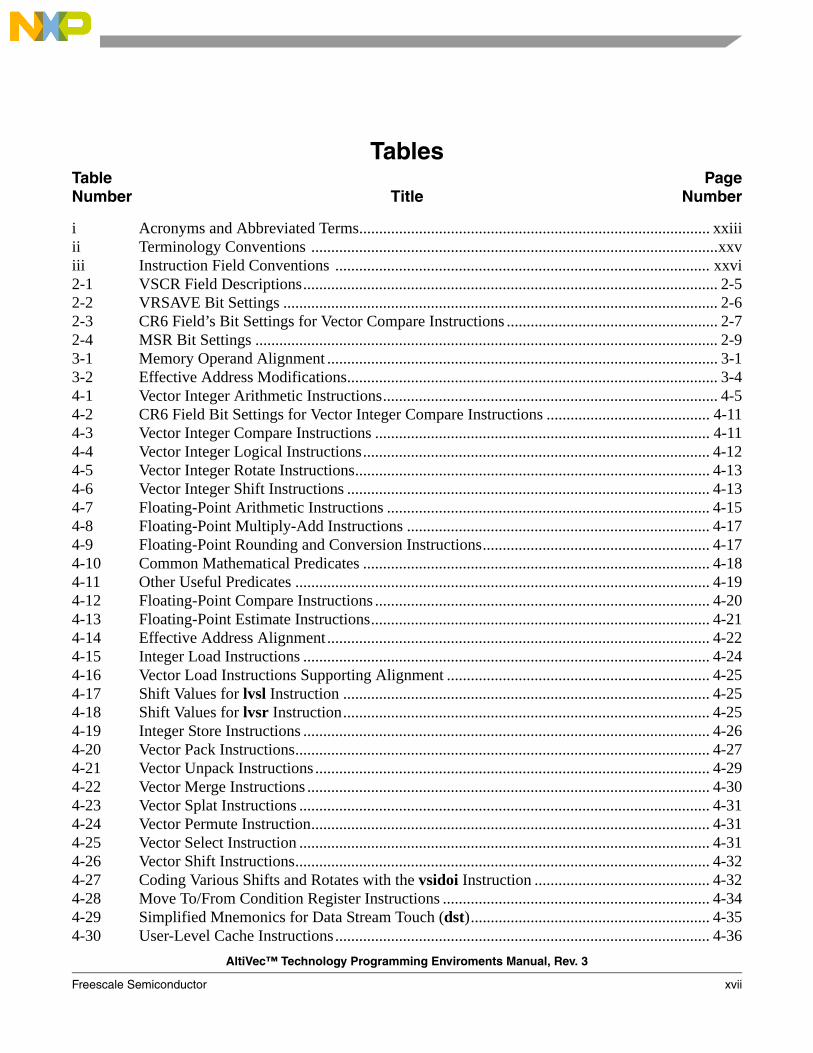
TablesTableNumber Title
PageNumber
Tables
i Acronyms and Abbreviated Terms........................................................................................ xxiiiii Terminology Conventions ......................................................................................................xxviii Instruction Field Conventions .............................................................................................. xxvi2-1 VSCR Field Descriptions........................................................................................................ 2-52-2 VRSAVE Bit Settings ............................................................................................................. 2-62-3 CR6 Field’s Bit Settings for Vector Compare Instructions ..................................................... 2-72-4 MSR Bit Settings .................................................................................................................... 2-93-1 Memory Operand Alignment .................................................................................................. 3-13-2 Effective Address Modifications............................................................................................. 3-44-1 Vector Integer Arithmetic Instructions.................................................................................... 4-54-2 CR6 Field Bit Settings for Vector Integer Compare Instructions ......................................... 4-114-3 Vector Integer Compare Instructions .................................................................................... 4-114-4 Vector Integer Logical Instructions....................................................................................... 4-124-5 Vector Integer Rotate Instructions......................................................................................... 4-134-6 Vector Integer Shift Instructions ........................................................................................... 4-134-7 Floating-Point Arithmetic Instructions ................................................................................. 4-154-8 Floating-Point Multiply-Add Instructions ............................................................................ 4-174-9 Floating-Point Rounding and Conversion Instructions......................................................... 4-174-10 Common Mathematical Predicates ....................................................................................... 4-184-11 Other Useful Predicates ........................................................................................................ 4-194-12 Floating-Point Compare Instructions .................................................................................... 4-204-13 Floating-Point Estimate Instructions..................................................................................... 4-214-14 Effective Address Alignment ................................................................................................ 4-224-15 Integer Load Instructions ...................................................................................................... 4-244-16 Vector Load Instructions Supporting Alignment .................................................................. 4-254-17 Shift Values for lvsl Instruction ............................................................................................ 4-254-18 Shift Values for lvsr Instruction............................................................................................ 4-254-19 Integer Store Instructions ...................................................................................................... 4-264-20 Vector Pack Instructions........................................................................................................ 4-274-21 Vector Unpack Instructions ................................................................................................... 4-294-22 Vector Merge Instructions ..................................................................................................... 4-304-23 Vector Splat Instructions ....................................................................................................... 4-314-24 Vector Permute Instruction.................................................................................................... 4-314-25 Vector Select Instruction ....................................................................................................... 4-314-26 Vector Shift Instructions........................................................................................................ 4-324-27 Coding Various Shifts and Rotates with the vsidoi Instruction ............................................ 4-324-28 Move To/From Condition Register Instructions ................................................................... 4-344-29 Simplified Mnemonics for Data Stream Touch (dst)............................................................ 4-354-30 User-Level Cache Instructions.............................................................................................. 4-36

AltiVec™ Technology Programming Enviroments Manual, Rev. 3
xviii Freescale Semiconductor
TablesTableNumber Title
PageNumber
5-1 AltiVec Unavailable Interrupt—Register Settings .................................................................. 5-95-2 Interrupt Priorities (Synchronous/Precise Interrupts) ........................................................... 5-116-1 Instruction Syntax Conventions .............................................................................................. 6-16-2 Notation and Conventions....................................................................................................... 6-26-3 Instruction Field Conventions................................................................................................. 6-76-4 Precedence Rules .................................................................................................................... 6-76-5 Special Values of the Element in vB..................................................................................... 6-676-6 Special Values of the Element in vB..................................................................................... 6-696-7 Special Values of the Element in vB................................................................................... 6-1236-8 Special Values of the Element in vB................................................................................... 6-132A-1 Instructions Sorted by Mnemonic in Decimal Format........................................................... A-1A-2 Instructions Sorted by Mnemonic in Binary Format ............................................................. A-6A-3 Instructions Sorted by Opcode in Decimal Format...............................................................A-11A-4 Instructions Sorted by Opcode in Binary Format ................................................................ A-16A-5 VA-Form .............................................................................................................................. A-21A-6 VX-Form.............................................................................................................................. A-21A-7 X-Form................................................................................................................................. A-24A-8 VXR-Form ........................................................................................................................... A-25A-9 AltiVec Instruction Set Legend ............................................................................................ A-26

AltiVec™ Technology Programming Enviroments Manual, Rev. 3
Freescale Semiconductor xix
About This BookThe primary objective of this manual is to help programmers provide software that is compatible with processors that implement the PowerPC™ architecture and the AltiVec™ technology. This book describes how the AltiVec technology relates to the 32-bit portions of the PowerPC architecture.
To locate any published errata or updates for this document, refer to the web at http://www.freescale.com.
This book is one of two that discuss the AltiVec technology. The two books are as follows.• AltiVec Technology Programming Interface Manual (ALTIVECPIM) is a reference guide for
high-level programmers. The AltiVec PIM describes how programmers can access AltiVec functionality from programming languages such as C and C++. The AltiVec PIM defines a programming model for use with the AltiVec instruction set. Processors that implement the PowerPC architecture use the AltiVec instruction set as an extension of the PowerPC instruction set.
• AltiVec Technology Programming Environments Manual (ALTIVECPEM) is used as a reference guide for assembler programmers. The AltiVec PEM uses a standardized format instruction to describe each instruction, showing syntax, instruction format, register translation language (RTL) code that describes how the instruction works, and a listing of which, if any, registers are affected. At the bottom of each instruction entry is a figure that shows the operations on elements within source operands and where the results of those operations are placed in the destination operand.
Because it is important to distinguish between the levels of the PowerPC architecture to ensure compatibility across multiple platforms, those distinctions are shown clearly throughout this book. This document stays consistent with the PowerPC architecture in referring to three levels, or programming environments, which are as follows:
• PowerPC user instruction set architecture (UISA)—The UISA defines the level of the architecture to which user-level software should conform. The UISA defines the base user-level instruction set, user-level registers, data types, memory conventions, and the memory and programming models seen by application programmers.
• PowerPC virtual environment architecture (VEA)—The VEA, which is the smallest component of the PowerPC architecture, defines additional user-level functionality that falls outside typical user-level software requirements. The VEA describes the memory model for an environment in which multiple processors or other devices can access external memory and defines aspects of the cache model and cache control instructions from a user-level perspective. VEA resources are particularly useful for optimizing memory accesses and for managing resources in an environment in which other processors and other devices can access external memory.Implementations that conform to the VEA also conform to the UISA but may not necessarily adhere to the OEA.

AltiVec™ Technology Programming Enviroments Manual, Rev. 3
xx Freescale Semiconductor
• PowerPC operating environment architecture (OEA)—The OEA defines supervisor-level resources typically required by an operating system. It defines the memory management model, supervisor-level registers, and the exception model. Implementations that conform to the OEA also conform to the UISA and VEA.
Most of the discussions on the AltiVec technology are at the UISA level. For ease in reference, this book and the processor reference manuals have arranged the architecture information into topics that build on one another, beginning with a description and complete summary of registers and instructions (for all three environments) and progressing to more specialized topics such as the cache, exception, and memory management models. As such, chapters may include information from multiple levels of the architecture, but when discussing OEA and VEA, the level is noted in the text.
It is beyond the scope of this manual to describe individual AltiVec technology implementations on processors that implement the PowerPC architecture. It must be kept in mind that each processor that implements the PowerPC architecture and AltiVec technology is unique in its implementation.
The information in this book is subject to change without notice, as described in the disclaimers on the title page of this book. As with any technical documentation, it is the readers’ responsibility to be sure they are using the most recent version of the documentation. For more information, contact your sales representative or visit our web site at http://www.freescale.com.
AudienceThis manual is intended for system software and hardware developers and application programmers who want to develop products using the AltiVec technology extension to the PowerPC architecture. It is assumed that the reader understands operating systems, microprocessor system design, and the basic principles of RISC processing and details of the PowerPC architecture.
This book describes how the AltiVec technology interacts with the 32-bit portions of the PowerPC architecture.
OrganizationFollowing is a summary and a brief description of the major sections of this manual:
• Chapter 1, “Overview,” is useful for those who want a general understanding of the features and functions of the AltiVec technology. This chapter provides an overview of how the AltiVec technology defines the register set, operand conventions, addressing modes, instruction set, cache model, and interrupt model.
• Chapter 2, “AltiVec Register Set,” is useful for software engineers who need to understand the PowerPC programming model for the three programming environments. The chapter also discusses the functionality of the AltiVec technology registers and how they interact with the other PowerPC registers.
• Chapter 3, “Operand Conventions,” describes how the AltiVec technology interacts with the PowerPC conventions for storing data in memory, including information regarding alignment, single-precision floating-point conventions, and big- and little-endian byte ordering.
AltiVec™ Technology Programming Enviroments Manual, Rev. 3
Freescale Semiconductor xxi
• Chapter 4, “Addressing Modes and Instruction Set Summary,” provides an overview of the AltiVec technology addressing modes and a brief description of the AltiVec technology instructions organized by function.
• Chapter 5, “Cache, Interrupts, and Memory Management,” provides a discussion of the cache and memory model defined by the VEA and aspects of the cache model that are defined by the OEA. It also describes the interrupt model defined in the UISA.
• Chapter 6, “AltiVec Instructions,” functions as a handbook for the AltiVec instruction set. Instructions are sorted by mnemonic. Each instruction description includes the instruction formats and figures where it helps in understanding what the instruction does.
• Appendix A, “AltiVec Instruction Set Listings,” list all of the AltiVec instructions, grouped according to mnemonic, opcode, and form, in both decimal and binary order.
• Appendix B, “Revision History,” lists the major differences between revisions of the AltiVec Technology Programming Environments Manual.
• This manual also includes a glossary and an index.
Suggested ReadingThis section lists additional reading that provides background for the information in this manual as well as general information about the AltiVec technology and PowerPC architecture.
General Information
The following documentation, available through Morgan-Kaufmann Publishers, 340 Pine Street, Sixth Floor, San Francisco, CA, provides useful information about the PowerPC architecture and computer architecture in general:
• The PowerPC Architecture: A Specification for a New Family of RISC Processors, Second Edition, by International Business Machines, Inc. For updates to the specification, see http://www.austin.ibm.com/tech/ppc-chg.html
• PowerPC Microprocessor Common Hardware Reference Platform: A System Architecture, by Apple Computer, Inc., International Business Machines, Inc., and Freescale Semiconductor, Inc.
• Computer Architecture: A Quantitative Approach, Third Edition, by John L. Hennessy and David A. Patterson.
• Computer Organization and Design: The Hardware/Software Interface, Third Edition, David A. Patterson and John L. Hennessy.
Related Documentation
Freescale documentation is available from the sources listed on the back cover of this manual; the document order numbers are included in parentheses for ease in ordering:
• Programming Environments Manual for 32-Bit Implementations of the PowerPC Architecture (Programming Environments Manual)—Describes resources defined by the PowerPC architecture (MPCFP32B).

AltiVec™ Technology Programming Enviroments Manual, Rev. 3
xxii Freescale Semiconductor
• Reference manuals—These manuals provide details about individual implementations and are intended for use with the Programming Environments Manual.
• Addenda/errata to reference manuals—Because some processors have follow-on parts, an addendum is provided that describes the additional features and functionality changes. These addenda are intended for use with the corresponding reference manuals.
• Hardware specifications—Hardware specifications provide specific data regarding bus timing, signal behavior, and AC, DC, and thermal characteristics, as well as other design considerations.
• Product brief—Each device has a product brief that provides an overview of its features. This document is roughly the equivalent to the overview (Chapter 1) of an implementation’s reference manual.
• Application notes—These short documents address specific design issues useful to programmers and engineers working with Freescale processors.
Additional literature is published as new processors become available. For a current list of documentation, refer to http://www.freescale.com.
ConventionsThis document uses the following notational conventions:cleared/set When a bit takes the value zero, it is said to be cleared; when it takes a value of
one, it is said to be set.mnemonics Instruction mnemonics are shown in lowercase bold italics Italics indicate variable command parameters, for example, bcctrx
Book titles in text are set in italics0x0 Prefix to denote hexadecimal number0b0 Prefix to denote binary numberrA, rB Instruction syntax used to identify a source general-purpose register (GPR)rD Instruction syntax used to identify a destination GPRfrA, frB, frC Instruction syntax used to identify a source floating-point register (FPR)frD Instruction syntax used to identify a destination FPRREG[FIELD] Abbreviations for registers are shown in uppercase text. Specific bits, fields, or
ranges appear in brackets. For example, MSR[LE] refers to the little-endian mode enable bit in the machine state register.
vA, vB, vC Instruction syntax used to identify a source vector register (VR)vD Instruction syntax used to identify a destination VRx In some contexts, such as signal encodings, an unitalicized x indicates a don’t
care. x An italicized x indicates an alphanumeric variablen An italicized n indicates an numeric variable¬ NOT logical operator
AltiVec™ Technology Programming Enviroments Manual, Rev. 3
Freescale Semiconductor xxiii
& AND logical operator| OR logical operator
Indicates reserved bits or bit fields in a register. Although these bits may be written to as ones or zeros, they are always read as zeros.
Additional conventions used with instruction encodings are described in Section 6.1, “Instruction Formats.”
Acronyms and AbbreviationsTable i contains acronyms and abbreviations that are used in this document. Note that the meanings for some acronyms (such as SDR1 and XER) are historical, and the words for which an acronym stands may not be intuitively obvious.
Table i. Acronyms and Abbreviated Terms
Term Meaning
AltiVec PEM AltiVec Technology Programming Environments Manual
AltiVec PIM AltiVec Technology Programming Interface Manual
ALU Arithmetic logic unit
BAT Block address translation
CR Condition register
CTR Count register
DABR Data address breakpoint register
DAR Data address register
DBAT Data BAT
DEC Decrementer register
DSISR Register used for determining the source of a data storage interrupt
EA Effective address
ECC Error checking and correction
FPR Floating-point register
FPSCR Floating-point status and control register
FPU Floating-point unit
GPR General-purpose register
IABR Instruction address breakpoint register
IBAT Instruction BAT
IEEE Institute of Electrical and Electronics Engineers
ITLB Instruction translation lookaside buffer
IU Integer unit
0 0 0 0
AltiVec™ Technology Programming Enviroments Manual, Rev. 3
xxiv Freescale Semiconductor
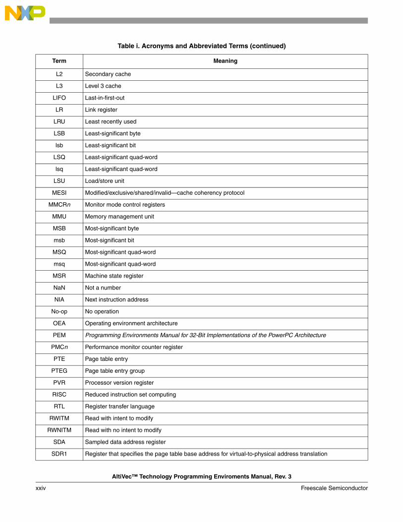
L2 Secondary cache
L3 Level 3 cache
LIFO Last-in-first-out
LR Link register
LRU Least recently used
LSB Least-significant byte
lsb Least-significant bit
LSQ Least-significant quad-word
lsq Least-significant quad-word
LSU Load/store unit
MESI Modified/exclusive/shared/invalid—cache coherency protocol
MMCRn Monitor mode control registers
MMU Memory management unit
MSB Most-significant byte
msb Most-significant bit
MSQ Most-significant quad-word
msq Most-significant quad-word
MSR Machine state register
NaN Not a number
NIA Next instruction address
No-op No operation
OEA Operating environment architecture
PEM Programming Environments Manual for 32-Bit Implementations of the PowerPC Architecture
PMCn Performance monitor counter register
PTE Page table entry
PTEG Page table entry group
PVR Processor version register
RISC Reduced instruction set computing
RTL Register transfer language
RWITM Read with intent to modify
RWNITM Read with no intent to modify
SDA Sampled data address register
SDR1 Register that specifies the page table base address for virtual-to-physical address translation
Table i. Acronyms and Abbreviated Terms (continued)
Term Meaning

AltiVec™ Technology Programming Enviroments Manual, Rev. 3
Freescale Semiconductor xxv
Terminology ConventionsTable ii lists certain terms used in this manual that differ from the architecture terminology conventions.
SIA Sampled instruction address register
SIMM Signed immediate value
SPR Special-purpose register
SRn Segment register
SRR0 Machine status save/restore register 0
SRR1 Machine status save/restore register 1
STE Segment table entry
TB Time base facility
TBL Time base lower register
TBU Time base upper register
TLB Translation lookaside buffer
UIMM Unsigned immediate value
UISA User instruction set architecture
UMMCRn User monitor mode control registers
UPMCn User performance monitor counter registers
VA Virtual address
VEA Virtual environment architecture
VPU Vector permute unit
VR Vector register
VSCR Vector status and control register
VTQ Vector touch queue
XER Register used for indicating conditions such as carries and overflows for integer operations
Table ii. Terminology Conventions
The Architecture Specification This Manual
Extended mnemonics Simplified mnemonics
Fixed-point unit (FXU) Integer unit (IU)
Privileged mode (or privileged state) Supervisor-level privilege
Problem mode (or problem state) User-level privilege
Real address Physical address
Table i. Acronyms and Abbreviated Terms (continued)
Term Meaning

AltiVec™ Technology Programming Enviroments Manual, Rev. 3
xxvi Freescale Semiconductor
Table iii describes instruction field notation conventions used in this manual.
Relocation Translation
Storage (locations) Memory
Storage (the act of) Access
Store in Write back
Store through Write through
Table iii. Instruction Field Conventions
The Architecture Specification Equivalent to:
BA, BB, BT crbA, crbB, crbD (respectively)
BF, BFA crfD, crfS (respectively)
D d
DS ds
FLM FM
FRA, FRB, FRC, FRT, FRS frA, frB, frC, frD, frS (respectively)
FXM CRM
/, //, /// 0...0 (shaded)
RA, RB, RT, RS rA, rB, rD, rS (respectively)
SI SIMM
U IMM
UI UIMM
VA, VB, VT, VS vA, vB, vD, vS (respectively)
VEC AltiVec technology
Table ii. Terminology Conventions (continued)
The Architecture Specification This Manual
AltiVec™ Technology Programming Enviroments Manual, Rev. 3
Freescale Semiconductor 1-1
Chapter 1 OverviewThis chapter provides an overview of the AltiVec™ technology, including general concepts which help in understanding the features that AltiVec technology provides. There is also information on how AltiVec technology works with PowerPC™ architecture.
1.1 OverviewAltiVec technology provides a software model that accelerates the performance of various software applications as it runs on reduced instruction set computing (RISC) microprocessors. AltiVec technology extends the instruction set architecture (ISA) of PowerPC architecture. AltiVec ISA is based on separate vector/SIMD-style (single instruction stream, multiple data streams) execution units that have high data parallelism. That is, AltiVec technology operates on multiple data items in a single instruction which allows for a highly efficient way to process large quantities of information. High degrees of parallelism are achievable with simple in-order instruction dispatch and low-instruction time processing. However, the ISA is designed so as not to impede additional parallelism through dispatch to multiple execution units or multithreaded execution unit pipelines.
AltiVec technology is an architecture that defines a set of registers and execution units which can be used in conjunction with the PowerPC architecture. All instructions are designed to be easily pipelined with pipeline latencies no greater than the scalar, double-precision, floating-point multiply-add. There are no operating mode switches which make interleaving of instructions with the existing floating-point and integer instructions possible. The vector unit minimizes exceptions and has few shared resources. This requires it to be tightly synchronized with other execution units that prevent delays in executing instructions.
AltiVec technology’s SIMD-style extension provides an approach to accelerating the processing of data streams. That is, in SIMD parallel processing, the vector unit will fetch and interpret instructions and process multiple pieces of data simultaneously. By processing whole streams of data at once, it provides a fast and efficient was to manipulate large quantities of information. AltiVec instructions provide a significant speedup for communications, multimedia, and other performance-driven applications by using the data-level parallelism and keeping processing of data to the vector register file. By having separate register files, the execution units data accesses by different register files can be done concurrently. The data stream engine in AltiVec supports data-intensive prefetching, minimizing latency in memory access bottlenecks. By using the SIMD parallelism in AltiVec technology, performance can be accelerated on processors that implement the PowerPC architecture to a level that allows real-time processing of one or more data streams at the same time.

Overview
AltiVec™ Technology Programming Enviroments Manual, Rev. 3
1-2 Freescale Semiconductor
A majority of audio and visual applications require no more than 8- or 16-bit data types to represent satisfactory color and sound. AltiVec ISA can help accelerate the processing of the following types of applications:
• Voice over IP (VoIP). VoIP transmits voice as compressed digital data packets over the Internet.• Access Concentrators/DSLAMS. An access concentrator strips data traffic off POTS lines and
inserts it onto the Internet. Digital subscriber loop access multiplexer (DSLAM) pulls data off at a switch and immediately routes it to the Internet. This allows it to concentrate ADSL digital traffic at the switch and off-load the network.
• Speech recognition. Speech processing allows voice recognition for use in applications such as directory assistance and automatic dialing.
• Voice/sound processing (audio encode and decode): Voice processing uses signal processing to improve sound quality on lines.
• Communications:— Multi-channel modems— Modem banks can use AltiVec technology to replace signal processors in DSP farms
• 2D and 3D graphics: Arcade-type games• Image and video processing: JPEG, filters• Echo cancellation. Echo cancellation is used to eliminate echo on long delay calls
(250–500 milliseconds, as in satellite communications).• Array number processing• Basestation processing: Cellular basestation compresses digital voice data for transmission within
the Internet.• Video conferencing: H.261, H.263
In this document, the term ‘implementation’ refers to a hardware device (typically a microprocessor) that complies with PowerPC architecture.
AltiVec technology can be used as an extension to various RISC microprocessors; however, in this book it is discussed within the context of PowerPC architecture, described as follows:
• Programming model— Instruction set. The AltiVec instruction set specifies instructions that extend the PowerPC
instruction set. These instructions are organized similar to PowerPC instructions (vector integer, vector floating-point, vector load/store, and vector permutation and formatting instructions). The specific instructions, and the forms used for encoding them, are provided in Appendix A, “AltiVec Instruction Set Listings.”
— Register set. The AltiVec programming model defines new AltiVec registers, additions to the PowerPC register set, and how existing PowerPC registers are affected by the AltiVec technology. The model also addresses memory conventions including details regarding the byte ordering for quad words.
• Memory model. AltiVec technology specifies additional cache management instructions. That is, AltiVec instructions can control software-directed data prefetching.

Overview
AltiVec™ Technology Programming Enviroments Manual, Rev. 3
Freescale Semiconductor 1-3
• Interrupt model. AltiVec technology provides very few interrupts, so processing is efficient. Among the few interrupts are an AltiVec unavailable (VUI) interrupt and a data storage interrupt.
• Memory management model. The memory model for AltiVec technology is the same as for PowerPC architecture. AltiVec memory accesses are always assumed to be aligned. If an operand is misaligned, additional AltiVec instructions can be used to ensure that the operand is placed correctly in the vector register.
• Time-keeping model. The PowerPC time-keeping model is not affected by AltiVec technology.
To locate published errata or updates for this document, refer to the website at http://www.freescale.com.
1.2 AltiVec Technology OverviewAltiVec technology expands PowerPC architecture through the addition of a 128-bit vector execution unit, which operates concurrently with the existing integer- and floating-point units. The dispatch unit can issue more than one instruction at a time so there is no penalty for mingling different types of instructions. A new vector execution unit can provide both a vector permute unit (VPERM) and vector arithmetic logical unit (VALU). By having a separate permute unit, data reorganization instructions can proceed concurrently with arithmetic instructions.
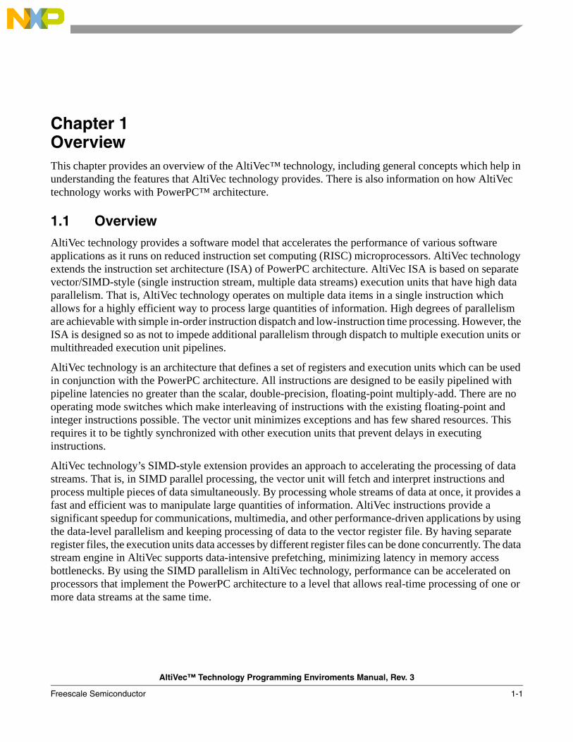
AltiVec technology can be thought of as a set of registers and execution units that can be added to PowerPC architecture in a manner analogous to the addition of floating-point units. Floating-point units were added to provide support for high-precision scientific calculations, and AltiVec technology is added to PowerPC architecture to accelerate the next level of performance-driven, high-bandwidth communications and computing applications. Figure 1-1 provides a high-level overview of the PowerPC architecture with the AltiVec technology.
AltiVec technology is purposefully simple so that there are minimal exceptions, no hardware misaligned access support, and no complex functions. AltiVec technology is scaled down to the necessary pieces only, in order to facilitate efficient cycle time, latency, and throughput on hardware implementations.
AltiVec technology defines the following:• Fixed 128-bit-wide vector length that can be subdivided into sixteen 8-bit bytes, eight 16-bit
half-words, or four 32-bit words• Vector register file (VRF) architecturally separate from floating-point registers (FPRs) and
general-purpose registers (GPRs)• Vector integer and floating-point arithmetic• Four operands for most instructions (three source operands and one result)• Saturation clamping, that is, unsigned results are clamped to zero on underflow and to the
maximum positive integer value (2n–1), for example, 255 for byte fields on overflow. For signed results, saturation clamps results to the smallest representable negative number (–2n–1, for example, –128 for byte fields) on underflow, and to the largest representable positive number (2n–01–1), for example, +127 for byte fields on overflow.
• Operations selected based on utility to digital signal processing algorithms (including 3D)
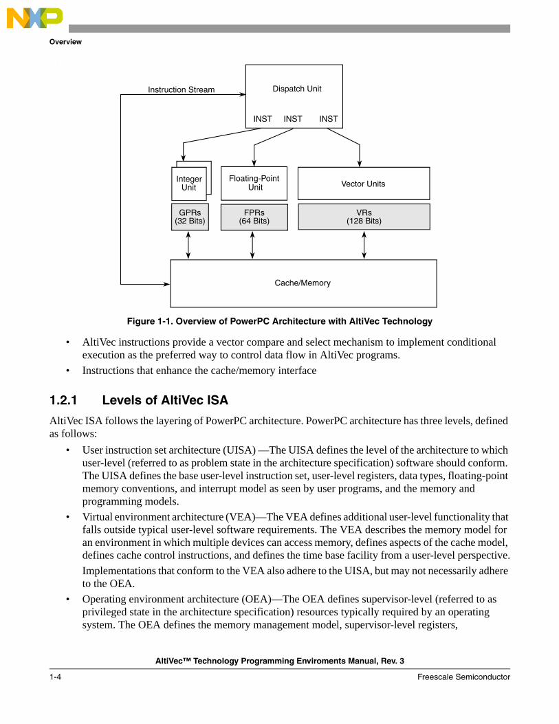
Overview
AltiVec™ Technology Programming Enviroments Manual, Rev. 3
1-4 Freescale Semiconductor
.
Figure 1-1. Overview of PowerPC Architecture with AltiVec Technology
• AltiVec instructions provide a vector compare and select mechanism to implement conditional execution as the preferred way to control data flow in AltiVec programs.
• Instructions that enhance the cache/memory interface
1.2.1 Levels of AltiVec ISA
AltiVec ISA follows the layering of PowerPC architecture. PowerPC architecture has three levels, defined as follows:
• User instruction set architecture (UISA) —The UISA defines the level of the architecture to which user-level (referred to as problem state in the architecture specification) software should conform. The UISA defines the base user-level instruction set, user-level registers, data types, floating-point memory conventions, and interrupt model as seen by user programs, and the memory and programming models.
• Virtual environment architecture (VEA)—The VEA defines additional user-level functionality that falls outside typical user-level software requirements. The VEA describes the memory model for an environment in which multiple devices can access memory, defines aspects of the cache model, defines cache control instructions, and defines the time base facility from a user-level perspective.Implementations that conform to the VEA also adhere to the UISA, but may not necessarily adhere to the OEA.
• Operating environment architecture (OEA)—The OEA defines supervisor-level (referred to as privileged state in the architecture specification) resources typically required by an operating system. The OEA defines the memory management model, supervisor-level registers,
Dispatch Unit
Integer Floating-PointVector UnitsUnit
VRs
INST INST INST
Cache/Memory
Unit
FPRs(32 Bits) (64 Bits) (128 Bits)
Instruction Stream
GPRs

Overview
AltiVec™ Technology Programming Enviroments Manual, Rev. 3
Freescale Semiconductor 1-5
synchronization requirements, and the exception model. The OEA also defines the time base feature from a supervisor-level perspective.Implementations that conform to the OEA also conform to the UISA and VEA.
AltiVec technology defines instructions at the UISA and VEA levels. There are no AltiVec instructions defined at the OEA level. The distinctions between the levels are noted in the text throughout this book. The PowerPC architecture mode and instructions are described from a 32-bit perspective.
1.2.2 Features Not Defined by AltiVec ISA
Because flexibility is an important design goal of AltiVec technology, there are many aspects of the microprocessor design, typically relating to the hardware implementation, that AltiVec ISA does not define. For example, the number and the nature of execution units are not defined. AltiVec ISA is a vector/SIMD architecture, and as such makes it easier to implement pipelining instructions and parallel execution units to maximize instruction throughput. However, AltiVec ISA does not define the internal hardware details of implementations. For example, one processor may use a simple implementation having two vector execution units, whereas another may provide a bigger, faster microprocessor design with several concurrently pipelined vector arithmetic logical units (ALUs) with separate load/store units (LSUs) and prefetch units.
1.3 AltiVec Architectural ModelThis section provides overviews of aspects defined by AltiVec ISA, following the same order as the rest of this book. The topics are as follows:
• Registers and programming model• Operand conventions• Addressing modes and instruction set• Cache, interrupts, and memory management models
1.3.1 AltiVec Registers and Programming Model
In AltiVec technology, the ALU operates on from one to three source vectors and produces a single destination vector on each instruction. The ALU is a SIMD-style arithmetic unit that performs the same operation on all the data elements comprising each vector. This scheme allows efficient code scheduling in a highly parallel processor. Load and store instructions are the only instructions that transfer data between registers and memory. The vector unit and vector register file are shown in Figure 1-2.
The ALU is a SIMD-style unit in which an instruction performs operations in parallel with the data elements that comprise each vector. Architecturally, the vector register file (VRF) is separate from the GPRs and FPRs. The AltiVec programming model incorporates the 32 registers of the VRFs; each register is 128 bits wide.

Overview
AltiVec™ Technology Programming Enviroments Manual, Rev. 3
1-6 Freescale Semiconductor
Figure 1-2. AltiVec Top-Level Diagram
1.3.2 Operand Conventions
Operand conventions define how data is stored in vector registers and memory.
1.3.2.1 Byte Ordering
The default mapping for AltiVec ISA is PowerPC big-endian, but AltiVec ISA provides the option of operating in either big- or little-endian mode. The endian support of PowerPC architecture does not address any data element larger than a double word; the basic memory unit for vectors is a quad word.
Big-endian byte ordering is shown in Figure 1-3..
Quad Word
Word 0 Word 1 Word 2 Word 3
Half-Word 0 Half-Word 1 Half-Word 2 Half-Word 3 Half-Word 4 Half-Word 5 Half-Word 6 Half-Word 7
Byte 0
Byte 1
Byte 2
Byte 3
Byte 4
Byte 5
Byte 6
Byte 7
Byte 8
Byte 9
Byte 10
Byte 11
Byte 12
Byte 13
Byte 14
Byte 15
0 8 16 24 32 40 48 56 64 72 80 88 96 104 112 120 127
↑MSB(High Order)
↑LSB(Low
Order)Figure 1-3. Big-Endian Byte Ordering for a Vector Register
Vector Register File (VRF)
128
VR0
VR1
VR2
VR30
VR31
128 128 128
Result/Destination
Vector Unit
Vector Register

Overview
AltiVec™ Technology Programming Enviroments Manual, Rev. 3
Freescale Semiconductor 1-7
As shown in Figure 1-3, the elements in vector registers are numbered using big-endian byte ordering. For example, the high-order (or most significant) byte element is numbered 0 and the low-order (or least significant) byte element is numbered 15.
When defining high order and low order for elements in a vector register, be careful not to confuse its meaning based on the bit numbering. That is, in Figure 1-4, the high-order half-word for word 0 (bits 0–31) would be half-word 0 (bits 0–15), and the low-order half-word for word 0 would be half-word 1 (bits 16–31).
In big-endian mode, an AltiVec quad word load instruction for which the effective address (EA) is quad-word aligned places the byte addressed by EA into byte element 0 of the target vector register. The byte addressed by EA + 1 is placed in byte element 1, and so forth. Similarly, an AltiVec quad word store instruction for which the EA is quad word-aligned places byte element 0 of the source vector register into the byte addressed by EA. Byte element 1 is placed into the byte addressed by EA + 1, and so forth.
1.3.2.2 Floating-Point Conventions
AltiVec ISA basically has two modes for floating-point, that is a Java-/IEEE-/C9X-compliant mode or a possibly faster non-Java/non-IEEE mode. AltiVec ISA conforms to the Java Language Specification 1 (hereafter referred to as Java), that is a subset of the default environment specified by the IEEE standard (ANSI/IEEE Standard 754-1985, IEEE Standard for Binary Floating-Point Arithmetic). For aspects of floating-point behavior that are not defined by Java but are defined by the IEEE standard, AltiVec ISA conforms to the IEEE standard. For aspects of floating-point behavior that are defined neither by Java nor by the IEEE standard but are defined by the C9X Floating-Point Proposal WG14/N546 X3J11/96-010 (Draft 2/26/96) (hereafter, referred to as C9X), AltiVec ISA conforms to C9X when in Java-compliant mode.
1.3.3 AltiVec Addressing Modes
As with PowerPC instructions, AltiVec instructions are encoded as single-word (32-bit) instructions. Instruction formats are consistent among all instruction types, permitting decoding to be parallel with operand accesses. This fixed instruction length and consistent format simplifies instruction pipelining. AltiVec load, store, and stream prefetch instructions use secondary opcodes in primary opcode 31 (0b011111). AltiVec ALU-type instructions use primary opcode 4 (0b000100).
AltiVec ISA supports both intra-element and interelement operations. In an intra-element operation, elements work in parallel with the corresponding elements from multiple source operand registers and place the results in the corresponding fields in the destination operand register. An example of an intra-element operation is the Vector Add Signed Word Saturate (vaddsws) instruction shown in Figure 1-5.
Word 0
High-Order Half-Word Low-Order Half-Word0 15 16 31
Figure 1-4. Bit Ordering

Overview
AltiVec™ Technology Programming Enviroments Manual, Rev. 3
1-8 Freescale Semiconductor
Figure 1-5. Intra-Element Example, vaddsbs
In this example, the 16 elements (8 bits per element) in register vA are added to the corresponding 16 elements (8 bits per element) in register vB and the 16 results are placed in the corresponding elements in register vD.
In interelement operations data paths cross over. That is, different elements from each source operand are used in the resulting destination operand. An example of an interelement operation is the Vector Permute (vperm) instruction shown in Figure 1-6.
Figure 1-6. Interelement Example, vperm
In this example, vperm allows any byte in the two source vector registers (vA and vB) to be copied to any byte in the destination vector register, vD. The bytes in a third source vector register (vC) specify from which byte in the first two source vector registers the corresponding target byte is to be copied. So in the interelement example, the elements from the source vector registers do not have corresponding elements that operate on the destination register.
Most arithmetic and logical instructions are intra-element operations. The crossover data paths have been restricted as much as possible to the interelement manipulation instructions (unpack, pack, permute, etc.) with the idea to implement the ALU and shift/permute as separate execution units. The following list of instructions distinguishes between intra-element and interelement instructions:
• Vector intra-element instructions— Vector integer instructions
– Vector integer arithmetic instructions– Vector integer compare instructions– Vector integer rotate and shift instructions
— Vector floating-point instructions– Vector floating-point arithmetic instructions
0Element→ 1 2 3 4 5 6 7 8 9 10 11 12 13 14 15
+ +++++++++++++++
vA
vB
vD
0Element→ 1 2 3 4 5 6 7 8 9 10 11 12 13 14 15
vC1 14 18 10 16 15 19 1A 1C 1C 1C 13 8 1D 1B E
vA
vB
vD
0 1 2 3 4 5 6 7 8 9 A B C D E F
10 12 13 14 15 16 17 18 19 1A 1B 1C 1D 1F11 1E

Overview
AltiVec™ Technology Programming Enviroments Manual, Rev. 3
Freescale Semiconductor 1-9
– Vector floating-point rounding and conversion instructions– Vector floating-point compare instruction– Vector floating-point estimate instructions
— Vector memory access instructions • Vector interelement instructions
— Vector alignment support instructions— Vector permutation and formatting instructions
– Vector pack instructions– Vector unpack instructions– Vector merge instructions– Vector splat instructions– Vector permute instructions– Vector shift left/right instructions
1.3.4 AltiVec Instruction Set
Although these categories are not defined by AltiVec ISA, AltiVec instructions can be grouped as follows:• Vector integer arithmetic instructions—These instructions are defined by the UISA. They include
computational, logical, rotate, and shift instructions.— Vector integer arithmetic instructions— Vector integer compare instructions— Vector integer logical instructions— Vector integer rotate and shift instructions
• Vector floating-point arithmetic instructions—These include floating-point arithmetic instructions defined by the UISA.— Vector floating-point arithmetic instructions— Vector floating-point multiply/add instructions— Vector floating-point rounding and conversion instructions— Vector floating-point compare instruction— Vector floating-point estimate instructions
• Vector load and store instructions—These include load and store instructions for vector registers defined by the UISA.
• Vector permutation and formatting instructions—These instructions are defined by the UISA.– Vector pack instructions– Vector unpack instructions– Vector merge instructions– Vector splat instructions– Vector permute instructions
Overview
AltiVec™ Technology Programming Enviroments Manual, Rev. 3
1-10 Freescale Semiconductor
– Vector select instructions– Vector shift instructions
• Processor control instructions—These instructions are used to read and write from the AltiVec status and control register (VSCR). These instructions are defined by the UISA.
• Memory control instructions—These instructions are used for managing of caches (user level and supervisor level). The instructions are defined by VEA and include data stream instructions.
1.3.5 AltiVec Cache Model
AltiVec ISA defines several instructions for enhancements to cache management. These instructions allow software to indicate to the cache hardware how it should prefetch and prioritize writeback of data. The AltiVec ISA does not define hardware aspects of cache implementations.
1.3.6 AltiVec Interrupt Model
AltiVec vector instructions generate very few interrupts. Data stream instructions will never cause an interrupt themselves. Vector load and store instructions that attempt to access a direct-store segment will cause a data storage interrupt.
The AltiVec unit does not report IEEE interrupts; there are no status flags and the unit has no architecturally visible traps. Default results are produced for all exception conditions as specified first by the Java specification. If no default exists, the IEEE standard’s default is used. Then, if no default exists, the C9X default is used.
Interrupts have been minimized so that the vector unit does not have to be tightly synchronized with the existing floating-point and integer units. By simplifying the communications path with other units there can be fine grain interleaving of instructions that increases the instruction throughput.
1.3.7 Memory Management Model
In a processor that implement the PowerPC architecture the MMU’s primary functions are to translate logical (effective) addresses to physical addresses for memory accesses and I/O accesses (most I/O accesses are assumed to be memory-mapped) and to provide access protection on a block or page basis. Some protection is also available even if translation is disabled. Typically, it is not programmable. The AltiVec ISA does not provide any additional instructions to the PowerPC memory management model, but AltiVec instructions have options to ensure that an operand is correctly placed in a vector register or in memory.

AltiVec™ Technology Programming Enviroments Manual, Rev. 3
Freescale Semiconductor 2-1
Chapter 2 AltiVec Register SetThis chapter describes the register organization defined by AltiVec technology. It also describes how AltiVec instructions affect some of the registers in the PowerPC architecture. AltiVec Instruction Set Architecture (ISA) defines register-to-register operations for all computational instructions. Source data for these instructions is accessed from the on-chip vector registers (VRs) or are provided as immediate values embedded in the opcode. Architecturally, the VRs are separate from the general-purpose registers (GPRs) and floating-point registers (FPRs). Data is transferred between memory and vector registers with explicit AltiVec load and store instructions only.
Note that the handling of reserved bits in any register is implementation-dependent. Software is permitted to write any value to a reserved bit in a register. However, a subsequent reading of the reserved bit returns 0 if the value last written to the bit was 0 and returns an undefined value (may be 0 or 1), otherwise. This means that even if the last value written to a reserved bit was 1, reading that bit may return 0.
NOTEIt is strongly encouraged that software does not write to reserved bit registers.
2.1 Overview of AltiVec and PowerPC RegistersThe addition of AltiVec technology adds some additional new registers as well as affecting bit settings in some of the PowerPC registers when AltiVec instructions are executed. Figure 2-1 shows a graphic representation of the entire PowerPC register set and how the AltiVec register set resides within the PowerPC architecture. The PowerPC registers affected by AltiVec instructions are shaded and the AltiVec registers are highlighted as well. Note that a processor that implements the PowerPC architecture may have additional registers specific only to that processor.
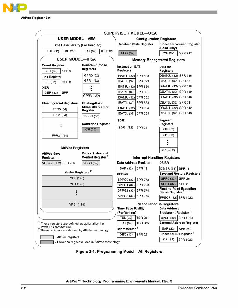
AltiVec Register Set
AltiVec™ Technology Programming Enviroments Manual, Rev. 3
2-2 Freescale Semiconductor
Figure 2-1. Programming Model—All Registers
IBAT0U (32)
IBAT0L (32)
IBAT1U (32)
IBAT1L (32)
IBAT2U (32)
IBAT2L (32)
IBAT3U (32)
IBAT3L (32)
GPR0 (32)
GPR1 (32)
GPR31 (32)
DBAT0U (32)
DBAT0L (32)
DBAT1U (32)
DBAT1L (32)
DBAT2U (32)
DBAT2L (32)
DBAT3U (32)
DBAT3L (32)
1 These registers are defined as optional by the PowerPC architecture.
2 These registers are defined by AltiVec technology.
DSISRData Address Register
SPRGs
Interrupt Handling Registers
Save and Restore Registers
Instruction BATRegisters
Data BATRegisters
Memory Management Registers
Machine State Register
MSR (32)
Processor Version Register (Read Only)
SPR 287PVR (32)
Configuration Registers
USER MODEL—UISA
Condition Register
General-PurposeRegisters
SPR 8
Link Register
LR (32)
SUPERVISOR MODEL—OEA
Decrementer 1
External Address Register1
EAR (32)
SPR 9
Count Register
Miscellaneous Registers
SegmentRegisters
CR (32)
Vector Registers 2
Time Base Facility(For Writing) 1
USER MODEL—VEA
TBL (32) TBR 268
Time Base Facility (For Reading)
CTR (32)
TBU (32) TBR 269
SPR 528
SPR 529
SPR 530
SPR 531
SPR 532
SPR 533
SPR 534
SPR 535
SPR 536
SPR 537
SPR 538
SPR 539
SPR 540
SPR 541
SPR 542
SPR 543
SDR1 (32) SPR 25
SPRG0 (32)
SPRG1 (32)
SPRG2 (32)
SPRG3 (32)
SPR 272
SPR 273
SPR 274
SPR 275
DAR (32) DSISR (32)SPR 19 SPR 18
SRR0 (32) SPR 26
SRR1 (32) SPR 27
SPR 282
TBL (32) TBR 284
TBU (32) TBR 285
DEC (32) SPR 22
Data AddressBreakpoint Register 1
DABR (32) SPR 1013
Vector Status and Control Register 2
VSCR (32)
Processor ID Register 1
PIR (32) SPR 1023
AltiVec Registers
AltiVec Save Register 2
SPR 256
Floating-Point Registers
FPR0 (64)
FPR1 (64)
FPR31 (64)
2
VR0 (128)
VR1 (128)
VR31 (128)
= AltiVec registers
= PowerPC registers used in AltiVec technology
SDR1
Floating-Point Exception Cause Register 1
FPECR (32) SPR 1022
SPR 1
XER
XER (32)
Floating-Point Status and Control Register
FPSCR (32)
Memory Management Registers
VRSAVE (32)
SR0 (32)
SR1 (32)
SR15 (32)

AltiVec Register Set
AltiVec™ Technology Programming Enviroments Manual, Rev. 3
Freescale Semiconductor 2-3
2.2 AltiVec Register Set OverviewAltiVec registers, shown in Figure 2-2, can be accessed by user- or supervisor-level instructions. The vector registers (VRs) are accessed as instruction operands. Access to the registers can be explicit (that is, through the use of specific instructions for that purpose such as Move from Vector Status and Control Register (mfvscr) and Move to Vector Status and Control Register (mtvscr) instructions) or implicit as part of the execution of an instruction. The VRs are accessed both explicitly and implicitly.
The number to the right of the register name indicates the number used in the syntax of the instruction operands to access the register (for example, the number used to access the VRSAVE is SPR 256).
Figure 2-2. AltiVec Register Set
The user-level registers can be accessed by all software with either user or supervisor privileges. The user-level register set for AltiVec technology includes the following:
• Vector registers (VRs): The vector register file consists of 32 VRs designated as VR0–VR31. The VRs serve as vector source and vector destination registers for all vector instructions. See Section 2.3.2, “Vector Status and Control Register (VSCR),” for more information.
• Vector status and control register (VSCR): The VSCR contains the non-Java and saturation bit with the remaining bits being reserved. See Section 2.3.2, “Vector Status and Control Register (VSCR),” for more details.
• Vector save/restore register (VRSAVE): The VRSAVE assists the application and operating system software in saving and restoring the architectural state across context-switched events. The bits in the VRSAVE can indicate whether the vector register is live (1) or dead (0). See Section 2.3.3, “Vector Save/Restore Register (VRSAVE),” for more information.
2.3 Registers Defined by AltiVec ISAAltiVec ISA has defined several registers. The new AltiVec registers for the most part only interact with AltiVec instructions, with the exception of the VRSAVE register that is read or written by the PowerPC instructions mfspr or mtspr, respectively.
Vector Registers
VR1
Vector Status and Control Register
VSCR
Vector Save/Restore Register
VRSAVE SPR 256
0 31
310
0 128
VR0
VR31

AltiVec Register Set
AltiVec™ Technology Programming Enviroments Manual, Rev. 3
2-4 Freescale Semiconductor
2.3.1 AltiVec Vector Register File (VRF)
The VRF, shown in Figure 2-3, has 32 registers, each 128 bits wide. Each vector register can hold sixteen 8-bit elements, eight 16-bit elements, or four 32-bit elements.
Figure 2-3. Vector Registers (VRs)
The vector registers are accessed as vector instruction operands. Access to registers are explicit as part of the execution of an AltiVec instruction.
2.3.2 Vector Status and Control Register (VSCR)
The vector status and control register (VSCR) is a 32-bit vector register (not an SPR) that is read and written in a manner similar to the FPSCR in the PowerPC scalar floating-point unit. The VSCR is shown in Figure 2-4.
0 1 2 3 4 5
Field Reserved NJ Reserved SAT
Reset Implementation Specific
R/W R/W with mfvscr or mtvscr Instruction
Figure 2-4. Vector Status and Control Register (VSCR)
VR0
VR1
VR2
VR30
VR31
VR3
32 Bits
16 Bits
8 Bits
128 Bits
32Vector
Registers
1 9 10 11 12 13 14 15 16
1
1
2
2
2
3
3
3
4
4
4
5
5
6
6
7
7
8
8
0 128
Sixteen 8-Bit Elements
Eight 16-Bit Elements
Four 32-Bit Elements
VR4
VR5

AltiVec Register Set
AltiVec™ Technology Programming Enviroments Manual, Rev. 3
Freescale Semiconductor 2-5
The VSCR has two defined bits, the AltiVec non-Java mode (NJ) bit (VSCR[15]) and the AltiVec saturation (SAT) bit (VSCR[31]); the remaining bits are reserved.
Special instructions Move from Vector Status and Control Register (mfvscr) and Move to Vector Status and Control Register (mtvscr) are provided to move the contents of VSCR from and to a vector register. When moved to or from a vector register, the 32-bit VSCR is right-justified in the 128-bit vector register. When moved to a vector register, the upper 96 bits VRn [0–95] of the vector register are cleared, so the VSCR in a vector register looks as shown in Figure 2-5.
VSCR bit settings are shown in Table 2-1.
0 95 96 110 111 112 126 127
Reserved Reserved NJ Reserved SAT
Figure 2-5. 32-Bit VSCR Moved to a 128-Bit Vector Register
Table 2-1. VSCR Field Descriptions
Bit Name Description
0–14 — ReservedThe handling of reserved bits is the same as that for other PowerPC registers. Software is permitted to write any value to such a bit. A subsequent reading of the bit returns 0, if the value last written to the bit was 0 and returns an undefined value (0 or 1), otherwise.
15 NJ Non-JavaThis bit determines whether AltiVec floating-point operations are performed in a Java-IEEE-C9X-compliant mode or a possibly faster non-Java/non-IEEE mode.0 The Java-IEEE-C9X-compliant mode is selected. Denormalized values are handled as specified by Java,
IEEE, and the C9X standard.1 The non-Java/non-IEEE-compliant mode is selected. If an element in a source vector register contains a
denormalized value, the value 0 is used instead. If an instruction causes an underflow exception, the corresponding element in the target VR is cleared to 0. In both cases, the 0 has the same sign as the denormalized or underflowing value.
This mode is described in detail in the floating–point overview, Section 3.2.1, “Floating-Point Modes.”
16–30 — ReservedThe handling of reserved bits is the same as that for other PowerPC registers. Software is permitted to write any value to such a bit. A subsequent reading of the bit returns 0, if the value last written to the bit was 0 and returns an undefined value (0 or 1), otherwise.
31 SAT Saturation A sticky status bit indicating that some field in a saturating instruction saturated since the last time SAT was cleared. In other words, when SAT = 1 it remains set to 1 until it is cleared to 0 by an mtvscr instruction. For further discussion refer to Section 4.2.1.1, “Saturation Detection.”0 Indicates no saturation occurred; mtvscr can explicitly clear this bit.1 The AltiVec saturate instruction is set when saturation occurs for the results of one of AltiVec instructions
having saturate in its name as follows:Move to VSCR (mtvscr)Vector Add Integer with Saturation (vaddubs, vadduhs, vadduws, vaddsbs, vaddshs, vaddsws)Vector Subtract Integer with Saturation (vsububs, vsubuhs, vsubuws, vsubsbs, vsubshs, vsubsws)Vector Multiply-Add Integer with Saturation (vmhaddshs, vmhraddshs)Vector Multiply-Sum with Saturation (vmsumuhs, vmsumshs, vsumsws)Vector Sum-Across with Saturation (vsumsws, vsum2sws, vsum4sbs, vsum4shs, vsum4ubs)Vector Pack with Saturation (vpkuhus, vpkuwus, vpkshus, vpkswus, vpkshss, vpkswss)Vector Convert to Fixed-Point with Saturation (vctuxs, vctsxs)

AltiVec Register Set
AltiVec™ Technology Programming Enviroments Manual, Rev. 3
2-6 Freescale Semiconductor
The mtvscr is context synchronizing. This implies that all AltiVec instructions logically preceding an mtvscr in the program flow execute in the architectural context (NJ mode) that existed before completion of mtvscr, and that all instructions logically following after mtvscr execute in the new context (NJ mode) established by the mtvscr.
After an mfvscr instruction executes, the result in the target vector register is architecturally precise. That is, it reflects all updates to the SAT bit that could have been made by vector instructions logically preceding it in the program flow, and further, it will not reflect any SAT updates that may be made to it by vector instructions logically following it in the program flow. Because it is context synchronizing, mfvscr can be much slower than typical AltiVec instructions, and, therefore, care must be taken in reading it to avoid performance problems.
2.3.3 Vector Save/Restore Register (VRSAVE)
The VRSAVE register, shown in Figure 2-6, is a user-level 32-bit SPR used to assist in application and operating system software in saving and restoring the architectural state across process context-switched events. The VRSAVE is SPR 256 and is entirely maintained and managed by software.
VRSAVE bit settings are shown in Figure 2-2.
The VRSAVE register can be accessed only by the mfspr and mtspr instructions. Each bit in this register corresponds to a vector register (VR) and indicates whether the corresponding register contains data that is currently in use by the executing process. Therefore, the operating system needs to save and restore only those VRs when an interrupt occurs. If this approach is taken, it must be applied rigorously; if a program fails to indicate that a given VR is in use, software errors may occur that are difficult to detect and correct
0 1 2 3 4 5 6 7 8 9 10 11 12 13 14 15
Field VR0 VR1 VR2 VR3 VR4 VR5 VR6 VR7 VR8 VR9 VR10 VR11 VR12 VR13 VR14 VR15
Reset 0000_0000_0000_0000
R/W R/W with mfspr or mtspr Instruction
16 17 18 19 20 21 22 23 24 25 26 27 28 29 30 31
Field VR16 VR17 VR18 VR19 VR20 VR21 VR22 VR23 VR24 VR25 VR26 VR27 VR28 VR29 VR30 VR31
Reset 0000_0000_0000_0000
R/W R/W with mfspr or mtspr Instructions
SPR SPR 256
Figure 2-6. Vector Save/Restore Register (VRSAVE)
Table 2-2. VRSAVE Bit Settings
Bits Name Description
0–31 VRn Each bit in the VRSAVE register indicates whether the corresponding VR contains data in use by the executing process.0 VRn is not being used for the current process1 VRn is using VRn for the current process

AltiVec Register Set
AltiVec™ Technology Programming Enviroments Manual, Rev. 3
Freescale Semiconductor 2-7
because they are timing-dependent. Some operating systems save and restore VRSAVE only for programs that also use other AltiVec registers.
2.4 Additions to PowerPC UISA RegistersThe PowerPC UISA registers can be accessed by either user- or supervisor-level instruction. The one register affected by AltiVec architecture is the condition register (CR). The CR is a 32-bit register, divided into eight 4-bit fields, CR0–CR7, that reflects the results of certain arithmetic operations and provides a mechanism for testing and branching. For more details refer to Chapter 2, “Register Set,” in the Programming Environments Manual for 32-Bit Implementations of the PowerPC Architecture.
2.4.1 PowerPC Condition Register
The PowerPC condition register (CR) is a 32-bit register that reflects the result of certain operations and provides a mechanism for testing and branching. For AltiVec ISA, the CR6 field can optionally be used, that is, if an AltiVec instruction field’s record bit (Rc) is set in a vector compare instruction. The CR6 field is updated. The CR is divided into eight 4-bit fields, CR0–CR7, as shown in Figure 2-7.
For more details on the CR see Chapter 2, “Register Set,” in the Programming Environments Manual for 32-Bit Implementations of the PowerPC Architecture.
To control program flow based on vector data, all vector compare instructions can optionally update CR6. If the instruction field’s record bit (Rc) is set in a vector compare instruction, CR6 is updated according to Table 2-3.
0 3 4 7 8 11 12 15
Field CR0 CR1 CR2 CR3
Reset Implementation Specific
R/W R/W with mtcrf or mfcr Instructions (CR6 can be the implicit result of vector compare instructions)
16 19 20 23 24 27 28 31
Field CR4 CR5 CR6 CR7
Reset Implementation Specific
R/W R/W with mtcrf or mfcr Instructions (CR6 can be the implicit result of vector compare instructions)
Figure 2-7. Condition Register (CR)
Table 2-3. CR6 Field’s Bit Settings for Vector Compare Instructions
CR BitCR6
Field BitVector Compare Vector Compare Bounds
24 0 1 Relation is true for all element pairs
0
25 1 0 0

AltiVec Register Set
AltiVec™ Technology Programming Enviroments Manual, Rev. 3
2-8 Freescale Semiconductor
The Rc bit should be used sparingly because when Rc = 1 it can cause a somewhat longer latency or be more disruptive to instruction pipeline flow than when Rc = 0. Therefore, techniques of accumulating results and testing infrequently are advised.
2.5 Additions to PowerPC OEA RegistersThe PowerPC operating environment architecture (OEA) can be accessed only by supervisor-level instructions. Any attempt to access these SPRs with user-level instructions results in an interrupt. For more details on the MSR and SRR, see Chapter 2, “Register Set,” in the Programming Environments Manual for 32-Bit Implementations of the PowerPC Architecture.
2.5.1 AltiVec Field Added in the PowerPC Machine State Register (MSR)
An AltiVec available field is added to the PowerPC machine state register (MSR). The MSR is 32 bits wide as shown in Figure 2-8.
In 32-bit PowerPC implementations, bit 6, the VEC field, is added to the MSR as shown in Figure 2-8. Also, AltiVec data stream prefetching instructions will be suspended and resumed based on MSR[PR] and MSR[DR]. The Data Stream Touch (dst) and Data Stream Touch for Store (dstst) instructions are supported whenever MSR[DR] = 1. If either instruction is executed when MSR[DR] = 0 (real addressing mode), the results are boundedly undefined. For each existing data stream, prefetching is enabled if MSR[DR] = 1 and MSR[PR] has the value it had when the dst or dstst instruction that specified the data stream was executed. Otherwise, prefetching for the data stream is suspended. In particular, the occurrence of an interrupt suspends all data stream prefetching.
26 2 1 Relation is false for all element pairs
0 All fields were in bounds
1 All fields are in bounds for the vcmpbfp instruction so the result code of all fields is 0b00
0 One of the fields is out of bounds for the vcmpbfp instruction
27 3 0 0
0 5 6 7 12 13 14 15
Field Reserved VEC Reserved POW Res. ILE
Reset Implementation Specific
R/W R with mfmsr, W with interrupt occurrence, mtmsr, sc, or rfi Instructions
16 17 18 19 20 21 22 23 24 25 26 27 28 29 30 31
Field EE PR FP ME FE0 SE BE FE1 Res. IP IR DR Res. RI LE
Reset Implementation Specific
R/W R with mfmsr, W with interrupt occurrence, mtmsr, sc, or rfi Instructions
Figure 2-8. Machine State Register (MSR)
Table 2-3. CR6 Field’s Bit Settings for Vector Compare Instructions (continued)
CR BitCR6
Field BitVector Compare Vector Compare Bounds

AltiVec Register Set
AltiVec™ Technology Programming Enviroments Manual, Rev. 3
Freescale Semiconductor 2-9
Table 2-4 shows AltiVec bit definitions for the MSR as well as how the PR and DR bits are affected by AltiVec data stream instructions.
For more detailed information including the other bit settings for MSR, refer to Chapter 2, “Register Set,” in the Programming Environments Manual for 32-Bit Implementations of the PowerPC Architecture.
2.5.2 Machine Status Save/Restore Registers (SRRs)
The machine status save/restore registers (SRRs) are part of the PowerPC OEA supervisor-level registers. The SRR0 and SRR1 registers are used to save machine status on interrupts and to restore machine status when an rfi instruction is executed. For more detailed information, refer to Chapter 2, “Register Set,” in the Programming Environments Manual for 32-Bit Implementations of the PowerPC Architecture.
2.5.2.1 Machine Status Save/Restore Register 0 (SRR0)
The SRR0 is a 32-bit register in 32-bit implementation. SRR0 is used to save machine status on interrupts and restore machine status when an rfi instruction is executed. For AltiVec ISA, it holds the effective address (EA) for the instruction that caused the AltiVec unavailable interrupt. The AltiVec unavailable interrupt occurs when no higher priority interrupt exists, and an attempt is made to execute an AltiVec instruction when MSR[VEC] = 0. The format of SRR0 is shown in Figure 2-9.
Table 2-4. MSR Bit Settings
Bits Name Description
6 VEC AltiVec available0 AltiVec is disabled1 AltiVec is enabledNote: Any attempt to execute a non-stream AltiVec instruction when the bit is cleared causes the processor to execute an ‘AltiVec Unavailable Interrupt’ when the instruction accesses the VRF or VSCR register. This interrupt does not happen for data streaming instructions (dst(t), dstst(t), and dss), that is, the VRF and VSCR registers are available to the data streaming instructions even when the MSR[VEC] is cleared.The VRSAVE register is not protected by MSR [VEC], that is, it can be accessed, even when MSR[VEC] is cleared.
17 PR Privilege level 0 The processor can execute both user- and supervisor-level instructions1 The processor can only execute user-level instructionsNote: Care should be taken if data stream prefetching is used in supervisor mode (MSR[PR] = 0). For each existing data stream, prefetching is enabled if MSR[DR] = 1 and MSR[PR] has the value it had when the dst or dstst instruction that specified the data stream was executed. Otherwise, prefetching for the data stream is suspended.
27 DR Data address translation 0 Data address translation is disabled. If data stream touch (dst) and data stream touch for store (dstst)
instructions are executed whenever DR = 0, the results are boundedly undefined.1 Data address translation is enabled. Data stream touch (dst) and data stream touch for store (dstst)
instructions are supported whenever DR = 1.
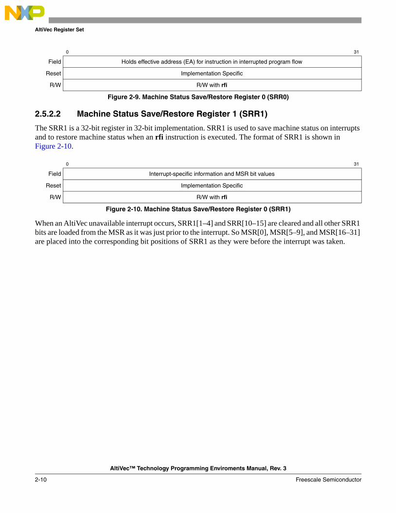
AltiVec Register Set
AltiVec™ Technology Programming Enviroments Manual, Rev. 3
2-10 Freescale Semiconductor
2.5.2.2 Machine Status Save/Restore Register 1 (SRR1)
The SRR1 is a 32-bit register in 32-bit implementation. SRR1 is used to save machine status on interrupts and to restore machine status when an rfi instruction is executed. The format of SRR1 is shown in Figure 2-10.
When an AltiVec unavailable interrupt occurs, SRR1[1–4] and SRR[10–15] are cleared and all other SRR1 bits are loaded from the MSR as it was just prior to the interrupt. So MSR[0], MSR[5–9], and MSR[16–31] are placed into the corresponding bit positions of SRR1 as they were before the interrupt was taken.
0 31
Field Holds effective address (EA) for instruction in interrupted program flow
Reset Implementation Specific
R/W R/W with rfi
Figure 2-9. Machine Status Save/Restore Register 0 (SRR0)
0 31
Field Interrupt-specific information and MSR bit values
Reset Implementation Specific
R/W R/W with rfi
Figure 2-10. Machine Status Save/Restore Register 0 (SRR1)

AltiVec™ Technology Programming Enviroments Manual, Rev. 3
Freescale Semiconductor 3-1
Chapter 3 Operand ConventionsThis chapter describes the operand conventions as they are represented in AltiVec technology at the user instruction set architecture (UISA) level. Detailed descriptions are provided of conventions used for transferring data between vector registers and memory, and representing data in these vector registers using both big- and little-endian byte ordering. Additionally, the floating-point default conditions for exceptions are described.
3.1 Data Organization in Memory In addition to supporting byte, half-word, and word operands, as defined in the PowerPC architecture UISA, AltiVec instruction set architecture (ISA) supports quad-word (128-bit) operands.
The following sections describe the concepts of alignment and byte ordering of data for quad words, otherwise alignment is the same as described in Chapter 3, “Operand Conventions,” in the Programming Environments Manual for 32-Bit Implementations of the PowerPC Architecture.
3.1.1 Aligned and Misaligned Accesses
Vectors are accessed from memory with instructions such as Vector Load Indexed (lvx) and Store Vector Indexed (stvx) instructions. The operand of a vector register to memory access instruction has a natural alignment boundary equal to the operand length. In other words, the natural address of an operand is an integral multiple of the operand length. A memory operand is said to be aligned if it is aligned at its natural boundary; otherwise it is misaligned. Each AltiVec instruction is a 4-byte word and is word-aligned like PowerPC instructions.
Operands for vector register to memory access instructions have the characteristics shown in Table 3-1.
The concept of alignment is also applied more generally to data in memory. For example, an 8-byte data item is said to be half-word aligned if its address is a multiple of 2; that is, the effective address (EA) points
Table 3-1. Memory Operand Alignment
Operand Length32-Bit Aligned
Address (28–31) 1
1 An x in an address bit position indicates that the bit can be 0 or 1 independent of the state of other bits in the address.
Byte 8 bits (1 byte) xxxx
Half-word 2 bytes xxx0
Word 4 bytes xx00
Quad word 16 bytes 0000

Operand Conventions
AltiVec™ Technology Programming Enviroments Manual, Rev. 3
3-2 Freescale Semiconductor
to the next effective address that is 2 bytes (a half-word) past the current effective address (EA + 2 bytes), and then the next being the EA + 4 bytes, and effective address would continue skipping every 2 bytes (2 bytes = 1 half-word). This ensures that the effective address is half-word aligned as it points to each successive half-word in memory.
It is important to understand that AltiVec memory operands are assumed to be aligned, and AltiVec memory accesses are performed as if the appropriate number of low-order bits of the specified effective address were zero. This assumption is different from PowerPC integer and floating-point memory access instructions where alignment is not always assumed. Thus, for AltiVec ISA, the low-order bit of the effective address is ignored for half-word AltiVec memory access instructions, and the low-order 4 bits of the effective address are ignored for quad-word AltiVec memory access instructions. The effect is to load or store the memory operand of the specified length that contains the byte addressed by the effective address.
If a memory operand is misaligned, additional instructions must be used to correctly place the operand in a vector register or in memory. AltiVec technology provides instructions to shift and merge the contents of two vector registers. These instructions facilitate copying misaligned quad-word operands between memory and the vector registers.
3.1.2 AltiVec Byte Ordering
For processors that implement the PowerPC architecture and AltiVec technology, the smallest addressable memory unit is the byte (8 bits), and scalars are composed of one or more sequential bytes. AltiVec ISA supports both big- and little-endian byte ordering. The default byte ordering is big-endian. However, the code sequence used to switch from big- to little-endian mode may differ among processors.
The PowerPC architecture uses the machine state register (MSR) for specifying byte ordering in little-endian mode (LE). A value of 0 specifies big-endian mode and a value of 1 specifies little-endian mode. For further details on byte ordering in the PowerPC architecture, refer to Chapter 3, “Operand Conventions,” in the Programming Environments Manual for 32-Bit Implementations of the PowerPC Architecture.
AltiVec ISA follows the endian support of the PowerPC architecture for elements up to double words with additional support for quad words. In AltiVec ISA when a 64-bit scalar is moved from a register to memory, it occupies 8 consecutive bytes in memory and a decision must be made regarding byte ordering in these 8 addresses.
3.1.2.1 Big-Endian Byte Ordering
For big-endian scalars, the most-significant byte (MSB) is stored at the lowest (or starting) address while the least-significant byte (LSB) is stored at the highest (or ending) address. This is called big-endian because the big end of the scalar comes first in memory.
3.1.2.2 Little-Endian Byte Ordering
For little-endian scalars, the LSB is stored at the lowest (or starting) address while the MSB is stored at the highest (or ending) address. This is called little-endian because the little end of the scalar comes first in memory.

Operand Conventions
AltiVec™ Technology Programming Enviroments Manual, Rev. 3
Freescale Semiconductor 3-3
3.1.3 Quad Word Byte Ordering Example
The idea of big- and little-endian byte ordering is best illustrated in an example of a quad word such as 0x0011_2233_4455_6677_8899_AABB_CCDD_EEFF located in memory. This quad word is used throughout this section to demonstrate how the bytes that comprise a quad word are mapped into memory.
The quad word (0x0011_2233_4455_6677_8899_AABB_CCDD_EEFF) is shown in big-endian mapping in Figure 3-1. A hexadecimal representation is used for showing address values and the values in the contents of each byte. The address is shown below each byte’s contents. The big-endian model addresses the quad word at address 0x00, which is the MSB (0x00), proceeding to the address 0x0F, which contains the LSB (0xFF).
Figure 3-2 shows the same quad word using little-endian mapping. In the little-endian model, the quad word’s 0x00 address specifies the LSB (0xFF) and proceeds to address 0x0F which contains its MSB (0x00).
Figure 3-2 shows the sequence of bytes laid out with addresses increasing from left to right. Programmers familiar with little-endian byte ordering may be more accustomed to viewing quad words laid out with addresses increasing from right to left, as shown in Figure 3-3.
This allows the little-endian programmer to view each scalar in its natural byte order of MSB to LSB. This section uses both conventions based on ease of understanding for the specific example.
Byte 0 1 2 3 4 5 6 7 8 9 10 11 12 13 14 15
Quad Word
Contents 00 11 22 33 44 55 66 77 88 99 AA BB CC DD EE FF
Address 00 01 02 03 04 05 06 07 08 09 0A 0B 0C 0D 0E 0F
↑MSB
↑LSB
Figure 3-1. Big-Endian Mapping of a Quad Word
Byte 0 1 2 3 4 5 6 7 8 9 10 11 12 13 14 15
Quad Word
Contents FF EE DD CC BB AA 99 88 77 66 55 44 33 22 11 00
Address 00 01 02 03 04 05 06 07 08 09 0A 0B 0C 0D 0E 0F
↑LSB
↑MSB
Figure 3-2. Little-Endian Mapping of a Quad Word
Byte 0 1 2 3 4 5 6 7 8 9 10 11 12 13 14 15
Quad Word
Contents 00 11 22 33 44 55 66 77 88 99 AA BB CC DD EE FF
Address 0F 0E 0D 0C 0B 0A 09 08 07 06 05 04 03 02 01 00
↑MSB
↑LSB
Figure 3-3. Little-Endian Mapping of a Quad Word—Alternate View
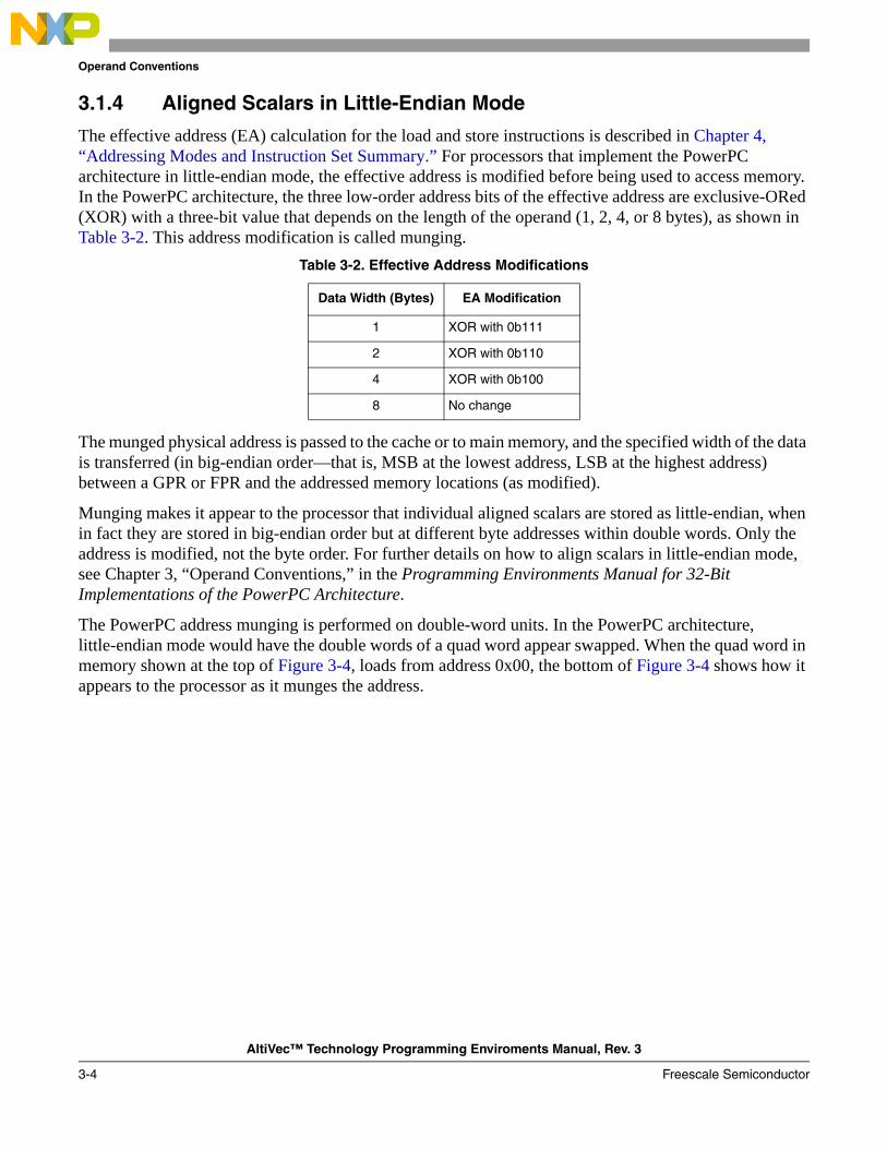
Operand Conventions
AltiVec™ Technology Programming Enviroments Manual, Rev. 3
3-4 Freescale Semiconductor
3.1.4 Aligned Scalars in Little-Endian Mode
The effective address (EA) calculation for the load and store instructions is described in Chapter 4, “Addressing Modes and Instruction Set Summary.” For processors that implement the PowerPC architecture in little-endian mode, the effective address is modified before being used to access memory. In the PowerPC architecture, the three low-order address bits of the effective address are exclusive-ORed (XOR) with a three-bit value that depends on the length of the operand (1, 2, 4, or 8 bytes), as shown in Table 3-2. This address modification is called munging.
The munged physical address is passed to the cache or to main memory, and the specified width of the data is transferred (in big-endian order—that is, MSB at the lowest address, LSB at the highest address) between a GPR or FPR and the addressed memory locations (as modified).
Munging makes it appear to the processor that individual aligned scalars are stored as little-endian, when in fact they are stored in big-endian order but at different byte addresses within double words. Only the address is modified, not the byte order. For further details on how to align scalars in little-endian mode, see Chapter 3, “Operand Conventions,” in the Programming Environments Manual for 32-Bit Implementations of the PowerPC Architecture.
The PowerPC address munging is performed on double-word units. In the PowerPC architecture, little-endian mode would have the double words of a quad word appear swapped. When the quad word in memory shown at the top of Figure 3-4, loads from address 0x00, the bottom of Figure 3-4 shows how it appears to the processor as it munges the address.
Table 3-2. Effective Address Modifications
Data Width (Bytes) EA Modification
1 XOR with 0b111
2 XOR with 0b110
4 XOR with 0b100
8 No change

Operand Conventions
AltiVec™ Technology Programming Enviroments Manual, Rev. 3
Freescale Semiconductor 3-5
Note that double words are swapped. The byte element addressed by the quad word’s base address, 0x0F, contains 0x28, while its MSB at address 0x00 contains 0x27. This is due to the PowerPC munging being applied to offsets within double words; AltiVec ISA requires a munge within quad words.
To accommodate the quad-word operands, the PowerPC architecture cannot simply be extended by munging an extra address bit. It would break existing code or platforms. Processors that implement AltiVec technology could not be mixed with non-AltiVec processors. Instead, AltiVec processors implement a double-word swap when moving quad words between vector registers and memory.
Figure 3-5 shows how this swapping could be implemented. This diagram represents the load path double-word swapping; the store path looks the same, except that the memory and internal boxes are reversed.
Figure 3-5. AltiVec Little-Endian Double-Word Swap
In the diagram, the numbers at the bottom of the byte boxes represent the offset address of that byte; the numbers at the top are the values of the bytes at that offset.The little-endian ordering is discontinuous because the PowerPC munging is performed only on double-word units. The purpose of the double-word swap within the AltiVec unit is to perform an additional swap that is not part of the PowerPC architecture.
When MSR[LE] = 1, double words are swapped and the bytes appear in their expected ordering. When MSR[LE] = 0, no swapping occurs.
Byte 0 1 2 3 4 5 6 7 8 9 10 11 12 13 14 15
Quad Word
Contents 20 21 22 23 24 25 26 27 28 29 2A 2B 2C 2D 2E 2F
Address 00 01 02 03 04 05 06 07 08 09 0A 0B 0C 0D 0E 0F
↑LSB
↑MSB
Byte 0 1 2 3 4 5 6 7 8 9 10 11 12 13 14 15
Quad Word
Contents 27 26 25 24 23 22 21 20 2F 2E 2D 2C 2B 2A 29 28
Address 00 01 02 03 04 05 06 07 08 09 0A 0B 0C 0D 0E 0F
Figure 3-4. Quad Word Load with PowerPC Munged Little-Endian Applied
00 01 02 03 04 05 06 07 08 09 0A 0B 0C 0D 0E 0F
27 26 25 24 23 22 21 20 2F 2E 2D 2C 2B 2A 29 28
0 1MSR[LE] 0 1MSR[LE]
00 01 02 03 04 05 06 07 08 09 0A 0B 0C 0D 0E 0F Memory Image
Internal ImageContentsAddress
ContentsAddress
2F 2E 2D 2C 2B 2A 29 28 27 26 25 24 23 22 21 202D

Operand Conventions
AltiVec™ Technology Programming Enviroments Manual, Rev. 3
3-6 Freescale Semiconductor
To summarize, in little-endian mode, the load vector element indexed instructions (lvebx, lvehx, and lvewx) and the store vector element indexed instructions (stvebx, stvehx, and stvewx) have the same 3-bit address munge applied to the memory address as is specified by the PowerPC architecture for integer and floating-point loads and stores. For the quad word load vector indexed instructions (lvx and lvxl) and the store vector indexed instructions (stvx, stvxl), the two double words of the quad-word scalar data are munged and swapped as they are moved between the vector register and memory.
3.1.5 Vector Register and Memory Access Alignment
When loading an aligned byte, half-word, or word memory operand into a vector register, the element that receives the data is the element that would have received the data had the entire aligned quad word containing the memory operand addressed by the effective address been loaded. Similarly, when an element in a vector register is stored into an aligned memory operand, the element selected to be stored is the element that would have been stored into the memory operand addressed by the effective address had the entire vector register been stored to the aligned quad word containing the memory operand addressed by the effective address. The position of the element in the target or source vector register depends on the endian mode, as described above. (Byte memory operands are always aligned.)
For aligned byte, half-word, and word memory operands, if the corresponding element number is known when the program is written, the appropriate vector splat and vector permute instructions can be used to copy or replicate the data contained in the memory operand after loading the operand into a vector register. Vector splat instructions will take the contents of an element in a vector register and replicates them into each element in the destination vector register. A vector permute instruction is the concatenation of the contents of two vectors. An example of this is given in detail in Section 3.1.6, “Quad-Word Data Alignment.” Another method is to replicate the element across an entire vector register before storing it into an arbitrary aligned memory operand of the same length; the replication ensures that the correct data is stored regardless of the offset of the memory operand in its aligned quad word in memory.
Because vector loads and stores are size-aligned, application binary interfaces (ABIs) should specify, and programmers should take care to align data on quad-word boundaries for maximum performance.
3.1.6 Quad-Word Data Alignment
AltiVec ISA does not provide for alignment interrupts for loading and storing data. When performing vector loads and stores, the effect is as if the low-order four bits of the address are 0x0, regardless of the actual effective address generated. Because vectors may often be misaligned due to the nature of the algorithm, AltiVec ISA provides support for post-alignment of quad-word loads and pre-alignment for quad-word stores. Note that in the following diagrams, the effect of the swapping described above is assumed and the memory diagrams will be shown with respect to the logical mapping of the data.
Figure 3-6 and Figure 3-7 show misaligned vectors in memory for both big- and little-endian ordering. The big-endian and little-endian examples assumes that the desired vector begins at address 0x03. In the figure, HI denotes high-order quad word, and LO means low-order quad word.

Operand Conventions
AltiVec™ Technology Programming Enviroments Manual, Rev. 3
Freescale Semiconductor 3-7
Figure 3-6 and Figure 3-7 show how such misaligned data causes data to be split across aligned quad words; only aligned quad words are loaded or stored by AltiVec load/store instructions. To align this vector, a program must load both (aligned) quad words that contain a portion of the misaligned vector data and then execute a Vector Permute (vperm) instruction to align the result.
3.1.6.1 Accessing a Misaligned Quad Word in Big-Endian Mode
Figure 3-1 shows the big-endian alignment model. Using the example in Figure 3-8, vHI and vLO represent vector registers that contain the misaligned quad words containing the MSBs and LSBs, respectively, of the misaligned quad word; vD is the target vector register.
Figure 3-8. Big-Endian Quad Word Alignment
Alignment is performed by left-rotating the combined 32-byte quantity (vHI:vLO) by an amount determined by the address of the first byte of the desired data. This left-rotation is done by means of a vperm instruction whose control vector is generated by a Load Vector for Shift Left (lvsl) instruction after loading the most-significant quad word (MSQ) and least-significant quad word (LSQ) that contain the desired vector. Note that a vector load is always safe to do if at least one byte in the vector is known to exist. The lvsl instruction uses the same address specification as the load vector indexed that loads the vHI component, which for big-endian ordering is the address of the desired vector.
Byte 0 1 2 3 4 5 6 7 8 9 10 11 12 13 14 15 16 17 18 19 20 21 22 23 24 25 26 27 28 29 30 31
Quad Word HI Quad Word LO
Contents 20 21 22 23 24 25 26 27 28 29 2A 2B 2C 2D 2E 2F
Address 00 01 02 03 04 05 06 07 08 09 0A 0B 0C 0D 0E 0F 10 11 12 13 14 15 16 17 18 19 1A 1B 1C 1D 1E 1F
↑MSB
↑LSB
Figure 3-6. Misaligned Vector in Big-Endian Mode
Byte 31 30 29 28 27 26 25 24 23 22 21 20 19 18 17 16 15 14 13 12 11 10 9 8 7 6 5 4 3 2 1 0
Quad Word HI Quad Word LO
Contents 2F 2E 2D 2C 2B 2A 29 28 27 26 25 24 23 22 21 20
Address 1F 1E 1D 1C 1B 1A 19 18 17 16 15 14 13 12 11 10 0F 0E 0D 0C 0B 0A 09 08 07 06 05 04 03 02 01 00
↑MSB
↑LSB
Figure 3-7. Misaligned Vector in Little-Endian Addressing Mode
10vHI
00
0F00
20 21 22 23 24 25 26 27 28 29 2A 2B 2C 2D 2E 2F
vLO
20 21 22 23 24 25 26 27 28 29 2A 2B 2C 2D 2E 2F
vD
0F 1F

Operand Conventions
AltiVec™ Technology Programming Enviroments Manual, Rev. 3
3-8 Freescale Semiconductor
The complete C code sequence for an unaligned load case is as follows:vector unsigned char vectorLoadUnaligned( vector unsigned char *where){
vector unsigned char permuteVector = vec_lvsl( 0,where ); vector unsigned char low = vec_ld( 0, where); vector unsigned char high = vec_ld( 15, where ); return vec_perm( low, high, permuteVector );
}
Note that when data streaming is used, the overhead of generating the alignment permute vector can be spread out and the latency of the loads may be absorbed by using loop unrolling.
The process of storing a misaligned vector is a bit different. It is possible to have data change in the process of storing two aligned vectors. To avoid a thread safety problem the data is stored using vector element stores.
The complete C code sequence for an unaligned store case is as follows:void StoreUnaligned( vector unsigned char v, unsigned char *where){
vector unsigned char tmp; tmp = vec_perm( v, v, vec_lvsr( 0, where) ); vec_ste( (vector unsigned char) tmp, 0, (unsigned char*) where);vec_ste( (vector unsigned short)tmp,1,(unsigned short*) where);vec_ste( (vector unsigned int) tmp, 3, (unsigned int*) where);vec_ste( (vector unsigned int) tmp, 4, (unsigned int*) where);vec_ste( (vector unsigned int) tmp, 8, (unsigned int*) where);vec_ste( (vector unsigned int) tmp, 12, (unsigned int*) where);vec_ste( (vector unsigned short)tmp,14,(unsigned short*) where);vec_ste( (vector unsigned char) tmp,15,(unsigned char*) where);
}
3.1.6.2 Accessing a Misaligned Quad Word in Little-Endian Mode
The instruction sequences used to access misaligned quad-word operands in little-endian mode are similar to those used in big-endian mode. The following instruction sequence can be used to load the misaligned quad word shown in Figure 3-7 into a vector register in little-endian mode. The load alignment case is shown in Figure 3-9. The vector register vHI and vLO receive the MSQ and LSQ, respectively; vD is the target vector register. The lvsr instruction uses the same address specification as an lvx that loads vLO; in little-endian byte ordering this is the address of the desired misaligned quad word.

Operand Conventions
AltiVec™ Technology Programming Enviroments Manual, Rev. 3
Freescale Semiconductor 3-9
lvx vLO,rA,rB # load the LSQ
lvsr vP,rA,rB # set the permute vector
addi rB,rB,15 # address of MSQ
lvx vHI,rA,rB # load MSQ component
vperm vD,vHI,vLO,vP # align the data
Figure 3-9. Little-Endian Alignment
3.1.6.3 Scalar Loads and Stores
No alignment is performed for scalar load or store instructions in AltiVec ISA. If a vector load or store address is not properly size aligned, the suitable number of least significant bits are ignored and a size aligned transfer occurs instead. Data alignment must be performed explicitly after being brought into the registers. No assistance is provided for aligning individual scalar elements that are not aligned on their natural boundary. The placement of scalar data in a vector element depends upon its address. That is, the placement of the addressed scalar is the same as if a load vector indexed instruction has been performed, except that only the addressed scalar is accessed (for cache-inhibited space); the values in the other vector elements are boundedly undefined. Also, data in the specified scalar is the same as if a store vector indexed instruction had been performed, except that only the scalar addressed is affected. No instructions are provided to assist in aligning individual scalar elements that are not aligned on their natural size boundary.
When a program knows the location of a scalar, it can perform the correct vector splats and vector permutes to move data to where it is required. For example, if a scalar is to be used as a source for a vector multiply (that is, each element multiplied by the same value), the scalar must be splatted into a vector register. Likewise, a scalar stored to an arbitrary memory location must be splatted into a vector register, and that register must be specified as the source of the store. This guarantees that the data appears in all possible positions of that scalar size for the store.
3.1.6.4 Misaligned Scalar Loads and Stores
Although no direct support of misaligned scalars is provided, the load-aligning sequence for big-endian vectors described in Section 3.1.6.1, “Accessing a Misaligned Quad Word in Big-Endian Mode,” can be used to position the scalar to the left vector element, which can then be used as the source for a splat. That is, the address of a scalar is also the address of the left-most element of the quad word at that address. Similarly, the read-modify-write sequences, with the mask adjusted for the scalar size, can be used to store misaligned scalars. The same is true for little-endian mode, the load-aligning sequence for little-endian vectors described Section 3.1.6.2, “Accessing a Misaligned Quad Word in Little-Endian Mode,” can be used to position the scalar to the right vector element, which can then be used as the source for a splat. That is, the address of a scalar is also the address of the right-most element of the quad word at that address.
0FvHI
1F
0F 00
2122232425262728292A2C2D2E2F
vLO
2F 2E 2D 2C 2B 2A 29 28 27 26 25 24 22 21 20
vD
0010
23
202B

Operand Conventions
AltiVec™ Technology Programming Enviroments Manual, Rev. 3
3-10 Freescale Semiconductor
Note that while these sequences work in cache-inhibited space, the physical accesses are not guaranteed to be atomic.
3.1.7 Mixed-Endian Systems
In many systems, the memory model is not as simple as the examples in this chapter. In particular, big-endian systems with subordinate little-endian buses (such as PCI) comprise a mixed-endian environment.
The basic mechanism to handle this is to use the Vector Permute (vperm) instruction to swap bytes within data elements. The value of the permute control vector depends on the size of the elements (8, 16, 32). That is, the permute control vector performs a parallel equivalent of the Load Word Byte-Reverse Indexed (lwbrx) PowerPC instruction within the vector registers.
The ultimate problem occurs when there are misaligned, mixed-endian vectors. This can be handled by applying a vector permute of the data as required for the misaligned case, followed by the swapping vector permute on that result. Note that for streaming cases, the effect of this double permute can be accomplished by computing the swapping permute of the alignment permute vector and then applying the resulting permute control vector to incoming data.
3.2 AltiVec Floating-Point Instructions—UISAThere are two kinds of floating-point instructions defined for the PowerPC ISA and AltiVec ISA:
• Computational • Noncomputational
Computational instructions are defined by the IEEE-754 standard for 32-bit arithmetic (those that perform addition, subtraction, multiplication, and division) and the multiply-add defined by the architecture. Noncomputational floating-point instructions consist of the floating-point load and store instructions. Only the computational instructions are considered floating-point operations throughout this chapter.
The single-precision format, value representations, and computational model to be defined in Chapter 3, “Operand Conventions,” in the Programming Environments Manual for 32-Bit Implementations of the PowerPC Architecture, apply to AltiVec floating-point except as follows:
• In general, no status bits are set to reflect the results of floating-point operations. The only exception is that VSCR[SAT] may be set by the Vector Convert to Fixed-Point Word instructions.
• With the exception of the two Vector Convert to Fixed-Point Word (vctuxs, vctsxs) instructions and three of the four Vector Round to Floating-Point Integer (vrfiz, vrfip, vrfim) instructions, all AltiVec floating-point instructions that round use the round-to-nearest rounding mode.
• Floating-point exceptions cannot cause the system error handler to be invoked.
If a function is required that is specified by the IEEE standard, is not supported by AltiVec ISA, and cannot be emulated satisfactorily using the functions that are supported by AltiVec ISA, the functions provided by the floating-point processor should be used; see Chapter 4, “Addressing Modes and Instruction Set Summary,” in the Programming Environments Manual for 32-Bit Implementations of the PowerPC Architecture.

Operand Conventions
AltiVec™ Technology Programming Enviroments Manual, Rev. 3
Freescale Semiconductor 3-11
3.2.1 Floating-Point Modes
AltiVec ISA supports two floating-point modes of operation—a Java mode and a non-Java mode of operation that is useful in circumstances where real-time performance is more important than strict Java and IEEE-standard compliance.
When VSCR[NJ] is 0 (default), operations are performed in Java mode. When VSCR[NJ] is 1, operations are carried out in the non-Java mode.
3.2.1.1 Java Mode
Java compliance requires compliance with only a subset of the Java/IEEE/C9X standard. The Java subset helps simplify floating-point implementations, as follows:
• Reducing the number of operations that must be supported• Eliminating exception status flags and traps• Producing results corresponding to all disabled exceptions, thus eliminating enabling control flags• Requiring only round-to-nearest rounding mode eliminates directed rounding modes and the
associated rounding control flags.
Java compliance requires the following aspects of the IEEE standard:• Supporting denorms as inputs and results (gradual underflow) for arithmetic operations• Providing NaN results for invalid operations• NaNs compare unordered with respect to everything, so that the result of any comparison of any
NaN to any data type is always false.
In some implementations, floating-point operations in Java mode may have somewhat longer latency on normal operands and possibly much longer latency on denormalized operands than operations in non-Java mode. This means that in Java mode overall real-time response may be somewhat worse and deadline scheduling may be subject to much larger variance than non-Java mode.
3.2.1.2 Non-Java Mode
In the non-Java/non-IEEE/non-C9X mode (VSCR[NJ] = 1), gradual underflow is not performed. Instead, any instruction that would have produced a denormalized result in Java mode substitutes a correctly signed zero (±0.0) as the final result. Also, denormalized input operands are flushed to the correctly signed zero (±0.0) before being used by the instruction.
The intent of this mode is to give programmers a way to assure optimum, data-insensitive, real-time response across implementations. Another way to improved response time would be to implement denormalized operations through software emulation.
It is architecturally permitted, but strongly discouraged, for an implementation to implement only non-Java mode. In such an implementation, the VSCR[NJ] does not respond to attempts to clear it and is always read back as a 1.
No other architecturally visible, implementation-specific deviations from this specification are permitted in either mode.

Operand Conventions
AltiVec™ Technology Programming Enviroments Manual, Rev. 3
3-12 Freescale Semiconductor
3.2.2 Floating-Point Infinities
Valid operations on infinities are processed according to the IEEE standard.
3.2.3 Floating-Point Rounding
All AltiVec floating-point arithmetic instructions use the IEEE default rounding mode, round-to-nearest. The IEEE directed rounding modes are not provided.
3.2.4 Floating-Point Exceptions
The following floating-point exceptions may occur during execution of AltiVec floating-point instructions.
• NaN operand exception• Invalid operation exception• Zero divide exception• Log of zero exception• Overflow exception• Underflow exception
If an exception occurs, a result is placed into the corresponding target element as described in the following subsections. This result is the default result specified by Java, the IEEE standard, or C9X, as applicable. Recall that denormalized source values are treated as if they were zero when VSCR[NJ] =1. The consequences regarding exceptions are as follows:
• Exceptions that can be caused by a zero source value can be caused by a denormalized source value when VSCR[NJ] = 1.
• Exceptions that can be caused by a nonzero source value cannot be caused by a denormalized source value when VSCR[NJ] = 1.
3.2.4.1 NaN Operand Exception
If the exponent of a floating-point number is 255 and the fraction is non-zero, then the value is a NaN. If the most significant bit of the fraction field of a NaN is zero, then the value is a signaling NaN (SNaN), otherwise it is a quiet NaN (QNaN). In all cases the sign of a NaN is irrelevant.
A NaN operand exception occurs when a source value for any of the following instructions is a NaN:• An AltiVec instruction that would normally produce floating-point results• Either of the two, Vector Convert to Unsigned Fixed-Point Word Saturate (vctuxs) or Vector
Convert to Signed Fixed-Point Word Saturate (vctsxs) instructions• Any of the four vector floating-point compare instructions.
The following actions can be taken:• If the AltiVec instruction would normally produce floating-point results, the corresponding result
is a source NaN selected as follows. In all cases, if the selected source NaN is an SNaN, it is

Operand Conventions
AltiVec™ Technology Programming Enviroments Manual, Rev. 3
Freescale Semiconductor 3-13
converted to the corresponding QNaN (by setting the high-order bit of the fraction field to 1 before being placed into the target element).
if the element in register vA is a NaN
then the result is that NaN
else if the element in register vB is a NaN
then the result is that NaN
else if the element in register vC is a NaN
then the result is that NaN
• If the instruction is either of the two vector convert to fixed-point word instructions (vctuxs, vctsxs), the corresponding result is 0x0000_0000. VSCR[SAT] is not affected.
• If the instruction is Vector Compare Bounds Floating-Point (vcmpbfp[.]), the corresponding result is 0xC000_0000.
• If the instruction is one of the other three vector floating-point compare instructions (vcmpeqfp[.], vcmpfgefp[.], vcmpbfp[.]), the corresponding result is 0x0000_0000.
3.2.4.2 Invalid Operation Exception
An invalid operation exception occurs when a source value is invalid for the specified operation. The invalid operations are as follows:
• Magnitude subtraction of infinities• Multiplication of infinity by zero• Vector Reciprocal Square Root Estimate Float (vrsqrtefp) of a negative, nonzero number or –X• Log base 2 estimate (vlogefp) of a negative, nonzero number or –X
The corresponding result is the QNaN 0x7FC0_0000. This is the single-precision format analogy of the double precision format generated QNaN described in Chapter 3, “Operand Conventions,” in the Programming Environments Manual for 32-Bit Implementations of the PowerPC Architecture.
3.2.4.3 Zero Divide Exception
A zero divide exception occurs when a Vector Reciprocal Estimate Floating-Point (vrefp) or Vector Reciprocal Square Root Estimate Floating-Point (vrsqrtefp) instruction is executed with a source value of zero.
The corresponding result is infinity, where the sign is the sign of the source value, as follows:• 1/+0.0 → +∞• 1/–0.0 → –∞••
1 +0.0( )⁄ +∞→
1 0.0–( )⁄ ∞–→

Operand Conventions
AltiVec™ Technology Programming Enviroments Manual, Rev. 3
3-14 Freescale Semiconductor
3.2.4.4 Log of Zero Exception
A log of zero exception occurs when a Vector Log Base 2 Estimate Floating-Point instruction (vlogefp) is executed with a source value of zero. The corresponding result is infinity. The exception cases are as follows:
• vlogefp log2(±0.0) → –∞• vlogefp log2(–x) → QNaN, where x ≠ 0
3.2.4.5 Overflow Exception
An overflow exception happens when either of the following conditions occurs:• For an AltiVec instruction that would normally produce floating-point results, the magnitude of
what would have been the result if the exponent range were unbounded exceeds that of the largest finite single-precision number.
• For either of the two Vector Convert To Fixed-Point Word instructions (vctuxs, vctsxs), either a source value is an infinity or the product of a source value and 2 unsigned immediate value (UIMM) is a number too large to be represented in the target integer format.
The following actions can be taken:• If the AltiVec instruction would normally produce floating-point results, the corresponding result
is infinity, where the sign is the sign of the intermediate result.• If the instruction is Vector Convert to Unsigned Fixed-Point Word Saturate (vctuxs), the
corresponding result is 0xFFFF_FFFF if the source value is a positive number or +X, and is 0x0000_0000 if the source value is a negative number or –X. VSCR[SAT] is set.
• If the instruction is Vector Convert to Signed Fixed-Point Word Saturate (vcfsx), the corresponding result is 0x7FFF_FFFF if the source value is a positive number or +X, and is 0x8000_0000 if the source value is a negative number or –X. VSCR[SAT] is set.
3.2.4.6 Underflow Exception
Underflow exceptions occur only for AltiVec instructions that would normally produce floating-point results. Underflow is detected before rounding. Underflow occurs when a nonzero intermediate result, computed as though both the precision and the exponent range were unbounded, is less in magnitude than the smallest normalized single-precision number (2–126).
The following actions can be taken:• If VSCR[NJ] = 0, the corresponding result is the value produced by denormalizing and rounding
the intermediate result.• If VSCR[NJ] = 1, the corresponding result is a zero, where the sign is the sign of the intermediate
result.

Operand Conventions
AltiVec™ Technology Programming Enviroments Manual, Rev. 3
Freescale Semiconductor 3-15
3.2.5 Floating-Point NaNs
The AltiVec floating-point data format is compliant with the Java/IEEE/C9X single-precision format. A quantity in this format can represent a signed normalized number, a signed denormalized number, a signed zero, a signed infinity, a quiet not a number (QNaN), or a signaling NaN (SNaN).
3.2.5.1 NaN Precedence
Whenever only one source operand of an instruction that returns a floating-point result is a NaN, then that NaN is selected as the input NaN to the instruction. When more than one source operand is a NaN, the precedence order for selecting the NaN is first from vA then from vB and then from vC. If the selected NaN is an SNaN, it is processed as described in Section 3.2.5.2, “SNaN Arithmetic.” QNaNs, are processed according to Section 3.2.5.3, “QNaN Arithmetic.”
3.2.5.2 SNaN Arithmetic
Whenever the input NaN to an instruction is an SNaN, a QNaN is delivered as the result, as specified by the IEEE standard when no trap occurs. The delivered QNaN is an exact copy of the original SNaN except that it is quieted; that is, the most-significant bit (msb) of the fraction is a one.
3.2.5.3 QNaN Arithmetic
Whenever the input NaN to an instruction is a QNaN, it is propagated as the result according to the IEEE standard. All information in the QNaN is preserved through all arithmetic operations.
3.2.5.4 NaN Conversion to Integer
All NaNs convert to zero on conversions to integer instructions such as vctuxs and vctsxs.
3.2.5.5 NaN Production
Whenever the result of an AltiVec operation is a NaN (for example, an invalid operation), the NaN produced is a QNaN with the sign bit = 0, exponent field = 255, msb of the fraction field = 1, and all other bits = 0.

Operand Conventions
AltiVec™ Technology Programming Enviroments Manual, Rev. 3
3-16 Freescale Semiconductor

AltiVec™ Technology Programming Enviroments Manual, Rev. 3
Freescale Semiconductor 4-1
Chapter 4 Addressing Modes and Instruction Set SummaryThis chapter describes instructions and addressing modes defined by AltiVec instruction set architecture (ISA) and according to the levels used by PowerPC architecture—user instruction set architecture (UISA) and virtual environment architecture (VEA). AltiVec instructions are primarily UISA; if otherwise, they are noted in the chapter. These instructions are divided into the following categories:
• Vector integer arithmetic instructions—These include arithmetic, logical, compare, rotate, and shift instructions, described in Section 4.2.1, “Vector Integer Instructions.”
• Vector floating-point arithmetic instructions—These include floating-point arithmetic instructions as well as a discussion on floating-point modes, described in Section 4.2.2, “Vector Floating-Point Instructions.”
• Vector load and store instructions—These include load and store instructions for vector registers, described in Section 4.2.3, “Load and Store Instructions.”
• Vector permutation and formatting instructions—These include pack, unpack, merge, splat, permute, select, and shift instructions, described in Section 4.2.5, “Vector Permutation and Formatting Instructions.”
• Processor control instructions—These instructions are used to read and write from the AltiVec Status and Control Register, described in Section 4.2.6, “Processor Control Instructions—UISA.”
• Memory control instructions—These instructions are used for managing caches (user level and supervisor level), described in Section 4.3.1, “Memory Control Instructions—VEA.”
This grouping of instructions does not necessarily indicate the execution unit that processes a particular instruction or group of instructions within a processor implementation.
AltiVec integer instructions operate on byte, half-word, and word operands. Floating-point instructions operate on single-precision operands. AltiVec ISA uses word-length instructions that are word-aligned. It provides for byte, half-word, and word operand fetches and stores between memory and the vector registers (VRs).
Arithmetic and logical instructions do not read or modify memory. To use the contents of a memory location in a computation for an arithmetic or logical instruction, the following steps are taken:
1. The memory contents must be loaded into a register with a load instruction. 2. The contents are then modified.3. The modified contents are written to the target location using a store instruction.
4.1 ConventionsThis section describes conventions used for the AltiVec instruction set. Descriptions of memory addressing, synchronization, and the AltiVec interrupt summary follow.

Addressing Modes and Instruction Set Summary
AltiVec™ Technology Programming Enviroments Manual, Rev. 3
4-2 Freescale Semiconductor
4.1.1 Execution Model
When used with PowerPC instructions, AltiVec instructions can be viewed as simply new PowerPC instructions that are freely intermixed with existing ones to provide additional functionality. Processors that implement the PowerPC architecture appear to execute instructions in program order. Some AltiVec implementations may not allow out-of-order execution and completion. Non-data dependent vector instructions may issue and execute while longer latency instructions issued previously are still in the execute stage. Register renaming avoids stalling dispatch on false dependencies and allows maximum register name reuse in heavily unrolled loops. The execution of a sequence of instructions will not be interrupted because the unit does not report IEEE exceptions, but rather produces the default results as specified in the Java/IEEE/C9X standards. The execution of a sequence of instructions may be interrupted only by a vector load or store instruction; otherwise, AltiVec instructions do not generate any interrupts.
4.1.2 Computation Modes
AltiVec ISA supports the PowerPC ISA. The AltiVec ISA supports the 32-bit implementation of the PowerPC architecture in that all registers except FPRs and VRs are 32 bits long and the effective addresses are 32 bits long.
This chapter describes only the instructions defined for 32-bit implementations of the PowerPC architecture.
4.1.3 Classes of Instructions
AltiVec instructions follow the illegal instruction class defined by PowerPC architecture in the section, “Classes of Instructions,” in Chapter 4, “Addressing Modes and Instruction Set Summary,” of the Programming Environments Manual for 32-Bit Implementations of the PowerPC Architecture. For AltiVec ISA, all unspecified encodings within the major opcode (04) that are not defined are illegal PowerPC instructions. The only exclusion in defining an unspecified encoding is an unused bit in an immediate field or specifier field (///).
4.1.4 Memory Addressing
A program references memory using the effective (logical) address computed by the processor when it executes a load, store, or cache instruction, and when it fetches the next sequential instruction.
4.1.4.1 Memory Operands
Bytes in memory are numbered consecutively starting with zero. Each number is the address of the corresponding byte.
Memory operands may be bytes, half-words, words, or quad words for AltiVec instructions. The address of a memory operand is the address of its first byte (that is, of its most significant bit (MSB)). Operand length is implicit for each instruction. AltiVec ISA supports both big- and little-endian byte ordering. The default byte and bit ordering is big-endian; see Section 3.1.2, “AltiVec Byte Ordering,” for more information.
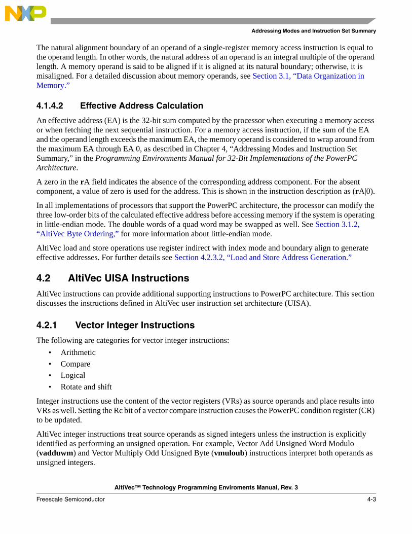
Addressing Modes and Instruction Set Summary
AltiVec™ Technology Programming Enviroments Manual, Rev. 3
Freescale Semiconductor 4-3
The natural alignment boundary of an operand of a single-register memory access instruction is equal to the operand length. In other words, the natural address of an operand is an integral multiple of the operand length. A memory operand is said to be aligned if it is aligned at its natural boundary; otherwise, it is misaligned. For a detailed discussion about memory operands, see Section 3.1, “Data Organization in Memory.”
4.1.4.2 Effective Address Calculation
An effective address (EA) is the 32-bit sum computed by the processor when executing a memory access or when fetching the next sequential instruction. For a memory access instruction, if the sum of the EA and the operand length exceeds the maximum EA, the memory operand is considered to wrap around from the maximum EA through EA 0, as described in Chapter 4, “Addressing Modes and Instruction Set Summary,” in the Programming Environments Manual for 32-Bit Implementations of the PowerPC Architecture.
A zero in the rA field indicates the absence of the corresponding address component. For the absent component, a value of zero is used for the address. This is shown in the instruction description as (rA|0).
In all implementations of processors that support the PowerPC architecture, the processor can modify the three low-order bits of the calculated effective address before accessing memory if the system is operating in little-endian mode. The double words of a quad word may be swapped as well. See Section 3.1.2, “AltiVec Byte Ordering,” for more information about little-endian mode.
AltiVec load and store operations use register indirect with index mode and boundary align to generate effective addresses. For further details see Section 4.2.3.2, “Load and Store Address Generation.”
4.2 AltiVec UISA InstructionsAltiVec instructions can provide additional supporting instructions to PowerPC architecture. This section discusses the instructions defined in AltiVec user instruction set architecture (UISA).
4.2.1 Vector Integer Instructions
The following are categories for vector integer instructions:• Arithmetic• Compare• Logical• Rotate and shift
Integer instructions use the content of the vector registers (VRs) as source operands and place results into VRs as well. Setting the Rc bit of a vector compare instruction causes the PowerPC condition register (CR) to be updated.
AltiVec integer instructions treat source operands as signed integers unless the instruction is explicitly identified as performing an unsigned operation. For example, Vector Add Unsigned Word Modulo (vadduwm) and Vector Multiply Odd Unsigned Byte (vmuloub) instructions interpret both operands as unsigned integers.
Addressing Modes and Instruction Set Summary
AltiVec™ Technology Programming Enviroments Manual, Rev. 3
4-4 Freescale Semiconductor
4.2.1.1 Saturation Detection
Most integer instructions have both signed and unsigned versions and many have both modulo (wrap-around) and saturating clamping modes. Saturation occurs whenever the result of a saturating instruction does not fit in the result field. Unsigned saturation clamps results to zero on underflow and to the maximum positive integer value (2n – 1, for example, 255 for byte fields) on overflow. Signed saturation clamps results to the smallest representable negative number (–2n–1, for example, –128 for byte fields) on underflow, and to the largest representable positive number (2n–1–1, for example, +127 for byte fields) on overflow. When a modulo instruction is used, the resultant number truncates overflow or underflow for the length (byte, half-word, word, quad word) and type of operand (unsigned, signed). The AltiVec ISA provides a way to detect saturation and sets the SAT bit in the Vector Status and Control Register (VSCR[SAT]) in a saturating instruction.
Borderline cases that generate results equal to saturation values, for example unsigned 0 + 0 → 0 and unsigned byte 1 + 254 → 255, are not considered saturation conditions and do not cause VSCR[SAT] to be set.
The VSCR[SAT] can be set by the following types of integer, floating-point, and formatting instructions: • Move to VSCR (mtvscr)• Vector add integer with saturation (vaddubs, vadduhs, vadduws, vaddsbs, vaddshs, vaddsws)• Vector subtract integer with saturation (vsububs, vsubuhs, vsubuws, vsubsbs, vsubshs, vsubsws)• Vector multiply-add integer with saturation (vmhaddshs, vmhraddshs)• Vector multiply-sum with saturation (vmsumuhs, vmsumshs, vsumsws)• Vector sum-across with saturation (vsumsws, vsum2sws, vsum4sbs, vsum4shs, vsum4ubs)• Vector pack with saturation (vpkuhus, vpkuwus, vpkshus, vpkswus, vpkshss, vpkswss)• Vector convert to fixed-point with saturation (vctuxs, vctsxs)
Note that only instructions that explicitly call for saturation can set VSCR[SAT]. Modulo integer instructions and floating-point arithmetic instructions never set VSCR[SAT]. For further details see Section 2.3.2, “Vector Status and Control Register (VSCR).”
4.2.1.2 Vector Integer Arithmetic Instructions
Table 4-1 lists the integer arithmetic instructions for processors that implement the PowerPC architecture.

Addressing Modes and Instruction Set Summary
AltiVec™ Technology Programming Enviroments Manual, Rev. 3
Freescale Semiconductor 4-5
Table 4-1. Vector Integer Arithmetic Instructions
Name Mnemonic Syntax Operation
Vector Add Unsigned
Integer [b,h,w] Modulo
vaddubmvadduhmvadduwm
vD,vA,vB
Places the sum (vA[unsigned integer elements]) + (vB[unsigned integer elements]) into vD[unsigned integer elements] using modulo arithmetic. For b, byte, integer length = 8 bits = 1 byte, add 16 unsigned integers from vA to the corresponding 16 unsigned integers from vB.For h, half-word, integer length =16 bits = 2 bytes, add 8 unsigned integers from vA to the corresponding 8 unsigned integers from vB.For w, word, integer length = 32 bits = 4 bytes, add 4 unsigned integers from vA to the corresponding 4 unsigned integers from vB.Note: unsigned or signed integers can be used with these instructions.
Vector Add Unsigned
Integer [b,h,w] Saturate
vaddubsvadduhsvadduws
vD,vA,vB
Place the sum (vA[unsigned integer elements]) + (vB[unsigned integer elements]) into vD[unsigned integer elements] using saturate clamping mode. Saturate clamping mode means if the resulting sum is >(2n–1) saturate to (2n–1), where n = b,h,w.For b, byte, integer length = 8 bits = 1 byte, add 16 unsigned integers from vA to the corresponding 16 unsigned integers from vB.For h, half-word, integer length = 16 bits = 2 bytes, add 8 unsigned integers from vA to the corresponding 8 unsigned integers formable.For w, word, integer length = 32 bits = 4 bytes, add 4 unsigned integers from vA to the corresponding 4 unsigned integers from vB.If the result saturates, VSCR[SAT] is set.
Vector Add Signed
Integer[b,h,w] Saturate
vaddsbsvaddshsvddsws
vD,vA,vB
Place the sum (vA[signed integer elements]) + (vB[signed integer elements]) into vD[signed integer elements] using saturate clamping mode. Saturate clamping mode means:if the sum is >(2n–1–1) saturate to (2n–1–1), andif < (–2n–1) saturate to (–2n–1), where n = b,h,w.For b, byte, integer length = 8 bits = 1 byte, add 16 signed integers from vA to the corresponding 16 signed integers from vB.For h, half-word, integer length = 16 bits = 2 bytes, add 8 signed integers from vA to the corresponding 8 signed integers from vB.For w, word, integer length = 32 bits = 4 bytes, add 4 signed integers from vA to the corresponding 4 signed integers from vB.If the result saturates, VSCR[SAT] is set.
Vector Add and Write Carry-Out Unsigned
Word
vaddcuw vD,vA,vB
Take the carry out of summing (vA) + (vB) and place it into vD.For w, word, integer length = 32 bits = 4 bytes, add 4 unsigned integers from vA to the corresponding 4 unsigned integers from vB and the resulting carry outs are correspondingly placed in vD.
Vector Subtract Unsigned
Integer Modulo[b,h,w]
vsububmvsubuhmvsubuwm
vD,vA,vB
Place the unsigned integer sum (vA) – (vB) into vD using modulo arithmetic.For b, byte, integer length = 8 bits =1 byte, subtract 16 unsigned integers in vB from the corresponding 16 unsigned integers in vA.For h, half-word, integer length = 16 bits = 2 bytes, subtract 8 unsigned integers in vB from the corresponding 8 unsigned integers in vA.For w, word, integer length = 32 bits = 4 bytes, subtract 4 unsigned integers in vB from the corresponding 4 unsigned integers in vA.Note that unsigned or signed integers can be used with these instructions.

Addressing Modes and Instruction Set Summary
AltiVec™ Technology Programming Enviroments Manual, Rev. 3
4-6 Freescale Semiconductor
Vector Subtract Unsigned
Integer Saturate [b,h,w]
vsububsvsubuhsvsubuws
vD,vA,vB
Place the unsigned integer sum vA – vB into vD using saturate clamping mode, that is, if the sum <0, it saturates to 0 corresponding to b,h,w.For b, byte, integer length = 8 bits = 1 byte, subtract 16 unsigned integers in vB from the corresponding 16 unsigned integers in vA.For h, half-word, integer length =16 bits = 2 bytes, subtract 8 unsigned integers in vB from the corresponding 8 unsigned integers in vA.For w, word, integer length = 32 bits = 4 bytes, subtract 4 unsigned integers in vB from the corresponding 4 unsigned integers in vA.If the result saturates, VSCR[SAT] is set.
Vector Subtract
Signed Integer Saturate[b,h,w]
vsubsbsvsubshsvsubsws
vD,vA,vB
Place the signed integer sum (vA) – (vB) into vD using saturate clamping mode. Saturate clamping mode means:if the sum is >(2n-1–1) saturate to (2n–1–1) andif < (–2n–1) saturate to (–2n–1), where n = b,h,w.For b, byte, integer length = 8 bits = 1 byte, subtract 16 signed integers in vB from the corresponding sixteen signed integers in vA.For h, half-word, integer length = 16 bits = 2 bytes, subtract 8 signed integers in vB from the corresponding 8 signed integers in vA.For w, word, integer length = 32 bits = 4 bytes, subtract 4 signed integers in vB from the corresponding 4 signed integers in vA.
Vector Subtract and
Write Carry-Out Unsigned
Word
vsubcuw vD,vA,vB
Take the carry out of the sum (vA) – (vB) and place it into vD.For w, word, integer length = 32 bits = 4 bytes, subtract 4 unsigned integers in vB from the corresponding 4 unsigned integers in vA and place the resulting carry outs into vD.
Vector Multiply Odd Unsigned Integer [b,h]
Modulo
vmuloubvmulouh
vD,vA,vB
Place the unsigned integer products of (vA) * (vB) into vD using modulo arithmetic mode.For b, byte, integer length = 8 bits =1 byte, multiply 8 odd-numbered unsigned integer byte elements from vA to the corresponding 8 odd-numbered unsigned integer byte elements from vB resulting in 8 unsigned integer half-word products in vD.For h, half-word, integer length =16 bits = 2 bytes, multiply 4 odd-numbered unsigned integer half-word elements from vA to the corresponding 4 odd numbered unsigned integer half-word elements from vB resulting in 4 unsigned integer word products in vD.
Vector Multiply Odd Signed Integer [b,h]
Modulo
vmulosbvmulosh
vD,vA,vB
Place the signed integer product of (vA) * (vB) into vD using modulo arithmetic mode.For b, byte, integer length = 8 bits = 1 byte, multiply 8 odd-numbered signed integer byte elements from vA to 8 odd-numbered signed integer byte elements from vB resulting in 8 signed integer half-word products in vD.For h, half-word, integer length = 16 bits = 2 bytes, multiply 4 odd-numbered signed integer half-word elements from vA to 4 odd-numbered signed integer half-word elements from vB resulting in 4 signed integer word products in vD.
Table 4-1. Vector Integer Arithmetic Instructions (continued)
Name Mnemonic Syntax Operation

Addressing Modes and Instruction Set Summary
AltiVec™ Technology Programming Enviroments Manual, Rev. 3
Freescale Semiconductor 4-7
Vector Multiply Even
Unsigned Integer [b,h]
Modulo
vmuleubvmuleuh
vD,vA,vB
Place the unsigned integer products of (vA) * (vB) into vD using modulo arithmetic mode.For b, byte, integer length = 8 bits =1 byte, multiply 8 even-numbered unsigned integer byte elements from vA to 8 even-numbered unsigned integer byte elements from vB resulting in 8 unsigned integer half-word products in vD.For h, half-word, integer length = 16 bits = 2 bytes, multiply 4 even-numbered unsigned integer half-word elements from vA to 4 even-numbered unsigned integer half-word elements from vB resulting in 4 unsigned integer word products in vD.
Vector Multiply Even Signed Integer [b,h]
Modulo
vmulesbvmulesh
vD,vA,vB
Place the signed integer product of (vA) * (vB) into vD using modulo arithmetic mode.For b, byte, integer length = 8 bits = 1 byte, multiply 8 even-numbered signed integer byte elements from vA to 8 even-numbered signed integer byte elements from vB resulting in 8 signed integer half-word products in vD.For h, half-word, integer length = 16 bits = 2 bytes, multiply 4 even-numbered signed integer half-word elements from vA to 4 even-numbered signed integer half-word elements from vB resulting in 4 signed integer word products in vD.
Vector Multiply-High
and Add Signed
Half-Word Saturate
vmhaddshs vD,vA,vB,vC
The 17 most significant bits (msb’s)of the product of (vA) * (vB) adds to sign-extended vC and places the result into vD.For h, half-word, integer length = 16 bits = 2 bytes, multiply the 8 signed half-words from vA with the corresponding 8 signed half-words from vB to produce a 32-bit intermediate product and then take the 17 msbs (bits 0–16) of the 8 intermediate products and add them to the 8 sign-extended half-words in vC, place the 8 half-word saturated results in vD. If the intermediate product is as follows:> (215–1) saturate to (215–1) and if< –215 saturate to –215.If the results saturates, VSCR[SAT] is set.
Vector Multiply-High Round and Add Signed Half-Word Saturate
vmhraddshs vD,vA,vB,vC
Add the rounded product of (vA) * (vB) to sign-extended vC and place the result into vD.For h, half-word, integer length = 16 bits = 2 bytes, multiply the eight signed integers from vA to the corresponding eight signed integers from vB and then round the 8 immediate products by adding the value 0x0000_4000 to it. Then add the most significant bits (msb), bits 0–16, of the 8 rounded immediate products to the 8 sign-extended values in vC and place the eight signed half-word saturated results into vD. If the intermediate product is:> (215–1) saturate to (215–1), or if< –215 saturate to –215.If the result saturates, VSCR[SAT] is set.
Vector Multiply-Low
and Add Unsigned Half-Word
Modulo
vmladduhm vD,vA,vB,vC
Add the product of (vA) * (vB) to zero-extended vC and place into vD.For h, half-word, integer length =16 bits = 2 bytes, multiply the 8 signed integers from vA to the corresponding 8 signed integers from vB to produce a 32-bit intermediate product. The 16-bit value in vC is zero-extended to 32 bits and added to the intermediate product and the lower 16 bits of the sum (bit 16–31) is placed in vD.Note that unsigned or signed integers can be used with these instructions.
Table 4-1. Vector Integer Arithmetic Instructions (continued)
Name Mnemonic Syntax Operation
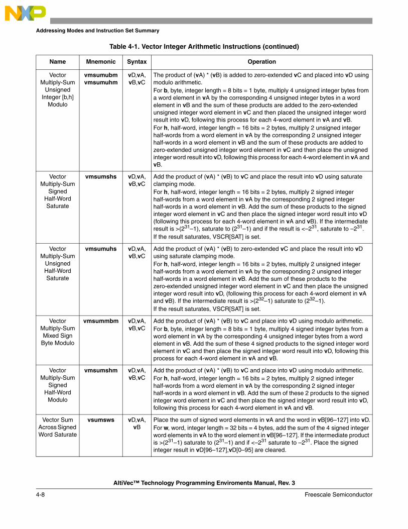
Addressing Modes and Instruction Set Summary
AltiVec™ Technology Programming Enviroments Manual, Rev. 3
4-8 Freescale Semiconductor
Vector Multiply-Sum
Unsigned Integer [b,h]
Modulo
vmsumubmvmsumuhm
vD,vA,vB,vC
The product of (vA) * (vB) is added to zero-extended vC and placed into vD using modulo arithmetic.For b, byte, integer length = 8 bits = 1 byte, multiply 4 unsigned integer bytes from a word element in vA by the corresponding 4 unsigned integer bytes in a word element in vB and the sum of these products are added to the zero-extended unsigned integer word element in vC and then placed the unsigned integer word result into vD, following this process for each 4-word element in vA and vB.For h, half-word, integer length = 16 bits = 2 bytes, multiply 2 unsigned integer half-words from a word element in vA by the corresponding 2 unsigned integer half-words in a word element in vB and the sum of these products are added to zero-extended unsigned integer word element in vC and then place the unsigned integer word result into vD, following this process for each 4-word element in vA and vB.
Vector Multiply-Sum
Signed Half-Word Saturate
vmsumshs vD,vA,vB,vC
Add the product of (vA) * (vB) to vC and place the result into vD using saturate clamping mode.For h, half-word, integer length = 16 bits = 2 bytes, multiply 2 signed integer half-words from a word element in vA by the corresponding 2 signed integer half-words in a word element in vB. Add the sum of these products to the signed integer word element in vC and then place the signed integer word result into vD (following this process for each 4-word element in vA and vB). If the intermediate result is >(231–1), saturate to (231–1) and if the result is <–231, saturate to –231.If the result saturates, VSCR[SAT] is set.
Vector Multiply-Sum
Unsigned Half-Word Saturate
vmsumuhs vD,vA,vB,vC
Add the product of (vA) * (vB) to zero-extended vC and place the result into vD using saturate clamping mode.For h, half-word, integer length = 16 bits = 2 bytes, multiply 2 unsigned integer half-words from a word element in vA by the corresponding 2 unsigned integer half-words in a word element in vB. Add the sum of these products to the zero-extended unsigned integer word element in vC and then place the unsigned integer word result into vD, (following this process for each 4-word element in vA and vB). If the intermediate result is >(232–1) saturate to (232–1).If the result saturates, VSCR[SAT] is set.
Vector Multiply-Sum Mixed Sign
Byte Modulo
vmsummbm vD,vA,vB,vC
Add the product of (vA) * (vB) to vC and place into vD using modulo arithmetic.For b, byte, integer length = 8 bits = 1 byte, multiply 4 signed integer bytes from a word element in vA by the corresponding 4 unsigned integer bytes from a word element in vB. Add the sum of these 4 signed products to the signed integer word element in vC and then place the signed integer word result into vD, following this process for each 4-word element in vA and vB.
Vector Multiply-Sum
Signed Half-Word
Modulo
vmsumshm vD,vA,vB,vC
Add the product of (vA) * (vB) to vC and place into vD using modulo arithmetic.For h, half-word, integer length = 16 bits = 2 bytes, multiply 2 signed integer half-words from a word element in vA by the corresponding 2 signed integer half-words in a word element in vB. Add the sum of these 2 products to the signed integer word element in vC and then place the signed integer word result into vD, following this process for each 4-word element in vA and vB.
Vector Sum Across Signed Word Saturate
vsumsws vD,vA,vB
Place the sum of signed word elements in vA and the word in vB[96–127] into vD.For w, word, integer length = 32 bits = 4 bytes, add the sum of the 4 signed integer word elements in vA to the word element in vB[96–127]. If the intermediate product is >(231–1) saturate to (231–1) and if <–231 saturate to –231. Place the signed integer result in vD[96–127],vD[0–95] are cleared.
Table 4-1. Vector Integer Arithmetic Instructions (continued)
Name Mnemonic Syntax Operation

Addressing Modes and Instruction Set Summary
AltiVec™ Technology Programming Enviroments Manual, Rev. 3
Freescale Semiconductor 4-9
Vector Sum Across Partial (1/2) Signed
Word Saturate
vsum2sws vD,vA,vB
Add vA[word 0 + word 1] + vB[word 1] and place in vD[word 1]. Repeat only add vA[word 2 + word 3] + vB[word 3] and place in vD[word 3].word 0 = bits 0–31word 1 = bits 32–63word 2 = bits 64–95word 3 = bits 96–127Figure 1-2 shows a picture of what the word elements would look like in a vector register.Add the sum of word 0 and word 1 of vA to word 1 of vB using saturate clamping mode and place the result is into word 1of vD. Then add the sum of word 2 and word 3 of (vA) to word 3 of vB using saturate clamping mode and place those results into word 3 in vD. If the intermediate result for either calculation is >(231–1) then saturate to (231–1) and if <–231 then saturate to –231.If the result saturates, VSCR[SAT] is set.
Vector Sum Across Partial (1/4) Unsigned Byte Saturate
vsum4ubs vD,vA,vB
Add vA[4 byte elements sum to a word] and vB[word element] then place in vD[word element] using saturate clamping mode.For b, byte, integer length = 8 bits = 1 byte, for each word element in vB, add the sum of 4 unsigned bytes in the word in vA to the unsigned word element in vB and then place the results into the corresponding unsigned word element in vD. If the intermediate result for is >(232–1) it saturates to (232–1).If the result saturates, VSCR[SAT] is set.
Vector Sum Across Partial (1/4) Signed
Integer Saturate
vsum4sbsvsum4shs
vD,vA,vB
Add vA[sum of signed integer elements in word] and vB[word element] then place in vD[word element] using saturate clamping mode.For b, byte, integer length = 8 bits = 1 byte, for each word element in vB, add the sum of 4 signed bytes in the word in vA to the signed word element in vB and then place the results into the corresponding signed word element in vD. If the intermediate result is > (231–1) then saturate to (231–1) and if <–231 then saturate to –231. For h, half-word, integer length = 16 bits = 2 bytes, for each word element in vB, add the sum of 2 signed half-words in the word in vA to the signed word element in vB and then place the results into the corresponding signed word element in vD. If the intermediate result is >(231–1) then saturate to (231–1) and if <–231 then saturate to –231. If the result saturates, VSCR[SAT] is set.
Vector Average
Unsigned Integer [b,h,w]
vavgubvavguhvavguw
vD,vA,vB
Add the sum of (vA[unsigned integer elements]+ vB[unsigned integer elements]) +1 and place into vD using modulo arithmetic.For b, byte, integer length = 8 bits = 1 byte, add 16 unsigned integers from vA to 16 unsigned integers from vB and then add 1 to the sums and place the high order result in vD.For h, half-word, integer length = 16 bits = 2 bytes, add 8 unsigned integers from vA to 8 unsigned integers from vB and then add 1 to the sums and place the high order result in vD.For w, word, integer length = 32 bits = 4 bytes, add 4 unsigned integers from vA to 4 unsigned integers from vB and then add 1 to the sums and place the high order result in vD.If the result saturates, VSCR[SAT] is set.
Table 4-1. Vector Integer Arithmetic Instructions (continued)
Name Mnemonic Syntax Operation

Addressing Modes and Instruction Set Summary
AltiVec™ Technology Programming Enviroments Manual, Rev. 3
4-10 Freescale Semiconductor
Vector Average
Signed Integer [b,h,w]
vavgsbvavgshvavgsw
vD,vA,vB
Add the sum of (vA[signed integer elements]+ vB[signed integer elements]) +1 and place into vD using modulo arithmetic.For b, byte, integer length = 8 bits = 1 byte, add 16 signed integers from vA to 16 signed integers from vB and then add 1 to the sums and place the high order result in vD.For h, half-word, integer length = 16 bits = 2 bytes, add 8 signed integers from vA to 8 signed integers from vB and then add 1 to the sums and place the high order result in vD.For w, word, integer length = 32 bits = 4 bytes, add 4 signed integers from vA to 4 signed integers from vB and then add 1 to the sums and place the high order result in vD.
Vector Maximum Unsigned
Integer [b,h,w]
vmaxubvmaxuhvmaxuw
vD,vA,vB
Compare the maximum of vA and vB unsigned integers for each integer value and which ever value is larger, place that unsigned integer value into vD.For b, byte, integer length = 8 bits = 1 byte, compare 16 unsigned integers from vA with 16 unsigned integers from vB.For h, half-word, integer length = 16 bits = 2 bytes, compare 8 unsigned integers from vA with 8 unsigned integers from vB.For w, word, integer length = 32 bits = 4 bytes, compare 4 unsigned integers from vA with 4 unsigned integers from vB.
Vector Maximum
Signed Integer [b,h,w]
vmaxsbvmaxshvmaxsw
vD,vA,vB
Compare the maximum of vA and vB signed integers for each integer value and which ever value is larger, place that signed integer value into vD.For b, byte, integer length = 8 bits =1 byte, compare 16 signed integers from vA with 16 signed integers from vB.For h, half-word, integer length =16 bits = 2 bytes, compare 8 signed integers from vA with 8 signed integers from vB.For w, word, integer length = 32 bits = 4 bytes, compare 8 signed integers from vA with 8 signed integers from vB.
Vector Minimum Unsigned
Integer [b,h,w]
vminubvminuhvminuw
vD,vA,vB
Compare the minimum of vA and vB unsigned integers for each integer value and which ever value is smaller, place that unsigned integer value into vD.For b, byte, integer length = 8 bits = 1 byte, compare 16 unsigned integers from vA with 16 unsigned integers from vB.For h, half-word, integer length = 16 bits = 2 bytes, compare 8 unsigned integers from vA with 8 unsigned integers from vB.For w, word, integer length = 32 bits = 4 bytes, compare 4 unsigned integers from vA with 4 unsigned integers from vB.
Vector Minimum
Signed Integer [b,h,w]
vminsbvminshvminsw
vD,vA,vB
Compare the minimum of vA and vB signed integers for each integer value and which ever value is smaller, place that signed integer value into vD.For b, byte, integer length = 8 bits = 1 byte, compare 16 signed integers from vA with 16 signed integers from vB.For h, half-word, integer length = 16 bits = 2 bytes, compare 8 signed integers from vA with 8 signed integers from vB.For w, word, integer length = 32 bits = 4 bytes, compare 4 signed integers from vA with 4 signed integers from vB.
Table 4-1. Vector Integer Arithmetic Instructions (continued)
Name Mnemonic Syntax Operation
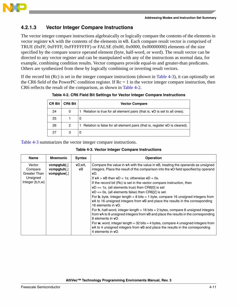
Addressing Modes and Instruction Set Summary
AltiVec™ Technology Programming Enviroments Manual, Rev. 3
Freescale Semiconductor 4-11
4.2.1.3 Vector Integer Compare Instructions
The vector integer compare instructions algebraically or logically compare the contents of the elements in vector register vA with the contents of the elements in vB. Each compare result vector is comprised of TRUE (0xFF, 0xFFFF, 0xFFFFFFFF) or FALSE (0x00, 0x0000, 0x00000000) elements of the size specified by the compare source operand element (byte, half-word, or word). The result vector can be directed to any vector register and can be manipulated with any of the instructions as normal data, for example, combining condition results. Vector compares provide equal-to and greater-than predicates. Others are synthesized from these by logically combining or inverting result vectors.
If the record bit (Rc) is set in the integer compare instructions (shown in Table 4-3), it can optionally set the CR6 field of the PowerPC condition register. If Rc = 1 in the vector integer compare instruction, then CR6 reflects the result of the comparison, as shown in Table 4-2.
Table 4-3 summarizes the vector integer compare instructions.
Table 4-2. CR6 Field Bit Settings for Vector Integer Compare Instructions
CR Bit CR6 Bit Vector Compare
24 0 1 Relation is true for all element pairs (that is, vD is set to all ones).
25 1 0
26 2 1 Relation is false for all element pairs (that is, register vD is cleared).
27 3 0
Table 4-3. Vector Integer Compare Instructions
Name Mnemonic Syntax Operation
Vector Compare
Greater Than Unsigned
Integer [b,h,w]
vcmpgtub[.]vcmpgtuh[.]vcmpgtuw[.]
vD,vA,vB
Compare the value in vA with the value in vB, treating the operands as unsigned integers. Place the result of the comparison into the vD field specified by operand vD.If vA > vB then vD = 1s; otherwise vD = 0s.If the record bit (Rc) is set in the vector compare instruction, then vD == 1s, (all elements true) then CR6[0] is setvD == 0s, (all elements false) then CR6[2] is set.For b, byte, integer length = 8 bits = 1 byte, compare 16 unsigned integers from vA to 16 unsigned integers from vB and place the results in the corresponding 16 elements in vD.For h, half-word, integer length = 16 bits = 2 bytes, compare 8 unsigned integers from vA to 8 unsigned integers from vB and place the results in the corresponding 8 elements in vD.For w, word, integer length = 32 bits = 4 bytes, compare 4 unsigned integers from vA to 4 unsigned integers from vB and place the results in the corresponding 4 elements in vD.

Addressing Modes and Instruction Set Summary
AltiVec™ Technology Programming Enviroments Manual, Rev. 3
4-12 Freescale Semiconductor
4.2.1.4 Vector Integer Logical Instructions
The vector integer logical instructions shown in Table 4-4 perform bit-parallel operations on the operands.
Vector Compare
Greater Than Signed Integer
[b,h,w]
vcmpgtsb[.]vcmpgtsh[.]vcmpgtsw[.]
vD,vA,vB
Compare the value in vA with the value in vB, treating the operands as signed integers. Place the result of the comparison into the vD field specified by operand vD.If vA > vB then vD =1s; otherwise vD = 0sIf the record bit (Rc) is set in the vector compare instruction, then vD == 1s, (all elements true) then CR6[0] is setvD == 0s, (all elements false) then CR6[2] is set.For b, byte, integer length = 8 bits = 1 byte, compare 16 signed integers from vA to 16 signed integers from vB and place the results in the 16 corresponding elements in vD.For h, half-word, integer length = 16 bits = 2 bytes, compare 8 signed integers from vA to 8 signed integers from vB and place the results in the 8 corresponding elements in vD.For w, word, integer length = 32 bits = 4 bytes, compare 4 signed integers from vA to 4 signed integers from vB and place the results in the 4 corresponding elements in vD.
Vector CompareEqual To Unsigned
Integer [b,h,w]
vcmpequb[.]vcmpequh[.]vcmpequw[.]
vD,vA,vB
Compare the value in vA with the value in vB, treating the operands as unsigned integers. Place the result of the comparison into the vD field specified by operand vD.If vA = vB then vD = 1s; otherwise vD = 0s.If the record bit (Rc) is set in the vector compare instruction then vD == 1s, (all elements true) then CR6[0] is setVD == 0s, (all elements false) then CR6[2] is set.For b, byte, integer length = 8 bits = 1 byte, compare 16 unsigned integers from vA to 16 unsigned integers from vB and place the results in the corresponding 16 elements in vD.For h, half-word, integer length = 16 bits = 2 bytes, compare 8 unsigned integers from vA to 8 unsigned integers from vB and place the results in the corresponding 8 elements in vD.For w, word, integer length = 32 bits = 4 bytes, compare 4 unsigned integers from vA to 4 unsigned integers from vB and place the results in the corresponding 4 elements in vD.Note: vcmpequb[.], vcmpequh[.], and vcmpequw[.] can use both unsigned and signed integers.
Table 4-4. Vector Integer Logical Instructions
Name Mnemonic Syntax Operation
Vector Logical AND vand vD,vA,vB AND the contents of vA with vB and place the result into vD.
Vector Logical OR vor vD,vA,vB OR the contents of vA with vB and place the result into vD.
Vector Logical XOR vxor vD,vA,vB XOR the contents of vA with vB and place the result into vD.
Vector Logical AND with Complement
vandc vD,vA,vB AND the contents of vA with the complement of vB and place the result into vD.
Vector Logical NOR vnor vD,vA,vB NOR the contents of vA with vB and place the result into vD.
Table 4-3. Vector Integer Compare Instructions (continued)
Name Mnemonic Syntax Operation

Addressing Modes and Instruction Set Summary
AltiVec™ Technology Programming Enviroments Manual, Rev. 3
Freescale Semiconductor 4-13
4.2.1.5 Vector Integer Rotate and Shift Instructions
The vector integer rotate instructions are summarized in Table 4-5.
The vector integer shift instructions are summarized in Table 4-6.
Table 4-5. Vector Integer Rotate Instructions
Name Mnemonic Syntax Operation
Vector Rotate Left Integer
[b,h,w]
vrlbvrlhvrlw
vD,vA,vB
Rotate each element in vA left by the number of bits specified in the low-order log2(n) bits of the corresponding element in vB. Place the result into the corresponding element of vD.For b, byte, integer length = 8 bits = 1 byte, use 16 integers from vA with 16 integers from vB.For h, half-word, integer length = 16 bits = 2 bytes, use 8 integers from vA with 8 integers from vB.For w, word, integer length = 32 bits = 4 bytes, use 4 integers from vA with 4 integers from vB.
Table 4-6. Vector Integer Shift Instructions
Name Mnemonic Syntax Operation
Vector Shift Left Integer
[b,h,w]
vslbvslhvslw
vD,vA,vB
Shift each element in vA left by the number of bits specified in the low-order log2(n) bits of the corresponding element in vB. If bits are shifted out of bit 0 of the element they are lost. Supply zeros to the vacated bits on the right. Place the result into the corresponding element of vD.For b, byte, integer length = 8 bits = 1 byte, use 16 integers from vA with 16 integers from vB.For h, half-word, integer length = 16 bits = 2 bytes, use 8 integers from vA with 8 integers from vB.For w, word, integer length = 32 bits = 4 bytes, use 4 integers from vA with 4 integers from vB.
Vector Shift Right Integer
[b,h,w]
vsrbvsrhvsrw
vD,vA,vB
Shift each element in vA right by the number of bits specified in the low-order log2(n) bits of the corresponding element in vB. If bits are shifted out of bit n–1 of the element they are lost. Supply zeros to the vacated bits on the left. Place the result into the corresponding element of vD.For b, byte, integer length = 8 bits = 1 byte, use 16 integers from vA with 16 integers from vB.For h, half-word, integer length = 16 bits = 2 bytes, use 8 integers from vA with 8 integers from vB.For w, word, integer length = 32 bits = 4 bytes, use 4 integers from vA with 4 integers from vB.
Vector Shift Right
Algebraic Integer [b,h,w]
vsrabvsrahvsraw
vD,vA,vB
Shift each element in vA right by the number of bits specified in the low-order log2(n) bits of the corresponding element in vB. If bits are shifted out of bit n–1 of the element they are lost. Replicate bit 0 of the element to fill the vacated bits on the left. Place the result into the corresponding element of vD. For b, byte, integer length = 8 bits = 1 byte, use 16 integers from vA with 16 integers from vB.For h, half-word, integer length = 16 bits = 2 bytes, use 8 integers from vA with 8 integers from vB.For w, word, integer length = 32 bits = 4 bytes, use 4 integers from vA with 4 integers from vB.

Addressing Modes and Instruction Set Summary
AltiVec™ Technology Programming Enviroments Manual, Rev. 3
4-14 Freescale Semiconductor
4.2.2 Vector Floating-Point Instructions
This section describes the vector floating-point instructions, which include the following:• Arithmetic • Rounding and conversion• Compare• Estimate
The AltiVec floating-point data format complies with the ANSI/IEEE-754 standard. A quantity in this format represents a signed normalized number, a signed denormalized number, a signed zero, a signed infinity, a quiet not a number (QNaN), or a signaling NaN (SNaN). Operations perform to a Java/IEEE/C9X-compliant subset of the IEEE standard, for further details on the Java or Non-Java mode see Section 3.2.1, “Floating-Point Modes.” AltiVec ISA does not report IEEE exceptions but rather produces default results as specified by the Java/IEEE/C9X Standard. For further details on exceptions, see Section 3.2.4, “Floating-Point Exceptions.”
4.2.2.1 Floating-Point Division and Square-Root
AltiVec instructions do not have division or square-root instructions. AltiVec ISA implements Vector Reciprocal Estimate Floating-Point (vrefp) and Vector Reciprocal-Square-Root Estimate Floating-Point (vrsqrtefp) instructions along with a Vector Negative Multiply-Subtract Floating-Point (vnmsubfp) instruction assisting in the Newton-Raphson refinement of the estimates. To accomplish division, simply multiply by the reciprocal estimate of the dividend (x/y = x * 1/y) and square-root by multiplying the original number by the reciprocal of the square root estimate (√x = x * 1/√x). In this way, AltiVec ISA provides inexpensive divides and square-roots that are fully pipelined, sub-operation scheduled, and faster even than many hardware dividers. Software methods are available to further refine these to correct IEEE results.
4.2.2.1.1 Floating-Point Division
The Newton-Raphson refinement step for the reciprocal 1/B looks like this:y1 = y0 + y0*(1 - B*y0), where y0 = recip_est(B)
This is implemented in the AltiVec ISA as follows:y0 = vrefp(B)
t = vnmsubfp(y0,B,1)
y1 = vmaddfp(y0,t,y0)
This produces a result accurate to almost 24 bits of precision, except where B is a sufficiently small denormalized number that vrefp generates an infinity that, if important, must be explicitly guarded against.
To get a correctly rounded IEEE quotient from the above result, a second Newton-Raphson iteration is performed to get a correctly rounded reciprocal (y2) to the required 24 bits of precision, then the residual.
R = A - B*Q

Addressing Modes and Instruction Set Summary
AltiVec™ Technology Programming Enviroments Manual, Rev. 3
Freescale Semiconductor 4-15
is computed with vnmsubfp (where A is the dividend, B the divisor, and Q an approximation of the quotient from A * y2). The correctly rounded quotient can then be obtained.
Q' = Q + R*y2
The additional accuracy provided by the fused nature of the AltiVec instruction multiply-add is essential to producing the correctly rounded quotient by this method.
The second Newton-Raphson iteration may ultimately not be needed but more work must be done to show that the absolute error after the first refinement step would always be less than 1 ulp, which is a requirement of this method.
4.2.2.1.2 Floating-Point Square-Root
The Newton-Raphson refinement step for reciprocal square root looks like the following:y1 = y0 + 0.5*y0*(1 - B*y0*y0), where y0 = recip_sqrt_est(B)
That can be implemented as follows:y0 = vrsqrtefp(B)
t0 = vmaddfp(y0,y0,0.0)
t1 = vmaddfp(y0,0.5,0.0)
t0 = vnmsubfp(B,t0,1)
y1 = vmaddfp(t0,t1,y0)
Various methods can further refine a correctly rounded IEEE result, all more elaborate than the simple residual correction for division, and, therefore, are not presented here, but most of which also benefit from the negative multiply-subtract instruction.
4.2.2.2 Floating-Point Arithmetic Instructions
The floating-point arithmetic instructions are summarized in Table 4-7.Table 4-7. Floating-Point Arithmetic Instructions
Name Mnemonic Syntax Operation
Vector Add Floating-Point
vaddfp vD,vA,vB
Add the 4-word (32-bit) floating-point elements in vA to the 4-word (32-bit) floating-point elements in vB. Round the 4 intermediate results to the nearest single-precision number and placed into vD.
Vector Subtract
Floating-Point
vsubfp vD,vA,vB
The 4-word (32-bit) floating-point values in vB are subtracted from the four 32-bit values in vB. The 4 intermediate results are rounded to the nearest single-precision floating-point and placed into vD.

Addressing Modes and Instruction Set Summary
AltiVec™ Technology Programming Enviroments Manual, Rev. 3
4-16 Freescale Semiconductor
4.2.2.3 Floating-Point Multiply-Add Instructions
Vector multiply-add instructions are critically important to performance because multiply followed by a data-dependent addition is the most common idiom in DSP algorithms. In most implementations, floating-point multiply-add instructions perform with the same latency as either a multiply or add alone, thus, doubling performance in comparing to the otherwise serial multiply and adds. This will make performance twice as fast as using separate multiply and add instructions.
AltiVec floating-point multiply-adds instructions fuse (a multiply-add fuse implies that the full product participates in the add operation without rounding; only the final result rounds). This not only simplifies the implementation and reduces latency (by eliminating the intermediate rounding) but also increases the accuracy compared to separate multiply and adds.
Be careful as Java-compliant programs cannot use multiply-add instructions fused directly because Java requires both the product and sum to round separately. Thus, to achieve strict Java compliance, perform the multiply and add with separate instructions.
To realize multiply in AltiVec ISA use multiply-add instructions with a zero addend (for example, vmaddfp vD,vA,vC,vB where (vB = 0.0).
Note that to use multiply-add instructions to perform an IEEE- or Java-compliant multiply, the addend must be –0.0. This is necessary to ensure that the sign of a zero result is correct when the product is either +0.0 or –0.0 (+0.0 + –0.0 ⇒ +0.0, and –0.0 + -0.0 ⇒ –0.0). When the sign of a resulting 0.0 is not important, then use +0.0 as the addend that may, in some cases, avoiding the need for a second register to hold a –0.0 in addition to the integer 0/floating-point +0.0 that may already be available.
Vector Maximum
Floating-Point
vmaxfp vD,vA,vB
Compare each of the 4 single-precision word elements in vA to the corresponding 4 single-precision word elements in vB and place the larger value within each pair into the corresponding word element in vD.vmaxfp is sensitive to the sign of 0.0. When both operands are ±0.0:max(+0.0,±0.0) = max(±0.0,+0.0) ⇒ +0.0max(–0.0,–0.0) ⇒ –0.0max(NaN,x) ⇒ QNaN, where x = any value
Vector Minimum
Floating-Point
vminfp vD,vA,vB
Compare each of the 4 single-precision word elements in vA to the corresponding 4 single-precision word elements in vBFor each of the four elements, place the smaller value within each pair into vD.vminfp is sensitive to the sign of 0.0. When both operands are ±0.0:min(–0.0,±0.0) = min(±0.0,-0.0) ⇒ –0.0min(+0.0,+0.0) ⇒ +0.0min(NaN,x) ⇒ QNaN where x = any value
Table 4-7. Floating-Point Arithmetic Instructions (continued)
Name Mnemonic Syntax Operation

Addressing Modes and Instruction Set Summary
AltiVec™ Technology Programming Enviroments Manual, Rev. 3
Freescale Semiconductor 4-17
The floating-point multiply-add instructions are summarized in Table 4-8.
4.2.2.4 Floating-Point Rounding and Conversion Instructions
All AltiVec floating-point arithmetic instructions use the IEEE default rounding mode, round-to-nearest. AltiVec ISA does not provide the IEEE directed rounding modes.
AltiVec ISA provides separate instructions for converting floating-point numbers to integral floating-point values for all IEEE rounding modes as follows:
• Round-to-nearest (vrfin) (round)• Round-toward-zero (vrfiz) (truncate)• Round-toward-minus-infinity (vrfim) (floor)• Round-toward-positive-infinity (vrfip) (ceiling)
Floating-point conversions to integers (vctuxs, vctsxs) use round-toward-zero (truncate). The floating-point rounding instructions are described in Table 4-9.
Table 4-8. Floating-Point Multiply-Add Instructions
Name Mnemonic Syntax Operation
Vector Multiply-Add
Floating-Point
vmaddfp vD,vA,vC,vB
Multiply the 4-word floating-point elements in vA by the corresponding 4-word elements in vC. Add the 4-word elements in vB to the 4 intermediate products. Round the results to the nearest single-precision numbers and place the corresponding word elements into vD.
Vector Negative Multiply- Subtract
Floating-Point
vnmsubfp vD,vA,vC,vB
Multiply the 4-word floating-point elements in vA by the corresponding 4-word elements in vC. Subtract the 4-word floating-point elements in vB from the 4 intermediate products and invert the sign of the difference. Round the results to the nearest single-precision numbers and place the corresponding word elements into vD.
Table 4-9. Floating-Point Rounding and Conversion Instructions
Name Mnemonic Syntax Operation
Vector Round to
Floating-Point Integer Nearest
vrfin vD,vB Round to the nearest the 4-word floating-point elements in vB and place the 4 corresponding word elements into vD.
Vector Round to
Floating-Point Integer Toward
Zero
vrfiz vD,vB Round towards zero the 4-word floating-point elements in vB and place the 4 corresponding word elements into vD.
Vector Round to
Floating-Point Integer Toward Positive Infinity
vrfip vD,vB Round towards +Infinity the 4-word floating-point elements in vB and place the 4 corresponding word elements into vD.
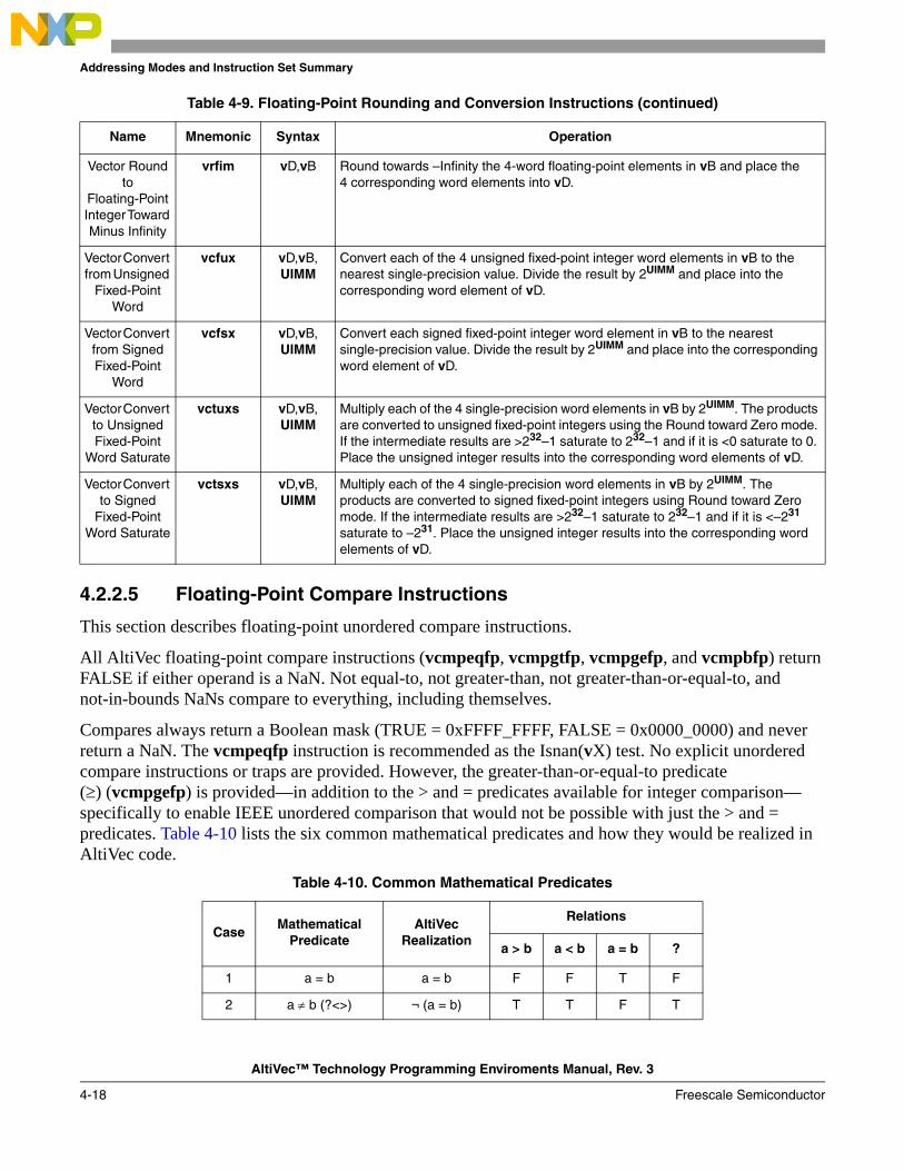
Addressing Modes and Instruction Set Summary
AltiVec™ Technology Programming Enviroments Manual, Rev. 3
4-18 Freescale Semiconductor
4.2.2.5 Floating-Point Compare Instructions
This section describes floating-point unordered compare instructions.
All AltiVec floating-point compare instructions (vcmpeqfp, vcmpgtfp, vcmpgefp, and vcmpbfp) return FALSE if either operand is a NaN. Not equal-to, not greater-than, not greater-than-or-equal-to, and not-in-bounds NaNs compare to everything, including themselves.
Compares always return a Boolean mask (TRUE = 0xFFFF_FFFF, FALSE = 0x0000_0000) and never return a NaN. The vcmpeqfp instruction is recommended as the Isnan(vX) test. No explicit unordered compare instructions or traps are provided. However, the greater-than-or-equal-to predicate (≥) (vcmpgefp) is provided—in addition to the > and = predicates available for integer comparison— specifically to enable IEEE unordered comparison that would not be possible with just the > and = predicates. Table 4-10 lists the six common mathematical predicates and how they would be realized in AltiVec code.
Vector Round to
Floating-Point Integer Toward Minus Infinity
vrfim vD,vB Round towards –Infinity the 4-word floating-point elements in vB and place the 4 corresponding word elements into vD.
Vector Convert from Unsigned
Fixed-Point Word
vcfux vD,vB, UIMM
Convert each of the 4 unsigned fixed-point integer word elements in vB to the nearest single-precision value. Divide the result by 2UIMM and place into the corresponding word element of vD.
Vector Convert from Signed Fixed-Point
Word
vcfsx vD,vB, UIMM
Convert each signed fixed-point integer word element in vB to the nearest single-precision value. Divide the result by 2UIMM and place into the corresponding word element of vD.
Vector Convert to Unsigned Fixed-Point
Word Saturate
vctuxs vD,vB, UIMM
Multiply each of the 4 single-precision word elements in vB by 2UIMM. The products are converted to unsigned fixed-point integers using the Round toward Zero mode. If the intermediate results are >232–1 saturate to 232–1 and if it is <0 saturate to 0. Place the unsigned integer results into the corresponding word elements of vD.
Vector Convert to Signed
Fixed-Point Word Saturate
vctsxs vD,vB, UIMM
Multiply each of the 4 single-precision word elements in vB by 2UIMM. The products are converted to signed fixed-point integers using Round toward Zero mode. If the intermediate results are >232–1 saturate to 232–1 and if it is <–231 saturate to –231. Place the unsigned integer results into the corresponding word elements of vD.
Table 4-10. Common Mathematical Predicates
CaseMathematical
PredicateAltiVec
Realization
Relations
a > b a < b a = b ?
1 a = b a = b F F T F
2 a ≠ b (?<>) ¬ (a = b) T T F T
Table 4-9. Floating-Point Rounding and Conversion Instructions (continued)
Name Mnemonic Syntax Operation

Addressing Modes and Instruction Set Summary
AltiVec™ Technology Programming Enviroments Manual, Rev. 3
Freescale Semiconductor 4-19
Table 4-11 shows the remaining eight useful predicates and how they might be realized in AltiVec code.
The vector floating-point compare instructions compare the elements in two vector registers word-by-word, interpreting the elements as single-precision numbers. With the exception of the Vector Compare Bounds Floating-Point (vcmpbfp) instruction they set the target vector register, and CR[6] if Rc = 1, in the same manner as do the vector integer compare instructions.
The Vector Compare Bounds Floating-Point (vcmpbfp) instruction sets the target vector register, and CR[6] if Rc = 1, to indicate whether the elements in vA are within the bounds specified by the corresponding element in vB, as explained in the instruction description. A single-precision value x is said to be within the bounds specified by a single-precision value y if (–y ≤ x ≤ y).
3 a > b a > b T F F F
4 a < b b > a F T F F
5 a ≥ b ¬ (b > a) T F T *T
6 a ≤ b ¬ (a > b) F T T *T
5a a ≥ b a ≥ b T F T F
6a a ≤ b b ≥ a F T T F
Note: Cases 5 and 6 implemented with greater-than (vcmpgtfp and vnor) would not yield the correct IEEE result when the relation is unordered.
Table 4-11. Other Useful Predicates
Case PredicateAltiVec
Realization
Relations
a > b a < b a = b ?
7 a ? b ¬ ((a = b) ∨ (b > a) ∨ (a > b)) F F F T
8 a <> b (a ≥ b) ⊕ (b ≥ a) T T F F
9 a <=> b (a ≥ b) ∨ (b ≥ a) T T T F
10 a ?> b ¬ (b ≥ a) T F F T
11 a ?>= b ¬ (b > a) T F T T
12 a ?< b ¬ (a ≥ b) F T F T
13 a ?<= b ¬ (a > b) F T T T
14 a ?= b ¬ ((a > b) ∨ (b > a)) F F T T
Table 4-10. Common Mathematical Predicates (continued)
CaseMathematical
PredicateAltiVec
Realization
Relations
a > b a < b a = b ?

Addressing Modes and Instruction Set Summary
AltiVec™ Technology Programming Enviroments Manual, Rev. 3
4-20 Freescale Semiconductor
The floating-point compare instructions are summarized in Table 4-12.Table 4-12. Floating-Point Compare Instructions
Name Mnemonic Syntax Operation
Vector Compare
Greater Than Floating-Point
[Record]
vcmpgtfp[.] vD,vA,vB
Compare each of the 4 single-precision word elements in vA to the corresponding 4 single-precision word elements in vB.For each element, if vA > vB, then set the corresponding element in vD to all 1s, otherwise clear the element in vD to all 0s.If the record bit is set (Rc = 1) in the vector compare instruction, then vD ==1, (all elements true) then CR6[0] is setvD == 0, (all elements false) then CR6[2] is set
Vector CompareEqual to
Floating-Point [Record]
vcmpeqfp[.] vD,vA,vB
Compare each of the 4 single-precision word elements in vA to the corresponding 4 single-precision word elements in vB.For each element, if vA = vB, then set the corresponding element in vD to all 1s, otherwise clear the element in vD to all 0s.If the record bit is set (Rc = 1) in the vector compare instruction then vD ==1, (all elements true) then CR6[0] is setvD == 0, (all elements false) then CR6[2] is set
Vector Compare
Greater Than or Equal to
Floating-Point [Record]
vcmpgefp[.] vD,vA,vB
Compare each of the 4 single-precision word elements in vA to the corresponding 4 single-precision word elements in vB.For each element, if vA >= vB, then set the corresponding element in vD to all 1s, otherwise clear the element in vD to all 0s.If the record bit is set (Rc = 1) in the vector compare instruction then vD ==1, (all elements true) then CR6[0] is setvD == 0, (all elements false) then CR6[2] is set
Vector CompareBounds
Floating-Point [Record]
vcmpbfp[.] vD,vA,vB
Compare each of the 4 single-precision word elements in vA to the corresponding single-precision word elements in vB. A 2-bit value is formed that indicates whether the element in vA is within the bounds specified by the element in vB, as follows.Bit 0 of the 2-bit value is cleared if the element in vA is <= to the element in vB, and is set otherwise.Bit 1 of the 2-bit value is cleared if the element in vA is >= to the negation of the element in vB, and is set otherwise.The 2-bit value is placed into the high-order 2 bits of the corresponding word element of vD and the remaining bits of the element are cleared to 0.If Rc = 1, CR6[2] is set when all 2 elements in vA are within the bounds specified by the corresponding element in vB.

Addressing Modes and Instruction Set Summary
AltiVec™ Technology Programming Enviroments Manual, Rev. 3
Freescale Semiconductor 4-21
4.2.2.6 Floating-Point Estimate Instructions
The floating-point estimate instructions are summarized in Table 4-13.
4.2.3 Load and Store Instructions
Only very basic load and store operations are provided in AltiVec ISA. This keeps the circuitry in the memory path fast so the latency of memory operations will be low. Instead, a powerful set of field manipulation instructions are provided to manipulate data into the desired alignment and arrangement after the data has been brought into the vector registers.
Load vector indexed (lvx, lvxl) and store vector indexed (stvx, stvxl) instructions transfer an aligned quad-word vector between memory and vector registers. Load vector element indexed (lvebx, lvehx, lvewx) and store vector element indexed instructions (stvebx, stvehx, stvewx) transfer byte, half-word, and word scalar elements between memory and vector registers.
All vector loads and vector stores use the index (rA|0 + rB) addressing mode to specify the target memory address. AltiVec ISA does not provide any update forms. An lvebx, lvehx, or lvewx instruction transfers a scalar data element from memory into the destination vector register, leaving other elements in the vector with boundedly-undefined values. A stvebx, stvehx, or stvewx instruction transfers a scalar data element from the source vector register to memory leaving other elements in the quad word unchanged. No data alignment occurs, that is, all scalar data elements are transferred directly on their natural memory byte-lanes to or from the corresponding element in the vector register. Quad-word memory accesses made by lvx, lvxl, stvx, and stvxl instructions are not guaranteed to be atomic. Direct-store segments (T = 1) are not supported by AltiVec ISA. Any vector load or store that attempts to access a direct-store segment will cause a data storage interrupt.
4.2.3.1 Alignment
All memory references must be size aligned. If a vector load or store address is not properly size-aligned, the suitable number of least significant bits are ignored, and a size-aligned transfer occurs instead. Data
Table 4-13. Floating-Point Estimate Instructions
Name Mnemonic Syntax Operation
Vector Reciprocal Estimate
Floating-Point
vrefp vD,vB Place estimates of the reciprocal of each of the 4-word floating-point source elements in vB in the corresponding 4-word elements in vD.
Vector Reciprocal Square Root
Estimate Floating-Point
vrsqrtefp vD,vB Place estimates of the reciprocal square-root of each of the 4-word source elements in vB in the corresponding 4-word elements in vD.
Vector Log2 Estimate
Floating-Point
vlogefp vD,vB Place estimates of the base 2 logarithm of each of the 4-word source elements in vB in the corresponding 4-word elements in vD.
Vector 2 Raised to the Exponent
Estimate Floating-Point
vexptefp vD,vB Place estimates of 2 raised to the power of each of the 4-word source elements in vB in the corresponding 4-word elements in vD.

Addressing Modes and Instruction Set Summary
AltiVec™ Technology Programming Enviroments Manual, Rev. 3
4-22 Freescale Semiconductor
alignment must be performed by software after being brought into the registers. No assistance is provided for aligning individual scalar elements that are not aligned on their natural size boundary. However, assistance is provided for justifying non-size-aligned vectors. This is provided through the Load Vector for Shift Left (lvsl) and Load Vector for Shift Right (lvsr) instructions that compute the proper Vector Permute (vperm) control vector from the misaligned memory address. For details on how to use these instructions to align data see Section 3.1.6, “Quad-Word Data Alignment.”
The lvx, lvxl, stvx, and stvxl instructions can be used to move data, not just multimedia data, in PowerPC environments. Therefore, because vector loads and stores are size-aligned, care should be taken to align data on even quad-word boundaries for maximum performance.
4.2.3.2 Load and Store Address Generation
Vector load and store operations generate effective addresses using register indirect with index mode.
All AltiVec load and store instructions use register indirect with index addressing mode that cause the contents of two GPRs (specified as operands rA and rB) to be added in the generation of the effective address (EA). A 0 in place of the rA operand causes a 0 to be added to the value specified by rB. The option to specify rA or 0 is shown in the instruction descriptions as (rA|0). If the address becomes misaligned, for a half-word, word, or quad word when combining addresses (rA|0 + rB), the effective address is ANDed with the appropriate 0 values to boundary align the address and is summarized in Table 4-14.
Table 4-14. Effective Address Alignment
Operand Effective Address Bit Setting
Indexed half-word EA[63] 0b0
Indexed word EA[62–63] 0b00
Indexed quad word EA[60–63] 0b0000

Addressing Modes and Instruction Set Summary
AltiVec™ Technology Programming Enviroments Manual, Rev. 3
Freescale Semiconductor 4-23
Figure 4-1 shows how an effective address is generated when using register indirect with index addressing.
Figure 4-1. Register Indirect with Index Addressing for Loads/Stores
4.2.3.3 Vector Load Instructions
For vector load instructions, the byte, half-word, or word addressed by the EA (effective address) is loaded into rD.
The default byte and bit ordering is big-endian as in the PowerPC architecture; see Section 3.1.2, “AltiVec Byte Ordering,” for information about little-endian byte ordering.
No
0 63
GPR (rA)
0
+
0 63
VR (vD)Memory Interface
StoreLoad
Yes
0 63
GPR (rB)
Instruction Encoding:
rA=0?
0 63
Effective Address
0 5 6 1011 1516 20 21 30 31
Opcode vD/vS rA rB Subopcode 0Reserved
Boundary Align EA

Addressing Modes and Instruction Set Summary
AltiVec™ Technology Programming Enviroments Manual, Rev. 3
4-24 Freescale Semiconductor
Table 4-15 summarizes the vector load instructions.
The lvsl and lvsr instructions can be used to create the permute control vector to be used by a subsequent vperm instruction. Let X and Y be the contents of vA and vB specified by vperm. The control vector created by lvsl causes the vperm to select the high-order 16 bytes of the result of shifting the 32-byte value X || Y left by sh bytes (sh = the value in EA[60–63]). The control vector created by lvsr causes the vperm to select the low-order 16 bytes of the result of shifting X || Y right by sh bytes.
These instructions can also be used to rotate or shift the contents of a vector register left lvsl or right lvsr by sh bytes. The sh values for the lvsl instruction are shown in Table 4-17, and those for the lvsr instruction are shown in Table 4-18. For rotating, the vector register to be rotated should be specified as both the vA and the vB register for vperm. For shifting left, the vB register for vperm should be a register containing all zeros and vA should contain the value to be shifted, and vice versa for shifting right. For further examples on how to align the data see Section 3.1.6, “Quad-Word Data Alignment.” The default byte and bit ordering is big-endian as in the PowerPC architecture; see Section 3.1.2.2, “Little-Endian Byte Ordering,” for information about little-endian byte ordering.
Table 4-15. Integer Load Instructions
Name Mnemonic Syntax Operation
Load Vector Element Integer Indexed [b,h,w]
lvebxlvehxlvewx
vD,rA,rB
The EA is the sum (rA|0) + (rB). Load the byte, half-word, or word in memory addressed by the EA into the low-order bits of vD. The remaining bits in vD are set to boundedly-undefined values.Because memory must stay aligned, the EA is set to default to alignment:For b, byte, integer length = 8 bits = 1 byte, For h, half-word, integer length = 16 bits = 2 bytes, EA[62–63] is set to 0b0For w, word, integer length = 32 bits = 4 bytes, EA[61–63] is set to 0b00
Load Vector Indexed
lvx vD,rA,rB
The EA is the sum (rA|0) + (rB). Load the double word in memory addressed by the EA into vD.Because memory needs to stay aligned, the EA is set to default to alignment:For a quad word, integer length = 128 bits = 16 bytes, EA[60–63] is set to 0b0000LRU = 0If the processor is in little-endian mode, load the double word in memory addressed by EA into vD[64–127] and load the double word in memory addressed by EA + 8 into vD[0–63].
Load Vector Indexed LRU
lvxl vD,rA,rB
The EA is the sum (rA|0) + (rB). Load the double word in memory addressed by the EA into vD.For the double word, integer length = 64 bits = 8 bytes, the EA[60–63] is set to 0b0000.LRU = 1, least recently used, hints that the quad word in the memory addressed by EA will probably not be needed again by the program in the near future.If the processor is in little-endian mode, load the double word in memory addressed by EA into vD[64–127] and load the double word in memory addressed by EA + 8 into vD[0–63].

Addressing Modes and Instruction Set Summary
AltiVec™ Technology Programming Enviroments Manual, Rev. 3
Freescale Semiconductor 4-25
Table 4-16 summarizes the vector alignment instructions.Table 4-16. Vector Load Instructions Supporting Alignment
Name Mnemonic Syntax Operation
Load Vector for Shift Left
lvsl vD,rA,rB
The EA is the sum (rA|0) + (rB). The EA[60–63] = sh, then based on Table 4-17, place the value in vD
Load Vector for Shift Right
lvsr vD,rA,rB
The EA is the sum (rA|0) + (rB). The EA[60–63] = sh, then based on Table 4-18, place the value in vD
Table 4-17. Shift Values for lvsl Instruction
Shift (sh) vD[0–127]
0x0 0x000102030405060708090A0B0C0D0E0F
0x1 0x0102030405060708090A0B0C0D0E0F10
0x2 0x02030405060708090A0B0C0D0E0F1011
0x3 0x0D0E0F101112131415161718191A1B1C
0x4 0x0405060708090A0B0C0D0E0F10111213
0x5 0x05060708090A0B0C0D0E0F1011121314
0x6 0x060708090A0B0C0D0E0F101112131415
0x7 0x0708090A0B0C0D0E0F10111213141516
0x8 0x08090A0B0C0D0E0F1011121314151617
0x9 0x090A0B0C0D0E0F101112131415161718
0xA 0x0A0B0C0D0E0F10111213141516171819
0xB 0x0B0C0D0E0F101112131415161718191A
0xC 0x0C0D0E0F101112131415161718191A1B
0xD 0x0D0E0F101112131415161718191A1B1C
0xE 0x0E0F101112131415161718191A1B1C1D
0xF 0x0F101112131415161718191A1B1C1D1E
Table 4-18. Shift Values for lvsr Instruction
Shift (sh) vD[0–127]
0x0 0x101112131415161718191A1B1C1D1E1F
0x1 0x0F101112131415161718191A1B1C1D1E
0x2 0x0E0F101112131415161718191A1B1C1D
0x3 0x0D0E0F101112131415161718191A1B1C
0x4 0x0C0D0E0F101112131415161718191A1B
0x5 0x0B0C0D0E0F101112131415161718191A
0x6 0x0A0B0C0D0E0F10111213141516171819
0x7 0x090A0B0C0D0E0F101112131415161718
0x8 0x08090A0B0C0D0E0F1011121314151617
0x9 0x0708090A0B0C0D0E0F10111213141516

Addressing Modes and Instruction Set Summary
AltiVec™ Technology Programming Enviroments Manual, Rev. 3
4-26 Freescale Semiconductor
4.2.3.4 Vector Store Instructions
For vector store instructions, the contents of vector register used as a source (vS) are stored into the byte, half-word, word, or quad word in memory addressed by the effective address (EA). Table 4-19 provides a summary of the vector store instructions.
4.2.4 Control Flow
AltiVec instructions can be freely intermixed with existing PowerPC instructions to form a complete program. AltiVec instructions do provide a vector compare and select mechanism to implement conditional execution as a mechanism to control data flow in AltiVec programs. Also, the AltiVec vector
0xA 0x060708090A0B0C0D0E0F101112131415
0xB 0x05060708090A0B0C0D0E0F1011121314
0xC 0x0405060708090A0B0C0D0E0F10111213
0xD 0x030405060708090A0B0C0D0E0F101112
0xE 0x02030405060708090A0B0C0D0E0F1011
0xF 0x0102030405060708090A0B0C0D0E0F10
Table 4-19. Integer Store Instructions
Name Mnemonic Syntax Operation
Store Vector Element Integer Indexed[b,h,w]
stvebxstvehxstvewx
vS,rA,rB
The EA is the sum (rA|0) + (rB). Store the contents of the low-order bits of vS into the integer in memory addressed by the EA.Because memory needs to stay aligned, the EA is set to default to alignment:For b, byte, integer length = 8 bits = 1 byte For h, half-word, integer length = 16 bits = 2 bytes, EA[62–63] is set to 0b0For w, word, integer length = 32 bits = 4 bytes, EA[61–63] is set to 0b00
Store Vector Indexed
stvx vS,rA,rB
The EA is the sum (rA|0) + (rB). Store the contents of vS into the quad word in memory addressed by the EA.For q, quad word, integer length = 128 bits = 16 bytes, the EA[60–63] is set to 0b0000LRU = 0If the processor is in little-endian mode, store the contents of vS[64–127] into the double word in memory addressed by EA, and store the contents of vS[0–63] into the double word in memory addressed by EA + 8.
Store Vector Indexed LRU
stvxl vD,rA,rB
The EA is the sum (rA|0) + (rB). Store the contents of vS into the quad word in memory addressed by the EA.For d, double word, integer length = 64 bits = 8 bytes, the EA[60–63] is set to 0b0000LRU = 1, least recently used, hints that the quad word in the memory addressed by EA will probably not be needed again by the program in the near future.If the processor is in little-endian mode, store the contents of vS[64–127] into the double word in memory addressed by EA, and store the contents of vS[0–63] into the double word in memory addressed by EA + 8.
Table 4-18. Shift Values for lvsr Instruction (continued)
Shift (sh) vD[0–127]

Addressing Modes and Instruction Set Summary
AltiVec™ Technology Programming Enviroments Manual, Rev. 3
Freescale Semiconductor 4-27
compare instructions can update the condition register, thus, providing the communication from AltiVec execution units to PowerPC branch instructions necessary to modify program flow based on vector data.
4.2.5 Vector Permutation and Formatting Instructions
Vector pack, unpack, merge, splat, permute, and select can be used to accelerate various vector math and vector formatting. Details of the various instructions follow.
4.2.5.1 Vector Pack Instructions
Half-word vector pack instructions (vpkuhum, vpkuhus, vpkshus, vpkshss) truncate the 16 half-words from 2 concatenated source operands producing a single result of 16 bytes (quad word) using either modulo(28), 8-bit signed-saturation, or 8-bit unsigned-saturation to perform the truncation. Similarly, word vector pack instructions (vpkuwum, vpkuwus, vpkswus, and vpksws) truncate the 8 words from 2 concatenated source operands producing a single result of 8 half-words using modulo(2^16), 16-bit signed-saturation, or 16-bit unsigned-saturation to perform the truncation.
One special form of Vector Pack Pixel (vpkpx) instruction packs eight 32-bit (8/8/8/8) pixels from two concatenated source operands into a single result of eight 16-bit 1/5/5/5 αRGB pixels. The least significant bit of the first 8-bit element becomes the 1-bit α field, and each of the three 8-bit R, G, and B fields are reduced to 5 bits by ignoring the 3 lsbs.
Table 4-20 describes the vector pack instructions.Table 4-20. Vector Pack Instructions
Name Mnemonic Syntax Operation
Vector Pack Unsigned
Integer [h,w] Unsigned Modulo
vpkuhumvpkuwum
vD,vA,vB
Concatenate the low-order unsigned integers of vA and the low-order unsigned integers of vB and place into vD using unsigned modulo arithmetic. vA is placed in the lower order double word of vD and vB is placed into the higher order double word of vD. For h, half-word, integer length = 16 bits = 2 bytes, 8 unsigned integers, in other words, the 8 low-order bytes of the half-words from vA and vB.For w, word, integer length = 32 bits = 4 bytes, 4 unsigned integers, in other words, the 4 low-order half-words of the words from vA and vB.
Vector Pack Unsigned
Integer [h,w] Unsigned Saturate
vpkuhusvpkuwus
vD,vA,vB
Concatenate the low-order unsigned integers of vA and the low-order unsigned integers of vB and place into vD using unsigned saturate clamping mode. vA is placed in the lower order double word of vD and vB is placed into the higher order double word of vD. For h, half-word, integer length = 16 bits = 2 bytes, 8 unsigned integers, in other words, the 8 low-order bytes of the half-words from vA and vB.For w, word, integer length = 32 bits = 4 bytes, 4 unsigned integers, in other words, the 4 low-order words of the half-words from vA and vB.

Addressing Modes and Instruction Set Summary
AltiVec™ Technology Programming Enviroments Manual, Rev. 3
4-28 Freescale Semiconductor
4.2.5.2 Vector Unpack Instructions
Byte vector unpack instructions unpack the 8 low bytes (or 8 high bytes) of one source operand into 8 half-words using sign extension to fill the MSBs. Half-word vector unpack instructions, unpack the 4 low half-words (or 4 high half-words) of one source operand into 4 words using sign extension to fill the MSBs.
A special purpose form of vector unpack is provided, the Vector Unpack Low Pixel (vupklpx) and the Vector Unpack High Pixel (vupkhpx) instructions for 1/5/5/5 αRGB pixels. The 1/5/5/5 pixel vector unpack, unpacks the four low 1/5/5/5 pixels (or four 1/5/5/5 high pixels) into four 32-bit (8/8/8/8) pixels. The 1-bit α element in each pixel is sign extended to 8 bits, and the 5-bit R, G, and B elements are each zero extended to 8 bits.
Vector Pack Signed Integer
[h,w] Unsigned Saturate
vpkshusvpkswus
vD,vA,vB
Concatenate the low-order signed integers of vA and the low-order signed integers of vB and place into vD using unsigned saturate clamping mode. vA is placed in the lower order double word of vD and vB is placed into the higher order double word of vD. For h, half-word, integer length = 16 bits = 2 bytes, 8 signed integers, in other words, the 8 low-order bytes of the half-word from vA and vB.For w, word, integer length = 32 bits = 4 bytes, 4 signed integers, in other words, the 4 low-order half-words of the words from vA and vB.
Vector Pack Signed Integer [h,w] Signed
Saturate
vpkshssvpkswss
vD,vA,vB
Concatenate the low-order signed integers of vA and the low-order signed integers of vB are concatenated and place into vD using signed saturate clamping mode. vA is placed in the lower order double word of vD and vB is placed into the higher order double word of vD. For h, half-word, integer length = 16 bits = 2 bytes, 8 signed integers, in other words, the 8 low-order bytes of the half-word from vA and vB.For w, word, integer length = 32 bits = 4 bytes, 4 signed integers, in other words, the 4 low-order half-words of the words from vA and vB.
Vector Pack Pixel
vpkpx vD,vA,vB
Each word element in vA and vB is packed to 16 bits and the half-word is placed into vD. Each word from vA and vB is packed to 16 bits in the following order:[bit 7 of the first byte (bit 7 of the word)][bits 0–4 of the second byte (bits 8–12 of the word)[bits 0–4 of the third byte (bits 16–20 of the word)][bits 0–4 of the fourth byte (bits 24–28 of the word)]vA half-words are placed in the lower order double word of vD and vB half-words are placed into the higher order double word of vD. For h, half-word, integer length = 16 bits = 2 bytes, 8 signed integers, in other words, the 8 low-order bytes of the half-word from vA and vB.For w, word, integer length = 32 bits = 4 bytes, 4 signed integers, in other words, the 4 low-order half-words of the words from vA and vB.
Table 4-20. Vector Pack Instructions (continued)
Name Mnemonic Syntax Operation

Addressing Modes and Instruction Set Summary
AltiVec™ Technology Programming Enviroments Manual, Rev. 3
Freescale Semiconductor 4-29
Table 4-21 describes the unpack instructions.
4.2.5.3 Vector Merge Instructions
Byte vector merge instructions interleave the 8 low bytes (or 8 high bytes) from two source operands producing a result of 16 bytes. Similarly, half-word vector merge instructions interleave the 4 low half-words (or 4 high half-words) of two source operands producing a result of 8 half-words, and word vector merge instructions interleave the 2 low words (or t2wo high words) from two source operands producing a result of 4 words. The vector merge instruction has many uses, notable among them is a way to efficiently transpose SIMD vectors. Table 4-22 describes the merge instructions.
Table 4-21. Vector Unpack Instructions
Name Mnemonic Syntax Operation
Vector Unpack High SignedInteger [b,h]
vupkhsbvupkhsh
vD,vB Each signed integer element in the high order double word of vB is sign extended to fill the MSBs in a signed integer and then is placed into vD. For b, byte, integer length = 8 bits = 1 byte, 8 signed bytes from the high order double word of vB are unpacked and sign extended to 8 half-words into vD.For h, half-word, integer length = 16 bits = 2 bytes, 8 signed half-words from the high order double word of vB are unpacked and sign extended to 4 words into vD
Vector Unpack High Pixel
vupkhpx vD,vB Each half-word element in the high order double word of vB is unpacked to produce a 32-bit word that is then placed in the same order into vD. A half-word element is unpacked to 32 bits by concatenating, in order, the results of the following operations.
sign-extend bit 0 of the half-word to 8 bitszero-extend bits 1–5 of the half-word to 8 bitszero-extend bits 6–10 of the half-word to 8 bitszero-extend bits 11–15 of the half-word to 8 bits
Vector Unpack Low SignedInteger [b,h]
vupklsbvupklsh
vD,vB Each signed integer element in the low-order double word of vB is sign extended to fill the MSBs in a signed integer and then is placed into vD. For b, byte, integer length = 8 bits = 1 byte, 8 signed bytes from the low-order double word of vB are unpacked and sign extended to 8 half-words into vD.For h, half-word, integer length = 16 bits = 2 bytes, 8 signed half-words from the low-order double word of vB are unpacked and sign extended into 4 words in vD.
Vector Unpack Low Pixel
vupklpx vD,vB Each half-word element in the low-order double word of vB is unpacked to produce a 32-bit word that is then placed in the same order into vD. A half-word element is unpacked to 32 bits by concatenating, in order, the results of the following operations.
sign-extend bit 0 of the half-word to 8 bitszero-extend bits 1–5 of the half-word to 8 bitszero-extend bits 6–10 of the half-word to 8 bitszero-extend bits 11–15 of the half-word to 8 bits

Addressing Modes and Instruction Set Summary
AltiVec™ Technology Programming Enviroments Manual, Rev. 3
4-30 Freescale Semiconductor
4.2.5.4 Vector Splat Instructions
When a program needs to perform arithmetic vector, the vector splat instructions can be used in preparation for performing arithmetic for which one source vector is to consist of elements that all have the same value (for example, multiplying all elements of a Vector Register by a constant). Vector splat instructions can be used to move data where it is required. For example, to multiply all elements of a vector register by a constant, the vector splat instructions can be used to splat the scalar into the vector register. Likewise, when storing a scalar into an arbitrary memory location, it must be splatted into a vector register, and that register must be specified as the source of the store. This will guarantee that the data appears in all possible positions of that scalar size for the store. Table 4-23 describes the vector splat instructions.
Table 4-22. Vector Merge Instructions
Name Mnemonic Syntax Operation
Vector Merge High Integer
[b,h,w]
vmrghbvmrghhvmrghw
vD,vA,vB
Each integer element in the high order double word of vA is placed into the low-order integer element in vD. Each integer element in the high order double word of vB is placed into the high order integer element in vD.For b, byte, integer length = 8 bits = 1 byte, 8 bytes from the high order double word of vA are placed into the low-order byte of each half-word in vD and 8 bytes from the high order double word of vB are placed into the high order byte of each half-word in vD.For h, half-word, integer length = 16 bits = 2 bytes, 4 half-words from the high order double word of vA are placed into the low-order half-word of each word in vD and four half-words from the high order double word of vB are placed into the high order half-word of each word in vD.For w, word, integer length = 32 bits = 4 bytes, 2 words from the high order double word of vA are placed into the low-order word of each double word in vD and 2 words from the high order double word of vB are placed into the high order word of each double word in vD.
Vector Merge Low Integer
[b,h,w]
vmrglbvmrglhvmrglw
vD,vA,vB
Each integer element in the low-order double word of vA is placed into the low-order integer element in vD. Each integer element in the low-order double word of vB is placed into the high order integer element in vD.For b, byte, integer length = 8 bits = 1 byte, 8 bytes from the low-order double word of vA are placed into the low-order byte of each half-word in vD and 8 bytes from the low-order double word of vB are placed into the high order byte of each half-word in vD.For h, half-word, integer length = 16 bits = 2 bytes, 4 half-words from the low-order double word of vA are placed into the low-order half-word of each word in vD and 4 half-words from the low-order double word of vB are placed into the high order half-word of each word in vD.For w, word, integer length = 32 bits = 4 bytes, 2 words from the low-order double word of vA are placed into the low-order word of each double word in vD and 2 words from the low-order double word of vB are placed into the high order word of each double word in vD.

Addressing Modes and Instruction Set Summary
AltiVec™ Technology Programming Enviroments Manual, Rev. 3
Freescale Semiconductor 4-31
4.2.5.5 Vector Permute Instruction
Permute instructions allow any byte in any two source vector registers to be directed to any byte in the destination vector. The fields in a third source operand specify from which field in the source operands the corresponding destination field will be taken. The Vector Permute (vperm) instruction is a very powerful one that provides many useful functions. For example, it provides a good way to perform table-lookups and data alignment operations. An example of how to use the command in aligning data is shown in Section 3.1.6, “Quad-Word Data Alignment.” Table 4-24 describes the vector permute instruction.
4.2.5.6 Vector Select Instruction
Data flow in the vector unit can be controlled without branching by using a vector compare and the vector select (vsel) instructions. In this use, the compare result vector is used directly as a mask operand to vector select instructions.The vsel instruction selects one field from one or the other of two source operands under control of its mask operand. Use of the TRUE/FALSE compare result vector with select in this manner produces a two instruction equivalent of conditional execution on a per-field basis. Table 4-25 describes the vsel instruction.
4.2.5.7 Vector Shift Instructions
The vector shift instructions shift the contents of a vector register or of a pair of vector registers left or right by a specified number of bytes (vslo, vsro, vsldoi) or bits (vsl, vsr). Depending on the instruction, this shift count is specified either by low-order bits of a vector register or by an immediate field in the instruction.
Table 4-23. Vector Splat Instructions
Name Mnemonic Syntax Operation
Vector Splat Integer [b,h,w]
vspltbvsplthvspltw
vD,vB,UIMM
Replicate the contents of element UIMM in vB and place into each element in vD.For b, byte, integer length = 8 bits = 1 byte, each element is a byte.For h, half-word, integer length = 16 bits = 2 bytes, each element is a half-word.For w, word, integer length = 32 bits = 4 bytes, two words each element is a word.
Vector Splat Immediate
Signed Integer [b,h,w]
vspltisbvspltishvspltisw
vD,SIMM
Sign-extend the value of the SIMM field to the length of the element and replicate that value and place into each element in vD.For b, byte, integer length = 8 bits = 1 byte, each element is a byte.For h, half-word, integer length = 16 bits = 2 bytes, each element is a half-word.For w, word, integer length = 32 bits = 4 bytes, 2 words each element is a word.
Table 4-24. Vector Permute Instruction
Name Mnemonic Syntax Operation
Vector Permute
vperm vD,vA,vB,vC
vC specifies which bytes from vA and vB are to be copied and placed into the byte elements in vD.
Table 4-25. Vector Select Instruction
Name Mnemonic Syntax Operation
Vector Select
vsel vD,vA,vB,vC
For each bit, compare the value in vC to the value 0b0 and if it equals 0b0, then load vD with vA’s corresponding bit value, otherwise compare the value in vC to the value 0b1 and if it equals 0b1, then load vD with vB’s corresponding bit value.
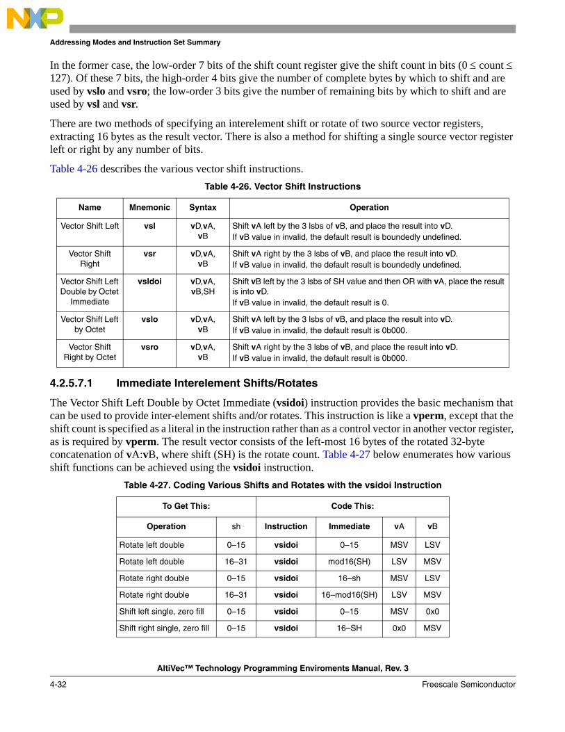
Addressing Modes and Instruction Set Summary
AltiVec™ Technology Programming Enviroments Manual, Rev. 3
4-32 Freescale Semiconductor
In the former case, the low-order 7 bits of the shift count register give the shift count in bits (0 ≤ count ≤ 127). Of these 7 bits, the high-order 4 bits give the number of complete bytes by which to shift and are used by vslo and vsro; the low-order 3 bits give the number of remaining bits by which to shift and are used by vsl and vsr.
There are two methods of specifying an interelement shift or rotate of two source vector registers, extracting 16 bytes as the result vector. There is also a method for shifting a single source vector register left or right by any number of bits.
Table 4-26 describes the various vector shift instructions.
4.2.5.7.1 Immediate Interelement Shifts/Rotates
The Vector Shift Left Double by Octet Immediate (vsidoi) instruction provides the basic mechanism that can be used to provide inter-element shifts and/or rotates. This instruction is like a vperm, except that the shift count is specified as a literal in the instruction rather than as a control vector in another vector register, as is required by vperm. The result vector consists of the left-most 16 bytes of the rotated 32-byte concatenation of vA:vB, where shift (SH) is the rotate count. Table 4-27 below enumerates how various shift functions can be achieved using the vsidoi instruction.
Table 4-26. Vector Shift Instructions
Name Mnemonic Syntax Operation
Vector Shift Left vsl vD,vA,vB
Shift vA left by the 3 lsbs of vB, and place the result into vD.If vB value in invalid, the default result is boundedly undefined.
Vector Shift Right
vsr vD,vA,vB
Shift vA right by the 3 lsbs of vB, and place the result into vD.If vB value in invalid, the default result is boundedly undefined.
Vector Shift Left Double by Octet
Immediate
vsldoi vD,vA,vB,SH
Shift vB left by the 3 lsbs of SH value and then OR with vA, place the result is into vD.If vB value in invalid, the default result is 0.
Vector Shift Left by Octet
vslo vD,vA,vB
Shift vA left by the 3 lsbs of vB, and place the result into vD.If vB value in invalid, the default result is 0b000.
Vector Shift Right by Octet
vsro vD,vA,vB
Shift vA right by the 3 lsbs of vB, and place the result into vD.If vB value in invalid, the default result is 0b000.
Table 4-27. Coding Various Shifts and Rotates with the vsidoi Instruction
To Get This: Code This:
Operation sh Instruction Immediate vA vB
Rotate left double 0–15 vsidoi 0–15 MSV LSV
Rotate left double 16–31 vsidoi mod16(SH) LSV MSV
Rotate right double 0–15 vsidoi 16–sh MSV LSV
Rotate right double 16–31 vsidoi 16–mod16(SH) LSV MSV
Shift left single, zero fill 0–15 vsidoi 0–15 MSV 0x0
Shift right single, zero fill 0–15 vsidoi 16–SH 0x0 MSV

Addressing Modes and Instruction Set Summary
AltiVec™ Technology Programming Enviroments Manual, Rev. 3
Freescale Semiconductor 4-33
4.2.5.7.2 Computed Interelement Shifts/Rotates
The Load Vector for Shift Left (lvsl) instruction and Load Vector for Shift Right (lvsr) instruction are supplied to assist in shifting and/or rotating vector registers by an amount determined at run time. The input specifications have the same form as the vector load and store instructions, that is, it uses register indirect with index addressing mode(rA|0 + rB). This is because one of their primary purposes is to compute the permute control vector necessary for post-load and pre-store shifting necessary for dealing with misaligned vectors.
This lvsl instruction can be used to align a big-endian misaligned vector after loading the (aligned) vectors that contain its pieces. The lvsl instruction can be used to misalign a vector register for use in a read-modify-write sequence that will store an misaligned little-endian vector.
The lvsr instruction can be used to align a little-endian misaligned vector after loading the (aligned) vectors that contain its pieces. The lvsl instruction can be used to misalign a vector register for use in a read-modify-write sequence that will store an misaligned big-endian vector.
For an example on how the lvsl instruction is used to align a vector in big-endian mode, see Section 3.1.6.1, “Accessing a Misaligned Quad Word in Big-Endian Mode.” For an example on how lvsr is used to align a vector in little-endian mode, see Section 3.1.6.2, “Accessing a Misaligned Quad Word in Little-Endian Mode.”
4.2.5.7.3 Variable Interelement Shifts
A vector register may be shifted left or right by a number of bits specified in a vector register. This operation is supported with four instructions, two for right shift and two for left shift.
The Vector Shift Left by Octet (vslo) and Vector Shift Right by Octet (vsro) instructions shift a vector register from 0 to 15 bytes as specified in bits 121–124 of another vector register. The Vector Shift Left (vsl) and Vector Shift Right (vsr) instructions shift a vector register from 0 to 7 bits as specified in another vector register (the shift count must be specified in the three lsbs of each byte in the vector and must be identical in all bytes or the result is boundedly undefined). In all of these instructions, zeros are shifted into vacated element and bit positions.
Used sequentially with the same shift-count vector register, these instructions will shift a vector register left or right from 0 to 127 bits as specified in bits 121–127 of the shift-count vector register. For example:
vslo VZ, VX, VY
vspltb VY, VY, 15
vsl VZ, VZ, VY
Rotate left single 0–15 vsidoi 0–15 MSV =VA
Rotate right single 0–15 vsidoi 16–SH MSV =VA
Table 4-27. Coding Various Shifts and Rotates with the vsidoi Instruction (continued)
To Get This: Code This:
Operation sh Instruction Immediate vA vB
Addressing Modes and Instruction Set Summary
AltiVec™ Technology Programming Enviroments Manual, Rev. 3
4-34 Freescale Semiconductor
will shift vX by the number of bits specified in vY and place the results in vZ.
With these instructions a full double-register shift can be performed in seven instructions. The following code will shift vW||vX left by the number of bits specified in vY placing the result in vZ:
vslo t1, VW, VY ; shift the most significant. register left
vspltb VY, VY, 15
vsl t1, t1, VY
vsububm VY, V0, VY ; adjust count for right shift (V0=0)
vsro t2, VX, VY ; right shift least sign. register
vsr t2, t2, VY
vor VZ, t1, t2 ; merge to get the final result
4.2.6 Processor Control Instructions—UISA
Processor control instructions are used to read from and write to the PowerPC condition register (CR), machine state register (MSR), and special-purpose registers (SPRs). See Chapter 4, “Addressing Mode and Instruction Set Summary,” in the Programming Environments Manual for 32-Bit Implementations of the PowerPC Architecture, for information about the instructions used for reading from and writing to the MSR and SPRs.
4.2.6.1 AltiVec Status and Control Register Instructions
Table 4-28 summarizes the instructions for reading from or writing to the Vector Status and Control Register (VSCR). For more information on VSCR see Section 2.3.2, “Vector Status and Control Register (VSCR).”
4.2.7 Recommended Simplified Mnemonics
To simplify assembly language programs, a set of simplified mnemonics is provided for some of the most frequently used operations (such as no-op, load immediate, load address, move register, and complement register). Assemblers could provide the simplified mnemonics listed below. Programs written to be portable across the various assemblers for PowerPC architecture should not assume the existence of mnemonics not described in this document.
Simplified mnemonics are provided for the Data Stream Touch (dst) and Data Stream Touch for Store
(dstst) instructions so that they can be coded with the transient indicator as part of the mnemonic rather than as a numeric operand. Similarly, simplified mnemonics are provided for the Data Stream Stop (dss) instruction so that it can be coded with the all streams indicator is part of the mnemonic. These are shown as examples with the instructions in Table 4-29.
Table 4-28. Move To/From Condition Register Instructions
Name Mnemonic Syntax Operation
Move to Vector Status and Control Register mtvscr CRM,rS Place the contents of vB into VSCR.
Move from Vector Status and Control Register mfvscr vB Place the contents of VSCR into vB.

Addressing Modes and Instruction Set Summary
AltiVec™ Technology Programming Enviroments Manual, Rev. 3
Freescale Semiconductor 4-35
4.3 AltiVec VEA InstructionsPowerPC virtual environment architecture (VEA) describes the semantics of thememory model that can be assumed by software processes, and includes descriptions of the cache model, cache-control instructions, address aliasing, and other related issues. Implementations that conform to the VEA also adhere to the UISA, but may not necessarily adhere to the OEA. For further details see Chapter 4, “Addressing Mode and Instruction Set Summary,” in the Programming Environments Manual for 32-Bit Implementations of the PowerPC Architecture.
This section describes the additional AltiVec instructions defined for the VEA.
4.3.1 Memory Control Instructions—VEA
Memory control instructions include the following types:• Cache management instructions (user-level and supervisor-level)• Segment register manipulation instructions• Segment lookaside buffer management instructions• Translation lookaside buffer (TLB) management instructions
This section describes the user-level cache management instructions defined by the VEA. See Chapter 4, “Addressing Mode and Instruction Set Summary,” in the Programming Environments Manual for 32-Bit Implementations of the PowerPC Architecture for more information about supervisor-level cache, segment register manipulation, and TLB management instructions.
4.3.2 User-Level Cache Instructions—VEA
The instructions summarized in this section provide user-level programs the ability to manage on-chip caches if they are implemented. See Chapter 5, “Cache Model and Memory Coherency,” in the Programming Environments Manual for 32-Bit Implementations of the PowerPC Architecture for more information about cache topics.
Bandwidth between the processor and memory is managed explicitly by the programmer through the use of cache management instructions. These instructions give software a way to communicate to the cache hardware how it should prefetch and prioritize writeback of data. The principal instruction for this purpose
Table 4-29. Simplified Mnemonics for Data Stream Touch (dst)
Operation Simplified Mnemonic Equivalent to
Data Stream Touch (Non-Transient) dst rA, rB, STRM dst rA, rB, STRM,0
Data Stream Touch Transient dstt rA, rB, STRM dst rA, rB, STRM,1
Data Stream Touch for Store (Non-Transient)
dstst rA, rB, STRM dstst rA, rB, STRM,0
Data Stream Touch for Transient dststt rA, rB, STRM dststt rA, rB, STRM,1
Data Stream Stop (One Stream) dss STRM dss STRM,0
Data Stream Stop All dssall dss 0,1

Addressing Modes and Instruction Set Summary
AltiVec™ Technology Programming Enviroments Manual, Rev. 3
4-36 Freescale Semiconductor
is a software directed cache prefetch instruction called Data Stream Touch (dst). Other related instructions are provided for complete control of the software directed cache prefetch mechanism.
Table 4-30 summarizes the directed prefetch cache instructions defined by the VEA. Note that these instructions are accessible to user-level programs. See Section 5.2.1, “Software-Directed Prefetch,” for further details on the prefetch cache instructions.
Table 4-30. User-Level Cache Instructions
Name Mnemonic Syntax Operation
Data Stream Touch
dst rA,rB,STRM,T
This instruction associates the data stream specified by the contents of rA and rB with the stream ID specified by STRM.The specified data stream is defined by the following:
EA: (rA), where rA ≠ 0unit size: (rB)[3–7] if (rB)[3–7] ≠ 0; otherwise 32count: (rB)[8–15] if (rB)[8–15 ] ≠ 0; otherwise 256stride: (rB)[16–31] if (rB)[16–31] ≠ 0; otherwise 32768
The T bit of the instruction indicates whether the data stream is likely to be stored into fairly frequently in the near future (T = 0) or to be transient (T = 1).If rA = 0, the instruction form is invalid.See Section 5.2.1.1, “Data Stream Touch (dst),” for further details on the dst instruction.
Data Stream Touch
dstt rA,rB,STRM,T
This instruction associates the data stream specified by the contents of registers rA and rB with the stream ID specified by STRM.This instruction is a hint that performance will probably be improved if the cache blocks containing the specified data stream are not fetched into the data cache, because the program will probably not load from the stream.That is, the data stream will be relatively transient in nature. That is, it will have poor locality and is likely to be referenced a very few times or over a very short period of time. The memory subsystem can use this persistent/transient knowledge to manage the data as is most appropriate for the specific design of the cache/memory hierarchy of the processor on which the program is executing. An implementation is free to ignore dstt, in that case, it should simply be executed as a dst. However, software should always attempt to use the correct form of dst or dstt regardless of whether the intended processor implements dstt. In this way the program will automatically benefit when run on processors that support dstt.The specified data stream is defined by the following:
EA: (rA), where rA ≠ 0unit size: (rB)[3–7] if (rB)[3–7] ≠0; otherwise 32count: (rB)[8–15] if (rB)[8–15] ≠ 0; otherwise 256stride: (rB)[16–31] if (rB)[16–31] ≠ 0; otherwise 32768
The T bit of the instruction indicates whether the data stream is likely to be accessed into fairly frequently in the near future (T = 0) or to be transient (T = 1).If rA = 0, the instruction form is invalid.See Section 5.2.1.2, “Transient Streams,” for further details on the dstt instruction.

Addressing Modes and Instruction Set Summary
AltiVec™ Technology Programming Enviroments Manual, Rev. 3
Freescale Semiconductor 4-37
Data Stream Touch for Store (Non-Transient)
dstst rA,rB,STRM,T
This instruction associates the data stream specified by the contents of registers rA and rB with the stream ID specified by STRM.This instruction is a hint that performance will probably be improved if the cache blocks containing the specified data stream are fetched into the data cache, because the program will probably soon access into the stream, and that prefetching from any data stream that was previously associated with the specified stream ID is no longer needed. The hint is ignored for blocks that are caching inhibited.The specified data stream is defined by the following:
EA: (rA), where rA ≠ 0unit size: (rB)[3–7] if (rB)[3-7] ≠ 0; otherwise 32count: (rB)[8–15] if (rB)[8–15] ≠ 0; otherwise 256stride: (rB)[16–31] if (rB)[16–31] ≠ 0; otherwise 32768
The T bit of the instruction indicates whether the data stream is likely to be stored into fairly frequently in the near future (T = 0) or to be transient (T = 1).If rA = 0, the instruction form is invalid.See Section 5.2.1.3, “Storing to Streams (dstst),” for further details on the dstst instruction.
Data Stream Touch for Store
dststt rA,rB,STRM,T
This instruction associates the data stream specified by the contents of rA and rB with the stream ID specified by STRM.This instruction is a hint that performance will probably not be improved if the cache blocks containing the specified data stream are fetched into the data cache, because the program will probably not access the stream. That is, the data stream will be relatively transient in nature. That is, it will have poor locality and is likely to be referenced a very few times or over a very short period of time. The memory subsystem can use this persistent/transient knowledge to manage the data as is most appropriate for the specific design of the cache/memory hierarchy of the processor on which the program is executing.The specified data stream is defined by the following:
EA: (rA), where rA ≠ 0unit size: (rB)[3–7] if (rB)[3-7] ≠ 0; otherwise 32count: (rB)[8–15] if (rB)[8–15] ≠ 0; otherwise 256stride: (rB)[16–31] if (rB)[16–31] ≠ 0; otherwise 32768
The T bit of the instruction indicates whether the data stream is likely to be stored into fairly frequently in the near future (T = 0) or to be transient (T = 1).If rA = 0, the instruction form is invalid.See Section 5.2.1.3, “Storing to Streams (dstst),” for further details on the dststt instruction.
Table 4-30. User-Level Cache Instructions (continued)
Name Mnemonic Syntax Operation

Addressing Modes and Instruction Set Summary
AltiVec™ Technology Programming Enviroments Manual, Rev. 3
4-38 Freescale Semiconductor
Data Stream Stop
dss STRM,A If A = 0 and a data stream associated with the stream ID specified by STRM exists, this instruction terminates prefetching of that data stream.If A = 1, this instruction terminates prefetching of all existing data streams. (The STRM field is ignored.)In addition, executing a dss instruction ensures that all memory accesses associated with data stream prefetching caused by preceding dst and dstst instructions that specified the same stream ID as that specified by the dss instruction (A = 0), or by all preceding dst and dstst instructions (A = 1), will be in group G1 with respect to the memory barrier created by a subsequent sync instruction.dss serves as both a basic and an extended mnemonic. The assembler will recognize a dss mnemonic with two operands as the basic form, and a dss mnemonic with one operand as the extended form.Execution of a dss instruction causes address translation for the specified data stream(s) to cease. Prefetch requests for which the effective address has already been translated may complete and may place the corresponding data into the data cache.See Section 5.2.1.4, “Stopping Streams,” for further details on the dss instruction.
Data Stream Stop All
dssall No operands Terminates prefetching of all existing data streams. All active streams may be stopped.If the optional data stream prefetch facility is implemented, dssall (extended mnemonic for dss), to terminate any data stream prefetching requested by the interrupted program, in order to avoid prefetching data in the wrong context, consuming memory bandwidth fetching data that are not likely to be needed by the other program, and interfering with data cache use by the other program. The dssall must be followed by a sync, and additional software synchronization may be required.See Section 5.2.1.4, “Stopping Streams,” for further details on the dssall instruction.
Table 4-30. User-Level Cache Instructions (continued)
Name Mnemonic Syntax Operation

AltiVec™ Technology Programming Enviroments Manual, Rev. 3
Freescale Semiconductor 5-1
Chapter 5 Cache, Interrupts, and Memory ManagementThis chapter summarizes details of AltiVec technology that pertain to cache and memory management models. Note that AltiVec technology defines most of its instructions at the user level (UISA). Because most AltiVec instructions are computational, there is little effect on the VEA and OEA portions of the PowerPC architecture definition.
Because the AltiVec instruction set architecture (ISA) uses 128-bit operands, additional instructions are provided to optimize cache and memory bus use.
5.1 PowerPC Shared MemoryTo fully understand the data stream prefetch instructions for AltiVec, one needs a knowledge of PowerPC architecture for shared memory. The PowerPC architecture supports the sharing of memory between programs, between different instances of the same program, and between processors and other mechanisms. It also supports access to memory by one or more programs using different effective addresses. All these cases are considered memory sharing. Memory is shared in blocks that are an integral number of pages.
When the same memory has different effective addresses, the addresses are called aliases. Each application can be granted separate access privileges to aliased pages. For more details on how the PowerPC architecture supports the sharing of memory see Chapter 5, “Cache Model and Memory Coherency,” in the Programming Environments Manual for 32-Bit Implementations of the PowerPC Architecture.
5.2 AltiVec Memory Bandwidth ManagementThe AltiVec ISA provides a way for software to speculatively load larger blocks of data from memory. That is, bandwidth otherwise idle can be used to permit software to take advantage of locality and reduces the number of system memory accesses.
5.2.1 Software-Directed Prefetch
Bandwidth between the processor and memory is managed explicitly by the programmer using cache management instructions. These instructions let software indicate to the cache hardware how to prefetch and prioritize data writeback. The principle instruction for this purpose is a software-directed cache prefetch instruction, Data Stream Touch (dst), described in the following section.

Cache, Interrupts, and Memory Management
AltiVec™ Technology Programming Enviroments Manual, Rev. 3
5-2 Freescale Semiconductor
5.2.1.1 Data Stream Touch (dst)
The data stream prefetch facility permits a program to indicate that a sequence of units of memory is likely to be accessed soon by memory access instructions. Such a sequence is called a data stream or, when the context is clear, simply a stream. A data stream is defined by the following:
• EA—The effective address of the first unit in the sequence• Unit size—The number of quad words in each unit; 0 < unit size ≤ 32• Count—The number of units in the sequence; 0 < count ≤ 256• Stride—The number of bytes between the effective address of one unit in the sequence and the
effective address of the next unit in the sequence (that is, the effective address of the nth unit in the sequence is EA + (n – 1) × stride); (–32768 ≤ stride < 0 or 0 < stride ≤ 32,768).
The units need not be aligned on a particular memory boundary. The stride may be negative.
The dst instruction specifies a starting address, a block size (1–32 vectors), a number of blocks to prefetch (1–256 blocks), and a signed stride in bytes (–32,768 to +32,768 bytes), The 2-bit tag, specified as an immediate field in the opcode, identifies one of four possible touch streams. The starting address of the stream is specified in rA (if rA=0, the instruction form is invalid). BlockSize, BlockCount, and BlockStride are specified in rB. Do not confuse the term ‘cache block:’ the term ‘block’ always indicates a PowerPC cache block.
The format of the rB register is shown in Figure 5-1.
Figure 5-1. Format of rB in dst Instruction
There is no zero-length block size, block count, or block stride. A BlockSize of 0 indicates 32 vectors, a BlockCount of 0 indicates 256 blocks, and a BlockStride of 0 indicates +32,768 bytes. Otherwise, these fields correspond to the numerical value of the size, count, and stride. Do not specify strides smaller than 1 block (16 bytes).
The programmer specifies block size in terms of vectors (16 bytes), regardless of the cache-block size. Hardware automatically optimizes the number of cache blocks it fetches to bring a block into the cache. The number of cache blocks fetched into the cache for each block is the fewest natural cache blocks needed to fetch the entire block, including the effects of block misalignment to cache blocks, as shown in the following:
The address of each block in a stream is a function of the stream’s starting address, the block stride, and the block being fetched. The starting address may be any 32-bit byte address. Each block’s address is computed as a full 32-bit byte address from the following:
BlockSize
31161587320
BlockCount Signed BlockStride0 0 0
CacheBlocksFetched = ceilingBlockSize + mod(BlockAddr,CacheBlockSize)
CacheBlockSize
BlockAddrn = (rA) + n (rB)16–31where n = {0 ... (BlockCount – 1)}and if ((rB)16–31 = 0) then ((rB)16–31 32768)

Cache, Interrupts, and Memory Management
AltiVec™ Technology Programming Enviroments Manual, Rev. 3
Freescale Semiconductor 5-3
The address of the first cache block fetched in each block is that block’s address aligned to the next lower natural cache-block boundary by ignoring log2(CacheBlockSize) least significant bits (lsbs) (for example, for 32-byte cache-blocks, the five lsbs are ignored). Cache blocks are then fetched sequentially forward until the entire block of vectors is brought into the cache. An example of a six-block data stream is shown in Figure 5-2.
Figure 5-2. Data Stream Touch
Executing a dst instruction notifies the cache/memory subsystem that the program will soon need specified data. If bandwidth is available, the hardware starts loading the specified stream into the cache. To the extent that hardware can acquire the data, when the loads requiring the data finally execute, the target data will be in the cache. Executing a second dst to the tag of a stream in progress aborts the existing stream (at hardware’s earliest convenience) and establishes a new stream with the same stream tag ID.
The dst instruction is a hint to hardware and has no architecturally visible effects (in the PowerPC UISA sense). The hardware is free to ignore it, to start the prefetch when it can, to abort the stream at any time, or to prioritize other memory operations ahead of it. If a stream is aborted, the program still functions properly, but subsequent loads experience the full latency of a cache miss.
The dst instruction does not introduce implementation problems like those of load/store multiple/string instructions. Because dst does not affect the architectural state, it does not cause interlock problems associated with load/store multiple/string instructions. Also, dst does take inerrupts and requires no complex recovery mechanism.
Touch instructions should be considered strong hints. Using them in highly speculative situations could waste considerable bandwidth. Implementations that do not implement the stream mechanism treat stream instructions (dst, dstt, dsts, dstst, dss, and dssall) as no-ops. If the stream mechanism is implemented, all four streams must be provided.
5.2.1.2 Transient Streams
The memory subsystem considers dst an indication that its stream data is likely to have some reasonable degree of locality and be referenced several times or over some reasonably long period. This is called persistence. The Data Stream Touch Transient instruction (dstt) indicates to the memory system that its stream data is transient, that is, it has poor locality and is likely to be used very few times or only for a very short time. A memory subsystem can use this knowledge to manage data for the processor’s cache/memory design. An implementation may ignore the distinction between transience and persistence; in that case, dstt acts like dst. However, portable software should always use the correct form of dst or dstt regardless of whether the intended processor makes that distinction.
0 1 2 3 4 5
Starting Address = (rA)
BlockSize = (rB)3–7
BlockStride = (rB)16–31
BlockAdd rn (n = 3)
Memory
Stream
BlockCount = (rB)8–15 = 6

Cache, Interrupts, and Memory Management
AltiVec™ Technology Programming Enviroments Manual, Rev. 3
5-4 Freescale Semiconductor
5.2.1.3 Storing to Streams (dstst)
A dst instruction brings a cache block into the cache subsystem in a state most efficient for subsequent reading of data from it (load). The companion instruction, Data Stream Touch for Store (dstst), brings the cache block into the cache subsystem in a state most efficient for subsequent writing to it (store). For example, in a MESI cache subsystem, a dst might bring a cache block in shared (S) state, whereas a dstst would bring the cache block in exclusive (E) state to avoid a subsequent demand-driven bus transaction to take ownership of the cache block so the store can proceed.
The dstst streams are the same physical streams as dst streams, that is, dstst stream tags are aliases of dst tags. If not implemented, dstst defaults to dst. If dst is not implemented, it is a no-op. The dststt instruction is a transient version of dstst.
Data stream prefetching of memory locations is not supported when bit 57 of the segment table entry or bit 0 of the segment register (SR) is set. If a dst or dstst instruction specifies a data stream containing these memory locations, results are undefined.
5.2.1.4 Stopping Streams
The dst instructions have a counterpart called Data Stream Stop (dss). A program can stop any given stream prefetch by executing dss with that stream’s tag. This is useful when a program speculatively starts a stream prefetch but later determines that the instruction stream went the wrong way. The dss instruction can stop the stream so that no more bandwidth is wasted. All active streams may be stopped by using dssall. This is useful when the operating system needs to stop all active streams (process switch), but does not know how many streams are in progress.
Because dssall does not specify the number of implemented streams, it should always be used instead of a sequence of dss instructions to stop all streams.
Neither dss nor dssall is execution synchronizing; the time between when a dss is issued and the stream stops is not specified. Therefore, when software must ensure that the stream is physically stopped before continuing (for example, before changing virtual memory mapping), a special sequence of synchronizing instructions is required. The sequence can differ for different situations, but the following sequence works in all contexts:
dssall ; stop all streamssync ; insert a barrier in memory pipelwz Rn,... ; stick one more operation in memory pipecmpd Rn,Rn ;bne- *-4 ; make sure load data is backisync ; wait for all previous instructions to
; complete to ensure ; memory pipe is clear and nothing is ; pending in the old context
Data stream prefetching for a given stream is terminated by executing the appropriate dss instruction. The termination can be synchronized by executing a sync instruction after the dss instruction if the memory barrier created by sync orders all address translation effects of the subsequent context-altering instructions.

Cache, Interrupts, and Memory Management
AltiVec™ Technology Programming Enviroments Manual, Rev. 3
Freescale Semiconductor 5-5
Otherwise, data dependencies are also required. For example, the following instruction sequence terminates all data stream prefetching before altering the contents of an segment register (SR):
dssall ; stop all data stream prefetching sync ; order dssall before load lwz Ry,sr_y(Rx) ; load new SR valuemtsr y,Ry ; alter rY
The mtsr instruction cannot be executed until the lwz loads the SR value into rY. The memory access caused by the lwz cannot be performed until the dssall instruction takes effect (that is, until address translation stops for all data streams and all memory accesses associated with data stream prefetches for which the effective address was translated before the translation stops are performed).
5.2.1.5 Interrupt Behavior of Prefetch Streams
In general, interrupts do not cancel streams. Streams are sensitive to whether the processor is in user or supervisor mode (determined by MSR[PR]) and whether data address translation is used (determined by MSR[DR]). This allows prefetch streams to behave predictably when an interrupt occurs.
Streams are suspended in real addressing mode (MSR[DR] = 0) and remain suspended until translation is turned back on (MSR[DR] is set). A dst instruction issued while MSR[DR] = 0 produces boundedly undefined results.
A stream is suspended whenever the MSR[PR] is different from what it was when the dst that established it was issued. For example, if a dst is issued in user mode (MSR[PR] = 1), the resulting stream is suspended when the processor enters supervisor mode (MSR[PR] = 0) and remains suspended until the processor returns to user mode. Conversely, if the dst were issued in supervisor mode, it is suspended if the machine enters user mode.
Because interrupts do not cancel streams automatically, the operating system must stop streams explicitly when warranted, for example, when switching processes or changing virtual memory context. Care must be taken if data stream prefetching is used in supervisor-level state (MSR[PR] = 0).
After an interrupt is taken, the supervisor-level program that next changes MSR[DR] from 0 to 1 causes data-stream prefetching to resume for any data streams for which the corresponding dst or dstst instruction was executed in supervisor mode; such streams are called supervisor-level data streams. This program is unlikely to be the one that executed the corresponding dst or dstst instruction and is unlikely to use the same address translation context as that in which the dst or dstst was executed. Suspension and resumption of data stream prefetching work more naturally for user level data streams, because the next application program to be dispatched after an interrupt occurs is likely to be the most recently interrupted program. An interrupt handler that changes the context in which data addresses are translated may need to terminate data-stream prefetching for supervisor-level data streams and to synchronize the termination before changing MSR[DR] to 1.
Although terminating all data stream prefetching in this case would satisfy the requirements of the architecture, doing so would adversely affect the performance of applications that use data-stream prefetching. Thus, it may be better for the operating system to record stream IDs associated with any supervisor-level data streams and to terminate prefetching for those streams only.

Cache, Interrupts, and Memory Management
AltiVec™ Technology Programming Enviroments Manual, Rev. 3
5-6 Freescale Semiconductor
Cache effects of supervisor-level data-stream prefetching can also adversely affect performance of applications that use data stream prefetching, as supervisor-level use of the associated stream ID can take over an application’s data stream.
Data stream instructions cannot cause interrupts directly. Therefore, any event that would cause an interrupt on a normal load or store, such as a page fault or protection violation, is instead aborted and ignored.
Suspension or termination of data stream prefetching for a given data stream need not cancel prefetch requests for that data stream for which the effective address has been translated and need not cause data returned by such requests to be discarded. However, to improve software’s ability to pace data stream prefetching with data consumption, it may be better to limit the number of these pending requests that can exist simultaneously.
5.2.1.6 Synchronization Behavior of Streams
Streams are not affected (stopped or suspended) by execution of any PowerPC synchronization instructions (sync, isync, or eieio). This permits these instructions to be used for synchronizing multiple processors without disturbing background prefetch streams. Prefetch streams have no architecturally observable effects and are not affected by synchronization instructions. Synchronizing the termination of data stream prefetching is needed only by the operating system.
5.2.1.7 Address Translation for Streams
Like dcbt and dcbtst instructions, dst, dstst, dstt, and dststt are treated as loads with respect to address translation, memory protection, and reference and change recording.
Unlike dcbt and dcbtst instructions, stream instructions that cause a TLB miss cause a page table search and the page descriptor to be loaded into the TLB. Conceptually, address translation and protection checking is performed on every cache-block access in the stream and proceeds normally across page boundaries and TLB misses, terminating only on page faults or protection violations that cause a data storage interupt.
Stream instructions operate like normal PowerPC cache instructions (such as dcbt) with respect to guarded memory; they are not subject to normal restrictions against prefetching in guarded space because they are program-directed. However, speculative dst instructions can not start a prefetch stream to guarded space.
If the effective address of a cache block within a data stream cannot be translated, or if loading from the block would violate memory protection, the processor will terminate prefetching of that stream. (Continuing to prefetch subsequent cache blocks within the stream might cause prefetching to get too far ahead of consumption of prefetched data.) If the effective address can be translated, a TLB miss can cause such termination, even on implementations for which TLBs are reloaded in software.
5.2.1.8 Stream Usage Notes
A given data stream exists if a dst or dstst instruction has been executed that specifies the stream and prefetching of the stream has neither completed, terminated, or been supplanted. Prefetching of the stream has completed, when all the memory locations within the stream that will ever be prefetched as a result of
Cache, Interrupts, and Memory Management
AltiVec™ Technology Programming Enviroments Manual, Rev. 3
Freescale Semiconductor 5-7
executing the dst or dstst instruction have been prefetched (for example, locations for which the effective address cannot be translated will never be prefetched). Prefetching of the stream is terminated by executing the appropriate dss instruction; it is supplanted by executing another dst or dstst instruction that specifies the stream ID associated with the given stream. Because there are four stream IDs, as many as four data streams may exist simultaneously.
The maximum block count of dst is small because of its preferred usage. It is not intended for a single dst instruction to prefetch an entire data stream. Instead, dst instructions should be issued periodically, for example on each loop iteration, for the following reasons:
• Short, frequent dst instructions better synchronize the stream with the consumption of data. • With prefetch closely synchronized just ahead of consumption, another activity is less likely to
inadvertently evict prefetched data from the cache before it is needed. • The prefetch stream is restarted automatically after an interrupt (that could have caused the stream
to be terminated by the operating system) with no additional complex hardware mechanisms needed to restart the prefetch stream.
Issuing new dst instructions to stream tag IDs in progress terminates old streams—dst instructions cannot be queued.
For example, when multiple dst instructions are used to prefetch a large stream, it would be poor strategy to issue a second dst whose stream begins at the specified end of the first stream before it was certain that the first stream had completed. This could terminate the first stream prematurely, leaving much of the stream unprefetched.
Paradoxically, it would also be unwise to wait for the first stream to complete before issuing the second dst. Detecting completion of the first stream is not possible, so the program would have to introduce a pessimistic waiting period before restarting the stream and then incur the full start-up latency of the second stream.
The correct strategy is to issue the second dst well before the anticipated completion of the first stream and begin it at an address overlapping the first stream by an amount sufficient to cover any portion of the first stream that could not yet have been prefetched. Issuing the second dst too early is not a concern because blocks prefetched by the first stream hit in the cache and need not be refetched. Thus, even if issued prematurely and overlapped excessively, the second dst rapidly advances to the point of prefetching new blocks. This strategy allows a smooth transition from the first stream to the second without significant breaks in the prefetch stream.
For the greatest performance benefit from data-stream prefetching, use the dst and dstst (and dss) instructions so that the prefetched data is used soon after it is available in the data cache. Pacing data stream prefetching with consumption increases the likelihood that prefetched data is not displaced from the cache before it is used, and reduces the likelihood that prefetched data displaces other data needed by the program.
Specifying each logical data stream as a sequence of shorter data streams helps achieve the desired pacing, even in the presence of interrupts, and address translation failures. The components of a given logical data stream should have the following attributes:
• The same stream ID should be associated with each component

Cache, Interrupts, and Memory Management
AltiVec™ Technology Programming Enviroments Manual, Rev. 3
5-8 Freescale Semiconductor
• The components should partially overlap (that is, the first part of a component should consist of the same memory locations as the last part of the preceding component).
• The memory locations that do not overlap with the next component should be large enough that a substantial portion of the component is prefetched. That is, prefetch enough memory locations for the current component before it is taken over by the prefetching being done for the next component.
5.2.1.9 Stream Implementation Assumptions
Some processors can treat dst instructions as no-ops. However, if a processor implements dst, a minimum level of functionality is provided to create as consistent a programming model across different machines as possible. A program can assume the following functionality in a dst instruction:
• Implements all four tagged streams• Implements each tagged stream as a separate, independent stream with arbitration for memory
access performed on a round-robin basis. • Searches the table for each stream access that misses in the TLB• Does not abort streams on page boundary crossings• Does not abort streams on interrupts (except data storage interrupts caused by the stream).• Does not abort streams, or delay execution pending completion of streams, on PowerPC
synchronization instructions sync, isync, or eieio.• Does not abort streams on TLB misses that occur on loads or stores issued concurrently with
running streams. However, a data storage interrupt from one of those loads or stores may cause streams to abort.
5.2.2 Prioritizing Cache Block Replacement
Load Vector Indexed LRU (lvxl) and Store Vector Indexed LRU (stvxl) instructions provide explicit control over cache block replacement by letting the programmer indicate whether an access is likely to be the last reference made to the cache block containing this load or store. The cache hardware can then prioritize replacement of this cache block over others with older but more useful data.
Data accessed by a normal load or store is likely to be needed more than once. Marking this data as most-recently used (MRU) indicates that it should be a low-priority candidate for replacement. However, some data, such as that used in DSP multimedia algorithms, is rarely reused and should be marked as the highest priority candidate for replacement.
Normal accesses mark data MRU. Data unlikely to be reused can be marked LRU. For example, on replacing a cache block marked LRU by one of these instructions, a processor may improve cache performance by evicting the cache block without storing it in intermediate levels of the cache hierarchy (except to maintain cache consistency).
5.2.3 Partially Executed AltiVec Instructions
The OEA permits certain instructions to be partially executed when an alignment or data storage interrupt occurs. In the same way that the target register may be altered when floating-point load instructions cause
Cache, Interrupts, and Memory Management
AltiVec™ Technology Programming Enviroments Manual, Rev. 3
Freescale Semiconductor 5-9
a data storage interrupt, if the AltiVec facility is implemented, the target register (vD) may be altered when lvx or lvxl is executed and the TLB entry is invalidated before the access completes.
Interrupts cause data stream prefetching to be suspended for all existing data streams. Prefetching for a given data stream resumes when control is returned to the interrupted program, if the stream still exists (for example, the operating system did not terminate prefetching for the stream).
5.3 Data Storage Interrupt—Data Address BreakpointA data address breakpoint register (DABR) match causes a data storage interrupt in implementations that support the data breakpoint feature. When a DABR match occurs on a non-AltiVec processor that support the PowerPC architecture, the DAR is set to any effective address between and including the word (for a byte, half-word, or word access) specified by the effective address computed by the instruction and the effective address of the last byte in the word or double word in which the match occurred. In processors that support the AltiVec technology, this would include a quad-word access from an lvx, lvxl, stvx, or stvxl instruction to a segment or BAT area.
5.4 AltiVec Unavailable Interrupt (0x00F20)The AltiVec facility includes an additional instruction-caused, precise interrupt to those defined by the OEA and discussed in Chapter 6, “Interrupts,” in the Programming Environments Manual for 32-Bit Implementations of the PowerPC Architecture. An AltiVec unavailable interrupt occurs when no higher priority interrupt exists (see Table 5-2), an attempt is made to execute an AltiVec instruction, and MSR[VEC] = 0.
Register settings for AltiVec unavailable interrupts are described in Table 5-1 and shown in Figure 5-3.Table 5-1. AltiVec Unavailable Interrupt—Register Settings
Register Setting Description
SRR0 Set to the effective address of the instruction that caused the interrupt
SRR1 32-Bit0 Loaded with equivalent bits from the MSR 1–4 Cleared5–9 Loaded with equivalent bits from the MSR 10–15 Cleared16–31 Loaded with equivalent bits from the MSRNote that depending on the implementation, additional MSR bits may be copied to SRR1.
MSR SF 1ISF —VEC 0POW 0ILE —
EE 0PR 0FP 0ME —FE0 0
SE 0BE 0FE1 0IP —IR 0
DR 0RI 0LE Set to value of ILE

Cache, Interrupts, and Memory Management
AltiVec™ Technology Programming Enviroments Manual, Rev. 3
5-10 Freescale Semiconductor
When an AltiVec unavailable interrupt is taken, instruction execution resumes as offset 0x00F20 from the base address determined by MSR[IP].
The dst and dstst instructions are supported if MSR[DR] = 1. If either instruction is executed when MSR[DR] = 0 (real addressing mode), results are boundedly undefined.
Conditions that cause this interrupt are prioritized among instruction-caused (synchronous), precise interrupts as shown in Table 5-2, taken from the section “Interrupt Priorities,” in Chapter 6, “Interrupts,” in the Programming Environments Manual for 32-Bit Implementations of the PowerPC Architecture.
0 1 4 5 9 10 15
Setting AfterInterrupt
MSR[0] 0000 MSR[5–9] 00_0000
16 31
Setting AfterInterrupt
MSR[16–31]
Figure 5-3. SRR1 Bit Settings After an AltiVec Unavailable Interrupt

Cache, Interrupts, and Memory Management
AltiVec™ Technology Programming Enviroments Manual, Rev. 3
Freescale Semiconductor 5-11
Table 5-2. Interrupt Priorities (Synchronous/Precise Interrupts)
Priority Interrupt
3 1
1 The interrupts are third in priority after system reset and machine check interrupts.
Instruction dependent—When an instruction causes an interrupt, the interrupt mechanism waits for any instructions prior to the excepting instruction in the instruction stream to complete. Any interrupts caused by these instructions are handled first. It then generates the appropriate interrupt if no higher priority interrupt exists when the interrupt is to be generated. Note that a single instruction can cause multiple interrupts. When this occurs, those interrupts are ordered in priority as indicated in the following:A. Integer loads and stores
a. Alignmentb. Data storage interruptc. Trace (if implemented)
B. Floating-point loads and storesa. Floating-point unavailableb. Alignmentc Data storage interruptd. Trace (if implemented)
C. Other floating-point instructionsa. Floating-point unavailableb. Program—Precise-mode floating-point enabled interruptc. Floating-point assist (if implemented)d. Trace (if implemented)
D. AltiVec loads and stores (if AltiVec facility implemented)a. AltiVec unavailableb. Data storage interruptc. Trace (if implemented)
E. Other AltiVec Instructions (if AltiVec facility implemented)a. AltiVec unavailableb. Trace (if implemented)
F. The rfi and mtmsra. Program—Supervisor level Instructionb. Program—Precise-mode floating-point enabled interruptc. Trace (if implemented), for mtmsr onlyIf precise-mode IEEE floating-point enabled interrupts are enabled and FPSCR[FEX] is set, a programinterrupt occurs no later than the next synchronizing event.
G. Other instructionsa. These interrupts are mutually exclusive and have the same priority:
— Program: Trap— System call (sc)— Program: Supervisor level instruction— Program: Illegal Instruction
b. Trace (if implemented)F. Instruction storage interruptThe instruction storage interrupt has the lowest priority in this category. It is only recognized when all instructions prior to the instruction causing this interrupt appear to have completed and that instruction is to be executed. The priority of this interrupt is specified for completeness and to ensure that it is not given more favorable treatment. An implementation can treat this interrupt as though it had a lower priority.

Cache, Interrupts, and Memory Management
AltiVec™ Technology Programming Enviroments Manual, Rev. 3
5-12 Freescale Semiconductor

AltiVec™ Technology Programming Enviroments Manual, Rev. 3
Freescale Semiconductor 6-1
Chapter 6 AltiVec InstructionsThis chapter lists the AltiVec instruction set in alphabetical order by mnemonic. Note that each entry includes the instruction format and a graphical representation of the instruction. All the instructions are 32 bits and a description of the instruction fields and pseudocode conventions are also provided. For more information on the AltiVec instruction set, refer to Chapter 4, “Addressing Modes and Instruction Set Summary.” For more information on the PowerPC instruction set, refer to Chapter 8, “Instruction Set,” in the Programming Environments Manual for 32-Bit Implementations of the PowerPC Architecture.
6.1 Instruction FormatsAltiVec instructions are 4 bytes (32 bits) long and are word-aligned. AltiVec instruction set architecture (ISA) has four operands, three source vectors, and one result vector. Bits 0–5 always specify the primary opcode for AltiVec instructions. AltiVec ALU-type instructions specify the primary opcode point 4 (0b00_01_00). AltiVec load, store, and stream prefetch instructions use secondary opcode in primary opcode 31 (0b01_11_11).
Within a vector register, a byte, half word, or word element are referred to as follows:• Byte elements, each byte = 8 bits; in the pseudocode, n = 8 with a total of 16 elements• Half-word elements, each byte = 16 bits; in the pseudocode, n = 16 with a total of 8 elements• Word elements, each byte = 32 bits; in the pseudocode, n = 32 with a total of 4 elements
Refer to Figure 1-3 for an example of how elements are placed in a vector register.
6.1.1 Instruction Fields
Table 6-1 describes the instruction fields used in the various instruction formats.
Table 6-1. Instruction Syntax Conventions
Field Description
OPCD (0–5) Primary opcode field
rA, A (11–15) Specifies a GPR to be used as a source or destination
rB, B (16–20) Specifies a GPR to be used as a source
Rc (31) Record bit0 Does not update the condition register (CR).1 For the optional AltiVec facility, set CR field 6 to control program flow as described in Section 2.4.1,
“PowerPC Condition Register.”
vA (11–15) Specifies a vector register to be used as a source
vB (16–20) Specifies a vector register to be used as a source
AltiVec Instructions
AltiVec™ Technology Programming Enviroments Manual, Rev. 3
6-2 Freescale Semiconductor
6.1.2 Notation and Conventions
The operation of some instructions is described by a semiformal language (pseudocode). See Table 6-2 for a list of additional pseudocode notation and conventions used throughout this chapter.
vC (21–25) Specifies a vector register to be used as a source
vD (6–10) Specifies a vector register to be used as a destination
vS (6–10) Specifies a vector register to be used as a source
SHB (22–25) Specifies a shift amount in bytes
SIMM (11–15) This immediate field is used to specify a (5-bit) signed integer
UIMM (11–15) This immediate field is used to specify a 4-, 8-, 12-, or 16-bit unsigned integer
Table 6-2. Notation and Conventions
Notation/Convention Meaning
← Assignment
¬ NOT logical operator
do i=X to Y by Z Do the following starting at X and iterating to Y by Z
+int 2’s complement integer add
-int 2’s complement integer subtract
+ui Unsigned integer add
-ui Unsigned integer subtract
*ui Unsigned integer multiply
+si Signed integer add
-si Signed integer subtract
*si Signed integer multiply
*sui Signed integer (first operand) multiplied by unsigned integer (second operand) producing signed result
/ Integer divide
+fp Single-precision floating-point add
-fp Single-precision floating-point subtract
*fp Single-precision floating-point multiply
÷fp Single-precision floating-point divide
√ fp Single-precision floating-point square root
<ui, ≤ui, >ui, ≥ui Unsigned integer comparison relations
Table 6-1. Instruction Syntax Conventions (continued)
Field Description

AltiVec Instructions
AltiVec™ Technology Programming Enviroments Manual, Rev. 3
Freescale Semiconductor 6-3
<si, ≤si, >si, ≥si Signed integer comparison relations
<fp, ≤fp, >fp, ≥fp Single precision floating-point comparison relations
≠ Not equal
=int Integer equal to
=ui Unsigned integer equal to
=si Signed integer equal to
=fp Floating-point equal to
X >>ui Y Shift X right by Y bits extending Xs vacated bits with zeros
X >>si Y Shift X right by Y bits extending Xs vacated bits with the sign bit of X
X << ui Y Shift X left by Y bits inserting Xs vacated bits with zeros
|| Used to describe the concatenation of two values (that is, 010 || 111 is the same as 010111)
& AND logical operator
| OR logical operator
⊕, ≡ Exclusive-OR, equivalence logical operators (for example, (a ≡ b) = (a ⊕ ¬ b))
0bnnnn A number expressed in binary format
0xnnnn A number expressed in hexadecimal format
? Unordered comparison relation
X0 X zeros
X1 X ones
XY X copies of Y
XY Bit Y of X
XY:Z Bits Y through Z, inclusive, of X
LENGTH(x) Length of x, in bits. If x is the word ‘element,’ LENGTH(x) is the length, in bits, of the element implied by the instruction mnemonic.
ROTL(x,y) Result of rotating x left by y bits
UItoUImod(X,Y) Chop unsigned integer X- to Y-bit unsigned integer
UItoUIsat(X,Y) Result of converting the unsigned-integer x to a y-bit unsigned-integer with unsigned-integer saturation
SItoUIsat(X,Y) Result of converting the signed-integer x to a y-bit unsigned-integer with unsigned-integer saturation
SItoSImod(X,Y) Chop integer X- to Y-bit integer
SItoSIsat(X,Y) Result of converting the signed-integer x to a y-bit signed-integer with signed-integer saturation
Table 6-2. Notation and Conventions (continued)
Notation/Convention Meaning

AltiVec Instructions
AltiVec™ Technology Programming Enviroments Manual, Rev. 3
6-4 Freescale Semiconductor
RndToNearFP32 The single-precision floating-point number that is nearest in value to the infinitely-precise floating-point intermediate result x (in case of a tie, the even single-precision floating-point value is used).
RndToFPInt32Near The value x if x is a single-precision floating-point integer; otherwise the single-precision floating-point integer that is nearest in value to x (in case of a tie, the even single-precision floating-point integer is used).
RndToFPInt32Trunc The value x if x is a single-precision floating-point integer; otherwise the largest single-precision floating-point integer that is less than x if x > 0, or the smallest single-precision floating-point integer that is greater than x if x < 0.
RndToFPInt32Ceil The value x if x is a single-precision floating-point integer; otherwise the smallest single-precision floating-point integer that is greater than x.
RndToFPInt32Floor The value x if x is a single-precision floating-point integer; otherwise the largest single-precision floating-point integer that is less than x.
CnvtFP32ToUI32Sat(x) Result of converting the single-precision floating-point value x to a 32-bit unsigned-integer with unsigned-integer saturation
CnvtFP32ToSI32Sat(x) Result of converting the single-precision floating-point value x to a 32-bit signed-integer with signed-integer saturation
CnvtUI32ToFP32(x) Result of converting the 32-bit unsigned-integer x to floating-point single format
CnvtSI32ToFP32(x) Result of converting the 32-bit signed-integer x to floating-point single format
MEM(X,Y) Value at memory location X of size Y bytes
SwapDouble Swap the doublewords in a quad-word vector
ZeroExtend(X,Y) Zero-extend X on the left with zeros to produce Y-bit value
SignExtend(X,Y) Sign-extend X on the left with sign bits (that is, with copies of bit 0 of x) to produce Y-bit value
RotateLeft(X,Y) Rotate X left by Y bits
mod(X,Y) Remainder of X/Y
UImaximum(X,Y) Maximum of 2 unsigned integer values, X and Y
SImaximum(X,Y) Maximum of 2 unsigned integer values, X and Y
FPmaximum(X,Y) Maximum of 2 floating-point values, X and Y
UIminimum(X,Y) Minimum of 2 unsigned integer values, X and Y
SIminimum(X,Y) Minimum of 2 unsigned integer values, X and Y
FPminimum(X,Y) Minimum of 2 floating-point values, X and Y
FPReciprocalEstimate12(X) 12-bit-accurate floating-point estimate of 1/X
FPReciprocalSQRTEstimate12(X) 12-bit-accurate floating-point estimate of 1/(sqrt(X))
FPLog2Estimate3(X) 3-bit-accurate floating-point estimate of log2(X)
FPPower2Estimate3(X) 3-bit-accurate floating-point estimate of 2**X
CarryOut(X + Y) Carry out of the sum of X and Y
Table 6-2. Notation and Conventions (continued)
Notation/Convention Meaning
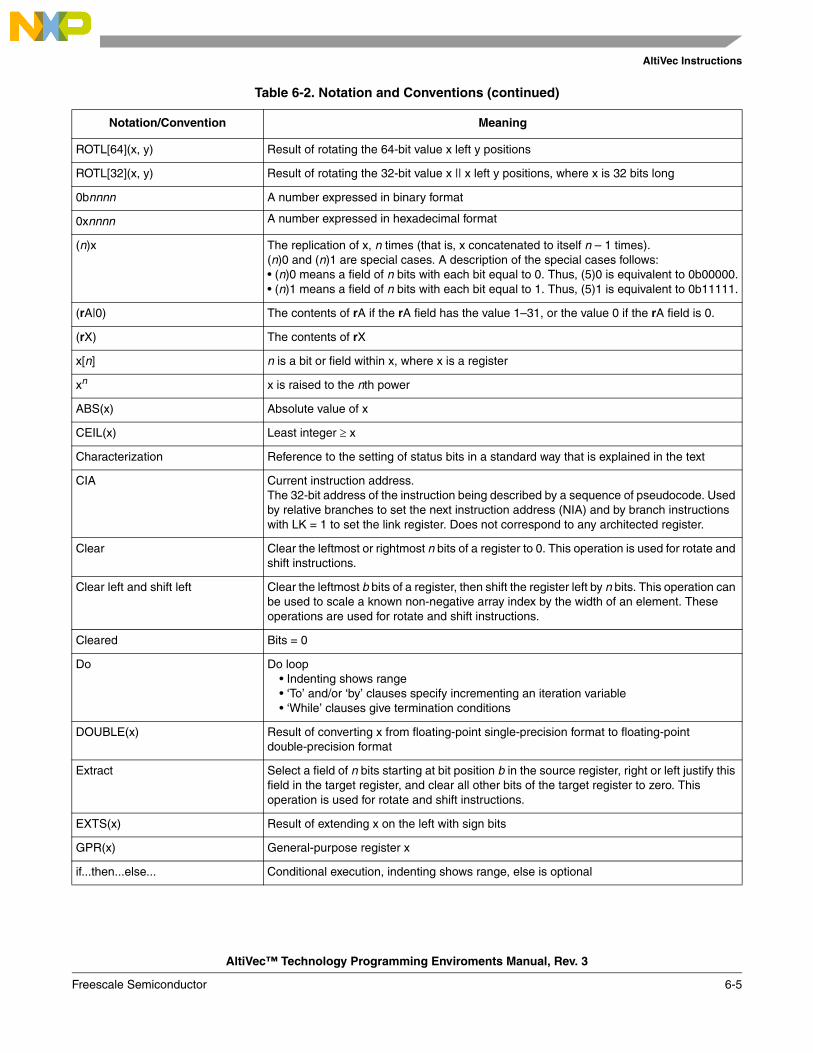
AltiVec Instructions
AltiVec™ Technology Programming Enviroments Manual, Rev. 3
Freescale Semiconductor 6-5
ROTL[64](x, y) Result of rotating the 64-bit value x left y positions
ROTL[32](x, y) Result of rotating the 32-bit value x || x left y positions, where x is 32 bits long
0bnnnn A number expressed in binary format
0xnnnn A number expressed in hexadecimal format
(n)x The replication of x, n times (that is, x concatenated to itself n – 1 times).(n)0 and (n)1 are special cases. A description of the special cases follows:• (n)0 means a field of n bits with each bit equal to 0. Thus, (5)0 is equivalent to 0b00000.• (n)1 means a field of n bits with each bit equal to 1. Thus, (5)1 is equivalent to 0b11111.
(rA|0) The contents of rA if the rA field has the value 1–31, or the value 0 if the rA field is 0.
(rX) The contents of rX
x[n] n is a bit or field within x, where x is a register
xn x is raised to the nth power
ABS(x) Absolute value of x
CEIL(x) Least integer ≥ x
Characterization Reference to the setting of status bits in a standard way that is explained in the text
CIA Current instruction address.The 32-bit address of the instruction being described by a sequence of pseudocode. Used by relative branches to set the next instruction address (NIA) and by branch instructions with LK = 1 to set the link register. Does not correspond to any architected register.
Clear Clear the leftmost or rightmost n bits of a register to 0. This operation is used for rotate and shift instructions.
Clear left and shift left Clear the leftmost b bits of a register, then shift the register left by n bits. This operation can be used to scale a known non-negative array index by the width of an element. These operations are used for rotate and shift instructions.
Cleared Bits = 0
Do Do loop• Indenting shows range • ‘To’ and/or ‘by’ clauses specify incrementing an iteration variable• ‘While’ clauses give termination conditions
DOUBLE(x) Result of converting x from floating-point single-precision format to floating-point double-precision format
Extract Select a field of n bits starting at bit position b in the source register, right or left justify this field in the target register, and clear all other bits of the target register to zero. This operation is used for rotate and shift instructions.
EXTS(x) Result of extending x on the left with sign bits
GPR(x) General-purpose register x
if...then...else... Conditional execution, indenting shows range, else is optional
Table 6-2. Notation and Conventions (continued)
Notation/Convention Meaning
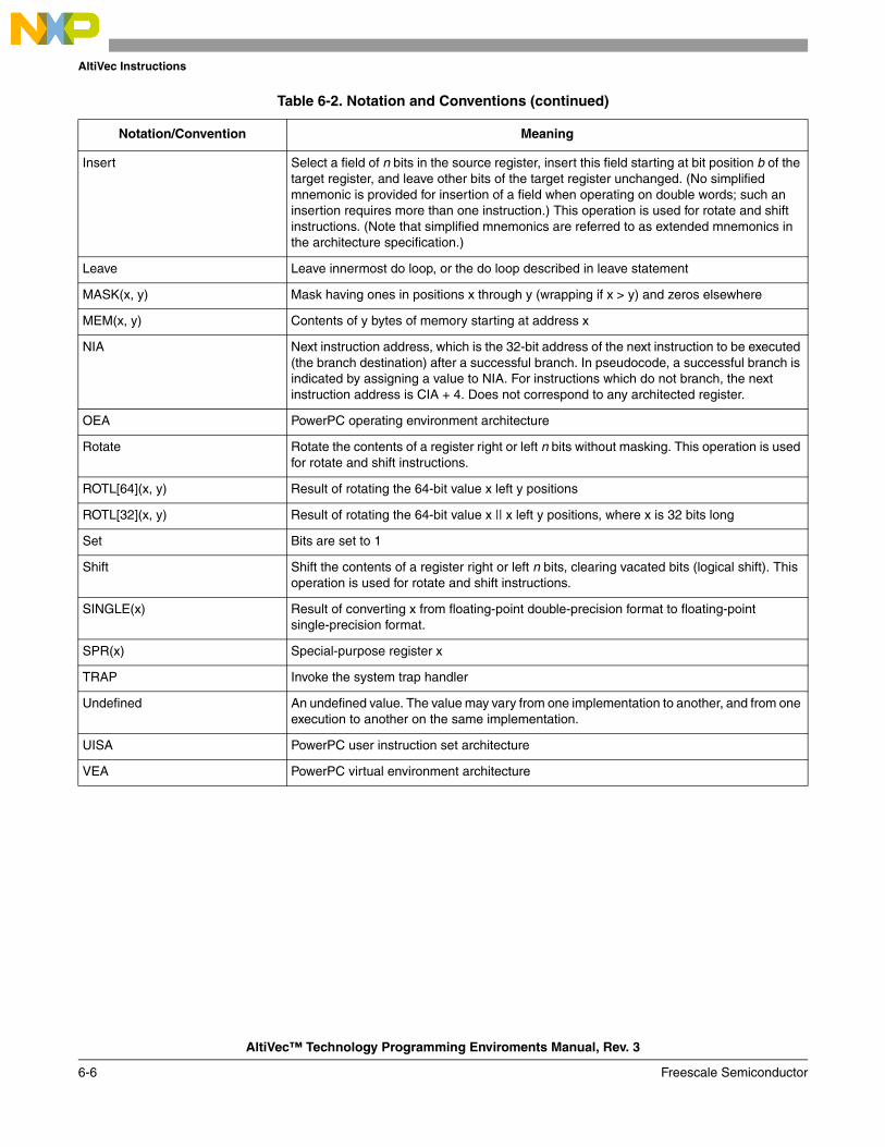
AltiVec Instructions
AltiVec™ Technology Programming Enviroments Manual, Rev. 3
6-6 Freescale Semiconductor
Insert Select a field of n bits in the source register, insert this field starting at bit position b of the target register, and leave other bits of the target register unchanged. (No simplified mnemonic is provided for insertion of a field when operating on double words; such an insertion requires more than one instruction.) This operation is used for rotate and shift instructions. (Note that simplified mnemonics are referred to as extended mnemonics in the architecture specification.)
Leave Leave innermost do loop, or the do loop described in leave statement
MASK(x, y) Mask having ones in positions x through y (wrapping if x > y) and zeros elsewhere
MEM(x, y) Contents of y bytes of memory starting at address x
NIA Next instruction address, which is the 32-bit address of the next instruction to be executed (the branch destination) after a successful branch. In pseudocode, a successful branch is indicated by assigning a value to NIA. For instructions which do not branch, the next instruction address is CIA + 4. Does not correspond to any architected register.
OEA PowerPC operating environment architecture
Rotate Rotate the contents of a register right or left n bits without masking. This operation is used for rotate and shift instructions.
ROTL[64](x, y) Result of rotating the 64-bit value x left y positions
ROTL[32](x, y) Result of rotating the 64-bit value x || x left y positions, where x is 32 bits long
Set Bits are set to 1
Shift Shift the contents of a register right or left n bits, clearing vacated bits (logical shift). This operation is used for rotate and shift instructions.
SINGLE(x) Result of converting x from floating-point double-precision format to floating-point single-precision format.
SPR(x) Special-purpose register x
TRAP Invoke the system trap handler
Undefined An undefined value. The value may vary from one implementation to another, and from one execution to another on the same implementation.
UISA PowerPC user instruction set architecture
VEA PowerPC virtual environment architecture
Table 6-2. Notation and Conventions (continued)
Notation/Convention Meaning

AltiVec Instructions
AltiVec™ Technology Programming Enviroments Manual, Rev. 3
Freescale Semiconductor 6-7
Table 6-3 describes instruction field notation conventions used throughout this chapter.
Precedence rules for pseudocode operators are summarized in Table 6-4.
Operators higher in Table 6-4 are applied before those lower in the table. Operators at the same level in the table associate from left to right, from right to left, or not at all, as shown in the Associativity column. For example, ‘–’ (unary minus) associates from left to right, so a – b – c = (a – b) – c. Parentheses are used to override the evaluation order implied by Table 6-4, or to increase clarity; parenthesized expressions are evaluated before serving as operands.
6.2 AltiVec Instruction SetThe remainder of this chapter lists and describes the instruction set for the AltiVec architecture. The instructions are listed in alphabetical order by mnemonic. The following diagram shows the format for each instruction description page.
Table 6-3. Instruction Field Conventions
PowerPC Architecture Specification
Equivalent in AltiVec Technology PEM as:
RA, RB, RT, RS rA, rB, rD, rS
SI SIMM
U IMM
UI UIMM
VA, VB, VC, VT, VS vA, vB, vC, vD, vS
/, //, /// 0...0 (shaded)
Table 6-4. Precedence Rules
Operators Associativity
x[n], function evaluation Left to right
(n)x or replication, x(n) or exponentiation
Right to left
unary –, ¬ Right to left
∗, ÷ Left to right
+, – Left to right
|| Left to right
=, ≠, <, ≤, >, ≥, <U, >U, ? Left to right
&, ⊕, ≡ Left to right
| Left to right
– (range), : (range) None
←, ←iea None

AltiVec Instructions
AltiVec™ Technology Programming Enviroments Manual, Rev. 3
6-8 Freescale Semiconductor
vaddsbs vaddsbsVector Add Signed Byte Saturate
vaddsbs vD,vA,vB Form VX
do i=0 to 127 by 8
aop0:8 ← SignExtend((vA)i:i+7,9)bop0:8 ← SignExtend((vB)i:i+7,9)temp0:8← aop0:8 +int bop0:8vDi:i+7 ← SItoSIsat(temp0:8,8)
end
Each element of vaddsbs is a byte.
Each signed-integer element in vA is added to the corresponding signed-integer elementin vB.
If the sum is greater than (27-1) it saturates to (27-1) and if it is less than -27 it saturates to -27. If saturations occurs, the SAT bit is set.
The signed-integer result is placed into the corresponding element of vD.
Other registers altered:
Vector status and control register (VSCR):Affected: SAT
Figure 6-11 shows the usage of the vaddsbs instruction. Each of the sixteen elements in the vectors, vA, vB, andvD, is 8 bits long.
Figure 6-11. vaddsbs—Add Saturating Sixteen Signed Integer Elements (8-Bit)
04 vD vA vB 768
0 5 6 10 11 15 16 20 21 25 26 27 28 31
+ +++++++++++++++
vA
vB
vD
Instruction name
Instruction syntax and form
Instruction encodingin decimal
Pseudocode description of instruction operation
Text description ofinstruction operation
Figure showing instruction usage
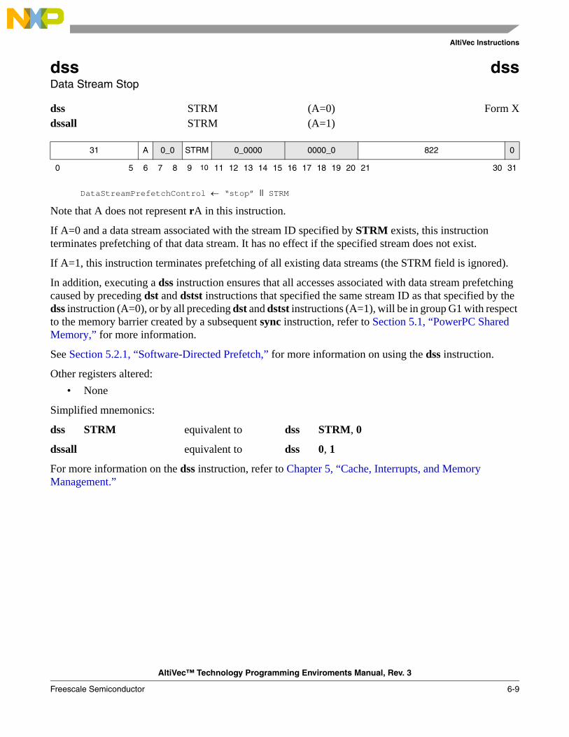
AltiVec Instructions
AltiVec™ Technology Programming Enviroments Manual, Rev. 3
Freescale Semiconductor 6-9
dss dssData Stream Stop
dss STRM (A=0) Form Xdssall STRM (A=1)
DataStreamPrefetchControl ← “stop” || STRM
Note that A does not represent rA in this instruction.
If A=0 and a data stream associated with the stream ID specified by STRM exists, this instruction terminates prefetching of that data stream. It has no effect if the specified stream does not exist.
If A=1, this instruction terminates prefetching of all existing data streams (the STRM field is ignored).
In addition, executing a dss instruction ensures that all accesses associated with data stream prefetching caused by preceding dst and dstst instructions that specified the same stream ID as that specified by the dss instruction (A=0), or by all preceding dst and dstst instructions (A=1), will be in group G1 with respect to the memory barrier created by a subsequent sync instruction, refer to Section 5.1, “PowerPC Shared Memory,” for more information.
See Section 5.2.1, “Software-Directed Prefetch,” for more information on using the dss instruction.
Other registers altered: • None
Simplified mnemonics:
dss STRM equivalent to dss STRM, 0
dssall equivalent to dss 0, 1
For more information on the dss instruction, refer to Chapter 5, “Cache, Interrupts, and Memory Management.”
31 A 0_0 STRM 0_0000 0000_0 822 0
0 5 6 7 8 9 10 11 12 13 14 15 16 17 18 19 20 21 30 31

AltiVec Instructions
AltiVec™ Technology Programming Enviroments Manual, Rev. 3
6-10 Freescale Semiconductor
dst dstData Stream Touch
dst rA,rB,STRM (T=0) Form Xdstt rA,rB,STRM (T=1)
addr0:63 ← (rA)DataStreamPrefetchControl ← “start” || STRM || T || (rB) || addr
This instruction initiates a software directed cache prefetch. The instruction is a hint to hardware that performance will probably be improved if the cache blocks containing the specified data stream are fetched into the data cache because the program will probably soon load from the stream.
The instruction associates the data stream specified by the contents of rA and rB with the stream ID specified by STRM. The instruction defines a data stream STRM as starting at an effective address (rA) and having count units of size quad words separated by stride bytes (as specified in rB). The T bit of the instruction indicates whether the data stream is likely to be loaded from fairly frequently in the near future (T=0) or to be transient and referenced very few times (T=1).
The dst instruction does the following:• Defines the characteristics of a data stream STRM by the contents of rA and rB• Associates the stream with a specified stream ID, STRM (range for STRM is 0–3)• Indicates that the data in the specified stream STRM starting at the address in rA may soon be
loaded• Indicates whether memory locations within the stream are likely to be needed over a longer period
of time (T=0) or be treated as transient data (T=1)• Terminates prefetching from any stream that was previously associated with the specified stream
ID, STRM.
The specified data stream encoded for 32-bit follows:• Effective address: rA, where rA ≠ 0• Block size: rB[3–7] if rB[3–7] ≠ 0; otherwise 32• Block count: rB[8–15] if rB[8–15] ≠ 0; otherwise 256
31 T 0_0 STRM A B 342 0
0 5 6 7 8 9 10 11 15 16 20 21 30 31
0 1 2 3 4 5
StartingAddress
Block Size
BlockStride
BlockAddrn (n=3)
Memory
Stream
Block Block Block Block Block Block

AltiVec Instructions
AltiVec™ Technology Programming Enviroments Manual, Rev. 3
Freescale Semiconductor 6-11
• Block stride: rB[16–31] if rB[16–31] ≠ 0; otherwise 32768
Other registers altered: • None
Simplified mnemonics:
dst rA,rB,STRM equivalent to dst rA,rB,STRM,0
dstt rA,rB,STRM equivalent to dst rA,rB,STRM,1
For more information on the dst instruction, refer to Chapter 5, “Cache, Interrupts, and Memory Management.”
/// Block Size Block Count Block Stride
0 2 3 7 8 15 16 31
Figure 6-1. Format of rB in dst Instruction (32-Bit)

AltiVec Instructions
AltiVec™ Technology Programming Enviroments Manual, Rev. 3
6-12 Freescale Semiconductor
dstst dststData Stream Touch for Store
dstst rA,rB,STRM (T=0) Form Xdststt rA,rB,STRM (T=1)
addr0:63 ← (rA)DataStreamPrefetchControl ← “start” || T || static || (rB) || addr
This instruction initiates a software directed cache prefetch. The instruction is a hint to hardware that performance will probably be improved if the cache blocks containing the specified data stream are fetched into the data cache because the program will probably soon write to (store into) the stream.
The instruction associates the data stream specified by the contents of rA and rB with the stream ID specified by STRM. The instruction defines a data stream STRM as starting at an effective address (rA) and having count units of size quad words separated by stride bytes (as specified in rB). The T bit of the instruction indicates whether the data stream is likely to be stored into fairly frequently in the near future (T=0) or to be transient and referenced very few times (T=1).
The dstst instruction does the following:• Defines the characteristics of a data stream STRM by the contents of rA and rB• Associates the stream with a specified stream ID, STRM (range for STRM is 0–3)• Indicates that the data in the specified stream STRM starting at the address in rA may soon be
stored in to memory• Indicates whether memory locations within the stream are likely to be stored into fairly frequently
in the near future (T=0) or be treated as transient data (T=1)• Terminates prefetching from any stream that was previously associated with the specified stream
ID, STRM.
The specified data stream encoded for 32-bit follows:• Effective address: rA, where rA ≠ 0• Block size: rB[3–7] if rB[3–7] ≠ 0; otherwise 32• Block count: rB[8–15] if rB[8–15] ≠ 0; otherwise 256
31 T 0_0 STRM A B 374 0
0 5 6 7 8 9 10 11 15 16 20 21 30 31
0 1 2 3 4 5
StartingAddress
Block Size
BlockStride
BlockAddrn (n=3)
Memory
Stream
Block Block Block Block Block Block

AltiVec Instructions
AltiVec™ Technology Programming Enviroments Manual, Rev. 3
Freescale Semiconductor 6-13
• Block stride: rB[16–31] if rB[16–31] ≠ 0; otherwise 32768
Other registers altered: • None
Simplified mnemonics:
dstst rA,rB,STRM equivalent to dstst rA,rB,STRM,0
dststt rA,rB,STRM equivalent to dstst rA,rB,STRM,1
For more information on the dstst instruction, refer to Chapter 5, “Cache, Interrupts, and Memory Management.”
/// Block Size Block Count Block Stride
0 2 3 7 8 15 16 31
Figure 6-2. Format of rB in dst Instruction (32-Bit)
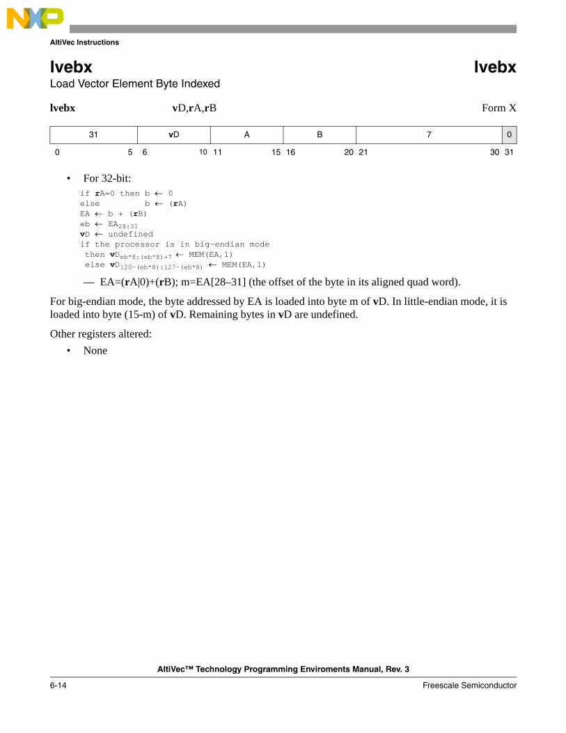
AltiVec Instructions
AltiVec™ Technology Programming Enviroments Manual, Rev. 3
6-14 Freescale Semiconductor
lvebx lvebx Load Vector Element Byte Indexed
lvebx vD,rA,rB Form X
• For 32-bit:if rA=0 then b ← 0else b ← (rA)EA ← b + (rB)eb ← EA28:31vD ← undefinedif the processor is in big-endian mode then vDeb*8:(eb*8)+7 ← MEM(EA,1) else vD120-(eb*8):127-(eb*8) ← MEM(EA,1)
— EA=(rA|0)+(rB); m=EA[28–31] (the offset of the byte in its aligned quad word).
For big-endian mode, the byte addressed by EA is loaded into byte m of vD. In little-endian mode, it is loaded into byte (15-m) of vD. Remaining bytes in vD are undefined.
Other registers altered: • None
31 vD A B 7 0
0 5 6 10 11 15 16 20 21 30 31

AltiVec Instructions
AltiVec™ Technology Programming Enviroments Manual, Rev. 3
Freescale Semiconductor 6-15
Figure 6-3. Effects of Example Load/Store Instructions
x x x x x x x x x x x x x x x x x x x x x x x x x x x x
x x x x x x x x x x x x x x x x x x x x
x x x x x x x x
x x x x x x x x x x x x x x x x x x x x x x x x x x x x
x x x x x x x x x x x x x x x x x x x x x x x x x x x x x x x x
x x x x x x x x x x x x x x x x x x x x x x x x x x x x x x x x
x x x x x x x x x x x x x x x x x x x x x x x x x x x x x x x x
x x x x x x x x x x x x x x x x x x x x x x x x x x x x x x x x
x x x x x x x x x x x x x x x x x x x x x x x x x x x x x x x x
x x x x x x x x x x x x x x x x x x x x x x x x x x x x x x x x
x x x x x x x x x x x x x x x x x x x x x x x x x x x x x x x x
x x x x x x x x x x x x x x x x x x x x x x x x x x x x x x x x0x0000_0000
0x0000_0010
0x0000_0020
0x0000_0030
0x0000_0040
0x0000_0050
0x0000_0060
0x0000_0070
0x0000_0080
0x0000_0090
0x0000_00A0
0x0000_00B0
Byte at x1E
Half at x2A
Word at x54
Quad at A0
vR
vR
vR
vR
Load or Store:
Memory
x x x x x x x x x x x x x x x x x x x x x x x x
x x x x x x x x x x x x x x x x x x x x x x x x x x x x
x x
Note:In vector registers, x means boundedly undefined after a load and don’t care after a store. In memory, x means don’t care after a load, and leave at current value after a store.
x x
x x x x x x x x x x x x x x x x
x x x x x x x x

AltiVec Instructions
AltiVec™ Technology Programming Enviroments Manual, Rev. 3
6-16 Freescale Semiconductor
lvehx lvehx Load Vector Element Half Word Indexed
lvehx vD,rA,rB Form X
• For 32-bit:if rA=0 then b ← 0else b ← (rA)EA ← (b + (rB)) & (~1)eb ← EA28:31vD ← undefinedif the processor is in big-endian mode then vD(eb*8):(eb*8)+15 ← MEM(EA,2) else vD112-(eb*8):127-(eb*8) ← MEM(EA,2)
— Let the EA be the result of ANDing the sum (rA|0)+(rB) with ~1. Let m=EA[28–30]; m is the half word offset of the half word in its aligned quad word in memory.
If the processor is in big-endian mode, the half word addressed by EA is loaded into half word m of vD. If the processor is in little-endian mode, the half word addressed by EA is loaded into half word (7-m) of vD. The remaining half words in vD are set to undefined values. Figure 6-3 shows this instruction.
Other registers altered: • None
31 vD A B 39 0
0 5 6 10 11 15 16 20 21 30 31
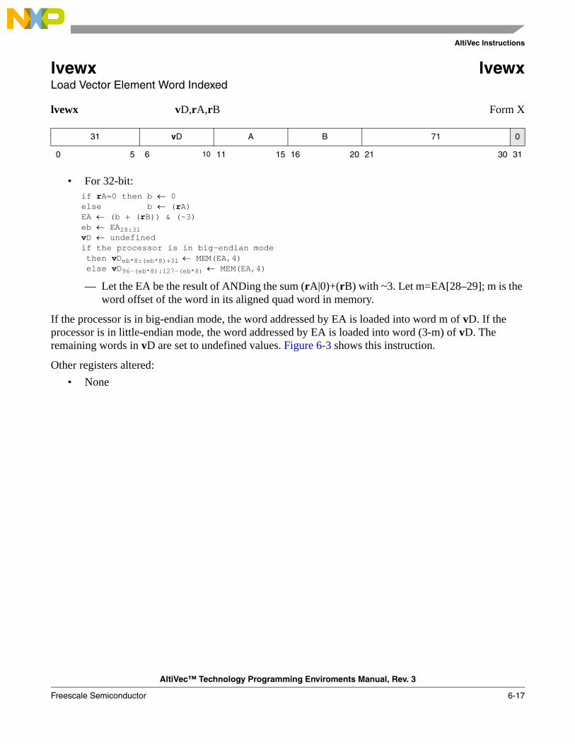
AltiVec Instructions
AltiVec™ Technology Programming Enviroments Manual, Rev. 3
Freescale Semiconductor 6-17
lvewx lvewx Load Vector Element Word Indexed
lvewx vD,rA,rB Form X
• For 32-bit:if rA=0 then b ← 0else b ← (rA)EA ← (b + (rB)) & (~3)eb ← EA28:31vD ← undefinedif the processor is in big-endian mode then vDeb*8:(eb*8)+31 ← MEM(EA,4) else vD96-(eb*8):127-(eb*8) ← MEM(EA,4)
— Let the EA be the result of ANDing the sum (rA|0)+(rB) with ~3. Let m=EA[28–29]; m is the word offset of the word in its aligned quad word in memory.
If the processor is in big-endian mode, the word addressed by EA is loaded into word m of vD. If the processor is in little-endian mode, the word addressed by EA is loaded into word (3-m) of vD. The remaining words in vD are set to undefined values. Figure 6-3 shows this instruction.
Other registers altered: • None
31 vD A B 71 0
0 5 6 10 11 15 16 20 21 30 31

AltiVec Instructions
AltiVec™ Technology Programming Enviroments Manual, Rev. 3
6-18 Freescale Semiconductor
lvsl lvslLoad Vector for Shift Left
lvsl vD,rA,rB Form X
• For 32-bit:if rA = 0 then b ← 0 else b ← (rA)addr0:31 ← b + (rB)sh ← addr28-31if sh = 0x0 then (vD)0:127 ← 0x000102030405060708090A0B0C0D0E0Fif sh = 0x1 then (vD)0:127 ← 0x0102030405060708090A0B0C0D0E0F10if sh = 0x2 then (vD)0:127 ← 0x02030405060708090A0B0C0D0E0F1011if sh = 0x3 then (vD)0:127 ← 0x030405060708090A0B0C0D0E0F101112if sh = 0x4 then (vD)0:127 ← 0x0405060708090A0B0C0D0E0F10111213if sh = 0x5 then (vD)0:127 ← 0x05060708090A0B0C0D0E0F1011121314if sh = 0x6 then (vD)0:127 ← 0x060708090A0B0C0D0E0F101112131415if sh = 0x7 then (vD)0:127 ← 0x0708090A0B0C0D0E0F10111213141516if sh = 0x8 then (vD)0:127 ← 0x08090A0B0C0D0E0F1011121314151617if sh = 0x9 then (vD)0:127 ← 0x090A0B0C0D0E0F101112131415161718if sh = 0xA then (vD)0:127 ← 0x0A0B0C0D0E0F10111213141516171819if sh = 0xB then (vD)0:127 ← 0x0B0C0D0E0F101112131415161718191Aif sh = 0xC then (vD)0:127 ← 0x0C0D0E0F101112131415161718191A1Bif sh = 0xD then (vD)0:127 ← 0x0D0E0F101112131415161718191A1B1Cif sh = 0xE then (vD)0:127 ← 0x0E0F101112131415161718191A1B1C1Dif sh = 0xF then (vD)0:127 ← 0x0F101112131415161718191A1B1C1D1E
— Let the EA be the sum (rA|0)+(rB). Let sh=EA[28–31].
Let X be the 32-byte value 0x00 || 0x01 || 0x02 || ... || 0x1E || 0x1F. Bytes sh:sh+15 of X are placed into vD. Figure 6-4 shows how this instruction works.
Other registers altered: • None
Figure 6-4. Load Vector for Shift Left
The above lvsl instruction followed by a Vector Permute (vperm) would do a simulated alignment of a four-element floating-point vector misaligned on quad-word boundary at address 0x0....C.
31 vD A B 6 0
0 5 6 10 11 15 16 20 21 30 31
0C 0D 0E 0F 10 11 12 13 14 15 16 17 18 19 1A 1B
rA0 0 0 0 0 0 0 8
rB
Temp
vD
0 0 0 0 0 0 0 4
0 0 0 0 0 0 0 CTable Lookup
+
=
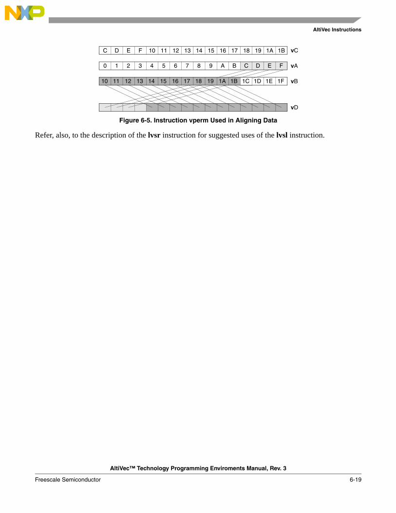
AltiVec Instructions
AltiVec™ Technology Programming Enviroments Manual, Rev. 3
Freescale Semiconductor 6-19
Figure 6-5. Instruction vperm Used in Aligning Data
Refer, also, to the description of the lvsr instruction for suggested uses of the lvsl instruction.
vCC D E F 10 11 12 13 14 15 16 17 18 19 1A 1B
vA
vB
vD
0 1 2 3 4 5 6 7 8 9 A B C D E F
10 11 12 13 14 15 16 17 18 19 1A 1B 1C 1D 1E 1F

AltiVec Instructions
AltiVec™ Technology Programming Enviroments Manual, Rev. 3
6-20 Freescale Semiconductor
lvsr lvsrLoad Vector for Shift Right
lvsr vD,rA,rB Form X
• For 32-bit:if rA = 0 then b ← 0else b ← (rA)EA ← b + (rB)sh ← EA28:31if sh=0x0 then vD ← 0x101112131415161718191A1B1C1D1E1Fif sh=0x1 then vD ← 0x0F101112131415161718191A1B1C1D1Eif sh=0x2 then vD ← 0x0E0F101112131415161718191A1B1C1Dif sh=0x3 then vD ← 0x0D0E0F101112131415161718191A1B1Cif sh=0x4 then vD ← 0x0C0D0E0F101112131415161718191A1Bif sh=0x5 then vD ← 0x0B0C0D0E0F101112131415161718191Aif sh=0x6 then vD ← 0x0A0B0C0D0E0F10111213141516171819if sh=0x7 then vD ← 0x090A0B0C0D0E0F101112131415161718if sh=0x8 then vD ← 0x08090A0B0C0D0E0F1011121314151617if sh=0x9 then vD ← 0x0708090A0B0C0D0E0F10111213141516if sh=0xA then vD ← 0x060708090A0B0C0D0E0F101112131415if sh=0xB then vD ← 0x05060708090A0B0C0D0E0F1011121314if sh=0xC then vD ← 0x0405060708090A0B0C0D0E0F10111213if sh=0xD then vD ← 0x030405060708090A0B0C0D0E0F101112if sh=0xE then vD ← 0x02030405060708090A0B0C0D0E0F1011if sh=0xF then vD ← 0x0102030405060708090A0B0C0D0E0F10
— Let the EA be the sum (rA|0)+(rB). Let sh=EA[28–31]. Let X be the 32-byte value 0x00 || 0x01 || 0x02 || ... || 0x1E || 0x1F. Bytes (16-sh):(31-sh) of X are placed into vD.Note that lvsl and lvsr can be used to create the permute control vector to be used by a subsequent vperm instruction. Let X and Y be the contents of vA and vB specified by the vperm. The control vector created by lvsl causes the vperm to select the high-order 16 bytes of the result of shifting the 32-byte value X || Y left by sh bytes. The control vector created by vsr causes the vperm to select the low-order 16 bytes of the result of shifting X || Y right by sh bytes.These instructions can also be used to rotate or shift the contents of a vector register by sh bytes. For rotating, the vector register to be rotated should be specified as both vA and vB for vperm. For shifting left, the vB register for vperm should contain all zeros and vA should contain the value to be shifted, and vice versa for shifting right. Figure 6-4 shows a similar instruction only in that figure the shift is to the left.No other registers altered.
31 vD A B 38 0
0 5 6 10 11 15 16 20 21 30 31

AltiVec Instructions
AltiVec™ Technology Programming Enviroments Manual, Rev. 3
Freescale Semiconductor 6-21
lvx lvxLoad Vector Indexed
lvx vD,rA,rB (LRU=0) Form X
• For 32-bit:if rA=0 then b ← 0else b ← (rA)EA ← (b + (rB)) & (~0xF)if the processor is in big-endian mode then vD ← MEM(EA,16) else vD ← MEM(EA+8,8) || MEM(EA,8)
Let the EA be the result of ANDing the sum (rA|0)+(rB) with ~0xF.
If the processor is in big-endian mode, the quad word in memory addressed by EA is loaded into vD.
If the processor is in little-endian mode, the doubleword addressed by EA is loaded into vD[64–127] and the doubleword addressed by EA+8 is loaded into vD[0–63]. Note that normal little-endian PowerPC address swizzling is also performed. See Section 3.1, “Data Organization in Memory,” for more information.
Figure 6-4 shows this instruction.
Other registers altered: • None
31 vD A B 103 0
0 5 6 10 11 15 16 20 21 30 31

AltiVec Instructions
AltiVec™ Technology Programming Enviroments Manual, Rev. 3
6-22 Freescale Semiconductor
lvxl lvxlLoad Vector Indexed LRU
lvxl vD,rA,rB (LRU=1) Form X
• For 32-bit:if rA=0 then b ← 0else b ← (rA)EA ← (b + (rB)) & (~0xF)if the processor is in big-endian mode then vD ← MEM(EA,16) else vD ← MEM(EA+8,8) || MEM(EA,8)
Let the EA be the result of ANDing the sum (rA|0)+(rB) with ~0xF.
If the processor is in big-endian mode, the quad word addressed by EA is loaded into vD.
If the processor is in little-endian mode, the doubleword addressed by EA is loaded into vD[64–127] and the doubleword addressed by EA+8 is loaded into vD[0–63]. Note that normal little-endian PowerPC address swizzling is also performed. See Section 3.1, “Data Organization in Memory,” for more information.
lvxl provides a hint that the program may not need quad word addressed by EA again soon.
Note that on some implementations, the hint provided by the lvxl instruction and the corresponding hint provided by the Store Vector Indexed LRU (stvxl) instruction (see Section 5.2.1.2, “Transient Streams”) are applied to the entire cache block containing the specified quad word. On such implementations, the effect of the hint may be to cause that cache block to be considered a likely candidate for reuse when space is needed in the cache for a new block. Thus, on such implementations, the hint should be used with caution if the cache block containing the quad word also contains data that may be needed by the program in the near future. Also, the hint may be used before the last reference in a sequence of references to the quad word if the subsequent references are likely to occur sufficiently soon that the cache block containing the quad word is not likely to be displaced from the cache before the last reference. Figure 6-4 shows this instruction.
Other registers altered: • None
31 vD A B 359 0
0 5 6 10 11 15 16 20 21 30 31

AltiVec Instructions
AltiVec™ Technology Programming Enviroments Manual, Rev. 3
Freescale Semiconductor 6-23
mfvscr mfvscrMove from Vector Status and Control Register
mfvscr vD Form VX
vD ← 960 || (VSCR)
The contents of the VSCR are placed into vD.
Note that the programmer should assume that mtvscr and mfvscr take substantially longer to execute than other AltiVec instructions
Other registers altered: • None
04 vD 0_0000 0000_0 1540
0 5 6 10 11 15 16 20 21 31

AltiVec Instructions
AltiVec™ Technology Programming Enviroments Manual, Rev. 3
6-24 Freescale Semiconductor
mtvscr mtvscrMove to Vector Status and Control Register
mtvscr vB Form VX
VSCR ← (vB)96:127
The contents of vB are placed into the VSCR.
Other registers altered: • None
04 00_000 0_0000 vB 1604
0 5 6 10 11 15 16 20 21 31

AltiVec Instructions
AltiVec™ Technology Programming Enviroments Manual, Rev. 3
Freescale Semiconductor 6-25
stvebx stvebxStore Vector Element Byte Indexed
stvebx vS,rA,rB Form X
• For 32-bit:if rA=0 then b ← 0else b ← (rA)EA ← b + (rB)eb ← EA28:31if the processor is in big-endian mode then MEM(EA,1) ← (vS)eb*8:(eb*8)+7 else MEM(EA,1) ← (vS)120-(eb*8):127-eb*8
— Let the EA be the sum (rA|0)+(rB). Let m=EA[28–31]; m is the byte offset of the byte in its aligned quad word in memory.
If the processor is in big-endian mode, byte m of vS is stored into the byte in memory addressed by EA. If the processor is in little-endian mode, byte (15-m) of vS is stored into the byte addressed by EA. Figure 6-3 shows how a store instruction is performed for a vector register.
Other registers altered: • None
31 vS A B 135 0
0 5 6 10 11 15 16 20 21 30 31

AltiVec Instructions
AltiVec™ Technology Programming Enviroments Manual, Rev. 3
6-26 Freescale Semiconductor
stvehx stvehxStore Vector Element Half Word Indexed
stvehx vS,rA,rB Form X
• For 32-bit:if rA=0 then b ← 0else b ← (rA)EA ← (b + (rB)) & (~0x1)eb ← EA28:31if the processor is in big-endian mode then MEM(EA,2) ← (vS)eb*8:(eb*8)+15 else MEM(EA,2) ← (vS)112-eb*8:127-(eb*8)
— Let the EA be the result of ANDing the sum (rA|0)+(rB) with ~0x1. Let m=EA[28–30]; m is the half word offset of the half word in its aligned quad word in memory.
If the processor is in big-endian mode, half word m of vS is stored into the half word addressed by EA. If the processor is in little-endian mode, half word (7-m) of vS is stored into the half word addressed by EA. Figure 6-3 shows how a store instruction is performed for a vector register.
Other registers altered: • None
31 vS A B 167 0
0 5 6 10 11 15 16 20 21 30 31

AltiVec Instructions
AltiVec™ Technology Programming Enviroments Manual, Rev. 3
Freescale Semiconductor 6-27
stvewx stvewxStore Vector Element Word Indexed
stvewx vS,rA,rB Form X
• For 32-bit:if rA=0 then b ← 0else b ← (rA)EA ← (b + (rB)) & 0xFFFF_FFFCeb ← EA28:31if the processor is in big-endian mode then MEM(EA,4) ← (vS)eb*8:(eb*8)+31 else MEM(EA,4) ← (vS)96-eb*8:127-(eb*8)
— Let the EA be the result of ANDing the sum (rA|0)+(rB) with 0xFFFF_FFFC. Let m=EA[28–29]; m is the word offset of the word in its aligned quad word in memory.
If the processor is in big-endian mode, word m of vS is stored into the word addressed by EA. If the processor is in little-endian mode, word (3-m) of vS is stored into the word addressed by EA. Figure 6-3 shows how a store instruction is performed for a vector register.
Other registers altered: • None
31 vS A B 199 0
0 5 6 10 11 15 16 20 21 30 31

AltiVec Instructions
AltiVec™ Technology Programming Enviroments Manual, Rev. 3
6-28 Freescale Semiconductor
stvx stvxStore Vector Indexed
stvx vS,rA,rB (LRU=0) Form X
• For 32-bit:if rA=0 then b ← 0else b ← (rA)EA ← (b + (rB)) & 0xFFFF_FFF0if the processor is in big-endian mode then MEM(EA,16) ← (vS) else MEM(EA,16) ← (vS)64:127 || (vS)0:63
— Let the EA be the result of ANDing the sum (rA|0)+(rB) with 0xFFFF_FFF0.
If the processor is in big-endian mode, the contents of vS are stored into the quad word addressed by EA. If the processor is in little-endian mode, the contents of vS[64–127] are stored into the doubleword addressed by EA, and the contents of vS[0–63] are stored into the doubleword addressed by EA+8.
stvxl and stvxlt provide a hint that the quad word addressed by EA will probably not be needed again by the program in the near future.
Figure 6-3 shows how a store instruction is performed for a vector register.
Other registers altered: • None
31 vS A B 231 0
0 5 6 10 11 15 16 20 21 30 31

AltiVec Instructions
AltiVec™ Technology Programming Enviroments Manual, Rev. 3
Freescale Semiconductor 6-29
stvxl stvxlStore Vector Indexed LRU
stvxl vS,rA,rB (LRU=1) Form X
• For 32-bit:if rA=0 then b ← 0else b ← (rA)EA ← (b + (rB)) & 0xFFFF_FFF0if the processor is in big-endian mode then MEM(EA,16) ← (vS) else MEM(EA,16) ← (vS)64:127 || (vS)0:63
— Let the EA be the result of ANDing the sum (rA|0)+(rB) with 0xFFFF_FFF0.
Let the EA be the result of ANDing the sum (rA|0)+(rB) with 0xFFFF_FFFF_FFFF_FFF0. If the processor is in big-endian mode, the contents of vS are stored into the quad word addressed by EA. If the processor is in little-endian mode, the contents of vS[64–127] are stored into the doubleword addressed by EA, and the contents of vS[0–63] are stored into the doubleword addressed by EA+8. The stvxl and stvxlt instructions provide a hint that the quad word addressed by EA will probably not be needed again by the program in the near future.
Note that on some implementations, the hint provided by the stvxl instruction (see Section 5.2.2, “Prioritizing Cache Block Replacement”) is applied to the entire cache block containing the specified quad word. On such implementations, the effect of the hint may be to cause that cache block to be considered a likely candidate for reuse when space is needed in the cache for a new block. Thus, on such implementations, the hint should be used with caution if the cache block containing the quad word also contains data that may be needed by the program in the near future. Also, the hint may be used before the last reference in a sequence of references to the quad word if the subsequent references are likely to occur sufficiently soon that the cache block containing the quad word is not likely to be displaced from the cache before the last reference. Figure 6-3 shows how a store instruction is performed on the vector registers.Other registers altered:
• None
31 vS A B 487 0
0 5 6 10 11 15 16 20 21 30 31

AltiVec Instructions
AltiVec™ Technology Programming Enviroments Manual, Rev. 3
6-30 Freescale Semiconductor
vaddcuw vaddcuwVector Add Carryout Unsigned Word
vaddcuw vD,vA,vB Form VX
do i=0 to 127 by 32aop0:32 ← ZeroExtend((vA)i:i+31,33)bop0:32 ← ZeroExtend((vB)i:i+31,33)temp0:32 ← aop0:32 +int bop0:32vDi:i+31 ← ZeroExtend(temp0,32)
end
Each unsigned-integer word element in vA is added to the corresponding unsigned-integer word element in vB. The carry out of bit 0 of the 32-bit sum is zero-extended to 32 bits and placed into the corresponding word element of vD.
Other registers altered: • None
Figure 6-6 shows the usage of the vaddcuw instruction. Each of the four elements in the vectors, vA, vB, and vD, is 32 bits long.
Figure 6-6. vaddcuw—Determine Carries of Four Unsigned Integer Adds (32-Bit)
04 vD vA vB 384
0 5 6 10 11 15 16 20 21 31
vA
vB
33-Bit Intermediate
vD
+ + + +

AltiVec Instructions
AltiVec™ Technology Programming Enviroments Manual, Rev. 3
Freescale Semiconductor 6-31
vaddfp vaddfpVector Add Floating-Point
vaddfp vD,vA,vB Form VX
do i = 0,127,32(vD)i:i+31 ← RndToNearFP32((vA)i:i+31 +fp (vB)i:i+31)
end
The four 32-bit floating-point values in vA are added to the four 32-bit floating-point values in vB. The four intermediate results are rounded and placed in vD.
If VSCR[NJ]=1, every denormalized operand element is truncated to a 0 of the same sign before the operation is carried out, and each denormalized result element truncates to a 0 of the same sign.
Other registers altered: • None
Figure 6-7 shows the usage of the vaddfp instruction. Each of the four elements in the vectors, vA, vB, and vD, is 32 bits long.
Figure 6-7. vaddfp—Add Four Floating-Point Elements (32-Bit)
04 vD vA vB 10
0 5 6 10 11 15 16 20 21 31
++++
vA
vB
vD

AltiVec Instructions
AltiVec™ Technology Programming Enviroments Manual, Rev. 3
6-32 Freescale Semiconductor
vaddsbs vaddsbs Vector Add Signed Byte Saturate
vaddsbs vD,vA,vB Form VX
do i=0 to 127 by 8aop0:8 ← SignExtend((vA)i:i+7,9)bop0:8 ← SignExtend((vB)i:i+7,9)temp0:8 ← aop0:8 +int bop0:8vDi:i+7 ← SItoSIsat(temp0:8,8)
end
Each element of vaddsbs is a byte.
Each signed-integer element in vA is added to the corresponding signed-integer element in vB.
If the sum is greater than (27-1) it saturates to (27-1) and if it is less than -27 it saturates to -27. If saturation occurs, the SAT bit is set.
The signed-integer result is placed into the corresponding element of vD.
Other registers altered:• Vector status and control register (VSCR):
Affected: SAT
Figure 6-8 shows the usage of the vaddsbs instruction. Each of the sixteen elements in the vectors, vA, vB, and vD, is 8 bits long.
Figure 6-8. vaddsbs—Add Saturating Sixteen Signed Integer Elements (8-Bit)
04 vD vA vB 768
0 5 6 10 11 15 16 20 21 31
+ +++++++++++++++
vA
vB
vD

AltiVec Instructions
AltiVec™ Technology Programming Enviroments Manual, Rev. 3
Freescale Semiconductor 6-33
vaddshs vaddshs Vector Add Signed Half Word Saturate
vaddshs vD,vA,vB Form VX
do i=0 to 127 by 16aop0:16 ← SignExtend((vA)i:i+15,16)bop0:16 ← SignExtend((vB)i:i+15,16)temp0:16 ← aop0:16 +int bop0:16vDi:i+15 ← SItoSIsat(temp0:16,16)
end
Each element of vaddshs is a half word.
Each signed-integer element in vA is added to the corresponding signed-integer element in vB.
If the sum is greater than (215-1) it saturates to (215-1) and if it is less than -215 it saturates to -215. If saturation occurs, the SAT bit is set.
The signed-integer result is placed into the corresponding element of vD.
Other registers altered:• Vector status and control register (VSCR):
Affected: SAT
Figure 6-9 shows the usage of the vaddshs instruction. Each of the eight elements in the vectors, vA, vB, and vD, is 16 bits long.
Figure 6-9. vaddshs—Add Saturating Eight Signed Integer Elements (16-Bit)
04 vD vA vB 832
0 5 6 10 11 15 16 20 21 31
++++++++
vA
vB
vD

AltiVec Instructions
AltiVec™ Technology Programming Enviroments Manual, Rev. 3
6-34 Freescale Semiconductor
vaddsws vaddsws Vector Add Signed Word Saturate
vaddsws vD,vA,vB Form VX
do i=0 to 127 by 32aop0:32 ← SignExtend((vA)i:i+31,33)bop0:32 ← SignExtend((vB)i:i+31,33)temp0:32 ← aop0:32 +int bop0:32vDi:i+31 ← SItoSIsat(temp0:32,32)
end
Each element of vaddsws is a word.
Each signed-integer element in vA is added to the corresponding signed-integer element in vB.
If the sum is greater than (231-1) it saturates to (231-1) and if it is less than (-231) it saturates to (-231). If saturation occurs, the SAT bit is set.
The signed-integer result is placed into the corresponding element of vD.
Other registers altered:• Vector status and control register (VSCR):
Affected: SAT
Figure 6-10 shows the usage of the vaddsws instruction. Each of the 4 elements in the vectors, vA, vB, and vD, is 32 bits long.
Figure 6-10. vaddsws—Add Saturating Four Signed Integer Elements (32-Bit)
04 vD vA vB 896
0 5 6 10 11 15 16 20 21 31
++++
vA
vB
vD

AltiVec Instructions
AltiVec™ Technology Programming Enviroments Manual, Rev. 3
Freescale Semiconductor 6-35
vaddubm vaddubm Vector Add Unsigned Byte Modulo
vaddubm vD,vA,vB Form VX
do i=0 to 127 by 8vDi:i+7 ← (vA)i:i+7 +int (vB)i:i+7
end
Each element of vaddubm is a byte.
Each integer element in vA is modulo added to the corresponding integer element in vB. The integer result is placed into the corresponding element of vD.
Note that the vaddubm instruction can be used for unsigned or signed integers.
Other registers altered: • None
Figure 6-11 shows the vaddubm instruction usage. Each of the sixteen elements in the vectors, vA, vB, and vD, is 8 bits long.
Figure 6-11. vaddubm—Add Sixteen Integer Elements (8-Bit)
04 vD vA vB 0
0 5 6 10 11 15 16 20 21 31
+ +++++++++++++++
vA
vB
vD

AltiVec Instructions
AltiVec™ Technology Programming Enviroments Manual, Rev. 3
6-36 Freescale Semiconductor
vaddubs vaddubs Vector Add Unsigned Byte Saturate
vaddubs vD,vA,vB Form VX
do i=0 to 127 by 8aop0:8 ← ZeroExtend((vA)i:i+7,9)bop0:8 ← ZeroExtend((vB)i:i+7,9)temp0:8 ← aop0:8 +int bop0:8vDi:i+7 ← UItoUIsat(temp0:8,8)
end
Each element of vaddubs is a byte.
Each unsigned-integer element in vA is added to the corresponding unsigned-integer element in vB.
If the sum is greater than (28-1) it saturates to (28-1) and the SAT bit is set.
The unsigned-integer result is placed into the corresponding element of vD.
Other registers altered:• Vector status and control register (VSCR):
Affected: SAT
Figure 6-12 shows the usage of the vaddubs instruction. Each of the sixteen elements in the vectors, vA, vB, and vD, is 8 bits long.
Figure 6-12. vaddubs—Add Saturating Sixteen Unsigned Integer Elements (8-Bit)
04 vD vA vB 512
0 5 6 10 11 15 16 20 21 31
+ +++++++++++++++
vA
vB
vD

AltiVec Instructions
AltiVec™ Technology Programming Enviroments Manual, Rev. 3
Freescale Semiconductor 6-37
vadduhm vadduhm Vector Add Unsigned Half Word Modulo
vadduhm vD,vA,vB Form VX
do i=0 to 127 by 16vDi:i+15 ← (vA)i:i+15 +int (vB)i:i+15
end
Each element of vadduhm is a half word.
Each integer element in vA is added to the corresponding integer element in vB. The integer result is placed into the corresponding element of vD.
Note that the vadduhm instruction can be used for unsigned or signed integers.
Other registers altered: • None
Figure 6-13 shows the usage of the vadduhm instruction. Each of the eight elements in the vectors, vA, vB, and vD, is 16 bits long.
Figure 6-13. vadduhm—Add Eight Integer Elements (16-Bit)
04 vD vA vB 64
0 5 6 10 11 15 16 20 21 31
++++++++
vA
vB
vD

AltiVec Instructions
AltiVec™ Technology Programming Enviroments Manual, Rev. 3
6-38 Freescale Semiconductor
vadduhs vadduhs Vector Add Unsigned Half Word Saturate
vadduhs vD,vA,vB Form VX
do i=0 to 127 by 16aop0:16 ← ZeroExtend((vA)i:i+15,17)bop0:16 ← ZeroExtend((vB)i:i+15,17)temp0:16 ← aop0:16 +int bop0:16vDi:i+15 ← UItoUIsat(temp0:16,16)
end
Each element of vadduhs is a half word.
Each unsigned-integer element in vA is added to the corresponding unsigned-integer element in vB.
If the sum is greater than (216-1) it saturates to (216-1) and the SAT bit is set.
The unsigned-integer result is placed into the corresponding element of vD.
Other registers altered:• Vector status and control register (VSCR):
Affected: SAT
Figure 6-14 shows the usage of the vadduhs instruction. Each of the eight elements in the vectors, vA, vB, and vD, is 16 bits long.
Figure 6-14. vadduhs—Add Saturating Eight Unsigned Integer Elements (16-Bit)
04 vD vA vB 576
0 5 6 10 11 15 16 20 21 31
++++++++
vA
vB
vD

AltiVec Instructions
AltiVec™ Technology Programming Enviroments Manual, Rev. 3
Freescale Semiconductor 6-39
vadduwm vadduwm Vector Add Unsigned Word Modulo
vadduwm vD,vA,vB Form: VX
do i=0 to 127 by 32vDi:i+31 ← (vA)i:i+31 +int (vB)i:i+31
end
Each element of vadduwm is a word.
Each integer element in vA is modulo added to the corresponding integer element in vB. The integer result is placed into the corresponding element of vD.
Note that the vadduwm instruction can be used for unsigned or signed integers.
Other registers altered: • None
Form:• VX
Figure 6-15 shows the usage of the vadduwm instruction. Each of the four elements in the vectors, vA, vB, and vD, is 32 bits long.
Figure 6-15. vadduwm—Add Four Integer Elements (32-Bit)
04 vD vA vB 128
0 5 6 10 11 15 16 20 21 31
++++
vA
vB
vD

AltiVec Instructions
AltiVec™ Technology Programming Enviroments Manual, Rev. 3
6-40 Freescale Semiconductor
vadduws vadduws Vector Add Unsigned Word Saturate
vadduws vD,vA,vB Form: VX
do i=0 to 127 by 3aop0:32 ← ZeroExtend((vA)i:i+31,33)bop0:32 ← ZeroExtend((vB)i:i+31,33)temp0:32 ← aop0:32 +int bop0:32vDi:i+31 ← UItoUIsat(temp0:32,32)
end
Each element of vadduws is a word.
Each unsigned-integer element in vA is added to the corresponding unsigned-integer element in vB.
If the sum is greater than (232-1) it saturates to (232-1) and the SAT bit is set.
The unsigned-integer result is placed into the corresponding element of vD.
Other registers altered:• Vector status and control register (VSCR):
Affected: SAT
Figure 6-16 shows the usage of the vadduws instruction. Each of the four elements in the vectors, vA, vB, and vD, is 32 bits long.
Figure 6-16. vadduws—Add Saturating Four Unsigned Integer Elements (32-Bit)
04 vD vA vB 640
0 5 6 10 11 15 16 20 21 31
++++
vA
vB
vD

AltiVec Instructions
AltiVec™ Technology Programming Enviroments Manual, Rev. 3
Freescale Semiconductor 6-41
vand vand Vector Logical AND
vand vD,vA,vB Form: VX
vD ← (vA) & (vB)
The contents of vA are bitwise ANDed with the contents of vB and the result is placed into vD.
Other registers altered: • None
Figure 6-17 shows usage of the vand instruction.
Figure 6-17. vand—Logical Bitwise AND
04 vD vA vB 1028
0 5 6 10 11 15 16 20 21 31
&
vA
vB
vD

AltiVec Instructions
AltiVec™ Technology Programming Enviroments Manual, Rev. 3
6-42 Freescale Semiconductor
vandc vandcVector Logical AND with Complement
vandc vD,vA,vB Form: VX
vD ← (vA) & ¬(vB)
The contents of vA are ANDed with the one’s complement of the contents of vB and the result is placed into vD.
Other registers altered: • None
Figure 6-17 shows usage of the vandc instruction.
Figure 6-18. vand—Logical Bitwise AND with Complement
04 vD vA vB 1092
0 5 6 10 11 15 16 20 21 31
&
vB
Intermediate
vA
vD
¬

AltiVec Instructions
AltiVec™ Technology Programming Enviroments Manual, Rev. 3
Freescale Semiconductor 6-43
vavgsb vavgsbVector Average Signed Byte
vavgsb vD,vA,vB Form: VX
do i=0 to 127 by 8aop0:8 ← SignExtend((vA)i:i+7,9)bop0:8 ← SignExtend((vB)i:i+7,9)temp0:8 ← aop0:8 +int bop0:8 +int 1vDi:i+7 ← temp0:7
end
Each element of vavgsb is a byte.
Each signed-integer byte element in vA is added to the corresponding signed-integer byte element in vB, producing a 9-bit signed-integer sum. The sum is incremented by 1. The high-order 8 bits of the result are placed into the corresponding element of vD.
Other registers altered: • None
Figure 6-19 shows the usage of the vavgsb instruction. Each of the sixteen elements in the vectors, vA, vB, and vD, is 8 bits long.
Figure 6-19. vavgsb—Average Sixteen Signed Integer Elements (8-Bit)
04 vD vA vB 1282
0 5 6 10 11 15 16 20 21 31
+ +++++++++++++++
vA
vB
vD
+1 +1+1+1+1+1+1+1+1+1+1+1+1+1+1+1
Temp
Temp
8 Bits
9 Bits

AltiVec Instructions
AltiVec™ Technology Programming Enviroments Manual, Rev. 3
6-44 Freescale Semiconductor
vavgsh vavgshVector Average Signed Half Word
vavgsh vD,vA,vB Form: VX
do i=0 to 127 by 16aop0:16 ← SignExtend((vA)i:i+15,17)bop0:16 ← SignExtend((vB)i:i+15,17)temp0:16 ← aop0:15 +int bop0:15 +int 1vDi:i+15 ← temp0:15
end
Each element of vavgsh is a half word.
Each signed-integer element in vA is added to the corresponding signed-integer element in vB, producing an 17-bit signed-integer sum. The sum is incremented by 1. The high-order 16 bits of the result are placed into the corresponding element of vD.
Other registers altered: • None
Figure 6-20 shows the usage of the vavgsh instruction. Each of the eight elements in the vectors, vA, vB, and vD, is 16 bits long.
Figure 6-20. vavgsh—Average Eight Signed Integer Elements (16-Bit)
04 vD vA vB 1346
0 5 6 10 11 15 16 20 21 31
+++++++
vA
vB
+1+1+1+1+1+1+1
Temp
16 Bits
17 Bits
+
+1
Temp
vD

AltiVec Instructions
AltiVec™ Technology Programming Enviroments Manual, Rev. 3
Freescale Semiconductor 6-45
vavgsw vavgswVector Average Signed Word
vavgsw vD,vA,vB Form: VX
do i=0 to 127 by 32aop0:32 ← SignExtend((vA)i:i+31,33)bop0:3 ← SignExtend((vB)i:i+31,33)temp0:32 ← aop0:32 +int bop0:32 +int 1vDi:i+31 ← temp0:31
end
Each element of vavgsw is a word.
Each signed-integer element in vA is added to the corresponding signed-integer element in vB, producing an 33-bit signed-integer sum. The sum is incremented by 1. The high-order 32 bits of the result are placed into the corresponding element of vD.
Other registers altered: • None
Figure 6-21 shows the usage of the vavgsw instruction. Each of the four elements in the vectors, vA, vB, and vD, is 32 bits long.
Figure 6-21. vavgsw—Average Four Signed Integer Elements (32-Bit)
04 vD vA vB 1410
0 5 6 10 11 15 16 20 21 31
+++
vA
vB
+1+1+1
Temp
32 Bits
33 Bits
+
+1
Temp
vD

AltiVec Instructions
AltiVec™ Technology Programming Enviroments Manual, Rev. 3
6-46 Freescale Semiconductor
vavgub vavgubVector Average Unsigned Byte
vavgub vD,vA,vB Form: VX
do i=0 to 127 by 8aop0:8 ← ZeroExtend((vA)i:i+7,9)bop0:n ← ZeroExtend((vB)i:i+71,9)temp0:n ← aop0:8 +int bop0:8 +int 1vDi:i+7 ← temp0:7
end
Each element of vavgub is a byte.
Each unsigned-integer element in vA is added to the corresponding unsigned-integer element in vB, producing a 9-bit unsigned-integer sum. The sum is incremented by 1. The high-order 8 bits of the result are placed into the corresponding element of vD.
Other registers altered: • None
Figure 6-22 shows the usage of the vavgub instruction. Each of the sixteen elements in the vectors, vA, vB, and vD, is 8 bits long.
.
Figure 6-22. vavgub—Average Sixteen Unsigned Integer Elements (8-Bit)
04 vD vA vB 1026
0 5 6 10 11 15 16 20 21 31
+ +++++++++++++++
vA
vB
vD
+1 +1+1+1+1+1+1+1+1+1+1+1+1+1+1+1
Temp
Temp
8 Bits
9 Bits

AltiVec Instructions
AltiVec™ Technology Programming Enviroments Manual, Rev. 3
Freescale Semiconductor 6-47
vavguh vavguhVector Average Unsigned Half Word
vavguh vD,vA,vB Form: VX
do i=0 to 127 by 16aop0:16 ← ZeroExtend((vA)i:i+15,17)bop0:16 ← ZeroExtend((vB)i:i+15,17)temp0:16 ← aop0:16 +int bop0:16 +int 1vDi:i+15 ← temp0:15
end
Each element of vavguh is a half word.
Each unsigned-integer element in vA is added to the corresponding unsigned-integer element in vB, producing a 17-bit unsigned-integer. The sum is incremented by 1. The high-order 16 bits of the result are placed into the corresponding element of vD.
Other registers altered: • None
Figure 6-23 shows the usage of the vavguh instruction. Each of the eight elements in the vectors, vA, vB, and vD, is 16 bits long.
Figure 6-23. vavguh—Average Eight Signed Integer Elements (16-Bit)
04 vD vA vB 1090
0 5 6 10 11 15 16 20 21 31
+++++++
vA
vB
+1+1+1+1+1+1+1
Temp
16 Bits
17 Bits
+
+1
Temp
vD

AltiVec Instructions
AltiVec™ Technology Programming Enviroments Manual, Rev. 3
6-48 Freescale Semiconductor
vavguw vavguwVector Average Unsigned Word
vavguw vD,vA,vB Form: VX
do i=0 to 127 by 32aop0:32 ← ZeroExtend((vA)i:i+31,33)bop0:32 ← ZeroExtend((vB)i:i+31,33)temp0:32 ← aop0:32 +int bop0:32 +int 1vDi:i+31 ← temp0:31
end
Each element of vavguw is a word.
Each unsigned-integer element in vA is added to the corresponding unsigned-integer element in vB, producing a 33-bit unsigned-integer sum. The sum is incremented by 1. The high-order 32 bits of the result are placed into the corresponding element of vD.
Other registers altered: • None
Figure 6-24 shows the usage of the vavguw instruction. Each of the four elements in the vectors, vA, vB, and vD, is 32 bits long.
Figure 6-24. vavguw—Average Four Unsigned Integer Elements (32-Bit)
04 vD vA vB 1154
0 5 6 10 11 15 16 20 21 31
+++
vA
vB
+1+1+1
Temp
32 Bits
33 Bits
+
+1
Temp
vD

AltiVec Instructions
AltiVec™ Technology Programming Enviroments Manual, Rev. 3
Freescale Semiconductor 6-49
vcfsx vcfsxVector Convert from Signed Fixed-Point Word
vcfsx vD,vB,UIMM Form: VX
do i=0 to 127 by 32vDi:i+31 ← CnvtSI32ToFP32((vB)i:i+31) ÷fp 2
UIMM
end
Each signed fixed-point integer word element in vB is converted to the nearest single-precision floating-point value. The result is divided by 2UIMM (UIMM=Unsigned immediate value) and placed into the corresponding word element of vD.
Other registers altered: • None
Figure 6-25 shows the usage of the vcfsx instruction. Each of the four elements in the vectors, vB and vD, is 32 bits long.
Figure 6-25. vcfsx—Convert Four Signed Integer Elements to Four Floating-Point Elements (32-Bit)
04 vD UIMM vB 842
0 5 6 10 11 15 16 20 21 31
vB
vD
÷÷÷÷
Scale Factor from Opcode (2UIMM)
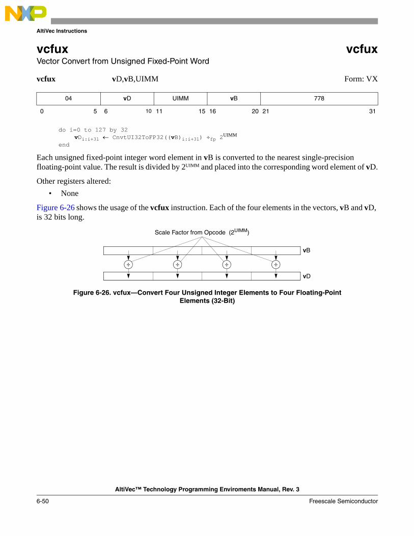
AltiVec Instructions
AltiVec™ Technology Programming Enviroments Manual, Rev. 3
6-50 Freescale Semiconductor
vcfux vcfuxVector Convert from Unsigned Fixed-Point Word
vcfux vD,vB,UIMM Form: VX
do i=0 to 127 by 32vDi:i+31 ← CnvtUI32ToFP32((vB)i:i+31) ÷fp 2
UIMM
end
Each unsigned fixed-point integer word element in vB is converted to the nearest single-precision floating-point value. The result is divided by 2UIMM and placed into the corresponding word element of vD.
Other registers altered: • None
Figure 6-26 shows the usage of the vcfux instruction. Each of the four elements in the vectors, vB and vD, is 32 bits long.
Figure 6-26. vcfux—Convert Four Unsigned Integer Elements to Four Floating-Point Elements (32-Bit)
04 vD UIMM vB 778
0 5 6 10 11 15 16 20 21 31
÷÷÷÷
Scale Factor from Opcode (2UIMM)
vB
vD

AltiVec Instructions
AltiVec™ Technology Programming Enviroments Manual, Rev. 3
Freescale Semiconductor 6-51
vcmpbfpx vcmpbfpxVector Compare Bounds Floating-Point
vcmpbfp vD,vA,vB (Rc=0) Form: VXRvcmpbfp. vD,vA,vB (Rc=1)
do i=0 to 127 by 32le ← ((vA)i:i+31 ≤fp (vB)i:i+31)ge ← ((vA)i:i+31 ≥fp -(vB)i:i+31)vDi:i+31 ← −le || −ge || 300
endif Rc=1 then do
ib ← (vD = 1280)CR24:27 ← 0b00 || ib || 0b0
end
Each single-precision word element in vA is compared to the corresponding element in vB. A 2-bit value is formed that indicates whether the element in vA is within the bounds specified by the element in vB, as follows.
Bit 0 of the 2-bit value is zero if the element in vA is less than or equal to the element in vB, and is one otherwise. Bit 1 of the 2-bit value is zero if the element in vA is greater than or equal to the negative of the element in vB, and is one otherwise.
The 2-bit value is placed into the high-order two bits of the corresponding word element (bits 0–1 for word element 0, bits 32–33 for word element 1, bits 64–65 for word element 2, bits 96–97 for word element 3) of vD and the remaining bits of the element are cleared.
If Rc=1, CR Field 6 is set to indicate whether all four elements in vA are within the bounds specified by the corresponding element in vB, as follows.
• CR6=0b00 || all_within_bounds || 0
Note that if any single-precision floating-point word element in vB is negative; the corresponding element in vA is out of bounds. Note that if a vA or a vB element is a NaN, the two high order bits of the corresponding result will both have the value 1.
If VSCR[NJ]=1, every denormalized operand element is truncated to 0 before the comparison is made.
Other registers altered:• Condition register (CR6):
Affected: Bit 2 (if Rc=1)
04 vD vA vB Rc 966
0 5 6 10 11 15 16 20 21 22 31
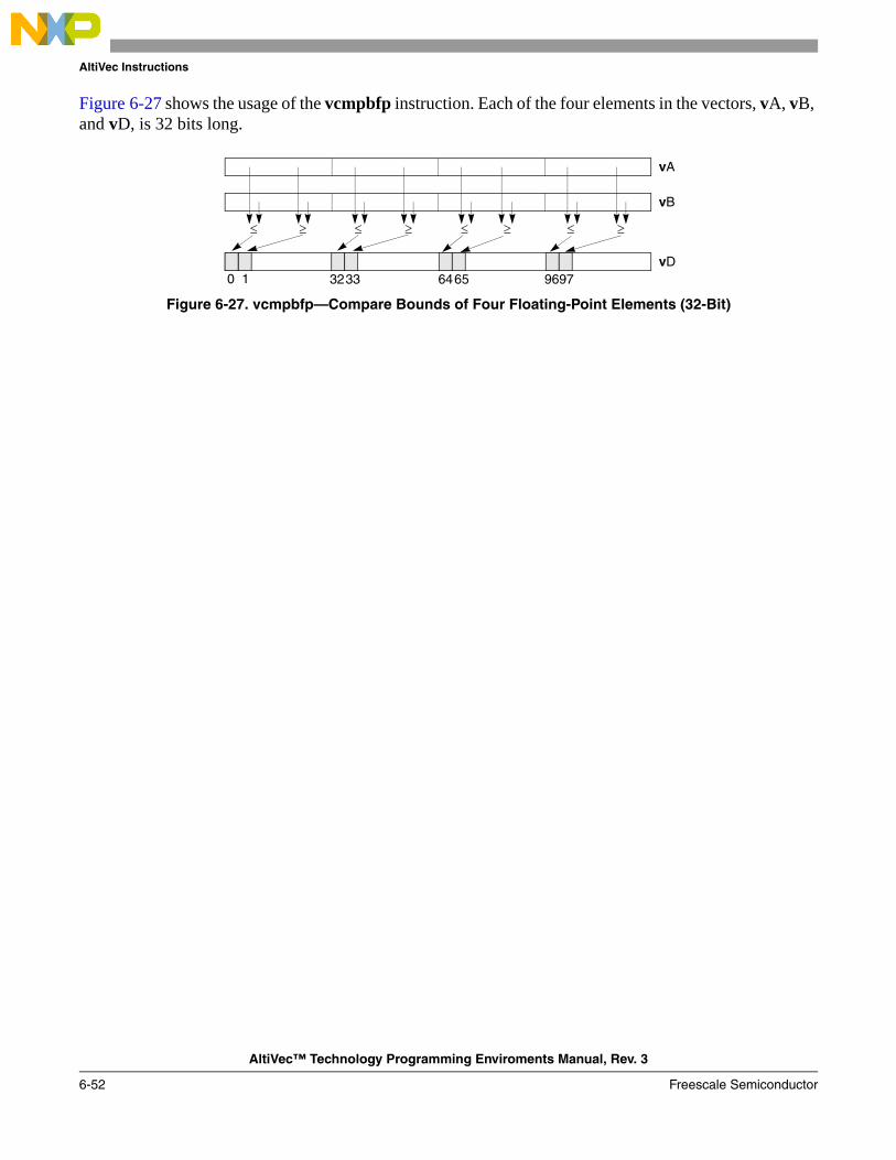
AltiVec Instructions
AltiVec™ Technology Programming Enviroments Manual, Rev. 3
6-52 Freescale Semiconductor
Figure 6-27 shows the usage of the vcmpbfp instruction. Each of the four elements in the vectors, vA, vB, and vD, is 32 bits long.
Figure 6-27. vcmpbfp—Compare Bounds of Four Floating-Point Elements (32-Bit)
≤
vA
vB
vD0 32 64 961 33
≥ ≤ ≥
65 97
≤ ≥ ≤ ≥

AltiVec Instructions
AltiVec™ Technology Programming Enviroments Manual, Rev. 3
Freescale Semiconductor 6-53
vcmpeqfpx vcmpeqfpxVector Compare Equal-to-Floating Point
vcmpeqfp vD,vA,vB Form: VXRvcmpeqfp. vD,vA,vB
do i=0 to 127 by 32
if (vA)i:i+31 =fp (vB)i:i+31then vDi:i+31 ← 0xFFFF_FFFFelse vDi:i+31 ← 0x0000_0000
end
if Rc=1 then dot ← (vD = 1281)f ← (vD = 1280)CR24:27 ← t || 0b0 || f || 0b0
end
Each single-precision floating-point word element in vA is compared to the corresponding single-precision floating-point word element in vB. The corresponding word element in vD is set to all 1s if the element in vA is equal to the element in vB, and is cleared to all 0s otherwise.
If Rc=1. CR6 filed is set according to all, some, or none of the elements pairs compare equal. • CR6=all_equal || 0b0 || none_equal || 0b0
Note that if a vA or vB element is a NaN, the corresponding result will be 0x0000_0000.
Other registers altered:• Condition register (CR6):
Affected: Bits 0–3 (if Rc=1)
Figure 6-28 shows the usage of the vcmpeqfp instruction. Each of the four elements in the vectors, vA, vB, and vD, is 32 bits long.
Figure 6-28. vcmpeqfp—Compare Equal of Four Floating-Point Elements (32-Bit)
04 vD vA vB Rc 198
0 5 6 10 11 15 16 20 21 22 31
====
vA
vB
vD

AltiVec Instructions
AltiVec™ Technology Programming Enviroments Manual, Rev. 3
6-54 Freescale Semiconductor
vcmpequbx vcmpequbxVector Compare Equal-to Unsigned Byte
vcmpequb vD,vA,vB Form: VXRvcmpequb. vD,vA,vB
do i=0 to 127 by 8
if (vA)i:i+7 =int (vB)i:i+7then vDi:i+7 ← 81else vDi:i+7 ← 80
end
if Rc=1 then do
t ← (vD = 1281)f ← (vD = 1280)CR[24:27] ← t || 0b0 || f || 0b0
end
Each element of vcmpequb is a byte.
Each integer element in vA is compared to the corresponding integer element in vB. The corresponding element in vD is set to all 1s if the element in vA is equal to the element in vB, and is cleared to all 0s otherwise.
The CR6 is set according to whether all, some, or none of the elements compare equal. • CR6=all_equal || 0b0 || none_equal || 0b0
Note that vcmpequb[.] can be used for unsigned or signed integers.
Other registers altered:• Condition register (CR6):
Affected: Bits 0–3 (if Rc=1)
Figure 6-29 shows the usage of the vcmpequb instruction. Each of the sixteen elements in the vectors, vA, vB, and vD, is 8 bits long.
Figure 6-29. vcmpequb—Compare Equal of Sixteen Integer Elements (8-Bit)
04 vD vA vB Rc 6
0 5 6 10 11 15 16 20 21 22 31
= = = = = = = = = = = = = == =
vA
vB
vD

AltiVec Instructions
AltiVec™ Technology Programming Enviroments Manual, Rev. 3
Freescale Semiconductor 6-55
vcmpequhx vcmpequhxVector Compare Equal-to Unsigned Half Word
vcmpequh vD,vA,vB Form: VXRvcmpequh. vD,vA,vB
do i=0 to 127 by 16
if (vA)i:i+15 =int (vB)i:i+15then vDi:i+15 ← 161else vDi:i+15 ← 160
end
if Rc=1 then do
t ← (vD = 1281)f ← (vD = 1280)CR[24:27] ← t || 0b0 || f || 0b0
end
Each element of vcmpequh is a half word.
Each integer element in vA is compared to the corresponding integer element in vB. The corresponding element in vD is set to all 1s if the element in vA is equal to the element in vB, and is cleared to all 0s otherwise.
The CR6 is set according to whether all, some, or none of the elements compare equal. • CR6=all_equal || 0b0 || none_equal || 0b0.
Note that vcmpequh[.] can be used for unsigned or signed integers.
Other registers altered:• Condition register (CR6):
Affected: Bits 0–3 (if Rc=1)
Figure 6-30 shows the usage of the vcmpequh instruction. Each of the eight elements in the vectors, vA, vB, and vD, is 16 bits long.
Figure 6-30. vcmpequh—Compare Equal of Eight Integer Elements (16-Bit)
04 vD vA vB Rc 70
0 5 6 10 11 15 16 20 21 22 31
= = ======
vA
vB
vD

AltiVec Instructions
AltiVec™ Technology Programming Enviroments Manual, Rev. 3
6-56 Freescale Semiconductor
vcmpequwx vcmpequwxVector Compare Equal-to Unsigned Word
vcmpequw vD,vA,vB Form: VXRvcmpequw. vD,vA,vB
do i=0 to 127 by 32
if (vA)i:i+311 =int (vB)i:i+31 then vDi:i+31 ← n1 else vDi:i+31 ← n0
end
if Rc=1 then dot ← (vD = 1281)f ← (vD = 1280)
CR[24:27] ← t || 0b0 || f || 0b0
end
Each element of vcmpequw is a word.
Each integer element in vA is compared to the corresponding integer element in vB. The corresponding element in vD is set to all 1s if the element in vA is equal to the element in vB, and is cleared to all 0s otherwise.
The CR6 is set according to whether all, some, or none of the elements compare equal. • CR6=all_equal || 0b0 || none_equal || 0b0
Note that vcmpequw[.] can be used for unsigned or signed integers.
Other registers altered:• Condition register (CR6):
Affected: Bits 0–3 (if Rc=1)
Figure 6-31 shows the usage of the vcmpequw instruction. Each of the four elements in the vectors, vA, vB, and vD, is 32 bits long.
Figure 6-31. vcmpequw—Compare Equal of Four Integer Elements (32-Bit)
04 vD vA vB Rc 134
0 5 6 10 11 15 16 20 21 22 31
= = = =
vA
vB
vD

AltiVec Instructions
AltiVec™ Technology Programming Enviroments Manual, Rev. 3
Freescale Semiconductor 6-57
vcmpgefpx vcmpgefpxVector Compare Greater-Than-or-Equal-to Floating-Point
vcmpgefp vD,vA,vB (Rc=0) Form: VXRvcmpgefp. vD,vA,vB (Rc=1)
do i=0 to 127 by 32if (vA)i:i+31 ≥fp (vB)i:i+31then vDi:i+31 ← 0xFFFF_FFFFelse vDi:i+31 ← 0x0000_0000
end
if Rc=1 then do
t ← (vD = 1281)f ← (vD = 1280)
CR24:27 ← t || 0b0 || f || 0b0
end
Each single-precision floating-point word element in vA is compared to the corresponding single-precision floating-point word element in vB. The corresponding word element in vD is set to all 1s if the element in vA is greater than or equal to the element in vB, and is cleared to all 0s otherwise.If Rc=1, CR6 is set according to all_greater_or_equal || some_greater_or_equal || none_great_or_equal.
CR6=all_greater_or_equal || 0b0 || none greater_or_equal || 0b0.
Note that if a vA or vB element is a NaN, the corresponding results will be 0x0000_0000.Other registers altered:
• Condition register (CR6):Affected: Bits 0–3 (if Rc=1)
Figure 6-32 shows the usage of the vcmpgefp instruction. Each of the four elements in the vectors, vA, vB, and vD, is 32 bits long
Figure 6-32. vcmpgefp—Compare Greater-Than-or-Equal of Four Floating-Point Elements (32-Bit)
04 vD vA vB Rc 454
0 5 6 10 11 15 16 20 21 22 31
≥≥≥≥
vA
vB
vD

AltiVec Instructions
AltiVec™ Technology Programming Enviroments Manual, Rev. 3
6-58 Freescale Semiconductor
vcmpgtfpx vcmpgtfpxVector Compare Greater-Than Floating-Point
vcmpgtfp vD,vA,vB Form: VXRvcmpgtfp. vD,vA,vB
do i=0 to 127 by 32if (vA)i:i+31 >fp (vB)i:i+31 then vDi:i+31 ← 0xFFFF_FFFF else vDi:i+31 ← 0x0000_0000
endif Rc=1 then do
t ← (vD = 1281)f ← (vD = 1280)CR[24:27] ← t || 0b0 || f || 0b0
end
Each single-precision floating-point word element in vA is compared to the corresponding single-precision floating-point word element in vB. The corresponding word element in vD is set to all 1s if the element in vA is greater than the element in vB, and is cleared to all 0s otherwise.
If Rc=1, CR6 is set according to all_greater_than || some_greater_than || none_greater_than.CR6=all_greater_than || 0b0 || none greater_than || 0b0.
Note that if a vA or vB element is a NaN, the corresponding results will be 0x0000_0000.
Other registers altered:• Condition register (CR6):
Affected: Bits 0–3 (if Rc=1)
Figure 6-33 shows the usage of the vcmpgtfp instruction. Each of the four elements in the vectors, vA, vB, and vD, is 32 bits long.
Figure 6-33. vcmpgtfp—Compare Greater-Than of Four Floating-Point Elements (32-Bit)
04 vD vA vB Rc 710
0 5 6 10 11 15 16 20 21 22 31
>>>>
vA
vB
vD
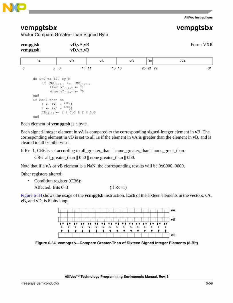
AltiVec Instructions
AltiVec™ Technology Programming Enviroments Manual, Rev. 3
Freescale Semiconductor 6-59
vcmpgtsbx vcmpgtsbxVector Compare Greater-Than Signed Byte
vcmpgtsb vD,vA,vB Form: VXRvcmpgtsb. vD,vA,vB
do i=0 to 127 by 8if (vA)i:i+7 >si (vB)i:i+7 then vDi:i+7 ← 81 else vDi:i+7 ← 80
endif Rc=1 then do
t ← (vD = 1281)f ← (vD = 1280)CR24:27 ← t || 0b0 || f || 0b0
end
Each element of vcmpgtsb is a byte.
Each signed-integer element in vA is compared to the corresponding signed-integer element in vB. The corresponding element in vD is set to all 1s if the element in vA is greater than the element in vB, and is cleared to all 0s otherwise.
If Rc=1, CR6 is set according to all_greater_than || some_greater_than || none_great_than.CR6=all_greater_than || 0b0 || none greater_than || 0b0.
Note that if a vA or vB element is a NaN, the corresponding results will be 0x0000_0000.
Other registers altered:• Condition register (CR6):
Affected: Bits 0–3 (if Rc=1)
Figure 6-34 shows the usage of the vcmpgtsb instruction. Each of the sixteen elements in the vectors, vA, vB, and vD, is 8 bits long.
Figure 6-34. vcmpgtsb—Compare Greater-Than of Sixteen Signed Integer Elements (8-Bit)
04 vD vA vB Rc 774
0 5 6 10 11 15 16 20 21 22 31
> >>>>>>>>>>>>>>>
vA
vB
vD

AltiVec Instructions
AltiVec™ Technology Programming Enviroments Manual, Rev. 3
6-60 Freescale Semiconductor
vcmpgtshx vcmpgtshxVector Compare Greater-Than Signed Half Word
vcmpgtsh vD,vA,vB Form: VXRvcmpgtsh. vD,vA,vB
do i=0 to 127 by 16
if (vA)i:i+15 >si (vB)i:i+15 then vDi:i+15 ← 161 else vDi:i+15 ← 160
endif Rc=1 then do
t ← (vD = 1281)f ← (vD = 1280)CR24:27 ← t || 0b0 || f || 0b0
end
Each element of vcmpgtsh is a half word.
Each signed-integer element in vA is compared to the corresponding signed-integer element in vB. The corresponding element in vD is set to all 1s if the element in vA is greater than the element in vB, and is cleared to all 0s otherwise.
If Rc=1, CR6 is set according to all_greater_than || some_greater_than || none_great_than.CR6=all_greater_than || 0b0 || none greater_than || 0b0.
Note that if a vA or vB element is a NaN, the corresponding results will be 0x0000_0000.
Other registers altered:• Condition register (CR6):
Affected: Bits 0–3 (if Rc=1)
Figure 6-35 shows the usage of the vcmpgtsh instruction. Each of the eight elements in the vectors, vA, vB, and vD, is 16 bits long.
Figure 6-35. vcmpgtsh—Compare Greater-Than of Eight Signed Integer Elements (16-Bit)
04 vD vA vB Rc 838
0 5 6 10 11 15 16 20 21 22 31
>>>>>>>>
vA
vB
vD
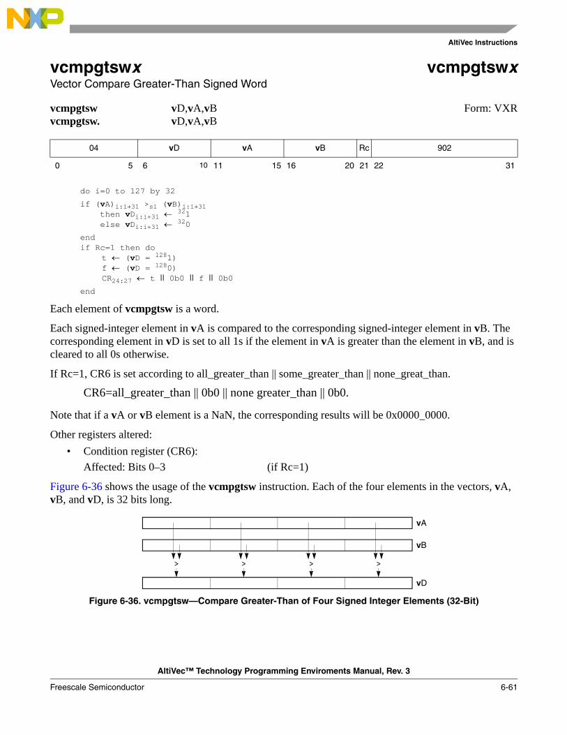
AltiVec Instructions
AltiVec™ Technology Programming Enviroments Manual, Rev. 3
Freescale Semiconductor 6-61
vcmpgtswx vcmpgtswxVector Compare Greater-Than Signed Word
vcmpgtsw vD,vA,vB Form: VXRvcmpgtsw. vD,vA,vB
do i=0 to 127 by 32
if (vA)i:i+31 >si (vB)i:i+31 then vDi:i+31 ← 321 else vDi:i+31 ← 320
endif Rc=1 then do
t ← (vD = 1281)f ← (vD = 1280)CR24:27 ← t || 0b0 || f || 0b0
end
Each element of vcmpgtsw is a word.
Each signed-integer element in vA is compared to the corresponding signed-integer element in vB. The corresponding element in vD is set to all 1s if the element in vA is greater than the element in vB, and is cleared to all 0s otherwise.
If Rc=1, CR6 is set according to all_greater_than || some_greater_than || none_great_than.
CR6=all_greater_than || 0b0 || none greater_than || 0b0.
Note that if a vA or vB element is a NaN, the corresponding results will be 0x0000_0000.
Other registers altered:• Condition register (CR6):
Affected: Bits 0–3 (if Rc=1)
Figure 6-36 shows the usage of the vcmpgtsw instruction. Each of the four elements in the vectors, vA, vB, and vD, is 32 bits long.
Figure 6-36. vcmpgtsw—Compare Greater-Than of Four Signed Integer Elements (32-Bit)
04 vD vA vB Rc 902
0 5 6 10 11 15 16 20 21 22 31
>>>>
vA
vB
vD
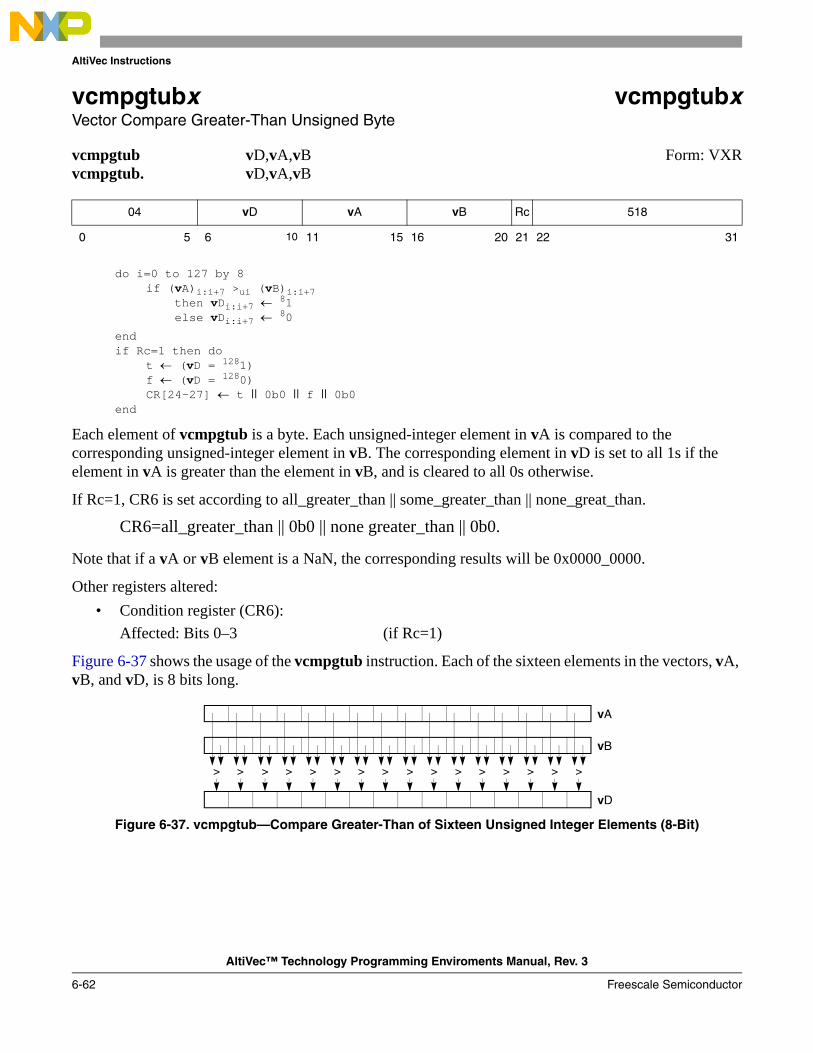
AltiVec Instructions
AltiVec™ Technology Programming Enviroments Manual, Rev. 3
6-62 Freescale Semiconductor
vcmpgtubx vcmpgtubxVector Compare Greater-Than Unsigned Byte
vcmpgtub vD,vA,vB Form: VXRvcmpgtub. vD,vA,vB
do i=0 to 127 by 8if (vA)i:i+7 >ui (vB)i:i+7 then vDi:i+7 ← 81 else vDi:i+7 ← 80
endif Rc=1 then do
t ← (vD = 1281)f ← (vD = 1280)CR[24–27] ← t || 0b0 || f || 0b0
end
Each element of vcmpgtub is a byte. Each unsigned-integer element in vA is compared to the corresponding unsigned-integer element in vB. The corresponding element in vD is set to all 1s if the element in vA is greater than the element in vB, and is cleared to all 0s otherwise.
If Rc=1, CR6 is set according to all_greater_than || some_greater_than || none_great_than.
CR6=all_greater_than || 0b0 || none greater_than || 0b0.
Note that if a vA or vB element is a NaN, the corresponding results will be 0x0000_0000.
Other registers altered:• Condition register (CR6):
Affected: Bits 0–3 (if Rc=1)
Figure 6-37 shows the usage of the vcmpgtub instruction. Each of the sixteen elements in the vectors, vA, vB, and vD, is 8 bits long.
Figure 6-37. vcmpgtub—Compare Greater-Than of Sixteen Unsigned Integer Elements (8-Bit)
04 vD vA vB Rc 518
0 5 6 10 11 15 16 20 21 22 31
> >>>>>>>>>>>>>>>
vA
vB
vD

AltiVec Instructions
AltiVec™ Technology Programming Enviroments Manual, Rev. 3
Freescale Semiconductor 6-63
vcmpgtuhx vcmpgtuhxVector Compare Greater-Than Unsigned Half Word
vcmpgtuh vD,vA,vB Form: VXRvcmpgtuh. vD,vA,vB
do i=0 to 127 by 16if (vA)i:i+151 >ui (vB)i:i+15 then vDi:i+15 ← 161 else vDi:i+15 ← 160
end
if Rc=1 then dot ← (vD = 1281)f ← (vD = 1280)CR[24–27] ← t || 0b0 || f || 0b0
end
Each element of vcmpgtuh is a half word. Each unsigned-integer element in vA is compared to the corresponding unsigned-integer element in vB. The corresponding element in vD is set to all 1s if the element in vA is greater than the element in vB, and is cleared to all 0s otherwise.
If Rc=1, CR6 is set according to all_greater_than || some_greater_than || none_great_than.
CR6=all_greater_than || 0b0 || none greater_than || 0b0.
Note that if a vA or vB element is a NaN, the corresponding results will be 0x0000_0000.
Other registers altered:• Condition register (CR6):
Affected: Bits 0–3 (if Rc=1)
Figure 6-38 shows the usage of the vcmpgtuh instruction. Each of the eight elements in the vectors, vA, vB, and vD, is 16 bits long.
Figure 6-38. vcmpgtuh—Compare Greater-Than of Eight Unsigned Integer Elements (16-Bit)
04 vD vA vB Rc 582
0 5 6 10 11 15 16 20 21 22 31
>>>>>>>>
vA
vB
vD

AltiVec Instructions
AltiVec™ Technology Programming Enviroments Manual, Rev. 3
6-64 Freescale Semiconductor
vcmpgtuwx vcmpgtuwxVector Compare Greater-Than Unsigned Word
vcmpgtuw vD,vA,vB Form: VXRvcmpgtuw. vD,vA,vB
do i=0 to 127 by 32if (vA)i:i+31 >ui (vB)i:i+31 then vDi:i+31 ← 321 else vDi:i+31 ← 320
end
if Rc=1 then do
t ← (vD = 1281)f ← (vD = 1280)CR[24–27] ← t || 0b0 || f || 0b0
end
Each element of vcmpgtuw is a word. Each unsigned-integer element in vA is compared to the corresponding unsigned-integer element in vB. The corresponding element in vD is set to all 1s if the element in vA is greater than the element in vB, and is cleared to all 0s otherwise.
If Rc=1, CR6 is set according to all_greater_than || some_greater_than || none_great_than.
CR6=all_greater_than || 0b0 || none_greater_than || 0b0.
Note that if a vA or vB element is a NaN, the corresponding results will be 0x0000_0000.
Other registers altered:• Condition register (CR6):
Affected: Bits 0–3 (if Rc=1)
Figure 6-39 shows the usage of the vcmpgtuw instruction. Each of the four elements in the vectors, vA, vB, and vD, is 32 bits long.
Figure 6-39. vcmpgtuw—Compare Greater-Than of Four Unsigned Integer Elements (32-Bit)
04 vD vA vB Rc 646
0 5 6 10 11 15 16 20 21 22 31
>>>>
vA
vB
vD
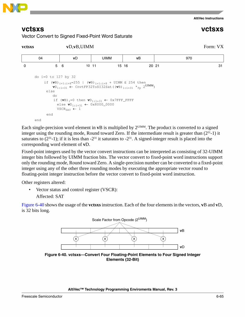
AltiVec Instructions
AltiVec™ Technology Programming Enviroments Manual, Rev. 3
Freescale Semiconductor 6-65
vctsxs vctsxsVector Convert to Signed Fixed-Point Word Saturate
vctsxs vD,vB,UIMM Form: VX
do i=0 to 127 by 32
if (vB)i+1:i+8=255 | (vB)i+1:i+8 + UIMM ≤ 254 then vDi:i+31 ← CnvtFP32ToSI32Sat((vB)i:i+31 *fp 2
UIMM) else do
if (vB)i=0 then vDi:i+31 ← 0x7FFF_FFFF else vDi:i+31 ← 0x8000_0000 VSCRSAT ← 1
end
end
Each single-precision word element in vB is multiplied by 2UIMM. The product is converted to a signed integer using the rounding mode, Round toward Zero. If the intermediate result is greater than (231-1) it saturates to (231-1); if it is less than -231 it saturates to -231. A signed-integer result is placed into the corresponding word element of vD.Fixed-point integers used by the vector convert instructions can be interpreted as consisting of 32-UIMM integer bits followed by UIMM fraction bits. The vector convert to fixed-point word instructions support only the rounding mode, Round toward Zero. A single-precision number can be converted to a fixed-point integer using any of the other three rounding modes by executing the appropriate vector round to floating-point integer instruction before the vector convert to fixed-point word instruction.
Other registers altered:• Vector status and control register (VSCR):
Affected: SAT
Figure 6-40 shows the usage of the vctsxs instruction. Each of the four elements in the vectors, vB and vD, is 32 bits long.
Figure 6-40. vctsxs—Convert Four Floating-Point Elements to Four Signed Integer Elements (32-Bit)
04 vD UIMM vB 970
0 5 6 10 11 15 16 20 21 31
vB
vD
xxxx
Scale Factor from Opcode (2UIMM)

AltiVec Instructions
AltiVec™ Technology Programming Enviroments Manual, Rev. 3
6-66 Freescale Semiconductor
vctuxs vctuxsVector Convert to Unsigned Fixed-Point Word Saturate
vctuxs vD,vB,UIMM Form: VX
do i=0 to 127 by 32if (vB)i+1:i+8=255 | (vB)i+1:i+8 + UIMM ≤ 254 then vDi:i+31 ← CnvtFP32ToUI32Sat((vB)i:i+31 *fp 2
UIM) else do if (vB)i=0 thenvDi:i+31 ← 0xFFFF_FFFF elsevDi:i+31 ← 0x0000_0000 VSCRSAT ← 1end
end
Each single-precision floating-point word element in vB is multiplied by 2UIM. The product is converted to an unsigned fixed-point integer using the rounding mode Round toward Zero.
If the intermediate result is greater than (232-1) it saturates to (232-1) and if it is less than 0 it saturates to 0.
The unsigned-integer result is placed into the corresponding word element of vD.
Other registers altered:• Vector status and control register (VSCR):
Affected: SAT
Figure 6-41 shows the usage of the vctuxs instruction. Each of the four elements in the vectors, vB and vD, is 32 bits long.
Figure 6-41. vctuxs—Convert Four Floating-Point Elements to Four Unsigned Integer Elements (32-Bit)
04 vD UIMM vB 906
0 5 6 10 11 15 16 20 21 31
vB
vD
xxxx
Scale Factor from Opcode (2UIMM)

AltiVec Instructions
AltiVec™ Technology Programming Enviroments Manual, Rev. 3
Freescale Semiconductor 6-67
vexptefp vexptefpVector 2 Raised to the Exponent Estimate Floating-Point
vexptefp vD,vB Form: VX
do i=0 to 127 by 32x ← (vB)i:i+31vDi:i+31 ← 2x
end
The single-precision floating-point estimate of 2 raised to the power of each single-precision floating-point element in vB is placed into the corresponding element of vD.
The estimate has a relative error in precision no greater than one part in 16, that is,
where x is the value of the element in vB. The most significant 12 bits of the estimate's significant are monotonic. Note that the value placed into the element of vD may vary between implementations, and between different executions on the same implementation.
If an operation has an integral value and the resulting value is not 0 or +∞, the result is exact.
Operation with various special values of the element in vB is summarized in Table 6-5 below.
If VSCR[NJ]=1, every denormalized operand element is truncated to a 0 of the same sign before the operation is carried out, and each denormalized result element truncates to a 0 of the same sign.
Other registers altered:• None
04 vD 0_0000 vB 394
0 5 6 10 11 15 16 20 21 31
Table 6-5. Special Values of the Element in vB
Value of Element in vB
Result
–∞ +0
–0 +1
+0 +1
+∞ +∞
NaN QNaN
estimate 2x–
2x
-------------------------------------116------≤

AltiVec Instructions
AltiVec™ Technology Programming Enviroments Manual, Rev. 3
6-68 Freescale Semiconductor
Figure 6-42 shows the usage of the vexptefp instruction. Each of the four elements in the vectors, vB and vD, is 32 bits long.
Figure 6-42. vexptefp—Two Raised to the Exponent Estimate Floating-Point for Four Floating-Point Elements (32-Bit)
2x2x2x
vB
vD
x x x x
2x

AltiVec Instructions
AltiVec™ Technology Programming Enviroments Manual, Rev. 3
Freescale Semiconductor 6-69
vlogefp vlogefpVector Log2 Estimate Floating-Point
vlogefp vD,vB Form: VX
do i=0 to 127 by 32x ← (vB)i:i+31vDi:i+31 ← log2(x)
end
The single-precision floating-point estimate of the base 2 logarithm of each single-precision floating-point element in vB is placed into the corresponding element of vD.
The estimate has an absolute error in precision (absolute value of the difference between the estimate and the infinitely precise value) no greater than 2-5. The estimate has a relative error in precision no greater than one part in 8, as described below:
where x is the value of the element in vB, except when |x-1| ≤ 1 ÷ 8. The most significant 12 bits of the estimate's significant are monotonic. Note that the value placed into the element of vD may vary between implementations, and between different executions on the same implementation.
Operation with various special values of the element in vB is summarized below in Table 6-6.
If VSCR[NJ]=1, every denormalized operand element is truncated to a 0 of the same sign before the operation is carried out, and each denormalized result element truncates to a 0 of the same sign.
Other registers altered:• None
04 vD 0_0000 vB 458
0 5 6 10 11 15 16 20 21 31
Table 6-6. Special Values of the Element in vB
Value Result
–∞ QNaN
less than 0 QNaN
±0 –∞
+∞ +∞
NaN QNaN
estimate - log2 x( ) 132------≤⎝ ⎠
⎛ ⎞ unless x 1– 18---≤

AltiVec Instructions
AltiVec™ Technology Programming Enviroments Manual, Rev. 3
6-70 Freescale Semiconductor
Figure 6-43 shows the usage of the vlogefp instruction. Each of the four elements in the vectors, vB and vD, is 32 bits long.
Figure 6-43. vlogefp—Log2 Estimate Floating-Point for Four Floating-Point Elements (32-Bit)
log2(x)log2(x)log2(x)log2(x)
vB
vD
x x x x

AltiVec Instructions
AltiVec™ Technology Programming Enviroments Manual, Rev. 3
Freescale Semiconductor 6-71
vmaddfp vmaddfpVector Multiply Add Floating-Point
vmaddfp vD,vA,vC,vB Form: VA
do i=0 to 127 by 32
vDi:i+31 ← RndToNearFP32(((vA)i:i+31 *fp (vC)i:i+31) +fp (vB)i:i+31)end
Each single-precision floating-point word element in vA is multiplied by the corresponding single-precision floating-point word element in vC. The corresponding single-precision floating-point word element in vB is added to the product. The result is rounded to the nearest single-precision floating-point number and placed into the corresponding word element of vD.
Note that a vector multiply floating-point instruction is not provided. The effect of such an instruction can be obtained by using vmaddfp with vB containing the value -0.0 (0x8000_0000) in each of its four single-precision floating-point word elements. (The value must be -0.0, not +0.0, in order to obtain the IEEE-conforming result of -0.0 when the result of the multiplication is -0.)
Other registers altered:• None
If VSCR[NJ]=1, every denormalized operand element is truncated to a 0 of the same sign before the operation is carried out, and each denormalized result element truncates to a 0 of the same sign. Figure 6-44 shows the usage of the vmaddfp instruction. Each of the four elements in the vectors, vA, vB, and vD, is 32 bits long.
Figure 6-44. vmaddfp—Multiply-Add Four Floating-Point Elements (32-Bit)
04 vD vA vB vC 46
0 5 6 10 11 15 16 20 21 26 31
+
Prod
vB
vD
* * * *
+ + +
vC
vA

AltiVec Instructions
AltiVec™ Technology Programming Enviroments Manual, Rev. 3
6-72 Freescale Semiconductor
vmaxfp vmaxfpVector Maximum Floating-Point
vmaxfp vD,vA,vB Form: VX
do i=0 to 127 by 32if (vA)i:i+31 ≥fp (vB)i:i+31 then vDi:i+31 ← (vA)i:i+31 else vDi:i+31 ← (vB)i:i+31
end
Each single-precision floating-point word element in vA is compared to the corresponding single-precision floating-point word element in vB. The larger of the two single-precision floating-point values is placed into the corresponding word element of vD.
The maximum of +0 and -0 is +0. The maximum of any value and a NaN is a QNaN.
Other registers altered:• None
Figure 6-45 shows the usage of the vmaxfp instruction. Each of the four elements in the vectors, vA, vB, and vD, is 32 bits long.
Figure 6-45. vmaxfp—Maximum of Four Floating-Point Elements (32-Bit)
04 vD vA vB 1034
0 5 6 10 11 15 16 20 21 31
≥fp≥fp≥fp≥fp
vA
vB
vD

AltiVec Instructions
AltiVec™ Technology Programming Enviroments Manual, Rev. 3
Freescale Semiconductor 6-73
vmaxsb vmaxsbVector Maximum Signed Byte
vmaxsb vD,vA,vB Form: VX
do i=0 to 127 by 8if (vA)i:i+7 ≥si (vB)i:i+7 then vDi:i+7 ← (vA)i:i+7 else vDi:i+7 ← (vB)i:i+7
end
Each element of vmaxsb is a byte.
Each signed-integer element in vA is compared to the corresponding signed-integer element in vB. The larger of the two signed-integer values is placed into the corresponding element of vD.
Other registers altered:• None
Figure 6-46 shows the usage of the vmaxsb instruction. Each of the sixteen elements in the vectors, vA, vB, and vD, is 8 bits long.
Figure 6-46. vmaxsb—Maximum of Sixteen Signed Integer Elements (8-Bit)
04 vD vA vB 258
0 5 6 10 11 15 16 20 21 31
≥si ≥si≥si≥si≥si≥si≥si≥si≥si≥si≥si≥si≥si≥si≥si≥si
vA
vB
vD

AltiVec Instructions
AltiVec™ Technology Programming Enviroments Manual, Rev. 3
6-74 Freescale Semiconductor
vmaxsh vmaxshVector Maximum Signed Half Word
vmaxsh vD,vA,vB Form: VX
do i=0 to 127 by 16if (vA)i:i+7 ≥si (vB)i:i+15 then vDi:i+15 ← (vA)i:i+15 else vDi:i+15 ← (vB)i:i+15
end
Each element of vmaxsh is a half word.
Each signed-integer element in vA is compared to the corresponding signed-integer element in vB. The larger of the two signed-integer values is placed into the corresponding element of vD.
Other registers altered:• None
Figure 6-47 shows the usage of the vmaxsh instruction. Each of the eight elements in the vectors, vA, vB, and vD, is 16 bits long.
Figure 6-47. vmaxsh—Maximum of Eight Signed Integer Elements (16-Bit)
04 vD vA vB 322
0 5 6 10 11 15 16 20 21 31
≥si≥si≥si≥si≥si≥si≥si≥si
vA
vB
vD
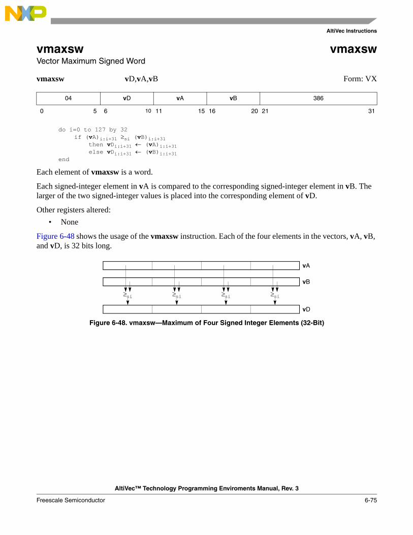
AltiVec Instructions
AltiVec™ Technology Programming Enviroments Manual, Rev. 3
Freescale Semiconductor 6-75
vmaxsw vmaxswVector Maximum Signed Word
vmaxsw vD,vA,vB Form: VX
do i=0 to 127 by 32if (vA)i:i+31 ≥si (vB)i:i+31 then vDi:i+31 ← (vA)i:i+31 else vDi:i+31 ← (vB)i:i+31
end
Each element of vmaxsw is a word.
Each signed-integer element in vA is compared to the corresponding signed-integer element in vB. The larger of the two signed-integer values is placed into the corresponding element of vD.
Other registers altered:• None
Figure 6-48 shows the usage of the vmaxsw instruction. Each of the four elements in the vectors, vA, vB, and vD, is 32 bits long.
Figure 6-48. vmaxsw—Maximum of Four Signed Integer Elements (32-Bit)
04 vD vA vB 386
0 5 6 10 11 15 16 20 21 31
≥si≥si≥si≥si
vA
vB
vD

AltiVec Instructions
AltiVec™ Technology Programming Enviroments Manual, Rev. 3
6-76 Freescale Semiconductor
vmaxub vmaxubVector Maximum Unsigned Byte
vmaxub vD,vA,vB Form: VX
do i=0 to 127 by 8if (vA)i:i+7 ≥ui (vB)i:i+7 then vDi:i+7 ← (vA)i:i+7 else vDi:i+7 ← (vB)i:i+7
end
Each element of vmaxub is a byte.
Each unsigned-integer element in vA is compared to the corresponding unsigned-integer element in vB. The larger of the two unsigned-integer values is placed into the corresponding element of vD.
Other registers altered:• None
Figure 6-49 shows the usage of the vmaxub instruction. Each of the sixteen elements in the vectors, vA, vB, and vD, is 8 bits long.
Figure 6-49. vmaxub—Maximum of Sixteen Unsigned Integer Elements (8-Bit)
04 vD vA vB 2
0 5 6 10 11 15 16 20 21 31
≥ui ≥ui≥ui≥ui≥ui≥ui≥ui≥ui≥ui≥ui≥ui≥ui≥ui≥ui≥ui≥ui
vA
vB
vD

AltiVec Instructions
AltiVec™ Technology Programming Enviroments Manual, Rev. 3
Freescale Semiconductor 6-77
vmaxuh vmaxuhVector Maximum Unsigned Half Word
vmaxuh vD,vA,vB Form: VX
do i=0 to 127 by 16if (vA)i:i+15 ≥ui (vB)i:i+15 then vDi:i+15 ← (vA)i:i+15 else vDi:i+15 ← (vB)i:i+15
end
Each element of vmaxuh is a half word.
Each unsigned-integer element in vA is compared to the corresponding unsigned-integer element in vB. The larger of the two unsigned-integer values is placed into the corresponding element of vD.
Other registers altered:• None
Figure 6-50 shows the usage of the vmaxuh instruction. Each of the eight elements in the vectors, vA, vB, and vD, is 16 bits long.
Figure 6-50. vmaxuh—Maximum of Eight Unsigned Integer Elements (16-Bit)
04 vD vA vB 66
0 5 6 10 11 15 16 20 21 31
≥ui≥ui≥ui≥ui≥ui≥ui≥ui≥ui
vA
vB
vD

AltiVec Instructions
AltiVec™ Technology Programming Enviroments Manual, Rev. 3
6-78 Freescale Semiconductor
vmaxuw vmaxuwVector Maximum Unsigned Word
vmaxuw vD,vA,vB Form: VX
do i=0 to 127 by 32if (vA)i:i+31 ≥ui (vB)i:i+31 then vDi:i+31 ← (vA)i:i+31 else vDi:i+31 ← (vB)i:i+31
end
Each element of vmaxuw is a word.
Each unsigned-integer element in vA is compared to the corresponding unsigned-integer element in vB. The larger of the two unsigned-integer values is placed into the corresponding element of vD.
Other registers altered:• None
Figure 6-51 shows the usage of the vmaxuw instruction. Each of the four elements in the vectors, vA, vB, and vD, is 32 bits long.
Figure 6-51. vmaxuw—Maximum of Four Unsigned Integer Elements (32-Bit)
04 vD vA vB 130
0 5 6 10 11 15 16 20 21 31
≥ui≥ui≥ui≥ui
vA
vB
vD

AltiVec Instructions
AltiVec™ Technology Programming Enviroments Manual, Rev. 3
Freescale Semiconductor 6-79
vmhaddshs vmhaddshsVector Multiply High and Add Signed Half Word Saturate
vmhaddshs vD,vA,vB,vC Form: VA
do i=0 to 127 by 16
prod0:31 ← (vA)i:i+15 *si (vB)i:i+15 temp0:16 ← prod0:16 +int SignExtend((vC)i:i+15,17) vDi:i+15 ← SItoSIsat(temp0:16,16)
end
Each signed-integer half-word element in vA is multiplied by the corresponding signed-integer half-word element in vB, producing a 32-bit signed-integer product. Bits 0–16 of the intermediate product are added to the corresponding signed-integer half-word element in vC after they have been sign extended to 17 bits. The 16-bit saturated result from each of the eight 17-bit sums is placed in register vD.
If the intermediate result is greater than (215-1) it saturates to (215-1) and if it is less than (-215) it saturates to (-215).The signed-integer result is placed into the corresponding half-word element of vD.Other registers altered:
• Vector status and control register (VSCR):Affected: SAT
Figure 6-52 shows the usage of the vmhaddshs instruction. Each of the eight elements in the vectors, vA, vB, vC, and vD, is 16 bits long.
Figure 6-52. vmhaddshs—Multiply-High and Add Eight Signed Integer Elements (16-Bit)
04 vD vA vB vC 32
0 5 6 10 11 15 16 20 21 25 26 31
+
S
vA
vB
Prod
vC
Temp
vD
* * * * * * * *
+
S
Sat
1716
16+
S
+
S
+
S
+
S
+
S
+
S
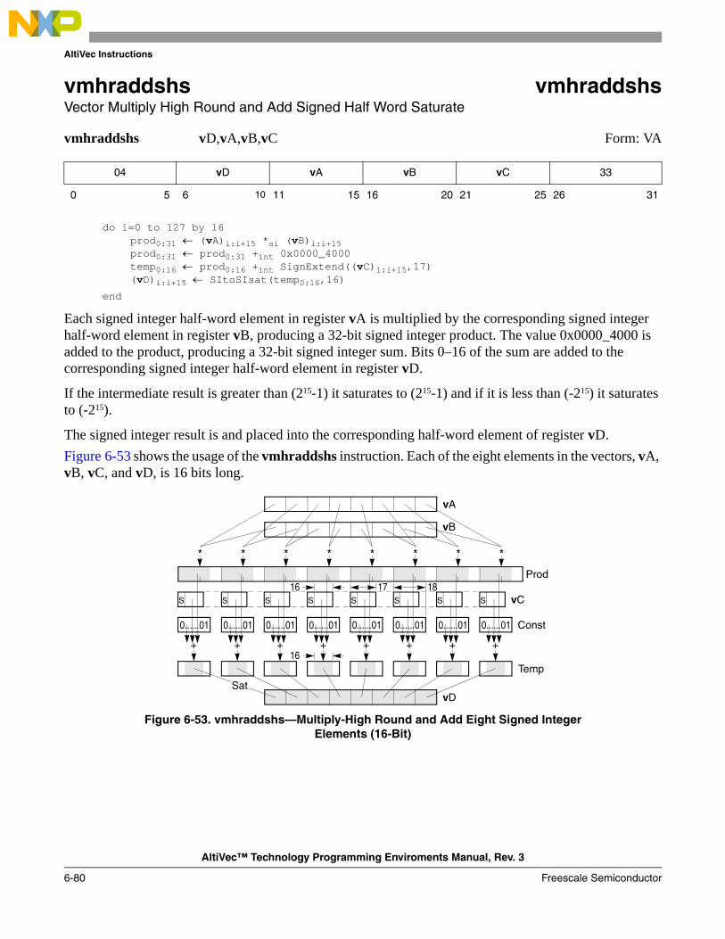
AltiVec Instructions
AltiVec™ Technology Programming Enviroments Manual, Rev. 3
6-80 Freescale Semiconductor
vmhraddshs vmhraddshsVector Multiply High Round and Add Signed Half Word Saturate
vmhraddshs vD,vA,vB,vC Form: VA
do i=0 to 127 by 16prod0:31 ← (vA)i:i+15 *si (vB)i:i+15prod0:31 ← prod0:31 +int 0x0000_4000temp0:16 ← prod0:16 +int SignExtend((vC)i:i+15,17) (vD)i:i+15 ← SItoSIsat(temp0:16,16)
end
Each signed integer half-word element in register vA is multiplied by the corresponding signed integer half-word element in register vB, producing a 32-bit signed integer product. The value 0x0000_4000 is added to the product, producing a 32-bit signed integer sum. Bits 0–16 of the sum are added to the corresponding signed integer half-word element in register vD.
If the intermediate result is greater than (215-1) it saturates to (215-1) and if it is less than (-215) it saturates to (-215).
The signed integer result is and placed into the corresponding half-word element of register vD.Figure 6-53 shows the usage of the vmhraddshs instruction. Each of the eight elements in the vectors, vA, vB, vC, and vD, is 16 bits long.
Figure 6-53. vmhraddshs—Multiply-High Round and Add Eight Signed Integer Elements (16-Bit)
04 vD vA vB vC 33
0 5 6 10 11 15 16 20 21 25 26 31
+
vA
vB
Prod
Const
Temp
vD
* * * * * * * *
+
Sat
1716
16+ + ++++
0......01
S vCS S S SSSS
18
0......01 0......01 0......01 0......01 0......01 0......01 0......01

AltiVec Instructions
AltiVec™ Technology Programming Enviroments Manual, Rev. 3
Freescale Semiconductor 6-81
vminfp vminfpVector Minimum Floating-Point
vminfp vD,vA,vB Form: VX
do i=0 to 127 by 32if (vA)i:i+31 <fp (vB)i:i+31 then vDi:i+31 ← (vA)i:i+31 else vDi:i+31 ← (vB)i:i+31
end
Each single-precision floating-point word element in register vA is compared to the corresponding single-precision floating-point word element in register vB. The smaller of the two single-precision floating-point values is placed into the corresponding word element of register vD.
The minimum of +0.0 and -0.0 is -0.0. The minimum of any value and a NaN is a QNaN.
If VSCR[NJ]=1, every denormalized operand element is truncated to 0 before the comparison is made.
Figure 6-54 shows the usage of the vminfp instruction. Each of the four elements in the vectors, vA, vB, and vD, is 32 bits long.
Figure 6-54. vminfp—Minimum of Four Floating-Point Elements (32-Bit)
04 vD vA vB 1098
0 5 6 10 11 15 16 20 21 31
<fp<fp<fp<fp
vA
vB
vD

AltiVec Instructions
AltiVec™ Technology Programming Enviroments Manual, Rev. 3
6-82 Freescale Semiconductor
vminsb vminsbVector Minimum Signed Byte
vminsb vD,vA,vB Form: VX
do i=0 to 127 by 8if (vA)i:i+7 <si (vB)i:i+7 then vDi:i+7 ← (vA)i:i+7 else vDi:i+7 ← (vB)i:i+7
end
Each element of vminsb is a byte.
Each signed-integer element in vA is compared to the corresponding signed-integer element in vB. The larger of the two signed-integer values is placed into the corresponding element of vD.
Other registers altered:• None
Figure 6-55 shows the usage of the vminsb instruction. Each of the sixteen elements in the vectors, vA, vB, and vD, is 8 bits long.
Figure 6-55. vminsb—Minimum of Sixteen Signed Integer Elements (8-Bit)
04 vD vA vB 770
0 5 6 10 11 15 16 20 21 31
<si <si<si<si<si<si<si<si<si<si<si<si<si<si<si<si
vA
vB
vD

AltiVec Instructions
AltiVec™ Technology Programming Enviroments Manual, Rev. 3
Freescale Semiconductor 6-83
vminsh vminshVector Minimum Signed Half Word
vminsh vD,vA,vB Form: VX
do i=0 to 127 by 16if (vA)i:i+15<si (vB)i:i+15 then vDi:i+15 ← (vA)i:i+15 else vDi:i+15 ← (vB)i:i+15
end
Each element of vminsh is a half word.
Each signed-integer element in vA is compared to the corresponding signed-integer element in vB. The larger of the two signed-integer values is placed into the corresponding element of vD.
Other registers altered:• None
Figure 6-56 shows the usage of the vminsh instruction. Each of the eight elements in the vectors, vA, vB, and vD, is 16 bits long.
Figure 6-56. vminsh—Minimum of Eight Signed Integer Elements (16-Bit)
04 vD vA vB 834
0 5 6 10 11 15 16 20 21 31
<si<si<si<si<si<si<si<si
vA
vB
vD
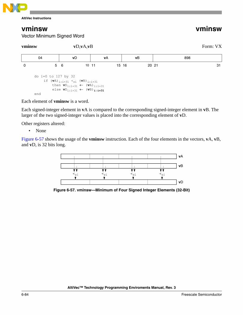
AltiVec Instructions
AltiVec™ Technology Programming Enviroments Manual, Rev. 3
6-84 Freescale Semiconductor
vminsw vminswVector Minimum Signed Word
vminsw vD,vA,vB Form: VX
do i=0 to 127 by 32if (vA)i:i+31 <si (vB)i:i+31 then vDi:i+31 ← (vA)i:i+31 else vDi:i+31 ← (vB)i:i+31
end
Each element of vminsw is a word.
Each signed-integer element in vA is compared to the corresponding signed-integer element in vB. The larger of the two signed-integer values is placed into the corresponding element of vD.
Other registers altered:• None
Figure 6-57 shows the usage of the vminsw instruction. Each of the four elements in the vectors, vA, vB, and vD, is 32 bits long.
Figure 6-57. vminsw—Minimum of Four Signed Integer Elements (32-Bit)
04 vD vA vB 898
0 5 6 10 11 15 16 20 21 31
<si<si<si<si
vA
vB
vD
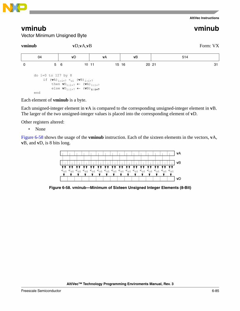
AltiVec Instructions
AltiVec™ Technology Programming Enviroments Manual, Rev. 3
Freescale Semiconductor 6-85
vminub vminubVector Minimum Unsigned Byte
vminub vD,vA,vB Form: VX
do i=0 to 127 by 8if (vA)i:i+7 <ui (vB)i:i+7 then vDi:i+7 ← (vA)i:i+7 else vDi:i+7 ← (vB)i:i+7
end
Each element of vminub is a byte.
Each unsigned-integer element in vA is compared to the corresponding unsigned-integer element in vB. The larger of the two unsigned-integer values is placed into the corresponding element of vD.
Other registers altered:• None
Figure 6-58 shows the usage of the vminub instruction. Each of the sixteen elements in the vectors, vA, vB, and vD, is 8 bits long.
Figure 6-58. vminub—Minimum of Sixteen Unsigned Integer Elements (8-Bit)
04 vD vA vB 514
0 5 6 10 11 15 16 20 21 31
<ui <ui<ui<ui<ui<ui<ui<ui<ui<ui<ui<ui<ui<ui<ui<ui
vA
vB
vD

AltiVec Instructions
AltiVec™ Technology Programming Enviroments Manual, Rev. 3
6-86 Freescale Semiconductor
vminuh vminuhVector Minimum Unsigned Half Word
vminuh vD,vA,vB Form: VX
do i=0 to 127 by 16if (vA)i:i+15 <ui (vB)i:i+15 then vDi:i+15 ← (vA)i:i+15 else vDi:i+15 ← (vB)i:i+15
end
Each element of vminuh is a half word.
Each unsigned-integer element in vA is compared to the corresponding unsigned-integer element in vB. The larger of the two unsigned-integer values is placed into the corresponding element of vD.
Other registers altered:• None
Figure 6-59 shows the usage of the vminuh instruction. Each of the eight elements in the vectors, vA, vB, and vD, is 16 bits long.
Figure 6-59. vminuh—Minimum of Eight Unsigned Integer Elements (16-Bit)
04 vD vA vB 578
0 5 6 10 11 15 16 20 21 31
<ui<ui<ui<ui<ui<ui<ui<ui
vA
vB
vD
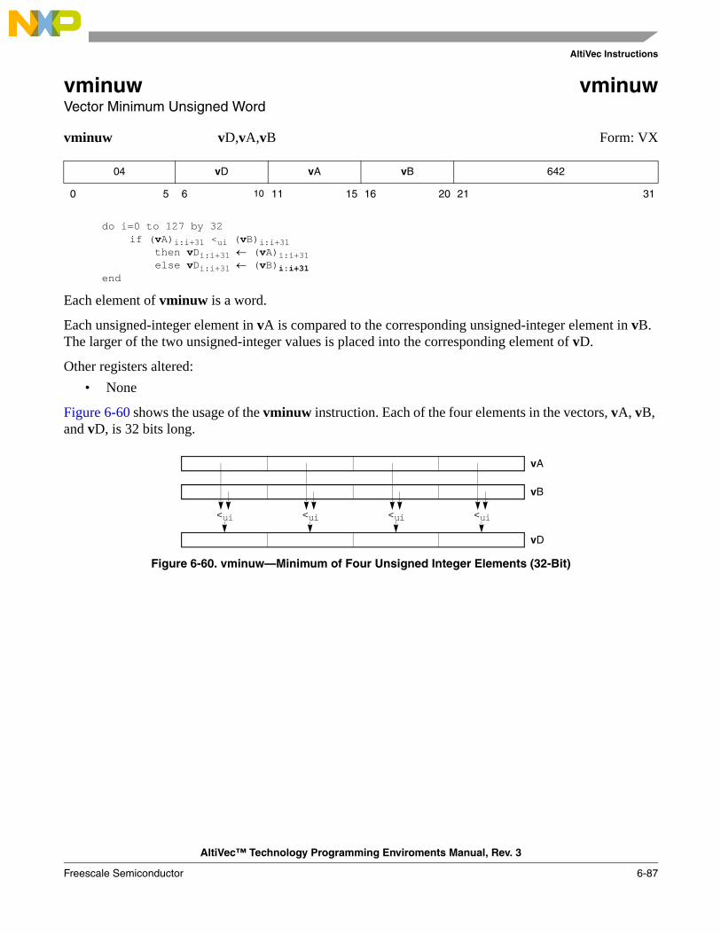
AltiVec Instructions
AltiVec™ Technology Programming Enviroments Manual, Rev. 3
Freescale Semiconductor 6-87
vminuw vminuwVector Minimum Unsigned Word
vminuw vD,vA,vB Form: VX
do i=0 to 127 by 32if (vA)i:i+31 <ui (vB)i:i+31 then vDi:i+31 ← (vA)i:i+31 else vDi:i+31 ← (vB)i:i+31
end
Each element of vminuw is a word.
Each unsigned-integer element in vA is compared to the corresponding unsigned-integer element in vB. The larger of the two unsigned-integer values is placed into the corresponding element of vD.
Other registers altered:• None
Figure 6-60 shows the usage of the vminuw instruction. Each of the four elements in the vectors, vA, vB, and vD, is 32 bits long.
Figure 6-60. vminuw—Minimum of Four Unsigned Integer Elements (32-Bit)
04 vD vA vB 642
0 5 6 10 11 15 16 20 21 31
<ui<ui<ui<ui
vA
vB
vD

AltiVec Instructions
AltiVec™ Technology Programming Enviroments Manual, Rev. 3
6-88 Freescale Semiconductor
vmladduhm vmladduhmVector Multiply Low and Add Unsigned Half Word Modulo
vmladduhm vD,vA,vB,vC Form: VA
do i=0 to 127 by 16prod0:31 ← (vA)i:i+15 *ui (vB)i:i+15vDi:i+15 ← prod0:31 +int (vC)i:i+15
end
Each integer half-word element in vA is multiplied by the corresponding integer half-word element in vB, producing a 32-bit integer product. The product is added to the corresponding integer half-word element in vC. The integer result is placed into the corresponding half-word element of vD.
Note that vmladduhm can be used for unsigned or signed integers.
Other registers altered: • None
Figure 6-61 shows the usage of the vmladduhm instruction. Each of the eight elements in the vectors, vA, vB, vC, and vD, is 16 bits long.
Figure 6-61. vmladduhm—Multiply-Add of Eight Integer Elements (16-Bit)
04 vD vA vB vC 34
0 5 6 10 11 15 16 20 21 25 26 31
+
vA
vB
Prod
vC
Temp
vD
* * * * * * * *
+ + + ++++

AltiVec Instructions
AltiVec™ Technology Programming Enviroments Manual, Rev. 3
Freescale Semiconductor 6-89
vmrghb vmrghbVector Merge High Byte
vmrghb vD,vA,vB Form: VX
do i=0 to 63 by 8vDi*2:(i*2)+15 ← (vA)i:i+7 || (vB)i:i+7
end
Each element of vmrghb is a byte.
The elements in the high-order half of vA are placed, in the same order, into the even-numbered elements of vD. The elements in the high-order half of vB are placed, in the same order, into the odd-numbered elements of vD.
Other registers altered:• None
Figure 6-62 shows the usage of the vmrghb instruction. Each of the sixteen elements in the vectors, vA, vB, and vD, is 8 bits long.
Figure 6-62. vmrghb—Merge Eight High-Order Elements (8-Bit)
04 vD vA vB 12
0 5 6 10 11 15 16 20 21 31
vA
vB
vD

AltiVec Instructions
AltiVec™ Technology Programming Enviroments Manual, Rev. 3
6-90 Freescale Semiconductor
vmrghh vmrghhVector Merge High Half word
vmrghh vD,vA,vB Form: VX
do i=0 to 63 by 16vDi*2:(i*2)+31 ← (vA)i:i+15 || (vB)i:i+15
end
Each element of vmrghh is a half word.
The elements in the high-order half of vA are placed, in the same order, into the even-numbered elements of vD. The elements in the high-order half of vB are placed, in the same order, into the odd-numbered elements of vD.
Other registers altered:• None
Figure 6-63 shows the usage of the vmrghh instruction. Each of the eight elements in the vectors, vA, vB, and vD, is 16 bits long.
Figure 6-63. vmrghh—Merge Four High-Order Elements (16-Bit)
04 vD vA vB 76
0 5 6 10 11 15 16 20 21 31
vA
vB
vD
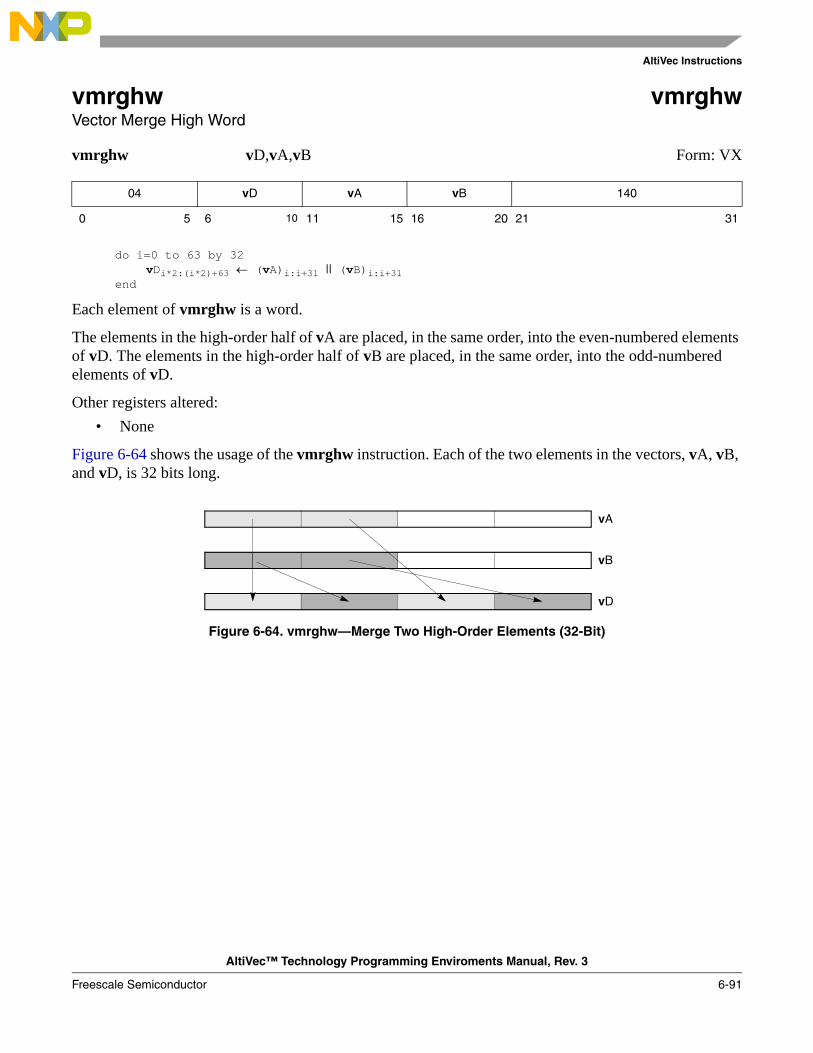
AltiVec Instructions
AltiVec™ Technology Programming Enviroments Manual, Rev. 3
Freescale Semiconductor 6-91
vmrghw vmrghwVector Merge High Word
vmrghw vD,vA,vB Form: VX
do i=0 to 63 by 32vDi*2:(i*2)+63 ← (vA)i:i+31 || (vB)i:i+31
end
Each element of vmrghw is a word.
The elements in the high-order half of vA are placed, in the same order, into the even-numbered elements of vD. The elements in the high-order half of vB are placed, in the same order, into the odd-numbered elements of vD.
Other registers altered:• None
Figure 6-64 shows the usage of the vmrghw instruction. Each of the two elements in the vectors, vA, vB, and vD, is 32 bits long.
Figure 6-64. vmrghw—Merge Two High-Order Elements (32-Bit)
04 vD vA vB 140
0 5 6 10 11 15 16 20 21 31
vA
vB
vD

AltiVec Instructions
AltiVec™ Technology Programming Enviroments Manual, Rev. 3
6-92 Freescale Semiconductor
vmrglb vmrglbVector Merge Low Byte
vmrglb vD,vA,vB Form: VX
do i=0 to 63 by 8vDi*2:(i*2)+15 ← (vA)i+64:i+71 || (vB)i+64:i+71
end
Each element offer vmrglb is a byte.
The elements in the low-order half of vA are placed, in the same order, into the even-numbered elements of vD. The elements in the low-order half of vB are placed, in the same order, into the odd-numbered elements of vD.
Other registers altered:• None
Figure 6-65 shows the usage of the vmrglb instruction. Each of the sixteen elements in the vectors, vA, vB, and vD, is 8 bits long.
Figure 6-65. vmrglb—Merge Eight Low-Order Elements (8-Bit)
04 vD vA vB 268
0 5 6 10 11 15 16 20 21 31
vA
vB
vD

AltiVec Instructions
AltiVec™ Technology Programming Enviroments Manual, Rev. 3
Freescale Semiconductor 6-93
vmrglh vmrglhVector Merge Low Half Word
vmrglh vD,vA,vB Form: VX
do i=0 to 63 by 16vDi*2:(i*2)+31 ← (vA)i+64:i+79 || (vB)i+64:i+79
end
Each element of vmrglh is a half word.
The elements in the low-order half of vA are placed, in the same order, into the even-numbered elements of vD. The elements in the low-order half of vB are placed, in the same order, into the odd-numbered elements of vD.
Other registers altered:• None
Figure 6-66 shows the usage of the vmrglh instruction. Each of the eight elements in the vectors, vA, vB, and vD, is 16 bits long.
Figure 6-66. vmrglh—Merge Four Low-Order Elements (16-Bit)
04 vD vA vB 332
0 5 6 10 11 15 16 20 21 31
vA
vB
vD

AltiVec Instructions
AltiVec™ Technology Programming Enviroments Manual, Rev. 3
6-94 Freescale Semiconductor
vmrglw vmrglwVector Merge Low Word
vmrglw vD,vA,vB Form: VX
do i=0 to 63 by 32vDi*2:(i*2)+63 ← (vA)i+64:i+95 || (vB)i+64:i+95
end
Each element of vmrglw is a word.
The elements in the low-order half of vA are placed, in the same order, into the even-numbered elements of vD. The elements in the low-order half of vB are placed, in the same order, into the odd-numbered elements of vD.
Other registers altered:• None
Figure 6-67 shows the usage of the vmrglw instruction. Each of the four elements in the vectors, vA, vB, and vD, is 32 bits long.
Figure 6-67. vmrglw—Merge Four Low-Order Elements (32-Bit)
04 vD vA vB 396
0 5 6 10 11 15 16 20 21 31
vA
vB
vD

AltiVec Instructions
AltiVec™ Technology Programming Enviroments Manual, Rev. 3
Freescale Semiconductor 6-95
vmsummbm vmsummbmVector Multiply Sum Mixed-Sign Byte Modulo
vmsummbm vD,vA,vB,vC Form: VA
do i=0 to 127 by 32temp0:31 ← (vC)i:i+31 do j=0 to 31 by 8
prod0:15 ← (vA)i+j:i+j+7 *sui (vB)i+j:i+j+7temp0:31 ← temp0:31 +int SignExtend(prod0:15,32)end
vDi:i+31 ← temp0:31end
For each word element in vC the following operations are performed in the order shown.• Each of the four signed-integer byte elements contained in the corresponding word element of vA
is multiplied by the corresponding unsigned-integer byte element in vB, producing a signed-integer 16-bit product.
• The signed-integer modulo sum of these four products is added to the signed-integer word element in vC.
• The signed-integer result is placed into the corresponding word element of vD.
Other registers altered:• None
Figure 6-68 shows the usage of the vmsummbm instruction. Each of the sixteen elements in the vectors, vA and vB, are 8 bits long. Each of the four elements in the vectors, vC and vD, are 32 bits long.
Figure 6-68. vmsummbm—Multiply-Sum of Integer Elements (8- to 32-Bit)
04 vD vA vB vC 37
0 5 6 10 11 15 16 20 21 25 26 31
vA
vB
Prod
vD
* * * * * * * * * * * * * * * *
+ + + +
vC

AltiVec Instructions
AltiVec™ Technology Programming Enviroments Manual, Rev. 3
6-96 Freescale Semiconductor
vmsumshm vmsumshmVector Multiply Sum Signed Half Word Modulo
vmsumshm vD,vA,vB,vC Form: VA
do i=0 to 127 by 32
temp0:31 ← (vC)i:i+31 do j=0 to 31 by 16
prod0:31 ← (vA)i+j:i+j+15 *si (vB)i+j:i+j+15temp0:31 ← temp0:31 +int prod0:31vDi:i+31 ← temp0:31
end
end
For each word element in vC the following operations are performed in the order shown.• Each of the two signed-integer half-word elements contained in the corresponding word element
of vA is multiplied by the corresponding signed-integer half-word element in vB, producing a signed-integer 32-bit product.
• The signed-integer modulo sum of these two products is added to the signed-integer word element in vC.
• The signed-integer result is placed into the corresponding word element of vD.Other registers altered:
• NoneFigure 6-69 shows the usage of the vmsumshm instruction. Each of the eight elements in the vectors, vA and vB, are 16 bits long. Each of the four elements in the vectors, vC and vD, are 32 bits long.
Figure 6-69. vmsumshm—Multiply-Sum of Signed Integer Elements (16- to 32-Bit)
04 vD vA vB vC 40
0 5 6 10 11 15 16 20 21 25 26 31
vA
vB
Prod
vC
vD
* * * * * * *
+ + + +
*
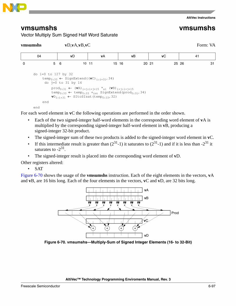
AltiVec Instructions
AltiVec™ Technology Programming Enviroments Manual, Rev. 3
Freescale Semiconductor 6-97
vmsumshs vmsumshsVector Multiply Sum Signed Half Word Saturate
vmsumshs vD,vA,vB,vC Form: VA
do i=0 to 127 by 32temp0:33 ← SignExtend((vC)i:i+31,34) do j=0 to 31 by 16
prod0:31 ← (vA)i+j:i+j+15 *si (vB)i+j:i+j+15temp0:33 ← temp0:33 +int SignExtend(prod0:31,34)vDi:i+31 ← SItoSIsat(temp0:33,32)
end
end
For each word element in vC the following operations are performed in the order shown.• Each of the two signed-integer half-word elements in the corresponding word element of vA is
multiplied by the corresponding signed-integer half-word element in vB, producing a signed-integer 32-bit product.
• The signed-integer sum of these two products is added to the signed-integer word element in vC.• If this intermediate result is greater than (231-1) it saturates to (231-1) and if it is less than -231 it
saturates to -231.• The signed-integer result is placed into the corresponding word element of vD.
Other registers altered:• SAT
Figure 6-70 shows the usage of the vmsumshs instruction. Each of the eight elements in the vectors, vA and vB, are 16 bits long. Each of the four elements in the vectors, vC and vD, are 32 bits long.
Figure 6-70. vmsumshs—Multiply-Sum of Signed Integer Elements (16- to 32-Bit)
04 vD vA vB vC 41
0 5 6 10 11 15 16 20 21 25 26 31
vA
vB
Prod
vC
vD
* * * * * * *
+ + + +
*

AltiVec Instructions
AltiVec™ Technology Programming Enviroments Manual, Rev. 3
6-98 Freescale Semiconductor
vmsumubm vmsumubmVector Multiply Sum Unsigned Byte Modulo
vmsumubm vD,vA,vB,vC Form: VA
do i=0 to 127 by 32
temp0:31 ← (vC)i:i+31 do j=0 to 31 by 8
prod0:15 ← (vA)i+j:i+j+7 *ui (vB)i+j:i+j+7temp0:32 ← temp0:32 +int ZeroExtend(prod0:15,32)vDi:i+31 ← temp0:31
end
end
For each word element in vC the following operations are performed in the order shown.• Each of the four unsigned-integer byte elements contained in the corresponding word element of
vA is multiplied by the corresponding unsigned-integer byte element in vB, producing an unsigned-integer 16-bit product.
• The unsigned-integer modulo sum of these four products is added to the unsigned-integer word element in vC.
• The unsigned-integer result is placed into the corresponding word element of vD.
Other registers altered:• None
Figure 6-71 shows the usage of the vmsumubm instruction. Each of the sixteen elements in the vectors, vA and vB, are 8 bits long. Each of the four elements in the vectors, vC and vD, are 32 bits long.
Figure 6-71. vmsumubm—Multiply-Sum of Unsigned Integer Elements (8- to 32-Bit)
04 vD vA vB vC 36
0 5 6 10 11 15 16 20 21 25 26 31
vA
vB
Prod
vC
vD
* * * * * * * * * * * * * * * *
+ + + +

AltiVec Instructions
AltiVec™ Technology Programming Enviroments Manual, Rev. 3
Freescale Semiconductor 6-99
vmsumuhm vmsumuhmVector Multiply Sum Unsigned Half Word Modulo
vmsumuhm vD,vA,vB,vC Form: VA
do i=0 to 127 by 32
temp0:31 ← (vC)i:i+31 do j=0 to 31 by 16
prod0:31 ← (vA)i+j:i+j+15 *ui (vB)i+j:i+j+15temp0:31 ← temp0:31 +int prod0:31vDi:i+31 ← temp2:33
end
end
For each word element in vC the following operations are performed in the order shown.• Each of the two unsigned-integer half-word elements contained in the corresponding word element
of vA is multiplied by the corresponding unsigned-integer half-word element in vB, producing a unsigned-integer 32-bit product.
• The unsigned-integer sum of these two products is added to the unsigned-integer word element in vC.
• The unsigned-integer result is placed into the corresponding word element of vD.
Other registers altered:• None
Figure 6-72 shows the usage of the vmsumuhm instruction. Each of the eight elements in the vectors, vA and vB, are 16 bits long. Each of the four elements in the vectors, vC and vD, are 32 bits long.
Figure 6-72. vmsumuhm—Multiply-Sum of Unsigned Integer Elements (16- to 32-Bit)
04 vD vA vB vC 38
0 5 6 10 11 15 16 20 21 25 26 31
vA
vB
Prod
vC
vD
* * * * * * *
+ + + +
*

AltiVec Instructions
AltiVec™ Technology Programming Enviroments Manual, Rev. 3
6-100 Freescale Semiconductor
vmsumuhs vmsumuhsVector Multiply Sum Unsigned Half Word Saturate
vmsumuhs vD,vA,vB,vC Form: VA
do i=0 to 127 by 32
temp0:33 ← ZeroExtend((vC)i:i+31,34) do j=0 to 31 by 16
prod0:31 ← (vA)i+j:i+j+15 *ui (vB)i+j:i+j+15temp0:33 ← temp0:33 +int ZeroExtend(prod0:31,34)vDi:i+31 ← UItoUIsat(temp0:33,32)
end
end
For each word element in vC the following operations are performed in the order shown.• Each of the two unsigned-integer half-word elements contained in the corresponding word element
of vA is multiplied by the corresponding unsigned-integer half-word element in vB, producing an unsigned-integer 32-bit product.
• The unsigned-integer sum of these two products is saturate-added to the unsigned-integer word element in vC.
• The unsigned-integer result is placed into the corresponding word element of vD.
Other registers altered:• SAT
Figure 6-73 shows the usage of the vmsumuhs instruction. Each of the eight elements in the vectors, vA and vB, are 16 bits long. Each of the four elements in the vectors, vC and vD, are 32 bits long.
Figure 6-73. vmsumuhs—Multiply-Sum of Unsigned Integer Elements (16- to 32-Bit)
04 vD vA vB vC 39
0 5 6 10 11 15 16 20 21 25 26 31
vA
vB
Prod
vC
vD
* * * * * * *
+ + + +
*

AltiVec Instructions
AltiVec™ Technology Programming Enviroments Manual, Rev. 3
Freescale Semiconductor 6-101
vmulesb vmulesbVector Multiply Even Signed Byte
vmulesb vD,vA,vB Form: VX
do i=0 to 127 by 16prod0:15 ← (vA)i:i+7 *si (vB)i:i+7 vDi:i+15 ← prod0:15
end
Each even-numbered signed-integer byte element in vA is multiplied by the corresponding signed-integer byte element in vB. The eight 16-bit signed-integer products are placed, in the same order, into the eight half words of vD.
Other registers altered:• None
Figure 6-74 shows the usage of the vmulesb instruction. Each of the sixteen elements in the vectors, vA and vB, is 8 bits long. Each of the eight elements in the vector, vD, is 16 bits long.
Figure 6-74. vmulesb—Even Multiply of Eight Signed Integer Elements (8-Bit)
04 vD vA vB 776
0 5 6 10 11 15 16 20 21 31
** * * * * * *
vA
vB
vD
ØØØØØØØØ
ØØØØØØØØ

AltiVec Instructions
AltiVec™ Technology Programming Enviroments Manual, Rev. 3
6-102 Freescale Semiconductor
vmulesh vmuleshVector Multiply Even Signed Half Word
vmulesh vD,vA,vB Form: VX
do i=0 to 127 by 32prod0:31 ← (vA)i:i+15 *si (vB)i:i+15vDi:i+31 ← prod0:31
end
Each even-numbered signed-integer half-word element in vA is multiplied by the corresponding signed-integer half-word element in vB. The four 32-bit signed-integer products are placed, in the same order, into the four words of vD.
Other registers altered:• None
Figure 6-75 shows the usage of the vmulesh instruction. Each of the eight elements in the vectors, vA and vB, is 16 bits long. Each of the four elements in the vector, vD, is 32 bits long.
Figure 6-75. vmulesh—Even Multiply of Four Signed Integer Elements (16-Bit)
04 vD vA vB 840
0 5 6 10 11 15 16 20 21 31
ØØØØ
*
vA
vB
vD
ØØØØ
***

AltiVec Instructions
AltiVec™ Technology Programming Enviroments Manual, Rev. 3
Freescale Semiconductor 6-103
vmuleub vmuleubVector Multiply Even Unsigned Byte
vmuleub vD,vA,vB Form: VX
do i=0 to 127 by 16prod0:15 ← (vA)i:i+7 *ui (vB)i:i+7(vD)i:i+15 ← prod0:15
end
Each even-numbered unsigned-integer byte element in register vA is multiplied by the corresponding unsigned-integer byte element in register vB. The eight 16-bit unsigned-integer products are placed, in the same order, into the eight half words of register vD.
Other registers altered:• None
Figure 6-76 shows the usage of the vmuleub instruction. Each of the sixteen elements in the vectors, vA and vB, is 8 bits long. Each of the eight elements in the vector, vD, is 16 bits long.
Figure 6-76. vmuleub—Even Multiply of Eight Unsigned Integer Elements (8-Bit)
04 vD vA vB 520
0 5 6 10 11 15 16 20 21 31
** * * * * * *
vA
vB
vD
ØØØØØØØØ
ØØØØØØØØ

AltiVec Instructions
AltiVec™ Technology Programming Enviroments Manual, Rev. 3
6-104 Freescale Semiconductor
vmuleuh vmuleuhVector Multiply Even Unsigned Half Word
vmuleuh vD,vA,vB Form: VX
do i=0 to 127 by 32prod0:31 ← (vA)i:i+15 *ui (vB)i:i+15(vD)i:i+31 ← prod0:31
end
Each even-numbered unsigned-integer half-word element in register vA is multiplied by the corresponding unsigned-integer half-word element in register vB. The four 32-bit unsigned-integer products are placed, in the same order, into the four words of register vD.
Other registers altered:• None
Figure 6-77 shows the usage of the vmuleuh instruction. Each of the eight elements in the vectors, vA and vB, is 16 bits long. Each of the four elements in the vector, vD, is 32 bits long.
Figure 6-77. vmuleuh—Even Multiply of Four Unsigned Integer Elements (16-Bit)
04 vD vA vB 584
0 5 6 10 11 15 16 20 21 31
ØØØØ
*
vA
vB
vD
ØØØØ
***
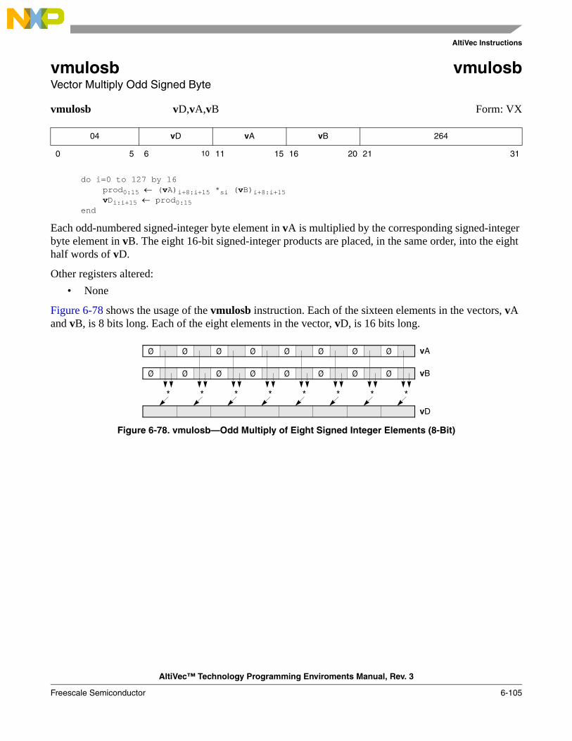
AltiVec Instructions
AltiVec™ Technology Programming Enviroments Manual, Rev. 3
Freescale Semiconductor 6-105
vmulosb vmulosbVector Multiply Odd Signed Byte
vmulosb vD,vA,vB Form: VX
do i=0 to 127 by 16prod0:15 ← (vA)i+8:i+15 *si (vB)i+8:i+15vDi:i+15 ← prod0:15
end
Each odd-numbered signed-integer byte element in vA is multiplied by the corresponding signed-integer byte element in vB. The eight 16-bit signed-integer products are placed, in the same order, into the eight half words of vD.
Other registers altered:• None
Figure 6-78 shows the usage of the vmulosb instruction. Each of the sixteen elements in the vectors, vA and vB, is 8 bits long. Each of the eight elements in the vector, vD, is 16 bits long.
Figure 6-78. vmulosb—Odd Multiply of Eight Signed Integer Elements (8-Bit)
04 vD vA vB 264
0 5 6 10 11 15 16 20 21 31
* *******
vA
vB
vD
Ø Ø Ø Ø Ø Ø Ø Ø
Ø Ø Ø Ø Ø Ø Ø Ø

AltiVec Instructions
AltiVec™ Technology Programming Enviroments Manual, Rev. 3
6-106 Freescale Semiconductor
vmulosh vmuloshVector Multiply Odd Signed Half Word
vmulosh vD,vA,vB Form: VX
do i=0 to 127 by 32prod0:31 ← (vA)i+16:i+31 *si (vB)i+16:i+31vDi:i+31 ← prod0:31
end
Each odd-numbered signed-integer half-word element in vA is multiplied by the corresponding signed-integer half-word element in vB. The four 32-bit signed-integer products are placed, in the same order, into the four words of vD.
Other registers altered:• None
Figure 6-79 shows the usage of the vmuleuh instruction. Each of the eight elements in the vectors, vA and vB, is 16 bits long. Each of the four elements in the vector, vD, is 32 bits long.
Figure 6-79. vmuleuh—Odd Multiply of Four Unsigned Integer Elements (16-Bit)
04 vD vA vB 328
0 5 6 10 11 15 16 20 21 31
Ø Ø Ø Ø
****
vA
vB
vD
Ø Ø Ø Ø

AltiVec Instructions
AltiVec™ Technology Programming Enviroments Manual, Rev. 3
Freescale Semiconductor 6-107
vmuloub vmuloubVector Multiply Odd Unsigned Byte
vmuloub vD,vA,vB Form: VX
do i=0 to 127 by 8prod0:15 ← (vA)i+8:i+15 *ui (vB)i+n:i+15vDi:i+15 ← prod0:15
end
Each odd-numbered unsigned-integer byte element in vA is multiplied by the corresponding unsigned-integer byte element in vB. The eight 16-bit unsigned-integer products are placed, in the same order, into the eight half words of vD.
Other registers altered:• None
Figure 6-80 shows the usage of the vmuloub instruction. Each of the sixteen elements in the vectors, vA and vB, is 8 bits long. Each of the eight elements in the vector, vD, is 16 bits long.
Figure 6-80. vmuloub—Odd Multiply of Eight Unsigned Integer Elements (8-Bit)
04 vD vA vB 8
0 5 6 10 11 15 16 20 21 31
* *******
vA
vB
vD
Ø Ø Ø Ø Ø Ø Ø Ø
Ø Ø Ø Ø Ø Ø Ø Ø
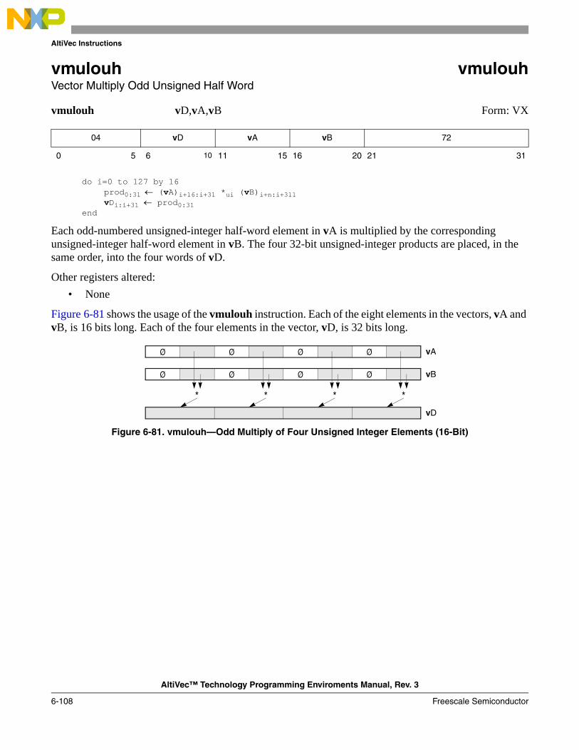
AltiVec Instructions
AltiVec™ Technology Programming Enviroments Manual, Rev. 3
6-108 Freescale Semiconductor
vmulouh vmulouhVector Multiply Odd Unsigned Half Word
vmulouh vD,vA,vB Form: VX
do i=0 to 127 by 16prod0:31 ← (vA)i+16:i+31 *ui (vB)i+n:i+311vDi:i+31 ← prod0:31
end
Each odd-numbered unsigned-integer half-word element in vA is multiplied by the corresponding unsigned-integer half-word element in vB. The four 32-bit unsigned-integer products are placed, in the same order, into the four words of vD.
Other registers altered:• None
Figure 6-81 shows the usage of the vmulouh instruction. Each of the eight elements in the vectors, vA and vB, is 16 bits long. Each of the four elements in the vector, vD, is 32 bits long.
Figure 6-81. vmulouh—Odd Multiply of Four Unsigned Integer Elements (16-Bit)
04 vD vA vB 72
0 5 6 10 11 15 16 20 21 31
Ø Ø Ø Ø
****
vA
vB
vD
Ø Ø Ø Ø

AltiVec Instructions
AltiVec™ Technology Programming Enviroments Manual, Rev. 3
Freescale Semiconductor 6-109
vnmsubfp vnmsubfpVector Negative Multiply-Subtract Floating-Point
vnmsubfp vD,vA,vC,vB Form: VA
do i=0 to 127 by 32vDi:i+31 ← -RndToNearFP32(((vA)i:i+31 *fp (vC)i:i+31) -fp (vB)i:i+31)
end
Each single-precision floating-point word element in vA is multiplied by the corresponding single-precision floating-point word element in vC. The corresponding single-precision floating-point word element in vB is subtracted from the product. The sign of the difference is inverted. The result is rounded to the nearest single-precision floating-point number and placed into the corresponding word element of vD.
Note that only one rounding occurs in this operation. Also note that a QNaN result is not negated.
Other registers altered:• None
Figure 6-82 shows the usage of the vnmsubfp instruction. Each of the four elements in the vectors, vA, vB, and vD, is 32 bits long.
Figure 6-82. vnmsubfp—Negative Multiply-Subtract of Four Floating-Point Elements (32-Bit)
04 vD vA vB vC 47
0 5 6 10 11 15 16 20 21 25 26 31
-
vA
vC
Prod
vB
Invert &
* * * *
- - -
vD
Round
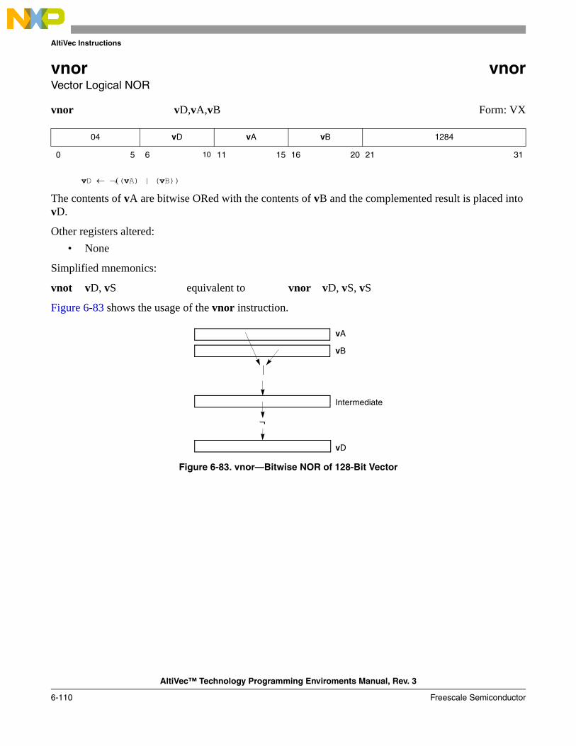
AltiVec Instructions
AltiVec™ Technology Programming Enviroments Manual, Rev. 3
6-110 Freescale Semiconductor
vnor vnor Vector Logical NOR
vnor vD,vA,vB Form: VX
vD ← ¬((vA) | (vB))
The contents of vA are bitwise ORed with the contents of vB and the complemented result is placed into vD.
Other registers altered:• None
Simplified mnemonics:
vnot vD, vS equivalent to vnor vD, vS, vS
Figure 6-83 shows the usage of the vnor instruction.
Figure 6-83. vnor—Bitwise NOR of 128-Bit Vector
04 vD vA vB 1284
0 5 6 10 11 15 16 20 21 31
|
vB
Intermediate
vA
vD
¬

AltiVec Instructions
AltiVec™ Technology Programming Enviroments Manual, Rev. 3
Freescale Semiconductor 6-111
vor vorVector Logical OR
vor vD,vA,vB Form: VX
vD ← (vA) | (vB)
The contents of vA are ORed with the contents of vB and the result is placed into vD.
Other registers altered:• None
Simplified mnemonics:
vmr vD, vS equivalent to vor vD, vS, vS
Figure 6-84 shows the usage of the vor instruction.
Figure 6-84. vor—Bitwise OR of 128-Bit Vector
04 vD vA vB 1156
0 5 6 10 11 15 16 20 21 31
|
vB
vA
vD

AltiVec Instructions
AltiVec™ Technology Programming Enviroments Manual, Rev. 3
6-112 Freescale Semiconductor
vperm vpermVector Permute
vperm vD,vA,vB,vC Form: VA
temp0:255 ← (vA) || (vB)do i=0 to 127 by 8
b ← (vC)i+3:i+7 || 0b000vDi:i+7 ← tempb:b+7
end
Let the source vector be the concatenation of the contents of vA followed by the contents of vB. For each integer i in the range 0–15, the contents of the byte element in the source vector specified in bits 3–7 of byte element i in vC are placed into byte element i of vD.
Other registers altered:• None
Programming note: See the programming notes with the Load Vector for Shift Left and Load Vector for Shift Right instructions for examples of usage on the vperm instruction.
Figure 6-85 shows the usage of the vperm instruction. Each of the sixteen elements in the vectors, vA, vB, vC, and vD, is 8 bits long.
Figure 6-85. vperm—Concatenate Sixteen Integer Elements (8-Bit)
04 vD vA vB vC 43
0 5 6 10 11 15 16 20 21 25 26 31
vC1 14 18 10 16 15 19 1A 1C 1C 1C 13 8 1D 1B 0E
vA
vB
vD
0 1 2 3 4 5 6 7 8 9 A B C D E F
10 12 13 14 15 16 17 18 19 1A 1B 1C 1D 1F11 1E

AltiVec Instructions
AltiVec™ Technology Programming Enviroments Manual, Rev. 3
Freescale Semiconductor 6-113
vpkpx vpkpxVector Pack Pixel32
vpkpx vD,vA,vB Form: VX
do i=0 to 63 by 16
vDi ← (vA)i*2+7vDi+1:i+5 ← (vA)(i*2)+8:(i*2)+12vDi+6:i+1 ← (vA)(i*2)+16:(i*2)+20vDi+11:i+15 ← (vA)((i*2)+24:(i*2)+28vDi+64 ← (vB)(i*2)+7vDi+65:i+69 ← (vB)(i*2)+8:(i*2)+12vDi+70:i+74 ← (vB)(i*2)+16:(i*2)+20vDi+75:i+79 ← (vB)(i*2)+24:(i*2)+28
end
The source vector is the concatenation of the contents of vA followed by the contents of vB. Each 32-bit word element in the source vector is packed to produce a 16-bit half-word value as described below and placed into the corresponding half-word element of vD. A word is packed to 16 bits by concatenating, in order, the following bits.
• Bit 7 of the first byte (bit 7 of the word)• Bits 0–4 of the second byte (bits 8–12 of the word)• Bits 0–4 of the third byte (bits 16–20 of the word)• Bits 0–4 of the fourth byte (bits 24–28 of the word)
Figure 6-86 shows which bits of the source word are packed to form the half word in the destination register.
Figure 6-86. vpkpx—How a Word is Packed to a Half Word
Other registers altered:• None
04 vD vA vB 782
0 5 6 10 11 15 16 20 21 31
Source Word
0 1 2 3 4 5 6 7 8 9 10 11 12 13 14 15 16 17 18 19 20 21 22 23 24 25 26 27 28 29 30 31
vD Packed Half Word
0 1 2 3 4 5 6 7 8 9 10 11 12 13 14 15
7 8 9 10 11 12 16 17 18 19 20 24 25 26 27 28

AltiVec Instructions
AltiVec™ Technology Programming Enviroments Manual, Rev. 3
6-114 Freescale Semiconductor
Programming Note: Each source word can be considered to be a 32-bit pixel consisting of four 8-bit channels. Each target half word can be considered to be a 16-bit pixel consisting of one 1-bit channel and three 5-bit channels. A channel can be used to specify the intensity of a particular color, such as red, green, or blue, or to provide other information needed by the application.
Figure 6-87 shows the usage of the vpkpx instruction. Each of the four elements in the vectors, vA and vB, is 32 bits long. Each of the eight elements in the vector, vD, is 16 bits long.
Figure 6-87. vpkpx—Pack Eight Elements (32-Bit) to Eight Elements (16-Bit)
vA vB
vD

AltiVec Instructions
AltiVec™ Technology Programming Enviroments Manual, Rev. 3
Freescale Semiconductor 6-115
vpkshss vpkshssVector Pack Signed Half Word Signed Saturate
vpkshss vD,vA,vB Form: VX
do i=0 to 63 by 8vDi:i+7 ← SItoSIsat((vA)i*2:(i*2)+15,8)vDi+64:i+71 ← SItoSIsat((vB)i*2:(i*2)+15,8)
end
Let the source vector be the concatenation of the contents of vA followed by the contents of vB.
Each signed integer half-word element in the source vector is converted to an 8-bit signed integer. If the value of the element is greater than (2 7-1) the result saturates to (27-1) and if the value is less than -27 the result saturates to -27. The result is placed into the corresponding byte element of vD.
Other registers altered:• SAT
Figure 6-88 shows the usage of the vpkshss instruction. Each of the eight elements in the vectors, vA and vB, is 16 bits long. Each of the sixteen elements in the vector, vD, is 8 bits long.
Figure 6-88. vpkshss—Pack Sixteen Signed Integer Elements (16-Bit) to Sixteen Signed Integer Elements (8-Bit)
04 vD vA vB 398
0 5 6 10 11 15 16 20 21 31
vA vB
vD

AltiVec Instructions
AltiVec™ Technology Programming Enviroments Manual, Rev. 3
6-116 Freescale Semiconductor
vpkshus vpkshusVector Pack Signed Half Word Unsigned Saturate
vpkshus vD,vA,vB Form: VX
do i=0 to 63 by 8vDi:i+7 ← SItoUIsat((vA)i*2:(i*2)+7,8)vDi+64:i+71 ← SItoUIsat((vB)i*2:(i*2)+7,8)
end
Let the source vector be the concatenation of the contents of vA followed by the contents of vB.
Each signed integer half-word element in the source vector is converted to an 8-bit unsigned integer. If the value of the element is greater than (28-1) the result saturates to (28-1) and if the value is less than 0 the result saturates to 0. The result is placed into the corresponding byte element of vD.
Other registers altered:• SAT
Figure 6-89 shows the usage of the vpkshus instruction. Each of the eight elements in the vectors, vA and vB, is 16 bits long. Each of the sixteen elements in the vector, vD, is 8 bits long.
Figure 6-89. vpkshus—Pack Sixteen Signed Integer Elements (16-Bit) to Sixteen Unsigned Integer Elements (8-Bit)
04 vD vA vB 270
0 5 6 10 11 15 16 20 21 31
vA vB
vD

AltiVec Instructions
AltiVec™ Technology Programming Enviroments Manual, Rev. 3
Freescale Semiconductor 6-117
vpkswss vpkswssVector Pack Signed Word Signed Saturate
vpkswss vD,vA,vB Form: VX
do i=0 to 63 by 16vDi:i+15 ← SItoSIsat((vA)i*2:(i*2)+31,16)vDi+64:i+79 ← SItoSIsat((vB)i*2:(i*2)+31,16)
end
Let the source vector be the concatenation of the contents of vA followed by the contents of vB.
Each signed integer word element in the source vector is converted to a 16-bit signed integer half word. If the value of the element is greater than (215-1) the result saturates to (215-1) and if the value is less than -215 the result saturates to -215. The result is placed into the corresponding half-word element of vD.
Other registers altered:• SAT
Figure 6-90 shows the usage of the vpkswss instruction. Each of the four elements in the vectors, vA and vB, is 32 bits long. Each of the eight elements in the vector, vD, is 16 bits long.
g
Figure 6-90. vpkswss—Pack Eight Signed Integer Elements (32-Bit) to Eight Signed Integer Elements (16-Bit)
04 vD vA vB 462
0 5 6 10 11 15 16 20 21 31
vA vB
vD
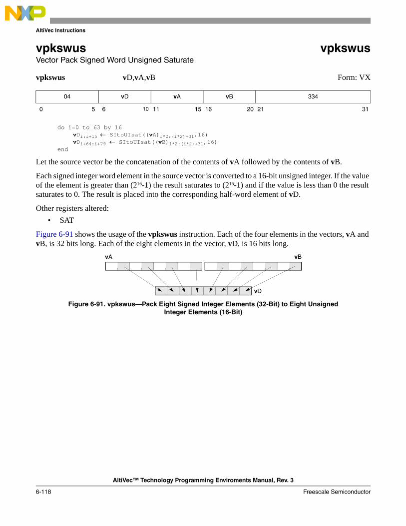
AltiVec Instructions
AltiVec™ Technology Programming Enviroments Manual, Rev. 3
6-118 Freescale Semiconductor
vpkswus vpkswusVector Pack Signed Word Unsigned Saturate
vpkswus vD,vA,vB Form: VX
do i=0 to 63 by 16vDi:i+15 ← SItoUIsat((vA)i*2:(i*2)+31,16)vDi+64:i+79 ← SItoUIsat((vB)i*2:(i*2)+31,16)
end
Let the source vector be the concatenation of the contents of vA followed by the contents of vB.
Each signed integer word element in the source vector is converted to a 16-bit unsigned integer. If the value of the element is greater than (216-1) the result saturates to (216-1) and if the value is less than 0 the result saturates to 0. The result is placed into the corresponding half-word element of vD.
Other registers altered:• SAT
Figure 6-91 shows the usage of the vpkswus instruction. Each of the four elements in the vectors, vA and vB, is 32 bits long. Each of the eight elements in the vector, vD, is 16 bits long.
Figure 6-91. vpkswus—Pack Eight Signed Integer Elements (32-Bit) to Eight Unsigned Integer Elements (16-Bit)
04 vD vA vB 334
0 5 6 10 11 15 16 20 21 31
vA vB
vD
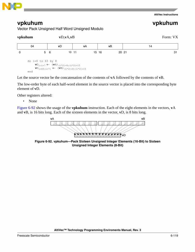
AltiVec Instructions
AltiVec™ Technology Programming Enviroments Manual, Rev. 3
Freescale Semiconductor 6-119
vpkuhum vpkuhumVector Pack Unsigned Half Word Unsigned Modulo
vpkuhum vD,vA,vB Form: VX
do i=0 to 63 by 8vDi:i+7 ← (vA)(i*2)+8:(i*2)+15vDi+64:i+71 ← (vB)(i*2)+8:(i*2)+15
end
Let the source vector be the concatenation of the contents of vA followed by the contents of vB.
The low-order byte of each half-word element in the source vector is placed into the corresponding byte element of vD.
Other registers altered:• None
Figure 6-92 shows the usage of the vpkuhum instruction. Each of the eight elements in the vectors, vA and vB, is 16 bits long. Each of the sixteen elements in the vector, vD, is 8 bits long.
Figure 6-92. vpkuhum—Pack Sixteen Unsigned Integer Elements (16-Bit) to Sixteen Unsigned Integer Elements (8-Bit)
04 vD vA vB 14
0 5 6 10 11 15 16 20 21 31
vA vB
vD

AltiVec Instructions
AltiVec™ Technology Programming Enviroments Manual, Rev. 3
6-120 Freescale Semiconductor
vpkuhus vpkuhusVector Pack Unsigned Half Word Unsigned Saturate
vpkuhus vD,vA,vB Form: VX
do i=0 to 63 by 8vDi:i+7 ← UItoUIsat((vA)i*2:(i*2)+15,8)vDi+64:i+71 ← UItoUIsat((vB)i*2:(i*2)+15,8)
end
Let the source vector be the concatenation of the contents of vA followed by the contents of vB.
Each unsigned integer half-word element in the source vector is converted to an 8-bit unsigned integer. If the value of the element is greater than (28-1) the result saturates to (28-1). The result is placed into the corresponding byte element of vD.
Other registers altered:• SAT
Figure 6-93 shows the usage of the vpkuhus instruction. Each of the eight elements in the vectors, vA and vB, is 16 bits long. Each of the sixteen elements in the vector, vD, is 8 bits long.
Figure 6-93. vpkuhus—Pack Sixteen Unsigned Integer Elements (16-Bit) to Sixteen Unsigned Integer Elements (8-Bit)
04 vD vA vB 142
0 5 6 10 11 15 16 20 21 31
vD
UItoUIsat
vBvA
UItoUIsat UItoUIsat UItoUIsat UItoUIsat UItoUIsat UItoUIsat UItoUIsat UItoUIsat UItoUIsat UItoUIsat UItoUIsat UItoUIsat UItoUIsat UItoUIsat UItoUIsat
vTempA vTempB

AltiVec Instructions
AltiVec™ Technology Programming Enviroments Manual, Rev. 3
Freescale Semiconductor 6-121
vpkuwum vpkuwumVector Pack Unsigned Word Unsigned Modulo
vpkuwum vD,vA,vB Form: VX
do i=0 to 63 by 16vDi:i+15 ← (vA)(i*2)+16:(i*2)+31vDi+64:i+79 ← (vB)(i*2)+16:(i*2)+31
end
Let the source vector be the concatenation of the contents of vA followed by the contents of vB.
The low-order half word of each word element in the source vector is placed into the corresponding half-word element of vD.
Other registers altered:• None
Figure 6-94 shows the usage of the vpkuwum instruction. Each of the four elements in the vectors, vA and vB, is 32 bits long. Each of the eight elements in the vector, vD, is 16 bits long.
Figure 6-94. vpkuwum—Pack Eight Unsigned Integer Elements (32-Bit) to Eight Unsigned Integer Elements (16-Bit)
04 vD vA vB 78
0 5 6 10 11 15 16 20 21 31
vA vB
vD

AltiVec Instructions
AltiVec™ Technology Programming Enviroments Manual, Rev. 3
6-122 Freescale Semiconductor
vpkuwus vpkuwusVector Pack Unsigned Word Unsigned Saturate
vpkuwus vD,vA,vB Form: VX
do i=0 to 63 by 16vDi:i+15 ← UItoUIsat((vA)i*2:(i*2)+31,16)vDi+64:i+79 ← UItoUIsat((vB)i*2:(i*2)+31,16)
end
Let the source vector be the concatenation of the contents of vA followed by the contents of vB.
Each unsigned integer word element in the source vector is converted to a 16-bit unsigned integer. If the value of the element is greater than (216-1) the result saturates to (216-1). The result is placed into the corresponding half-word element of vD.
Other registers altered:• SAT
Figure 6-95 shows the usage of the vpkuwus instruction. Each of the four elements in the vectors, vA and vB, is 32 bits long. Each of the eight elements in the vector, vD, is 16 bits long.
Figure 6-95. vpkuwus—Pack Eight Unsigned Integer Elements (32-Bit) to Eight Unsigned Integer Elements (16-Bit)
04 vD vA vB 206
0 5 6 10 11 15 16 20 21 31
vA
vTempB
vD
vTempA
vB
UItoUIsat UItoUIsat UItoUIsat UItoUIsat UItoUIsatUItoUIsat UItoUIsat UItoUIsat

AltiVec Instructions
AltiVec™ Technology Programming Enviroments Manual, Rev. 3
Freescale Semiconductor 6-123
vrefp vrefpVector Reciprocal Estimate Floating-Point
vrefp vD,vB Form: VX
do i=0 to 127 by 32x ← (vB)i:i+31vDi:i+31 ← 1/x
end
The single-precision floating-point estimate of the reciprocal of each single-precision floating-point element in vB is placed into the corresponding element of vD.
For results that are not a +0, -0, +∞, -∞, or QNaN, the estimate has a relative error in precision no greater than one part in 4096, that is:
where x is the value of the element in vB. Note that the value placed into the element of vD may vary between implementations, and between different executions on the same implementation.
Operation with various special values of the element in vB is summarized below in Table 6-7.
If VSCR[NJ]=1, every denormalized operand element is truncated to a 0 of the same sign before the operation is carried out, and each denormalized result element truncates to a 0 of the same sign.
Other registers altered:• None
04 vD 0_0000 vB 266
0 5 6 10 11 15 16 20 21 31
Table 6-7. Special Values of the Element in vB
Value Result
–∞ –0
– 0 – ∞
+0 +∞
+∞ +0
NaN QNaN
estimate 1 x⁄–1 x⁄
------------------------------------------1
4096-------------≤
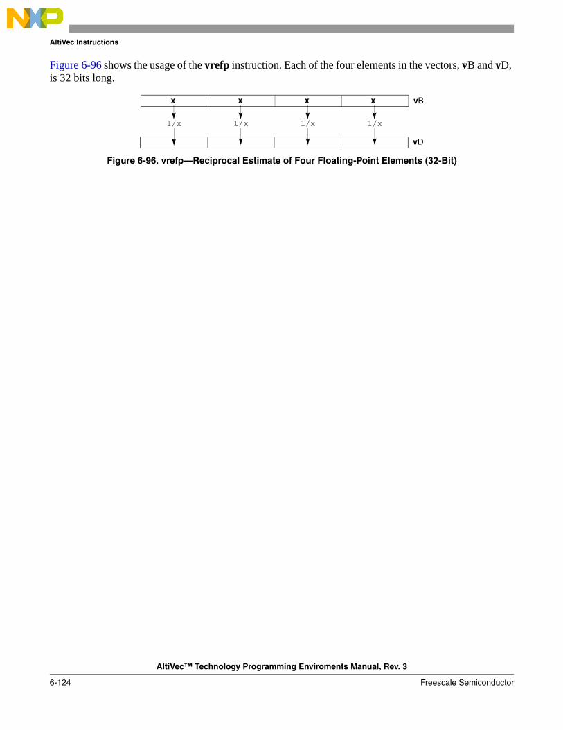
AltiVec Instructions
AltiVec™ Technology Programming Enviroments Manual, Rev. 3
6-124 Freescale Semiconductor
Figure 6-96 shows the usage of the vrefp instruction. Each of the four elements in the vectors, vB and vD, is 32 bits long.
Figure 6-96. vrefp—Reciprocal Estimate of Four Floating-Point Elements (32-Bit)
1/x1/x1/x1/x
vB
vD
x x x x
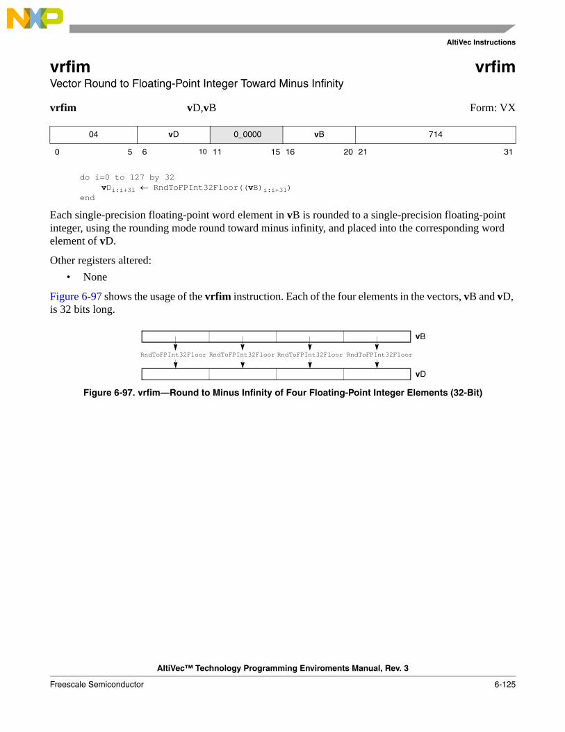
AltiVec Instructions
AltiVec™ Technology Programming Enviroments Manual, Rev. 3
Freescale Semiconductor 6-125
vrfim vrfimVector Round to Floating-Point Integer Toward Minus Infinity
vrfim vD,vB Form: VX
do i=0 to 127 by 32vDi:i+31 ← RndToFPInt32Floor((vB)i:i+31)
end
Each single-precision floating-point word element in vB is rounded to a single-precision floating-point integer, using the rounding mode round toward minus infinity, and placed into the corresponding word element of vD.
Other registers altered:• None
Figure 6-97 shows the usage of the vrfim instruction. Each of the four elements in the vectors, vB and vD, is 32 bits long.
Figure 6-97. vrfim—Round to Minus Infinity of Four Floating-Point Integer Elements (32-Bit)
04 vD 0_0000 vB 714
0 5 6 10 11 15 16 20 21 31
RndToFPInt32FloorRndToFPInt32FloorRndToFPInt32FloorRndToFPInt32Floor
vB
vD

AltiVec Instructions
AltiVec™ Technology Programming Enviroments Manual, Rev. 3
6-126 Freescale Semiconductor
vrfin vrfinVector Round to Floating-Point Integer Nearest
vrfin vD,vB Form: VX
do i=0 to 127 by 32vDi:i+31 ← RndToFPInt32Near((vB)i:i+31)
end
Each single-precision floating-point word element in vB is rounded to a single-precision floating-point integer, using the rounding mode round to nearest, and placed into the corresponding word element of vD.
Note the result is independent of VSCR[NJ].
Other registers altered:• None
Figure 6-98 shows the usage of the vrfin instruction. Each of the four elements in the vectors, vB and vD, is 32 bits long.
Figure 6-98. vrfin—Nearest Round to Nearest of Four Floating-Point Integer Elements (32-Bit)
04 vD 0_0000 vB 522
0 5 6 10 11 15 16 20 21 31
RndToFPInt32NearRndToFPInt32NearRndToFPInt32NearRndToFPInt32Near
vB
vD

AltiVec Instructions
AltiVec™ Technology Programming Enviroments Manual, Rev. 3
Freescale Semiconductor 6-127
vrfip vrfipVector Round to Floating-Point Integer Toward Plus Infinity
vrfip vD,vB Form: VX
do i=0 to 127 by 32vDi:i+31 ← RndToFPInt32Ceil((vB)i:i+31)
end
Each single-precision floating-point word element in vB is rounded to a single-precision floating-point integer, using the rounding mode round toward plus infinity, and placed into the corresponding word element of vD.
If VSCR[NJ]=1, every denormalized operand element is truncated to 0 before the comparison is made.
Other registers altered:• None
Figure 6-99 shows the usage of the vrfip instruction. Each of the four elements in the vectors, vB and vD, is 32 bits long.
Figure 6-99. vrfip—Round to Plus Infinity of Four Floating-Point Integer Elements (32-Bit)
04 vD 0_0000 vB 650
0 5 6 10 11 15 16 20 21 31
RndToFPInt32CeilRndToFPInt32CeilRndToFPInt32CeilRndToFPInt32Ceil
vB
vD

AltiVec Instructions
AltiVec™ Technology Programming Enviroments Manual, Rev. 3
6-128 Freescale Semiconductor
vrfiz vrfizVector Round to Floating-Point Integer Toward Zero
vrfiz vD,vB Form: VX
do i=0 to 127 by 32vDi:i+31 ← RndToFPInt32Trunc((vB)i:i+31)
end
Each single-precision floating-point word element in vB is rounded to a single-precision floating-point integer, using the rounding mode round toward zero, and placed into the corresponding word element of vD.
Note, the result is independent of VSCR[NJ].
Other registers altered:• None
Figure 6-100 shows the usage of the vrfiz instruction. Each of the four elements in the vectors, vB and vD, is 32 bits long.
Figure 6-100. vrfiz—Round-to-Zero of Four Floating-Point Integer Elements (32-Bit)
04 vD 0_0000 vB 586
0 5 6 10 11 15 16 20 21 31
RndToFPInt32TruncRndToFPInt32TruncRndToFPInt32TruncRndToFPInt32Trunc
vB
vD

AltiVec Instructions
AltiVec™ Technology Programming Enviroments Manual, Rev. 3
Freescale Semiconductor 6-129
vrlb vrlbVector Rotate Left Integer Byte
vrlb vD,vA,vB Form: VX
do i=0 to 127 by 8sh ← (vB)i+5:i+7vDi:i+7 ← ROTL((vA)i:i+7,sh)
end
Each element is a byte. Each element in vA is rotated left by the number of bits specified in the low-order 3 bits of the corresponding element in vB. The result is placed into the corresponding element of vD.
Other registers altered:• None
Figure 6-101 shows the usage of the vrlb instruction. Each of the sixteen elements in the vectors, vA, vB, and vD, is 8 bits long.
Figure 6-101. vrlb—Left Rotate of Sixteen Integer Elements (8-Bit)
04 vD vA vB 4
0 5 6 10 11 15 16 20 21 31
vA
vD
Rotate left by the value specified in eachof vB element’s low-order 3 bits.

AltiVec Instructions
AltiVec™ Technology Programming Enviroments Manual, Rev. 3
6-130 Freescale Semiconductor
vrlh vrlhVector Rotate Left Integer Half Word
vrlh vD,vA,vB Form: VX
do i=0 to 127 by 16sh ← (vB)i+12:i+15vDi:i+15 ← ROTL((vA)i:i+15,sh)
end
Each element is a half word.
Each element in vA is rotated left by the number of bits specified in the low-order 4 bits of the corresponding element in vB. The result is placed into the corresponding element of vD.
Other registers altered:• None
Figure 6-102 shows the usage of the vrlh instruction. Each of the eight elements in the vectors, vA, vB, and vD, is 16 bits long.
Figure 6-102. vrlh—Left Rotate of Eight Integer Elements (16-Bit)
04 vD vA vB 68
0 5 6 10 11 15 16 20 21 31
vA
vD
Rotate left by the value specified in eachof vB element’s low-order 4 bits.
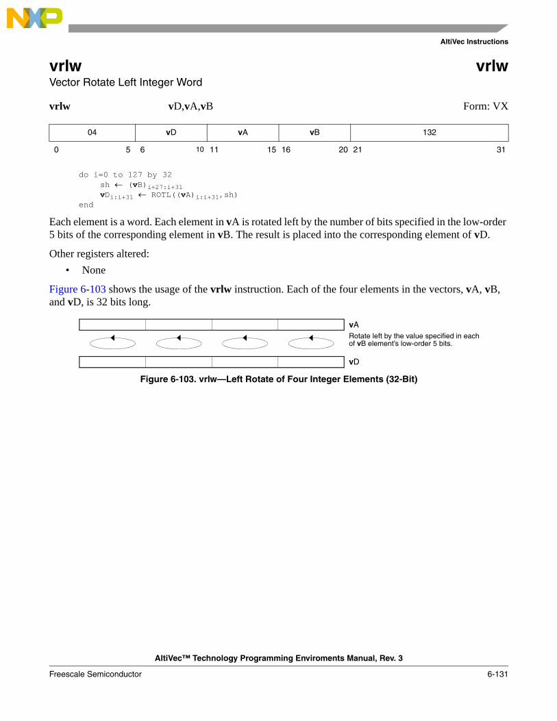
AltiVec Instructions
AltiVec™ Technology Programming Enviroments Manual, Rev. 3
Freescale Semiconductor 6-131
vrlw vrlwVector Rotate Left Integer Word
vrlw vD,vA,vB Form: VX
do i=0 to 127 by 32sh ← (vB)i+27:i+31vDi:i+31 ← ROTL((vA)i:i+31,sh)
end
Each element is a word. Each element in vA is rotated left by the number of bits specified in the low-order 5 bits of the corresponding element in vB. The result is placed into the corresponding element of vD.
Other registers altered:• None
Figure 6-103 shows the usage of the vrlw instruction. Each of the four elements in the vectors, vA, vB, and vD, is 32 bits long.
Figure 6-103. vrlw—Left Rotate of Four Integer Elements (32-Bit)
04 vD vA vB 132
0 5 6 10 11 15 16 20 21 31
vA
vD
Rotate left by the value specified in eachof vB element’s low-order 5 bits.

AltiVec Instructions
AltiVec™ Technology Programming Enviroments Manual, Rev. 3
6-132 Freescale Semiconductor
vrsqrtefp vrsqrtefpVector Reciprocal Square Root Estimate Floating-Point
vrsqrtefp vD,vB Form: VX
do i=0 to 127 by 32
x ← (vB)i:i+31vDi:i+31 ← 1 ÷fp (√fp(x))
end
The single-precision estimate of the reciprocal of the square root of each single-precision element in vB is placed into the corresponding word element of vD. The estimate has a relative error in precision no greater than one part in 4096, as explained below:
where x is the value of the element in vB. Note that the value placed into the element of vD may vary between implementations and between different executions on the same implementation. Operation with various special values of the element in vB is summarized below in Table 6-8.
Other registers altered:• None
Figure 6-104 shows the usage of the vrsqrtefp instruction. Each of the four elements in the vectors, vA, vB, and vD, is 32 bits long.
Figure 6-104. vrsqrtefp—Reciprocal Square Root Estimate of Four Floating-Point Elements (32-Bit)
04 vD 0_0000 vB 330
0 5 6 10 11 15 16 20 21 31
Table 6-8. Special Values of the Element in vB
Value Result Value Result
–∞ QNaN +0 +∞
less than 0 QNaN +∞ +0
–0 –∞ NaN QNaN
estimate 1 x⁄–1 x⁄
--------------------------------------------1
4096-------------≤
1 / √x
vB
vD
1 / √x1 / √x 1 / √x

AltiVec Instructions
AltiVec™ Technology Programming Enviroments Manual, Rev. 3
Freescale Semiconductor 6-133
vsel vselVector Conditional Select
vsel vD,vA,vB,vC Form: VA
do i=0 to 127if (vC)i=0 then vDi ← (vA)i else vDi ← (vB)i
end
For each bit in vC that contains the value 0, the corresponding bit in vA is placed into the corresponding bit of vD. For each bit in vC that contains the value 1, the corresponding bit in vB is placed into the corresponding bit of vD.
Other registers altered:• None
Figure 6-105 shows the usage of the vsel instruction. Each of the vectors, vA, vB, vC, and vD, is 128 bits long.
Figure 6-105. vsel—Bitwise Conditional Select of Vector Contents (128-Bit)
04 vD vA vB vC 42
0 5 6 10 11 15 16 20 21 25 26 31
vB
vA
vC0 1 0 0 1 1 0 0 • • • • • • • • • • •
vD
• • • • • • • • • • •
• • • • • • • • • • •
• • • • • • • • • • •
• • • • • • • • • • • •

AltiVec Instructions
AltiVec™ Technology Programming Enviroments Manual, Rev. 3
6-134 Freescale Semiconductor
vsl vslVector Shift Left
vsl vD,vA,vB Form: VX
sh ← (vB)125:127t ← 1do i = 0 to 127 by 8
t ← t & ((vB)i+5:i+7 = sh)if t = 1 then vD ← (vA) <<ui shelse vD ← undefined
end
The contents of vA are shifted left by the number of bits specified in vB[125–127]. Bits shifted out of bit 0 are lost. Zeros are supplied to the vacated bits on the right. The result is placed into vD.
The contents of the low-order three bits of all byte elements in vB must be identical to vB[125–127]; otherwise the value placed into vD is undefined.
Other registers altered:• None
Figure 6-106 shows the usage of the vsl instruction. In the example in Figure 6-106 the shift count specificed in vB[125–127] is 7 (0b111), that shift count is then put in the low-order three bits of all the byte elements in vB. In this example, the contents of vA are shifted left by 7 bits and replaced with zeros.
Figure 6-106. vsl—Shift Bits Left in Vector (128-Bit)
04 vD vA vB 452
0 5 6 10 11 15 16 20 21 31
vA
vD
• • • • • • • • • •
* 0b111 = 7 = sh = shift count
sh zeros
0000000
Shift left by sh bits
125 127
vB111 111 111 111 111 111 111 111 111 111 111 111 111 111 111 111*
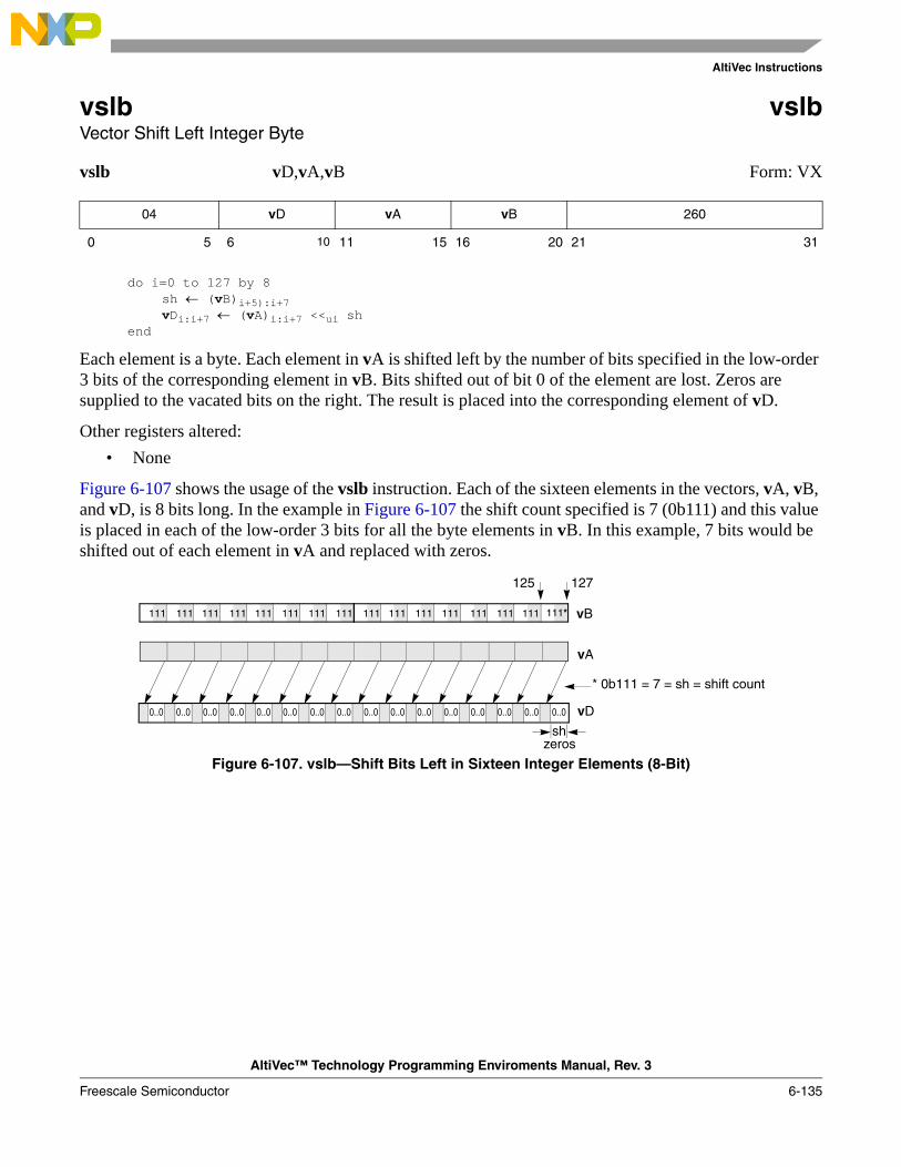
AltiVec Instructions
AltiVec™ Technology Programming Enviroments Manual, Rev. 3
Freescale Semiconductor 6-135
vslb vslbVector Shift Left Integer Byte
vslb vD,vA,vB Form: VX
do i=0 to 127 by 8sh ← (vB)i+5):i+7vDi:i+7 ← (vA)i:i+7 <<ui sh
end
Each element is a byte. Each element in vA is shifted left by the number of bits specified in the low-order 3 bits of the corresponding element in vB. Bits shifted out of bit 0 of the element are lost. Zeros are supplied to the vacated bits on the right. The result is placed into the corresponding element of vD.
Other registers altered:• None
Figure 6-107 shows the usage of the vslb instruction. Each of the sixteen elements in the vectors, vA, vB, and vD, is 8 bits long. In the example in Figure 6-107 the shift count specified is 7 (0b111) and this value is placed in each of the low-order 3 bits for all the byte elements in vB. In this example, 7 bits would be shifted out of each element in vA and replaced with zeros.
Figure 6-107. vslb—Shift Bits Left in Sixteen Integer Elements (8-Bit)
04 vD vA vB 260
0 5 6 10 11 15 16 20 21 31
vA
vD
* 0b111 = 7 = sh = shift count
0..0
shzeros
0..00..00..00..00..00..00..00..00..00..00..00..00..00..00..0
125 127
vB111 111 111 111 111 111 111 111 111 111 111 111 111 111 111 111*

AltiVec Instructions
AltiVec™ Technology Programming Enviroments Manual, Rev. 3
6-136 Freescale Semiconductor
vsldoi vsldoiVector Shift Left Double by Octet Immediate
vsldoi vD, vA, vB, SHB Form: VA
vD ← ((vA) || (vB)) <<ui (SHB || 0b000)
Let the source vector be the concatenation of the contents of vA followed by the contents of vB. Bytes SHB:SHB+15 of the source vector are placed into vD.
Other registers altered:• None
Figure 6-108 shows the usage of the vsldoi instruction. Each of the sixteen elements in the vectors, vA, vB, and vD, is 8 bits long.
Figure 6-108. vsldoi—Shift Left by Bytes Specified
04 vD vA vB 0 SHB 44
0 5 6 10 11 15 16 20 21 22 25 26 31
vA
vB
vD
SHB = Shift Count Bytes

AltiVec Instructions
AltiVec™ Technology Programming Enviroments Manual, Rev. 3
Freescale Semiconductor 6-137
vslh vslhVector Shift Left Integer Half Word
vslh vD,vA,vB Form: VX
do i=0 to 127 by 16sh ← (vB)i+12:i+15vDi:i+15 ← (vA)i:i+15 <<ui sh
end
Each element is a half word. Each element in vA is shifted left by the number of bits specified in the low-order 4 bits of the corresponding element in vB. Bits shifted out of bit 0 of the element are lost. Zeros are supplied to the vacated bits on the right. The result is placed into the corresponding element of vD.
Other registers altered:• None
Figure 6-109 shows the usage of the vslh instruction. Each of the eight elements in the vectors, vA, vB, and vD, is 16 bits long. For the example used in Figure 6-109 the shift count specificed in the low-order 4 bits of each element in vB is 15 (0b1111); so 15 bits would be shifted out of each element in vA and replaced with zeros.
Figure 6-109. vslh—Shift Bits Left in Eight Integer Elements (16-Bit)
04 vD vA vB 324
0 5 6 10 11 15 16 20 21 31
vA
vD0...0
sh
0...00...00...00...00...00...00...0
* 0b1111 = 15 = sh = shift count
zeros
1111 vB1111 1111 1111 1111 1111 1111 1111*
124 127
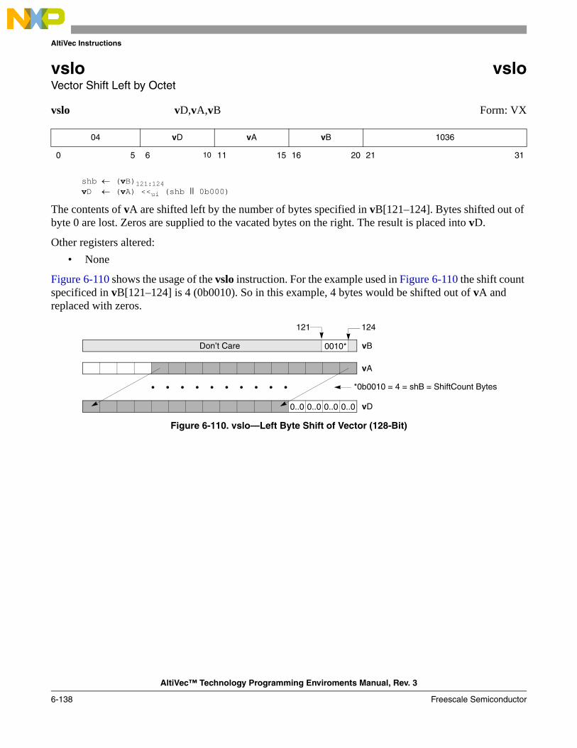
AltiVec Instructions
AltiVec™ Technology Programming Enviroments Manual, Rev. 3
6-138 Freescale Semiconductor
vslo vsloVector Shift Left by Octet
vslo vD,vA,vB Form: VX
shb ← (vB)121:124vD ← (vA) <<ui (shb || 0b000)
The contents of vA are shifted left by the number of bytes specified in vB[121–124]. Bytes shifted out of byte 0 are lost. Zeros are supplied to the vacated bytes on the right. The result is placed into vD.
Other registers altered:• None
Figure 6-110 shows the usage of the vslo instruction. For the example used in Figure 6-110 the shift count specificed in vB[121–124] is 4 (0b0010). So in this example, 4 bytes would be shifted out of vA and replaced with zeros.
Figure 6-110. vslo—Left Byte Shift of Vector (128-Bit)
04 vD vA vB 1036
0 5 6 10 11 15 16 20 21 31
vB
vA
vD
• • • • • • • • • • *0b0010 = 4 = shB = ShiftCount Bytes
Don’t Care
121 124
0..0
0010*
0..00..00..0

AltiVec Instructions
AltiVec™ Technology Programming Enviroments Manual, Rev. 3
Freescale Semiconductor 6-139
vslw vslwVector Shift Left Integer Word
vslw vD,vA,vB Form: VX
do i=0 to 127 by 32sh ← (vB)i+27:i+31vDi:i+31 ← (vA)i:i+31 <<ui sh
end
Each element is a word. Each element in vA is shifted left by the number of bits specified in the low-order 5 bits of the corresponding element in vB. Bits shifted out of bit 0 of the element are lost. Zeros are supplied to the vacated bits on the right. The result is placed into the corresponding element of vD.
Other registers altered:• None
Figure 6-111 shows the usage of the vslw instruction. Each of the four elements in the vectors, vA, vB, and vD, is 32 bits long. For the example used in Figure 6-111, the shift count specificed in the low-order 5 bits of the corresponding elements in vB is 6 (0b0010). In this example, 6 bits would be shifted out of each element in vA and replaced with zeros.
Figure 6-111. vslw—Shift Bits Left in Four Integer Elements (32-Bit)
04 vD vA vB 388
0 5 6 10 11 15 16 20 21 31
vA
vD
*0b00110 = 6 = sh = Shift count
sh
000000000000000000
zeros
000000
vB00110 00110 00110 00110*
9163 123 12759 953127

AltiVec Instructions
AltiVec™ Technology Programming Enviroments Manual, Rev. 3
6-140 Freescale Semiconductor
vspltb vspltbVector Splat Byte
vspltb vD,vB,UIMM Form: VX
b ← UIMM*8do i=0 to 127 by 8
vDi:i+7 ← (vB)b:b+7end
Each element of vspltb is a byte.
The contents of element UIMM in vB are replicated into each element of vD.
Other registers altered:• None
Programming Note: The vector splat instructions can be used in preparation for performing arithmetic for which one source vector is to consist of elements that all have the same value (for example, multiplying all elements of a vector register by a constant).
Figure 6-112 shows the usage of the vspltb instruction. Each of the sixteen elements in the vectors, vB and vD, is 8 bits long.
Figure 6-112. vspltb—Copy Contents to Sixteen Elements (8-Bit)
04 vD UIMM vB 524
0 5 6 10 11 15 16 20 21 31
vB
vD

AltiVec Instructions
AltiVec™ Technology Programming Enviroments Manual, Rev. 3
Freescale Semiconductor 6-141
vsplth vsplthVector Splat Half Word
vsplth vD,vB,UIMM Form: VX
b ← UIMM*16do i=0 to 127 by 16
vDi:i+15 ← (vB)b:b+15end
Each element of vsplth is a half word.
The contents of element UIMM in vB are replicated into each element of vD.
Other registers altered:• None
Programming Note: The vector splat instructions can be used in preparation for performing arithmetic for which one source vector is to consist of elements that all have the same value (for example, multiplying all elements of a vector register by a constant).
Figure 6-113 shows the usage of the vsplth instruction. Each of the eight elements in the vectors, vB and vD, is 16 bits long.
Figure 6-113. vsplth—Copy Contents to Eight Elements (16-Bit)
04 vD UIMM vB 588
0 5 6 10 11 15 16 20 21 31
vB
vD

AltiVec Instructions
AltiVec™ Technology Programming Enviroments Manual, Rev. 3
6-142 Freescale Semiconductor
vspltisb vspltisbVector Splat Immediate Signed Byte
vspltisb vD,SIMM Form: VX
do i=0 to 127 by 8vDi:i+7 ← SignExtend(SIMM,8)
end
Each element of vspltisb is a byte.
The value of the SIMM field, sign-extended to the length of the element, is replicated into each element of vD.
Other registers altered:• None
Figure 6-114 shows the usage of the vspltisb instruction. Each of the sixteen elements in the vector, vD, is 8 bits long.
Figure 6-114. vspltisb—Copy Value into Sixteen Signed Integer Elements (8-Bit)
04 vD SIMM 0000_0 780
0 5 6 10 11 15 16 20 21 31
SIMM
vD

AltiVec Instructions
AltiVec™ Technology Programming Enviroments Manual, Rev. 3
Freescale Semiconductor 6-143
vspltish vspltishVector Splat Immediate Signed Half Word
vspltish vD,SIMM Form: VX
do i=0 to 127 by 16vDi:i+15 ← SignExtend(SIMM,16)
end
Each element of vspltish is a half word.
The value of the SIMM field, sign-extended to the length of the element, is replicated into each element of vD.
Other registers altered:• None
Figure 6-115 shows the usage of the vspltish instruction. Each of the eight elements in vector, vD, is 16 bits long.
Figure 6-115. vspltish—Copy Value to Eight Signed Integer Elements (16-Bit)
04 vD SIMM 0000_0 844
0 5 6 10 11 15 16 20 21 31
SIMM
vD

AltiVec Instructions
AltiVec™ Technology Programming Enviroments Manual, Rev. 3
6-144 Freescale Semiconductor
vspltisw vspltiswVector Splat Immediate Signed Word
vspltisw vD,SIMM Form: VX
do i=0 to 127 by 32vDi:i+31 ← SignExtend(SIMM,32)
end
Each element of vspltisw is a word.
The value of the SIMM field, sign-extended to the length of the element, is replicated into each element of vD.
Other registers altered:• None
Figure 6-116 shows the usage of the vspltisw instruction. Each of the four elements in the vector, vD, is 32 bits long.
Figure 6-116. vspltisw—Copy Value to Four Signed Elements (32-Bit)
04 vD SIMM 0000_0 908
0 5 6 10 11 15 16 20 21 31
vD
SIMM

AltiVec Instructions
AltiVec™ Technology Programming Enviroments Manual, Rev. 3
Freescale Semiconductor 6-145
vspltw vspltwVector Splat Word
vspltw vD,vB,UIMM Form: VX
b ← UIMM*32do i=0 to 127 by 32
vDi:i+31 ← (vB)b:b+31end
Each element of vspltw is a word.
The contents of element UIMM in vB are replicated into each element of vD.
Other registers altered:• None
Programming Note: The Vector Splat instructions can be used in preparation for performing arithmetic for which one source vector is to consist of elements that all have the same value (for example, multiplying all elements of a Vector Register by a constant).
Figure 6-117 shows the usage of the vspltw instruction. Each of the four elements in the vector, vD, is 32 bits long.
Figure 6-117. vspltw—Copy Contents to Four Elements (32-Bit)
04 vD UIMM vB 652
0 5 6 10 11 15 16 20 21 31
vD
UIMM
AltiVec Instructions
AltiVec™ Technology Programming Enviroments Manual, Rev. 3
6-146 Freescale Semiconductor
vsr vsrVector Shift Right
vsr vD,vA,vB Form: VX
sh ← (vB)125:127t ← 1do i = 0 to 127 by 8
t ← t & ((vB)i+5:i+7 = sh)if t = 1 then vD ← (vA) >>ui shelse vD ← undefined
end
Let sh = vB[125–127]; sh is the shift count in bits (0≤sh≤7). The contents of vA are shifted right by sh bits. Bits shifted out of bit 127 are lost. Zeros are supplied to the vacated bits on the left. The result is placed into vD.
The contents of the low-order three bits of all byte elements in register vB must be identical to vB[125–127]; otherwise the value placed into register vD is undefined.
Other registers altered:• None
Programming Notes: A pair of vslo and vsl or vsro and vsr instructions, specifying the same shift count register, can be used to shift the contents of a vector register left or right by the number of bits (0–127) specified in the shift count register. The following example shifts the contents of vX left by the number of bits specified in vY and places the result into vZ.
vslo VZ,VX,VYvsl VZ,VZ,VY
A double-register shift by a dynamically specified number of bits (0–127) can be performed in six instructions. The following example shifts (vW) || (vX) left by the number of bits specified in vY and places the high-order 128 bits of the result into vZ.
vslo t1,VW,VY #shift high-order reg leftvsl t1,t1,VYvsububm t3,V0,VY #adjust shift count ((V0)=0)vsro t2,VX,t3 #shift low-order reg rightvsr t2,t2,t3vor VZ,t1,t2 #merge to get final result
04 vD vA vB 708
0 5 6 10 11 15 16 20 21 31

AltiVec Instructions
AltiVec™ Technology Programming Enviroments Manual, Rev. 3
Freescale Semiconductor 6-147
Figure 6-118 shows the usage of the vsr instruction. Each of the sixteen elements in the vectors, vA, vB, and vD, is 8 bits long. In the example in Figure 6-118 the shift count specificed in vB[125–127] is 7 (0b111), that shift count must then be put in the low-order three bits of all the byte elements in vB. In this example, the contents of vA are shifted right by 7 bits and replaced with zeros.
Figure 6-118. vsr—Shift Bits Right for Vectors (128-Bit)
vA
vD
• • • • • • • • • • *0b111 = 7 = sh = Shift Count
125 127
0...0
shzeros
vB111 111 111 111 111 111 111 111 111 111 111 111 111 111 111 111*

AltiVec Instructions
AltiVec™ Technology Programming Enviroments Manual, Rev. 3
6-148 Freescale Semiconductor
vsrab vsrabVector Shift Right Algebraic Byte
vsrab vD,vA,vB Form: VX
do i=0 to 127 by 8sh ← (vB)i+2:i+7vDi:i+7 ← (vA)i:i+7 >>si sh
end
Each element is a byte. Each element in vA is shifted right by the number of bits specified in the low-order 3 bits of the corresponding element in vB. Bits shifted out of bit n-1 of the element are lost. Bit 0 of each element in vA is replicated to fill the vacated bits on the left. The result is placed into the corresponding element of vD.
Other registers altered:• None
Figure 6-119 shows the usage of the vsrab instruction. Each of the sixteen elements in the vectors, vA and vD, is 8 bits long. In the example in Figure 6-119, the shift count specified is 7 (0b111) so this value is placed in each of the low-order three bits for all the byte elements in vB. In this example, 7 bits would be shifted out of each element in vA and replaced with bit 0 of each element in vA.
Figure 6-119. vsrab—Shift Bits Right in Sixteen Integer Elements (8-Bit)
04 vD vA vB 772
0 5 6 10 11 15 16 20 21 31
vA
vD
*0b111 = 7 = sh = Shift Count
x..x
sh
x..xx..xx..xx..xx..xx..xx..xx..xx..xx..xx..xx..xx..xx..xx..x
vB111 111 111 111 111 111 111 111 111 111 111 111 111 111 111 111*
*x = Bit 0 of each element in vA

AltiVec Instructions
AltiVec™ Technology Programming Enviroments Manual, Rev. 3
Freescale Semiconductor 6-149
vsrah vsrahVector Shift Right Algebraic Half Word
vsrah vD,vA,vB Form: VX
do i=0 to 127 by 16sh ← (vB)i+12:i+15vDi:i+15 ← (vA)i:i+15 >>si sh
end
Each element is a half word. Each element in vA is shifted right by the number of bits specified in the low-order 4 bits of the corresponding element in vB. Bits shifted out of bit 15 of the element are lost. Bit 0 of the element in vA is replicated to fill the vacated bits on the left. The result is placed into the corresponding element of vD.
Other registers altered:• None
Figure 6-120 shows the usage of the vsrah instruction. Each of the eight elements in the vectors, vA and vD, is 16 bits long. In the example in Figure 6-120, the shift count specified is 15 (0b1111) so this value is placed in each of the low-order four bits for all the half-word elements in vB. In this example, 15 bits would be shifted out of each element in vA and replaced with bit 0 of each element in vA.
Figure 6-120. vsrah—Shift Bits Right for Eight Integer Elements (16-Bit)
04 vD vA vB 836
0 5 6 10 11 15 16 20 21 31
1111 vB
vA
vD
*0b1111 = 15 = sh = Shift Count
x...x*
sh
x...xx...xx...xx...xx...xx...xx...x
*x = Bit 0 of each element in vA
1111 1111 1111 1111 1111 1111 1111*

AltiVec Instructions
AltiVec™ Technology Programming Enviroments Manual, Rev. 3
6-150 Freescale Semiconductor
vsraw vsrawVector Shift Right Algebraic Word
vsraw vD,vA,vB Form: VX
do i=0 to 127 by 32sh ← (vB)i+27:i+31vDi:i+31 ← (vA)i:i+31 >>si sh
end
Each element is a word. Each element in vA is shifted right by the number of bits specified in the low-order five bits of the corresponding element in vB. Bits shifted out of bit 31 of the element are lost. Bit 0 of each element in vA is replicated to fill the vacated bits on the left. The result is placed into the corresponding element of vD.
Other registers altered:• None
Figure 6-121 shows the usage of the vsraw instruction. Each of the four elements in the vectors, vA, vB, and vD, is 32 bits long. In the example in Figure 6-121, the shift count specified is 3 (0b00011) so this value is placed in each of the low-order five bits for all the byte elements in vB. In this example, 3 bits would be shifted out of each element in vA and replaced with bit 0 of each element in vA.
Figure 6-121. vsraw—Shift Bits Right in Four Integer Elements (32-Bit)
04 vD vA vB 900
0 5 6 10 11 15 16 20 21 31
000110001100011 vB
vA
vD
*00011 = 3 = sh = Shift Count
00011*
sh
x...xx...xx...x
*x = Bit 0 of each element in vA
x...x*

AltiVec Instructions
AltiVec™ Technology Programming Enviroments Manual, Rev. 3
Freescale Semiconductor 6-151
vsrb vsrbVector Shift Right Byte
vsrb vD,vA,vB Form: VX
do i=0 to 127 by 8sh ← (vB)i+5:i+7vDi:i+7 ← (vA)i:i+7 >>ui sh
end
Each element is a byte. Each element in vA is shifted right by the number of bits specified in the low-order 3 bits of the corresponding element in vB. Bits shifted out of bit 7 of the element are lost. Zeros are supplied to the vacated bits on the left. The result is placed into the corresponding element of vD.
Other registers altered:• None
Figure 6-122 shows the usage of the vsrb instruction. Each of the sixteen elements in the vectors, vA, vB, and vD, is 8 bits long. In the example in Figure 6-122 the shift count specified is 7 (0b111) so this value is placed in each of the low-order 3 bits for all the byte elements in vB. In this example, 7 bits would be shifted out of each element in vA and replaced with zeros.
Figure 6-122. vsrb—Shift Bits Right in Sixteen Integer Elements (8-Bit)
04 vD vA vB 516
0 5 6 10 11 15 16 20 21 31
vA
vD
*6 = sh = Shift Count
0..0
sh
0..00..00..00..00..00..00..00..00..00..00..00..00..00..00..0
zeros
vB111 111 111 111 111 111 111 111 111 111 111 111 111 111 111 111*

AltiVec Instructions
AltiVec™ Technology Programming Enviroments Manual, Rev. 3
6-152 Freescale Semiconductor
vsrh vsrhVector Shift Right Half Word
vsrh vD,vA,vB Form: VX
do i=0 to 127 by 16sh ← (vB)i+12:i+15vDi:i+15 ← (vA)i:i+15 >>ui sh
end
Each element is a half word. Each element in vA is shifted right by the number of bits specified in the low-order four bits of the corresponding element in vB. Bits shifted out of bit 15 of the element are lost. Zeros are supplied to the vacated bits on the left. The result is placed into the corresponding element of vD.
Other registers altered:• None
Figure 6-123 shows the usage of the vsrh instruction. Each of the eight elements in the vectors, vA, vB, and vD, is 16 bits long. In the example in Figure 6-123, the shift count specified is 15 (0b1111) so this value is placed in each of the low-order four bits for all the half-word elements in vB. In this example, 15 bits would be shifted out of each element in vA and replaced with zeros.
Figure 6-123. vsrh—Shift Bits Right for Eight Integer Elements (16-Bit)
04 vD vA vB 580
0 5 6 10 11 15 16 20 21 31
vA
vD
*0b1111 = 15 = sh = Shift Count
0...0
sh
0...00...00...00...00...00...00...0
zeros
1111 vB1111 1111 1111 1111 1111 1111 1111*

AltiVec Instructions
AltiVec™ Technology Programming Enviroments Manual, Rev. 3
Freescale Semiconductor 6-153
vsro vsroVector Shift Right Octet
vsro vD,vA,vB Form: VX
shb ← (vB)121:124vD ← (vA) >>ui (shb || 0b000)
The contents of vA are shifted right by the number of bytes specified in vB[121–124]. Bytes shifted out of vA are lost. Zeros are supplied to the vacated bytes on the left. The result is placed into vD.
Other registers altered:• None
Figure 6-124 shows the usage of the vsro instruction. Each of the sixteen elements in the vectors, vA and vD, is 8 bits long. In the example in Figure 6-124, the shift count specified is 5 (0b0101). In this example, 5 bytes would be shifted out of vA and replaced with zeros.
Figure 6-124. vsro—Vector Shift Right Octet
04 vD vA vB 1100
0 5 6 10 11 15 16 20 21 31
vB
vA
vD
• • • • • • • • • • *0b0101 = 5 = Shift Count
Don’t Care *0101
121 124
0..00..00..00..0 0..0

AltiVec Instructions
AltiVec™ Technology Programming Enviroments Manual, Rev. 3
6-154 Freescale Semiconductor
vsrw vsrwVector Shift Right Word
vsrw vD,vA,vB Form: VX
do i=0 to 127 by 32sh ← (vB)i+(27):i+31vDi:i+31 ← (vA)i:i+31 >>ui sh
end
Each element is a word. Each element in vA is shifted right by the number of bits specified in the low-order 5 bits of the corresponding element in vB. Bits shifted out of bit 31 of the element are lost. Zeros are supplied to the vacated bits on the left. The result is placed into the corresponding element of vD.
Other registers altered:• None
Figure 6-125 shows the usage of the vsrw instruction. Each of the four elements in the vectors, vA, vB, and vD, is 32 bits long.In the example in Figure 6-125 the shift count specified is 3 (0b00011) so this value is placed in each of the low-order five bits for all the byte elements in vB. In this example, 3 bits would be shifted out of each element in vA and replaced with zeros.
Figure 6-125. vsrw—Shift Bits Right in Four Integer Elements (32-Bit)
04 vD vA vB 644
0 5 6 10 11 15 16 20 21 31
vA
vD
*0b00011 = 3 = sh = Shift Count
sh
0...00...00...0
zeros
0...0
000110001100011 vB00011*

AltiVec Instructions
AltiVec™ Technology Programming Enviroments Manual, Rev. 3
Freescale Semiconductor 6-155
vsubcuw vsubcuwVector Subtract Carryout Unsigned Word
vsubcuw vD,vA,vB Form: VX
do i=0 to 127 by 32aop0:32 ← ZeroExtend((vA)i:i+31,33)bop0:32 ← ZeroExtend((vB)i:i+31,33)temp0:32 ← aop0:32 +int −bop0:32 +int 1vDi:i+31 ← ZeroExtend(temp0,32)
end
Each unsigned-integer word element in vB is subtracted from the corresponding unsigned-integer word element in vA. The complement of the borrow out of bit 0 of the 32-bit difference is zero-extended to 32 bits and placed into the corresponding word element of vD.
Other registers altered:• None
Figure 6-126 shows the usage of the vsubcuw instruction. Each of the four elements in the vectors, vA, vB, and vD, is 32 bits long.
g
Figure 6-126. vsubcuw—Subtract Carryout of Four Unsigned Integer Elements (32-Bit)
04 vD vA vB 1408
0 5 6 10 11 15 16 20 21 31
vB
vA
Zero-Ext
vD
- - - -

AltiVec Instructions
AltiVec™ Technology Programming Enviroments Manual, Rev. 3
6-156 Freescale Semiconductor
vsubfp vsubfpVector Subtract Floating-Point
vsubfp vD,vA,vB Form: VX
do i=0 to 127 by 32vDi:i+31 ← RndToNearFP32((vA)i:i+31 -fp (vB)i:i+31)
end
Each single-precision floating-point word element in vB is subtracted from the corresponding single-precision floating-point word element in vA. The result is rounded to the nearest single-precision floating-point number and placed into the corresponding word element of vD.
If VSCR[NJ]=1, every denormalized operand element is truncated to a 0 of the same sign before the operation is carried out, and each denormalized result element truncates to a 0 of the same sign.
Other registers altered:• None
Figure 6-127 shows the usage of the vsubfp instruction. Each of the four elements in the vectors, vA, vB, and vD, is 32 bits long.
Figure 6-127. vsubfp—Subtract Four Floating-Point Elements (32-Bit)
04 vD vA vB 74
0 5 6 10 11 15 16 20 21 31
-fp-fp-fp-fp
vA
vB
vD

AltiVec Instructions
AltiVec™ Technology Programming Enviroments Manual, Rev. 3
Freescale Semiconductor 6-157
vsubsbs vsubsbsVector Subtract Signed Byte Saturate
vsubsbs vD,vA,vB Form: VX
do i=0 to 127 by 8aop0:8 ← SignExtend((vA)i:i+7,9)bop0:8 ← SignExtend((vB)i:i+7,9)temp0:8 ← aop0:8 +int −bop0:8 +int 1vDi:i+7 ← SItoSIsat(temp0:8,8)
end
Each element is a byte. Each signed-integer element in vB is subtracted from the corresponding signed-integer element in vA.
If the intermediate result is greater than (27-1) it saturates to (27-1) and if it is less than -27 it saturates to -27, where 8 is the length of the element.
The signed-integer result is placed into the corresponding element of vD.
Other registers altered:• SAT
Figure 6-128 shows the usage of the vsubsbs instruction. Each of the sixteen elements in the vectors, vA, vB, and vD, is 8 bits long.
Figure 6-128. vsubsbs—Subtract Sixteen Signed Integer Elements (8-Bit)
04 vD vA vB 1792
0 5 6 10 11 15 16 20 21 31
- ---------------
vA
vB
vD

AltiVec Instructions
AltiVec™ Technology Programming Enviroments Manual, Rev. 3
6-158 Freescale Semiconductor
vsubshs vsubshsVector Subtract Signed Half Word Saturate
vsubshs vD,vA,vB Form: VX
do i=0 to 127 by 16aop0:16 ← SignExtend((vA)i:i+15,17)bop0:16 ← SignExtend((vB)i:i+15,17)temp0:16 ← aop0:16 +int -bop0:16 +int 1vDi:i+15 ← SItoSIsat(temp0:16,16)
end
Each element is a half word. Each signed-integer element in vB is subtracted from the corresponding signed-integer element in vA.
If the intermediate result is greater than (215-1) it saturates to (215-1) and if it is less than -215 it saturates to -215, where 16 is the length of the element.
The signed-integer result is placed into the corresponding element of vD.
Other registers altered:• SAT
Figure 6-129 shows the usage of the vsubshs instruction. Each of the eight elements in the vectors, vA, vB, and vD, is 16 bits long.
Figure 6-129. vsubshs—Subtract Eight Signed Integer Elements (16-Bit)
04 vD vA vB 1856
0 5 6 10 11 15 16 20 21 31
--------
vA
vB
vD

AltiVec Instructions
AltiVec™ Technology Programming Enviroments Manual, Rev. 3
Freescale Semiconductor 6-159
vsubsws vsubswsVector Subtract Signed Word Saturate
vsubsws vD,vA,vB Form: VX
do i=0 to 127 by 32aop0:32 ← SignExtend((vA)i:i+31,33)bop0:32 ← SignExtend((vB)i:i+31,33)temp0:32 ← aop0:32 +int −bop0:32 +int 1vDi:i+31 ← SItoSIsat(temp0:32,32)
end
Each element is a word. Each signed-integer element in vB is subtracted from the corresponding signed-integer element in vA.
If the intermediate result is greater than (231-1) it saturates to (231-1) and if it is less than -231 it saturates to -231, where 32 is the length of the element.
The signed-integer result is placed into the corresponding element of vD.
Other registers altered:• SAT
Figure 6-130 shows the usage of the vsubsws instruction. Each of the four elements in the vectors, vA, vB, and vD, is 32 bits long.
Figure 6-130. vsubsws—Subtract Four Signed Integer Elements (32-Bit)
04 vD vA vB 1920
0 5 6 10 11 15 16 20 21 31
----
vA
vB
vD

AltiVec Instructions
AltiVec™ Technology Programming Enviroments Manual, Rev. 3
6-160 Freescale Semiconductor
vsububm vsububmVector Subtract Byte Modulo
vsububm vD,vA,vB Form: VX
do i=0 to 127 by 8vDi:i+7 ← (vA)i:i+7 +int −(vB)i:i+7
end
Each element of vsububm is a byte.
Each integer element in vB is subtracted from the corresponding integer element in vA. The integer result is placed into the corresponding element of vD.
Other registers altered:• None
Note the vsububm instruction can be used for unsigned or signed integers.
Figure 6-131 shows the usage of the vsububm instruction. Each of the sixteen elements in the vectors, vA, vB, and vD, is 8 bits long.
Figure 6-131. vsububm—Subtract Sixteen Integer Elements (8-Bit)
04 vD vA vB 1024
0 5 6 10 11 15 16 20 21 31
- ---------------
vA
vB
vD

AltiVec Instructions
AltiVec™ Technology Programming Enviroments Manual, Rev. 3
Freescale Semiconductor 6-161
vsububs vsububsVector Subtract Unsigned Byte Saturate
vsububs vD,vA,vB Form: VX
do i=0 to 127 by 8aop0:8 ← ZeroExtend((vA)i:i+7,9)bop0:8 ← ZeroExtend((vB)i:i+7,9)temp0:8 ← aop0:8 +int −bop0:8 +int 1vDi:i+7 ← SItoUIsat(temp0:8,8)
end
Each element is a byte. Each unsigned-integer element in vB is subtracted from the corresponding unsigned-integer element in vA.
If the intermediate result is less than 0 it saturates to 0, where 8 is the length of the element. The unsigned-integer result is placed into the corresponding element of vD.
Other registers altered:• SAT
Figure 6-132 shows the usage of the vsububs instruction. Each of the sixteen elements in the vectors, vA, vB, and vD, is 8 bits long.
Figure 6-132. vsububs—Subtract Sixteen Unsigned Integer Elements (8-Bit)
04 vD vA vB 1536
0 5 6 10 11 15 16 20 21 31
- ---------------
vA
vB
vD

AltiVec Instructions
AltiVec™ Technology Programming Enviroments Manual, Rev. 3
6-162 Freescale Semiconductor
vsubuhm vsubuhmVector Subtract Half Word Modulo
vsubuhm vD,vA,vB Form: VX
do i=0 to 127 by 16vDi:i+15 ← (vA)i:i+15 +int −(vB)i:i+15
end
Each element is a half word. Each integer element in vB is subtracted from the corresponding integer element in vA. The integer result is placed into the corresponding element of vD.
Other registers altered:• None
Note the vsubuhm instruction can be used for unsigned or signed integers.
Figure 6-133 shows the usage of the vsubuhm instruction. Each of the eight elements in the vectors, vA, vB, and vD, is 16 bits long.
Figure 6-133. vsubuhm—Subtract Eight Integer Elements (16-Bit)
04 vD vA vB 1088
0 5 6 10 11 15 16 20 21 31
--------
vA
vB
vD

AltiVec Instructions
AltiVec™ Technology Programming Enviroments Manual, Rev. 3
Freescale Semiconductor 6-163
vsubuhs vsubuhsVector Subtract Unsigned Half Word Saturate
vsubuhs vD,vA,vB Form: VX
do i=0 to 127 by 16aop0:16 ← ZeroExtend((vA)i:i+15,17)bop0:16 ← ZeroExtend((vB)i:i+n:1,17)temp0:16 ← aop0:n +int −bop0:16 +int 1vDi:i+15 ← SItoUIsat(temp0:16,16)
end
Each element is a half word. Each unsigned-integer element in vB is subtracted from the corresponding unsigned-integer element in vA.
If the intermediate result is less than 0 it saturates to 0, where 16 is the length of the element. The unsigned-integer result is placed into the corresponding element of vD.
Other registers altered:• SAT
Figure 6-134 shows the usage of the vsubuhs instruction. Each of the eight elements in the vectors, vA, vB, and vD, is 16 bits long.
Figure 6-134. vsubuhs—Subtract Eight Unsigned Integer Elements (16-Bit)
04 vD vA vB 1600
0 5 6 10 11 15 16 20 21 31
--------
vA
vB
vD

AltiVec Instructions
AltiVec™ Technology Programming Enviroments Manual, Rev. 3
6-164 Freescale Semiconductor
vsubuwm vsubuwmVector Subtract Word Modulo
vsubuwm vD,vA,vB Form: VX
do i=0 to 127 by 32vDi:i+31 ← (vA)i:i+31 +int −(vB)i:i+31
end
Each element of vsubuwm is a word.
Each integer element in vB is subtracted from the corresponding integer element in vA. The integer result is placed into the corresponding element of vD.
Other registers altered:• None
Note the vsubuwm instruction can be used for unsigned or signed integers.
Figure 6-135 shows the usage of the vsubuwm instruction. Each of the four elements in the vectors, vA, vB, and vD, is 32 bits long.
Figure 6-135. vsubuwm—Subtract Four Integer Elements (32-Bit)
04 vD vA vB 1152
0 5 6 10 11 15 16 20 21 31
----
vA
vB
vD

AltiVec Instructions
AltiVec™ Technology Programming Enviroments Manual, Rev. 3
Freescale Semiconductor 6-165
vsubuws vsubuwsVector Subtract Unsigned Word Saturate
vsubuws vD,vA,vB Form: VX
do i=0 to 127 by 32aop0:32 ← ZeroExtend((vA)i:i+31,33)bop0:32 ← ZeroExtend((vB)i:i+31,33)temp0:32 ← aop0:32 +int −bop0:32 +int 1vDi:i+31 ← SItoUIsat(temp0:32,32)
end
Each element is a word. Each unsigned-integer element in vB is subtracted from the corresponding unsigned-integer element in vA.
If the intermediate result is less than 0 it saturates to 0, where 32 is the length of the element. The unsigned-integer result is placed into the corresponding element of vD.
Other registers altered:• SAT
Figure 6-136 shows the usage of the vsubuws instruction. Each of the four elements in the vectors, vA, vB, and vD, is 32 bits long.
Figure 6-136. vsubuws—Subtract Four Signed Integer Elements (32-Bit)
04 vD vA vB 1664
0 5 6 10 11 15 16 20 21 31
----
vA
vB
vD

AltiVec Instructions
AltiVec™ Technology Programming Enviroments Manual, Rev. 3
6-166 Freescale Semiconductor
vsumsws vsumswsVector Sum Across Signed Word Saturate
vsumsws vD,vA,vB Form: VX
temp0:34 ← SignExtend((vB)96:127,35)do i=0 to 127 by 32
temp0:34 ← temp0:34 +int SignExtend((vA)i:i+31,35)vD ← 960 || SItoSIsat(temp0:34,32)
end
The signed-integer sum of the four signed-integer word elements in vA is added to the signed-integer word element in bits of vB[96–127]. If the intermediate result is greater than (231-1) it saturates to (231-1) and if it is less than -231 it saturates to -231. The signed-integer result is placed into bits vD[96–127]. Bits vD[0–95] are cleared.
Other registers altered:• SAT
Figure 6-137 shows the usage of the vsumsws instruction. Each of the four elements in the vectors, vA, vB, and vD, is 32 bits long.
Figure 6-137. vsumsws—Sum Four Signed Integer Elements (32-Bit)
04 vD vA vB 1928
0 5 6 10 11 15 16 20 21 31
+
vA
vB
vD
0 31 32
95
63 64 95 96 127
0 96 127

AltiVec Instructions
AltiVec™ Technology Programming Enviroments Manual, Rev. 3
Freescale Semiconductor 6-167
vsum2sws vsum2swsVector Sum Across Partial (1/2) Signed Word Saturate
vsum2sws vD,vA,vB Form: VX
do i=0 to 127 by 64temp0:33 ← SignExtend((vB)i+32:i+63,34)do j=0 to 63 by 32
temp0:33 ← temp0:33 +int SignExtend((vA)i+j:i+j+31,34)endvDi:i+63 ← 320 || SItoSIsat(temp0:33,32)
end
The signed-integer sum of the first two signed-integer word elements in register vA is added to the signed-integer word element in vB[32–63]. If the intermediate result is greater than (231-1) it saturates to (231-1) and if it is less than -231 it saturates to -231. The signed-integer result is placed into vD[32–63]. The signed-integer sum of the last two signed-integer word elements in register vA is added to the signed-integer word element in vB[96–127]. If the intermediate result is greater than (231-1) it saturates to (231-1) and if it is less than -231 it saturates to -231. The signed-integer result is placed into vD[96–127]. The register vD[0–31,64–95] are cleared to 0.
Other registers altered:• SAT
Figure 6-138 shows the usage of the vsum2sws instruction. Each of the four elements in the vectors, vA, vB, and vD, is 32 bits long.
Figure 6-138. vsum2sws—Two Sums in the Four Signed Integer Elements (32-Bit)
04 vD vA vB 1672
0 5 6 10 11 15 16 20 21 31
+
vA
vB
vD0 0 0 0 0 0 0 00 0 0 0 0 0 0 0
+

AltiVec Instructions
AltiVec™ Technology Programming Enviroments Manual, Rev. 3
6-168 Freescale Semiconductor
vsum4sbs vsum4sbsVector Sum Across Partial (1/4) Signed Byte Saturate
vsum4sbs vD,vA,vB Form: VX
do i=0 to 127 by 32temp0:32 ← SignExtend((vB)i:i+31,33) do j=0 to 31 by 8
temp0:32 ← temp0:32 +int SignExtend((vA)i+j:i+j+7,33)endvDi:i+31 ← SItoSIsat(temp0:32,32)
end
For each word element in vB the following operations are performed in the order shown.• The signed-integer sum of the four signed-integer byte elements contained in the corresponding
word element of register vA is added to the signed-integer word element in register vB.• If the intermediate result is greater than (231-1) it saturates to (231-1) and if it is less than -231 it
saturates to -231.• The signed-integer result is placed into the corresponding word element of vD.
Other registers altered:• SAT
Figure 6-139 shows the usage of the vsum4sbs instruction. Each of the sixteen elements in the vector, vA, is 8 bits long. Each of the four elements in the vectors, vB and vD, is 32 bits long.
Figure 6-139. vsum4sbs—Sum of Four Signed Integer Byte Elements with a Word Element (32-Bit)
04 vD vA vB 1800
0 5 6 10 11 15 16 20 21 31
vA
vB
vD
++++

AltiVec Instructions
AltiVec™ Technology Programming Enviroments Manual, Rev. 3
Freescale Semiconductor 6-169
vsum4shs vsum4shsVector Sum Across Partial (1/4) Signed Half Word Saturate
vsum4shs vD,vA,vB Form: VX
do i=0 to 127 by 32temp0:32 ← SignExtend((vB)i:i+31,33)do j=0 to 31 by 16
temp0:32 ← temp0:32 +int SignExtend((vA)i+j:i+j+15,33)end
vDi:i+31 ← SItoSIsat(temp0:32,32)end
For each word element in register vB the following operations are performed, in the order shown.• The signed-integer sum of the two signed-integer half-word elements contained in the
corresponding word element of register vA is added to the signed-integer word element in vB.• If the intermediate result is greater than (231-1) it saturates to (231-1) and if it is less than -231 it
saturates to -231.• The signed-integer result is placed into the corresponding word element of vD.
Other registers altered:• SAT
Figure 6-140 shows the usage of the vsum4shs instruction. Each of the eight elements in the vector, vA, is 16 bits long. Each of the four elements in the vectors, vB and vD, is 32 bits long.
Figure 6-140. vsum4shs—Sum of Two Signed Integer Half-Word Elements with a Word Element (32-Bit)
04 vD vA vB 1608
0 5 6 10 11 15 16 20 21 31
vA
vB
vD
++++
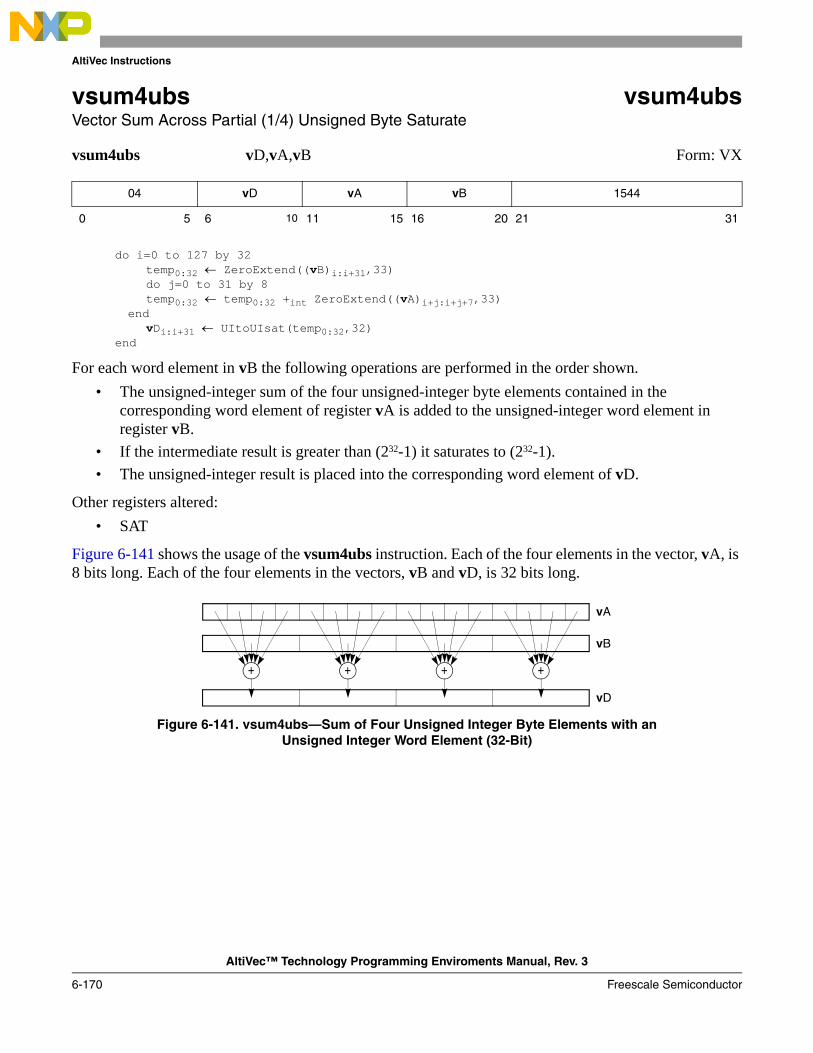
AltiVec Instructions
AltiVec™ Technology Programming Enviroments Manual, Rev. 3
6-170 Freescale Semiconductor
vsum4ubs vsum4ubsVector Sum Across Partial (1/4) Unsigned Byte Saturate
vsum4ubs vD,vA,vB Form: VX
do i=0 to 127 by 32temp0:32 ← ZeroExtend((vB)i:i+31,33)do j=0 to 31 by 8temp0:32 ← temp0:32 +int ZeroExtend((vA)i+j:i+j+7,33)
endvDi:i+31 ← UItoUIsat(temp0:32,32)
end
For each word element in vB the following operations are performed in the order shown.• The unsigned-integer sum of the four unsigned-integer byte elements contained in the
corresponding word element of register vA is added to the unsigned-integer word element in register vB.
• If the intermediate result is greater than (232-1) it saturates to (232-1).• The unsigned-integer result is placed into the corresponding word element of vD.
Other registers altered:• SAT
Figure 6-141 shows the usage of the vsum4ubs instruction. Each of the four elements in the vector, vA, is 8 bits long. Each of the four elements in the vectors, vB and vD, is 32 bits long.
Figure 6-141. vsum4ubs—Sum of Four Unsigned Integer Byte Elements with an Unsigned Integer Word Element (32-Bit)
04 vD vA vB 1544
0 5 6 10 11 15 16 20 21 31
vA
vB
vD
++++
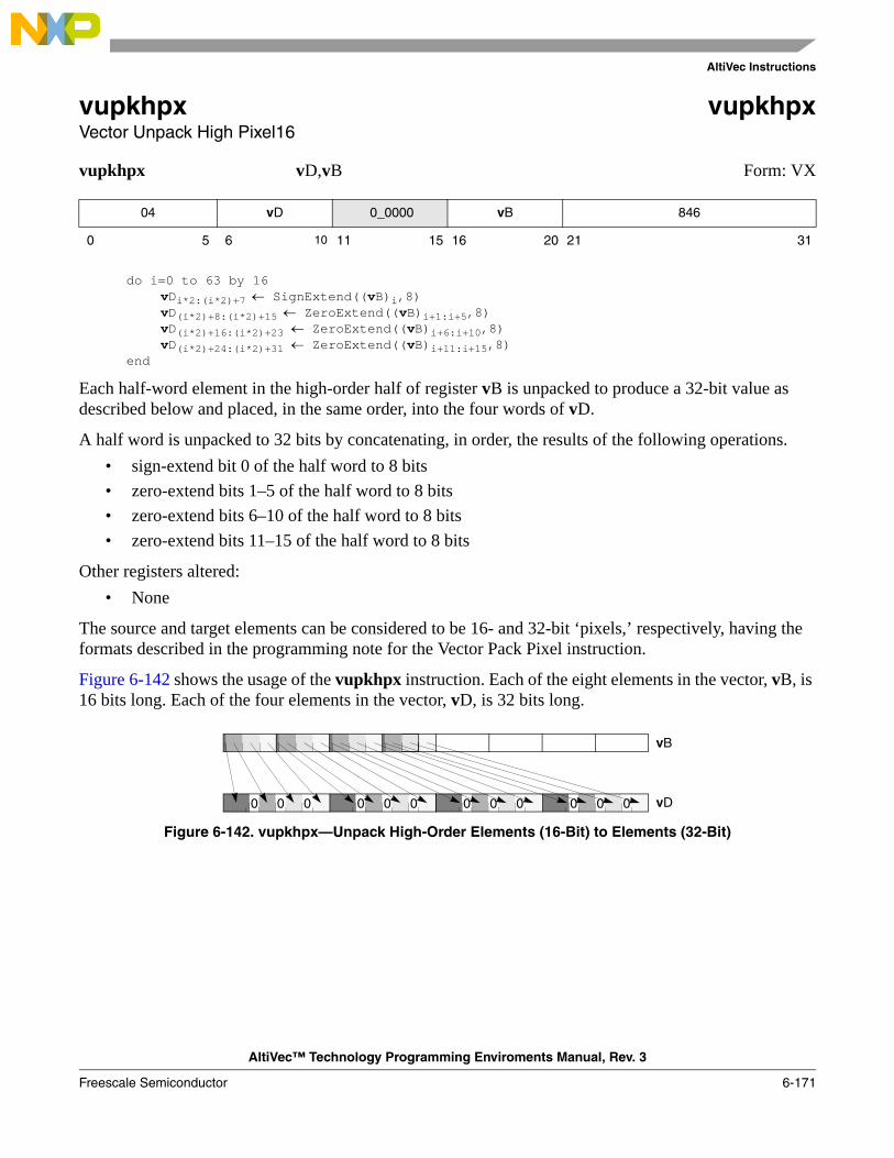
AltiVec Instructions
AltiVec™ Technology Programming Enviroments Manual, Rev. 3
Freescale Semiconductor 6-171
vupkhpx vupkhpxVector Unpack High Pixel16
vupkhpx vD,vB Form: VX
do i=0 to 63 by 16vDi*2:(i*2)+7 ← SignExtend((vB)i,8)vD(i*2)+8:(i*2)+15 ← ZeroExtend((vB)i+1:i+5,8)vD(i*2)+16:(i*2)+23 ← ZeroExtend((vB)i+6:i+10,8)vD(i*2)+24:(i*2)+31 ← ZeroExtend((vB)i+11:i+15,8)
end
Each half-word element in the high-order half of register vB is unpacked to produce a 32-bit value as described below and placed, in the same order, into the four words of vD.
A half word is unpacked to 32 bits by concatenating, in order, the results of the following operations.• sign-extend bit 0 of the half word to 8 bits• zero-extend bits 1–5 of the half word to 8 bits• zero-extend bits 6–10 of the half word to 8 bits• zero-extend bits 11–15 of the half word to 8 bits
Other registers altered:• None
The source and target elements can be considered to be 16- and 32-bit ‘pixels,’ respectively, having the formats described in the programming note for the Vector Pack Pixel instruction.
Figure 6-142 shows the usage of the vupkhpx instruction. Each of the eight elements in the vector, vB, is 16 bits long. Each of the four elements in the vector, vD, is 32 bits long.
Figure 6-142. vupkhpx—Unpack High-Order Elements (16-Bit) to Elements (32-Bit)
04 vD 0_0000 vB 846
0 5 6 10 11 15 16 20 21 31
vB
vD000 000 000 000
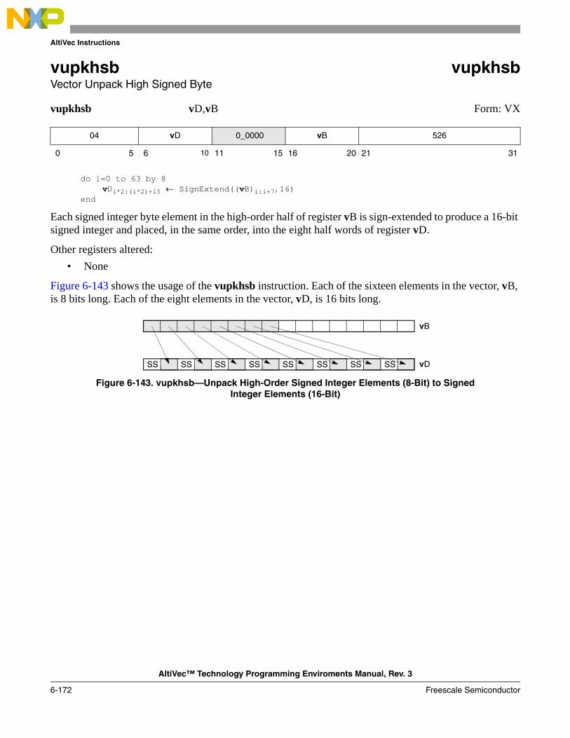
AltiVec Instructions
AltiVec™ Technology Programming Enviroments Manual, Rev. 3
6-172 Freescale Semiconductor
vupkhsb vupkhsbVector Unpack High Signed Byte
vupkhsb vD,vB Form: VX
do i=0 to 63 by 8vDi*2:(i*2)+15 ← SignExtend((vB)i:i+7,16)
end
Each signed integer byte element in the high-order half of register vB is sign-extended to produce a 16-bit signed integer and placed, in the same order, into the eight half words of register vD.
Other registers altered:• None
Figure 6-143 shows the usage of the vupkhsb instruction. Each of the sixteen elements in the vector, vB, is 8 bits long. Each of the eight elements in the vector, vD, is 16 bits long.
Figure 6-143. vupkhsb—Unpack High-Order Signed Integer Elements (8-Bit) to Signed Integer Elements (16-Bit)
04 vD 0_0000 vB 526
0 5 6 10 11 15 16 20 21 31
SSSSSSSSSSSSSSSS
vB
vD
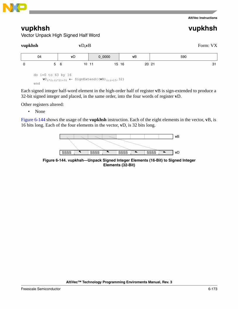
AltiVec Instructions
AltiVec™ Technology Programming Enviroments Manual, Rev. 3
Freescale Semiconductor 6-173
vupkhsh vupkhshVector Unpack High Signed Half Word
vupkhsh vD,vB Form: VX
do i=0 to 63 by 16vDi*2:(i*2)+31 ← SignExtend((vB)i:i+15,32)
end
Each signed integer half-word element in the high-order half of register vB is sign-extended to produce a 32-bit signed integer and placed, in the same order, into the four words of register vD.
Other registers altered:• None
Figure 6-144 shows the usage of the vupkhsh instruction. Each of the eight elements in the vector, vB, is 16 bits long. Each of the four elements in the vector, vD, is 32 bits long.
Figure 6-144. vupkhsh—Unpack Signed Integer Elements (16-Bit) to Signed Integer Elements (32-Bit)
04 vD 0_0000 vB 590
0 5 6 10 11 15 16 20 21 31
vB
vDSSSSSSSSSSSSSSSS

AltiVec Instructions
AltiVec™ Technology Programming Enviroments Manual, Rev. 3
6-174 Freescale Semiconductor
vupklpx vupklpxVector Unpack Low Pixel16
vupklpx vD,vB Form: VX
do i=0 to 63 by 16vDi*2:(i*2)+7 ← SignExtend((vB)i+64,8)vD(i*2)+8:(i*2)+15 ← ZeroExtend((vB)i+65:i+69,8)vD(i*2)+16:(i*2)+23 ← ZeroExtend((vB)i+70:i+74,8)vD(i*2)+24:(i*2)+31 ← ZeroExtend((vB)i+75:i+79,8)
end
Each half-word element in the low-order half of register vB is unpacked to produce a 32-bit value as described below and placed, in the same order, into the four words of register vD.
A half word is unpacked to 32 bits by concatenating, in order, the results of the following operations.• sign-extend bit 0 of the half word to 8 bits• zero-extend bits 1–5 of the half word to 8 bits• zero-extend bits 6–10 of the half word to 8 bits• zero-extend bits 11–15 of the half word to 8 bits
Other registers altered:• None
Programming note: Notice that the unpacking done by the Vector Unpack Pixel instructions does not reverse the packing done by the Vector Pack Pixel instruction. Specifically, if a 16-bit pixel is unpacked to a 32-bit pixel which is then packed to a 16-bit pixel, the resulting 16-bit pixel will not, in general, be equal to the original 16-bit pixel (because, for each channel except the first, Vector Unpack Pixel inserts high-order bits while Vector Pack Pixel discards low-order bits).
Figure 6-145 shows the usage of the vupklpx instruction. Each of the eight elements in the vector, vB, is 16 bits long. Each of the four elements in the vector, vD, is 32 bits long.
Figure 6-145. vupklpx—Unpack Low-Order Elements (16-Bit) to Elements (32-Bit)
04 vD 0_0000 vB 974
0 5 6 10 11 15 16 20 21 31
vB
vD000000000 000000
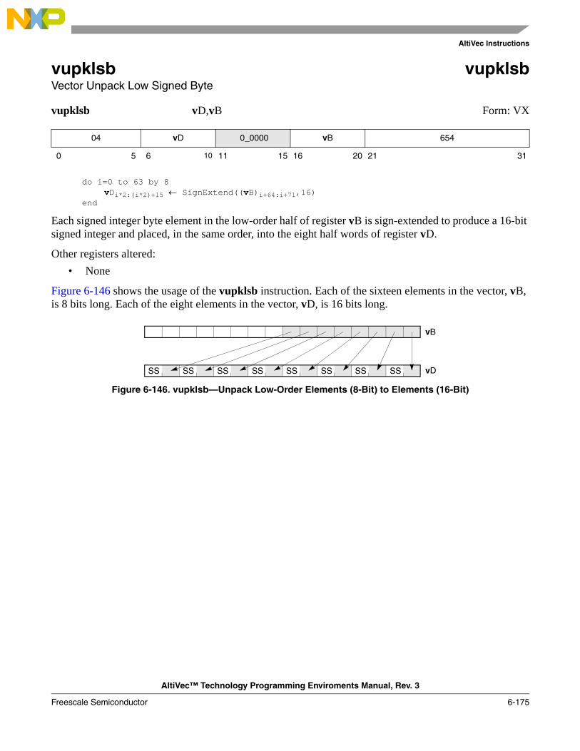
AltiVec Instructions
AltiVec™ Technology Programming Enviroments Manual, Rev. 3
Freescale Semiconductor 6-175
vupklsb vupklsbVector Unpack Low Signed Byte
vupklsb vD,vB Form: VX
do i=0 to 63 by 8vDi*2:(i*2)+15 ← SignExtend((vB)i+64:i+71,16)
end
Each signed integer byte element in the low-order half of register vB is sign-extended to produce a 16-bit signed integer and placed, in the same order, into the eight half words of register vD.
Other registers altered:• None
Figure 6-146 shows the usage of the vupklsb instruction. Each of the sixteen elements in the vector, vB, is 8 bits long. Each of the eight elements in the vector, vD, is 16 bits long.
Figure 6-146. vupklsb—Unpack Low-Order Elements (8-Bit) to Elements (16-Bit)
04 vD 0_0000 vB 654
0 5 6 10 11 15 16 20 21 31
vB
vDSSSSSSSSSSSSSSSS

AltiVec Instructions
AltiVec™ Technology Programming Enviroments Manual, Rev. 3
6-176 Freescale Semiconductor
vupklsh vupklshVector Unpack Low Signed Half Word
vupklsh vD,vB Form: VX
do i=0 to 63 by 16vDi*2:(i*2)+31 ← SignExtend((vB)i+64:i+79,32)
end
Each signed integer half word element in the low-order half of register vB is sign-extended to produce a 32-bit signed integer and placed, in the same order, into the four words of register vD.
Other registers altered:• None
Figure 6-147 shows the usage of the vupklsh instruction. Each of the eight elements in the vector, vB, is 16 bits long. Each of the four elements in the vector, vD, is 32 bits long.
Figure 6-147. vupklsh—Unpack Low-Order Signed Integer Elements (16-Bit) to Signed Integer Elements (32-Bit)
04 vD 0_0000 vB 718
0 5 6 10 11 15 16 20 21 31
vB
vDSSSSSSSSSSSSSSSS
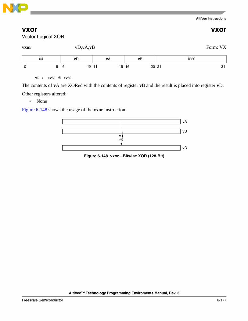
AltiVec Instructions
AltiVec™ Technology Programming Enviroments Manual, Rev. 3
Freescale Semiconductor 6-177
vxor vxorVector Logical XOR
vxor vD,vA,vB Form: VX
vD ← (vA) ⊕ (vB)
The contents of vA are XORed with the contents of register vB and the result is placed into register vD.
Other registers altered:• None
Figure 6-148 shows the usage of the vxor instruction.
Figure 6-148. vxor—Bitwise XOR (128-Bit)
04 vD vA vB 1220
0 5 6 10 11 15 16 20 21 31
⊕
vA
vB
vD

AltiVec Instructions
AltiVec™ Technology Programming Enviroments Manual, Rev. 3
6-178 Freescale Semiconductor

AltiVec™ Technology Programming Enviroments Manual, Rev. 3
Freescale Semiconductor A-1
Appendix A AltiVec Instruction Set ListingsThis appendix lists the instruction set for AltiVec technology. Instructions are sorted by mnemonic, opcode, and form. Also included in this appendix is a quick reference table that contains general information, such as the architecture level, privilege level, and form, and indicates if the instruction is optional.
Note that split fields, which represent the concatenation of sequences from left to right, are shown in lower case.
The following key applies to the tables in this appendix.
A.1 Instructions Sorted by Mnemonic in Decimal FormatTable A-1 lists the instructions implemented in the AltiVec architecture in alphabetical order by mnemonic. The primary and extended opcodes are decimal numbers.
Table A-1. Instructions Sorted by Mnemonic in Decimal Format
Name 0 5 6 7 8 9 10 11 12 13 14 15 16 17 18 19 20 21 22 23 24 25 26 27 28 29 30 31
dss 31 0 0_0 STRM 0_0000 0000_0 822 0
dssall 31 1 0_0 STRM 0_0000 0000_0 822 0
dst 31 0 0_0 STRM A B 342 0
dstst 31 0 0_0 STRM A B 374 0
dststt 31 1 0_0 STRM A B 374 0
dstt 31 1 0_0 STRM A B 342 0
lvebx 31 vD A B 7 0
lvehx 31 vD A B 39 0
lvewx 31 vD A B 71 0
lvsl 31 vD A B 6 0
lvsr 31 vD A B 38 0
lvx 31 vD A B 103 0
lvxl 31 vD A B 359 0
mfvscr 04 vD 0_0000 0000_0 1540
mtvscr 04 00_000 0_0000 vB 1604
stvebx 31 vS A B 135 0
stvehx 31 vS A B 167 0
Reserved BitsKey:

AltiVec Instruction Set Listings
AltiVec™ Technology Programming Enviroments Manual, Rev. 3
A-2 Freescale Semiconductor
stvewx 31 vS A B 199 0
stvx 31 vS A B 231 0
stvxl 31 vS A B 487 0
vaddcuw 04 vD vA vB 384
vaddfp 04 vD vA vB 10
vaddsbs 04 vD vA vB 768
vaddshs 04 vD vA vB 832
vaddsws 04 vD vA vB 896
vaddubm 04 vD vA vB 0
vaddubs 04 vD vA vB 512
vadduhm 04 vD vA vB 64
vadduhs 04 vD vA vB 576
vadduwm 04 vD vA vB 128
vadduws 04 vD vA vB 640
vand 04 vD vA vB 1028
vandc 04 vD vA vB 1092
vavgsb 04 vD vA vB 1282
vavgsh 04 vD vA vB 1346
vavgsw 04 vD vA vB 1410
vavgub 04 vD vA vB 1026
vavguh 04 vD vA vB 1090
vavguw 04 vD vA vB 1154
vcfsx 04 vD UIMM vB 842
vcfux 04 vD UIMM vB 778
vcmpbfpx 04 vD vA vB Rc 966
vcmpeqfpx 04 vD vA vB Rc 198
vcmpequbx 04 vD vA vB Rc 6
vcmpequhx 04 vD vA vB Rc 70
vcmpequwx 04 vD vA vB Rc 134
vcmpgefpx 04 vD vA vB Rc 454
vcmpgtfpx 04 vD vA vB Rc 710
vcmpgtsbx 04 vD vA vB Rc 774
vcmpgtshx 04 vD vA vB Rc 838
vcmpgtswx 04 vD vA vB Rc 902
vcmpgtubx 04 vD vA vB Rc 518
vcmpgtuhx 04 vD vA vB Rc 582
vcmpgtuwx 04 vD vA vB Rc 646
Table A-1. Instructions Sorted by Mnemonic in Decimal Format (continued)
Name 0 5 6 7 8 9 10 11 12 13 14 15 16 17 18 19 20 21 22 23 24 25 26 27 28 29 30 31

AltiVec Instruction Set Listings
AltiVec™ Technology Programming Enviroments Manual, Rev. 3
Freescale Semiconductor A-3
vctsxs 04 vD UIMM vB 970
vctuxs 04 vD UIMM vB 906
vexptefp 04 vD 0_0000 vB 394
vlogefp 04 vD 0_0000 vB 458
vmaddfp 04 vD vA vB vC 46
vmaxfp 04 vD vA vB 1034
vmaxsb 04 vD vA vB 258
vmaxsh 04 vD vA vB 322
vmaxsw 04 vD vA vB 386
vmaxub 04 vD vA vB 2
vmaxuh 04 vD vA vB 66
vmaxuw 04 vD vA vB 130
vmhaddshs 04 vD vA vB vC 32
vmhraddshs 04 vD vA vB vC 33
vminfp 04 vD vA vB 1098
vminsb 04 vD vA vB 770
vminsh 04 vD vA vB 834
vminsw 04 vD vA vB 898
vminub 04 vD vA vB 514
vminuh 04 vD vA vB 578
vminuw 04 vD vA vB 642
vmladduhm 04 vD vA vB vC 34
vmrghb 04 vD vA vB 12
vmrghh 04 vD vA vB 76
vmrghw 04 vD vA vB 140
vmrglb 04 vD vA vB 268
vmrglh 04 vD vA vB 332
vmrglw 04 vD vA vB 396
vmsummbm 04 vD vA vB vC 37
vmsumshm 04 vD vA vB vC 40
vmsumshs 04 vD vA vB vC 41
vmsumubm 04 vD vA vB vC 36
vmsumuhm 04 vD vA vB vC 38
vmsumuhs 04 vD vA vB vC 39
vmulesb 04 vD vA vB 776
vmulesh 04 vD vA vB 840
vmuleub 04 vD vA vB 520
Table A-1. Instructions Sorted by Mnemonic in Decimal Format (continued)
Name 0 5 6 7 8 9 10 11 12 13 14 15 16 17 18 19 20 21 22 23 24 25 26 27 28 29 30 31

AltiVec Instruction Set Listings
AltiVec™ Technology Programming Enviroments Manual, Rev. 3
A-4 Freescale Semiconductor
vmuleuh 04 vD vA vB 584
vmulosb 04 vD vA vB 264
vmulosh 04 vD vA vB 328
vmuloub 04 vD vA vB 8
vmulouh 04 vD vA vB 72
vnmsubfp 04 vD vA vB vC 47
vnor 04 vD vA vB 1284
vor 04 vD vA vB 1156
vperm 04 vD vA vB vC 43
vpkpx 04 vD vA vB 782
vpkshss 04 vD vA vB 398
vpkshus 04 vD vA vB 270
vpkswss 04 vD vA vB 462
vpkswus 04 vD vA vB 334
vpkuhum 04 vD vA vB 14
vpkuhus 04 vD vA vB 142
vpkuwum 04 vD vA vB 78
vpkuwus 04 vD vA vB 206
vrefp 04 vD 0_0000 vB 266
vrfim 04 vD 0_0000 vB 714
vrfin 04 vD 0_0000 vB 522
vrfip 04 vD 0_0000 vB 650
vrfiz 04 vD 0_0000 vB 586
vrlb 04 vD vA vB 4
vrlh 04 vD vA vB 68
vrlw 04 vD vA vB 132
vrsqrtefp 04 vD 0_0000 vB 330
vsel 04 vD vA vB vC 42
vsl 04 vD vA vB 452
vslb 04 vD vA vB 260
vsldoi 04 vD vA vB 0 SH 44
vslh 04 vD vA vB 324
vslo 04 vD vA vB 1036
vslw 04 vD vA vB 388
vspltb 04 vD UIMM vB 524
vsplth 04 vD UIMM vB 588
vspltisb 04 vD SIMM 0000_0 780
Table A-1. Instructions Sorted by Mnemonic in Decimal Format (continued)
Name 0 5 6 7 8 9 10 11 12 13 14 15 16 17 18 19 20 21 22 23 24 25 26 27 28 29 30 31

AltiVec Instruction Set Listings
AltiVec™ Technology Programming Enviroments Manual, Rev. 3
Freescale Semiconductor A-5
vspltish 04 vD SIMM 0000_0 844
vspltisw 04 vD SIMM 0000_0 908
vspltw 04 vD UIMM vB 652
vsr 04 vD vA vB 708
vsrab 04 vD vA vB 772
vsrah 04 vD vA vB 836
vsraw 04 vD vA vB 900
vsrb 04 vD vA vB 516
vsrh 04 vD vA vB 580
vsro 04 vD vA vB 1100
vsrw 04 vD vA vB 644
vsubcuw 04 vD vA vB 1408
vsubfp 04 vD vA vB 74
vsubsbs 04 vD vA vB 1792
vsubshs 04 vD vA vB 1856
vsubsws 04 vD vA vB 1920
vsububm 04 vD vA vB 1024
vsububs 04 vD vA vB 1536
vsubuhm 04 vD vA vB 1088
vsubuhs 04 vD vA vB 1600
vsubuwm 04 vD vA vB 1152
vsubuws 04 vD vA vB 1664
vsumsws 04 vD vA vB 1928
vsum2sws 04 vD vA vB 1672
vsum4sbs 04 vD vA vB 1800
vsum4shs 04 vD vA vB 1608
vsum4ubs 04 vD vA vB 1544
vupkhpx 04 vD 0_0000 vB 846
vupkhsb 04 vD 0_0000 vB 526
vupkhsh 04 vD 0_0000 vB 590
vupklpx 04 vD 0_0000 vB 974
vupklsb 04 vD 0_0000 vB 654
vupklsh 04 vD 0_0000 vB 718
vxor 04 vD vA vB 1220
Table A-1. Instructions Sorted by Mnemonic in Decimal Format (continued)
Name 0 5 6 7 8 9 10 11 12 13 14 15 16 17 18 19 20 21 22 23 24 25 26 27 28 29 30 31
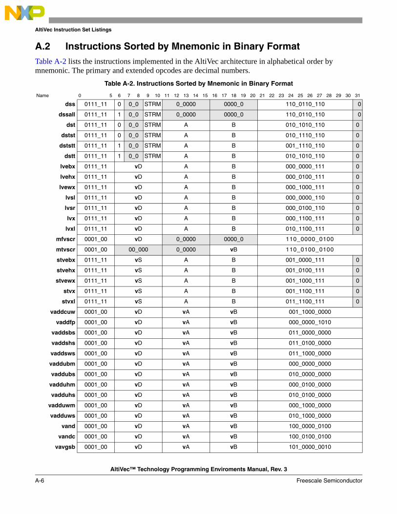
AltiVec Instruction Set Listings
AltiVec™ Technology Programming Enviroments Manual, Rev. 3
A-6 Freescale Semiconductor
A.2 Instructions Sorted by Mnemonic in Binary FormatTable A-2 lists the instructions implemented in the AltiVec architecture in alphabetical order by mnemonic. The primary and extended opcodes are decimal numbers.
Table A-2. Instructions Sorted by Mnemonic in Binary Format
Name 0 5 6 7 8 9 10 11 12 13 14 15 16 17 18 19 20 21 22 23 24 25 26 27 28 29 30 31
dss 0111_11 0 0_0 STRM 0_0000 0000_0 110_0110_110 0
dssall 0111_11 1 0_0 STRM 0_0000 0000_0 110_0110_110 0
dst 0111_11 0 0_0 STRM A B 010_1010_110 0
dstst 0111_11 0 0_0 STRM A B 010_1110_110 0
dststt 0111_11 1 0_0 STRM A B 001_1110_110 0
dstt 0111_11 1 0_0 STRM A B 010_1010_110 0
lvebx 0111_11 vD A B 000_0000_111 0
lvehx 0111_11 vD A B 000_0100_111 0
lvewx 0111_11 vD A B 000_1000_111 0
lvsl 0111_11 vD A B 000_0000_110 0
lvsr 0111_11 vD A B 000_0100_110 0
lvx 0111_11 vD A B 000_1100_111 0
lvxl 0111_11 vD A B 010_1100_111 0
mfvscr 0001_00 vD 0_0000 0000_0 110_0000_0100
mtvscr 0001_00 00_000 0_0000 vB 110_0100_0100
stvebx 0111_11 vS A B 001_0000_111 0
stvehx 0111_11 vS A B 001_0100_111 0
stvewx 0111_11 vS A B 001_1000_111 0
stvx 0111_11 vS A B 001_1100_111 0
stvxl 0111_11 vS A B 011_1100_111 0
vaddcuw 0001_00 vD vA vB 001_1000_0000
vaddfp 0001_00 vD vA vB 000_0000_1010
vaddsbs 0001_00 vD vA vB 011_0000_0000
vaddshs 0001_00 vD vA vB 011_0100_0000
vaddsws 0001_00 vD vA vB 011_1000_0000
vaddubm 0001_00 vD vA vB 000_0000_0000
vaddubs 0001_00 vD vA vB 010_0000_0000
vadduhm 0001_00 vD vA vB 000_0100_0000
vadduhs 0001_00 vD vA vB 010_0100_0000
vadduwm 0001_00 vD vA vB 000_1000_0000
vadduws 0001_00 vD vA vB 010_1000_0000
vand 0001_00 vD vA vB 100_0000_0100
vandc 0001_00 vD vA vB 100_0100_0100
vavgsb 0001_00 vD vA vB 101_0000_0010

AltiVec Instruction Set Listings
AltiVec™ Technology Programming Enviroments Manual, Rev. 3
Freescale Semiconductor A-7
vavgsh 0001_00 vD vA vB 101_0100_0010
vavgsw 0001_00 vD vA vB 101_1000_0010
vavgub 0001_00 vD vA vB 100_0000_0010
vavguh 0001_00 vD vA vB 100_0100_0010
vavguw 0001_00 vD vA vB 100_1000_0010
vcfsx 0001_00 vD UIMM vB 011_0100_1010
vcfux 0001_00 vD UIMM vB 011_0000_1010
vcmpbfpx 0001_00 vD vA vB Rc 11_1100_0110
vcmpeqfpx 0001_00 vD vA vB Rc 00_1100_0110
vcmpequbx 0001_00 vD vA vB Rc 00_0000_0110
vcmpequhx 0001_00 vD vA vB Rc 00_0100_0110
vcmpequwx 0001_00 vD vA vB Rc 00_1000_0110
vcmpgefpx 0001_00 vD vA vB Rc 01_1100_0110
vcmpgtfpx 0001_00 vD vA vB Rc 10_1100_0110
vcmpgtsbx 0001_00 vD vA vB Rc 11_0000_0110
vcmpgtshx 0001_00 vD vA vB Rc 11_0100_0110
vcmpgtswx 0001_00 vD vA vB Rc 11_1000_0110
vcmpgtubx 0001_00 vD vA vB Rc 10_0000_0110
vcmpgtuhx 0001_00 vD vA vB Rc 10_0100_0110
vcmpgtuwx 0001_00 vD vA vB Rc 10_1000_0110
vctsxs 0001_00 vD UIMM vB 011_1100_1010
vctuxs 0001_00 vD UIMM vB 011_1000_1010
vexptefp 0001_00 vD 0_0000 vB 001_1000_1010
vlogefp 0001_00 vD 0_0000 vB 001_1100_1010
vmaddfp 0001_00 vD vA vB vC 10_1110
vmaxfp 0001_00 vD vA vB 100_0000_1010
vmaxsb 0001_00 vD vA vB 001_0000_0010
vmaxsh 0001_00 vD vA vB 001_0100_0010
vmaxsw 0001_00 vD vA vB 001_1000_0010
vmaxub 0001_00 vD vA vB 0000_0000_0010
vmaxuh 0001_00 vD vA vB 0100_0010
vmaxuw 0001_00 vD vA vB 1000_0010
vmhaddshs 0001_00 vD vA vB vC 10_0000
vmhraddshs 0001_00 vD vA vB vC 10_0001
vminfp 0001_00 vD vA vB 100_0100_1010
vminsb 0001_00 vD vA vB 011_0000_0010
vminsh 0001_00 vD vA vB 011_0100_0010
Table A-2. Instructions Sorted by Mnemonic in Binary Format (continued)
Name 0 5 6 7 8 9 10 11 12 13 14 15 16 17 18 19 20 21 22 23 24 25 26 27 28 29 30 31

AltiVec Instruction Set Listings
AltiVec™ Technology Programming Enviroments Manual, Rev. 3
A-8 Freescale Semiconductor
vminsw 0001_00 vD vA vB 011_1000_0010
vminub 0001_00 vD vA vB 010_0000_0010
vminuh 0001_00 vD vA vB 010_0100_0010
vminuw 0001_00 vD vA vB 010_1000_0010
vmladduhm 0001_00 vD vA vB vC 10_0010
vmrghb 0001_00 vD vA vB 000_0000_1100
vmrghh 0001_00 vD vA vB 000_0100_1100
vmrghw 0001_00 vD vA vB 000_1000_1100
vmrglb 0001_00 vD vA vB 001_0000_1100
vmrglh 0001_00 vD vA vB 001_0100_1100
vmrglw 0001_00 vD vA vB 001_1000_1100
vmsummbm 0001_00 vD vA vB vC 10_0101
vmsumshm 0001_00 vD vA vB vC 10_1000
vmsumshs 0001_00 vD vA vB vC 10_1001
vmsumubm 0001_00 vD vA vB vC 10_0100
vmsumuhm 0001_00 vD vA vB vC 10_0110
vmsumuhs 0001_00 vD vA vB vC 10_0111
vmulesb 0001_00 vD vA vB 011_0000_1000
vmulesh 0001_00 vD vA vB 011_0100_1000
vmuleub 0001_00 vD vA vB 010_0000_1000
vmuleuh 0001_00 vD vA vB 010_0100_1000
vmulosb 0001_00 vD vA vB 001_0000_1000
vmulosh 0001_00 vD vA vB 001_0100_1000
vmuloub 0001_00 vD vA vB 000_0000_1000
vmulouh 0001_00 vD vA vB 000_0100_1000
vnmsubfp 0001_00 vD vA vB vC 10_1111
vnor 0001_00 vD vA vB 101_0000_0100
vor 0001_00 vD vA vB 100_1000_0100
vperm 0001_00 vD vA vB vC 10_1011
vpkpx 0001_00 vD vA vB 011_0000_1110
vpkshss 0001_00 vD vA vB 001_1000_1110
vpkshus 0001_00 vD vA vB 001_0000_1110
vpkswss 0001_00 vD vA vB 001_1100_1110
vpkswus 0001_00 vD vA vB 001_0100_1110
vpkuhum 0001_00 vD vA vB 000_0000_1110
vpkuhus 0001_00 vD vA vB 000_1000_1110
vpkuwum 0001_00 vD vA vB 000_100_1110
Table A-2. Instructions Sorted by Mnemonic in Binary Format (continued)
Name 0 5 6 7 8 9 10 11 12 13 14 15 16 17 18 19 20 21 22 23 24 25 26 27 28 29 30 31

AltiVec Instruction Set Listings
AltiVec™ Technology Programming Enviroments Manual, Rev. 3
Freescale Semiconductor A-9
vpkuwus 0001_00 vD vA vB 000_1100_1110
vrefp 0001_00 vD 0_0000 vB 001_0000_1010
vrfim 0001_00 vD 0_0000 vB 010_1100_1010
vrfin 0001_00 vD 0_0000 vB 010_0000_1010
vrfip 0001_00 vD 0_0000 vB 010_1000_1010
vrfiz 0001_00 vD 0_0000 vB 010_0100_1010
vrlb 0001_00 vD vA vB 000_0000_0100
vrlh 0001_00 vD vA vB 000_0100_0100
vrlw 0001_00 vD vA vB 000_1000_0100
vrsqrtefp 0001_00 vD 0_0000 vB 001_0100_1010
vsel 0001_00 vD vA vB vC 10_1010
vsl 0001_00 vD vA vB 1_1100_0100
vslb 0001_00 vD vA vB 1_0000_0100
vsldoi 0001_00 vD vA vB 0 SH 10_1100
vslh 0001_00 vD vA vB 01_0100_0100
vslo 0001_00 vD vA vB 100_0000_1100
vslw 0001_00 vD vA vB 001_1000_0100
vspltb 0001_00 vD UIMM vB 010_0000_1100
vsplth 0001_00 vD UIMM vB 010_0100_1100
vspltisb 0001_00 vD SIMM 0000_0 011_0000_1100
vspltish 0001_00 vD SIMM 0000_0 011_0100_1100
vspltisw 0001_00 vD SIMM 0000_0 011_1000_1100
vspltw 0001_00 vD UIMM vB 010_1000_1100
vsr 0001_00 vD vA vB 010_1100_0100
vsrab 0001_00 vD vA vB 011_0000_0100
vsrah 0001_00 vD vA vB 011_0100_0100
vsraw 0001_00 vD vA vB 011_1000_0100
vsrb 0001_00 vD vA vB 010_0000_0100
vsrh 0001_00 vD vA vB 010_0100_0100
vsro 0001_00 vD vA vB 100_0100_1100
vsrw 0001_00 vD vA vB 010_1000_0100
vsubcuw 0001_00 vD vA vB 101_1000_0000
vsubfp 0001_00 vD vA vB 000_0100_1010
vsubsbs 0001_00 vD vA vB 111_0000_0000
vsubshs 0001_00 vD vA vB 111_0100_0000
vsubsws 0001_00 vD vA vB 111_1000_0000
vsububm 0001_00 vD vA vB 100_0000_0000
Table A-2. Instructions Sorted by Mnemonic in Binary Format (continued)
Name 0 5 6 7 8 9 10 11 12 13 14 15 16 17 18 19 20 21 22 23 24 25 26 27 28 29 30 31

AltiVec Instruction Set Listings
AltiVec™ Technology Programming Enviroments Manual, Rev. 3
A-10 Freescale Semiconductor
vsububs 0001_00 vD vA vB 110_0000_0000
vsubuhm 0001_00 vD vA vB 100_0100_0000
vsubuhs 0001_00 vD vA vB 110_0100_0000
vsubuwm 0001_00 vD vA vB 100_1000_0000
vsubuws 0001_00 vD vA vB 110_1000_0000
vsumsws 0001_00 vD vA vB 111_1000_1000
vsum2sws 0001_00 vD vA vB 110_1000_1000
vsum4sbs 0001_00 vD vA vB 111_0000_1000
vsum4shs 0001_00 vD vA vB 110_0100_1000
vsum4ubs 0001_00 vD vA vB 110_0000_1000
vupkhpx 0001_00 vD 0_0000 vB 011_0100_1110
vupkhsb 0001_00 vD 0_0000 vB 010_0000_1110
vupkhsh 0001_00 vD 0_0000 vB 010_0100_1110
vupklpx 0001_00 vD 0_0000 vB 011_1100_1110
vupklsb 0001_00 vD 0_0000 vB 010_1000_1110
vupklsh 0001_00 vD 0_0000 vB 010_1100_1110
vxor 0001_00 vD vA vB 100_1100_0100
Table A-2. Instructions Sorted by Mnemonic in Binary Format (continued)
Name 0 5 6 7 8 9 10 11 12 13 14 15 16 17 18 19 20 21 22 23 24 25 26 27 28 29 30 31

AltiVec Instruction Set Listings
AltiVec™ Technology Programming Enviroments Manual, Rev. 3
Freescale Semiconductor A-11
A.3 Instructions Sorted by Opcode in Decimal FormatTable A-3 lists AltiVec instructions grouped by opcode in decimal format.
Table A-3. Instructions Sorted by Opcode in Decimal Format
Name 0 5 6 7 8 9 10 11 12 13 14 15 16 17 18 19 20 21 22 23 24 25 26 27 28 29 30 31
vmhaddshs 04 vD vA vB vC 32
vmhraddshs 04 vD vA vB vC 33
vmladduhm 04 vD vA vB vC 34
vmsumubm 04 vD vA vB vC 36
vmsummbm 04 vD vA vB vC 37
vmsumuhm 04 vD vA vB vC 38
vmsumuhs 04 vD vA vB vC 39
vmsumshm 04 vD vA vB vC 40
vmsumshs 04 vD vA vB vC 41
vsel 04 vD vA vB vC 42
vperm 04 vD vA vB vC 43
vsldoi 04 vD vA vB 0 SH 44
vmaddfp 04 vD vA vB 46
vnmsubfp 04 vD vA vB vC 47
vaddubm 04 vD vA vB 0
vadduhm 04 vD vA vB 64
vadduwm 04 vD vA vB 128
vaddcuw 04 vD vA vB 384
vaddubs 04 vD vA vB 512
vadduhs 04 vD vA vB 576
vadduws 04 vD vA vB 640
vaddsbs 04 vD vA vB 768
vaddshs 04 vD vA vB 832
vaddsws 04 vD vA vB 896
vsububm 04 vD vA vB 1024
vsubuhm 04 vD vA vB 1088
vsubuwm 04 vD vA vB 1152
vsubcuw 04 vD vA vB 1408
vsububs 04 vD vA vB 1536
vsubuhs 04 vD vA vB 1600
vsubuws 04 vD vA vB 1664
vsubsbs 04 vD vA vB 1792
vsubshs 04 vD vA vB 1856
vsubsws 04 vD vA vB 1920
vmaxub 04 vD vA vB 2

AltiVec Instruction Set Listings
AltiVec™ Technology Programming Enviroments Manual, Rev. 3
A-12 Freescale Semiconductor
vmaxuh 04 vD vA vB 66
vmaxuw 04 vD vA vB 130
vmaxsb 04 vD vA vB 258
vmaxsh 04 vD vA vB 322
vmaxsw 04 vD vA vB 386
vminub 04 vD vA vB 514
vminuh 04 vD vA vB 578
vminuw 04 vD vA vB 642
vminsb 04 vD vA vB 770
vminsh 04 vD vA vB 834
vminsw 04 vD vA vB 898
vavgub 04 vD vA vB 1026
vavguh 04 vD vA vB 1090
vavguw 04 vD vA vB 1154
vavgsb 04 vD vA vB 1282
vavgsh 04 vD vA vB 1346
vavgsw 04 vD vA vB 1410
vrlb 04 vD vA vB 4
vrlh 04 vD vA vB 68
vrlw 04 vD vA vB 132
vslb 04 vD vA vB 260
vslh 04 vD vA vB 324
vslw 04 vD vA vB 388
vsl 04 vD vA vB 452
vsrb 04 vD vA vB 516
vsrh 04 vD vA vB 580
vsrw 04 vD vA vB 644
vsr 04 vD vA vB 708
vsrab 04 vD vA vB 772
vsrah 04 vD vA vB 836
vsraw 04 vD vA vB 900
vand 04 vD vA vB 1028
vandc 04 vD vA vB 1092
vor 04 vD vA vB 1156
vxor 04 vD vA vB 1220
vnor 04 vD vA vB 1284
mfvscr 04 vD 0_0000 0000_0 1540
Table A-3. Instructions Sorted by Opcode in Decimal Format (continued)
Name 0 5 6 7 8 9 10 11 12 13 14 15 16 17 18 19 20 21 22 23 24 25 26 27 28 29 30 31

AltiVec Instruction Set Listings
AltiVec™ Technology Programming Enviroments Manual, Rev. 3
Freescale Semiconductor A-13
mtvscr 04 00_000 0_0000 vB 1604
vcmpequbx 04 vD vA vB Rc 6
vcmpequhx 04 vD vA vB Rc 70
vcmpequwx 04 vD vA vB Rc 134
vcmpeqfpx 04 vD vA vB Rc 198
vcmpgefpx 04 vD vA vB Rc 454
vcmpgtubx 04 vD vA vB Rc 518
vcmpgtuhx 04 vD vA vB Rc 582
vcmpgtuwx 04 vD vA vB Rc 646
vcmpgtfpx 04 vD vA vB Rc 710
vcmpgtsbx 04 vD vA vB Rc 774
vcmpgtshx 04 vD vA vB Rc 838
vcmpgtswx 04 vD vA vB Rc 902
vcmpbfpx 04 vD vA vB Rc 966
vmuloub 04 vD vA vB 8
vmulouh 04 vD vA vB 72
vmulosb 04 vD vA vB 264
vmulosh 04 vD vA vB 328
vmuleub 04 vD vA vB 520
vmuleuh 04 vD vA vB 584
vmulesb 04 vD vA vB 776
vmulesh 04 vD vA vB 840
vsum4ubs 04 vD vA vB 1544
vsum4sbs 04 vD vA vB 1800
vsum4shs 04 vD vA vB 1608
vsum2sws 04 vD vA vB 1672
vsumsws 04 vD vA vB 1928
vaddfp 04 vD vA vB 10
vsubfp 04 vD vA vB 74
vrefp 04 vD 0_0000 vB 266
vrsqrtefp 04 vD 0_0000 vB 330
vexptefp 04 vD 0_0000 vB 394
vlogefp 04 vD 0_0000 vB 458
vrfin 04 vD 0_0000 vB 522
vrfiz 04 vD 0_0000 vB 586
vrfip 04 vD 0_0000 vB 650
vrfim 04 vD 0_0000 vB 714
Table A-3. Instructions Sorted by Opcode in Decimal Format (continued)
Name 0 5 6 7 8 9 10 11 12 13 14 15 16 17 18 19 20 21 22 23 24 25 26 27 28 29 30 31

AltiVec Instruction Set Listings
AltiVec™ Technology Programming Enviroments Manual, Rev. 3
A-14 Freescale Semiconductor
vcfux 04 vD UIMM vB 778
vcfsx 04 vD UIMM vB 842
vctuxs 04 vD UIMM vB 906
vctsxs 04 vD UIMM vB 970
vmaxfp 04 vD vA vB 1034
vminfp 04 vD vA vB 1098
vmrghb 04 vD vA vB 12
vmrghh 04 vD vA vB 76
vmrghw 04 vD vA vB 140
vmrglb 04 vD vA vB 268
vmrglh 04 vD vA vB 332
vmrglw 04 vD vA vB 396
vspltb 04 vD UIMM vB 524
vsplth 04 vD UIMM vB 588
vspltw 04 vD UIMM vB 652
vspltisb 04 vD SIMM 0000_0 780
vspltish 04 vD SIMM 0000_0 844
vspltisw 04 vD SIMM 0000_0 908
vslo 04 vD vA vB 1036
vsro 04 vD vA vB 1100
vpkuhum 04 vD vA vB 14
vpkuwum 04 vD vA vB 78
vpkuhus 04 vD vA vB 142
vpkuwus 04 vD vA vB 206
vpkshus 04 vD vA vB 270
vpkswus 04 vD vA vB 334
vpkshss 04 vD vA vB 398
vpkswss 04 vD vA vB 462
vupkhsb 04 vD 0_0000 vB 526
vupkhsh 04 vD 0_0000 vB 590
vupklsb 04 vD 0_0000 vB 654
vupklsh 04 vD 0_0000 vB 718
vpkpx 04 vD vA vB 782
vupkhpx 04 vD 0_0000 vB 846
vupklpx 04 vD 0_0000 vB 974
lvsl 31 vD A B 6 0
lvsr 31 vD A B 38 0
Table A-3. Instructions Sorted by Opcode in Decimal Format (continued)
Name 0 5 6 7 8 9 10 11 12 13 14 15 16 17 18 19 20 21 22 23 24 25 26 27 28 29 30 31

AltiVec Instruction Set Listings
AltiVec™ Technology Programming Enviroments Manual, Rev. 3
Freescale Semiconductor A-15
dst 31 0 0_0 STRM A B 342 0
dstt 31 1 0_0 STRM A B 342 0
dstst 31 0 0_0 STRM A B 374 0
dststt 31 1 0_0 STRM A B 374 0
dss 31 0 0_0 STRM 0_0000 0000_0 822 0
dssall 31 1 0_0 STRM 0_0000 0000_0 822 0
lvebx 31 vD A B 71 0
lvehx 31 vD A B 39 0
lvewx 31 vD A B 0 0
lvx 31 vD A B 103 0
lvxl 31 vD A B 359 0
stvebx 31 vS A B 135 0
stvehx 31 vS A B 167 0
stvewx 31 vS A B 199 0
stvx 31 vS A B 231 0
stvxl 31 vS A B 487 0
Table A-3. Instructions Sorted by Opcode in Decimal Format (continued)
Name 0 5 6 7 8 9 10 11 12 13 14 15 16 17 18 19 20 21 22 23 24 25 26 27 28 29 30 31

AltiVec Instruction Set Listings
AltiVec™ Technology Programming Enviroments Manual, Rev. 3
A-16 Freescale Semiconductor
A.4 Instructions Sorted by Opcode in Binary FormatTable A-4 lists Altivec instructions grouped by opcode in binary format.
Table A-4. Instructions Sorted by Opcode in Binary Format
Name 0---------------5 6 7 8 9 10 11 12 13 14 15 16 17 18 19 20 21 22 23 24 25 26 27 28 29 30 31
vmhaddshs 0001_00 vD vA vB vC 10_0000
vmhraddshs 0001_00 vD vA vB vC 10_0001
vmladduhm 0001_00 vD vA vB vC 10_0010
vmsumubm 0001_00 vD vA vB vC 10_0100
vmsummbm 0001_00 vD vA vB vC 10_0101
vmsumuhm 0001_00 vD vA vB vC 10_0110
vmsumuhs 0001_00 vD vA vB vC 10_0111
vmsumshm 0001_00 vD vA vB vC 10_1000
vmsumshs 0001_00 vD vA vB vC 10_1001
vsel 0001_00 vD vA vB vC 10_1010
vperm 0001_00 vD vA vB vC 10_1011
vsldoi 0001_00 vD vA vB 0 SH 10_1100
vmaddfp 0001_00 vD vA vB 000_0010_1110
vnmsubfp 0001_00 vD vA vB vC 10_1111
vaddubm 0001_00 vD vA vB 000_0000_0000
vadduhm 0001_00 vD vA vB 000_0100_0000
vadduwm 0001_00 vD vA vB 000_1000_0000
vaddcuw 0001_00 vD vA vB 001_1000_0000
vaddubs 0001_00 vD vA vB 010_0000_0000
vadduhs 0001_00 vD vA vB 010_0100_0000
vadduws 0001_00 vD vA vB 010_1000_0000
vaddsbs 0001_00 vD vA vB 011_0000_0000
vaddshs 0001_00 vD vA vB 011_0100_0000
vaddsws 0001_00 vD vA vB 011_1000_0000
vsububm 0001_00 vD vA vB 100_0000_0000
vsubuhm 0001_00 vD vA vB 100_0100_0000
vsubuwm 0001_00 vD vA vB 100_1000_0000
vsubcuw 0001_00 vD vA vB 101_1000_0000
vsububs 0001_00 vD vA vB 110_0000_0000
vsubuhs 0001_00 vD vA vB 110_0100_0000
vsubuws 0001_00 vD vA vB 110_1000_0000
vsubsbs 0001_00 vD vA vB 111_0000_0000
vsubshs 0001_00 vD vA vB 111_0100_0000
vsubsws 0001_00 vD vA vB 111_1000_0000
vmaxub 0001_00 vD vA vB 000_0000_0010
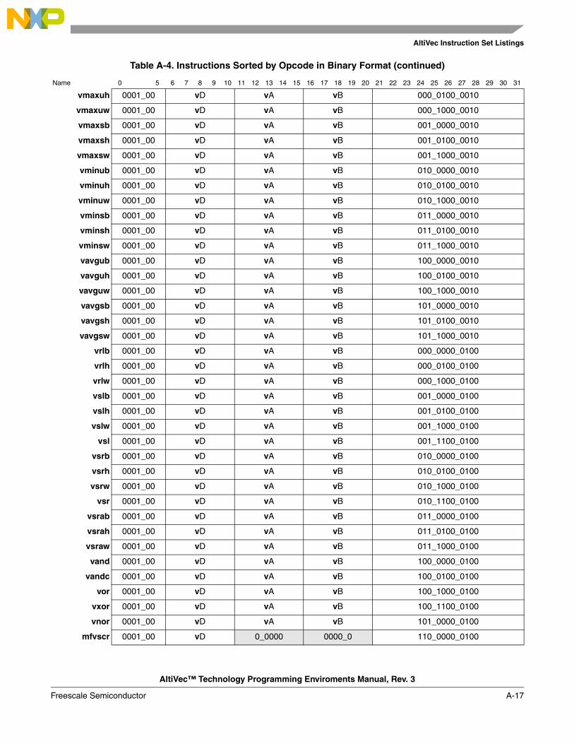
AltiVec Instruction Set Listings
AltiVec™ Technology Programming Enviroments Manual, Rev. 3
Freescale Semiconductor A-17
vmaxuh 0001_00 vD vA vB 000_0100_0010
vmaxuw 0001_00 vD vA vB 000_1000_0010
vmaxsb 0001_00 vD vA vB 001_0000_0010
vmaxsh 0001_00 vD vA vB 001_0100_0010
vmaxsw 0001_00 vD vA vB 001_1000_0010
vminub 0001_00 vD vA vB 010_0000_0010
vminuh 0001_00 vD vA vB 010_0100_0010
vminuw 0001_00 vD vA vB 010_1000_0010
vminsb 0001_00 vD vA vB 011_0000_0010
vminsh 0001_00 vD vA vB 011_0100_0010
vminsw 0001_00 vD vA vB 011_1000_0010
vavgub 0001_00 vD vA vB 100_0000_0010
vavguh 0001_00 vD vA vB 100_0100_0010
vavguw 0001_00 vD vA vB 100_1000_0010
vavgsb 0001_00 vD vA vB 101_0000_0010
vavgsh 0001_00 vD vA vB 101_0100_0010
vavgsw 0001_00 vD vA vB 101_1000_0010
vrlb 0001_00 vD vA vB 000_0000_0100
vrlh 0001_00 vD vA vB 000_0100_0100
vrlw 0001_00 vD vA vB 000_1000_0100
vslb 0001_00 vD vA vB 001_0000_0100
vslh 0001_00 vD vA vB 001_0100_0100
vslw 0001_00 vD vA vB 001_1000_0100
vsl 0001_00 vD vA vB 001_1100_0100
vsrb 0001_00 vD vA vB 010_0000_0100
vsrh 0001_00 vD vA vB 010_0100_0100
vsrw 0001_00 vD vA vB 010_1000_0100
vsr 0001_00 vD vA vB 010_1100_0100
vsrab 0001_00 vD vA vB 011_0000_0100
vsrah 0001_00 vD vA vB 011_0100_0100
vsraw 0001_00 vD vA vB 011_1000_0100
vand 0001_00 vD vA vB 100_0000_0100
vandc 0001_00 vD vA vB 100_0100_0100
vor 0001_00 vD vA vB 100_1000_0100
vxor 0001_00 vD vA vB 100_1100_0100
vnor 0001_00 vD vA vB 101_0000_0100
mfvscr 0001_00 vD 0_0000 0000_0 110_0000_0100
Table A-4. Instructions Sorted by Opcode in Binary Format (continued)
Name 0---------------5 6 7 8 9 10 11 12 13 14 15 16 17 18 19 20 21 22 23 24 25 26 27 28 29 30 31
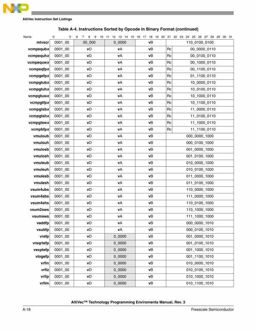
AltiVec Instruction Set Listings
AltiVec™ Technology Programming Enviroments Manual, Rev. 3
A-18 Freescale Semiconductor
mtvscr 0001_00 00_000 0_0000 vB 110_0100_0100
vcmpequbx 0001_00 vD vA vB Rc 00_0000_0110
vcmpequhx 0001_00 vD vA vB Rc 00_0100_0110
vcmpequwx 0001_00 vD vA vB Rc 00_1000_0110
vcmpeqfpx 0001_00 vD vA vB Rc 00_1100_0110
vcmpgefpx 0001_00 vD vA vB Rc 01_1100_0110
vcmpgtubx 0001_00 vD vA vB Rc 10_0000_0110
vcmpgtuhx 0001_00 vD vA vB Rc 10_0100_0110
vcmpgtuwx 0001_00 vD vA vB Rc 10_1000_0110
vcmpgtfpx 0001_00 vD vA vB Rc 10_1100_0110
vcmpgtsbx 0001_00 vD vA vB Rc 11_0000_0110
vcmpgtshx 0001_00 vD vA vB Rc 11_0100_0110
vcmpgtswx 0001_00 vD vA vB Rc 11_1000_0110
vcmpbfpx 0001_00 vD vA vB Rc 11_1100_0110
vmuloub 0001_00 vD vA vB 000_0000_1000
vmulouh 0001_00 vD vA vB 000_0100_1000
vmulosb 0001_00 vD vA vB 001_0000_1000
vmulosh 0001_00 vD vA vB 001_0100_1000
vmuleub 0001_00 vD vA vB 010_0000_1000
vmuleuh 0001_00 vD vA vB 010_0100_1000
vmulesb 0001_00 vD vA vB 011_0000_1000
vmulesh 0001_00 vD vA vB 011_0100_1000
vsum4ubs 0001_00 vD vA vB 110_0000_1000
vsum4sbs 0001_00 vD vA vB 111_0000_1000
vsum4shs 0001_00 vD vA vB 110_0100_1000
vsum2sws 0001_00 vD vA vB 110_1000_1000
vsumsws 0001_00 vD vA vB 111_1000_1000
vaddfp 0001_00 vD vA vB 000_0000_1010
vsubfp 0001_00 vD vA vB 000_0100_1010
vrefp 0001_00 vD 0_0000 vB 001_0000_1010
vrsqrtefp 0001_00 vD 0_0000 vB 001_0100_1010
vexptefp 0001_00 vD 0_0000 vB 001_1000_1010
vlogefp 0001_00 vD 0_0000 vB 001_1100_1010
vrfin 0001_00 vD 0_0000 vB 010_0000_1010
vrfiz 0001_00 vD 0_0000 vB 010_0100_1010
vrfip 0001_00 vD 0_0000 vB 010_1000_1010
vrfim 0001_00 vD 0_0000 vB 010_1100_1010
Table A-4. Instructions Sorted by Opcode in Binary Format (continued)
Name 0---------------5 6 7 8 9 10 11 12 13 14 15 16 17 18 19 20 21 22 23 24 25 26 27 28 29 30 31

AltiVec Instruction Set Listings
AltiVec™ Technology Programming Enviroments Manual, Rev. 3
Freescale Semiconductor A-19
vcfux 0001_00 vD UIMM vB 011_0000_1010
vcfsx 0001_00 vD UIMM vB 011_0100_1010
vctuxs 0001_00 vD UIMM vB 011_1000_1010
vctsxs 0001_00 vD UIMM vB 011_1100_1010
vmaxfp 0001_00 vD vA vB 100_0000_1010
vminfp 0001_00 vD vA vB 100_0100_1010
vmrghb 0001_00 vD vA vB 000_0000_1100
vmrghh 0001_00 vD vA vB 000_0100_1100
vmrghw 0001_00 vD vA vB 000_1000_1100
vmrglb 0001_00 vD vA vB 001_0000_1100
vmrglh 0001_00 vD vA vB 001_0100_1100
vmrglw 0001_00 vD vA vB 001_1000_1100
vspltb 0001_00 vD UIMM vB 010_0000_1100
vsplth 0001_00 vD UIMM vB 010_0100_1100
vspltw 0001_00 vD UIMM vB 010_1000_1100
vspltisb 0001_00 vD SIMM 0000_0 011_0000_1100
vspltish 0001_00 vD SIMM 0000_0 011_0100_1100
vspltisw 0001_00 vD SIMM 0000_0 011_1000_1100
vslo 0001_00 vD vA vB 100_0000_1100
vsro 0001_00 vD vA vB 100_0100_1100
vpkuhum 0001_00 vD vA vB 000_0000_1110
vpkuwum 0001_00 vD vA vB 000_0100_1110
vpkuhus 0001_00 vD vA vB 000_1000_1110
vpkuwus 0001_00 vD vA vB 000_1100_1110
vpkshus 0001_00 vD vA vB 001_0000_1110
vpkswus 0001_00 vD vA vB 001_0100_1110
vpkshss 0001_00 vD vA vB 001_1000_1110
vpkswss 0001_00 vD vA vB 001_1100_1110
vupkhsb 0001_00 vD 0_0000 vB 010_0000_1110
vupkhsh 0001_00 vD 0_0000 vB 010_0100_1110
vupklsb 0001_00 vD 0_0000 vB 010_1000_1110
vupklsh 0001_00 vD 0_0000 vB 010_1100_1110
vpkpx 0001_00 vD vA vB 0110000_1110
vupkhpx 0001_00 vD 0_0000 vB 011_0100_1110
vupklpx 0001_00 vD 0_0000 vB 011_1100_1110
lvsl 0111_11 vD A B 000_0000_110 0
lvsr 0111_11 vD A B 000_0100_110 0
Table A-4. Instructions Sorted by Opcode in Binary Format (continued)
Name 0---------------5 6 7 8 9 10 11 12 13 14 15 16 17 18 19 20 21 22 23 24 25 26 27 28 29 30 31

AltiVec Instruction Set Listings
AltiVec™ Technology Programming Enviroments Manual, Rev. 3
A-20 Freescale Semiconductor
dst 0111_11 0 0_0 STRM A B 010_1010_110 0
dstt 0111_1 1 0_0 STRM A B 010_1010_110 0
dstst 0111_11 0 0_0 STRM A B 010_1110_110 0
dststt 0111_11 1 0_0 STRM A B 010_1110_110 0
dss 0111_11 0 0_0 STRM 0_0000 0000_0 110_0110_110 0
dssall 0111_11 1 0_0 STRM 0_0000 0000_0 110_0110_110 0
lvebx 0111_11 vD A B 000_0000_111 0
lvehx 0111_11 vD A B 000_0100_111 0
lvewx 0111_11 vD A B 000_1000_111 0
lvx 0111_11 vD A B 000_1100_111 0
lvxl 0111_11 vD A B 010_1100_111 0
stvebx 0111_11 vS A B 001_0000_111 0
stvehx 0111_11 vS A B 001_0100_111 0
stvewx 0111_11 vS A B 001_1000_111 0
stvx 0111_11 vS A B 001_1100_111 0
stvxl 0111_11 vS A B 011_1100_111 0
Table A-4. Instructions Sorted by Opcode in Binary Format (continued)
Name 0---------------5 6 7 8 9 10 11 12 13 14 15 16 17 18 19 20 21 22 23 24 25 26 27 28 29 30 31

AltiVec Instruction Set Listings
AltiVec™ Technology Programming Enviroments Manual, Rev. 3
Freescale Semiconductor A-21
A.5 Instructions Sorted by FormTable A-5 through Table A-8 list the AltiVec instructions grouped by form.
Table A-5. VA-Form
OPCD vD vA vB vC3.5 XO
OPCD vD vA vB 0 SH XO
Specific Instructions
Name 0 5 6 7 8 9 10 11 12 13 14 15 16 17 18 19 20 21 22 23 24 25 26 27 28 29 30 31
vmhaddshs 04 vD vA vB vC 32
vmhraddshs 04 vD vA vB vC 33
vmladduhm 04 vD vA vB vC 34
vmsumubm 04 vD vA vB vC 36
vmsummbm 04 vD vA vB vC 37
vmsumuhm 04 vD vA vB vC 38
vmsumuhs 04 vD vA vB vC 39
vmsumshm 04 vD vA vB vC 40
vmsumshs 04 vD vA vB vC 41
vsel 04 vD vA vB vC 42
vperm 04 vD vA vB vC 43
vsldoi 04 vD vA vB 0 SH 44
vmaddfp 04 vD vA vB vC 46
vnmsubfp 04 vD vA vB vC 47
Table A-6. VX-Form
OPCD vD vA vB XO
OPCD vD 0_0000 0000_0 XO 0
OPCD 00_000 0_0000 vB XO 0
OPCD vD 0_0000 vB XO
OPCD vD UIMM vB XO
OPCD vD SIMM 0000_0 XO
Specific Instructions
Name 0 5 6 7 8 9 10 11 12 13 14 15 16 17 18 19 20 21 22 23 24 25 26 27 28 29 30 31
vaddubm 04 vD vA vB 0
vadduhm 04 vD vA vB 64
vadduwm 04 vD vA vB 128
vaddcuw 04 vD vA vB 384
vaddubs 04 vD vA vB 512
vadduhs 04 vD vA vB 576
vadduws 04 vD vA vB 640
vaddsbs 04 vD vA vB 768
vaddshs 04 vD vA vB 832

AltiVec Instruction Set Listings
AltiVec™ Technology Programming Enviroments Manual, Rev. 3
A-22 Freescale Semiconductor
Specific Instructions
Name 0 5 6 7 8 9 10 11 12 13 14 15 16 17 18 19 20 21 22 23 24 25 26 27 28 29 30 31
vaddsws 04 vD vA vB 896
vsububm 04 vD vA vB 1024
vsubuhm 04 vD vA vB 1088
vsubuwm 04 vD vA vB 1152
vsubcuw 04 vD vA vB 1408
vsububs 04 vD vA vB 1536
vsubuhs 04 vD vA vB 1600
vsubuws 04 vD vA vB 1664
vsubsbs 04 vD vA vB 1792
vsubshs 04 vD vA vB 1856
vsubsws 04 vD vA vB 1920
vmaxub 04 vD vA vB 2
vmaxuh 04 vD vA vB 66
vmaxuw 04 vD vA vB 130
vmaxsb 04 vD vA vB 258
vmaxsh 04 vD vA vB 322
vmaxsw 04 vD vA vB 386
vminub 04 vD vA vB 514
vminuh 04 vD vA vB 578
vminuw 04 vD vA vB 642
vminsb 04 vD vA vB 770
vminsh 04 vD vA vB 834
vminsw 04 vD vA vB 898
vavgub 04 vD vA vB 1026
vavguh 04 vD vA vB 1090
vavguw 04 vD vA vB 1154
vavgsb 04 vD vA vB 1282
vavgsh 04 vD vA vB 1346
vavgsw 04 vD vA vB 1410
vrlb 04 vD vA vB 4
vrlh 04 vD vA vB 68
vrlw 04 vD vA vB 132
vslb 04 vD vA vB 260
vslh 04 vD vA vB 324
vslw 04 vD vA vB 388
vsl 04 vD vA vB 452
vsrb 04 vD vA vB 516
vsrh 04 vD vA vB 580
vsrw 04 vD vA vB 644
Table A-6. VX-Form (continued)

AltiVec Instruction Set Listings
AltiVec™ Technology Programming Enviroments Manual, Rev. 3
Freescale Semiconductor A-23
Specific Instructions
Name 0 5 6 7 8 9 10 11 12 13 14 15 16 17 18 19 20 21 22 23 24 25 26 27 28 29 30 31
vsr 04 vD vA vB 708
vsrab 04 vD vA vB 772
vsrah 04 vD vA vB 836
vsraw 04 vD vA vB 900
vand 04 vD vA vB 1028
vandc 04 vD vA vB 1092
vor 04 vD vA vB 1156
vnor 04 vD vA vB 1284
mfvscr 04 vD 0_0000 0000_0 1540
mtvscr 04 00_000 0_0000 vB 1604
vmuloub 04 vD vA vB 8
vmulouh 04 vD vA vB 72
vmulosb 04 vD vA vB 264
vmulosh 04 vD vA vB 328
vmuleub 04 vD vA vB 520
vmuleuh 04 vD vA vB 584
vmulesb 04 vD vA vB 776
vmulesh 04 vD vA vB 840
vsum4ubs 04 vD vA vB 1544
vsum4sbs 04 vD vA vB 1800
vsum4shs 04 vD vA vB 1608
vsum2sws 04 vD vA vB 1672
vsumsws 04 vD vA vB 1928
vaddfp 04 vD vA vB 10
vsubfp 04 vD vA vB 74
vrefp 04 vD 0_0000 vB 266
vrsqrtefp 04 vD 0_0000 vB 330
vexptefp 04 vD 0_0000 vB 394
vlogefp 04 vD 0_0000 vB 458
vrfin 04 vD 0_0000 vB 522
vrfiz 04 vD 0_0000 vB 586
vrfip 04 vD 0_0000 vB 650
vrfim 04 vD 0_0000 vB 714
vcfux 04 vD UIMM vB 778
vcfsx 04 vD UIMM vB 842
vctuxs 04 vD UIMM vB 906
vctsxs 04 vD UIMM vB 970
vmaxfp 04 vD vA vB 1034
vminfp 04 vD vA vB 1098
Table A-6. VX-Form (continued)
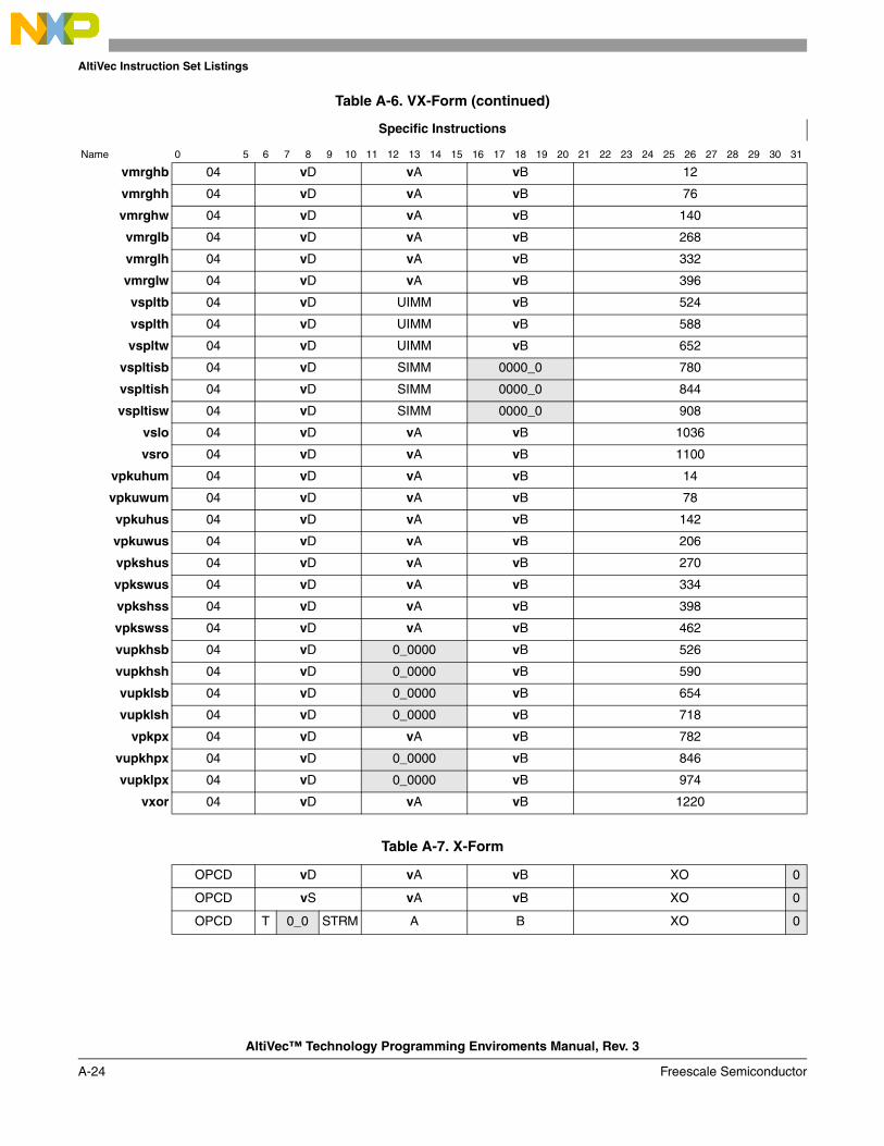
AltiVec Instruction Set Listings
AltiVec™ Technology Programming Enviroments Manual, Rev. 3
A-24 Freescale Semiconductor
Specific Instructions
Name 0 5 6 7 8 9 10 11 12 13 14 15 16 17 18 19 20 21 22 23 24 25 26 27 28 29 30 31
vmrghb 04 vD vA vB 12
vmrghh 04 vD vA vB 76
vmrghw 04 vD vA vB 140
vmrglb 04 vD vA vB 268
vmrglh 04 vD vA vB 332
vmrglw 04 vD vA vB 396
vspltb 04 vD UIMM vB 524
vsplth 04 vD UIMM vB 588
vspltw 04 vD UIMM vB 652
vspltisb 04 vD SIMM 0000_0 780
vspltish 04 vD SIMM 0000_0 844
vspltisw 04 vD SIMM 0000_0 908
vslo 04 vD vA vB 1036
vsro 04 vD vA vB 1100
vpkuhum 04 vD vA vB 14
vpkuwum 04 vD vA vB 78
vpkuhus 04 vD vA vB 142
vpkuwus 04 vD vA vB 206
vpkshus 04 vD vA vB 270
vpkswus 04 vD vA vB 334
vpkshss 04 vD vA vB 398
vpkswss 04 vD vA vB 462
vupkhsb 04 vD 0_0000 vB 526
vupkhsh 04 vD 0_0000 vB 590
vupklsb 04 vD 0_0000 vB 654
vupklsh 04 vD 0_0000 vB 718
vpkpx 04 vD vA vB 782
vupkhpx 04 vD 0_0000 vB 846
vupklpx 04 vD 0_0000 vB 974
vxor 04 vD vA vB 1220
Table A-7. X-Form
OPCD vD vA vB XO 0
OPCD vS vA vB XO 0
OPCD T 0_0 STRM A B XO 0
Table A-6. VX-Form (continued)

AltiVec Instruction Set Listings
AltiVec™ Technology Programming Enviroments Manual, Rev. 3
Freescale Semiconductor A-25
Specific Instructions
Name 0 5 6 7 8 9 10 11 12 13 14 15 16 17 18 19 20 21 22 23 24 25 26 27 28 29 30 31
dst 31 T 0_0 STRM A B 342 0
dstt 31 1 0_0 STRM A B 342 0
dstst 31 T 0_0 STRM A B 374 0
dststt 31 1 0_0 STRM A B 374 0
dss 31 A 0_0 STRM 0_0000 0000_0 822 0
dssall 31 1 0_0 STRM 0_0000 0000_0 822 0
lvebx 31 vD A B 7 0
lvehx 31 vD A B 39 0
lvewx 31 vD A B 71 0
lvsl 31 vD A B 6 0
lvsr 31 vD A B 38 0
lvx 31 vD A B 103 0
lvxl 31 vD A B 359 0
stvebx 31 vS A B 135 0
stvehx 31 vS A B 167 0
stvewx 31 vS A B 199 0
stvx 31 vS A B 231 0
stvxl 31 vS A B 487 0
Table A-8. VXR-Form
OPCD vD vA vB Rc XO
Specific Instructions
Name 0 5 6 7 8 9 10 11 12 13 14 15 16 17 18 19 20 21 22 23 24 25 26 27 28 29 30 31
vcmpbfpx 04 vD vA vB Rc 966
vcmpeqfpx 04 vD vA vB Rc 198
vcmpequbx 04 vD vA vB Rc 6
vcmpequhx 04 vD vA vB Rc 70
vcmpequwx 04 vD vA vB Rc 134
vcmpgefpx 04 vD vA vB Rc 454
vcmpgtfpx 04 vD vA vB Rc 710
vcmpgtsbx 04 vD vA vB Rc 774
vcmpgtshx 04 vD vA vB Rc 838
vcmpgtswx 04 vD vA vB Rc 902
vcmpgtubx 04 vD vA vB Rc 518
vcmpgtuhx 04 vD vA vB Rc 582
vcmpgtuwx 04 vD vA vB Rc 646
Table A-7. X-Form (continued)
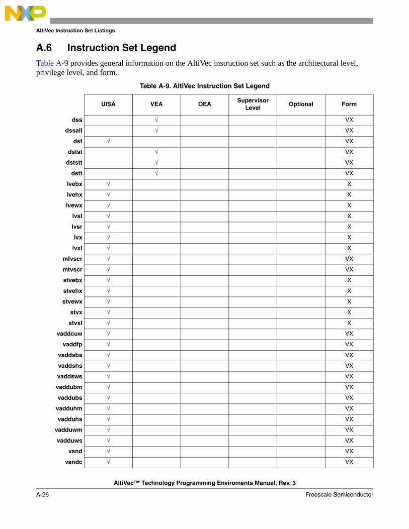
AltiVec Instruction Set Listings
AltiVec™ Technology Programming Enviroments Manual, Rev. 3
A-26 Freescale Semiconductor
A.6 Instruction Set LegendTable A-9 provides general information on the AltiVec instruction set such as the architectural level, privilege level, and form.
Table A-9. AltiVec Instruction Set Legend
UISA VEA OEASupervisor
LevelOptional Form
dss √ VX
dssall √ VX
dst √ VX
dstst √ VX
dststt √ VX
dstt √ VX
lvebx √ X
lvehx √ X
lvewx √ X
lvsl √ X
lvsr √ X
lvx √ X
lvxl √ X
mfvscr √ VX
mtvscr √ VX
stvebx √ X
stvehx √ X
stvewx √ X
stvx √ X
stvxl √ X
vaddcuw √ VX
vaddfp √ VX
vaddsbs √ VX
vaddshs √ VX
vaddsws √ VX
vaddubm √ VX
vaddubs √ VX
vadduhm √ VX
vadduhs √ VX
vadduwm √ VX
vadduws √ VX
vand √ VX
vandc √ VX

AltiVec Instruction Set Listings
AltiVec™ Technology Programming Enviroments Manual, Rev. 3
Freescale Semiconductor A-27
vavgsb √ VX
vavgsh √ VX
vavgsw √ VX
vavgub √ VX
vavguh √ VX
vavguw √ VX
vcfux √ VX
vcfsx √ VX
vcmpbfpx √ VXR
vcmpeqfpx √ VXR
vcmpequbx √ VXR
vcmpequhx √ VXR
vcmpequwx √ VXR
vcmpgefpx √ VXR
vcmpgtfpx √ VXR
vcmpgtsbx √ VXR
vcmpgtshx √ VXR
vcmpgtswx √ VXR
vcmpgtubx √ VXR
vcmpgtuhx √ VXR
vcmpgtuwx √ VXR
vctsxs √ VX
vctuxs √ VX
vexptefp √ VX
vlogefp √ VX
vmaddfp √ VA
vmaxfp √ VX
vmaxsb √ VX
vmaxsh √ VX
vmaxsw √ VX
vmaxub √ VX
vmaxuh √ VX
vmaxuw √ VX
vmhaddshs √ VA
vmhraddshs √ VA
vminfp √ VX
Table A-9. AltiVec Instruction Set Legend (continued)
UISA VEA OEASupervisor
LevelOptional Form
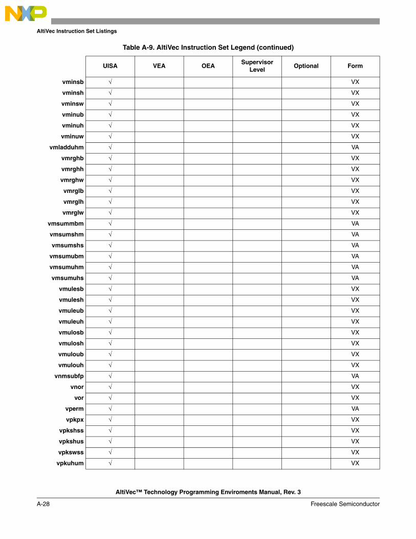
AltiVec Instruction Set Listings
AltiVec™ Technology Programming Enviroments Manual, Rev. 3
A-28 Freescale Semiconductor
vminsb √ VX
vminsh √ VX
vminsw √ VX
vminub √ VX
vminuh √ VX
vminuw √ VX
vmladduhm √ VA
vmrghb √ VX
vmrghh √ VX
vmrghw √ VX
vmrglb √ VX
vmrglh √ VX
vmrglw √ VX
vmsummbm √ VA
vmsumshm √ VA
vmsumshs √ VA
vmsumubm √ VA
vmsumuhm √ VA
vmsumuhs √ VA
vmulesb √ VX
vmulesh √ VX
vmuleub √ VX
vmuleuh √ VX
vmulosb √ VX
vmulosh √ VX
vmuloub √ VX
vmulouh √ VX
vnmsubfp √ VA
vnor √ VX
vor √ VX
vperm √ VA
vpkpx √ VX
vpkshss √ VX
vpkshus √ VX
vpkswss √ VX
vpkuhum √ VX
Table A-9. AltiVec Instruction Set Legend (continued)
UISA VEA OEASupervisor
LevelOptional Form

AltiVec Instruction Set Listings
AltiVec™ Technology Programming Enviroments Manual, Rev. 3
Freescale Semiconductor A-29
vpkuhus √ VX
vpkswus √ VX
vpkuwum √ VX
vpkuwus √ VX
vrefp √ VX
vrfim √ VX
vrfin √ VX
vrfip √ VX
vrfiz √ VX
vrlb √ VX
vrlh √ VX
vrlw √ VX
vrsqrtefp √ VX
vsel √ VA
vsl √ VX
vslb √ VX
vsldoi √ VA
vslh √ VX
vslo √ VX
vslw √ VX
vspltb √ VX
vsplth √ VX
vspltisb √ VX
vspltish √ VX
vspltisw √ VX
vspltw √ VX
vsr √ VX
vsrab √ VX
vsrah √ VX
vsraw √ VX
vsrb √ VX
vsrh √ VX
vsro √ VX
vsrw √ VX
vsubcuw √ VX
vsubfp √ VX
Table A-9. AltiVec Instruction Set Legend (continued)
UISA VEA OEASupervisor
LevelOptional Form
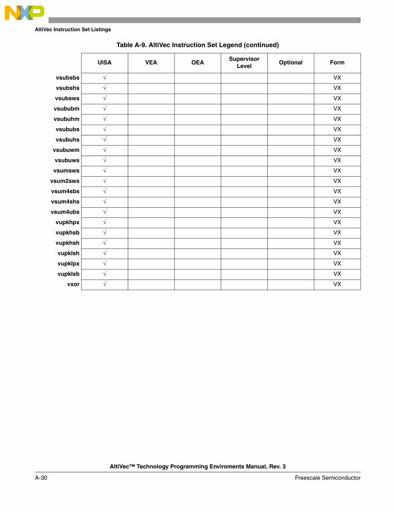
AltiVec Instruction Set Listings
AltiVec™ Technology Programming Enviroments Manual, Rev. 3
A-30 Freescale Semiconductor
vsubsbs √ VX
vsubshs √ VX
vsubsws √ VX
vsububm √ VX
vsubuhm √ VX
vsububs √ VX
vsubuhs √ VX
vsubuwm √ VX
vsubuws √ VX
vsumsws √ VX
vsum2sws √ VX
vsum4sbs √ VX
vsum4shs √ VX
vsum4ubs √ VX
vupkhpx √ VX
vupkhsb √ VX
vupkhsh √ VX
vupklsh √ VX
vupklpx √ VX
vupklsb √ VX
vxor √ VX
Table A-9. AltiVec Instruction Set Legend (continued)
UISA VEA OEASupervisor
LevelOptional Form

AltiVec™ Technology Programming Enviroments Manual, Rev. 3
Freescale Semiconductor B-1
Appendix BRevision HistoryThis appendix provides a list of the major differences between revisions of the AltiVec Programming Environments Manual.
B.1 Changes from Revision 2 to Revision 3Major changes to the AltiVec Programming Environments Manual, from Revision 2 to Revision 3 are as follows:Section, Page ChangesBook Updated template to Freescale. Section 6 Minor updates to figures to provide a better explanation of the instructions.3.1.6.1, 3-8 Updated the code examples in these two sections. The code was updated in order3.1.6.2, 3-10 to avoid having the target address possibly point to an invalid address that is an
unmapped page in memory. This is avoided by using addr + 15 in the second load instead of addr + 16. If an address is 16-byte aligned then the first load (addr + 0) and second load (addr + 16) will point to the same aligned quad word and avoid the second address from being invalid.
B.2 Changes from Revision 1 to Revision 2Only minor formatting upgrades were made to the AltiVec Programming Environments Manual, from Revision 1 to Revision 2.

Revision History
AltiVec™ Technology Programming Enviroments Manual, Rev. 3
B-2 Freescale Semiconductor
B.3 Changes from Revision 0 to Revision 1Major changes to the AltiVec Programming Environments Manual, from Revision 0 to Revision 1 are as follows:Section, Page Changes2.1.2, 2-4 Replace Figure 2-4, “Saving/Restoring the AltiVec Context Register (VRSAVE),”
with the following:
2.2, 2-9 Figure 2-10—The vector registers are 128 bits wide not 64 bits wide as shown.4.2.2.4, 4-20 Change Table 4-9 as follows
The mnemonic for Vector Round to Floating-Point Integer Nearest should be vrfin, not fvrfin.The mnemonic for Vector Round to Floating-Point Integer toward Zero should be vrfiz, not fvrfiz.The mnemonic for Vector Round to Floating-Point Integer toward Positive Infinity should be vrfip, not fvrfip.The mnemonic for Vector Round to Floating-Point Integer toward Minus Infinity should be vrfim, not fvrfim.
6.2, 6-24 Change the mfvscr encoding as shown below (note: bit 31 is not 0):
6.2, 6-25 Change the mtvscr encoding as shown below (note: bit 31 is not 0):
A.1, Page A-2 Change the mfvscr encoding as shown below (note: bit 31 is not 0):
0 1 2 3 4 5 6 7 8 9 10 11 12 13 14 15
Field VR0 VR1 VR2 VR3 VR4 VR5 VR6 VR7 VR8 VR9 VR10 VR11 VR12 VR13 VR14 VR15
Reset 0000_0000_0000_0000
R/W R/W using mfspr or mtspr instructions
16 17 18 19 20 21 22 23 24 25 26 27 28 29 30 31
Field VR16 VR17 VR18 VR19 VR20 VR21 VR22 VR23 VR24 VR25 VR26 VR27 VR28 VR29 VR30 VR31
Reset 0000_0000_0000_0000
R/W R/W using mfspr or mtspr instructions
SPR SPR256
04 vD 0 0 0 0 0 0 0 0 0 0 1540
0 5 6 10 11 15 16 20 21 31
04 0 0 0 0 0 0 0 0 0 0 vB 1604
0 5 6 10 11 15 16 20 21 31
mfvscr 04 vD 0 0 0 0 0 0 0 0 0 0 1540

Revision History
AltiVec™ Technology Programming Enviroments Manual, Rev. 3
Freescale Semiconductor B-3
A.1, Page A-2 Change the mtvscr encoding as shown below (note: bit 31 is not 0 and vD should be vB):
A.2, Page A-9 Change the mfvscr encoding as shown below (note: bit 31 is not 0):
A.2, Page A-9 Change the mtvscr encoding as shown below (note: bit 31 is not 0):
A.3, Page A-14 Change the mfvscr encoding as shown below (note: bit 31 is not 0):
A.3, Page A-14 Change the mtvscr encoding as shown below (note: bit 31 is not 0):
mtvscr 04 0 0 0 0 0 0 0 0 0 0 vB 1604
mfvscr 000100 vD 0 0 0 0 0 0 0 0 0 0 110 0000 0100
mtvscr 000100 0 0 0 0 0 0 0 0 0 0 vB 110 0100 0100
mfvscr 04 vD 0 0 0 0 0 0 0 0 0 0 1540
mtvscr 04 0 0 0 0 0 0 0 0 0 0 vB 1604

Revision History
AltiVec™ Technology Programming Enviroments Manual, Rev. 3
B-4 Freescale Semiconductor

AltiVec™ Technology Programming Enviroments Manual, Rev. 3
Freescale Semiconductor Glossary-1
GlossaryThe glossary contains an alphabetical list of terms, phrases, and abbreviations used in this book. Some of the terms and definitions included in the glossary are reprinted from IEEE Std 754-1985, IEEE Standard for Binary Floating-Point Arithmetic, copyright ©1985 by the Institute of Electrical and Electronics Engineers, Inc. with the permission of the IEEE.
A Architecture. A detailed specification of requirements for a processor or computer system. It does not specify details of how the processor or computer system must be implemented; instead it provides a template for a family of compatible implementations.
Asynchronous exception. Exceptions that are caused by events external to the processor’s execution. In this document, the term ‘asynchronous exception’ is used interchangeably with the word interrupt.
Atomic access. A bus access that attempts to be part of a read-write operation to the same address uninterrupted by any other access to that address (the term refers to the fact that the transactions are indivisible). The PowerPC architecture implements atomic accesses through the lwarx/stwcx. instruction pair.
B BAT (block address translation) mechanism. A software-controlled array that stores the available block address translations on-chip.
Biased exponent. An exponent whose range of values is shifted by a constant (bias). Typically a bias is provided to allow a range of positive values to express a range that includes both positive and negative values.
Big-endian. A byte-ordering method in memory where the address n of a word corresponds to the most-significant byte. In an addressed memory word, the bytes are ordered (left to right) 0, 1, 2, 3, with 0 being the most-significant byte. See Little-endian.
Block. An area of memory that ranges from 128 Kbytes to 256 Mbytes whose size, translation, and protection attributes are controlled by the BAT mechanism.
Boundedly undefined. A characteristic of certain operation results that are not rigidly prescribed by the PowerPC architecture. Boundedly-undefined results for a given operation may vary among implementations and between execution attempts in the same implementation.

Glossary
AltiVec™ Technology Programming Enviroments Manual, Rev. 3
Glossary-2 Freescale Semiconductor
Although the architecture does not prescribe the exact behavior for when results are allowed to be boundedly undefined, the results of executing instructions in contexts where results are allowed to be boundedly undefined are constrained to ones that could have been achieved by executing an arbitrary sequence of defined instructions, in valid form, starting in the state the machine was in before attempting to execute the given instruction.
Branch folding. The replacement with target instructions of a branch instruction and any instructions along the not-taken path when a branch is either taken or predicted as taken.
Branch prediction. The process of guessing whether a branch will be taken. Such predictions can be correct or incorrect; the term ‘predicted’ as it is used here does not imply that the prediction is correct (successful). The PowerPC architecture defines a means for static branch prediction as part of the instruction encoding.
Branch resolution. The determination of whether a branch is taken or not taken. A branch is said to be resolved when the processor can determine which instruction path to take. If the branch is resolved as predicted, the instructions following the predicted branch that may have been speculatively executed can complete. If the branch is not resolved as predicted, instructions on the mispredicted path, and any results of speculative execution, are purged from the pipeline and fetching continues from the nonpredicted path.
Burst. A multiple-beat data transfer whose total size is typically equal to a cache block.
Bus clock. Clock that causes the bus state transitions.
Bus master. The owner of the address or data bus; the device that initiates or requests the transaction.
C Cache. High-speed memory containing recently accessed data or instructions (subset of main memory).
Cache block. A small region of contiguous memory that is copied from memory into a cache. The size of a cache block may vary among processors; the maximum block size is one page. In PowerPC processors, cache coherency is maintained on a cache-block basis. Note that the term ‘cache block’ is often used interchangeably with ‘cache line.’
Cache coherency. An attribute wherein an accurate and common view of memory is provided to all devices that share the same memory system. Caches are coherent if a processor performing a read from its cache is supplied with data corresponding to the most recent value written to memory or to another processor’s cache.
Glossary
AltiVec™ Technology Programming Enviroments Manual, Rev. 3
Freescale Semiconductor Glossary-3
Cache flush. An operation that removes from a cache any data from a specified address range. This operation ensures that any modified data within the specified address range is written back to main memory. This operation is generated typically by a Data Cache Block Flush (dcbf) instruction.
Caching-inhibited. A memory update policy in which the cache block is bypassed and the load or store is performed to or from main memory.
Cast out. A cache block that must be written to memory when a cache miss causes a cache block to be replaced.
Change bit. One of two page history bits found in each page table entry (PTE). The processor sets the change bit if any store is performed into the page. See also Reference.
Clean. An operation that causes a cache block to be written to memory, if modified, and then left in a valid, unmodified state in the cache.
Clear. To cause a bit or bit field to register a value of zero. See also Set.
Context synchronization. An operation that ensures that all instructions in execution complete past the point where they can produce an exception, that all instructions in execution complete in the context in which they began execution, and that all subsequent instructions are fetched and executed in the new context. Context synchronization may result from executing specific instructions (such as isync or rfi) or when certain events occur (such as an exception).
Copy-back operation. A cache operation in which a cache line is copied back to memory to enforce cache coherency. Copy-back operations consist of snoop push-out operations and cache cast-out operations.
D Deadline Scheduling. Deadline scheduling determines the execution order of tasks based on their deadlines.
Denormalized number. A nonzero floating-point number whose exponent has a reserved value, usually the format's minimum, and whose explicit or implicit leading significand bit is zero.
Direct-mapped cache. A cache in which each main memory address can appear in only one location within the cache, operates more quickly when the memory request is a cache hit.
Direct-store segment access. An access to an I/O address space. The MPC603 defines separate memory-mapped and I/O address spaces, or segments, distinguished by the corresponding segment register T bit in the address translation logic of the MPC603. If the T bit is cleared, the memory reference is a normal memory-mapped access and can use the virtual memory management hardware of the MPC603. If the T bit is set, the memory reference is a direct-store access.

Glossary
AltiVec™ Technology Programming Enviroments Manual, Rev. 3
Glossary-4 Freescale Semiconductor
Double-word swap. AltiVec processors implement a double-word swap when moving quad words between vector registers and memory. The double word swap performs an additional swap to keep vector registers and memory consistent in little-endian mode. Double-word swap is referred to as ‘swizzling’ in the AltiVec technology architecture specification. This feature is not supported by the PowerPC architecture.
E Effective address (EA). The 32-bit address specified for a load, store, or an instruction fetch. This address is then submitted to the MMU for translation to either a physical memory address.
Exception. A condition encountered by the processor that requires special, supervisor-level processing.
Exception handler. A software routine that executes when an exception is taken. Normally, the exception handler corrects the condition that caused the exception, or performs some other meaningful task (that may include aborting the program that caused the exception). The address for each exception handler is identified by an exception vector offset defined by the architecture and a prefix selected via the MSR.
Extended opcode. A secondary opcode field generally located in instruction bits 21–30, that further defines the instruction type. All PowerPC instructions are one word in length. The most significant 6 bits of the instruction are the Primary opcode, identifying the type of instruction. See also Primary opcode.
Exclusive state. MEI state (E) in which only one caching device contains data that is also in system memory.
Exponent. In the binary representation of a floating-point number, the exponent is the component that normally signifies the integer power to which the value two is raised in determining the value of the represented number. See also Biased exponent.
F Fetch. Retrieving instructions from either the cache or main memory and placing them into the instruction queue.
Floating-point register (FPR). Any of the 32 registers in the floating-point register file. These registers provide the source operands and destination results for floating-point instructions. Load instructions move data from memory to FPRs and store instructions move data from FPRs to memory. The FPRs are 64 bits wide and store floating-point values in double-precision format
Floating-point unit. The functional unit in the MPC603e processor responsible for executing all floating-point instructions.

Glossary
AltiVec™ Technology Programming Enviroments Manual, Rev. 3
Freescale Semiconductor Glossary-5
Flush. An operation that causes a cache block to be invalidated and the data, if modified, to be written to memory.
Fraction. In the binary representation of a floating-point number, the field of the significand that lies to the right of its implied binary point.
Fully associative. Addressing scheme where every cache location (every byte) can have any possible address.
G General-purpose register (GPR). Any of the 32 registers in the general-purpose register file. These registers provide the source operands and destination results for all integer data manipulation instructions. Integer load instructions move data from memory to GPRs and store instructions move data from GPRs to memory.
Guarded. The guarded attribute pertains to out-of-order execution. When a page is designated as guarded, instructions and data cannot be accessed out-of-order.
H Harvard architecture. An architectural model featuring separate caches and other memory management resources for instructions and data.
Hashing. An algorithm used in the page table search process.
I IEEE 754. A standard written by the Institute of Electrical and Electronics Engineers that defines operations and representations of binary floating-point numbers.
Illegal instructions. A class of instructions that are not implemented for a particular PowerPC processor. These include instructions not defined by the PowerPC architecture. In addition, for 32-bit implementations, instructions that are defined only for 64-bit implementations are considered to be illegal instructions. For 64-bit implementations instructions that are defined only for 32-bit implementations are considered to be illegal instructions.
Implementation. A particular processor that conforms to the PowerPC architecture, but may differ from other architecture-compliant implementations for example in design, feature set, and implementation of optional features. The PowerPC architecture has many different implementations.
Implementation-dependent. An aspect of a feature in a processor’s design that is defined by a processor’s design specifications rather than by the PowerPC architecture.
Implementation-specific. An aspect of a feature in a processor’s design that is not required by the PowerPC architecture, but for which the PowerPC architecture may provide concessions to ensure that processors that implement the feature do so consistently.
Imprecise exception. A type of synchronous exception that is allowed not to adhere to the precise exception model (see Precise exception). The PowerPC architecture allows only floating-point exceptions to be handled imprecisely.

Glossary
AltiVec™ Technology Programming Enviroments Manual, Rev. 3
Glossary-6 Freescale Semiconductor
Inexact. Loss of accuracy in an arithmetic operation when the rounded result differs from the infinitely precise value with unbounded range.
Instruction queue. A holding place for instructions fetched from the current instruction stream.
Integer unit. The functional unit in the MPC603e responsible for executing all integer instructions.
In-order. An aspect of an operation that adheres to a sequential model. An operation is said to be performed in-order if, at the time that it is performed, it is known to be required by the sequential execution model. See Out-of-order.
Instruction latency. The total number of clock cycles necessary to execute an instruction and make ready the results of that instruction.
Instruction parallelism. A feature of PowerPC processors that allows instructions to be processed in parallel.
Interrupt. An external signal that causes the MPC603e to suspend current execution and take a predefined exception.
L Latency. The number of clock cycles necessary to execute an instruction and make ready the results of that execution for a subsequent instruction.
L2 cache. See Secondary cache.
Least-significant bit (lsb). The bit of least value in an address, register, field, data element, or instruction encoding.
Least-significant byte (LSB). The byte of least value in an address, register, data element, or instruction encoding.
Little-endian. A byte-ordering method in memory where the address n of a word corresponds to the least-significant byte. In an addressed memory word, the bytes are ordered (left to right) 3, 2, 1, 0, with 3 being the most-significant byte. See Big endian.
Loop unrolling. Loop unrolling provides a way of increasing performance by allowing more instructions to be issued in a clock cycle. The compiler replicates the loop body to increase the number of instructions executed between a loop branch.
M Mantissa. The decimal part of logarithm.
MESI (modified/exclusive/shared/invalid). Cache coherency protocol used to manage caches on different devices that share a memory system. Note that the PowerPC architecture does not specify the implementation of a MESI protocol to ensure cache coherency.

Glossary
AltiVec™ Technology Programming Enviroments Manual, Rev. 3
Freescale Semiconductor Glossary-7
Memory access ordering. The specific order in which the processor performs load and store memory accesses and the order in which those accesses complete.
Memory-mapped accesses. Accesses whose addresses use the page or block address translation mechanisms provided by the MMU and that occur externally with the bus protocol defined for memory.
Memory coherency. An aspect of caching in which it is ensured that an accurate view of memory is provided to all devices that share system memory.
Memory consistency. Refers to agreement of levels of memory with respect to a single processor and system memory (for example, on-chip cache, secondary cache, and system memory).
Memory management unit (MMU). The functional unit that is capable of translating an effective (logical) address to a physical address, providing protection mechanisms, and defining caching methods.
Microarchitecture. The hardware details of a microprocessor’s design. Such details are not defined by the PowerPC architecture.
Mnemonic. The abbreviated name of an instruction used for coding.
Modified state. MEI state (M) in which one, and only one, caching device has the valid data for that address. The data at this address in external memory is not valid.
Modular Arithmetic. Arithmetic in which integers that are congruent modulo any given integer are considered equal.
Most-significant bit (msb). The highest-order bit in an address, registers, data element, or instruction encoding.
Most-significant byte (MSB). The highest-order byte in an address, registers, data element, or instruction encoding.
Munging. A modification performed on an effective address that allows it to appear to the processor that individual aligned scalars are stored as little-endian values, when in fact it is stored in big-endian order, but at different byte addresses within double words. Note that munging affects only the effective address and not the byte order. Note also that this term is not used by the PowerPC architecture.
Multiprocessing. The capability of software, especially operating systems, to support execution on more than one processor at the same time.
N NaN. An abbreviation for not a number; a symbolic entity encoded in floating-point format. There are two types of NaNs—signaling NaNs and quiet NaNs.
No-op. No-operation. A single-cycle operation that does not affect registers or generate bus activity.

Glossary
AltiVec™ Technology Programming Enviroments Manual, Rev. 3
Glossary-8 Freescale Semiconductor
Normalization. A process by which a floating-point value is manipulated such that it can be represented in the format for the appropriate precision (single- or double-precision). For a floating-point value to be representable in the single- or double-precision format, the leading implied bit must be a 1.
O OEA (operating environment architecture). The level of the architecture that describes PowerPC memory management model, supervisor-level registers, synchronization requirements, and the exception model. It also defines the time-base feature from a supervisor-level perspective. Implementations that conform to the PowerPC OEA also conform to the PowerPC UISA and VEA.
Optional. A feature, such as an instruction, a register, or an exception, that is defined by the PowerPC architecture but not required to be implemented.
Out-of-order. An aspect of an operation that allows it to be performed ahead of one that may have preceded it in the sequential model, for example, speculative operations. An operation is said to be performed out-of-order if, at the time that it is performed, it is not known to be required by the sequential execution model. See In-Order.
Out-of-order execution. A technique that allows instructions to be issued and completed in an order that differs from their sequence in the instruction stream.
Overflow. An condition that occurs during arithmetic operations when the result cannot be stored accurately in the destination register(s). For example, if two 32-bit numbers are multiplied, the result may not be representable in 32 bits. Since the 32-bit registers of the MPC603e cannot represent this sum, an overflow condition occurs.
P Page. A region in memory. The OEA defines a page as a 4-Kbyte area of memory, aligned on a 4-Kbyte boundary.
Page fault. A page fault is a condition that occurs when the processor attempts to access a memory location that does not reside within a page not currently resident in physical memory. On PowerPC processors, a page fault exception condition occurs when a matching, valid page table entry (PTE[V] = 1) cannot be located.
Page table. A table in memory is comprised of page table entries, or PTEs. It is further organized into eight PTEs per PTEG (page table entry group). The number of PTEGs in the page table depends on the size of the page table (as specified in the SDR1 register).
Page table entry (PTE). Data structures containing information used to translate effective address to physical address on a 4-Kbyte page basis. A PTE consists of 8 bytes of information in a 32-bit processor and 16 bytes of information in a 64-bit processor.
Park. The act of allowing a bus master to maintain bus mastership without having to arbitrate.

Glossary
AltiVec™ Technology Programming Enviroments Manual, Rev. 3
Freescale Semiconductor Glossary-9
Persistent data stream. A data stream is considered to be persistent when it is expected to be loaded from frequently.
Physical memory. The actual memory that can be accessed through the system’s memory bus.
Pipelining. A technique that breaks operations, such as instruction processing or bus transactions, into smaller distinct stages or tenures (respectively) so that a subsequent operation can begin before the previous one has completed.
Precise exceptions. A category of exception for which the pipeline can be stopped so instructions that preceded the faulting instruction can complete and subsequent instructions can be flushed and redispatched after exception handling has completed. See Imprecise exceptions.
Primary opcode. The most-significant 6 bits (bits 0–5) of the instruction encoding that identifies the type of instruction.
Program order. The order of instructions in an executing program. More specifically, this term is used to refer to the original order in which program instructions are fetched into the instruction queue from the cache
Protection boundary. A boundary between protection domains.
Protection domain. A protection domain is a segment, a virtual page, a BAT area, or a range of unmapped effective addresses. It is defined only when the appropriate relocate bit in the MSR (IR or DR) is 1.
Q Quad word. A group of 16 contiguous locations starting at an address divisible by 16.
Quiet NaN. A type of NaN that can propagate through most arithmetic operations without signaling exceptions. A quiet NaN is used to represent the results of certain invalid operations, such as invalid arithmetic operations on infinities or on NaNs, when invalid. See Signaling NaN.
R rA. The rA instruction field is used to specify a GPR to be used as a source or destination.
rB. The rB instruction field is used to specify a GPR to be used as a source.
rD. The rD instruction field is used to specify a GPR to be used as a destination.
rS. The rS instruction field is used to specify a GPR to be used as a source.
Real address mode. An MMU mode when no address translation is performed and the effective address specified is the same as the physical address. The processor’s MMU is operating in real address mode if its ability to perform address translation has been disabled through the MSR registers IR and/or DR bits.

Glossary
AltiVec™ Technology Programming Enviroments Manual, Rev. 3
Glossary-10 Freescale Semiconductor
Record bit. Bit 31 (or the Rc bit) in the instruction encoding. When it is set, updates the condition register (CR) to reflect the result of the operation.
Reference bit. One of two page history bits found in each page table entry (PTE). The processor sets the reference bit whenever the page is accessed for a read or write.
Register indirect addressing. A form of addressing that specifies one GPR that contains the address for the load or store.
Register indirect with immediate index addressing. A form of addressing that specifies an immediate value to be added to the contents of a specified GPR to form the target address for the load or store.
Register indirect with index addressing. A form of addressing that specifies that the contents of two GPRs be added together to yield the target address for the load or store.
Rename register. Temporary buffers used by instructions that have finished execution but have not completed.
Reservation. The processor establishes a reservation on a cache block of memory space when it executes a lwarx instruction to read a memory semaphore into a GPR.
Reservation station. A buffer between the dispatch and execute stages that allows instructions to be dispatched even though the results of instructions on which the dispatched instruction may depend are not available.
RISC (reduced instruction set computing). An architecture characterized by fixed-length instructions with nonoverlapping functionality and by a separate set of load and store instructions that perform memory accesses.
S Saturate. A value v which lies outside the range of numbers representable by a destination type is replaced by the representable number closest to v.
Secondary cache. A cache memory that is typically larger and has a longer access time than the primary cache. A secondary cache may be shared by multiple devices. Also referred to as L2, or level-2, cache.
Set (v). To write a nonzero value to a bit or bit field; the opposite of clear. The term ‘set’ may also be used to generally describe the updating of a bit or bit field.
Set (n). A subdivision of a cache. Cacheable data can be stored in a given location in one of the sets, typically corresponding to its lower-order address bits. Because several memory locations can map to the same location, cached data is typically placed in the set whose cache block corresponding to that address was used least recently. See Set associative.

Glossary
AltiVec™ Technology Programming Enviroments Manual, Rev. 3
Freescale Semiconductor Glossary-11
Set-associative. Aspect of cache organization in which the cache space is divided into sections, called sets. The cache controller associates a particular main memory address with the contents of a particular set, or region, within the cache.
Signaling NaN. A type of NaN that generates an invalid operation program exception when it is specified as arithmetic operands. See Quiet NaN.
Significand. The component of a binary floating-point number that consists of an explicit or implicit leading bit to the left of its implied binary point and a fraction field to the right.
SIMD. Single instruction stream, multiple data streams. A vector instruction can operate on several data elements within a single instruction in a single functional unit. SIMD is a way to work with all the data at once (in parallel), which can make execution faster.
Simplified mnemonics. Assembler mnemonics that represent a more complex form of a common operation.
Snooping. Monitoring addresses driven by a bus master to detect the need for coherency actions.
Snoop push. Response to a snooped transaction that hits a modified cache block. The cache block is written to memory and made available to the snooping device.
Splat. A splat instruction will take one element and replicates (splats) that value into a vector register. The purpose being to have all elements have the same value so they can be used as a constant to multiply other vector registers.
Split-transaction. A transaction with independent request and response tenures.
Split-transaction bus. A bus that allows address and data transactions from different processors to occur independently.
Stage. The term ‘stage’ is used in two different senses, depending on whether the pipeline is being discussed as a physical entity or a sequence of events. In the latter case, a stage is an element in the pipeline during which certain actions are performed, such as decoding the instruction, performing an arithmetic operation, or writing back the results. Typically, the latency of a stage is one processor clock cycle. Some events, such as dispatch, write-back, and completion, happen instantaneously and may be thought to occur at the end of a stage. An instruction can spend multiple cycles in one stage. An integer multiply, for example, takes multiple cycles in the execute stage. When this occurs, subsequent instructions may stall. An instruction may also occupy more than one stage simultaneously, especially in the sense that a stage can be seen as a physical resource—for example, when instructions are dispatched they are assigned a place in the CQ at the same time they are passed to the execute stage. They can be said to occupy both the complete and execute stages in the same clock cycle.

Glossary
AltiVec™ Technology Programming Enviroments Manual, Rev. 3
Glossary-12 Freescale Semiconductor
Stall. An occurrence when an instruction cannot proceed to the next stage.
Static branch prediction. Mechanism by which software (for example, compilers) can hint to the machine hardware about the direction a branch is likely to take.
Sticky bit. A bit that when set must be cleared explicitly.
Superscalar machine. A machine that can issue multiple instructions concurrently from a conventional linear instruction stream.
Supervisor mode. The privileged operation state of a processor. In supervisor mode, software, typically the operating system, can access all control registers and can access the supervisor memory space, among other privileged operations.
Swizzling. See Double-word swap.
Synchronization. A process to ensure that operations occur strictly in order. See Context synchronization.
Synchronous exception. An exception that is generated by the execution of a particular instruction or instruction sequence. There are two types of synchronous exceptions, precise and imprecise.
System memory. The physical memory available to a processor.
T Tenure. The period of bus mastership. For the MPC603e, there can be separate address bus tenures and data bus tenures. A tenure consists of three phases: arbitration, transfer, and termination.
TLB (translation lookaside buffer). A cache that holds recently-used page table entries.
Throughput. The measure of the number of instructions that are processed per clock cycle.
Tiny. A floating-point value that is too small to be represented for a particular precision format, including denormalized numbers; they do not include ±0.
Transaction. A complete exchange between two bus devices. A transaction is typically comprised of an address tenure and one or more data tenures, which may overlap or occur separately from the address tenure. A transaction may be minimally comprised of an address tenure only.
Transient stream. A data stream is considered to be transient when it is likely to be referenced from infrequently.

Glossary
AltiVec™ Technology Programming Enviroments Manual, Rev. 3
Freescale Semiconductor Glossary-13
U UISA (user instruction set architecture). The level of the architecture to which user-level software should conform. The UISA defines the base user-level instruction set, user-level registers, data types, floating-point memory conventions and exception model as seen by user programs, and the memory and programming models.
Underflow. A condition that occurs during arithmetic operations when the result cannot be represented accurately in the destination register. For example, underflow can happen if two floating-point fractions are multiplied and the result requires a smaller exponent and/or mantissa than the single-precision format can provide. In other words, the result is too small to be represented accurately.
User mode. The operating state of a processor used typically by application software. In user mode, software can access only certain control registers and can access only user memory space. No privileged operations can be performed. Also referred to as problem state.
V vA. The vA instruction field is used to specify a vector register to be used as a source or destination.
vB. The vB instruction field is used to specify a vector register to be used as a source.
vC. The vC instruction field is used to specify a vector register to be used as a source.
vD. The vD instruction field is used to specify a vector register to be used as a destination.
vS. The vS instruction field is used to specify a vector register to be used as a source.
VEA (virtual environment architecture). The level of the architecture that describes the memory model for an environment in which multiple devices can access memory, defines aspects of the cache model, defines cache control instructions, and defines the time-base facility from a user-level perspective. Implementations that conform to the PowerPC VEA also adhere to the UISA, but may not necessarily adhere to the OEA.
Vector. The spatial parallel processing of short, fixed-length one-dimensional matrices performed by an execution unit.
Vector Register (VR). Any of the 32 registers in the vector register file. Each vector register is 128 bits wide. These registers can provide the source operands and destination results for AltiVec instructions.
Virtual address. An intermediate address used in the translation of an effective address to a physical address.
Virtual memory. The address space created using the memory management facilities of the processor. Program access to virtual memory is possible only when it coincides with physical memory.

Glossary
AltiVec™ Technology Programming Enviroments Manual, Rev. 3
Glossary-14 Freescale Semiconductor
W Way. A location in the cache that holds a cache block, its tags and status bits.
Weak ordering. A memory access model that allows bus operations to be reordered dynamically, which improves overall performance and in particular reduces the effect of memory latency on instruction throughput.
Word. A 32-bit data element.
Write-back. A cache memory update policy in which processor write cycles are directly written only to the cache. External memory is updated only indirectly, for example, when a modified cache block is cast out to make room for newer data.
Write-through. A cache memory update policy in which all processor write cycles are written to both the cache and memory.

AltiVec™ Technology Programming Enviroments Manual, Rev. 3
Freescale Semiconductor Index-1
Index
AAcronyms and abbreviated terms, list, xxiiiAddress bus
address calculation, 4-22address modes, 1-7address translation for streams, 5-6
Alignmentaligned scalars, LE mode, 3-4effective address, 4-22load and store, 4-21load instruction support, 4-25memory access and vector register, 3-6misaligned accesses, 3-1misaligned vectors, 3-7partially executed instructions, 5-8quad-word data alignment, 3-6rules, 3-4
AltiVec technologyaddress modes, 1-7cache overview, 1-10features list, 1-3features not defined, 1-5instruction set, 6-9, A-1–A-30instruction set architecture support, 1-4interelement operations, 1-8interrupt handling, 1-10intra-element operations, 1-8levels of PowerPC architecture, 1-4operations supported, 1-7overview, 1-3PowerPC architecture extension, 1-2programming model, 1-5register file structure, 2-4register set, 1-5, 2-4, 2-7SIMD-style extension, 1-3, 1-5structural overview, 1-4
Arithmetic instructionsfloating-point, 4-15integer, 4-1
BBig-endian mode
accessing a misaligned quad word, 3-7byte ordering, 1-6, 3-2concept, 3-2
misaligned vector, 3-7mixed-endian systems, 3-10
Blockcount, 5-2size, 5-2stride, 5-2
Byte orderingaligned scalars, LE mode, 3-4big-endian mode, default, 3-2concept, 3-2default, 1-6LE bit in MSR, 3-2least-significant byte (LSB), 3-2little-endian mode description, 3-2most-significant byte (MSB), 3-2quad-word example, 3-3
CCache
cache management instructions, 4-36data stream touch, 5-2dss instruction, 5-4dst instruction, 5-2dstst instruction, 5-4dstt instruction, 5-3overview, 1-10, 5-1prefetch, software-directed, 5-1prioritizing cache block replacement, 5-8stopping streams, 5-4storing to streams, 5-4transient streams, 5-3
Cache management instructions, 4-36Classes of instructions, 4-2Compare instructions
floating-point, 4-18integer, 4-11
Computation modesPowerPC architecture support, 4-2
Conventions, xxiiclasses of instructions, 4-2computation modes, 4-2execution model, 4-2memory addressing, 4-2operand conventions, 3-1terminology, xxv

AltiVec™ Technology Programming Enviroments Manual, Rev. 3
Index-2 Freescale Semiconductor
D–I Index
CR (condition register)bit fields, 2-7CR6 field, compare instructions, 2-7move to/from CR instructions, 4-34
DData address breakpoint, 5-9Data stream, 5-2Double-word swap, 3-5
EEcho cancellation, 1-2Effective address calculation
EA modifications, 3-4loads and stores, 4-22overview, 4-3
Estimate instructions, 4-21Exceptions
floating-point exceptions, 3-12invalid operation exception, 3-13log of zero exception, 3-14NaN operand exception, 3-12overflow exception, 3-14underflow exception, 3-14zero divide exception, 3-13
Exclusive OR (XOR), 3-4Execution model
conventions, 4-2floating-point, 3-10
Extended mnemonics, see Simplified mnemonics
FFeatures list
AltiVec technology features, 1-3features not defined, 1-5
Floating-point modelarithmetic instructions, 4-15compare instructions, 4-18division function, 4-14estimate instructions, 4-21exceptions, 3-12execution model, 3-10infinities, 3-12instructions, overview, 4-14Java mode, 3-11modes, 3-11multiply-add instructions, 4-16NaNs, 3-15non-Java mode, 3-11rounding mode, 3-12
rounding/conversion instructions, 4-17square root functions, 4-15
Formatting instructions, 4-27
HHigh-order byte numbering, 1-7
IInstructions
AltiVec instruction set legend, A-26cache management instructions, 4-36classes of instructions, 4-2computation modes, 4-2control flow, 4-26conventions, xxvi, 6-2detailed descriptions, 6-9–6-177floating-point
arithmetic, 4-15compare, 4-18computational instructions, 3-10division function, 4-14estimate instructions, 4-21multiply-add, 4-16noncomputational instructions, 3-10overview, 4-14rounding/conversion, 4-17square root functions, 4-15
formats, 6-1formatting instructions, 4-27integer
arithmetic, 4-1, 4-3compare, 4-11load, 4-23logical, 4-1, 4-12rotate/shift, 4-13store, 4-26
listed by mnemonic, 6-9–6-177load and store
address generation, integer, 4-22integer load, 4-23integer store, 4-26
memory addressing, 4-2memory control instructions, 4-35merge instructions, 4-29mnemonics, lists, A-1notations, 6-2pack instructions, 4-27partially executed instructions, 5-8permutation instructions, 4-27permute instructions, 4-31
Index J–N
AltiVec™ Technology Programming Enviroments Manual, Rev. 3
Freescale Semiconductor Index-3
PowerPC instructions, list, A-1processor control instructions, 4-34select instruction, 4-31shift instructions, 4-31sorted by form, A-21sorted by mnemonic
in binary format, A-6in decimal format, A-1
sorted by opcodein binary format, A-16in decimal format, A-11
splat instructions, 4-30syntax conventions, xxvi, 6-2unpack instructions, 4-28vector integer, see integer
Integer instructionsarithmetic instructions, 4-1, 4-3compare instructions, 4-11logical instructions, 4-1, 4-12rotate/shift instructions, 4-13store instructions, 4-26
Integer load instructions, 4-23Interelement operations, 1-8Interrupts
data storage interrupt, 5-9interrupt behavior of prefetch streams, 5-5interrupt handling, 1-10overview, 5-1precise interrupts, 5-10priorities, 5-10synchronous interrupts, 5-10unavailable interrupt, 5-9
Intra-element operations, 1-8Invalid operation exception, 3-13
JJava mode, 3-11
LLittle-endian mode
accessing a misaligned quad word, 3-8byte ordering, 3-2description, 3-2mapping, quad word, 3-3misaligned vector, 3-7mixed-endian systems, 3-10swapping, 3-5
Load/storeaddress generation, integer, 4-22
integer load instructions, 4-23integer store instructions, 4-26
Log of zero exception, 3-14Logical instructions, integer, 4-1, 4-12Low-order byte numbering, 1-7
MMathematical predicates, 4-18Memory addressing, 4-2Memory control instructions, 4-35Memory management unit (MMU)
memory bandwidth, 5-1overview, 1-10, 5-1prefetch
data stream touch, 5-2dss instruction, 5-4dst instruction, 5-2dstst instruction, 5-4dstt instruction, 5-3interrupt behavior, 5-5software-directed, 5-1stopping streams, 5-4storing to streams, 5-4transient streams, 5-3
Memory operands, 4-2Memory sharing, 5-1Merge instructions, 4-29Misalignment
accessing a quad wordbig-endian mode, 3-7little-endian mode, 3-8
misaligned accesses, 3-1misaligned vectors, 3-7
Mixed-endian systems, 3-10Modulo mode, 4-4Move to/from CR instructions, 4-34MSR (machine state register)
bit settings, 2-8LE bit, 3-2
Multiply-add instructions, 4-16Munging, description, 3-4
NNaN (not a number)
conversion to integer, 3-15floating-point NaNs, 3-15operand exception, 3-12precedence, 3-15production, 3-15
Non-Java mode, 3-11

AltiVec™ Technology Programming Enviroments Manual, Rev. 3
Index-4 Freescale Semiconductor
O–V Index
OOEA (operating environment architecture)
definition, xxprogramming model, 2-2
Operandsconventions, description, 1-6, 3-1floating-point conventions, 1-7memory operands, 4-2
Operating environment architecture, see OEAOperations
interelement operations, 1-8intra-element operations, 1-8
Overflow exception, 3-14
PPack instructions, 4-27Permutation instructions, 4-27Permute instructions, 4-31PowerPC architecture support
computation modes, 4-2execution model, 4-2features summary
defined features, 1-3features not defined, 1-5
instruction list, A-1levels of PowerPC architecture, 1-4operating environment architecture, xxprogramming model, 1-5registers affected by AltiVec technology, 2-7user instruction set architecture, xix, 1-4virtual environment architecture, xix, 1-4
Prefetch, software-directed, 5-1Processor control instructions, 4-34
QQNaN arithmetic, 3-15
RRecord bit (Rc), 6-1Registers
CR, 2-7overview, 1-5, 2-1PowerPC register set, 2-1, 2-7register file, 2-4SRR0/SRR1, 2-9VRs, 2-4VRSAVE, 2-6VSCR, 2-4
Rotate instructions, 4-13Rounding/conversion instructions, floating-point, 4-17
SSaturation detection, 4-4Scalars
aligned, LE mode, 3-4loads and stores, 3-9misaligned loads and stores, 3-9
Segment registersT bit, Glossary-3
Select instruction, 4-31Shift instructions, 4-13, 4-31SIMD-style extension, 1-3, 1-5Simplified mnemonics, 4-34SNaN arithmetic, 3-15Splat instructions, 4-30SRR0/SRR1 (status save/restore registers), 2-9Streams
address translation, 5-6definition, 5-2implementation assumptions, 5-8synchronization, 5-6usage notes, 5-6
Stride, 5-2Swizzle, see Double-word swapSynchronization streams, 5-6
TTerminology conventions, xxvTransient streams, 5-3
UUISA (user instruction set architecture), xix, 1-4
programming model, 2-2Underflow exception, 3-14Unpack instructions, 4-28User instruction set architecture, see UISA
VVEA (virtual environment architecture)
definition, xix, 1-4programming model, 2-2user-level cache control instructions, 4-35
Vector formatting instructions, 4-27Vector integer compare instructions, see Integer compare
instructionsVector merge instructions, 4-29Vector pack instructions, 4-27Vector permutation instructions, 4-27Vector permute instructions, 4-31Vector select instruction, 4-31Vector shift instructions, 4-31

Index X–Z
AltiVec™ Technology Programming Enviroments Manual, Rev. 3
Freescale Semiconductor Index-5
Vector splat instructions, 4-30Vector unpack instructions, 4-28Virtual environment architecture, see VEAVRs (vector registers)
memory access alignment and VR, 3-6register file, 2-4
VRSAVE register, 2-6VSCR (vector status and control register), 2-4
XXOR (exclusive OR), 3-4
ZZero divide exception, 3-13

AltiVec™ Technology Programming Enviroments Manual, Rev. 3
Index-6 Freescale Semiconductor
Z–Z Index

Overview 1
AltiVec Register Set 2
Operand Conventions 3
Addressing Modes and Instruction Set Summary 4
Cache, Interrupts, and Memory Management 5
AltiVec Instructions 6
AltiVec Instruction Set Listings A
Revision History B
Glossary GLO
Index IND

1 Overview
2 AltiVec Register Set
3 Operand Conventions
4 Addressing Modes and Instruction Set Summary
5 Cache, Interrupts, and Memory Management
6 AltiVec Instructions
A AltiVec Instruction Set Listings
B Revision History
GLO Glossary
IND Index