Altera Max+Plus II - pudn.comread.pudn.com/downloads150/sourcecode/embed/646908/Max+Plus II... ·...
293
Altera Max+Plus II Yu-Te/Steven Chou Tel : (03)5773693 ext. 148 Fax : (03)5783372 Email : [email protected] Http: //www.cic.edu.tw/chip_design/design_intr/altera/
Transcript of Altera Max+Plus II - pudn.comread.pudn.com/downloads150/sourcecode/embed/646908/Max+Plus II... ·...

© CIC Altera Max+PlusII Y.T.Chou/Steven Page 1
Altera Max+Plus II
Yu-Te/Steven ChouTel : (03)5773693 ext. 148Fax : (03)5783372Email : [email protected]: //www.cic.edu.tw/chip_design/design_intr/altera/

© CIC Altera Max+PlusII Y.T.Chou/Steven Page 2
Course Outline
u Introduction to PLDu Design Flow & Altera Toolsu Getting Startedu Graphic Design Entryu Text Editor Design Entryu Waveform Design Entry
u Design Implementationu Project Verfication
• Functional Simulation• Timing Analysis• Timing Simulation
u Device Programmingu Summary & Getting Help

© CIC Altera Max+PlusII Y.T.Chou/Steven Page 3
Introduction to PLD
PLD : Programmable Logic DeviceSPLD : Small/Simple Programmable Logic DeviceCPLD : Complex Programmable Logic DeviceFPGA : Field Programmable Gate Array
PLD Gate Array Cell-Based IC Full Custom IC
ASIC
Logic
Standard Logic
CPLDSPLD FPGA
© CIC Altera Max+PlusII Y.T.Chou/Steven Page 4
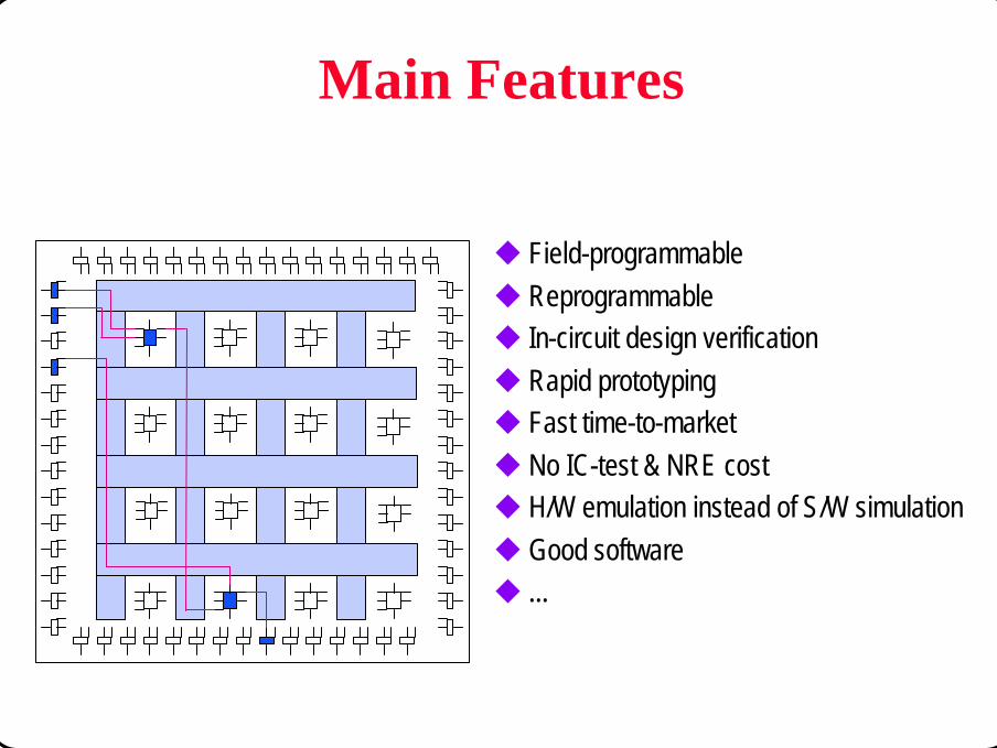
Main Features
u Field-programmableu Reprogrammableu In-circuit design verificationu Rapid prototypingu Fast time-to-marketu No IC-test & NRE costu H/W emulation instead of S/W simulationu Good softwareu ...
© CIC Altera Max+PlusII Y.T.Chou/Steven Page 5
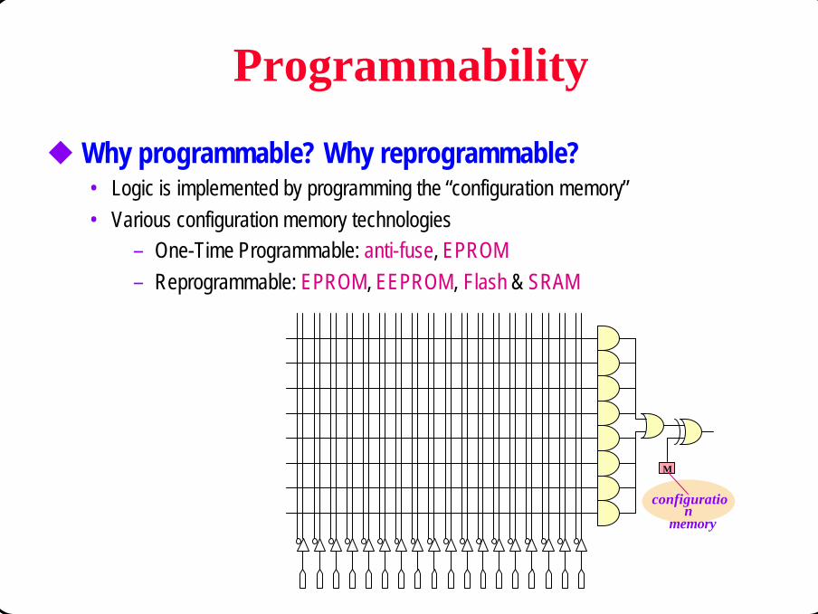
Programmability
u Why programmable? Why reprogrammable?• Logic is implemented by programming the “configuration memory”• Various configuration memory technologies
– One-Time Programmable: anti-fuse, EPROM– Reprogrammable: EPROM, EEPROM, Flash & SRAM
configuration
memory
M
© CIC Altera Max+PlusII Y.T.Chou/Steven Page 6
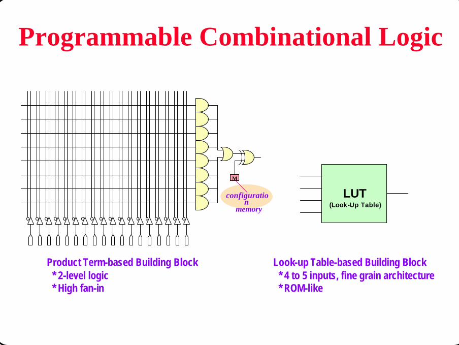
Programmable Combinational Logic
Product Term-based Building Block* 2-level logic* High fan-in
Look-up Table-based Building Block* 4 to 5 inputs, fine grain architecture* ROM-like
LUT(Look-Up Table)
configuration
memory
M

© CIC Altera Max+PlusII Y.T.Chou/Steven Page 7
Programmable Register
MM
PR
CLR
D
EN
Q
1MM
M
MM
M
MM
output select
preset select
clear select
edge control
enable select
clock select
* Typical register controls: clock, enable, preset/clear, ...

© CIC Altera Max+PlusII Y.T.Chou/Steven Page 8
Programmable Interconnect
logic block
switchingelement
switchingelement
switchingelement
switchingelement
logic cells
logic cells
logic cells
logic cells
Typical routing resources: switching elements, local/global lines, clock buffers...
© CIC Altera Max+PlusII Y.T.Chou/Steven Page 9
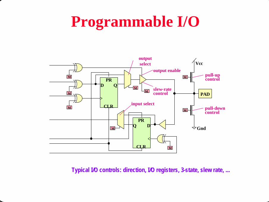
Programmable I/O
pull-downcontrol
Vcc
M
M
pull-upcontrol
PAD
Gnd
PR
CLR
D QM
M
output select
slew-ratecontrolM
output enable
M
M
M
M
PR
CLR
DQ
input select
Typical I/O controls: direction, I/O registers, 3-state, slew rate, ...
© CIC Altera Max+PlusII Y.T.Chou/Steven Page 10
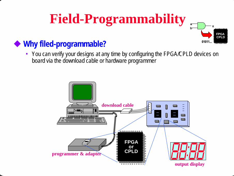
Field-Programmability
u Why filed-programmable?• You can verify your designs at any time by configuring the FPGA/CPLD devices on
board via the download cable or hardware programmer
download cable
programmer & adapter
FPGAor
CPLD
output display
FPGACPLD
ab z
01011...
© CIC Altera Max+PlusII Y.T.Chou/Steven Page 11
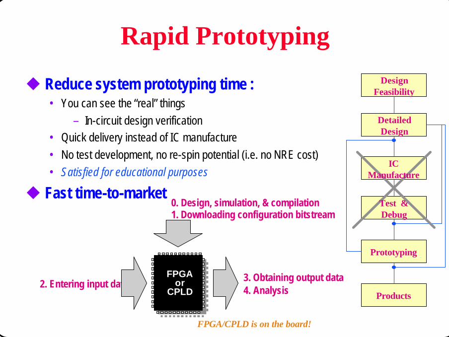
Rapid Prototyping
u Reduce system prototyping time :• You can see the “real”things
– In-circuit design verification• Quick delivery instead of IC manufacture• No test development, no re-spin potential (i.e. no NRE cost)• Satisfied for educational purposes
u Fast time-to-market
FPGAor
CPLD
0. Design, simulation, & compilation1. Downloading configuration bitstream
2. Entering input data3. Obtaining output data4. Analysis
DesignFeasibility
DetailedDesign
Prototyping
Test &Debug
ICManufacture
Products
FPGA/CPLD is on the board!
© CIC Altera Max+PlusII Y.T.Chou/Steven Page 12
Software Environment
u Various design entries and interfaces• HDL: Verilog, VHDL, ABEL, ...• Graphic: Viewlogic, OrCAD, Cadence, ...
u Primitives & macrofunctions provided• Primitive gates, arithmetic modules, flip-flops, counters, I/O elements, ...
u Constraint-driven compilation/implementation• Logic fitting, partition, placement & routing (P&R)
u Simulation netlist generation• Functional simulation & timing simulation netlist extraction
u Programmer/download program

© CIC Altera Max+PlusII Y.T.Chou/Steven Page 13
FPGA/CPLD Benefits
High-DensityPLDs
√√√
√ √
√ √√ √√ √√ √
√ √
Gate Arrays
√√√√
√
√
Cell-BasedICs
√√
√ √
√
Full-CustomICs
√ √√ √√ √
√
SpeedIntegration DensityHigh-Volume device costLow-volume device cost
Time to MarketRisk ReductionFuture ModificationDevelopment Tool
Educational Purpose
√ Good√√ Excellent

© CIC Altera Max+PlusII Y.T.Chou/Steven Page 14
Altera & CIC
u Altera• One of the world leaders in high-performance & high-density PLDs & associated
CAE tools• Supports university program in Taiwan via CIC
u From CIC, you can apply:• Altera software - it’s free for educational purpose!FPC : MAX+PLUS II (full design environment)FPC : QUARTUS II (full design environment)
• Altera hardware -• University Program Design Laboratory Package (since 9709):
• UP1/UP2 Education Board• ByteBlaster download cable• Student Edition Software
• Of course, CIC is responsible for technical supports• WWW: http://www.cic.edu.tw/chip_design/design_intr/altera/
CIC

© CIC Altera Max+PlusII Y.T.Chou/Steven Page 15
u Operate in a self-contained environment
MAX+PLUS II Can …(An Introduction)

© CIC Altera Max+PlusII Y.T.Chou/Steven Page 16
MAX+PLUS II Software Products
u Fixed-Node Subscription Products• Windows 95/98 and Windows NT Operating System, require hardware protection
key for node identification•• FIXEDPCFIXEDPC full featured MAX+PLUS II software with VHDL/Verilog
u Floating-Node Subscription Products• Licensed Using Windows NT and UNIX Servers•• FLOATPCFLOATPC for Windows 95/98 and Windows NT clients only.•• FLOATNETFLOATNET for Windows 95/98/NT and UNIX clients.
u MAX+PLUS II BASELINEBASELINE Software• entry-level version of the MAX+PLUS II software which is free of charge.
© CIC Altera Max+PlusII Y.T.Chou/Steven Page 17
MAX+PLUS II
u Supported Platforms*• PC• UNIX Platform
– Sun SPARCstation– HP 9000 Series 700/800 workstation– IBM RISC System /6000 workstation
*Please read the READ.ME file with every release of MAX+plus II
u Network licensing supported on both PC and Unix
© CIC Altera Max+PlusII Y.T.Chou/Steven Page 18
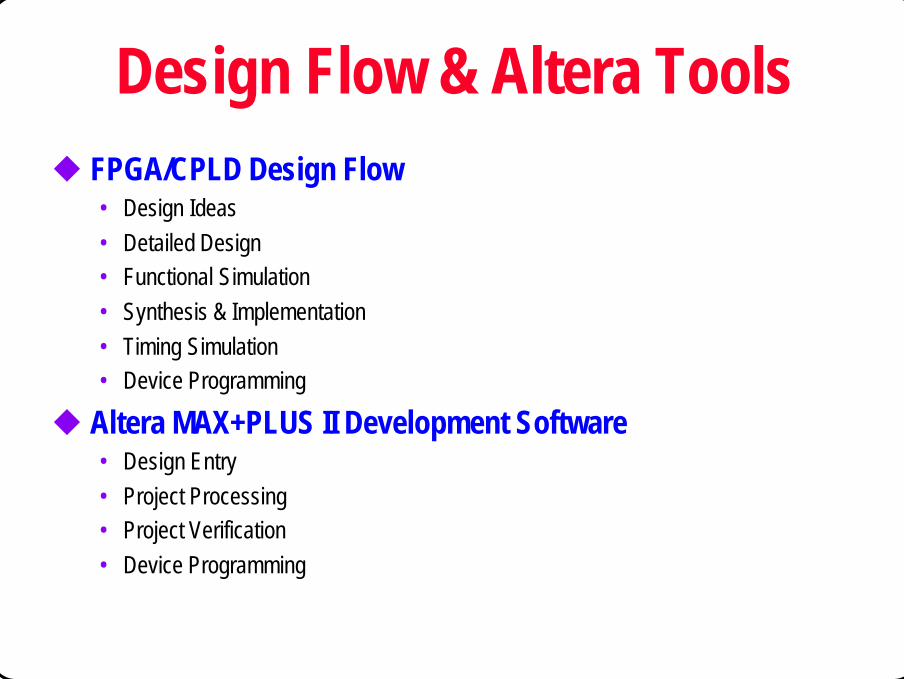
Design Flow & Altera Toolsu FPGA/CPLD Design Flow
• Design Ideas• Detailed Design• Functional Simulation• Synthesis & Implementation• Timing Simulation• Device Programming
u Altera MAX+PLUS II Development Software• Design Entry• Project Processing• Project Verification• Device Programming

© CIC Altera Max+PlusII Y.T.Chou/Steven Page 19
FPGA/CPLD Design Flow
DetailedDesign
DetailedDesign
DesignIdeas
DesignIdeas
DeviceProgramming
DeviceProgramming
TimingSimulation
TimingSimulation
Implementation(P&R)
Implementation(P&R)
FunctionalSimulation
FunctionalSimulation
tpd=22.1nsfmax=47.1MHz
FPGACPLD

© CIC Altera Max+PlusII Y.T.Chou/Steven Page 20
Design Ideas
u What are the main design considerations?• Design feasibility?• Design spec?• Cost?• FPGA/CPLD or ASIC?• Which FPGA/CPLD vendor?• Which device family?• Development time?

© CIC Altera Max+PlusII Y.T.Chou/Steven Page 21
Detailed Design
u Choose the design entry method• Schematic
– Gate level design– Intuitive & easy to debug
• HDL (Hardware Description Language), e.g. Verilog & VHDL– Descriptive & portable– Easy to modify
• Mixed HDL & schematic
u Manage the design hierarchy• Design partitioning
– Chip partitioning– Logic partitioning
• Use vendor-supplied libraries or parameterized libraries to reduce design time• Create & manage user-created libraries (circuits)

© CIC Altera Max+PlusII Y.T.Chou/Steven Page 22
Functional Simulation
u Preparation for simulation• Generate simulation patterns
– Waveform entry– HDL testbench
• Generate simulation netlist
u Functional simulation• To verify the functionality of your design only
u Simulation results• Waveform display• Text output
u Challenge• Sufficient & efficient test patterns
© CIC Altera Max+PlusII Y.T.Chou/Steven Page 23
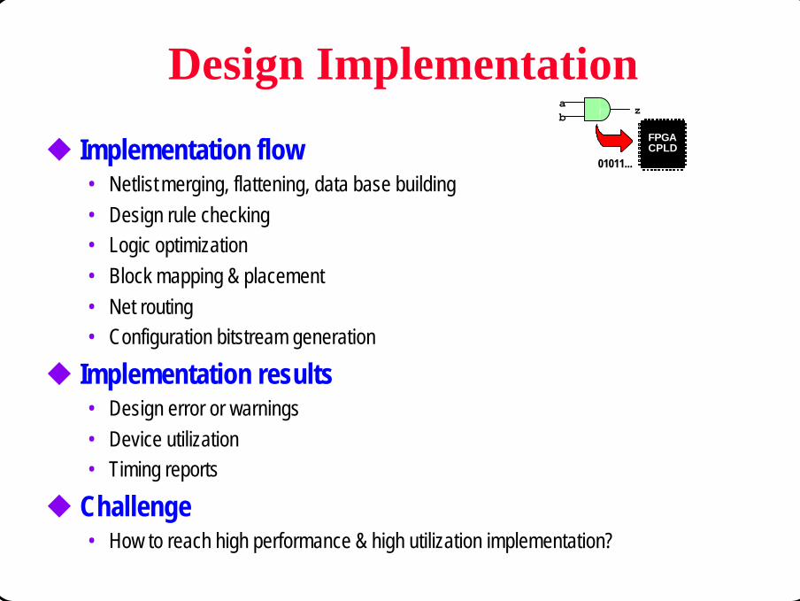
Design Implementation
u Implementation flow• Netlist merging, flattening, data base building• Design rule checking• Logic optimization• Block mapping & placement• Net routing• Configuration bitstream generation
u Implementation results• Design error or warnings• Device utilization• Timing reports
u Challenge• How to reach high performance & high utilization implementation?
FPGACPLD
ab z
01011...

© CIC Altera Max+PlusII Y.T.Chou/Steven Page 24
Timing Analysis & Simulation
u Timing analysis• Timing analysis is static, i.e., independent of input & output patterns• To examine the timing constraints• To show the detailed timing paths• Can find the critical path
u Timing simulation• To verify both the functionality & timing of the design
tpd=22.1nsfmax=47.1MHz

© CIC Altera Max+PlusII Y.T.Chou/Steven Page 25
Device Programming
u Choose the appropriate configuration scheme• SRAM-based FPGA/CPLD devices
– Downloading the bitstream via a download cable– Programming onto a non-volatile memory device & attaching it on the circuit
board• OTP, EPROM, EEPROM or Flash-based FPGA/CPLD devices
– Using hardware programmer– ISP
u Finish the board designu Program the deviceu Challenge
• Board design• System considerations
FPGACPLD

© CIC Altera Max+PlusII Y.T.Chou/Steven Page 26
Altera Design Flow
u Operate seamlessly with other EDA tools
MAX+PLUS II
Verilog HDL &VHDL Design Files
Standard EDASimulator
Verilog HDLVHDLEDIFSDF
Standard EDAHDL Files
Standard EDASchematics
EDIF
FLEXMAX
Classic

© CIC Altera Max+PlusII Y.T.Chou/Steven Page 27
MAX+PLUS IIAltera’s Fully-Integrated Development System
Project Verification
MAX+PLUS IIWaveform Editor
MAX+PLUS IISimulator
MAX+PLUS IITiming Analyzer
MAX+PLUS IISimulator
Design Entry
MAX+PLUS IIText Editor
MAX+PLUS IIFloorplan Editor
MAX+PLUS IIGraphic Editor
MAX+PLUS IISymbol Editor
MAX+PLUS IIWaveform Editor
Device Programming
MAX+PLUS IIProgrammer
Project Processing
MAX+PLUS II CompilerCNF
ExtractorDatabaseBuilder
LogicSynthesizer
SNFExtractor Partitioner Fitter
NetlistWriter
DesignDoctor Assembler
MAX+PLUS IIMessage Processor
&Hierarchy Display

© CIC Altera Max+PlusII Y.T.Chou/Steven Page 28
Design Entry
u MAX+PLUS II design entry tools• Graphic Editor & Symbol Editor
– For schematic designs• Text Editor
– For AHDL and VHDL designs– However, VHDL is not covered by this course
• Waveform Editor• Floorplan Editor• Hierarchy Display
© CIC Altera Max+PlusII Y.T.Chou/Steven Page 29
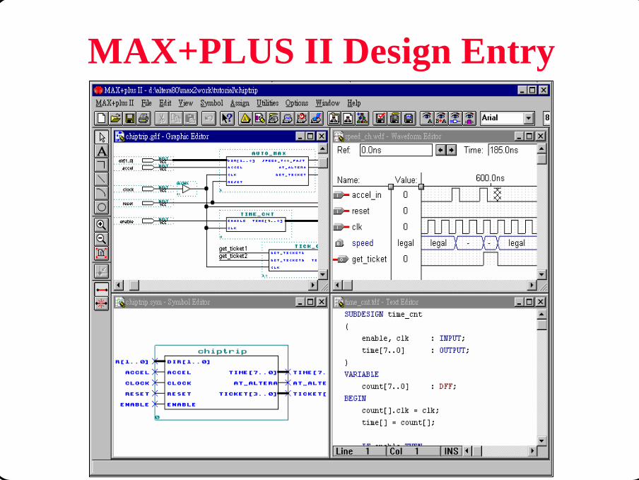
MAX+PLUS II Design Entry

© CIC Altera Max+PlusII Y.T.Chou/Steven Page 30
Project Processing
u MAX+PLUS II tools for project processing (implementation)• MAX+PLUS II Compiler• MAX+PLUS II Floorplan Editor
– For pin, logic cell location assignments• Message Processor
– For error detection & location

© CIC Altera Max+PlusII Y.T.Chou/Steven Page 31
MAX+PLUS II Project Processing

© CIC Altera Max+PlusII Y.T.Chou/Steven Page 32
Project Verification
u MAX+PLUS II tools for project verification• MAX+PLUS II Simulator• MAX+PLUS II Waveform Editor• MAX+PLUS II Timing Analyzer

© CIC Altera Max+PlusII Y.T.Chou/Steven Page 33
MAX+PLUS II Project Verification

© CIC Altera Max+PlusII Y.T.Chou/Steven Page 34
Device Programming
u MAX+PLUS tool for device programming• MAX+PLUS II Programmer

© CIC Altera Max+PlusII Y.T.Chou/Steven Page 35
MAX+PLUS II Features
u MAX+PLUS II, Altera’s fully integrated design environment• Schematic, text (AHDL), waveform design entry & hierarchy display• Floorplan editing• DRC, logic synthesis & fitting, timing-driven compilation• Multi-device partitioning• Automatic error location• Functional simulation, timing simulation, and multi-device simulation• Timing analysis• Programming file generation & device programming• EDA interface : industry-standard library support, EDA design entry & output formats
(EDIF, Verilog & VHDL)• On-line help

© CIC Altera Max+PlusII Y.T.Chou/Steven Page 36
Getting Startedu System Requirementsu Installing MAX+PLUS IIu Starting MAX+PLUS IIu Entering Authorization Codesu MAX+PLUS II Manager Windowu MAX+PLUS II Projectu Hierarchy Display

© CIC Altera Max+PlusII Y.T.Chou/Steven Page 37
System Requirements
u The minimum system requirements• Pentium- or 486-based PC• Microsoft Windows NT 3.51 or 4.0, Windows 95, or Windows version 3.1x with
Win32s support• Microsoft Windows-compatible graphics card & monitor• Microsoft Window-compatible 2- or 3-button mouse• CD-ROM drive• Parallel port
u Memory & disk space requirement• Go to the read.me file for specific information about disk space & memory
requirements in the current version of MAX+PLUS II– At least 64MB physical RAM is recommended– Memory requirement depends on the selected device and the design
complexity

© CIC Altera Max+PlusII Y.T.Chou/Steven Page 38
Installing MAX+PLUS II
u To install MAX+PLUS II from CD-ROM• Insert MAX+PLUS II CD-ROM into the CD-ROM drive. The installation program is
located at: <CD-ROM drive>:\pc\maxplus2\install.exe
• Follow the directions provided on-screen• Window 3.1x users:
– Installation program will install Win32s files if they are not already present
u Additional Windows NT installation steps• You must install Sentinel driver after running the install program
– To detect the key-pro• (Optional) ByteBlaster and Altera LP6 Logic Programmer Card drivers
– Required only for ByteBlaster or LP6 users

© CIC Altera Max+PlusII Y.T.Chou/Steven Page 39
Starting MAX+PLUS II
u To start MAX+PLUS II... • Double click on the MAX+PLUS II icon

© CIC Altera Max+PlusII Y.T.Chou/Steven Page 40
Entering the Authorization Code
u When starting MAX+PLUS II for the first timeu Options -> license setup
• You must enter an authorization code obtained from CIC • You can use all most MAX+PLUS II features after enter the correct auth-code

© CIC Altera Max+PlusII Y.T.Chou/Steven Page 41
MAX+PLUS II Operating Environmentu MAX+PLUS II Manager
• Start-up windowToolbar provides shortcuts for commonly used functions
Status bar provides a brief description of selected menu command and toolbar button
MAX+PLUS II menugives you access to all MAX+PLUS II functions
Help menu gives you access to on-line help
Project Directory andProject name
© CIC Altera Max+PlusII Y.T.Chou/Steven Page 42
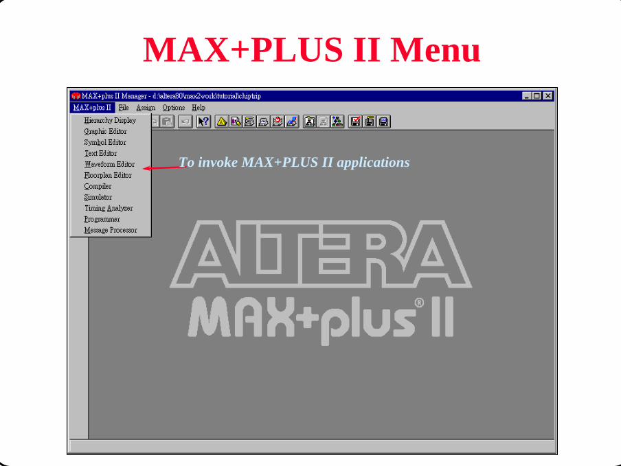
MAX+PLUS II Menu
To invoke MAX+PLUS II applications

© CIC Altera Max+PlusII Y.T.Chou/Steven Page 43
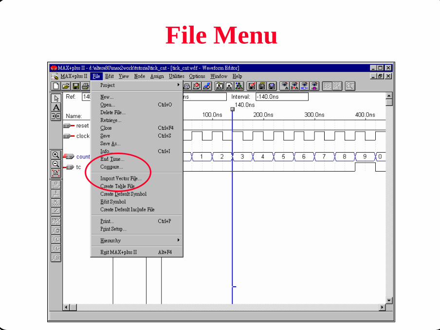
File Menu

© CIC Altera Max+PlusII Y.T.Chou/Steven Page 44
Assign Menu
To specify project assignments & options

© CIC Altera Max+PlusII Y.T.Chou/Steven Page 45
Options Menu
To setup user preferences
© CIC Altera Max+PlusII Y.T.Chou/Steven Page 46
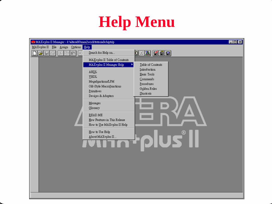
Help Menu

© CIC Altera Max+PlusII Y.T.Chou/Steven Page 47
MAX+PLUS II Help Contents
u On-line help• All of the information necessary to
enter, compile, and verify a design and to program an Altera device is available in MAX+PLUS II Help
• Help also provides introductions to all MAX+PLUS II applications, design guidelines, pin and logic cell numbers for each Altera device package

© CIC Altera Max+PlusII Y.T.Chou/Steven Page 48
MAX+PLUS IIDesign Methodology

© CIC Altera Max+PlusII Y.T.Chou/Steven Page 49
System Production
Design Specification
Design Compilation
Functional Verification
Timing Verification
Device Programming
In-System Verification
Design Modification
Design Entry
Command-LineMode

© CIC Altera Max+PlusII Y.T.Chou/Steven Page 50
Design Entry Process
u Project Setup/Managementu Multiple design entry methods
• MAX+PLUS II– Graphic design entry– Text design entry
• AHDL, VHDL, Verilog
– Waveform design entry• 3rd party EDA tools
– EDIF, OrCAD schematics• Add flexibility and optimization to the Design entry process by:
– mixing and matching design files– using LPM and Megafunctions to accelerate design entry

© CIC Altera Max+PlusII Y.T.Chou/Steven Page 51
Project Setup/Management
u What is a Project?• A design file • A project is:
– checked for design entry errors– compiled– simulated (functional or with timing)– analyzed for timing – used to generate programming file
u Projects can be archivedu To specify a project
Menu: File -> Project -> Name... (To specify an existing or new design file)
Menu: File -> Project -> Set Project to Current File (To specify the current design file)

© CIC Altera Max+PlusII Y.T.Chou/Steven Page 52
Set Up A New Projectu Every design must have a project nameu Project name must match design file name
Project Name
Project Directory

© CIC Altera Max+PlusII Y.T.Chou/Steven Page 53
Design Entry Files
MAX+PLUS IIGraphic Editor
MAX+PLUS IIText Editor
MAX+PLUS IISymbol Editor
MAX+PLUS IIFloorplan Editor
Top-Level File
.gdf
Top-level design files can be .gdf, .tdf, .vhd, .v, .sch, or .edf
.wdf .vhd .sch .edf
GraphicFile
WaveformFile
TextFile
GraphicFile
TextFile
.v
TextFile
Imported from other EDA tools
OrCAD
Synopsys,Synplicity,Mentor Graphics,etc...
Generated within MAX+PLUS II
VHDL
Waveform
Schematic
.tdf
TextFile
AHDL
Verilog

© CIC Altera Max+PlusII Y.T.Chou/Steven Page 54
Hierarchy Display
u MAX+PLUS II Hierarchy Display• The Hierarchy Display shows a hierarchy tree that represents the current hierarchy
and allows you to open and close files in the hierarchy• The hierarchy tree branches show a filename and file icon for each subdesign in the
hierarchy, and it also shows ancillary files associated with the current hierarchy.• To get a better perspective on your project, you can zoom in and out to different
display scales or switch between vertical or horizontal orientation• To invoke Hierarchy Display
Menu: MAX+PLUS II -> Hierarchy Display

© CIC Altera Max+PlusII Y.T.Chou/Steven Page 55
Hierarchy Display Window
File Icons

© CIC Altera Max+PlusII Y.T.Chou/Steven Page 56
Graphic Design Entryu MAX+PLUS II Graphic Editor & Symbol Editoru Basic Knowledge
• Naming Rules• User Libraries & System Libraries
u Creating Graphic Design Filesu Examples

© CIC Altera Max+PlusII Y.T.Chou/Steven Page 57
u Add resource libraries to search list as neededu Draw schematic
• Enter design components (symbols)• Connect components with net (wires)• Add labels to key nets signal
– Must label all busses, primary inputs,outputs,bidirNote: MAX+PLUS II DOES NOT AUTO SAVE
u Save and check the design• The file extension is .gdf• Correct any errors with the aid of Message Processor
u Create symbol or include file for sub-design
Graphic Design Entry Process

© CIC Altera Max+PlusII Y.T.Chou/Steven Page 58
Resource Librariesu prim ( Altera primitives )
• Basic logic building blocks
u mf ( Macrofunction )• 7400 family logic
u mega_lpm ( LPMs)• Library of Parameterized Modules ( LPMs )• Megafunctions are high level function module
– busmux, ram elements, fifo’s, etc...

© CIC Altera Max+PlusII Y.T.Chou/Steven Page 59
Value added Libraries
u MegaCores IP models you can try before purchase (download from www.altera.com)
– UARTs, FFT, PCI etc…
u AMPP ( Altera Megafunction Partners Program )• Partners providing PCI, DSP, µControllers, etc…
Note: For the latest information on MegaCores or Megafunctions, refer to Altera’s web site www.altera.com

© CIC Altera Max+PlusII Y.T.Chou/Steven Page 60
Add User Resource Librariesu Access user created libraries
• Add user library directories• Set priorities
Select the library directorythen click on Add
Library search priority can be changed.
The Project directory has the highest priority, followed by the User Libraries, then by the Altera Libraries

© CIC Altera Max+PlusII Y.T.Chou/Steven Page 61
Open New File & Enter Symbolsu Open a new .gdf file in Graphic Editoru Double click in Graphic file to enter symbol
Type in symbol name or click on symbol name
Symbol libraries
Symbols in the selected library
Open new file
Double click in Graphic Editor
© CIC Altera Max+PlusII Y.T.Chou/Steven Page 62
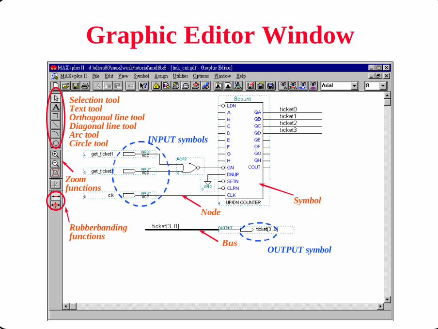
Graphic Editor Window
Selection toolText toolOrthogonal line toolDiagonal line toolArc toolCircle tool
Symbol
Bus
Node
INPUT symbols
Zoomfunctions
Rubberbandingfunctions
OUTPUT symbol

© CIC Altera Max+PlusII Y.T.Chou/Steven Page 63
Making Connections
u Wire• Single bit line
u Bus• Multi-bit line
u Signal name• Matching name• Attached to wire
Bus - Bus signal names required for LPM module buses
Wire
Wire to Bus Connection
Drawing tool shortcuts
© CIC Altera Max+PlusII Y.T.Chou/Steven Page 64
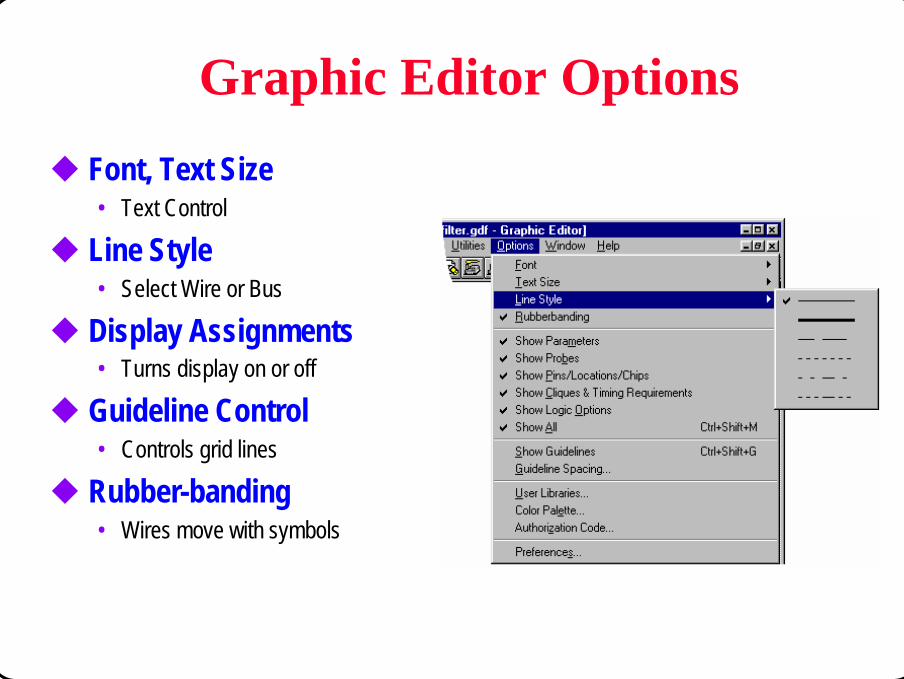
Graphic Editor Options
u Font, Text Size• Text Control
u Line Style• Select Wire or Bus
u Display Assignments• Turns display on or off
u Guideline Control• Controls grid lines
u Rubber-banding• Wires move with symbols

© CIC Altera Max+PlusII Y.T.Chou/Steven Page 65
Generate Symbols and Include Files
u Create symbol for higher-level schematic captureu Create include file for AHDL or Verilog function prototype
Create symbol
Create include file
© CIC Altera Max+PlusII Y.T.Chou/Steven Page 66
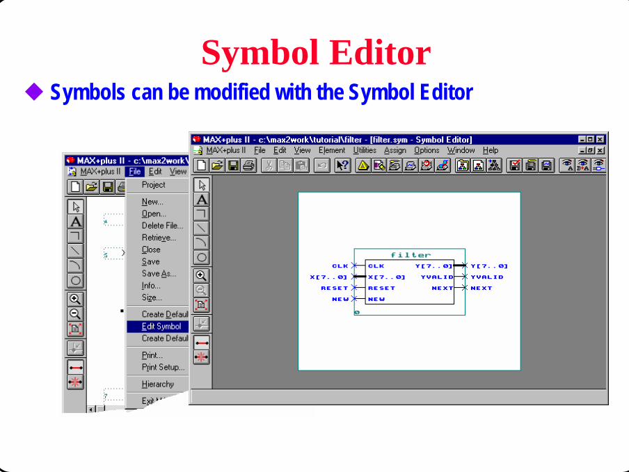
Symbol Editoru Symbols can be modified with the Symbol Editor

© CIC Altera Max+PlusII Y.T.Chou/Steven Page 67
Pin/Node Naming
u Pin/node name• A pin name is enclosed within a pin primitive symbol; a node name is a text block
that is associated with a node line (wire).
u Pin/node naming rules • It can contain up to 32 name characters• It may not contain blank spaces. Leading or trailing spaces are ignored.• It must be unique, i.e., no two pins may have the same name in the same design file
at the same hierarchy level.• Any node that is connected to a bus line must be named• Node names that are bits of a dual-range bus must be expressed in the format
<name>[<width>][<size>] or <name><width>_<size>. If you name a single node in this format, it will be interpreted as part of a dual-range bus if another single-range or dual-range bus in the file uses the same <name>.

© CIC Altera Max+PlusII Y.T.Chou/Steven Page 68
Bus Naming
u Single-range bus name• Example: D[3..0] = D3,D2,D1,D0• The bus identifier can contain up to 32 name characters; the bus width can contain
a maximum of 256 bits. The bus width is a string that defines the number of bits (i.e., nodes) in a bus and uses the form [<MSB>..<LSB>]. The name of a single node within the bus can be specified with the identifier followed by the bit number, either with or without brackets.
u Dual-range bus name• Example: D[3..0][1..0] = D3_1,D3_0,D2_1,D2_0,D1_1,D1_0• A dual-range bus name uses two bracket-enclosed ranges [ ]: the bus width and the
bus size. Bus widths and sizes can together define a maximum of 256 bits.
u Sequential bus name• Example: A[31..0],B,C[3..0]• A sequential bus name consists of a series of node names and/or bus names,
separated by commas (,). The first node or bus bit in the series is the MSB, the last node in the series is the LSB.
© CIC Altera Max+PlusII Y.T.Chou/Steven Page 69
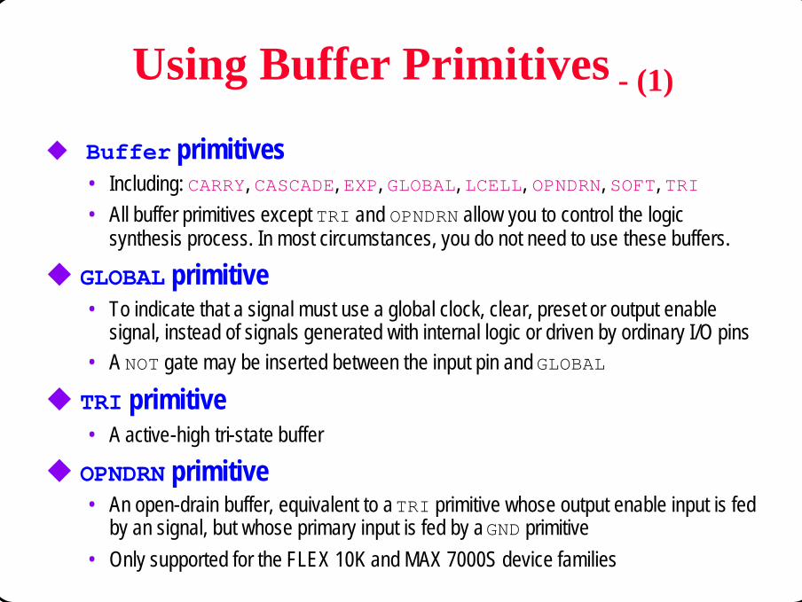
Using Buffer Primitives - (1)
u Buffer primitives• Including: CARRY, CASCADE, EXP, GLOBAL, LCELL, OPNDRN, SOFT, TRI• All buffer primitives except TRI and OPNDRN allow you to control the logic
synthesis process. In most circumstances, you do not need to use these buffers.
u GLOBAL primitive• To indicate that a signal must use a global clock, clear, preset or output enable
signal, instead of signals generated with internal logic or driven by ordinary I/O pins• A NOT gate may be inserted between the input pin and GLOBAL
u TRI primitive• A active-high tri-state buffer
u OPNDRN primitive• An open-drain buffer, equivalent to a TRI primitive whose output enable input is fed
by an signal, but whose primary input is fed by a GND primitive• Only supported for the FLEX 10K and MAX 7000S device families
© CIC Altera Max+PlusII Y.T.Chou/Steven Page 70
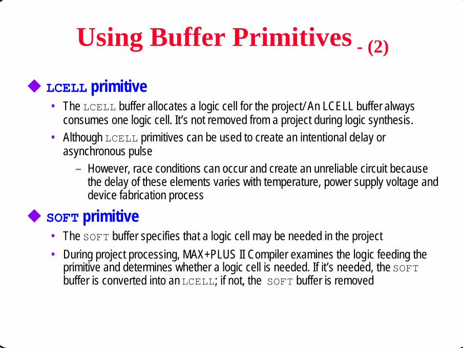
Using Buffer Primitives - (2)
u LCELL primitive• The LCELL buffer allocates a logic cell for the project/ An LCELL buffer always
consumes one logic cell. It’s not removed from a project during logic synthesis.• Although LCELL primitives can be used to create an intentional delay or
asynchronous pulse– However, race conditions can occur and create an unreliable circuit because
the delay of these elements varies with temperature, power supply voltage and device fabrication process
u SOFT primitive• The SOFT buffer specifies that a logic cell may be needed in the project• During project processing, MAX+PLUS II Compiler examines the logic feeding the
primitive and determines whether a logic cell is needed. If it’s needed, the SOFTbuffer is converted into an LCELL; if not, the SOFT buffer is removed

© CIC Altera Max+PlusII Y.T.Chou/Steven Page 71
More on LPM Libraries
u Library of Parameterized Modules• Standard Library of basic and functional elements• Based on EDIF standard
u Advantage of LPMs• Portability of design• Architecture independence
u MAX+PLUS II and LPMs• LPM can be used in graphical design and HDL designs• LPM can be customized via the Megawizard feature

© CIC Altera Max+PlusII Y.T.Chou/Steven Page 72
Standard LPM without Megawizard
© CIC Altera Max+PlusII Y.T.Chou/Steven Page 73
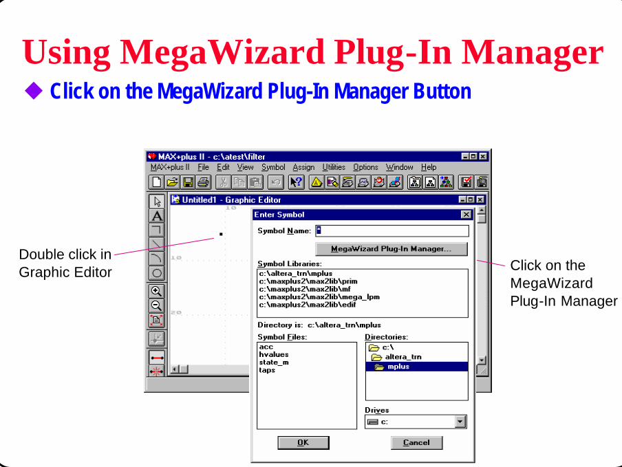
Using MegaWizard Plug-In Manageru Click on the MegaWizard Plug-In Manager Button
Click on the MegaWizardPlug-In Manager
Double click in Graphic Editor

© CIC Altera Max+PlusII Y.T.Chou/Steven Page 74
Accessing the MegaWizard
Select MegaWizard Plug-In Manager

© CIC Altera Max+PlusII Y.T.Chou/Steven Page 75
New vs Existing Megafunctionu Choose between a new custom megafunction variation or an
existing megafunction variation
New Custom Megafunction
Edit Existing Custom Megafunction

© CIC Altera Max+PlusII Y.T.Chou/Steven Page 76
Available Megafunctions & Output File
Select a functionfrom the availablemegafunction Select a type
of
output file
Select a directoryand a output filename
© CIC Altera Max+PlusII Y.T.Chou/Steven Page 77
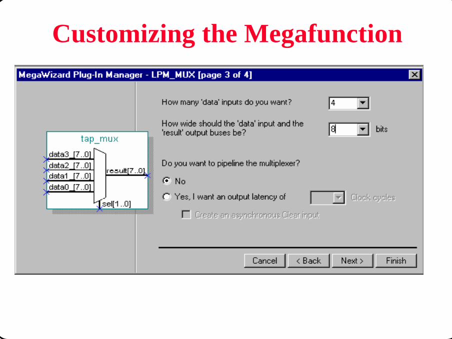
Customizing the Megafunction
© CIC Altera Max+PlusII Y.T.Chou/Steven Page 78
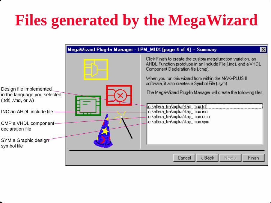
Files generated by the MegaWizard
Design file implemented in the language you selected(.tdf, .vhd, or .v)
INC an AHDL include file
CMP a VHDL componentdeclaration file
SYM a Graphic designsymbol file

© CIC Altera Max+PlusII Y.T.Chou/Steven Page 79
Entering Customized Megafunction
Customized megafunction appearsthe same way as other symbols in the Enter symbol window
Double click in Graphic Editor
© CIC Altera Max+PlusII Y.T.Chou/Steven Page 80
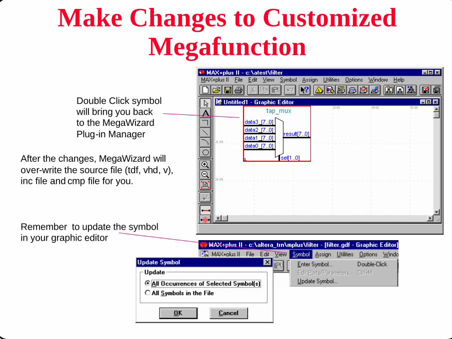
Make Changes to Customized Megafunction
After the changes, MegaWizard will over-write the source file (tdf, vhd, v),inc file and cmp file for you.
Double Click symbolwill bring you backto the MegaWizardPlug-in Manager
Remember to update the symbol in your graphic editor
© CIC Altera Max+PlusII Y.T.Chou/Steven Page 81
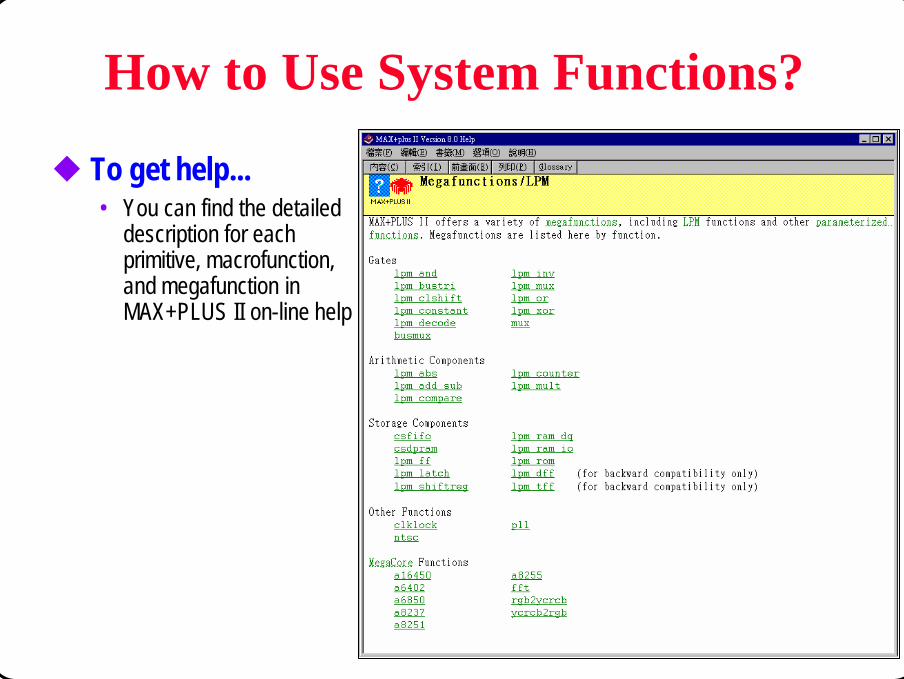
How to Use System Functions?
u To get help...• You can find the detailed
description for each primitive, macrofunction, and megafunction in MAX+PLUS II on-line help

© CIC Altera Max+PlusII Y.T.Chou/Steven Page 82
Entering Symbols
u Enter a symbolMenu: Symbol -> Enter Symbol...(or by double clicking on the empty workspace)
u Move/cut/copy/paste symbols• You can move, cut, copy or paste symbols in the
same way as you did in another Windows-based software
– Move: click & drag (mouse)– Cut: Ctrl-X– Copy: Ctrl-C or Ctrl-Click & drag– Paste: Ctrl-V– Undo: Ctrl-Z
u Commands regarding the symbol• Just click the right mouse button on the symbol

© CIC Altera Max+PlusII Y.T.Chou/Steven Page 83
Entering I/O Symbol
u I/O symbols• Input pin/port: enter a INPUT symbol• Output pin/port: enter a OUTPUT symbol• Bidirectional pin/port: enter a BIDIR symbol
u Name the I/O pins/ports• Double click on the “PIN_NAME”field of the I/O symbol
u Pin default value• The values assigned to unconnected INPUT and BIDIR primitives when the symbol
that represents the current GDF file is used in a higher-level design file• Default is VCC • Double click on the
“VCC”field to setthe default value

© CIC Altera Max+PlusII Y.T.Chou/Steven Page 84
Save & Check the Designn Save & check the design file with .gdf extensionn Correct any errors with the aid of Message Processor
Design File Name
Project Directory

© CIC Altera Max+PlusII Y.T.Chou/Steven Page 85
Message Processorn Lists all Info, Warning and Error messages
– Info messages are general information– Warning messages are possible problems– Error messages indicate Compiler is unable to complete
compilation process
n Provides help on the messagesn Locates source of message in design file
Messages
Go to next or previous message
Information about message
Locate source in design file
© CIC Altera Max+PlusII Y.T.Chou/Steven Page 86
Example: Multiplier
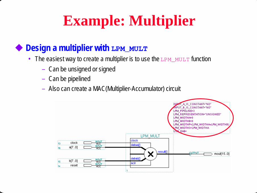
u Design a multiplier with LPM_MULT• The easiest way to create a multiplier is to use the LPM_MULT function
– Can be unsigned or signed– Can be pipelined– Also can create a MAC(Multiplier-Accumulator) circuit
© CIC Altera Max+PlusII Y.T.Chou/Steven Page 87
Example: Multiplexer
u Design a multiplexer with LPM_MUX• Use WIRE primitive to rename
a bus or node• LPM_MUX data input is a dual
range bus

© CIC Altera Max+PlusII Y.T.Chou/Steven Page 88
Example: RAM
u Design RAM circuit with LPM• Use LPM_RAM_IO to design RAM with a single input & output port• Use LPM_RAM_DQ to design RAM with separate input & output ports
© CIC Altera Max+PlusII Y.T.Chou/Steven Page 89
Example: Sequencer
u Design a sequencer with LPM_COUNTER & LPM_ROM• ROM data is specified in a Memory Initialization File (.mif) or a Intel-Hex File (.hex)• This example only sequences through 19 states so the modulus of lpm_counter is
set to 19. It uses a small section of an EAB (19 out of 256-address locations)

© CIC Altera Max+PlusII Y.T.Chou/Steven Page 90
Example: Bidirectional Pin
u Use TRI & BIDIR pin symbol• If the TRI symbol feeds to a output or bidirectional pin, it will be implemented as tri-
state buffer in the I/O cell
© CIC Altera Max+PlusII Y.T.Chou/Steven Page 91
Example: Tri-State Buses - (1)
u Tri-state emulation• Altera devices do not have internal tri-state buses• MAX+PLUS II can emulate tri-state buses by using multiplexers and by routing the
bidirectional line outside of the device and then back in through another pin
MAX+PLUS II will automatically convert it into a multiplexer.If the tri-state buffers feed a pin, a tri-state buffer will be availableafter the multiplexer.

© CIC Altera Max+PlusII Y.T.Chou/Steven Page 92
Example: Tri-State Buses - (2)
u Tri-state buses for bidirectional communication• When tri-state buses are used to multiplex signals, MAX+PLUS II will convert the
logic to a combinatorial multiplexer• When tri-state buses are used for bidirectional communication, you can rout this
bidirectional line outside of the device, which uses the tri-states present at the I/O pins, or you can convert the tri-state bus into a multiplexer
© CIC Altera Max+PlusII Y.T.Chou/Steven Page 93
Example: Tri-State Buses - (3)
Rout this bidirectional line outside of the device
Tri-state emulation
© CIC Altera Max+PlusII Y.T.Chou/Steven Page 94
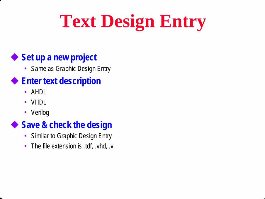
u Set up a new project• Same as Graphic Design Entry
u Enter text description• AHDL• VHDL• Verilog
u Save & check the design• Similar to Graphic Design Entry• The file extension is .tdf, .vhd, .v
Text Design Entry

© CIC Altera Max+PlusII Y.T.Chou/Steven Page 95
AHDL
u Altera Hardware Description Languageu High-level hardware behavior description languageu Uses Boolean equations, arithmetic operators, truth tables,
conditional statements, etc.u Especially well-suited for large or complex state machinesu Text Editor has AHDL Template and Syntax Coloru Refer to the Appendix for more info on AHDL
© CIC Altera Max+PlusII Y.T.Chou/Steven Page 96
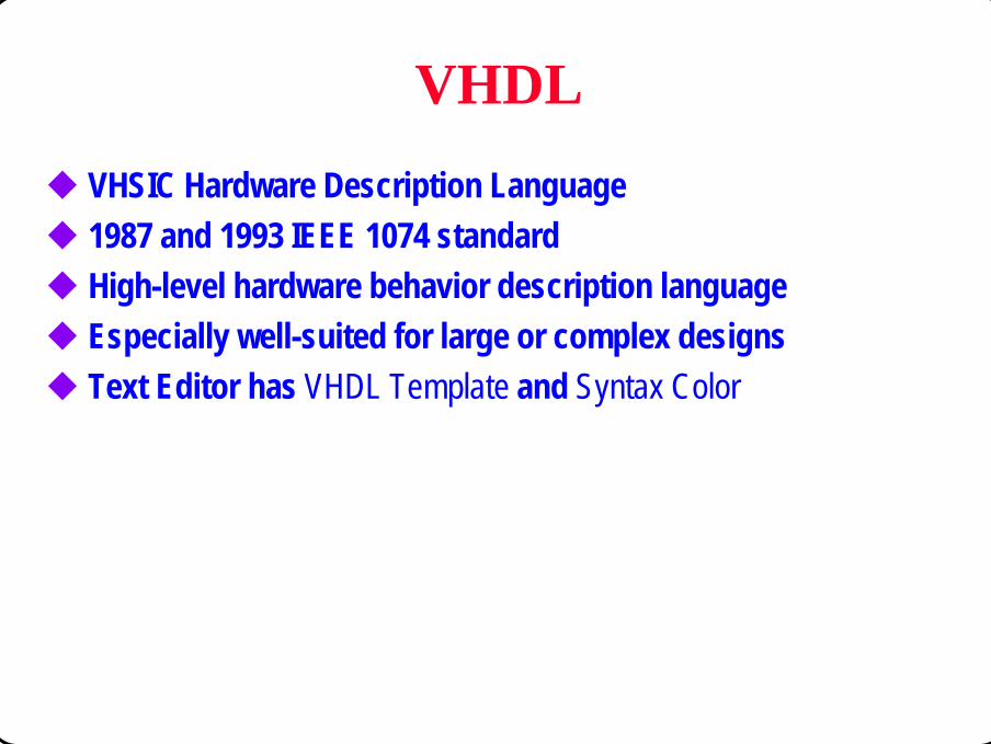
VHDL
u VHSIC Hardware Description Languageu 1987 and 1993 IEEE 1074 standardu High-level hardware behavior description languageu Especially well-suited for large or complex designsu Text Editor has VHDL Template and Syntax Color

© CIC Altera Max+PlusII Y.T.Chou/Steven Page 97
Verilog
u Hardware Description Languageu 1993 Verilog IEEE 1364 standardu High-level hardware behavior description languageu Especially well-suited for large or complex designsu Text Editor has Verilog Template and Syntax Color
© CIC Altera Max+PlusII Y.T.Chou/Steven Page 98
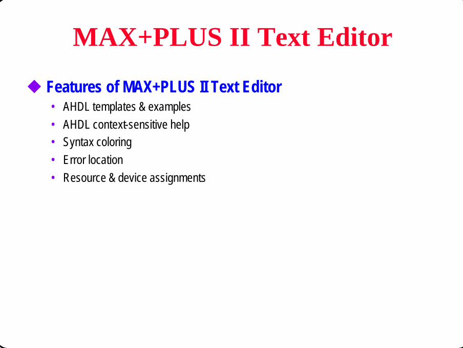
MAX+PLUS II Text Editor
u Features of MAX+PLUS II Text Editor• AHDL templates & examples• AHDL context-sensitive help• Syntax coloring• Error location• Resource & device assignments

© CIC Altera Max+PlusII Y.T.Chou/Steven Page 99
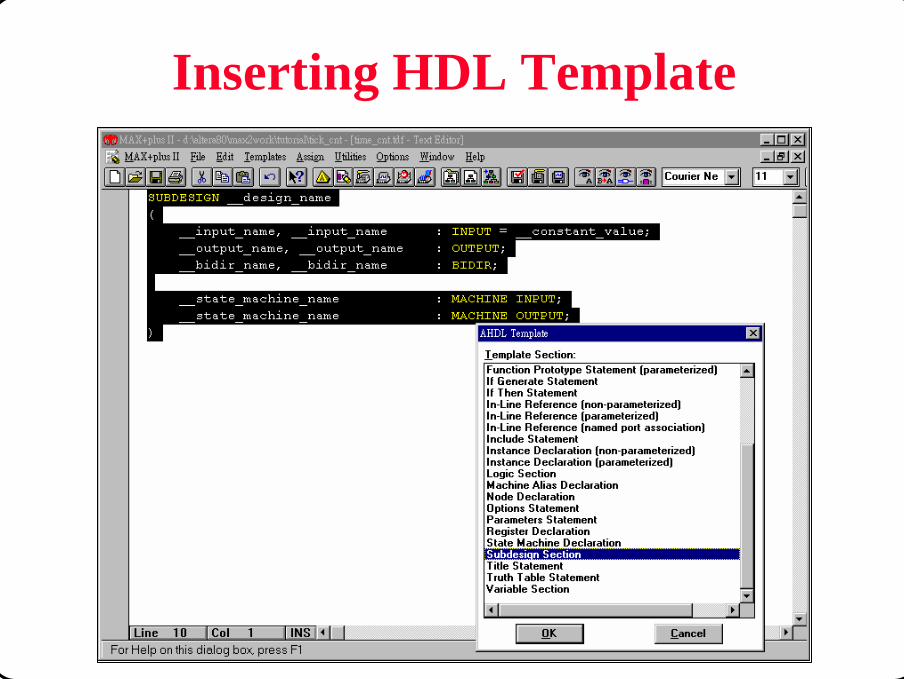
HDL Templates
u HDL templates make design easier• You can insert HDL template into your TDF, then replace placeholder variables in
the templates with your own identifiers and expressionsMenu: Templates -> HDL Template...
© CIC Altera Max+PlusII Y.T.Chou/Steven Page 100
Inserting HDL Template

© CIC Altera Max+PlusII Y.T.Chou/Steven Page 101
Using Syntax Coloring
u Syntax Coloring command• To improve TDF readability & accuracy
Menu: Options -> Syntax Coloring
u To customize the color paletteMenu: Options -> Color Palette...
• The HDL-relative options:– Comments– Illegal Characters– Megafunctions/Macrofunctions– Reserved Identifiers– Reserved Keywords– Strings– Text

© CIC Altera Max+PlusII Y.T.Chou/Steven Page 102
Text Editor with Syntax Coloring
© CIC Altera Max+PlusII Y.T.Chou/Steven Page 103
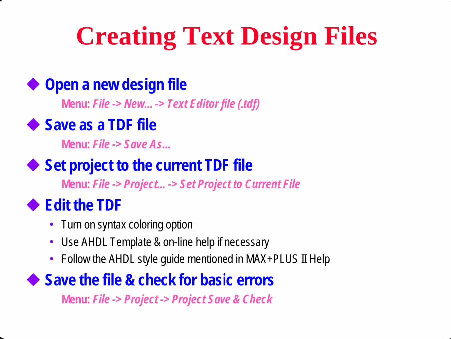
Creating Text Design Files
u Open a new design fileMenu: File -> New... -> Text Editor file (.tdf)
u Save as a TDF fileMenu: File -> Save As...
u Set project to the current TDF file Menu: File -> Project... -> Set Project to Current File
u Edit the TDF• Turn on syntax coloring option• Use AHDL Template & on-line help if necessary• Follow the AHDL style guide mentioned in MAX+PLUS II Help
u Save the file & check for basic errorsMenu: File -> Project -> Project Save & Check

© CIC Altera Max+PlusII Y.T.Chou/Steven Page 104
Example: Decoder
u Design a decoder with...• If-Then statements• Case statements• Table statements• LPM function: LPM_DECODE
SUBDESIGN decoder(
code[1..0] : INPUT;out[3..0] : OUTPUT;
)
BEGINCASE code[] ISWHEN 0 => out[] = B"0001";WHEN 1 => out[] = B"0010";WHEN 2 => out[] = B"0100";WHEN 3 => out[] = B"1000";
END CASE;END;
SUBDESIGN priority(
low, middle, high : INPUT;highest_level[1..0] : OUTPUT;
)BEGIN
IF high THENhighest_level[] = 3;ELSIF middle THENhighest_level[] = 2;
ELSIF low THENhighest_level[] = 1;
ELSEhighest_level[] = 0;
END IF;END;
© CIC Altera Max+PlusII Y.T.Chou/Steven Page 105
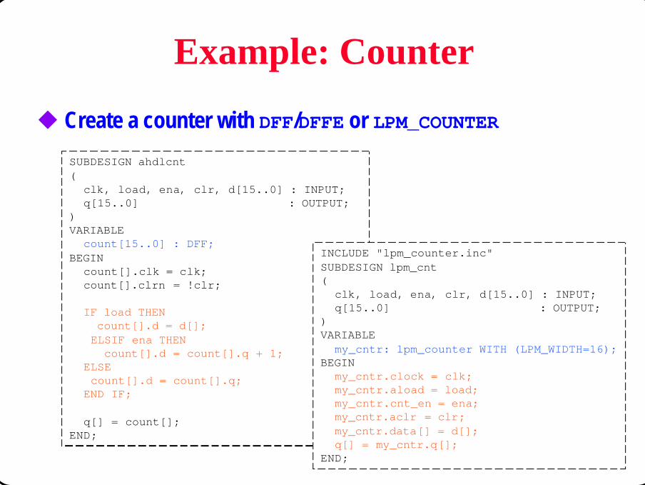
Example: Counter
u Create a counter with DFF/DFFE or LPM_COUNTER
SUBDESIGN ahdlcnt(
clk, load, ena, clr, d[15..0] : INPUT;q[15..0] : OUTPUT;
)VARIABLE
count[15..0] : DFF;BEGIN
count[].clk = clk;count[].clrn = !clr;
IF load THENcount[].d = d[];ELSIF ena THENcount[].d = count[].q + 1;
ELSEcount[].d = count[].q;
END IF;
q[] = count[];END;
INCLUDE "lpm_counter.inc"SUBDESIGN lpm_cnt(
clk, load, ena, clr, d[15..0] : INPUT;q[15..0] : OUTPUT;
)VARIABLE
my_cntr: lpm_counter WITH (LPM_WIDTH=16);BEGIN
my_cntr.clock = clk;my_cntr.aload = load;my_cntr.cnt_en = ena;my_cntr.aclr = clr;my_cntr.data[] = d[];q[] = my_cntr.q[];
END;

© CIC Altera Max+PlusII Y.T.Chou/Steven Page 106
Example: Multiplier
u Design a multiplier with LPM_MULT
CONSTANT WIDTH = 4;INCLUDE "lpm_mult.inc";
SUBDESIGN tmul3t(a[WIDTH-1..0] : INPUT;b[WIDTH-1..0] : INPUT;out[2*WIDTH-1..0] : OUTPUT;)
VARIABLEmult : lpm_mult WITH (LPM_REPRESENTATION="SIGNED",
LPM_WIDTHA=WIDTH, LPM_WIDTHB=WIDTH,LPM_WIDTHS=WIDTH, LPM_WIDTHP=WIDTH*2);
BEGINmult.dataa[] = a[];mult.datab[] = b[];out[] = mult.result[];
END;

© CIC Altera Max+PlusII Y.T.Chou/Steven Page 107
Example: Multiplexer
u Design a multiplexer with LPM_MUX
FUNCTION lpm_mux (data[LPM_SIZE-1..0][LPM_WIDTH-1..0], sel[LPM_WIDTHS-1..0]) WITH (LPM_WIDTH, LPM_SIZE, LPM_WIDTHS, CASCADE_CHAIN)RETURNS (result[LPM_WIDTH-1..0]);
SUBDESIGN mux(
a[3..0], b[3..0], c[3..0], d[3..0] : INPUT;select[1..0] : INPUT;result[3..0] : OUTPUT;
)
BEGINresult[3..0] = lpm_mux (a[3..0], b[3..0], c[3..0], d[3..0], select[1..0])WITH (LPM_WIDTH=4, LPM_SIZE=4, LPM_WIDTHS=2);
END;

© CIC Altera Max+PlusII Y.T.Chou/Steven Page 108
Example: RAM
u Design RAM circuit with LPM
INCLUDE "lpm_ram_dq.inc";
SUBDESIGN ram_dq(
clk : INPUT;we : INPUT;ram_data[31..0] : INPUT;ram_add[7..0] : INPUT;data_out[31..0] : OUTPUT;
)
BEGIN
data_out[31..0] = lpm_ram_dq (ram_data[31..0], ram_add[7..0], we, clk, clk)WITH (LPM_WIDTH=32, LPM_WIDTHAD=8);
END;

© CIC Altera Max+PlusII Y.T.Chou/Steven Page 109
Example: Tri-State Buses
u Design tri-state buses with TRI
SUBDESIGN tribus(
ina[7..0], inb[7..0], inc[7..0], oe_a, oe_b, oe_c, clock : INPUT;out[7..0] : OUTPUT;
)
VARIABLEflip[7..0] : DFF; tri_a[7..0], tri_b[7..0], tri_c[7..0] : TRI;mid[7..0] : TRI_STATE_NODE;
BEGIN-- Declare the data inputs to the tri-state buses
tri_a[] = ina[]; tri_b[] = inb[]; tri_c[] = inc[];-- Declare the output enable inputs to the tri-state buses
tri_a[].oe = oe_a; tri_b[].oe = oe_b; tri_c[].oe = oe_c;-- Connect the outputs of the tri-state buses together
mid[] = tri_a[]; mid[] = tri_b[]; mid[] = tri_c[];-- Feed the output pins
flip[].d = mid[]; flip[].clk = clock; out[] = flip[].q;END;
© CIC Altera Max+PlusII Y.T.Chou/Steven Page 110
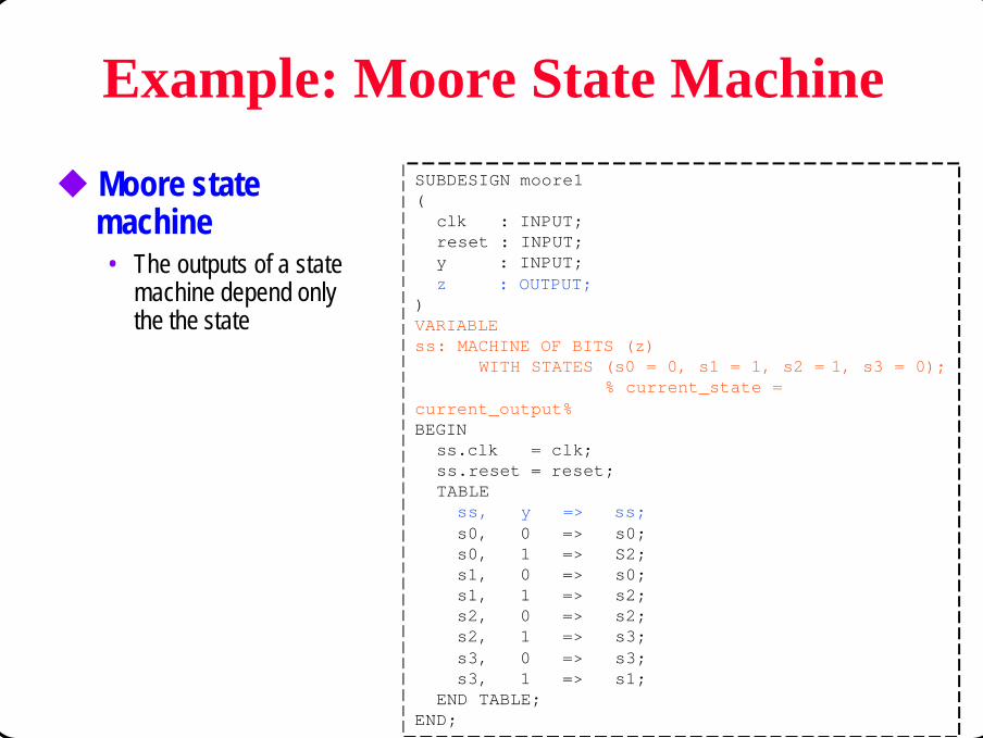
Example: Moore State Machine
u Moore state machine
• The outputs of a state machine depend only the the state
SUBDESIGN moore1(
clk : INPUT;reset : INPUT;y : INPUT;z : OUTPUT;
)VARIABLEss: MACHINE OF BITS (z)
WITH STATES (s0 = 0, s1 = 1, s2 = 1, s3 = 0);% current_state =
current_output%BEGIN
ss.clk = clk;ss.reset = reset;TABLEss, y => ss;s0, 0 => s0;s0, 1 => S2;s1, 0 => s0;s1, 1 => s2;s2, 0 => s2;s2, 1 => s3;s3, 0 => s3;s3, 1 => s1;
END TABLE;END;

© CIC Altera Max+PlusII Y.T.Chou/Steven Page 111
Example: Mealy State Machine
u Mealy state machine• A state machine with
asynchronous output(s)
SUBDESIGN mealy(
clk : INPUT;reset : INPUT;y : INPUT;z : OUTPUT;
)VARIABLE
ss: MACHINE WITH STATES (s0, s1, s2, s3);BEGIN
ss.clk = clk;ss.reset = reset;TABLEss, y => z, ss;s0, 0 => 0, s0;s0, 1 => 1, s1;s1, 0 => 1, s1;s1, 1 => 0, s2;s2, 0 => 0, s2;s2, 1 => 1, s3;s3, 0 => 0, s3;s3, 1 => 1, s0;
END TABLE;END;

© CIC Altera Max+PlusII Y.T.Chou/Steven Page 112
Waveform Design Entryu MAX+PLUS II Waveform Editoru Creating Waveform Filesu ExamplesuDesign Entry Summary

© CIC Altera Max+PlusII Y.T.Chou/Steven Page 113
MAX+PLUS II Waveform Editor
u Features of MAX+PLUS II Waveform Editor• To serve 2 roles:
– As a design entry tool: to create Altera waveform design files (*.wdf)– As a tool for entering test vectors & viewing simulation results: simulation
channel files (*.scf)
u For design entry• Waveform design entry is best suited for circuits with well-defined sequential inputs
& outputs, such as state machines, counters, and registers
u For design verification• Waveform Editor is a simulation pattern editor/viewer• Waveform Editor is fully integrated with MAX+PLUS II Simulator & Programmer to
provide full project verification flow

© CIC Altera Max+PlusII Y.T.Chou/Steven Page 114
MAX+PLUS IIWaveform Design Environment
Pop-up menu(clicking mouse B2/B3)
Zoomfunctions
Waveformvaluesoverwritingfunctions
© CIC Altera Max+PlusII Y.T.Chou/Steven Page 115
File Menu

© CIC Altera Max+PlusII Y.T.Chou/Steven Page 116
Node Menu
To enter the node or group information
© CIC Altera Max+PlusII Y.T.Chou/Steven Page 117
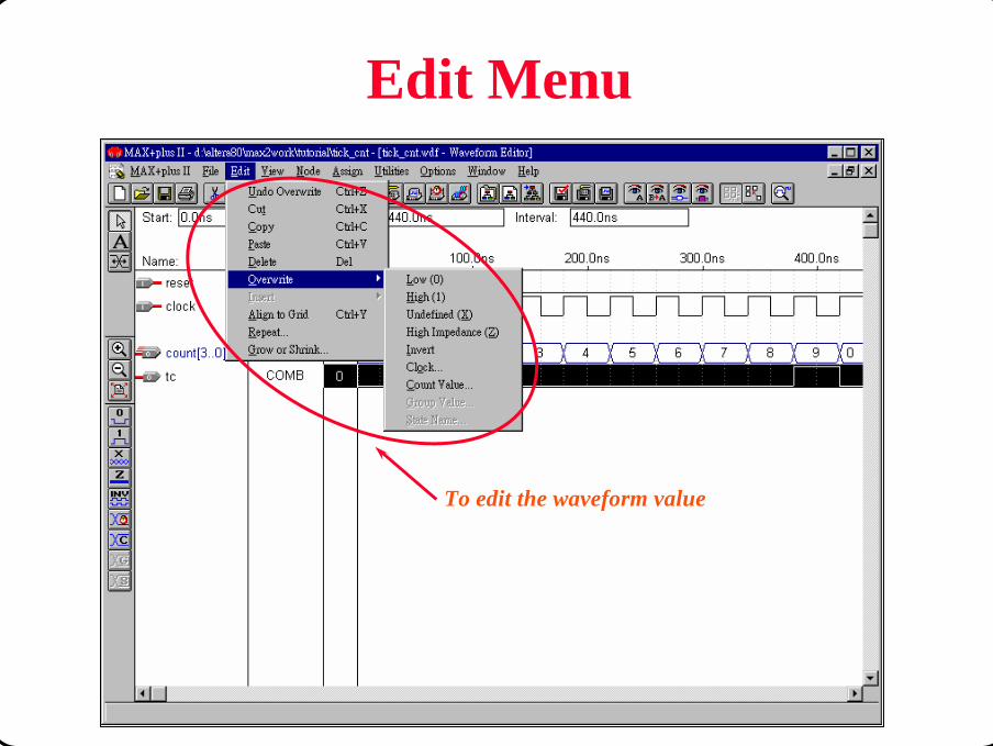
Edit Menu
To edit the waveform value

© CIC Altera Max+PlusII Y.T.Chou/Steven Page 118
Creating a New Waveform File
u Open a new design fileMenu: File -> New... -> Waveform Editor file (.wdf or .scf)
u Save as a WDF / SCF fileMenu: File -> Save As... ->
u Set project to current file (for WDF file only)Menu: File -> Project... -> Set Project to Current File

© CIC Altera Max+PlusII Y.T.Chou/Steven Page 119
u Set the grid size & show the gridMenu: Options -> Grid Size...Menu: Options -> Show Grid
• Setting appropriate grid size is helpful for waveform repeating & overwriting count value operations
u Specify the end timeMenu: File -> End Time...
u Regarding the grid size & interval...• In a WDF, the grid size & interval are arbitrary. The time scale indicates only a
sequential order of operations, not a specific response time.• In a SCF, the grid size & interval are important for timing simulation. MAX+PLUS II
Simulator reflects the real-world timing according to your SCF and the specific device. Setup & Hold time violation will occur if you enter impractical simulation patterns.
Setting Waveform Editor Options

© CIC Altera Max+PlusII Y.T.Chou/Steven Page 120
Entering Nodes
u Insert the node or group for WDF fileMenu: Node -> Insert Node... (or double click on the node name field)
• You can specify the node name, I/O type, node type & default value– Registered & machine node type must specify a clock signal and optionally
specify reset or preset signal (active high)– You can specify machine values with the state names instead of logic values

© CIC Altera Max+PlusII Y.T.Chou/Steven Page 121
Entering Nodes from SNF
u Enter the node or group for SCF fileMenu: Node -> Enter Nodes from SNF...
• SNF: Simulation Netlist File– Generated by MAX+PLUS II Compiler (discussed later)– After compilation, you can list the nodes and help you to create the SCF file

© CIC Altera Max+PlusII Y.T.Chou/Steven Page 122
Editing Waveforms - (1)
u Edit the waveforms• First select the interval to edit
– Sometimes you may specify new grid size for easy selection• To create clock-like waveform
Menu: Edit -> Overwrite -> Clock...• To edit the state machine node values
Menu: Edit -> Overwrite State Name...

© CIC Altera Max+PlusII Y.T.Chou/Steven Page 123
Editing Waveforms - (2)
u Edit the waveforms• To edit the node values
Menu: Edit -> Overwrite -> 0 / 1 / X / Z / Invert / Count Value / Group Value• To stretch / compress the selected signal
Menu: Edit -> Grow or Shrink...
• To align node values or state names to grid if necessaryMenu: Edit -> Align to Grid
© CIC Altera Max+PlusII Y.T.Chou/Steven Page 124
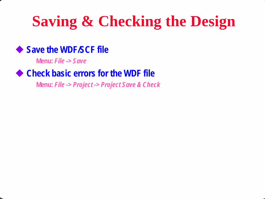
Saving & Checking the Design
u Save the WDF/SCF fileMenu: File -> Save
u Check basic errors for the WDF fileMenu: File -> Project -> Project Save & Check

© CIC Altera Max+PlusII Y.T.Chou/Steven Page 125
Waveform File Formats
u MAX+PLUS II file formats• Binary format: WDF & SCF files• ASCII format (Altera vector file format): TBL & VEC files
– TBL: an ASCII-format table file that records all logic level transitions for nodes and groups in the current SCF or WDF
– VEC: an ASCII text file used as the input for simulation, functional testing, or waveform design entry
– Refer to MAX+PLUS II Help for detailed information about vector file format
u To create a table file (*.tbl)Menu: File -> Create Table File...
u To import a vector file (*.vec)Menu: File -> Import Vector File...

© CIC Altera Max+PlusII Y.T.Chou/Steven Page 126
WDF Design Guidelines
u When design a WDF file...• WDFs cannot be at intermediate levels of a hierarchy• Include all possible combinations of input values• Align all logic level and state name transition• Assume a 0ns propagation delay for all logic• Assume a 0.1ns setup time and 0ns hold time for state machine node• For clarity, Altera recommends that you draw inputs that affect registers only on
falling clock edges• If a function is cyclical, show the last set of conditions looping back to the first by
repeating the first time-slice at the end of the cycle
© CIC Altera Max+PlusII Y.T.Chou/Steven Page 127
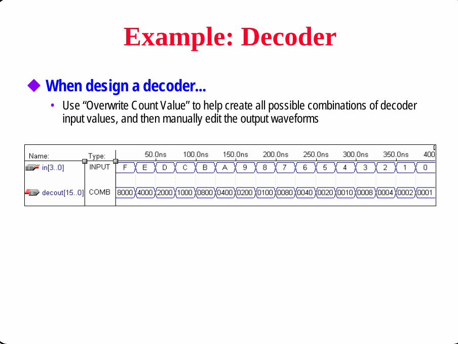
Example: Decoder
u When design a decoder...• Use “Overwrite Count Value”to help create all possible combinations of decoder
input values, and then manually edit the output waveforms

© CIC Altera Max+PlusII Y.T.Chou/Steven Page 128
Example: Counter
u When design a counter• Use “Overwrite Count Value”command to create a regular counter waveform

© CIC Altera Max+PlusII Y.T.Chou/Steven Page 129
Example: State Machine
u When design a state machine• Use “Overwrite State Name”to help create a state machine output
– You can specify machine values with the state names instead of logic values • Make sure all possible combinations of inputs and states are included

© CIC Altera Max+PlusII Y.T.Chou/Steven Page 130
DesignFiles
SupportFiles
Design Entry Summary
MAX+PLUS IIGraphic Editor
MAX+PLUS IIText Editor
MAX+PLUS IISymbol Editor
MAX+PLUS IIWaveform Editor
.gdf
.tdf
.vhd
.sch
.edf
MAX+PLUS II
3rd Party EDATools
.sym
.inc
User.wdf
.lmf
.v

© CIC Altera Max+PlusII Y.T.Chou/Steven Page 131
Design Implementationu MAX+PLUS II Compileru Preparing for Compilationu Compiling the Projectu Analyzing the Compilation Resultsu Floorplan Editoru Appendix: Interfacing with 3rd-Party Tools

© CIC Altera Max+PlusII Y.T.Chou/Steven Page 132
System Production
Design Specification
Design Entry
Simulation
Device Programming
In-System Verification
Design Modification
Compilation
Timing Analysis
Command-LineMode
© CIC Altera Max+PlusII Y.T.Chou/Steven Page 133
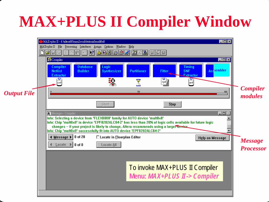
MAX+PLUS II Compiler Window
Compilermodules
MessageProcessor
To invoke MAX+PLUS II CompilerMenu: MAX+PLUS II -> Compiler
Output File

© CIC Altera Max+PlusII Y.T.Chou/Steven Page 134
MAX+PLUS II Compiler
uProcess all design files associated with the project• Files can be created with MAX+PLUS II or 3rd party EDA Tools
uChecks for syntax errors and common design pitfallsuPerforms logic synthesis and place & route
• According to assignments in .acf file
uGenerates files for simulation and timing analysis• Files can be used by MAX+PLUS II or 3rd party EDA Tools
uGenerates files for programming targeted devices
© CIC Altera Max+PlusII Y.T.Chou/Steven Page 135
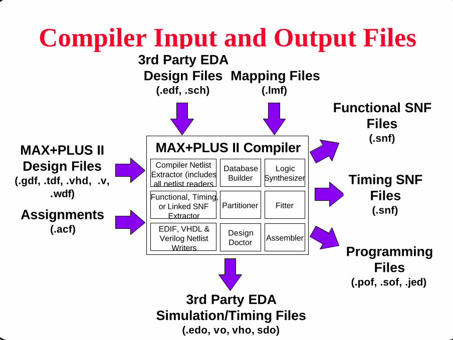
Compiler Input and Output Files
MAX+PLUS IIDesign Files
(.gdf, .tdf, .vhd, .v, .wdf)
MAX+PLUS II CompilerCompiler Netlist
Extractor (includesall netlist readers
Functional, Timing,or Linked SNF
Extractor
EDIF, VHDL &Verilog Netlist
Writers
DatabaseBuilder
Partitioner
DesignDoctor
LogicSynthesizer
Fitter
Assembler
3rd Party EDADesign Files
(.edf, .sch)
Functional SNFFiles(.snf)
Timing SNFFiles(.snf)
ProgrammingFiles
(.pof, .sof, .jed)
3rd Party EDASimulation/Timing Files
(.edo, vo, vho, sdo)
Mapping Files(.lmf)
Assignments(.acf)
© CIC Altera Max+PlusII Y.T.Chou/Steven Page 136
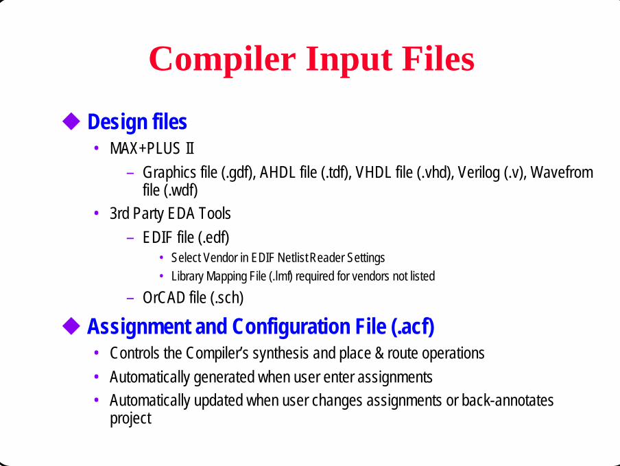
Compiler Input Files
u Design files• MAX+PLUS II
– Graphics file (.gdf), AHDL file (.tdf), VHDL file (.vhd), Verilog (.v), Wavefromfile (.wdf)
• 3rd Party EDA Tools– EDIF file (.edf)
• Select Vendor in EDIF Netlist Reader Settings• Library Mapping File (.lmf) required for vendors not listed
– OrCAD file (.sch)
u Assignment and Configuration File (.acf)• Controls the Compiler’s synthesis and place & route operations• Automatically generated when user enter assignments• Automatically updated when user changes assignments or back-annotates
project

© CIC Altera Max+PlusII Y.T.Chou/Steven Page 137
Compiler Output Files
u Design verification files• MAX+PLUS II
– Simulation Netlist File (.snf)• 3rd Party EDA Tools
– VHDL netlist file (.vho)– EDIF netlist file (.edo)– Verilog netlist file (.vo)– Standard Delay Format SDF file (.sdo)
u Programming files• Programmer Object file (.pof)• SRAM Object file (.sof)• JEDEC file (.jed)
© CIC Altera Max+PlusII Y.T.Chou/Steven Page 138
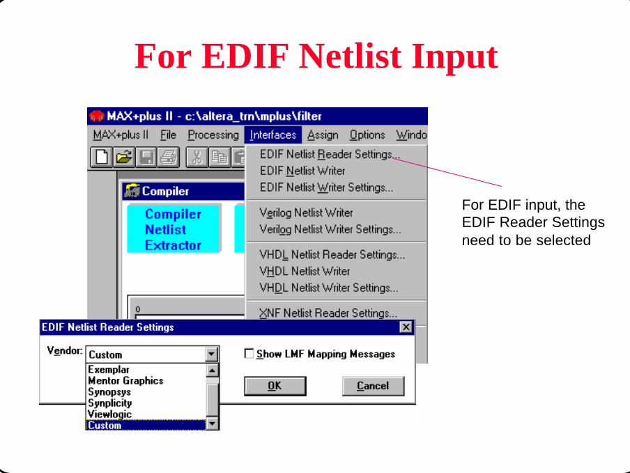
For EDIF Netlist Input
For EDIF input, theEDIF Reader Settingsneed to be selected

© CIC Altera Max+PlusII Y.T.Chou/Steven Page 139
VHDL Netlist Reader Settings
Select VHDL versionand Library names

© CIC Altera Max+PlusII Y.T.Chou/Steven Page 140
For EDIF Netlist Output
Need to select vendor inEDIF Netlist Writer settings
For EDIF output, theEDIF Netlist Writer needsto be selected.

© CIC Altera Max+PlusII Y.T.Chou/Steven Page 141
Verilog Netlist Writer & Writer Settings
Select Verilog NetlistWriter Settingsto adjust Verilog outputs
Select Verilog NetlistWriter to output Verilogfile for Verilog simulator

© CIC Altera Max+PlusII Y.T.Chou/Steven Page 142
VHDL Netlist Writer & Writer Settings
Select VHDL NetlistWriter Settingsto adjust the VHDL output
Select VHDL NetlistWriter to output VHDL file for VHDL simulator
© CIC Altera Max+PlusII Y.T.Chou/Steven Page 143
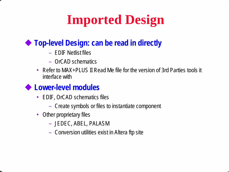
Imported Design
u Top-level Design: can be read in directly– EDIF Netlist files– OrCAD schematics
• Refer to MAX+PLUS II Read Me file for the version of 3rd Parties tools it interface with
u Lower-level modules• EDIF, OrCAD schematics files
– Create symbols or files to instantiate component • Other proprietary files
– JEDEC, ABEL, PALASM– Conversion utilities exist in Altera ftp site

© CIC Altera Max+PlusII Y.T.Chou/Steven Page 144
Compiler Modules - (1)
u Compiler Netlist Extractor• The Compiler module that converts each design file in a project (or each cell of an
EDIF input file) into a separate binary CNF (Compiler Netlist File)• The Compiler Netlist Extractor also creates a single HIF that documents the
hierarchical connections between design files• This module contains a built-in EDIF Netlist Reader, VHDL Netlist Reader, and XNF
Netlist Reader for use with MAX+PLUS II. • During netlist extraction, this module checks each design file for problems such as
duplicate node names, missing inputs and outputs, and outputs that are tied together.
• If the project has been compiled before, the Compiler Netlist Extractor creates new CNFs and a HIF only for those files that have changed since the last compilation, unless Total Recompile (File menu) is turned on

© CIC Altera Max+PlusII Y.T.Chou/Steven Page 145
Compiler Modules - (2)
u Database Builder• The Compiler module that builds a single, fully flattened project database that
integrates all the design files in a project hierarchy• As it creates the database, the Database Builder examines the logical completeness
and consistency of the project, and checks for boundary connectivity and syntactical errors (e.g., a node without a source or destination)

© CIC Altera Max+PlusII Y.T.Chou/Steven Page 146
Compiler Modules - (3)
u Logic Synthesizer• The Compiler module that synthesizes the logic in a project's design files. • The Logic Synthesizer calculates Boolean equations for each input to a primitive
and minimizes the logic according to your specifications• The Logic Synthesizer also synthesizes equations for flip-flops to implement state
registers of state machines• As part of the logic minimization and optimization process, logic and nodes in the
project may be changed or removed• Throughout logic synthesis, the Logic Synthesizer detects and reports errors such
as illegal combinatorial feedback and tri-state buffer outputs wired together ("wired ORs")
u Design Doctor Utility• The Compiler utility that checks each design file in a project for poor design
practices that may cause reliability problems when the project is implemented in one or more devices
© CIC Altera Max+PlusII Y.T.Chou/Steven Page 147
Compiler Modules - (4)
u Partitioner• The Compiler module that partitions the logic in a project among multiple devices
from the same device family• Partitioning occurs if you have created two or more chips in the project's design files
or if the project cannot fit into a single device• This module splits the database updated by the Logic Synthesizer into different
parts that correspond to each device• A project is partitioned along logic cell boundaries, with a minimum number of pins
used for inter-device communication

© CIC Altera Max+PlusII Y.T.Chou/Steven Page 148
Compiler Modules - (5)
u Fitter• The Compiler module that fits the logic of a project into one or more devices• Using the database updated by the Partitioner, the Fitter matches the logic
requirements of the project with the available resources of one or more devices• It assigns each logic function to the best logic cell location and selects appropriate
interconnection paths and pin assignments• The Fitter module generates a “fit file”(*.fit) that documents pin, buried logic cell,
chip, clique, and device assignments made by the Fitter module in the last successful compilation
• Regardless of whether a fit is achieved, the Fitter generates a report file(*.rpt) that shows how the project is implemented in one or more devices

© CIC Altera Max+PlusII Y.T.Chou/Steven Page 149
Compiler Modules - (6)
u SNF(Simulation Netlist File) Extractor• Functional SNF Extractor
– The Compiler module that creates a functional SNF containing the logic information required for functional simulation.
– Since the functional SNF is created before logic synthesis, partitioning, and fitting are performed, it includes all nodes in the original design files for the project
• Timing SNF Extractor– The Compiler module that creates a timing SNF containing the logic and timing
information required for timing simulation, delay prediction, and timing analysis– The timing SNF describes a project as a whole. Neither timing simulation nor
functional testing is available for individual devices in a multi-device project.• Linked SNF Extractor
– The Compiler module that creates a linked SNF containing timing and/or functional information for several projects
– A linked SNF of a super-project combines the timing and/or functional information for each project, allowing you to perform a board-level simulation
© CIC Altera Max+PlusII Y.T.Chou/Steven Page 150
Compiler Modules - (7)
u Netlist Writer• EDIF Netlist Writer
– The Compiler module that creates one or more EDIF output files(*.edo). It can also generate one or more optional SDF output files(*.sdo).
– EDIF output Files contain the logic and timing information for the optimized project and can be used with industry-standard simulators. An EDIF Output File is generated for each device in a project.
• Verilog Netlist Writer– The Compiler module that creates one or more Verilog output files(*.vo). It can
also generate one or more optional SDF output files.• VHDL Netlist Writer
– The Compiler module that creates one or more VHDL output files(*.vho). It can also generate one or more optional VITAL-compliant SDF output files.

© CIC Altera Max+PlusII Y.T.Chou/Steven Page 151
Compiler Modules - (8)
u Assembler• The Compiler module that creates one or more programming files for programming
or configuring the device(s) for a project• The assembler generates one or more device programming files
– POFs and JEDEC Files are always generated– SOFs, Hex Files, and TTFs are also generated if the project uses FLEX
devices– You can generate additional device programming files for use in other
programming environment. For example, you can create SBF and RBF to configure FLEX devices.
– File format:• POF: Programming Object File• SOF: SRAM Object File• TTF: Tabular Text File• HEX: Intel-format Hexadecimal File• SBF: Serial Bitstream File• RBF: Raw Binary File
© CIC Altera Max+PlusII Y.T.Chou/Steven Page 152
u Select functional compilation or timing compilationu Assignmentsu Run the compilationu Consult the report file (.rpt) or the Floorplan Editor for
device utilization summaries and synthesis and place & route results
Compiling a Project
© CIC Altera Max+PlusII Y.T.Chou/Steven Page 153
The Functional Compilation Process
n Compiler Netlist Extractor builds the .cnf netlist file and checks for syntax errors
n Database Builder constructs the node name database n Functional SNF Extractor build .snf file for functional
simulation
© CIC Altera Max+PlusII Y.T.Chou/Steven Page 154
The Timing Compilation Processn Compiler Netlist Extractor and Database Builder build netlist
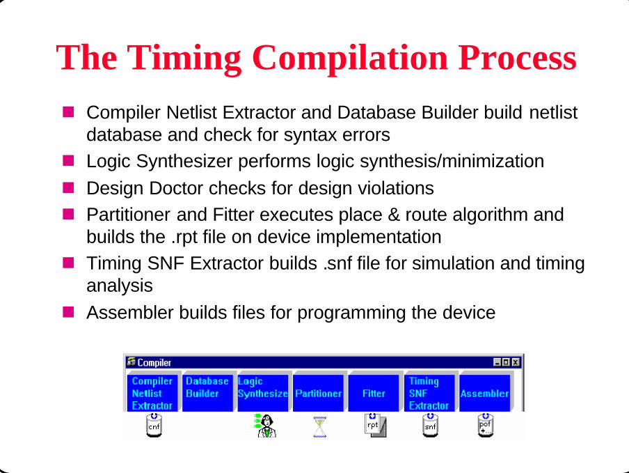
database and check for syntax errorsn Logic Synthesizer performs logic synthesis/minimizationn Design Doctor checks for design violationsn Partitioner and Fitter executes place & route algorithm and
builds the .rpt file on device implementationn Timing SNF Extractor builds .snf file for simulation and timing
analysisn Assembler builds files for programming the device

© CIC Altera Max+PlusII Y.T.Chou/Steven Page 155
Compiler Processing Options
u Functional• Compilation generates file for Functional Simulation
– Functional SNF file (.snf)
u Timing• Compilation generates user selectable files for
– Timing Simulation and Timing Analysis• Timing SNF file (.snf)
– 3rd party EDA Simulation• Verilog file (.vo)• VHDL file (.vho)• SDF file (.sdo)
– Device Programming• Altera Programmer file (e.g. .pof, .sof)

© CIC Altera Max+PlusII Y.T.Chou/Steven Page 156
Compilation Process Settings - (6)
u Customize the report file settings
Menu: Processing -> Report File Settings...
© CIC Altera Max+PlusII Y.T.Chou/Steven Page 157
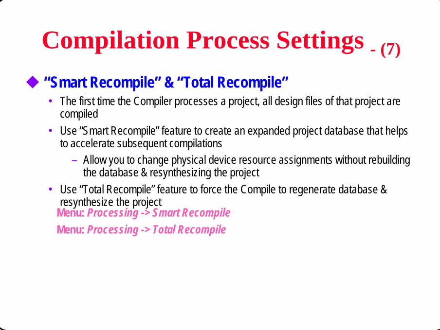
Compilation Process Settings - (7)
u “Smart Recompile” & “Total Recompile”• The first time the Compiler processes a project, all design files of that project are
compiled• Use “Smart Recompile”feature to create an expanded project database that helps
to accelerate subsequent compilations– Allow you to change physical device resource assignments without rebuilding
the database & resynthesizing the project• Use “Total Recompile”feature to force the Compile to regenerate database &
resynthesize the project Menu: Processing -> Smart RecompileMenu: Processing -> Total Recompile

© CIC Altera Max+PlusII Y.T.Chou/Steven Page 158
Assign Menu
• You can specifies optional sections to be included in the report file(*.rpt), which is created by the Fitter when a project is compiled
– All sections are included by default

© CIC Altera Max+PlusII Y.T.Chou/Steven Page 159
Assignments Control
u Device FIT• MAX+PLUS II default settings are designed for maximum fitfit-ability• Almost all assignments affect fitting
u Device Utilization• Circuit design• Logic assignment
u Performance• Circuit design• Logic assignments• Logic placements
© CIC Altera Max+PlusII Y.T.Chou/Steven Page 160
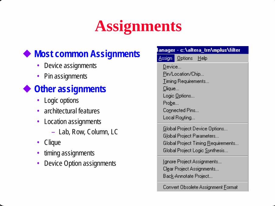
Assignments
u Most common Assignments• Device assignments• Pin assignments
u Other assignments• Logic options• architectural features• Location assignments
– Lab, Row, Column, LC• Clique• timing assignments• Device Option assignments

© CIC Altera Max+PlusII Y.T.Chou/Steven Page 161
Making Device Assignment
u Select Device• Specific device• Auto
– MAX+PLUS II chooses smallest and fastest device the design fits into
Selectdevice Family
Autodevice selection
Specificdevice selection
© CIC Altera Max+PlusII Y.T.Chou/Steven Page 162
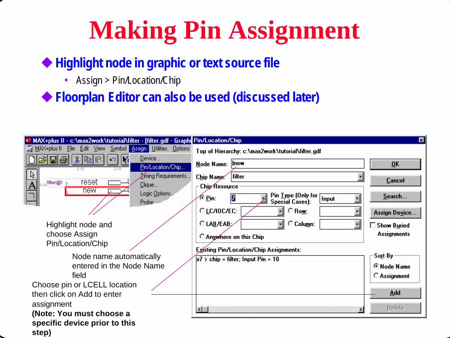
Making Pin AssignmentuHighlight node in graphic or text source file
• Assign > Pin/Location/Chip
uFloorplan Editor can also be used (discussed later)
Highlight node and choose Assign Pin/Location/Chip
Node name automatically entered in the Node Name field
Choose pin or LCELL location then click on Add to enter assignment(Note: You must choose a specific device prior to this step)

© CIC Altera Max+PlusII Y.T.Chou/Steven Page 163
Logic Synthesis Style
u The most common way toward adjusting these assignments is to apply the predefined Logic Synthesis Style toward the different portion of your design:
• Normal• Fast• WYSIWYG
u Each of the Logic Synthesis Styles is a collection of both logic synthesis options and individual architectural settings

© CIC Altera Max+PlusII Y.T.Chou/Steven Page 164
Global Project Logic Synthesis Styleu Choose Assign then Global Project Logic Synthesisu Select from predefined synthesis style
• NORMAL (default), FAST or WYSIWYG
u Or create user tailored settings

© CIC Altera Max+PlusII Y.T.Chou/Steven Page 165
Assign Logic Synthesis Style Locally
Select Logic Synthesis Style

© CIC Altera Max+PlusII Y.T.Chou/Steven Page 166
Individual Logic Option Assignmentu Provides controls to turn individual architectural features
and synthesis algorithms on or offGray or Default (default): set by higher level or global settingCheck or Auto: enable featureBlank or Ignore: disable feature

© CIC Altera Max+PlusII Y.T.Chou/Steven Page 167
Location assignments
Select Pin/Location/Chip ...
Select Location

© CIC Altera Max+PlusII Y.T.Chou/Steven Page 168
Clique Assignments
Select Clique
Enter clique name
Click Add to addassignment, click OK to close window
Clique assignments tell the compiler toplace the nodes with the same clique assignmentclose together inside the device.

© CIC Altera Max+PlusII Y.T.Chou/Steven Page 169
Timing Requirements Assignments
FLEX devices onlyu Specifies desired speed performanceu Use after performing timing analysis to improve specific
timing pathu Localized control
• Highlight node, pin or logic block• Choose Assign then Timing Requirements• Assign desired tpd, tco, tsu, fmax values
u Global control• Choose Assign then Global Project Timing Requirements• Assign desired tpd, tco, tsu, fmax values
© CIC Altera Max+PlusII Y.T.Chou/Steven Page 170
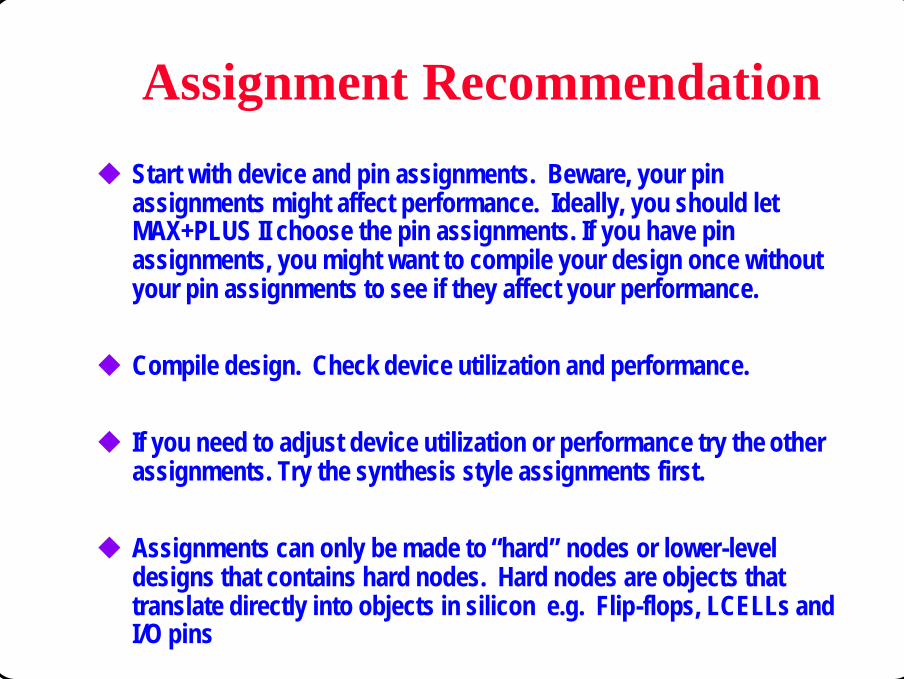
Assignment Recommendation
u Start with device and pin assignments. Beware, your pin assignments might affect performance. Ideally, you should let MAX+PLUS II choose the pin assignments. If you have pin assignments, you might want to compile your design once without your pin assignments to see if they affect your performance.
u Compile design. Check device utilization and performance.
u If you need to adjust device utilization or performance try the other assignments. Try the synthesis style assignments first.
u Assignments can only be made to “hard” nodes or lower-level designs that contains hard nodes. Hard nodes are objects that translate directly into objects in silicon e.g. Flip-flops, LCELLs and I/O pins

© CIC Altera Max+PlusII Y.T.Chou/Steven Page 171
Ignore or Clear Assignments
Ignore ProjectAssignments
Clear ProjectAssignments

© CIC Altera Max+PlusII Y.T.Chou/Steven Page 172
Global Project Device Options Window contains options related to the operation of the device rather than options that affect the logic synthesis and place & route of the design. For example,FLEX Device
• configuration scheme• multi-volt I/O
MAX Device• Enable JTAG support• security bit
Global Project Device Options

© CIC Altera Max+PlusII Y.T.Chou/Steven Page 173
More Compiler Processing Options
u Design Doctor• Checks for common design errors
u Fitter Settings• Set place & route options
u Smart Recompile• Faster compilation time
u Total Recompile• Recompile every file

© CIC Altera Max+PlusII Y.T.Chou/Steven Page 174
Compile the Design
n Start Button starts compilation processn Messages are displayed by the Message Processor
– Info– Warning– Error
Start Compilation
Messages

© CIC Altera Max+PlusII Y.T.Chou/Steven Page 175
The Report File
n Project summary– Device assignments– Error summary– Device pin-out diagram (useful for PCB layout)
n Resource utilization– Pin– LCELL– Equations
n Compiler resources– Compilation time– Memory usage Open report file by
double clicking on the rapt icon

© CIC Altera Max+PlusII Y.T.Chou/Steven Page 176
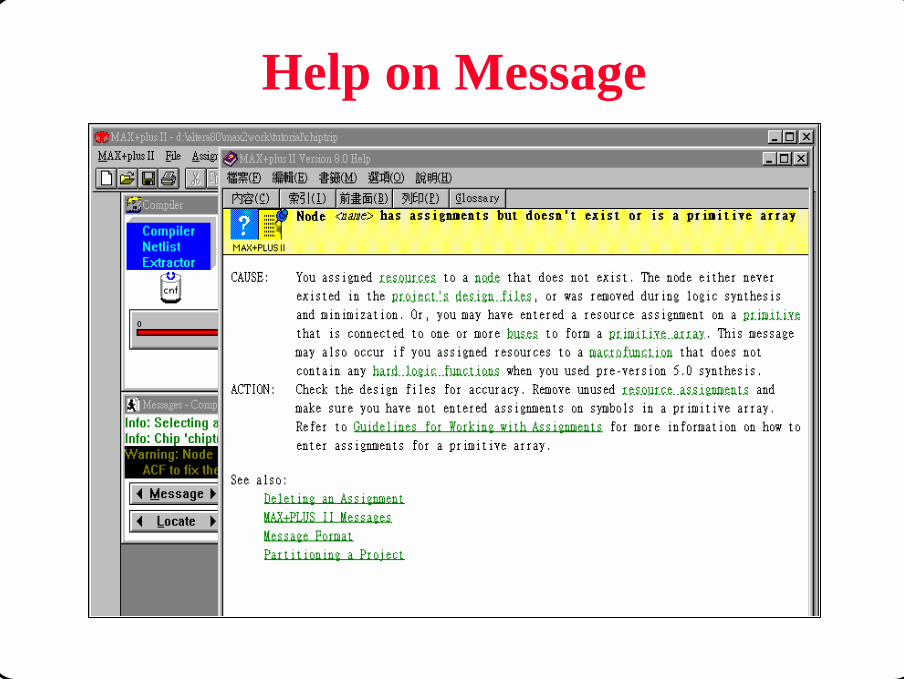
Checking the Messages
u Check the messages in Message Processor• In Message Processor window, choose the message and click the HELP on Message to understand the meaning of the message, its cause and the possible solutions (suggested actions)
u Error location• In Message Processor window, choose the message and click the Locate button
to locate the source of the message in the original design files• You can turn on Locate in Floorplan Editor and click Local All
button to find the corresponding nodes in the Floorplan Editor
© CIC Altera Max+PlusII Y.T.Chou/Steven Page 177
Help on Message

© CIC Altera Max+PlusII Y.T.Chou/Steven Page 178
Checking the Reports
u Check the report file• Use Text Editor or double click the Report File icon• Device summary, project compilation messages, file hierarchy, resource usage,
routing resources, logic cell interconnections, ...

© CIC Altera Max+PlusII Y.T.Chou/Steven Page 179
Viewing Report File
© CIC Altera Max+PlusII Y.T.Chou/Steven Page 180
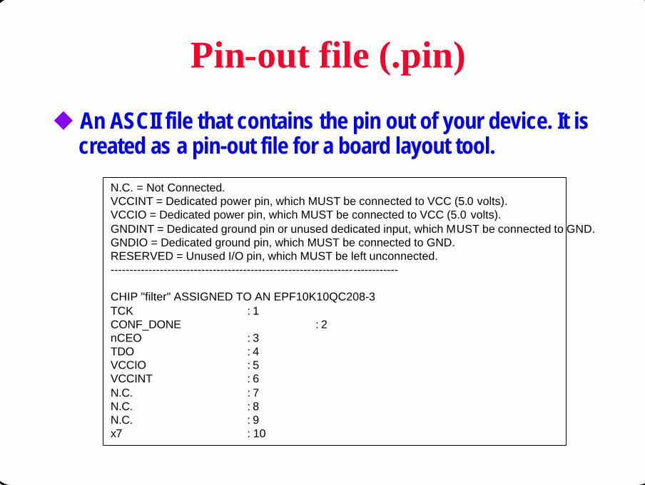
Pin-out file (.pin)
u An ASCII file that contains the pin out of your device. It is created as a pin-out file for a board layout tool.
N.C. = Not Connected.VCCINT = Dedicated power pin, which MUST be connected to VCC (5.0 volts).VCCIO = Dedicated power pin, which MUST be connected to VCC (5.0 volts).GNDINT = Dedicated ground pin or unused dedicated input, which MUST be connected to GND.GNDIO = Dedicated ground pin, which MUST be connected to GND.RESERVED = Unused I/O pin, which MUST be left unconnected.----------------------------------------------------------------------------
CHIP "filter" ASSIGNED TO AN EPF10K10QC208-3TCK : 1CONF_DONE : 2nCEO : 3TDO : 4VCCIO : 5VCCINT : 6N.C. : 7N.C. : 8N.C. : 9x7 : 10
© CIC Altera Max+PlusII Y.T.Chou/Steven Page 181
Floorplan Editor
u Graphical user interface for viewing/creating resource assignments
• Pins• Logic cells• Cliques• Logic options
u Drag-and-drop capability for assigning pins/logic cellsu Graphical view of current assignments as well as last
compilation resultsu LAB view or external chip view
© CIC Altera Max+PlusII Y.T.Chou/Steven Page 182
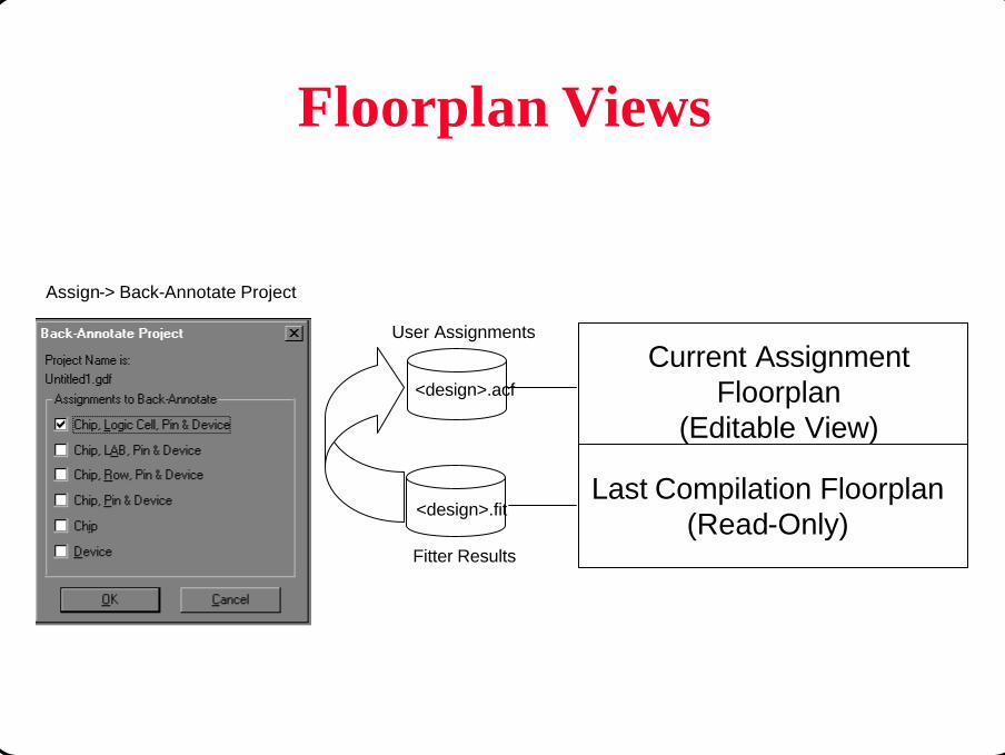
Floorplan Views
Current Assignment Floorplan
(Editable View)
Last Compilation Floorplan(Read-Only)
<design>.fit
<design>.acf
Assign-> Back-Annotate Project
User Assignments
Fitter Results

© CIC Altera Max+PlusII Y.T.Chou/Steven Page 183
Floorplan Editor (Read Only)
u Last Compilation Floorplan Full Screen LAB View with Report File Equation Viewer
Fan-in and Fan-out
Highlighted LCELL
LCELL equation
Display control

© CIC Altera Max+PlusII Y.T.Chou/Steven Page 184
Floorplan Editor (Read Only)
u Last Compilation Floorplan Device View
Pin number
Pin name
Color Legenddefinition

© CIC Altera Max+PlusII Y.T.Chou/Steven Page 185
Floorplan Editor (Editable)
u Current Assignment view has drag and drop capability (Note: Auto Device can not be used)
Click on Node ,hold left mouse, drag to location

© CIC Altera Max+PlusII Y.T.Chou/Steven Page 186
Floorplan Editor (Editable)

© CIC Altera Max+PlusII Y.T.Chou/Steven Page 187
Project Compilation Recommendations
u Use assignments after design analysis to improve fitting or performance
u Use the Report File to find specific information on the design
u Use the Floorplan Editor to see results of Assignments

© CIC Altera Max+PlusII Y.T.Chou/Steven Page 188
Report File Equation Viewer

© CIC Altera Max+PlusII Y.T.Chou/Steven Page 189
Routing Statistics

© CIC Altera Max+PlusII Y.T.Chou/Steven Page 190
Floorplan Editor Utilities Menu
u To find text, node, ...• “Find Text”command: to search the current chip for
the first occurrence of the specified text• “Find Node”command: to find one or more nodes or
other logic function(s) in the design file or in the floorplan
u To help running timing analysis• You can specify source and destination nodes in the
floorplan to run timing analysis
Floorplan Editor Utilities Menu
© CIC Altera Max+PlusII Y.T.Chou/Steven Page 191
Assigning Logic to Physical Resources
u Use Floorplan Editor to assign logic to physical resources• You can assign logic to a device, to any row or column within a device, or to a
specific LAB, pin, logic cell, or I/O cell in Floorplan Editor very easily• To toggle between current assignment & last compilation floorplan
Menu: Layout -> Current Assignments FloorplanMenu: Layout -> Last Compilation Floorplan
u Back-annotate the floorplan for subsequent compilation• If necessary, you can back-annotate the floorplan to ACF(Assignment &
Configuration File) and it is useful for retaining the current resource and device assignments for future compilationsMenu: Assign -> Back-Annotate Project...

© CIC Altera Max+PlusII Y.T.Chou/Steven Page 192
Current Pin Assignment Floorplan

© CIC Altera Max+PlusII Y.T.Chou/Steven Page 193
Current LAB Assignment Floorplan
Anywhereon Device
Anywhereon thisColumn
Anywhereon thisRow

© CIC Altera Max+PlusII Y.T.Chou/Steven Page 194
DesignFiles
Simulation/Timing Files
Project Compilation Summary
.gdf
.tdf
.vhd
.sch
.edf
.snf
MAX+PLUS II CompilerCompiler Netlist
Extractor (includesall netlist readers
Functional, Timing,or Linked SNF
Extractor
EDIF, VHDL &Verilog Netlist
Writers
DatabaseBuilder
Partitioner
DesignDoctor
LogicSynthesizer
Fitter
Assembler
.edo .vo .vho 3rd PartyEDA Files
ProgrammingFiles
.pof
ReportFiles
.rpt
.sdo
.wdf
.v

© CIC Altera Max+PlusII Y.T.Chou/Steven Page 195
Project Verificationu Project Verification Methodologyu MAX+PLUS II Simulatoru Functional Simulationu Timing Simulationu Timing Analysis
© CIC Altera Max+PlusII Y.T.Chou/Steven Page 196
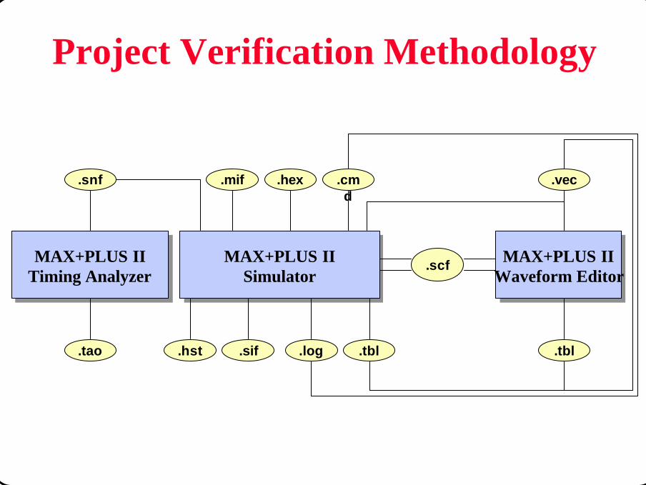
Project Verification Methodology
.hst .sif .tbl.log
.snf
.tao
MAX+PLUS IITiming Analyzer
MAX+PLUS IISimulator
MAX+PLUS IIWaveform Editor
.scf
.tbl
.cmd
.vec.hex.mif

© CIC Altera Max+PlusII Y.T.Chou/Steven Page 197
System Production
Design Specification
Design Entry
Project Compilation
Device Programming
In-System Verification
Design Modification
SimulationTiming Analysis
Command-LineMode

© CIC Altera Max+PlusII Y.T.Chou/Steven Page 198
MAX+PLUS II Simulator
MAX+PLUS IIWaveform Editor
.scf
.snf
MAX+PLUS IIText Editor
MAX+PLUS IISimulator
MAX+PLUS IICompiler
.scf
.vec
MAX+PLUS IIWaveform Editor

© CIC Altera Max+PlusII Y.T.Chou/Steven Page 199
MAX+PLUS II Simulation
u Create Simulation Stimulus• Waveform• Vector
u Run Functional Simulation• Fast compilation• Logical model only, no logic synthesis• All nodes are retained and can be simulated• Outputs are updated without delay
u Run Timing Simulation• Slower compilation• Timing model: logical & delay model• Nodes may be synthesized away• Outputs are updated after delay

© CIC Altera Max+PlusII Y.T.Chou/Steven Page 200
Simulation Waveform
u Stimulus Waveform• Waveform Editor File (.scf)• Control
– Clock: Use built-in clock generator– Others: Hand drawn with overwrite/copy/paste/repeat
• Data– Counting patterns: Use built-in binary or gray code generator– Others: Enter with overwrite/copy/paste/repeat
u Reference Compare waveform• Waveform Editor File (.scf)• Draw or save previous simulation result as reference waveform• Use with Compare after new simulation run to verify output

© CIC Altera Max+PlusII Y.T.Chou/Steven Page 201
Create Waveform Simulation Stimulus
n Open Waveform Editorn Select Enter Nodes from SNF… from Node menun Enter Nodes into Selected Nodes & Groups field
Select Node
Enter Node into Selected Nodes & Groups field
© CIC Altera Max+PlusII Y.T.Chou/Steven Page 202
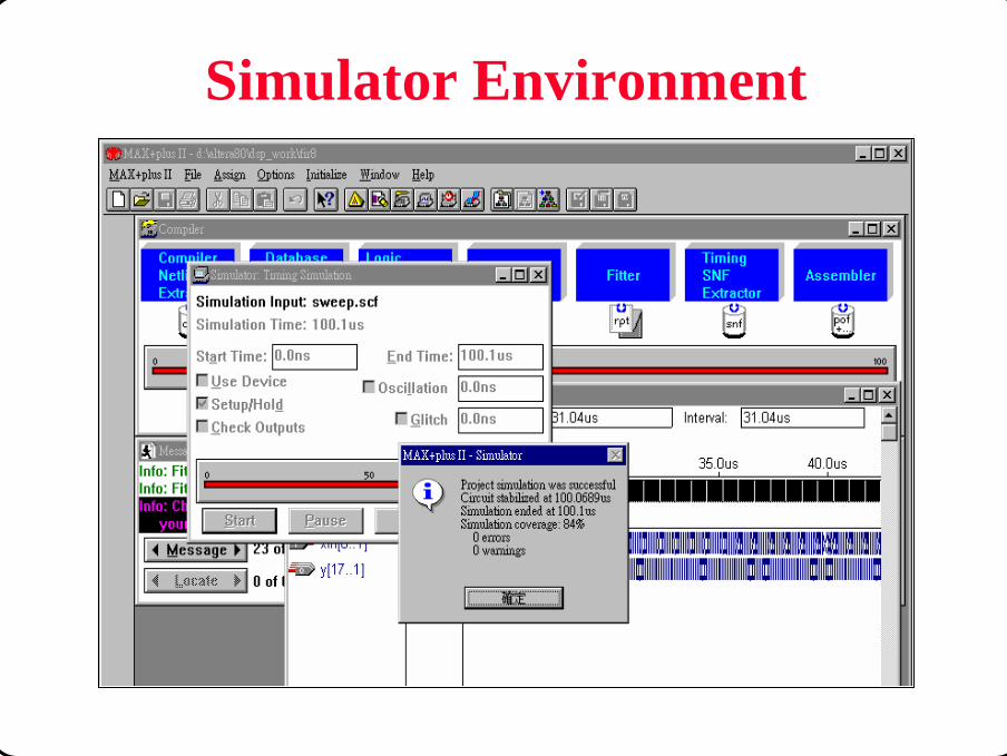
Simulator Environment

© CIC Altera Max+PlusII Y.T.Chou/Steven Page 203
Grid Control
u Snap to Grid• On: waveforms drawn increments of grid size• Off: waveforms can be drawn to any size
Set Grid size
© CIC Altera Max+PlusII Y.T.Chou/Steven Page 204
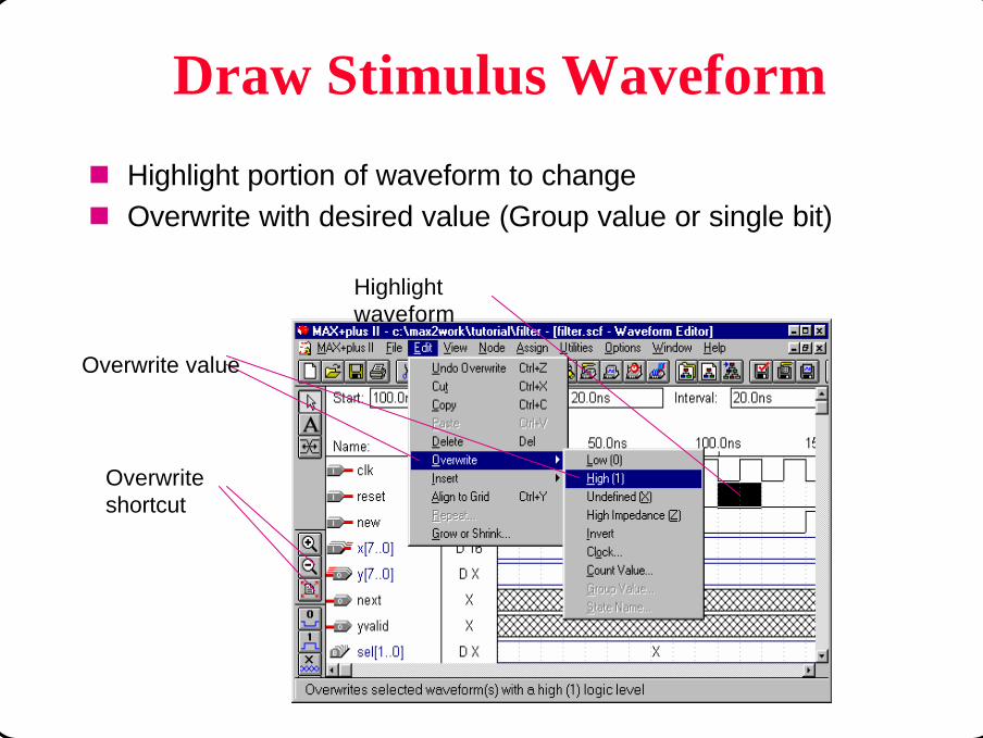
Draw Stimulus Waveform
n Highlight portion of waveform to changen Overwrite with desired value (Group value or single bit)
Highlight waveform
Overwrite value
Overwrite shortcut
© CIC Altera Max+PlusII Y.T.Chou/Steven Page 205
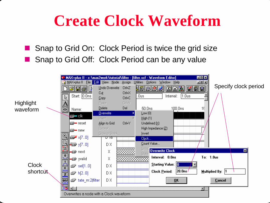
Create Clock Waveform
n Snap to Grid On: Clock Period is twice the grid sizen Snap to Grid Off: Clock Period can be any value
Highlight waveform
Clock shortcut
Specify clock period

© CIC Altera Max+PlusII Y.T.Chou/Steven Page 206
Create Counting Pattern
n Make sure your counting frequency matches your clock frequency
Highlight waveform
Pattern shortcut
Specify counting pattern
Specify counting frequency

© CIC Altera Max+PlusII Y.T.Chou/Steven Page 207
Grouping Signals and Set Radix
n Highlight waveforms to be grouped– MSB must be the top waveform
n Enter Group Name and set Radix Enter Group Name
Set radix

© CIC Altera Max+PlusII Y.T.Chou/Steven Page 208
Save the Waveform Stimulus File
n Save the waveform stimulus file with .scf extensionn MAX+PLUS II will use Project name as default file name
Waveform File Name
Project Directory

© CIC Altera Max+PlusII Y.T.Chou/Steven Page 209
Create Vector Simulation Stimulusn Open Text Editorn Type in vector stimulus
– Clock
– Pattern
– Output
% units default to ns %START 0 ;STOP 1000 ;INTERVAL 100 ;INPUTS CLOCK ;PATTERN0 1 ; % CLOCK ticks every 100 ns %
INPUTS A B ;PATTERN0> 0 0220> 1 0320> 1 1 570> 0 1720> 1 1;
OUTPUTS Y1 Y0 ;PATTERN % check output at every Clock pulse %= X X= 0 0 = 0 1= 1 0= 1 1;

© CIC Altera Max+PlusII Y.T.Chou/Steven Page 210
Save the Vector Stimulus File
n Save the vector stimulus file with .vec extension– You must change the .vec extension since MAX+PLUS
II defaults to .tdf extension for text files
Change the extension to .vec

© CIC Altera Max+PlusII Y.T.Chou/Steven Page 211
Select Simulation Stimulus File
n Defaults to .scf filen For vector input stimulus, set Vector Files Input to .vec file
Set to .vec file

© CIC Altera Max+PlusII Y.T.Chou/Steven Page 212
Specify Length of Simulation
u Specify maximum length of simulation time with End Time

© CIC Altera Max+PlusII Y.T.Chou/Steven Page 213
Run Functional Simulationn Click on Start then Open SCF to see result
Output change on clock edge
Open .scf file
Click on Start Button
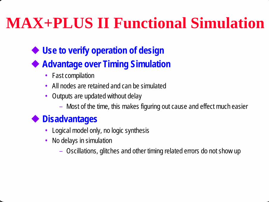
© CIC Altera Max+PlusII Y.T.Chou/Steven Page 214
MAX+PLUS II Functional Simulation
u Use to verify operation of designu Advantage over Timing Simulation
• Fast compilation• All nodes are retained and can be simulated• Outputs are updated without delay
– Most of the time, this makes figuring out cause and effect much easier
u Disadvantages• Logical model only, no logic synthesis• No delays in simulation
– Oscillations, glitches and other timing related errors do not show up

© CIC Altera Max+PlusII Y.T.Chou/Steven Page 215
Run Timing Simulation
n Click on Start then Open SCF to see result
Output change after timing delay
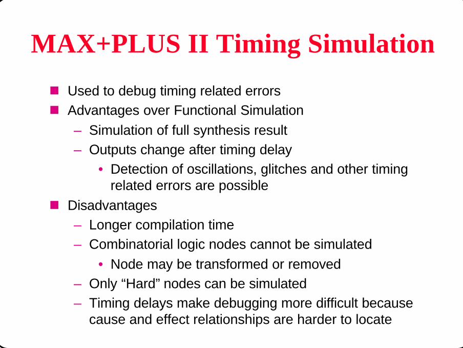
© CIC Altera Max+PlusII Y.T.Chou/Steven Page 216
MAX+PLUS II Timing Simulation
n Used to debug timing related errorsn Advantages over Functional Simulation
– Simulation of full synthesis result– Outputs change after timing delay
• Detection of oscillations, glitches and other timing related errors are possible
n Disadvantages– Longer compilation time– Combinatorial logic nodes cannot be simulated
• Node may be transformed or removed– Only “Hard”nodes can be simulated– Timing delays make debugging more difficult because
cause and effect relationships are harder to locate

© CIC Altera Max+PlusII Y.T.Chou/Steven Page 217
uOpen first channel fileuChoose Compare under File menuuSelect the name of the second channel file with the
Compare dialog boxuWaveforms from the first channel file are drawn in black.
Waveforms from the second channel file are drawn in red on top of the black waveforms. Deviations of second channel file can easier be spotted.
Compare Two Simulation Files
Comparing Different Simulations

© CIC Altera Max+PlusII Y.T.Chou/Steven Page 218
Project Simulation Recommendations
u Use built-in clock generator to create clocku Use built-in count generator to create test patternu Use Functional Simulation to verify proper operationu Use Timing Simulation to examine signal delay effectsu Use Compare function to verify outputu Use the dynamic link ( Find Node in Design File ) to go to
source file to make any necessary corrections
© CIC Altera Max+PlusII Y.T.Chou/Steven Page 219
Simulation Input & Output Files
u Specify simulation input and output files
• You can specify SCF or VEC file as the source of simulation input vectorsMenu: File -> Inputs/Outputs...
– VEC file will be converted into SCF file by Simulator
– You can specify a history(*.hst) or log(*.log) file to record simulation commands and outputs
• During and after simulation, the simulation results are written to the SCF file, you can create another ASCII-format table fileMenu: File -> Create Table File...
– TBL file format is a subset of VEC file format
– A TBL file can be specified as a vector input file for another simulation
File Menu

© CIC Altera Max+PlusII Y.T.Chou/Steven Page 220
Memory Initialization
u Give memory initialization values for functional simulation• To generate memory initialization values in Simulator
Menu: Initialize -> Initialize Memory...• You can save the data in the Initialize Memory dialog box to a Hexadecimal File
(*.hex) or Memory Initialization File (*.mif) for future useMenu: Initialize -> Initialize Memory... -> Export File...
– An MIF is used as an input file for memory initialization in the Compiler and Simulator. You can also use a Hexadecimal File (.hex) to provide memory initialization data.
• You can load the memory initialization data for a memory block that is saved in a HEX or MIF fileMenu: Initialize -> Initialize Memory... -> Import File...
Initialize Menu

© CIC Altera Max+PlusII Y.T.Chou/Steven Page 221
Initialize Memory Window
© CIC Altera Max+PlusII Y.T.Chou/Steven Page 222
Memory Initialization File FormatsWIDTH = 16;DEPTH = 256;
ADDRESS_RADIX = HEX;DATA_RADIX = HEX;
CONTENT BEGIN0 : 0000;1 : 0000;2 : 0000;3 : 0000;4 : 0000;5 : 0000;6 : 0000;7 : 0000;8 : ffff;9 : ffff;a : ffff;b : ffff;c : ffff;d : ffff;e : ffff;f : ffff;
...ff : 0000;
END;
:020000000000fe:020001000000fd:020002000000fc:020003000000fb:020004000000fa:020005000000f9:020006000000f8:020007000000f7:02000800fffff8:02000900fffff7:02000a00fffff6:02000b00fffff5:02000c00fffff4:02000d00fffff3:02000e00fffff2:02000f00fffff1...:0200ff000000ff:00000001ff
MIF file example
HEX file example

© CIC Altera Max+PlusII Y.T.Chou/Steven Page 223
MIF File Format
u To edit a MIF file...• MIF file is an ASCII text file that specifies the initial content of a memory block
– You can create an MIF in the MAX+PLUS II Text Editor or any ASCII text editor
– You can also very easily generate an MIF by exporting data from the Simulator's Initialize Memory dialog box
• Example:
DEPTH = 32; % Memory depth and width are required %WIDTH = 14; % Enter a decimal number %ADDRESS_RADIX = HEX; % Address and value radixes are optional %DATA_RADIX = HEX; % Enter BIN, DEC, ,OCT or HEX(default) %
-- Specify values for addresses, which can be single address or rangeCONTENTBEGIN[0..F] : 3FFF; % Range--Every address from 0 to F = 3FFF %6 : F; % Single address--Address 6 = F %8 : F E 5; % Range starting from specific address %
END; % Addr[8]=F, Addr[9]=E, Addr[A]=5 %

© CIC Altera Max+PlusII Y.T.Chou/Steven Page 224
Notes for Compiling &Simulating RAM / ROM - (1)
u Remember: MAX+PLUS II Compiler uses MIF or HEX file(s) tocreate ROM or RAM initialization circuit in FLEX 10K EAB
• Specify the LPM_FILE parameter to a MIF or HEX file for each RAM and ROM block
– Memory initialization file is optional for RAM– Using MIF files is recommended because its file format is simple
u If the memory initial file does not exist when MAX+PLUS II Compiler is generating functional SNF file, you must initialize the memory by using Initialize Memory command before starting the functional simulation
• MAX+PLUS II Compiler reports an warning when it can’t read the memory initialization file when processing Functional SNF Extractor
• However, the memory initialization file must exist when MAX+PLUS II processes Timing SNF Extractor

© CIC Altera Max+PlusII Y.T.Chou/Steven Page 225
Notes for Compiling &Simulating RAM / ROM - (2)
u If you do not have MIF or HEX files, do the following:• Run MAX+PLUS II Compiler to generate a functional SNF file first• Then invoke MAX+PLUS II Simulator, use Memory Initialization command to create
memory content for each ROM or RAM block• Export memory content to a MIF or HEX file
– And now, you can perform functional simulation for your project• Invoke MAX+PLUS II Compiler again, turn on “Timing SNF Extractor”and start
complete compilation for FLEX 10K devices

© CIC Altera Max+PlusII Y.T.Chou/Steven Page 226
Node/Group Initialization
u Specify initial logic levels for nodes/ groups
• You can change the initial logic levels of registered nodes/groups in the SNF file for the project before you begin simulationMenu: Initialize -> Initialize Nodes/Groups...
– You can also specify an initial state name for a group that represents a state machine.
• By default, all register outputs are initialized to 0 and pin inputs are initialized to the first logic level provided in the current SCF
© CIC Altera Max+PlusII Y.T.Chou/Steven Page 227
Saving Initialization Values
u Save the initialization values to SIF file• You can save current initialized node and group
logic levels and memory values to a Simulation Initialization File(*.sif)Menu: Initialize -> Save Initialization As...
• To retrieve initialized node, group, and memory values stored in a SIF fileMenu: Initialize -> Restore Initialization...
• To reset initial node, group, and memory values to the values stored in the SNF fileMenu: Initialize -> Reset to Initial SNF Values
– All register outputs are initialized to 0, and pin inputs are initialized to the first logic level provided in the current SCF file

© CIC Altera Max+PlusII Y.T.Chou/Steven Page 228
Creating Breakpoints
u Specify simulation breakpoints• You can create one or more breakpoints, each
of which consists of one or more node value, group value, and time conditionsMenu: Options -> Breakpoints...
• Specify breakpoint conditions– .TIME variable in Node/Group list
represents the simulation time– Operator:=, !=, >, <, >=, <=, >->
(transition)– A breakpoint can consist one or more
conditions and must be given a unique name
Options Menu

© CIC Altera Max+PlusII Y.T.Chou/Steven Page 229
Monitoring Options
u Setup time & hold time• You can instruct the Simulator to monitor all simulated nodes and groups for setup
time and hold time violations– It’s not available in functional simulation mode– In timing simulation linked simulation mode, setup and hold time violations are
determined by the architecture of the device(s) being simulated
u Glitch• You can instruct the Simulator to monitor the logic levels of all simulated nodes and
groups for glitches or spikes, i.e., two or more logic level changes that occur within a period less than or equal to the specified time
– It’s not available in functional simulation mode
u Oscillation• The Simulator can monitor all simulated nodes and groups for logic levels that do
not stabilize within the specified time period after the most recent input vector has been applied
– In functional simulation mode, oscillation option is always on and check only for nil-period oscillation

© CIC Altera Max+PlusII Y.T.Chou/Steven Page 230
Project Simulation Summary
u Two types of simulation• Functional simulation
– No logic synthesis– No delay model– All nodes can be simulated
• Timing simulation– Logic synthesis– Delay model– Only hard nodes can be simulated
u Two types of stimulus file• Waveform• Vector
u Simulation result is stored in .scf file

© CIC Altera Max+PlusII Y.T.Chou/Steven Page 231
System Production
Design Specification
Design Entry
Project Compilation
Device Programming
In-System Verification
Design Modification
Timing Analysis
Project Simulation
Command-LineMode

© CIC Altera Max+PlusII Y.T.Chou/Steven Page 232
MAX+PLUS II Timing Analyzer
.snf
MAX+PLUS IITiming Analyzer
MAX+PLUS IICompiler
MAX+PLUS IIFloorplan Editor
MAX+PLUS IIGraphic Editor
MAX+PLUS IIText Editor
Delay Matrix
Setup/HoldMatrix
RegisteredPerformance

© CIC Altera Max+PlusII Y.T.Chou/Steven Page 233
Project Timing Analysis
u Timing Analyzer is a static timing analyzeru Three forms of timing analysis
• Registered Performance calculates fastest possible internal clock frequency• Delay Matrix calculates combinatorial delays• Setup/Hold Matrix calculates setup & hold times for device flip-flops
u Source of delay path can be located in• Design file• Floorplan Editor

© CIC Altera Max+PlusII Y.T.Chou/Steven Page 234
Timing Analysis Source & Destination
u Specify source/destination nodes for timing analysis
• The Timing Analyzer provides default timing tagging for source and destination nodes for each analysis modeMenu: Node -> Timing Analysis Source...Menu: Node -> Timing Analysis Destination...
• Besides, you can specify timing analysis source & destination nodes in the Graphic, Waveform or Floorplan Editor (under Utilities Menu)
Node Menu

© CIC Altera Max+PlusII Y.T.Chou/Steven Page 235
D Q Comb D Q
tskew
tdelay
tco
tsu
Dclk Sclk
n Calculates maximum internal register frequencyn Used to determine if design meets clock
specification
n Clock period = tco + delay + tsu + tskewNote: tskew is added to the clock period if destination
clock edge is earlier than source clock edge
Registered Performance Analysis

© CIC Altera Max+PlusII Y.T.Chou/Steven Page 236
Run Registered Performance Analysis
u Click on Startu Source/Destination, Clock period and Frequency of the
longest path are displayedu Click on List Paths to trace delay path

© CIC Altera Max+PlusII Y.T.Chou/Steven Page 237
Tracing Delay Path In Floorplan Editor
n Highlight Path of interestn Check Locate in Floorplan Editorn Click on Locate Alln Click on show path to display path
© CIC Altera Max+PlusII Y.T.Chou/Steven Page 238
Application of Registered Performance
n Use Registered Performance Analysis to see if design meets clock frequency requirement
n What to do if frequency is less than desired– Use List Path to display the worst case delays– Use Floorplan Editor to view the entire path
• Are Logic Cells and pins scattered among different rows?
• Can the Logic Cells benefit from carry/cascade chains (FLEX) or parallel expanders (MAX)?
– Use Assignments ( Clique, Logic Options, etc… ) on the critical path to improve performance
– If still less than desired, consider pipelining technique or different design implementations where appropriate

© CIC Altera Max+PlusII Y.T.Chou/Steven Page 239
Delay Matrix Analysis
n Calculates combinatorial logic delaysn Typically used to evaluate input pin to output pin delayn Internal point to point delay analysis is possible by setting
node source and destination for analysis
CombinatorialLogic
D Q Comb
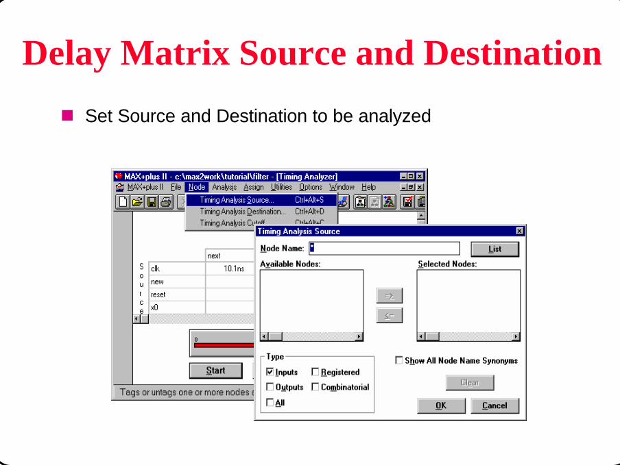
© CIC Altera Max+PlusII Y.T.Chou/Steven Page 240
Delay Matrix Source and Destination
n Set Source and Destination to be analyzed

© CIC Altera Max+PlusII Y.T.Chou/Steven Page 241
Useful Analysis Options
n Time Restrictions– Show All Path– Show Only Longest Paths– Show Only Shortest Paths
n Cell Width– Control matrix display
n Cut Off I/O Pin Feedback– See next page
n Cut Off Clear & Preset Paths– No clear or preset delay analysis
n List Only Longest Path– List Path lists only longest path between two points

© CIC Altera Max+PlusII Y.T.Chou/Steven Page 242
Cut Off I/O Pin Feedback
D Q D Q
AB
C
uUsed to break bi-directional pin from the analysisuWhen on, paths A and B true C falseuWhen off, path A, B and C are true

© CIC Altera Max+PlusII Y.T.Chou/Steven Page 243
Run Delay Matrix Analysis
n Select Delay Matrix Analysis and click on Start buttonn Matrix shows all paths, longest path, or shortest path
depending on Time Restrictions option selectedn Use List Path to analyze the path of delays

© CIC Altera Max+PlusII Y.T.Chou/Steven Page 244
Comb D Q
tsetup, thold
u Setup/Hold Matrix calculates setup & hold times for device flip-flops
u Setup • tsetup = tdata - tclock + tsetup
u Hold• thold = tclock - tdata + thold
Setup/Hold Matrix Analysis
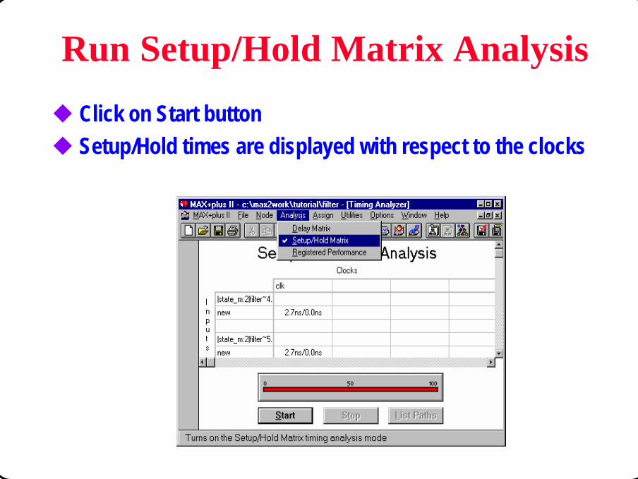
© CIC Altera Max+PlusII Y.T.Chou/Steven Page 245
Run Setup/Hold Matrix Analysis
u Click on Start buttonu Setup/Hold times are displayed with respect to the clocks

© CIC Altera Max+PlusII Y.T.Chou/Steven Page 246
Saving Timing Analysis Results
u Save the current Timing Analyzer results to a TAO File• Timing Analyzer can save the information in the current timing analysis display to an
ASCII-format Timing Analyzer Output file (*.tao)Menu: File -> Save Analysis As...
Destination
y3 y4 y5 ----------------- ----------------- -----------------
S aclr . . . o clk 10.8ns 12.7ns 11.7ns u xin1 . . . r xin2 . . . c xin3 . . . e xin4 . . .
xin5 . . . xin6 . . . xin7 . . . xin8 . . .
© CIC Altera Max+PlusII Y.T.Chou/Steven Page 247
Listing & Locating Delay Paths
u To trace delay paths or clock paths in the design file• After you run a timing analysis, you can list selected signal paths and locate them in
the original design file(s) for the project• Select the matrix cell or clock, click List Paths• Select one of the delay paths shown in Message Processor, and click Locate to
trace the path in the source file(s)
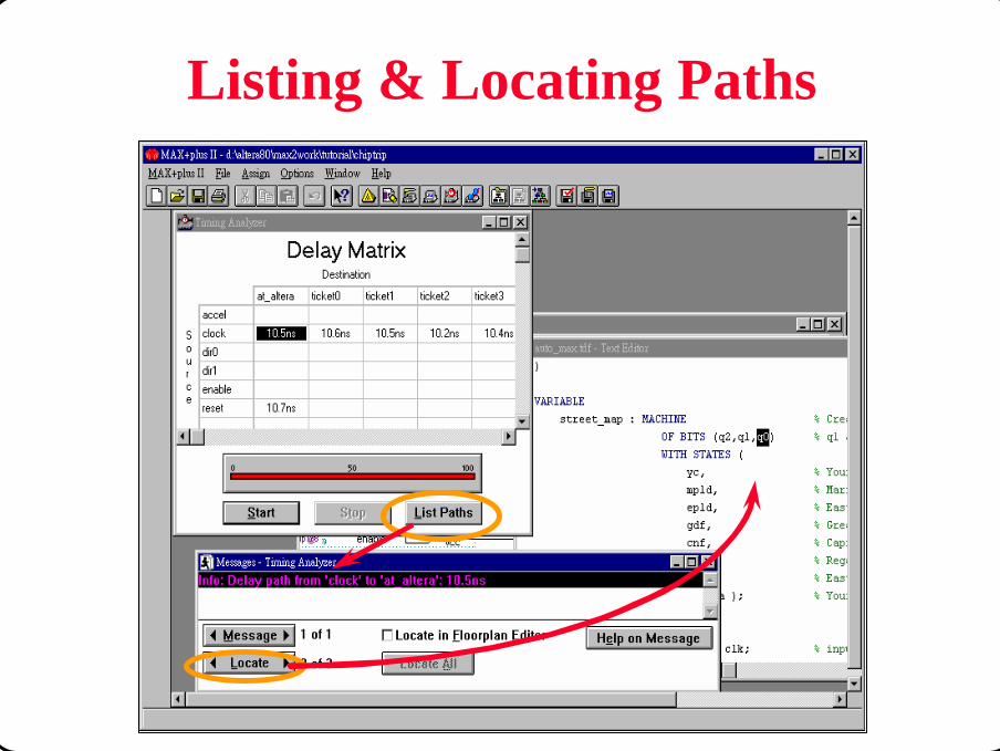
© CIC Altera Max+PlusII Y.T.Chou/Steven Page 248
Listing & Locating Paths

© CIC Altera Max+PlusII Y.T.Chou/Steven Page 249
Recommended Verification Flow
u Functional simulation• Perform functional simulation to verify the design functionality
u Timing Analysis• Perform static timing analysis to check overall performance• Find the delay paths
u Timing simulation• Perform timing simulation to verify real-world design timing & functionality
u On-board test• Program FPGA/CPLD device(s) and test the function & timing in system

© CIC Altera Max+PlusII Y.T.Chou/Steven Page 250
Timing Analysis Recommendations
u Use Timing Analyzer to locate performance bottlenecku Use Registered Performance Analysis to determine
internal clock frequency performance of the designu Use Show Only Longest Path Time Restrictions in Delay
Matrix to get the longest delay time from input pin to output pin
u Use List Path and Locate in Floorplan Editor to view worst case paths
u Use List Path and Locate to trace through path in design file
u Use assignments and recompile to fine-tune performance

© CIC Altera Max+PlusII Y.T.Chou/Steven Page 251
Project Timing Analysis Summary
u Timing Analyzer is a static timing analyzeru Three modes of Timing Analysis
• Registered Performance• Delay Matrix• Setup/Hold Matrix
u Provides ability to trace path through Floorplan Editor or design file
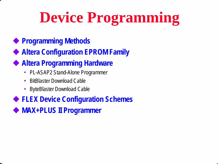
© CIC Altera Max+PlusII Y.T.Chou/Steven Page 252
Device Programmingu Programming Methodsu Altera Configuration EPROM Familyu Altera Programming Hardware
• PL-ASAP2 Stand-Alone Programmer• BitBlaster Download Cable• ByteBlaster Download Cable
u FLEX Device Configuration Schemesu MAX+PLUS II Programmer
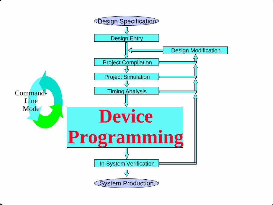
© CIC Altera Max+PlusII Y.T.Chou/Steven Page 253
System Production
Design Specification
Design Entry
Project Compilation
Timing Analysis
In-System Verification
Design Modification
Device Programming
Project Simulation
Command-LineMode
© CIC Altera Max+PlusII Y.T.Chou/Steven Page 254
Altera Provide Method
u Altera provide different methods for • Program Device
– MAX family• Configure Device
– FLEX family
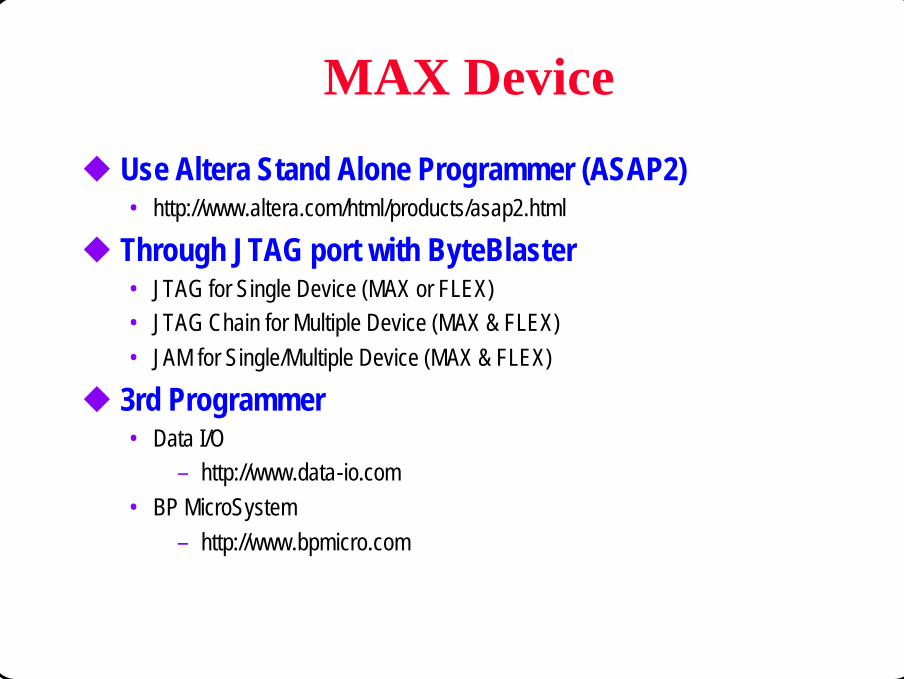
© CIC Altera Max+PlusII Y.T.Chou/Steven Page 255
MAX Device
u Use Altera Stand Alone Programmer (ASAP2)• http://www.altera.com/html/products/asap2.html
u Through JTAG port with ByteBlaster• JTAG for Single Device (MAX or FLEX)• JTAG Chain for Multiple Device (MAX & FLEX)• JAM for Single/Multiple Device (MAX & FLEX)
u 3rd Programmer• Data I/O
– http://www.data-io.com• BP MicroSystem
– http://www.bpmicro.com

© CIC Altera Max+PlusII Y.T.Chou/Steven Page 256
FLEX Device
u Through JTAG port with ByteBlaster• JTAG for Single Device (FLEX or MAX)• JTAG Chain for Multiple Device (FLEX & MAX)
u Through PS port with ByteBlaster• FLEX for Single Device• FLEX Chain for Multiple Device
u Serial PROM• EPC1 (1Mbits, good for 6K/8K/10K)• EPC1441(441Kbits, good for 6K/8K/10K10, 10K20, 10K30)• EPC1213 (213Kbits, only for 8K)• EPC1064 (64Kbits, only for 8K)

© CIC Altera Max+PlusII Y.T.Chou/Steven Page 257
Configuration File Sizes
u FLEX device configuration file sizes• Each FLEX device has a different size requirement for its configuration data, based
on the number of SRAM cells in the device• The following table summarizes the configuration file size required for each FLEX
device– To calculate the amount of data storage space for multi-device configurations,
simply add the file sizes for each FLEX device in the designDevice
EPF8282A/VEPF8452AEPF8636AEPF8820AEPF81188AEPF81500A
Data Size(bits)
40,00064,00096,000
128,000192,000250,000
Device
EPF10K10EPF10K20EPF10K30EPF10K40EPF10K50EPF10K70EPF10K100
Data Size(bits)
115,000225,000368,000488,000609,000881,000
1,172,000

© CIC Altera Max+PlusII Y.T.Chou/Steven Page 258
Altera Configuration EPROM Family
u Altera’s serial configuration EPROMs for FLEX devices• Simple, easy-to-use 4-pin interface to FLEX devices• Available in OTP packages: 8-pin PDIP, 20-pin PLCC and 32-pin TQFP• Family member
– EPC1064: 65,536 bit device with 5.0-V operation– EPC1064V: 65,536 bit device with 3.3-V operation– EPC1213: 212,942 bit device with 5.0-V operation– EPC1: 1,046,496 bit device with 5.0-V or 3.3-V operation
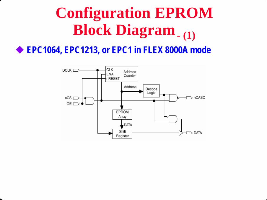
© CIC Altera Max+PlusII Y.T.Chou/Steven Page 259
Configuration EPROMBlock Diagram - (1)
u EPC1064, EPC1213, or EPC1 in FLEX 8000A mode

© CIC Altera Max+PlusII Y.T.Chou/Steven Page 260
Configuration EPROMBlock Diagram - (2)
u EPC1 in FLEX 10K mode
Internal oscillator

© CIC Altera Max+PlusII Y.T.Chou/Steven Page 261
Altera Programming Hardware
u Hardware to program and configure Altera devices• For MAX 7000/E/S, MAX 9000 and Altera configuration EPROM(EPC- series)
devices– Altera stand-alone programmer: PL-ASAP2 (PC platform)– 3rd-party universal programmer (PC platform)
• For MAX 7000S and MAX 9000 ISP, FLEX devices downloading– Altera BitBlaster download cable (RS-232 port)– Altera ByteBlaster download cable (parallel port of PC)
• Of course, you can use another 3rd-party universal programmer or download cable to program or configure Altera devices. In this chapter, we discuss Altera programming hardware only.
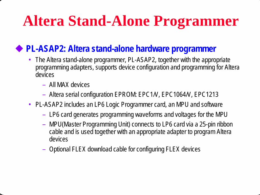
© CIC Altera Max+PlusII Y.T.Chou/Steven Page 262
Altera Stand-Alone Programmer
u PL-ASAP2: Altera stand-alone hardware programmer• The Altera stand-alone programmer, PL-ASAP2, together with the appropriate
programming adapters, supports device configuration and programming for Altera devices
– All MAX devices– Altera serial configuration EPROM: EPC1/V, EPC1064/V, EPC1213
• PL-ASAP2 includes an LP6 Logic Programmer card, an MPU and software– LP6 card generates programming waveforms and voltages for the MPU– MPU(Master Programming Unit) connects to LP6 card via a 25-pin ribbon
cable and is used together with an appropriate adapter to program Altera devices
– Optional FLEX download cable for configuring FLEX devices

© CIC Altera Max+PlusII Y.T.Chou/Steven Page 263
Installing LP6 Card, MPU & Adapter
LP6 Programmer Card
MPU Base Unit
Adapter
Connect the 25-pin flat ribbon cable to the LP6 card
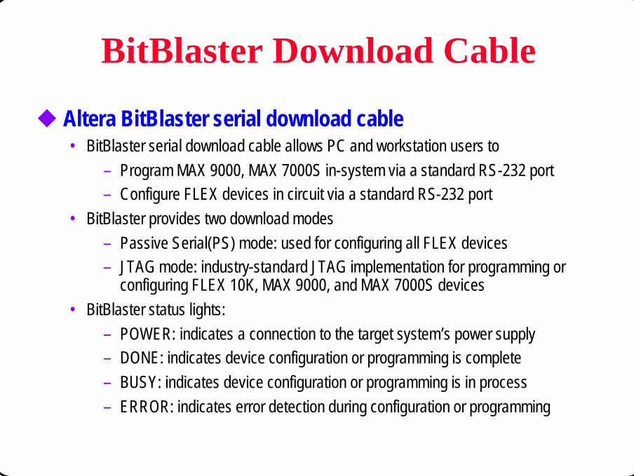
© CIC Altera Max+PlusII Y.T.Chou/Steven Page 264
BitBlaster Download Cable
u Altera BitBlaster serial download cable• BitBlaster serial download cable allows PC and workstation users to
– Program MAX 9000, MAX 7000S in-system via a standard RS-232 port– Configure FLEX devices in circuit via a standard RS-232 port
• BitBlaster provides two download modes– Passive Serial(PS) mode: used for configuring all FLEX devices– JTAG mode: industry-standard JTAG implementation for programming or
configuring FLEX 10K, MAX 9000, and MAX 7000S devices• BitBlaster status lights:
– POWER: indicates a connection to the target system’s power supply– DONE: indicates device configuration or programming is complete– BUSY: indicates device configuration or programming is in process– ERROR: indicates error detection during configuration or programming

© CIC Altera Max+PlusII Y.T.Chou/Steven Page 265
Installing BitBlaster

© CIC Altera Max+PlusII Y.T.Chou/Steven Page 266
ByteBlaster Download Cable
u Altera ByteBlaster parallel port download cable• ByteBlaster serial download cable allows PC users to
– Program MAX 9000, MAX 7000S in-system via a standard parallel port– Configure FLEX devices in circuit via a standard parallel port
• ByteBlaster provides two download modes– Passive Serial(PS) mode: used for configuring all FLEX devices– JTAG mode: industry-standard JTAG implementation for programming or
configuring FLEX 10K, MAX 9000, and MAX 7000S devices• ByteBlaster download cable provides a fast and low-cost method for ISP and FLEX
device configuration• ByteBlaster download cable uses identical 10-pin circuit board connector as the
BitBlaster serial download cable

© CIC Altera Max+PlusII Y.T.Chou/Steven Page 267
Installing ByteBlaster

© CIC Altera Max+PlusII Y.T.Chou/Steven Page 268
BitBlaster & ByteBlasterPlug Connections
Pin
12345678910
PS Mode
DCLKGNDCONF_DONEVCCnCONFIGN.C.nSTATUSN.C.DATA0GND
JTAG Mode
TCKGNDTDOVCCTMSN.C.N.C.N.C.TDIGND

© CIC Altera Max+PlusII Y.T.Chou/Steven Page 269
FLEX Device Configuration Schemes
u Passive Serial(PS) configuration with the download cable• Single-device configuration• Multiple-devices configuration
u JTAG configuration with the download cable• Available for FLEX 10K and ISP devices only
u Serial configuration EPROM configuration• FLEX 8000A Active Serial(AS) configuration with serial configuration EPROM• FLEX 10K Passive Serial(PS) configuration with EPC1 configuration EPROM
u Parallel EPROM configuration• FLEX 8000A Active Parallel Up(APU) or Active Parallel Down(APD) configuration• Not available for FLEX 10K devices

© CIC Altera Max+PlusII Y.T.Chou/Steven Page 270
FLEX 8000A Single-Device PS Configuration with the Download Cable

© CIC Altera Max+PlusII Y.T.Chou/Steven Page 271
FLEX 8000A Multiple-Device PS Configuration with the Download Cable
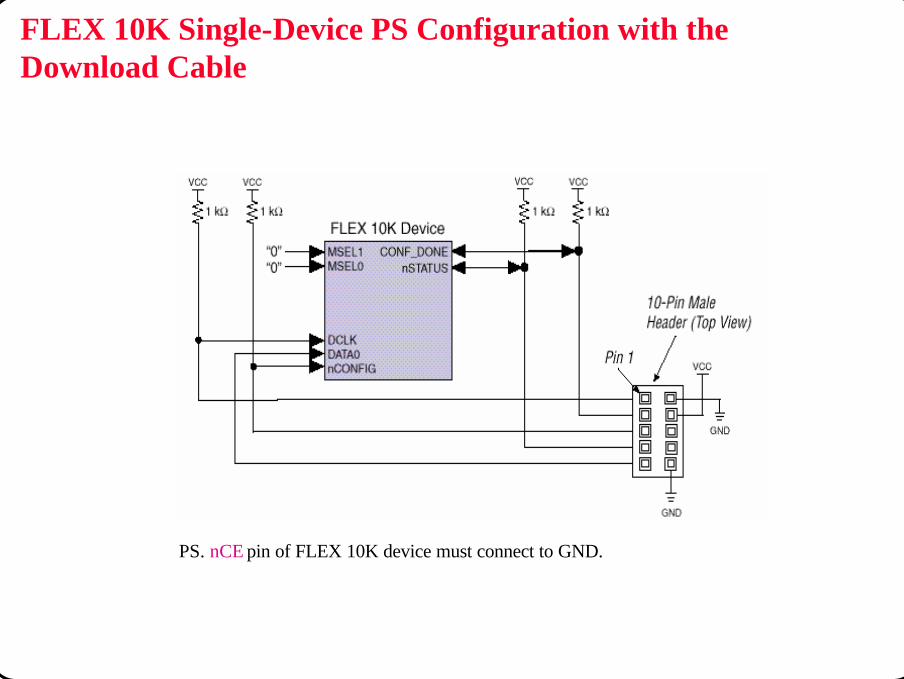
© CIC Altera Max+PlusII Y.T.Chou/Steven Page 272
PS. nCE pin of FLEX 10K device must connect to GND.
FLEX 10K Single-Device PS Configuration with the Download Cable

© CIC Altera Max+PlusII Y.T.Chou/Steven Page 273
PS. nCE pin of the lead FLEX 10Kdevice must connect to GND.
FLEX 10K Multiple-Device PS Configuration with the Download Cable

© CIC Altera Max+PlusII Y.T.Chou/Steven Page 274
JTAG Configuration with the Download Cable
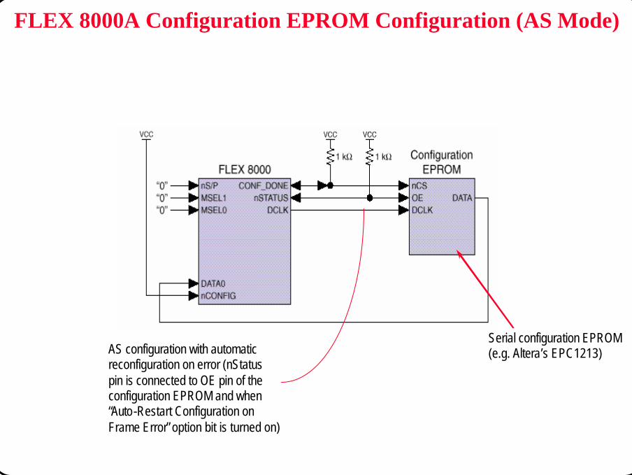
© CIC Altera Max+PlusII Y.T.Chou/Steven Page 275
FLEX 8000A Configuration EPROM Configuration (AS Mode)
Serial configuration EPROM(e.g. Altera’s EPC1213)AS configuration with automatic
reconfiguration on error (nStatuspin is connected to OE pin of theconfiguration EPROM and when“Auto-Restart Configuration onFrame Error”option bit is turned on)
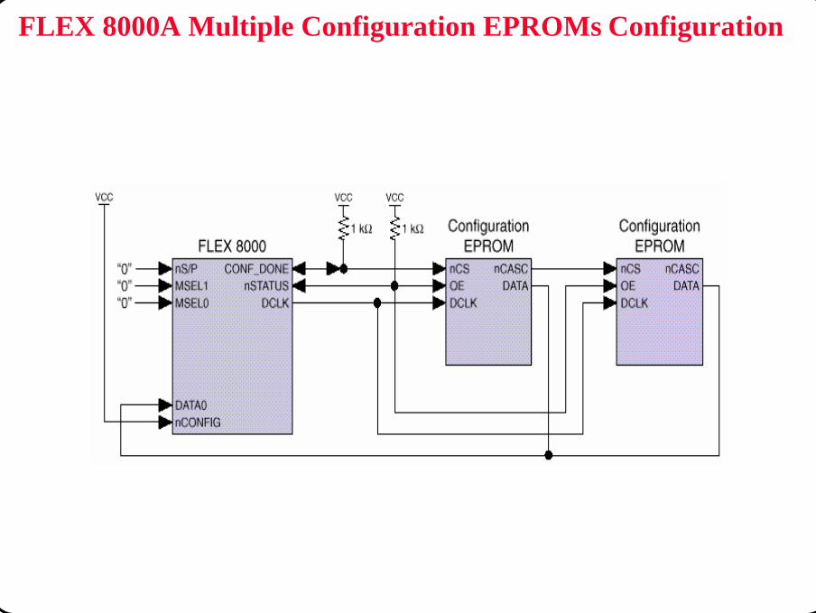
© CIC Altera Max+PlusII Y.T.Chou/Steven Page 276
FLEX 8000A Multiple Configuration EPROMs Configuration

© CIC Altera Max+PlusII Y.T.Chou/Steven Page 277
FLEX 8000A Multi-Device Configuration EPROM Configuration
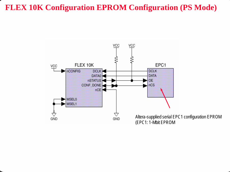
© CIC Altera Max+PlusII Y.T.Chou/Steven Page 278
FLEX 10K Configuration EPROM Configuration (PS Mode)
Altera-supplied serial EPC1 configuration EPROM(EPC1: 1-Mbit EPROM

© CIC Altera Max+PlusII Y.T.Chou/Steven Page 279
FLEX 10K Multi-Device Configuration EPROM Configuration

© CIC Altera Max+PlusII Y.T.Chou/Steven Page 280
FLEX 8000A APU & APD Configuration

© CIC Altera Max+PlusII Y.T.Chou/Steven Page 281
FLEX 8000A Multi-Device APU & APD Configuration

© CIC Altera Max+PlusII Y.T.Chou/Steven Page 282
MAX+PLUS II Programmer
u To program or configure Altera devices• After the MAX+PLUS II Compiler has processed a
project, it generates one or more programming files, which the Programmer uses to program or configure one or more devices
• The MAX+PLUS II Programmer allows you to program, verify, examine, blank-check, configure, and test Altera all MAX and FLEX devices and configuration EPROM
• With the Programmer and programming hardware--the Altera MPU, add-on cards, programming adapters, the FLEX download cable, the BitBlaster, or the ByteBlaster--you can easily create a working device in minutes

© CIC Altera Max+PlusII Y.T.Chou/Steven Page 283
Device Programming Methodology
.plf
.hex
.pofMAX+PLUS IIProgrammer
MasterProgrammingUnit (MPU)
.jed
.sof
AlteraCPLD
.pof
.jed
.ttf.sbf
.scf .vec
BitBlasterDownload
Cable
(PC)
(PC/WS)
ByteBlasterDownload
Cable
(PC)

© CIC Altera Max+PlusII Y.T.Chou/Steven Page 284
Programmer Operations
u 6 operations• Program : programs data onto a blank MAX device or configuration EPROM• Verify : verifies contents of a device against current programming data• Examine : examines a device & stores the data in a temporary buffer• Blank-Check : examines a device to ensure it is blank• Test : functionally tests a programmed device• Configure: downloads configuration data into the SRAM of one or more FLEX
devices
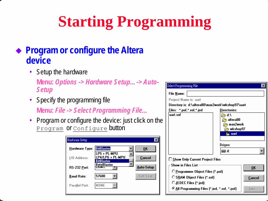
© CIC Altera Max+PlusII Y.T.Chou/Steven Page 285
Starting Programming
u Program or configure the Altera device
• Setup the hardwareMenu: Options -> Hardware Setup... -> Auto-Setup
• Specify the programming fileMenu: File -> Select Programming File...
• Program or configure the device: just click on the Program or Configure button
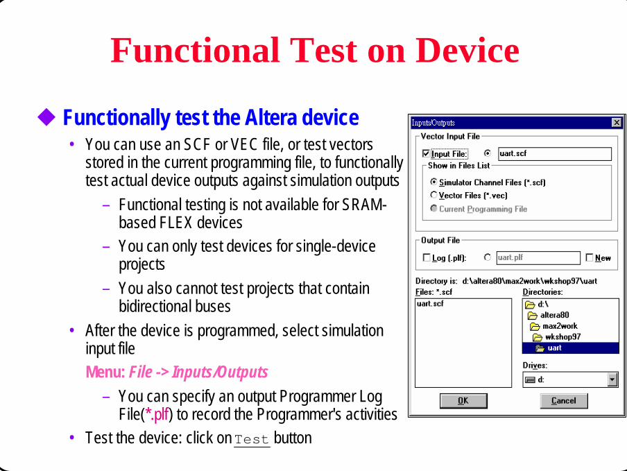
© CIC Altera Max+PlusII Y.T.Chou/Steven Page 286
Functional Test on Device
u Functionally test the Altera device• You can use an SCF or VEC file, or test vectors
stored in the current programming file, to functionally test actual device outputs against simulation outputs
– Functional testing is not available for SRAM-based FLEX devices
– You can only test devices for single-device projects
– You also cannot test projects that contain bidirectional buses
• After the device is programmed, select simulation input fileMenu: File -> Inputs/Outputs
– You can specify an output Programmer Log File(*.plf) to record the Programmer's activities
• Test the device: click on Test button
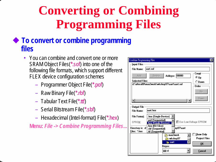
© CIC Altera Max+PlusII Y.T.Chou/Steven Page 287
Converting or Combining Programming Files
u To convert or combine programming files
• You can combine and convert one or moreSRAM Object Files(*.sof) into one of thefollowing file formats, which support differentFLEX device configuration schemes
– Programmer Object File(*.pof)– Raw Binary File(*.rbf)– Tabular Text File(*.ttf)– Serial Bitstream File(*.sbf)– Hexadecimal (Intel-format) File(*.hex)
Menu: File -> Combine Programming Files...

© CIC Altera Max+PlusII Y.T.Chou/Steven Page 288
Configuring Multiple FLEX Devices
u Configure multiple FLEX device with the download cable• You can configure multiple FLEX devices in a FLEX chain with the download cable
– By typing a command at a DOS command prompt to download configuration data from an SBF file through the BitBlasterDOS Prompt: copy <design>.sbf COM1: (or COM2:)
• The SBF file can be created by using “Combine Programming File”command (under File Menu)
– By creating “multi-device FLEX chain”(under FLEX Menu) and using the Programmer to download configuration data from SOFs through the BitBlaster, ByteBlaster, or FLEX download cable
• Multi-device FLEX chain: a series of FLEX devices through which configuration data is passed from device to device using the sequential Passive Serial configuration scheme
FLEX Menu
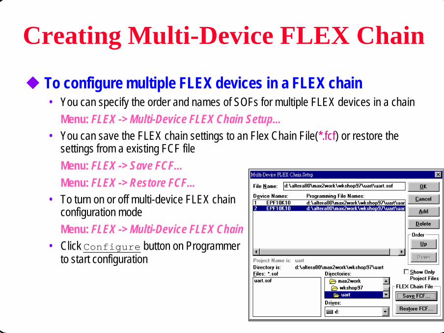
© CIC Altera Max+PlusII Y.T.Chou/Steven Page 289
Creating Multi-Device FLEX Chain
u To configure multiple FLEX devices in a FLEX chain• You can specify the order and names of SOFs for multiple FLEX devices in a chain
Menu: FLEX -> Multi-Device FLEX Chain Setup...• You can save the FLEX chain settings to an Flex Chain File(*.fcf) or restore the
settings from a existing FCF fileMenu: FLEX -> Save FCF...Menu: FLEX -> Restore FCF...
• To turn on or off multi-device FLEX chainconfiguration modeMenu: FLEX -> Multi-Device FLEX Chain
• Click Configure button on Programmerto start configuration

© CIC Altera Max+PlusII Y.T.Chou/Steven Page 290
Programming Multiple JTAG Devices
u Program or configure multiple JTAG devices with the download cable
• You can program or configure one or more MAX 9000, MAX 7000S, FLEX 10K devices, and other devices that support JTAG programming in a JTAG chain using the BitBlaster or ByteBlaster
– The JTAG chain can contain any combination of Altera and non-Altera devices that comply with the IEEE 1149.1 JTAG specification, including some FLEX 8000 devices
– By creating “multi-device JTAG chain”(under JTAG Menu) and using the Programmer to download configuration data from SOFs through the BitBlasteror ByteBlaster cable
• Multi-device JTAG chain: a series of devices through which programming and/or configuration data are passed from device to device via the JTAG boundary-scan test circuitry
JTAG Menu
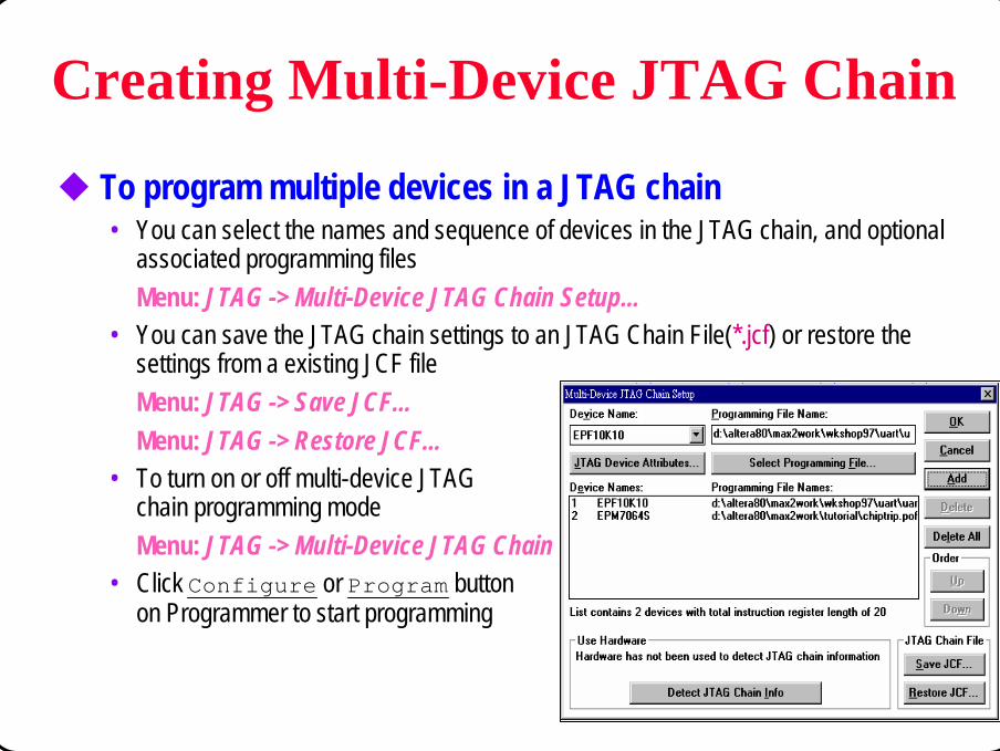
© CIC Altera Max+PlusII Y.T.Chou/Steven Page 291
Creating Multi-Device JTAG Chain
u To program multiple devices in a JTAG chain• You can select the names and sequence of devices in the JTAG chain, and optional
associated programming filesMenu: JTAG -> Multi-Device JTAG Chain Setup...
• You can save the JTAG chain settings to an JTAG Chain File(*.jcf) or restore the settings from a existing JCF fileMenu: JTAG -> Save JCF...Menu: JTAG -> Restore JCF...
• To turn on or off multi-device JTAGchain programming modeMenu: JTAG -> Multi-Device JTAG Chain
• Click Configure or Program buttonon Programmer to start programming

© CIC Altera Max+PlusII Y.T.Chou/Steven Page 292
Details about Device Programming
u Please refer to Altera document for details• Altera Data Book• Altera Data Sheet
– dsconf_06.pdf: Configuration EPROMs for FLEX Devices– dsbit03.pdf: BitBlaster Serial Download Cable– dsbyte01.pdf: ByteBlaster Parallel Port Download Cable
• Altera Application Note & Application Brief– an033_03.pdf: Configuring FLEX 8000 Devices– an038_03.pdf: Configuring FLEX 8000 Devices– an059_01.pdf: Configuring FLEX 10K Devices– ab141_01.pdf: In-System Programmability in MAX 9000 Devices– ab145_01.pdf: Designing for In-System Programmability in MAX 7000S Devices– an039_03.pdf: JTAG Boundary Scan Testing in Altera Devices

© CIC Altera Max+PlusII Y.T.Chou/Steven Page 293
uCIC technical support : Steven / 周育德• Phone : (03)5773693 ext. 148• Email : [email protected]• WWW : http://www.cic.edu.tw/chip_design/design_intr/altera/
To buy Altera chips, hardware or demo boards:• Contact Galaxy Far East Corp. 茂綸股份有限公司周怡慧 小姐電話: (02) 2705-7266 # 108 [email protected]
u Altera technical support on Internet• WWW : http://www.altera.com
Getting Help