
Alma Mater Studiorum – Università di Bologna Dipartimento...
85
Alma Mater Studiorum – Università di Bologna Dipartimento di Ingegneria dell'Energia Elettrica e dell'Informazione Dottorato di Ricerca in Ingegneria Elettrotecnica Ciclo XXVI Settore Concorsuale di afferenza: 09/E1 Settore Scientifico disciplinare: ING-IND/31 ARBITRARY WAVEFORM MULTILEVEL GENERATOR FOR HIGH VOLTAGE HIGH FREQUENCY PLASMA ACTUATORS di Filopimin Andreas Dragonas Tutor: Gabriele Grandi Coordinatore: Domenico Casadei Co-Tutor: Gabriele Neretti Anno Esame Finale 2014
Transcript of Alma Mater Studiorum – Università di Bologna Dipartimento...

Alma Mater Studiorum – Università di Bologna
Dipartimento di Ingegneria dell'Energia Elettrica e dell'Informazione
Dottorato di Ricerca in Ingegneria Elettrotecnica
Ciclo XXVI
Settore Concorsuale di afferenza: 09/E1
Settore Scientifico disciplinare: ING-IND/31
ARBITRARY WAVEFORM MULTILEVEL GENERATOR
FOR HIGH VOLTAGE HIGH FREQUENCY
PLASMA ACTUATORS
di
Filopimin Andreas Dragonas
Tutor: Gabriele Grandi Coordinatore: Domenico Casadei
Co-Tutor: Gabriele Neretti
Anno Esame Finale 2014

i
Preface
This dissertation presents the theory and the
conducted activity that lead to the construction of a high voltage
high frequency arbitrary waveform voltage generator. The
generator has been specifically designed to supply power to a
wide range of plasma actuators. The system has been
completely designed, manufactured and tested at the
Department of Electrical, Electronic and Information Engineering
of the University of Bologna.
The generator structure is based on the single phase
cascaded H-bridge multilevel topology and is comprised of 24
elementary units that are series connected in order to form the
typical staircase output voltage waveform of a multilevel
converter. The total number of voltage levels that can be
produced by the generator is 49. Each level is 600 V making the
output peak-to-peak voltage equal to 28.8 kV. The large number
of levels provides high resolution with respect to the output
voltage having thus the possibility to generate arbitrary
waveforms. Maximum frequency of operation is 20 kHz.
A study of the relevant literature shows that this is the
first time that a cascaded multilevel converter of such
dimensions has been constructed. Isolation and control
challenges had to be solved for the realization of the system.
The biggest problem of the current technology in
power supplies for plasma actuators is load matching. Resonant
converters are the most used power supplies and are seriously
affected by this problem. The manufactured generator
completely solves this issue providing consistent voltage output

ii
independently of the connected load. This fact is very important
when executing tests and during the comparison of the results
because all measures should be comparable and not dependent
on matching issues.
The use of the multilevel converter for power
supplying a plasma actuator is a real technological breakthrough
that has provided and will continue to provide very significant
experimental results.
The importance of the generator has been noticed by
the aerospace company Alenia Aermacchi (AAM) that has
shown interest in the project. During the last year collaboration
between our department and AAM was started. Lab tests were
conducted in partnership with AAM technicians both at the
university as well as at the AAM headquarters. The experimental
results showed the great potential of the implemented
technology.
Finally, it is a pleasure to mention that AAM was
highly convinced by this potential and funded a project for the
construction of new generator that is based on the work
presented in this dissertation.

iii
Acknowledgements
I would like to express my sincere gratitude to my
tutor, Gabriele Grandi for the technical support he has provided
through these years.
I’m also thankful to the Lisp lab team headed by
professor Carlo Angelo Borghi. A particular thank you to
Gabriele Neretti.
Finally, I thank my fantastic parents for supporting me
all these years and my beautiful baby for putting up with me
through the difficult times and bringing joy to my life every day.
Love you.

iv
Table of Contents
Preface ....................................................................... i
Acknowledgements ................................................... iii
List of Figures ........................................................... vi
Chapter 1 .................................................................. 1
Introduction ............................................................ 1
1.1 Plasma....................................................... 1
1.2 Dielectric Barrier Discharge ....................... 3
1.3 Active Flow Control .................................... 5
1.4 Power Supplies .........................................13
1.5 Multilevel Converters ................................14
1.5.1 Diode Clamped ......................................15
1.5.2 Capacitor Clamped ................................16
1.5.3 Cascaded Multilevel ..............................17
Chapter 2 .................................................................19
System implementation: Hardware .......................19
2.1 Project Design ..........................................19
2.2 Batteries and Isolation ..............................21
2.3 The Flyback Converter .............................23
2.3.1 Operation of the Flyback .......................24
2.3.2 Designing the Flyback ...........................26
2.4 The DC/AC stage .....................................32
2.5 PCB Overview ..........................................33
Chapter 3 .................................................................41
system implementation: software and control .......41

v
3.1 Control Method .........................................41
3.2 The control unit .........................................43
3.3 Simulations ...............................................46
3.4 Input power balancing ..............................52
3.5 Cycling Levels ..........................................53
3.6 Dynamic Balancing ...................................56
Chapter 4 .................................................................59
Experimental results .............................................59
4.1 17 levels vs sinusoidal ..............................59
4.2 Full voltage tests .......................................61
4.2.1 Square waveform ..................................62
4.2.2 Triangular Waveform .............................66
4.2.3 Sawtooth................................................67
4.2.4 Semi sinusoidal .....................................69
4.2.5 Positive triangle .....................................70
4.3 Velocity measures ....................................71
Chapter 5 .................................................................74
Conclusions ..........................................................74
References ...............................................................75

vi
List of Figures
Figure 1.1 A plasma lamp .. 1
Figure 1.2 Electrons and positive Ions .. 2
Figure 1.3 The DBD configuration .. 4
Figure 1.4 Flow Separation .. 7
Figure 1.5 The stall phenomenon .. 8
Figure 1.6 Spoilers on a wing .. 9
Figure 1.7 A plasma actuator .. 11
Figure 1.8 Formation of plasma .. 12
Figure 1.9 Typical multilevel staircase .. 15
Figure 1.10 Diode clamped topology .. 16
Figure 1.11 Capacitor clamped topology .. 18
Figure 1.12 Cascaded H-bridge topology .. 19
Figure 2.1 Schematic view of the multilevel converter .. 21
Figure 2.2 Short-circuit situation .. 22
Figure 2.3 Flyback converter .. 24
Figure 2.4 Flyback waveforms .. 26
Figure 2.5 Flyback LTspice schematic .. 30
Figure 2.6 Simulated output voltage of the flyback .. 31
Figure 2.7 Simulated current at start phase .. 32
Figure 2.8 Simulated current end phase .. 32
Figure 2.9 Integrated power module .. 33
Figure 2.10 Orcad schematic of the flyback part .. 36
Figure 2.11 Orcad schematic of the inverter part .. 38
Figure 2.12 Manufactured elementary unit: top .. 39
Figure 2.13 Manufactured elementary unit: Bottom .. 40
Figure 2.14 Stack of 8 elementary units .. 40
Figure 2.15 Complete system .. 41

vii
Figure 3.1 Multilevel waveform .. 43
Figure 3.2 Arduino MCU .. 44
Figure 3.3 Simulink model of the total system .. 47
Figure 3.4 Waveform formation .. 48
Figure 3.5 Elementary unit model .. 49
Figure 3.6 Driver model .. 49
Figure 3.7 H-bridge model .. 50
Figure 3.8 Simulated output voltage waveform .. 51
Figure 3.9 Simulated output current .. 52
Figure 3.10 Detailed view of V1 and V24 .. 53
Figure 3.11 Cycling levels model .. 55
Figure 3.12 Cycling levels waveforms .. 56
Figure 3.13 Dynamic balancing model .. 57
Figure 3.14 Windowed integrator .. 58
Figure 4.1 Triangular waveform .. 61
Figure 4.2 Sine waveform .. 61
Figure 4.3 Square waveform .. 65
Figure 4.4 Detailed view of the voltage and the current .. 66
Figure 4.6 Triangular waveform .. 67
Figure 4.7 Simulated triangular waveform .. 68
Figure 4.8 Sawtooth waveform .. 69
Figure 4.9 Simulated sawtooth waveform .. 69
Figure 4.10 Semi sinusoidal waveform .. 70
Figure 4.11 Sine waveform .. 71
Figure 4.12 Positive triangular waveform .. 72
Figure 4.13 Velocity starting at 12 mm .. 73
Figure 4.14 Velocity starting at 20 mm .. 74

1
Chapter 1
INTRODUCTION
1.1 Plasma
Figure 1.1 A plasma lamp
Plasma (Fig. 1.1) in physics is often defined as the
fourth fundamental state of matter with regard to the other three
being solid, liquid and gas. A solid substance at constant
pressure is generally transformed into liquid by increasing its
temperature. Following the same principle by further increasing
the temperature a liquid becomes a gas. At a sufficiently high
temperature the molecules of the gas decompose forming a
cloud of atoms that move independently in casual directions. By
increasing the temperature even more the atoms break down

2
into freely moving charged particles, which are electrons and
positive ions. When this event triggers the substance is said to
have entered the plasma state.
Figure 1.2 Electrons and positive Ions
Although it is the least familiar state of matter for us,
inhabitants of planet Earth, plasma is actually the most common
state of matter throughout the whole visible universe. Based on
the thermodynamic equilibrium state of which the plasma is in, it
is divided into two principal categories:
• Thermal plasma, where the heavy charge species like
ions often have the same temperature as the electrons;
• Non-thermal plasma, where the electrons’ temperature is
much higher than that of the heavy charge species.
Thermal plasmas can be for example arcs or radio
frequency inductively coupled plasma discharges. They are
associated with Joule heating and thermal ionization, and
usually occur at high pressure. The temperature can reach
around 4,000K to 30,000K. The applications of thermal plasmas

3
include metal cutting and welding, metal spraying and waste
incineration.
When non-thermal plasmas are being produced, the
majority of the electrical energy mainly goes into the generations
of energetic electrons while the rest of the gas remains at low
temperature. Thus, the electron temperature reaches around
105 K. In the meantime ions and neutral species are at room
temperature. Thus, non-thermal plasmas can be generated at
low pressure and low temperature circumstances. Non-thermal
plasma is the subject of this dissertation.
1.2 Dielectric Barrier Discharge
The dielectric barrier discharge [DBD] is a suitable
way to generate a stable, confined and homogeneous plasma at
high as well as at atmospheric pressure. This method was first
introduced in 1857 by Ernst Werner von Siemens for generating
ozone.
In order to achieve a DBD appropriate AC voltage has
to be applied between two electrodes that are first separated by
an insulating material. Fig. 1.3 depicts a schematic DBD setup.
Typical voltage levels for these devices are in orders of kV and
are usually applied to only one of the two electrodes. The other
is anchored to the ground potential. The dielectric material plays
a significant role in the formation of the plasma and its quality.
Typical materials for this use are polymers such as Kapton and
Teflon or even Plexiglas.

As depicted in the figure plasma is established
directly in the shape of streamer channels, i.e. arcs, and no
sparks are formed. This phenomenon
is due to the accumulation of charged species on the dielectric
layer that limit the electric field in the gas gap and so the lifespan
of the microdischarges cannot exceed few hundreds of
nanoseconds.
The use of DC voltages is ob
existence of a separating dielectric layer and DBD is usually
operated at high frequencies that range from few kHz to even
thousands of kHz.
is currently being experimented in different resea
industrial processes
particles that coexist with high energetic electrons and reactive
radicals, make this type of plasma very attractive for engineering
purposes. Typical plasma uses are:
• plasma
• surface treatment to increase dyeability, wettability and
adhesion
Figure 1.3 The DBD configuration
As depicted in the figure plasma is established
directly in the shape of streamer channels, i.e. arcs, and no
sparks are formed. This phenomenon is very characteristic and
is due to the accumulation of charged species on the dielectric
layer that limit the electric field in the gas gap and so the lifespan
of the microdischarges cannot exceed few hundreds of
nanoseconds.
The use of DC voltages is obviously excluded by the
existence of a separating dielectric layer and DBD is usually
operated at high frequencies that range from few kHz to even
thousands of kHz. The non-thermal plasma produced by a DBD
being experimented in different research fields and
processes. The relative low temperature of heavy
that coexist with high energetic electrons and reactive
radicals, make this type of plasma very attractive for engineering
Typical plasma uses are:
plasma etching in microelectronics;
surface treatment to increase dyeability, wettability and
adhesion;
4
As depicted in the figure plasma is established
directly in the shape of streamer channels, i.e. arcs, and no
is very characteristic and
is due to the accumulation of charged species on the dielectric
layer that limit the electric field in the gas gap and so the lifespan
of the microdischarges cannot exceed few hundreds of
viously excluded by the
existence of a separating dielectric layer and DBD is usually
operated at high frequencies that range from few kHz to even
thermal plasma produced by a DBD
rch fields and
The relative low temperature of heavy
that coexist with high energetic electrons and reactive
radicals, make this type of plasma very attractive for engineering
surface treatment to increase dyeability, wettability and

5
• sterilization of surfaces and gases from bacteria,
parasites and molds;
• abatement of pollutants and volatile organic compounds
present in combustion processes and cooking activities;
• ozone production;
• food treatment by using pulsed electric fields (PEF) and
non-thermal pasteurization;
• plasma biology and plasma medicine for skin, teeth and
wounds treatment;
• electro-fluid-dynamic actuators for active flow control.
1.3 Active Flow Control
Active flow control is defined as a way of varying the
direction of a flow in order to obtain a desired change. Active
flow control is usually applied to affect three types of situation:
• the laminar-to-turbulent transition,
• the separation,
• and the turbulence;
If the laminar to turbulent transition is delayed the
effect can be that of reduced drag, which for an aircraft can
mean the reduction of the fuel consumption which would lead to
longer range and higher travel speed. The main limitation for the
maximum achievable lift of a curved airfoil is the separation. The
ability of the flow to travel along the shape of the airfoil
determines the moment when the separation occurs. Finally the
decrease in turbulence can significantly reduce the aerodynamic
noise.

6
When a fluid flows along a solid surface of an object,
most of the times the system is studied by separating it into two
distinctive parts: a free stream flow at a certain distance from the
surface and a boundary layer close to the surface. Usually, the
prime boundary layer will be laminar with smooth streamlines.
As the fluid moves further downstream the Reynolds number
which is a function of the development length increases and at
some point transition from laminar to turbulent happens. The
point where the transition occurs depends on many factors
which include the shape of the surface, the level of turbulence in
the free stream flow, and the pressure gradient along the
surface. One important way of characterizing this external flow is
the dimensionless Reynolds number:
=
Where ρ is fluid density, ν is flow velocity, µ is the
dynamic viscosity of the fluid and L is the characteristic length of
the object.
In function of the shape of the surface, there might be
a positive or negative pressure gradient in the boundary layer on
the surface. The positive gradient is known as an adverse
pressure gradient and leads the flow to separate from the
surface. As shown in Fig. 1.4 flow separation happens when the
speed in the boundary layer is highly reduced or even zeroed,
which significantly increases the drag on the surface.
Flow separation can happen both in laminar as well
as in turbulent boundary layers. Turbulent boundary layer has

more momentum near the surface than the laminar bou
layer, this makes it more difficult to slow the boundary flow down
to the separation speed (close to zero). In the low pressure
turbine stage of a jet engine, the flow is fully attached to the
airfoils during takeoff and landing. However, at cruising altitudes
the Reynolds number decreases to the order of 105 because of
the reduced gas density. Part of the flow than becomes laminar
can separate early on the blades, and it then
separated over the rest of the surface. This phenomenon is
usually called the “separation bubble”. Separation makes the
turbine highly inefficient. However, if the laminar
transition happens before the separation point, the bubble can
be majorly limited. For long distance travels, the high loss of
efficiency by separation will can become an important factor on
fuel efficiency. Thus flow separation must be limited in order to
obtain more economic and environmental acute flights.
Separation can also produce flow instabilities behind
bodies of an airfoil or turbine blades. These instabilities generate
high amounts of noise. A
more momentum near the surface than the laminar bou
layer, this makes it more difficult to slow the boundary flow down
the separation speed (close to zero). In the low pressure
turbine stage of a jet engine, the flow is fully attached to the
airfoils during takeoff and landing. However, at cruising altitudes
the Reynolds number decreases to the order of 105 because of
reduced gas density. Part of the flow than becomes laminar
can separate early on the blades, and it then can reattach or be
separated over the rest of the surface. This phenomenon is
usually called the “separation bubble”. Separation makes the
hly inefficient. However, if the laminar-to
transition happens before the separation point, the bubble can
be majorly limited. For long distance travels, the high loss of
efficiency by separation will can become an important factor on
ency. Thus flow separation must be limited in order to
obtain more economic and environmental acute flights.
Separation can also produce flow instabilities behind
bodies of an airfoil or turbine blades. These instabilities generate
high amounts of noise. Active flow control to limit the noise
Figure 1.4 Flow Separation
7
more momentum near the surface than the laminar boundary
layer, this makes it more difficult to slow the boundary flow down
the separation speed (close to zero). In the low pressure
turbine stage of a jet engine, the flow is fully attached to the
airfoils during takeoff and landing. However, at cruising altitudes
the Reynolds number decreases to the order of 105 because of
reduced gas density. Part of the flow than becomes laminar
can reattach or be
separated over the rest of the surface. This phenomenon is
usually called the “separation bubble”. Separation makes the
to-turbulent
transition happens before the separation point, the bubble can
be majorly limited. For long distance travels, the high loss of
efficiency by separation will can become an important factor on
ency. Thus flow separation must be limited in order to
obtain more economic and environmental acute flights.
Separation can also produce flow instabilities behind
bodies of an airfoil or turbine blades. These instabilities generate
ctive flow control to limit the noise
production has been proved effective on a landing
and in the jet engine exhaust.
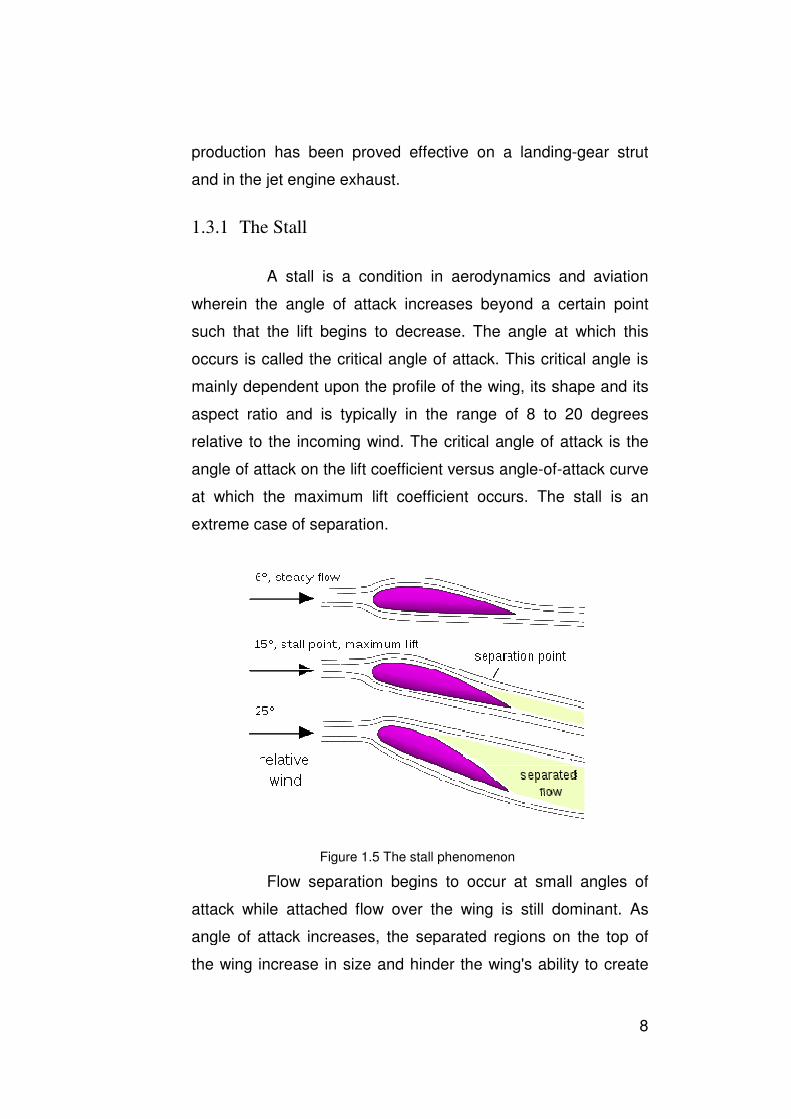
1.3.1 The Stall
A stall is a condition in aerodynamics and aviation
wherein the angle of attack increases beyond a certain point
such that the lift begins to decrease. The angle at which this
occurs is called the critical angle of attack. This critical
mainly dependent upon the profile of the wing, its shape and its
aspect ratio and is typically in the range of 8 to 20 degrees
relative to the incoming wind. The critical angle of attack is the
angle of attack on the lift coefficient versus angle
at which the maximum lift coefficient occurs.
extreme case of separation.
Flow separation begins to occur at small angles of
attack while attached flow over the wing is still dominant. As
angle of attack increases, the separated regions on the top of
the wing increase in size and hinder the wing's ability to create
production has been proved effective on a landing-
and in the jet engine exhaust.
The Stall
A stall is a condition in aerodynamics and aviation
wherein the angle of attack increases beyond a certain point
h that the lift begins to decrease. The angle at which this
occurs is called the critical angle of attack. This critical
mainly dependent upon the profile of the wing, its shape and its
aspect ratio and is typically in the range of 8 to 20 degrees
relative to the incoming wind. The critical angle of attack is the
angle of attack on the lift coefficient versus angle-of-attack curve
at which the maximum lift coefficient occurs. The stall is an
extreme case of separation.
Figure 1.5 The stall phenomenon
Flow separation begins to occur at small angles of
attack while attached flow over the wing is still dominant. As
angle of attack increases, the separated regions on the top of
the wing increase in size and hinder the wing's ability to create
8
-gear strut
A stall is a condition in aerodynamics and aviation
wherein the angle of attack increases beyond a certain point
h that the lift begins to decrease. The angle at which this
occurs is called the critical angle of attack. This critical angle is
mainly dependent upon the profile of the wing, its shape and its
aspect ratio and is typically in the range of 8 to 20 degrees
relative to the incoming wind. The critical angle of attack is the
attack curve
The stall is an
Flow separation begins to occur at small angles of
attack while attached flow over the wing is still dominant. As
angle of attack increases, the separated regions on the top of
the wing increase in size and hinder the wing's ability to create

9
lift. At the critical angle of attack, separated flow is so dominant
that further increases in angle of attack produce less lift and
vastly more drag. The effect of this phenomenon is reduced or
even total uncontrollability of the aircraft that can lead to very
dangerous situations. A stall can happen at both low speed and
high speed. In particular a critical situation for commercial
aircrafts usually happens during landing though high
maneuverability aircrafts can also suffer from a stall due to rapid
changes in direction during flight. Except for flight training,
airplane testing, and aerobatics, a stall is usually an undesirable
event. The most common way to prevent it is by deploying
spoilers on the aircraft wings (Fig. 1.6).
Figure 1.6 Spoilers on a wing
Spoilers can be of various kinds and shapes and can
be positioned in different positions on the wing. A thorough
investigation of these systems goes beyond the scope of this
dissertation. An important aspect that needs to be highlighted
though is that spoilers are composed of moving parts, mainly
mechanical and hydraulic components.

10
The nature of these components makes them
susceptible to some common drawbacks. First of all moving
parts that are also usually subject to high forces generate friction
that can lead to wear or even worse to breakage. Secondly the
design of aircrafts is very sensitive to the weight factor which is
obviously kept as low as possible while spoilers are heavy
objects. Finally the cost of spoilers can be very high.
1.3.2 Plasma Actuators
As presented in the previous section in order to
control the air flow on an aircraft wing it is necessary to install
spoilers that have certain drawbacks. A new technology that is
still under development aims to exceed the limitations posed by
mechanical systems and open new paths in the field of fluid
dynamics. This technology is a plasma actuator.
Plasma actuators that are used for flow control can be
of two types: 1) corona discharge plasma actuator, 2) Dielectric
Barrier Discharge plasma actuator. Surface corona discharge
actuators have been able to produce electric winds of up to
10m/s and have been studied in literature since the 80s. The
main advantage of these devices is their simplicity and that they
only need high voltage DC power. The induced wind speed per
unit of input power defined as the electro-mechanical efficiency
is higher for the corona with respect to a DBD plasma actuator
though the maximum velocity of the generated flow is limited by
the glow-to-arc transition when the potential difference between
the two electrodes is over the threshold.
On the other hand with AC or pulsed voltage supply
DBD devices can be very interesting in the active flow control

field because the glow to
the barrier that stops t
A non thermal plasma actuator implemented with the
use of a DBD is depicted in Fig.
configuration the actuator makes use of two electrodes. One is
supplied from a high voltage ac power supply while the other
one, the low voltage electrode, is anchored to the ground
potential.
Furthermore the even though the two electrodes are
parallel their
axis. In between the two electrodes lies a layer of dielectric
material. This material is usually a polymer.
When an alternating high voltage is applied to this
setup plasma forms on the surface of the dielectri
longitudinally from the interior edge of the HV electrode. The
quality of the plasma depends on the thickness of the dielectric
and on the intensity of the applied electric field. As previously
explained when plasma forms ions are created.
particular configuration of the electrodes the ions receive a
longitudinal push which gives place to the so called “ionic wind”.
field because the glow to-arc transition is naturally prevented by
the barrier that stops the displacement current.
A non thermal plasma actuator implemented with the
use of a DBD is depicted in Fig. 1.7. Like a typical DBD
configuration the actuator makes use of two electrodes. One is
supplied from a high voltage ac power supply while the other
one, the low voltage electrode, is anchored to the ground
Figure 1.7 A plasma actuator
Furthermore the even though the two electrodes are
parallel their position is shifted with respect to the longitudinal
axis. In between the two electrodes lies a layer of dielectric
his material is usually a polymer.
When an alternating high voltage is applied to this
setup plasma forms on the surface of the dielectric and stretches
longitudinally from the interior edge of the HV electrode. The
quality of the plasma depends on the thickness of the dielectric
and on the intensity of the applied electric field. As previously
explained when plasma forms ions are created.
particular configuration of the electrodes the ions receive a
longitudinal push which gives place to the so called “ionic wind”.
11
arc transition is naturally prevented by
A non thermal plasma actuator implemented with the
. Like a typical DBD
configuration the actuator makes use of two electrodes. One is
supplied from a high voltage ac power supply while the other
one, the low voltage electrode, is anchored to the ground
Furthermore the even though the two electrodes are
is shifted with respect to the longitudinal
axis. In between the two electrodes lies a layer of dielectric
When an alternating high voltage is applied to this
c and stretches
longitudinally from the interior edge of the HV electrode. The
quality of the plasma depends on the thickness of the dielectric
and on the intensity of the applied electric field. As previously
explained when plasma forms ions are created. With this
particular configuration of the electrodes the ions receive a
longitudinal push which gives place to the so called “ionic wind”.

12
Finally the “ionic wind” generates a fluid dynamic force with
direction parallel to the green arrow (Fig. 1.7).
In fluid dynamics and more specifically in air
dynamics this effect can be exploited in order to control air flow.
A plasma actuator can be placed on a wing taking the place of a
spoiler in order to direct the air flow as needed. Flow separation
can be controlled in same way as with spoilers and stall
situations could be prevented.
Figure 1.8 Formation of plasma
A plasma actuator used for fluid dynamic purposes
exceeds a spoiler in all its drawbacks. It is a purely electrical
system with no moving parts thus requiring low maintenance.
The weight of the actuator per se is insignificant with respect to
the weight of an aircraft’s wing. The heaviest part of such
system is the power supply which can be placed though in the
fuselage significantly lightening the weight of the wing. Finally,
the cost of an actuator which is made of strips of copper and
plastic materials is obviously lower than that of a spoiler.

13
1.4 Power Supplies
In the previous section a small introduction to the
dielectric barrier discharge phenomenon was presented as well
as the plasma actuator. It was stated and shown that these
devices need high voltage and alternating power supplies in
order to function. Voltages for these applications usually range
between 1 – 50 kV while frequencies start from few kHz to
hundreds of kHz. On the other hand currents are low, a few
amperes, and they are of impulsive nature. A continuous current
is never manifested in such highly capacitive systems.
Typical power supplies for DBDs are power amplifiers
that use high voltage transformers or resonant switching
converters. Both of these types of power supplies have
important drawbacks. First of all, these systems are usually
bulky devices built for high power applications that are inefficient
when coupled with capacitive loads. In particular, resonant
converters have to be fine tuned in order to optimize their
performance. The optimum operating point is unique and can
significantly change as a result of small load and connection
variations. Furthermore, conventional power supplies can only
generate a restricted number of voltage waveform types,
essentially sinusoidal.
However, the effect of the waveform shape in DBD
fluid dynamics actuators is currently being studied. Hence there
is strong interest on trying new voltage waveforms which could
enhance the induced thrust.

1.5 Multilevel Converters
Multilevel converters are
array of power semico
generate an output voltage with stepped waveforms.
A very important advantage of
the fact that they can reach high
power semiconductors and the rest of the components must be
able to withstand only a fraction of the output voltage.
a 9 level inverter output waveform is sh
step voltage that forms it.
Multilevel converters can be s
categories:
• Diode Clamped
• Capacitor Clamped
• Cascaded H
Multilevel Converters
Multilevel converters are circuits composed of an
array of power semiconductors and voltage sources that
generate an output voltage with stepped waveforms.
A very important advantage of these converters is
the fact that they can reach high output voltage levels
power semiconductors and the rest of the components must be
able to withstand only a fraction of the output voltage.
a 9 level inverter output waveform is shown as well as the each
step voltage that forms it.
Multilevel converters can be sorted into three main
Clamped
Capacitor Clamped
Cascaded H-Bridge
Figure 1.9 Typical multilevel staircase
14
composed of an
nductors and voltage sources that
these converters is
output voltage levels while the
power semiconductors and the rest of the components must be
In Fig. 1.9
own as well as the each
into three main

1.5.1 Diode Clamped
Fig.
The DC-bus voltage
connected bulk capacitors
point n can be defined as the neutral point. The output voltage
has three states:
2 , switches
switches ′ and
and ′ need to be turned on.
The important
diodes and
to half the level of the dc
ON, the voltage across
the voltage sharing between
Diode Clamped
Figure 1.10 Diode clamped topology
Fig. 1.10 shows a three-level diode-clamped inverter
bus voltage is divided into three levels. Two series
connected bulk capacitors are used for this reason. The mi
can be defined as the neutral point. The output voltage
has three states: 2 , 0, and 2 . For voltage leve
, switches and need to be turned on; for
and ′ need to be turned on; and for the 0
need to be turned on.
The important components in this circuit are the
and ′ . These two diodes clamp the switch voltage
to half the level of the dc-bus voltage. When both and
, the voltage across α and 0 is . In this case,
the voltage sharing between ′ and ′ with ′ blocking the
15
clamped inverter.
wo series-
. The middle
can be defined as the neutral point. The output voltage
. For voltage level
need to be turned on; for 2 ,
need to be turned on; and for the 0 level,
are the two
. These two diodes clamp the switch voltage
and turn
balances
blocking the

16
voltage across and ′ blocking the voltage across . Notice
that output voltage is AC, and is DC (both and
ON). The difference between and is the voltage across
, which is 2 . If the output is removed out between a and 0,
then the circuit becomes a dc/dc converter, which has three
output voltage levels: ,
2 , and 0.
Although each active switching device is only required
to block a voltage level of ( 1) , where is the number of
levels, the clamping diodes must have different voltage ratings
for reverse voltage blocking. Assuming that each blocking diode
voltage rating is the same as the active device voltage rating,
the number of diodes required for each phase will be ( 1) ×
( 2). This number represents a quadratic increase in .
When is sufficiently high, the number of diodes required will
make the system impractical to implement.
1.5.2 Capacitor Clamped
Fig. 1.11 illustrates the fundamental building block of
a phase-leg capacitor-clamped inverter. The circuit is also called
flying capacitor inverter with independent capacitors clamping
the device voltage to one capacitor voltage level. This inverter
provides a three-level output across a and n, 2 , , 0, or
2 . For the first one, switches and need to be turned
on; for 2 , switches ′ and ′ need to be turned on; and

for the 0 level,
on. Clamping capacitor
turned on, and is discharged when
Similar to diode clamping, the ca
requires a large number of bulk capacitors to clamp the voltage.
Provided that the voltage rating of each capacitor used is the
same as that of the main power switch, an
require a total of
phase leg in addition to
1.5.3 Cascaded Multilevel
A different converter topologyh is based on the series
connection of single
Fig. 1.12 shows the power circuit for one phase leg o
level inverter with four cells in each phase. The resulting phase
voltage is synthesized by the addition of the voltages generated
for the 0 level, either pair (, ) or (,
) needs to be turned
on. Clamping capacitor is charged when and
turned on, and is discharged when and ′ are turned on.
Figure 1.11 Capacitor clamped topology
Similar to diode clamping, the capacitor clamping
requires a large number of bulk capacitors to clamp the voltage.
Provided that the voltage rating of each capacitor used is the
same as that of the main power switch, an -level converter will
require a total of ( 1) × ( 2) 2⁄ clamping capac
phase leg in addition to ( 1) main dc-bus capacitors.
Cascaded Multilevel
A different converter topologyh is based on the series
connection of single-phase inverters with separate dc sources
shows the power circuit for one phase leg o
level inverter with four cells in each phase. The resulting phase
voltage is synthesized by the addition of the voltages generated
17
needs to be turned
and ′ are
are turned on.
pacitor clamping
requires a large number of bulk capacitors to clamp the voltage.
Provided that the voltage rating of each capacitor used is the
level converter will
clamping capacitors per
bus capacitors.
A different converter topologyh is based on the series
phase inverters with separate dc sources
shows the power circuit for one phase leg of a nine-
level inverter with four cells in each phase. The resulting phase
voltage is synthesized by the addition of the voltages generated

18
by the different cells. Each single-phase full-bridge inverter
generates three voltages at the output + , 0, and . This is
made possible by connecting the capacitors sequentially to the
ac side via the four power switches. The resulting output ac
voltage swings from 4 to +4 with nine levels, and the
staircase waveform is nearly sinusoidal, even without filtering.
Figure 1.12 Cascaded H-bridge topology
The main advantages of CHB to other topologies are
simple control system and the modular structure so that make it
first choice for high voltage applications. Also, there is no need
for capacitors or diodes to clamp the voltage.

19
Chapter 2
SYSTEM IMPLEMENTATION: HARDWARE
2.1 Project Design
The multilevel H-bridge converter has been
developed and tested in collaboration with the LIMP laboratory.
The main technical requirement was to have an AC output
voltage in the range of 15 kV with no necessity for load
matching. Another requirement to fulfil was to be able to
generate arbitrary waveforms. As previously stated testing
different kinds of wave shapes is very important in the field of
fluid dynamics. Previously used resonant inverter could only
generate sinusoidal voltage thus it was impossible to experiment
any other waveforms.
In order to meet the given requirements a 49-level
cascaded H-bridge inverter was designed. It is composed of 24
elementary units which are series connected on the output in
order to generate the multilevel waveform. Each unit can output
±600V. Therefore, when all units are active the output voltage
can reach 14,4 kV which means 28,8 kV peak to peak.
The elementary units are composed of three
functional parts:
• a power supply stage formed by a 12 V battery pack,
• a regulated voltage step up stage comprised of a flyback
converter
• a DC/AC stage which uses an integrated power module.

All the parts that form the elementary unit are
implemented with
already noted
bridge multilevel topology.
the previously described
The two waveforms tha
visualize the arbitrary output waveforms that the sy
designed to generate.
Figure
All the parts that form the elementary unit are
implemented with common, low voltage components,
already noted is a significant advantage of the cascaded H
bridge multilevel topology. Fig. 2.1 depicts the schematic view of
the previously described system.
The two waveforms that are shown are intended to
the arbitrary output waveforms that the sy
designed to generate.
Figure 2.1 Schematic view of the multilevel converter
20
All the parts that form the elementary unit are
low voltage components, which as
is a significant advantage of the cascaded H-
depicts the schematic view of
t are shown are intended to
the arbitrary output waveforms that the system is
Schematic view of the multilevel converter

2.2 Batteries and Isolation
Apart from
topology has,
when applying these circuits. It is graphically depicted in Fig.
If we assume a 5 level cascaded H
composed of two elementary
picture. The output voltage is
circuit are connected to the
When switches
path to the ground is formed, i.e. a short circuit situation
happens. In a topology like this one this event is not correlated
to a fault situation and can happen during regular operation.
Thus, it should be taken in
should be adopted in order to prevent the triggering of this
event.
Batteries and Isolation
part from the many advantages that a cascaded
, there is a very well known and documented issue
when applying these circuits. It is graphically depicted in Fig.
Figure 2.2 Short-circuit situation
If we assume a 5 level cascaded H-bridge, it is
composed of two elementary H-bridge units as seen in the
picture. The output voltage is "# and both the two parts of t
circuit are connected to the same power supply sou
When switches and $ are ON at the same time a direct
path to the ground is formed, i.e. a short circuit situation
happens. In a topology like this one this event is not correlated
to a fault situation and can happen during regular operation.
it should be taken into account and definitive measures
should be adopted in order to prevent the triggering of this
21
hat a cascaded
there is a very well known and documented issue
when applying these circuits. It is graphically depicted in Fig. 2.2
bridge, it is
ridge units as seen in the
both the two parts of the
same power supply source .
at the same time a direct
path to the ground is formed, i.e. a short circuit situation
happens. In a topology like this one this event is not correlated
to a fault situation and can happen during regular operation.
to account and definitive measures
should be adopted in order to prevent the triggering of this

22
The most effective way of dealing with this problem is
to keep the power supplies of each H-bridge separated and
isolated. A common solution is to use a transformer with multiple
windings on the secondary side that supply each H-bridge and
one common primary winding connected to the main power
supply.
This solution would not be optimal if applied to the
presented multilevel converter. Each elementary unit is at
floating potential with respect to the ground. Due to the high
output voltage of the multilevel the units can also reach high
voltage difference to the ground. Thus if a single power source is
to be used, i.e. the primary winding of the transformer, high
isolation levels have to be provided between each unit and the
primary. Consequently an isolation of almost 15 kV should be
guaranteed between all the windings of the transformer.
Although feasible, this kind of isolation is common practice for
high voltage systems, it would have been an unpractical fix to
the issue. The transformer would have been big in size and
highly inappropriate for the purpose of this project.
As such in order to provide galvanic isolation between
the power supplies of each stage the most suitable solution was
to use batteries. Therefore each H-bridge is independently
supplied by a 12 V – 4000 mAh lead acid battery. Lead acid
batteries provide robustness and reliability as well as ease of
charge. The use of batteries solves both the isolation and the
short-circuit problems. Another advantage of using batteries is
the portability of the whole multilevel inverter. No connection to a
mains power supply is needed and the presence of a heavy
transformer is avoided.

2.3 The Flyback Conver
The flyback
topology of dc/dc converters. In fact it is an isolated version of
that scheme because it incorporates a transformer which
provides galvanic isolation between the input stage and the
output. Apart from the isolatio
number of advantages that make it one of the most widely used
dc/dc topologies. In comparison to other isolated converters like
the forward or the push/pull scheme it is much simpler. It is a
robust topology and few components
(only one switching device and no output inductor). Finally with
the use of separate windings the secondary stage can be split
into different outputs.
has been significantly useful in the
for the elementary inverter boards.
The Flyback Converter
Figure 2.3 Flyback converter
The flyback converter is derived from the buck
topology of dc/dc converters. In fact it is an isolated version of
that scheme because it incorporates a transformer which
provides galvanic isolation between the input stage and the
output. Apart from the isolation the flyback converter has a
number of advantages that make it one of the most widely used
dc/dc topologies. In comparison to other isolated converters like
the forward or the push/pull scheme it is much simpler. It is a
robust topology and few components are needed to build one
(only one switching device and no output inductor). Finally with
the use of separate windings the secondary stage can be split
into different outputs. As it will be shown this final convenience
has been significantly useful in the development of the dc bus
for the elementary inverter boards.
23
converter is derived from the buck-boost
topology of dc/dc converters. In fact it is an isolated version of
that scheme because it incorporates a transformer which
provides galvanic isolation between the input stage and the
n the flyback converter has a
number of advantages that make it one of the most widely used
dc/dc topologies. In comparison to other isolated converters like
the forward or the push/pull scheme it is much simpler. It is a
are needed to build one
(only one switching device and no output inductor). Finally with
the use of separate windings the secondary stage can be split
his final convenience
development of the dc bus

24
2.3.1 Operation of the Flyback
While S is ON current flows throw the primary
inductance of the transformer and its value rises linearly. It
reaches the highest value %&' just before S is switched off: When
S is switched off all the magnetic energy stored on the primary
side is transferred to the secondary due to the fact that the
current flowing through the inductance cannot turn to zero
instantly when the circuit is opened. Flybacks can be operated in
two modes:
• Continuous mode
• Discontinuous mode
The first one also called “incomplete energy transfer”
happens when only part of the energy stored in the transformer
at the end of an “ON” period is transferred to the output and
some of it remains in the transformer at the beginning of the next
“ON” period. The second one also called “complete energy
transfer” happens when all of the energy stored in the
transformer during the “ON” period is transferred to the output.
The two operating modes have a quite different small
signal transfer function. In particular the discontinuous mode has
a single pole transfer function while the continuous has two
poles and a right half plane zero which can cause instability if
the flyback is operated at high frequencies. In order to avoid
such situation the discontinuous mode has been selected as the
desired mode of operation.
Figure 2.4 depicts the typical waveforms of a flyback
operating in discontinuous mode. As said when the switch is
turned OFF current starts circulating on the secondary winding.

This happens when the primary current
value and the switch is opened
output diode is directly polarized and the capacitor is charged.
The
maximum value. An overshoot on t
mosfet is evident when the switch is turned off. This event
happens because
added to the already existing input voltage.
This overshoot must be controlled in order to prevent
damage to the mosfet. This is usually done through the use of
clamp circuits that limit overvoltages. Finally looking at the
voltage waveform two differe
observed. The first one that happens after the switching is due
to the resonance between the leakage inductance of the
transformer and the leakage drain
This happens when the primary current has reached its top
and the switch is opened. During the “OFF” period
output diode is directly polarized and the capacitor is charged.
Figure 2.4 Flyback waveforms
The output current decreases linearly from a given
maximum value. An overshoot on the drain-source voltage of the
osfet is evident when the switch is turned off. This event
happens because the reflected voltage from the secondary
added to the already existing input voltage.
This overshoot must be controlled in order to prevent
damage to the mosfet. This is usually done through the use of
clamp circuits that limit overvoltages. Finally looking at the
voltage waveform two different ringing frequencies can be
observed. The first one that happens after the switching is due
to the resonance between the leakage inductance of the
transformer and the leakage drain-source capacitance of the
25
reached its top
” period the
output diode is directly polarized and the capacitor is charged.
current decreases linearly from a given
source voltage of the
osfet is evident when the switch is turned off. This event
the reflected voltage from the secondary is
This overshoot must be controlled in order to prevent
damage to the mosfet. This is usually done through the use of
clamp circuits that limit overvoltages. Finally looking at the
nt ringing frequencies can be
observed. The first one that happens after the switching is due
to the resonance between the leakage inductance of the
source capacitance of the

26
mosfet. The second ringing is due to the magnetizing inductance
and the drain-source capacitance. Both of these problems can
be solved by the use of appropriately sized snubber circuits.
2.3.2 Designing the Flyback
The most important part of a flyback converter is the
transformer. A careful study has to be made in order to avoid
saturation, minimize losses and maximize efficiency. Ferrite
cores are usually the best option for this type of devices
because they provide minimum loses at high frequencies, which
is exactly the case of a flyback converter.
At the beginning of the design the known parameters
are:
• The supply voltage Vi,
• The output voltage Vo,
• The ouput current Io,
• The tolerable voltage ripple ∆Vo.
The first step is to set the maximum duty cycle D in
order to guarantee the discontinuous operation mode but also to
limit the maximum Vds voltage which the mosfet will be able to
sustain. In this case
() = 0.45
Thus the maximum value of Vce is given by
-() =
.1 ()
The the maximum value of the mosfet current is then
calculated

27
% () =
2/01.(.()
Where Po is the expected output power and η is the
efficiency. A typical value for η is 0.7. The primary inductance is
=(.
(. ∙ 30())12456/0
Where 456 is the switching period and 30() is the
maximum ON time of the mosfet. In order to avoid core
saturation an air gap has to be inserted in the core. The value of
the air gap is given by
7.8 = % ()9():-0
Once air gap is introduced the reluctance of the
magnetic circuit can be approximated to the one given by the air
gap. In particular the parameter :; is defined as
:; = :-07.8
:; is the inverse of the reluctance. Once the core values are
defined the necessary primary winding turns can be calculated
< = =:;
Finally the secondary windings are given by the relation << = (.(. − 50) ∙ 1456?0 + @A ∙ (456 − 1456)

28
Where @ is the output diode forward voltage drop.
Following the above procedure the turns per winding
were calculated. In particular for a 12 V input voltage supply with
an output voltage of 600 V the secondary winding has been split
into 6 secondaries that are series connected.
This design choice was done in order to have a more
efficient system and to use low voltage components on the
secondary windings. The primary winding is made of 2 turns and
each secondary has 19 turns.
A complete SPICE simulation of the developed
flyback converter has been implemented using the LTSpice
software.
Fig. 2.5 shows the PSPICE model of the flyback
converter. The implemented circuit is an exact copy of the circuit
that was eventually realized. Also, the electrical values of all
components correspond to the real for the tweaking of which the
simulation has been very useful.
Fig. 2.6 shows the runtime graph of the output
voltage. It is the sum of 6 flyback windings that have an output
voltage of 100 V. Therefore a 600 V final output is generated
which forms the DC bus for the DC/AC stage.

Figure 2.5 Flyback LTspice schematic
29

Figure 2.6 Simulated output voltage of the flyback
30

Fig.
during two different time frames. The first one happens when the
output voltage is still rising fast. It can be seen that the flyback is
trying to provide the maximum power to the load. The duty cycle
is almost 50% and the current peaks at its top value.
second figure the output voltage is rising slower, the voltage is
reaching the desired level and the requested power from the
mosfet is decreasing. Thus the peak value is decreased and the
duty cycle is significantly lower than 50%.
Figure 2.7 Simulated current at start phase
Figure 2.8 Simulated current end phase
Fig. 2.7 and Fig. 2.8 show the current in the mosfet
during two different time frames. The first one happens when the
output voltage is still rising fast. It can be seen that the flyback is
trying to provide the maximum power to the load. The duty cycle
is almost 50% and the current peaks at its top value.
second figure the output voltage is rising slower, the voltage is
reaching the desired level and the requested power from the
mosfet is decreasing. Thus the peak value is decreased and the
duty cycle is significantly lower than 50%.
31
show the current in the mosfet
during two different time frames. The first one happens when the
output voltage is still rising fast. It can be seen that the flyback is
trying to provide the maximum power to the load. The duty cycle
is almost 50% and the current peaks at its top value. In the
second figure the output voltage is rising slower, the voltage is
reaching the desired level and the requested power from the
mosfet is decreasing. Thus the peak value is decreased and the

2.4 The DC/AC stage
The final part of the elementary unit is the DC/AC
converter. In order to keep the physical size of the unit as
compact as possible an integrated power module was used.
These modules are practical because they incorporate a three
phase inverter based on IG
circuit. Dedicated IC for self
undervoltage of control power supply and over
included.
In particular the module that was used to
the DC/AC stage of the elementary unit is the model PS22A74
by Mitsubishi Semiconductors which has the following
specifications:
• Three phase 5
• 1200 V (Collector
• 15 A
• 20 Mhz max operating frequency
As it can be noticed
the multilevel inverter is single phase. Therefore in order to form
The DC/AC stage
The final part of the elementary unit is the DC/AC
converter. In order to keep the physical size of the unit as
compact as possible an integrated power module was used.
These modules are practical because they incorporate a three
phase inverter based on IGBT technology as well as the driving
circuit. Dedicated IC for self-protection against over
undervoltage of control power supply and over-heating is also
Figure 2.9 Integrated power module
In particular the module that was used to
the DC/AC stage of the elementary unit is the model PS22A74
by Mitsubishi Semiconductors which has the following
specifications:
Three phase 5th generation IGBT
1200 V (Collector-Emitter)
20 Mhz max operating frequency
As it can be noticed the module is three phase though
the multilevel inverter is single phase. Therefore in order to form
32
The final part of the elementary unit is the DC/AC
converter. In order to keep the physical size of the unit as
compact as possible an integrated power module was used.
These modules are practical because they incorporate a three
BT technology as well as the driving
protection against over-current,
heating is also
In particular the module that was used to implement
the DC/AC stage of the elementary unit is the model PS22A74
by Mitsubishi Semiconductors which has the following
the module is three phase though
the multilevel inverter is single phase. Therefore in order to form

33
an H-bridge only two legs of the integrated three phase circuit
are used. The third leg can be used as a backup.
2.5 PCB Overview
The elementary unit of the multilevel inverter has
been implemented on a single printed circuit board that
comprises of the step-up stage provided by the flyback converter
and the inverter stage provided by the integrated module. The
control of the power mosfet on the primary side of the
transformer is realized with the use of current mode PWM
controller. The power supply for the controller is provided by the
battery. Two feedback loops are present. A current sensing
circuit that goes directly to the controller and a voltage sensing
circuit. The later one has been implemented through the use of a
dedicated secondary winding that provides a scaled measure of
the voltage on the output secondaries.
The working frequency of the flyback is set by the
PWM frequency generated by the controller and it is 80 kHz.
The PWM has a maximum duty cycle of 50% in order to
guarantee the discontinuous mode of operation of the flyback.
During operation the maximum voltage on the primary is 20 V. In
order to protect the transistor a RCD clamp circuit is present as
well as a snubber circuit.
The transformer has been designed in order to
sustain 3 kV voltage potentials between the primary and the
secondary windings. This is more than enough to guarantee
galvanic isolation between low voltage given by the battery, 12
V, and high output voltage which is 600 V. Apart from the
primary winding and the voltage feedback winding there are a
total of 7 secondary windings. As said, the output voltage

34
secondary which provides the 600 V has been split into 6
secondary windings of 100 V each. These secondaries have
been series connected to generate the high output voltage.
Finally an auxiliary winding is present in order to provide low
voltage power to circuits needing 5 V and 15 V.
The flyback transformer’s core has an air gap of 1
mm. The air gap is necessary in order to prevent the core from
saturating because of the high working frequency. The air gap
width has also been carefully minimized for the best possible
efficiency.
The 600 Vdc output of the flyback converter forms the
dc bus of the integrated inverter module and it is connected on
pins P-N. In order to control the each elementary safely,
galvanic isolation had to be guaranteed between the low voltage
control electronics and the high voltage generated on the output
of the inverter. Fiber optics were used in order to implement this
isolation. As seen in Fig. 2.11 two fiber optics receivers are
used. As a safety precaution and in order to ease the control
dead times have been hardware implemented on board.
Name # turns VoltagePrimary 2 12 VFeedback 3 ~ 15 VAux 6 ~ 30 VOut 1 19 ~ 100 VOut 2 19 ~ 100 VOut 3 19 ~ 100 VOut 4 19 ~ 100 VOut 5 19 ~ 100 VOut 6 19 ~ 100 V

Figure 2.10 Orcad schematic of the flyback part
35

36
The two control signals propagate through a 6 input
inverting buffer that generates two couples of negated signals,
one couple for each inverter leg. Through the use of a pull-up
resistor and a capacitor the signals are appropriately delayed.
Finally a Schmitt trigger sharpens the signal edges and
stabilizes the delay which is of 3 us.
The control signals are then fed to the integrated
driving circuits. As said the module is composed of three legs
but only two of them are being used. Part of the necessary
auxiliary circuit are the bootstrap capacitors for the high IGBTs.
These circuits as well as the fiber optics receivers have to be
power supplied with 15 V and 5 V respectively. The secondary
winding on the flyback converter that outputs 30 V is used to
power these circuits.
Making use of low voltage components has led to a
limited sized board. The final PCB is square shaped at 14x14
cm.

Figure 2.11 Orcad schematic of the inverter part
37
38
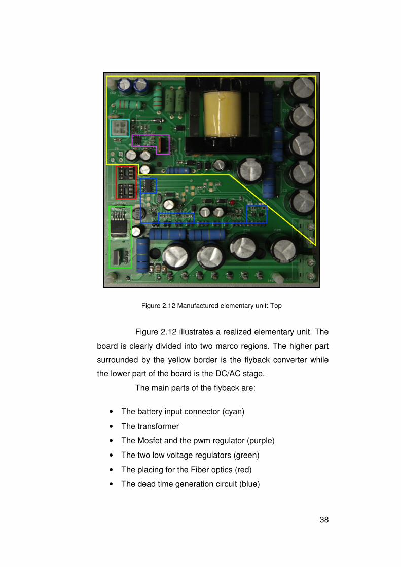
Figure 2.12 Manufactured elementary unit: Top
Figure 2.12 illustrates a realized elementary unit. The
board is clearly divided into two marco regions. The higher part
surrounded by the yellow border is the flyback converter while
the lower part of the board is the DC/AC stage.
The main parts of the flyback are:
• The battery input connector (cyan)
• The transformer
• The Mosfet and the pwm regulator (purple)
• The two low voltage regulators (green)
• The placing for the Fiber optics (red)
• The dead time generation circuit (blue)

Fig. 2.13
integrated inverter module is housed.
The elementary units have been stacked in piles. The
connections between each board has been done with the
common cables and with a series connected fuse.
Figure
Fig. 2.13 shows the lower view of the PCB where the
ated inverter module is housed.
The elementary units have been stacked in piles. The
connections between each board has been done with the
common cables and with a series connected fuse.
Figure 2.13 Manufactured elementary unit: Bottom
Figure 2.14 Stack of 8 elementary units
39
shows the lower view of the PCB where the
The elementary units have been stacked in piles. The
connections between each board has been done with the use of

All the boards have been split into 3 stacks of 8
PCBs. This was possible
and it was done for using it for three phase applications too. 24
switches had to be installed in order to activate each battery and
guarantee isolation. The batteries are also attached to external
plugs that are used
Finally as it can be seen the control unit is placed on
on top of the three pvc cases. 48 fiber optics travel from the
control board to all elementary units.
Figure 2.15 Complete system
All the boards have been split into 3 stacks of 8
PCBs. This was possible due to the modularity of the inverter
and it was done for using it for three phase applications too. 24
switches had to be installed in order to activate each battery and
guarantee isolation. The batteries are also attached to external
plugs that are used when recharging the inverter.
Finally as it can be seen the control unit is placed on
on top of the three pvc cases. 48 fiber optics travel from the
control board to all elementary units.
40
All the boards have been split into 3 stacks of 8
due to the modularity of the inverter
and it was done for using it for three phase applications too. 24
switches had to be installed in order to activate each battery and
guarantee isolation. The batteries are also attached to external
Finally as it can be seen the control unit is placed on
on top of the three pvc cases. 48 fiber optics travel from the

41
Chapter 3
SYSTEM IMPLEMENTATION: SOFTWARE AND
CONTROL
3.1 Control Method
The multilevel inverter is composed of 24 PCBs. Two
control signals are required on each board thus a total of 48
signals have to be generated and transferred to the inverter.
All typical control methods for multilevel converters
are based on modulation techniques. A very popular method
mainly used in industrial applications is the carrier-based
sinusoidal PWM that uses phase-shifting to reduce harmonics in
the load voltage. Another alternative is the Space Vector
Modulation strategy as well as the Space Vector PWM.
Each modulation method has its own advantages
though all of them share a common drawback which is that as
the number of levels increases the complexity of the control
implementation through digital means increases dramatically.
With respect to that consideration, a 49-level inverter poses a
big challenge.
In order turn the large number of levels from a
disadvantage point to an advantage a totally different approach
was chosen. The proposed technique is based on a
microcontroller unit that generates all 48 signals for the
multilevel. Each signal directly sets the state of the elementary
unit in accordance with the other units. Through the use of
appropriately set delays the switching instants for each IGBT is

controlled. Modulation is not neede
levels provides a good resolution detail on the output voltage.
Let us assume the already
Fig. 3.1, then
waveform is composed of 4 separate elementary units that
provide a given and same to each other output voltage. The
control method works on the triggering instants t1, t2 , etc. and
on the duration of the a
For example voltage V1 has to be set to the positive output
voltage at t1 and this event should last until t8 while V4 should
trigger at t4 and remain high until
controlled. Modulation is not needed as the large number of
levels provides a good resolution detail on the output voltage.
Figure 3.1 Multilevel waveform
Let us assume the already showed 9-level waveform,
, then the control method can be easily explained. This
waveform is composed of 4 separate elementary units that
provide a given and same to each other output voltage. The
control method works on the triggering instants t1, t2 , etc. and
on the duration of the applied voltage on each elementary unit.
For example voltage V1 has to be set to the positive output
voltage at t1 and this event should last until t8 while V4 should
ger at t4 and remain high until t5.
42
d as the large number of
levels provides a good resolution detail on the output voltage.
level waveform,
the control method can be easily explained. This
waveform is composed of 4 separate elementary units that
provide a given and same to each other output voltage. The
control method works on the triggering instants t1, t2 , etc. and
pplied voltage on each elementary unit.
For example voltage V1 has to be set to the positive output
voltage at t1 and this event should last until t8 while V4 should

43
This example shows how the voltage resolution of the
output waveform for 9 levels is low but scaling this control
method to a 49-level inverter makes this solution much more
reasonable. The 28,8 kV peak to peak output is divided into 600
V steps, i.e. ~2% of the total voltage.
3.2 The control unit
The mentioned control method has been
implemented with the use of a microcontroller board. High
processing power is not a strict requirement for the control unit.
However the number of available digital I/O is very important
because 48 signals have to be generated. The ATmega1280 8-
bit microcontroller from ATMEL was chosen which provides 54
digital I/O. The Arduino open source platform was used to
program the MCU which physically resides on the Arduino
board.
Figure 3.2 Arduino MCU

44
Included with the Arduino is the integrated
development environment (IDE) that serves as a programming
and compiling tool for the MCU. The programming can be done
in C language or in Assembly. The control algorithm is based on
the setting of firing instants and delays. As such it is very
sensitive to timing variations that can be introduced by software
loops or interrupts during the sequential execution of the
program. In order to prevent unexpected behaviour during
runtime the program had to be written in Assembly language
avoiding loops and disabling interrupts.
What follows is an example of the code that runs on
the MCU. In particular the first 4 steps of a triangular waveform
at 5 kHz are shown:
void setup()
DDRA = B11111111;
DDRB = B11111111;
void loop()
cli();
PORTA=B00000001;
PORTB=B00000000;
delayMicroseconds(4);
PORTA=B00000011;
PORTB=B00000000;
delayMicroseconds(4);
PORTA=B00000111;
PORTB=B00000000;
delayMicroseconds(4);
PORTA=B00001111;
PORTB=B00000000;
delayMicroseconds(4);

45
Like a normal C program the functions setup() and
loop() have to defined. In the setup the I/O registers A and B
are set as outputs by activating the all the bits. Because only 16
bits are set, i.e. two registers, it can be deduced that this code
refers to eight elementary units as two signals are needed to
drive each unit.
The instruction cli(); is necessary to disable
interrupts inside the loop. This is needed in order to have more
stable signals and avoid jitter effects that affect the output
signals of the MCU when interrupts are enabled.
The instruction PORTA=B00000001; sets the state of the
respective signals on register A. As it can be seen be the code
in order to generate a triangular wave the outputs have to be
progressively activated. Note that not only active signals have to
be set but also the 0s have to be reset each time in order to
avoid mistakes that have been noticed during runtime.
Finally the delayMicroseconds(4); sets the delay
between each voltage step in the multilevel staircase. The
minimum delay that can be set is 1 us.
As said low level language has been used in order to
avoid unnecessary delays due to high level commands’
execution during runtime. For example it has been measured
that the typical delay introduced by PORTA=BXXXXXXXX; instruction
is about 65ns while the respective high level command
introduces a delay of more than 400ns.

3.3 Simulations
A simulation of the complete multilevel inverter has
been developed in order to evaluate the expected behavio
when the system is connected to a load. A plasma actuator can
be roughly s
resistor of 1k
The simulation was develo
depicts the overview of the the model.
have been divided into three blocks that compr
just like the real implementation.
The output voltage is controlled by an input reference
signal. Arbitrary waveforms can be generated. In this example a
triangular waveform at 10 kHz was used. The value of the
reference signal ranges between
threshold value is ass
Simulations
A simulation of the complete multilevel inverter has
been developed in order to evaluate the expected behavio
when the system is connected to a load. A plasma actuator can
be roughly simulated as a series RC circuit. In particular a
resistor of 1kΩ and a capacitor of 10pF were set as the load.
The simulation was developed in Matlab – Simulink. Fig 3.3
depicts the overview of the the model. The elementary units
have been divided into three blocks that comprise of eight units,
just like the real implementation.
Figure 3.3 Simulink model of the total system
The output voltage is controlled by an input reference
signal. Arbitrary waveforms can be generated. In this example a
triangular waveform at 10 kHz was used. The value of the
reference signal ranges between -24 to 24. To each unit a
threshold value is assigned ranging from 0.5 to 23.5 with steps
46
A simulation of the complete multilevel inverter has
been developed in order to evaluate the expected behaviour
when the system is connected to a load. A plasma actuator can
In particular a
and a capacitor of 10pF were set as the load.
Simulink. Fig 3.3
The elementary units
ise of eight units,
The output voltage is controlled by an input reference
signal. Arbitrary waveforms can be generated. In this example a
triangular waveform at 10 kHz was used. The value of the
24 to 24. To each unit a
igned ranging from 0.5 to 23.5 with steps

of 1. For example the first unit (top left corner) the threshold
value is set to 0.5. The second unit takes a value of 1.5 and by
applying the same principle to all units the last one receives a
threshold value of
period of the triangular wave with the respective triggering
instants.
The elementary unit block is composed of two parts.
The first one is called “Driver”
comparing the reference signal value with the given threshold
value.
A deta
order to take into account the negative part of the reference
signal, i.e. the output waveform, the comparison is done both
with a positive value of the threshold
value Vth-. The converter block is just used to trans
numerical values to signals
of 1. For example the first unit (top left corner) the threshold
value is set to 0.5. The second unit takes a value of 1.5 and by
applying the same principle to all units the last one receives a
threshold value of 23.5. Fig. 3.4 shows the first positive quarter
period of the triangular wave with the respective triggering
Figure 3.4 Waveform formation
The elementary unit block is composed of two parts.
The first one is called “Driver”, Fig. 3.5, and it is responsible of
comparing the reference signal value with the given threshold
A detailed view of the driver, Fig. 3.6, shows that in
order to take into account the negative part of the reference
signal, i.e. the output waveform, the comparison is done both
with a positive value of the threshold Vth+ and with a negative
. The converter block is just used to trans
numerical values to signals Vmq1 and Vmq3.
47
of 1. For example the first unit (top left corner) the threshold
value is set to 0.5. The second unit takes a value of 1.5 and by
applying the same principle to all units the last one receives a
shows the first positive quarter
period of the triangular wave with the respective triggering
The elementary unit block is composed of two parts.
is responsible of
comparing the reference signal value with the given threshold
shows that in
order to take into account the negative part of the reference
signal, i.e. the output waveform, the comparison is done both
and with a negative
. The converter block is just used to transform

Vmq1
to the second block that composes the elementary unit which is
the “H-bridge” shown in Fig. 3.7
possible states:
1.
2.
3.
Vmq1 and Vmq3 are the control signals that are fed
to the second block that composes the elementary unit which is
bridge” shown in Fig. 3.7. The H-bridge can have three
possible states:
Figure 3.5 Elementary unit model
Figure 3.6 Driver model
Q1,Q4 closed and Q3,Q2 open when the reference
signal is above the threshold and the output
voltage is positive (600 V).
Q3,Q2 closed and Q1,Q4 open when the reference
signal is below the threshold and th
voltage is negative (-600 V).
Q2,Q4 closed and Q1,Q3 open when the reference
signal is between the positive and the negative
values of the threshold and the output voltage is 0.
Basically the unit is by-passed.
48
are the control signals that are fed
to the second block that composes the elementary unit which is
bridge can have three
Q1,Q4 closed and Q3,Q2 open when the reference
signal is above the threshold and the output
Q3,Q2 closed and Q1,Q4 open when the reference
signal is below the threshold and the output
Q3 open when the reference
signal is between the positive and the negative
values of the threshold and the output voltage is 0.

The final 49 level outpu
3.8.
As it can be seen the voltage goes from
14,4 kV and all elementary units are used. The reference
waveform is perfectly replicated on the output.
Fig. 3.9
nature of the load the current has a totally different waveform
than that of the voltage. In fact it is a series of spikes. Between
each spike the current goes to zero. As it will later be shown this
is a very real
current spikes happen in correspondence to the voltage steps,
either positive or negative, the polarity obviously follows that of
the voltage. This fact shows that elementary units conduct
current in a discont
after switching.
The final 49 level output voltage is depicted in Fig.
Figure 3.7 H-bridge model
As it can be seen the voltage goes from -
14,4 kV and all elementary units are used. The reference
waveform is perfectly replicated on the output.
Fig. 3.9 shows the current. Due to the capacitive
nature of the load the current has a totally different waveform
than that of the voltage. In fact it is a series of spikes. Between
each spike the current goes to zero. As it will later be shown this
is a very realistic behaviour of a plasma actuator load.
current spikes happen in correspondence to the voltage steps,
either positive or negative, the polarity obviously follows that of
the voltage. This fact shows that elementary units conduct
current in a discontinuous way and only for a short period of time
after switching.
49
depicted in Fig.
-14,4 kV to
14,4 kV and all elementary units are used. The reference
shows the current. Due to the capacitive
nature of the load the current has a totally different waveform
than that of the voltage. In fact it is a series of spikes. Between
each spike the current goes to zero. As it will later be shown this
istic behaviour of a plasma actuator load. The
current spikes happen in correspondence to the voltage steps,
either positive or negative, the polarity obviously follows that of
the voltage. This fact shows that elementary units conduct
inuous way and only for a short period of time

Figure 3.8 Simulated output voltage waveform
50

Figure 3.9 Simulated output current
51

3.4 Input power balancing
It should be clear by now that if the implemented
control method was a strict copy of the previously showed
simulation an unbalance on the use of the modules would
happen. It is evident that if the thresholds of each unit are
statically set
shows the level voltage of
unit V24 which correspond respectively to the lowest threshold
value and to the highest. Only a few cycles are needed in order
to show that the unit that has th
for a longer period of time that V24 which has the higher
threshold and therefore activates only when the reference signal
peaks at its limits.
Evidently the unit with the lower threshold conducts
current while active for much longer time than the one with the
highest threshold. Thus the unit that corresponds to V1 provides
more power to the system than the unit that has V24 voltage.
For a multilevel inverter that it is based on batteries this means
Input power balancing
It should be clear by now that if the implemented
control method was a strict copy of the previously showed
simulation an unbalance on the use of the modules would
happen. It is evident that if the thresholds of each unit are
set some units “work” more than others. Fig 3.10
shows the level voltage of the first unit V1 and that of the last
unit V24 which correspond respectively to the lowest threshold
value and to the highest. Only a few cycles are needed in order
to show that the unit that has the lowest threshold, V1, is active
for a longer period of time that V24 which has the higher
threshold and therefore activates only when the reference signal
peaks at its limits.
Figure 3.10 Detailed view of V1 and V24
Evidently the unit with the lower threshold conducts
current while active for much longer time than the one with the
highest threshold. Thus the unit that corresponds to V1 provides
more power to the system than the unit that has V24 voltage.
vel inverter that it is based on batteries this means
52
It should be clear by now that if the implemented
control method was a strict copy of the previously showed
simulation an unbalance on the use of the modules would
happen. It is evident that if the thresholds of each unit are
k” more than others. Fig 3.10
first unit V1 and that of the last
unit V24 which correspond respectively to the lowest threshold
value and to the highest. Only a few cycles are needed in order
e lowest threshold, V1, is active
for a longer period of time that V24 which has the higher
threshold and therefore activates only when the reference signal
Evidently the unit with the lower threshold conducts
current while active for much longer time than the one with the
highest threshold. Thus the unit that corresponds to V1 provides
more power to the system than the unit that has V24 voltage.
vel inverter that it is based on batteries this means

53
that the battery connected to the first unit will discharge faster
than the one connected to the second unit.
This can be a problem for two reasons. First of all if
the batteries are discharged in different manner the use of the
multilevel before a recharge cycle is bonded to the battery life of
the lowest threshold unit. Thus the system could stop working
properly only due to a couple of discharged batteries while the
rest could still function. This leads to the second problem which
has to do with the expected lifetime of the batteries. The optimal
way of charging requires the batteries to be at the same level of
charge. In this condition this would be problematic.
In order to solve this issue a couple of more
advanced control methods were simulated, with one of them
actually being implemented on the real system. These
algorithms are an attempt to render the discharge of the
batteries homogenous.
3.5 Cycling Levels
The first control method is also the one that has been
implemented on the real system. It is an open loop control
method. The idea is to vary the thresholds of the units in order to
have them periodically cycle. This way the power supplies
(batteries) would be active for the same amount of time of a
certain period.
In order to implement this system an “Embedded
Matlab Function” had to be inserted into the simulink model. This
block executes a script when activated. The activation is
governed by the clock block. At the start of the simulation time a
vector of thresholds is input to the units. The values of the vector
correspond to the values seen in the previous paragraph. The

difference is that after a pre
rotated so that for example the threshold value of the first u
becomes the one of the second. Obviously this event happens
simultaneously for all units.
Fig. 3.12
elementary unit. As it is evident after each period of the
reference signal the threshold moves from a lower unit to a
higher. After 24 periods a full cycle of the thresholds is
completed and the algorithm is re
units is kept just for reference and is no more assigned to a
particular threshold value.
This control method balances the discharges of the
power supplies very efficiently especially for symmetric
waveforms like the triangle.
power balancing might be needed in order to react to power
mismatch in a more immediate way rather than periodically. For
this reason another balancing method has been developed.
difference is that after a pre-determined period the vectors are
rotated so that for example the threshold value of the first u
becomes the one of the second. Obviously this event happens
simultaneously for all units.
Figure 3.11 Cycling levels model
Fig. 3.12 shows the output voltage of each individual
elementary unit. As it is evident after each period of the
reference signal the threshold moves from a lower unit to a
higher. After 24 periods a full cycle of the thresholds is
completed and the algorithm is repeated. The numbering of the
units is kept just for reference and is no more assigned to a
particular threshold value.
This control method balances the discharges of the
power supplies very efficiently especially for symmetric
waveforms like the triangle. Sometimes though a more dynamic
power balancing might be needed in order to react to power
mismatch in a more immediate way rather than periodically. For
this reason another balancing method has been developed.
54
determined period the vectors are
rotated so that for example the threshold value of the first unit
becomes the one of the second. Obviously this event happens
shows the output voltage of each individual
elementary unit. As it is evident after each period of the
reference signal the threshold moves from a lower unit to a
higher. After 24 periods a full cycle of the thresholds is
peated. The numbering of the
units is kept just for reference and is no more assigned to a
This control method balances the discharges of the
power supplies very efficiently especially for symmetric
Sometimes though a more dynamic
power balancing might be needed in order to react to power
mismatch in a more immediate way rather than periodically. For
this reason another balancing method has been developed.

Figure 3.12 Cycling levels waveforms
55

3.6 Dynamic Balancing
A more complex balancing scheme has been
implemented for cases where cycling the levels is not enough
and a more immediate action is required. As seen the previous
algorithm is a static method. In order to have a faster and more
accurate algorithm a feedback loop had to be introduced. In
particular the dynamic balancing method that is presented in this
section requires a voltage and current measurement of each
elementary level.
These measurements are
power produced by eac
Dynamic Balancing
A more complex balancing scheme has been
implemented for cases where cycling the levels is not enough
and a more immediate action is required. As seen the previous
algorithm is a static method. In order to have a faster and more
algorithm a feedback loop had to be introduced. In
particular the dynamic balancing method that is presented in this
section requires a voltage and current measurement of each
elementary level.
Figure 3.13 Dynamic balancing model
These measurements are multiplied and the instant
power produced by each unit is calculated. In Fig. 3.13
56
A more complex balancing scheme has been
implemented for cases where cycling the levels is not enough
and a more immediate action is required. As seen the previous
algorithm is a static method. In order to have a faster and more
algorithm a feedback loop had to be introduced. In
particular the dynamic balancing method that is presented in this
section requires a voltage and current measurement of each
multiplied and the instant
h unit is calculated. In Fig. 3.13 the three

57
vectors Pwr1, Pwr2 and Pwr3 carry 8 element vectors that
contain the calculated powers for each unit. These
measurements are then fed into a windowed integrator
Figure 3.14 Windowed integrator
The integrator computes the integral value of the
input power during a given period of time. This period is set to
50us which half of the period of the reference signal (10kHz).
This calculation produces the provided energy by each unit.
The window integrator is composed of two integrator
blocks the second one of which receives a delayed sample of
the power. Thus by computing the difference between the two
integrator blocks the energy in a given time frame is calculated.
A reset signal is necessary in order to avoid
saturation. When this signal is triggered the output of the first
integrator is set to the difference value between the two
integrators while the second one is set to zero. This way the
output of the windowed integrator is consistent.
A Sample and Hold block receives the 24 calculated
energy values and samples them with a period of 50 us in order
to provide constant values to the Embedded Matlab Function. In
this case too, on the input of the block there is the vect vector
with the old threshold values while on the output the new
threshold values are generated though the new_vect every 50
us.

58
The implemented algorithm orders the new threshold
values in function of the calculated energy values. The unit that
has provided the most power during the previous sample period
receives the highest threshold while the one that has provided
the least energy receives the lowest threshold, thus it will be the
one that will be active for the most time during the next cycle.
What follows is the code executed when the Embedded Matlab
Function is activated:
function new_vect = fcn(vect, energy)
new_vect=vect;
for i=0:1:(length(vect)-1)
[max, posmax]=max(energy);
new_vect(posmax)=23.5-i;
energy(posmax)=0;
end;
end
A 24 iterations cycle is executed during which the
maximum value of the energy vector is found as well as its
position with the use of the m(energy) function. The highest
threshold value is then assigned to the corresponding unit and
the previously calculated maximum value of the energy is set to
zero. This is done in order to find the second highest energy
value then third etc.

59
Chapter 4
EXPERIMENTAL RESULTS
4.1 17 levels vs sinusoidal
The multilevel has been tested in the lab in a gradual
way. The first experiments involved just few elementary units in
order to be sure of the correct functioning of the multilevel. The
first major step was when a stack of 8 units was put together.
Fig. 4.1 shows a triangular waveform. The peak to
peak voltage is 9.6 kV and the frequency is 8 kHz. Note that in
this experiment the zero step voltage was omitted. The plasma
actuator has a length of 4 cm and the dielectric is 2 mm deep
made of kapton.
The lower part of the figure shows the respective
current measured on the low voltage electrode. As expected an
impulsive type of current is seen. Peaks reach values of around
0.5 and can be detected only when there is a voltage step,
either positive or negative.
Fig. 4.2 shows the voltage and current measured on
the load when a sinusoidal power supply is applied. The peak to
peak voltage as well as the frequency are the same like in the
multilevel case.
A clear advantage of the multilevel current waveform
is the lack of the capacitive component which generates that low
frequency variation that can be seen on the sinusoidal power
supply current graph. Plasma is only produced during
discharges so having a low frequency component in the current

does not provide any effect. As a matter of fact it
factor because it is a cause of inefficiency.
Another advantage of the multilevel inverter against
the sinusoidal is the measured power delivered to the plasma
actuator. The multilevel is able to provide 3.8 W vs the
sinusoidal’s 1.9 W.
These first results showed that the
more power
efficient.
does not provide any effect. As a matter of fact it is a negative
factor because it is a cause of inefficiency.
Another advantage of the multilevel inverter against
the sinusoidal is the measured power delivered to the plasma
or. The multilevel is able to provide 3.8 W vs the
sinusoidal’s 1.9 W.
These first results showed that the multilevel delivers
to the plasma actuator and is generally more
Figure 4.1 Triangular waveform
Figure 4.2 Sine waveform
60
is a negative
Another advantage of the multilevel inverter against
the sinusoidal is the measured power delivered to the plasma
or. The multilevel is able to provide 3.8 W vs the
multilevel delivers
a actuator and is generally more

61
4.2 Full voltage tests
This section illustrates a series of experimental
results that have been done with different types of waveform.
These tests were used to prove the functionality of the multilevel
generator at its final configuration, generating 49 levels of output
voltage. These tests were conducted in collaboration with Alenia
Aermacchi both at the DEI labs as well as at the AAM labs.
The dielectric material that has been used was a Plexi
84. It is a special type of Polymethyl methacrylate. The use of
this material is mandatory for avionic applications when a
transparent thermoplastic surface has to be used because of the
high robustness to corrosion and the long expected lifetime it
can provide as opposed to other plastic materials. The thickness
of the dielectric was 4 mm.
Both the high voltage and low voltage electrode were
made of copper which comes in parts of tape that are stitched
on the dielectric surface. The high voltage electrode was
connected to the high voltage output connector of the multilevel
while the low voltage electrode was connected to the low voltage
output and to the ground.
The measurements were done using a Yokogawa
Dl6054 digital oscilloscope. Voltage was measured with the use
of a 20 kV voltage probe while the current sensing was done
using a hall effect sensor probe. Due to the impulsive nature of
the current its measurement has been particularly challenging to
achieve. Other types of sensors were tested, like an
amperometric transformer or even series connected resistor, but
the Hall effect sensor probe was the one that gave the most
reliable and realistic results.

62
The main purpose of the following tests was to
compare the results with those given by a resonant converter. In
particular the load matching of the resonant converter could
happen only at a certain frequency of about 6.2 kHz. It was of
particular interest to try to supply the plasma actuator at lower
frequencies. That is why most of the results that will be shown
were generated at lower frequencies with respect to the
multilevel’s maximum frequency of 20 kHz
4.2.1 Square waveform
Figure 4.3 shows the voltage and current
measurements for a square waveform. The full 28.8 kV peak to
peak voltage was applied to the actuator at 5 kHz frequency.
The size of the electrodes was 40 cm in length and 1 cm in width
The shape of this type of waveform can be split into
two regions. The first on is where all 24 H-bridges switch
simultaneously and the voltage peak is generated. During a
single period of the wave form this event happens twice, once
from the lower negative point to the top positive point and once
from the top positive point to the lower negative point.
The second region of the waveform is a long plateau
were the voltage is kept a constant level. In this part of the
waveform the state of all H-bridges is constant, no switching
happens. In reality it can be seen that the plateau is not perfectly
horizontal as there is a small slope both on the positive side as
well as on the negative. This is due to high capacitive couplings
that happen when the multilevel is functioning. This capacitive
polarization generates a small overshoot of the voltage when
more than one H-bridges are simultaneously switched to the

63
same direction. In this case, due to the fact that all H-bridges
switch simultaneously this effect is very evident.
During this overshoot the voltage reaches a maximum
value of about ±15.7 kV. For the positive side of the voltage it
can be seen that after this initial over-voltage there is a negative
slope that leads to the actual 14.4 kV voltage of the multilevel.
Vice versa for the negative voltage.
This phenomenon is not really a negative effect for
the purpose of these experiments. As previously said plasma is
formed when a discharge happens. Thus what is contributing to
plasma generation are the current spikes that are generated. In
fact the regions where the current is zero are have no real effect
on the plasma. Therefore, a voltage overshoot that leads to a
slightly higher current spike is actually a positive consequence.
Obviously, that is not to say that this effect should not be
controlled but in a restrained way and inside some margins it
was intentionally accepted when testing the multilevel.
The measured current spike when peak-to-peak
voltage switches happen is roughly 1.5 A both positive and
negative. It should be noted that in the region when the voltage
has a plateau the current is never actually zero. This happens
because small discharges happen even when constant voltage
is applied. This effect makes the calculation of the useful power
provided to the plasma actuator quite difficult.
In order to get a rough estimate of the power
delivered to load an average had to be calculated over a series
of periods of the voltage and current measures. The square
waveform’s power resulted in 67 W.

Figure 4.3 Square waveform
64

65
Figures 4.4 present a detailed view of both voltage
and current waveforms during the negative and positive
transients. In both cases the transient time for a peak-to-peak
28.8 kV switch is about 500 ns. This corresponds to a voltage
rate of 60 kV/us. These measures prove the how well the
multilevel performs in these situations. The voltage step is
almost symmetric on both variations. As noted before a small
ringing effect on the current is seen where it oscillates around
the zero value.
Figure 4.4 Detailed view of the voltage and the current

66
4.2.2 Triangular Waveform
Fig. 4.6 shows the voltage and current measurements
for a triangular waveform at full voltage and at 4.9 kHz. The
electrodes were 10 cm long. In this case the H-bridges have
been switched two at a time, thus 12 positive steps and 12
negative steps can be counted. Each voltage step measures
1200 V. As it can be noted even though the peak voltage is the
same as the square waveform the current peak is significantly
lower due to the shorter electrodes and to the type of waveform.
Maximum current is 0.15 A. In this case though the distribution
of the spikes is also different. Due to the fact that the total
voltage waveform is composed of many voltage steps the
number of spikes during a single period is much bigger. In the
end this results in more power delivered to the load as opposed
to higher but scarce current spikes.
Figure 4.6 Triangular waveform
Fig. 4.7 shows the simulated version of the triangular
waveform applied to a series R-C load. A plasma actuator can
be quite difficult to model as it as the value of the impedance
can dynamically change during the discharges. Therefore a

static load was chosen to be used in order to have a rough
estimate of how the multilevel would behave.
The shape
has been measured though the simulated one generates
constant value spikes. This is not happening in the real syst
where the spikes have different values. This can be explained by
the fact that as said the actual impedance of the actuator is
dynamically varying during the experiments and also because
capacitive couplings have not been taken into account in the
simulation.
4.2.3 Sawtooth
Fig. 4.8
a negative slope sawtooth waveform
In this case all H
providing voltage steps of 600 V during the slope section. This
type of waveform can be thought of as a mix between the
triangular and the square waveform due to the fact that there is
static load was chosen to be used in order to have a rough
imate of how the multilevel would behave.
Figure 4.7 Simulated triangular waveform
The shape of the current is very close to the one that
has been measured though the simulated one generates
constant value spikes. This is not happening in the real syst
where the spikes have different values. This can be explained by
the fact that as said the actual impedance of the actuator is
dynamically varying during the experiments and also because
capacitive couplings have not been taken into account in the
Sawtooth
Fig. 4.8 shows the measured voltage and current for
a negative slope sawtooth waveform with 10 cm long electrodes.
In this case all H-bridges have been used separately thus
providing voltage steps of 600 V during the slope section. This
e of waveform can be thought of as a mix between the
triangular and the square waveform due to the fact that there is
67
static load was chosen to be used in order to have a rough
of the current is very close to the one that
has been measured though the simulated one generates
constant value spikes. This is not happening in the real system
where the spikes have different values. This can be explained by
the fact that as said the actual impedance of the actuator is
dynamically varying during the experiments and also because
capacitive couplings have not been taken into account in the
shows the measured voltage and current for
0 cm long electrodes.
bridges have been used separately thus
providing voltage steps of 600 V during the slope section. This
e of waveform can be thought of as a mix between the
triangular and the square waveform due to the fact that there is

68
a large current spike followed by lower though frequent spikes.
The top current value has been measured to be 0.22.
Figure 4.8 Sawtooth waveform
Fig. 4.9 Shows the simulated version of this
waveform. The difference with the real one is more evident in
this case. The current peaks where there is a high voltage
switch though the rest of the spikes are much lower. As said the
presented simulations are needed to get a rough estimate of the
behaviour of the current not a perfect match.
Figure 4.9 Simulated sawtooth waveform
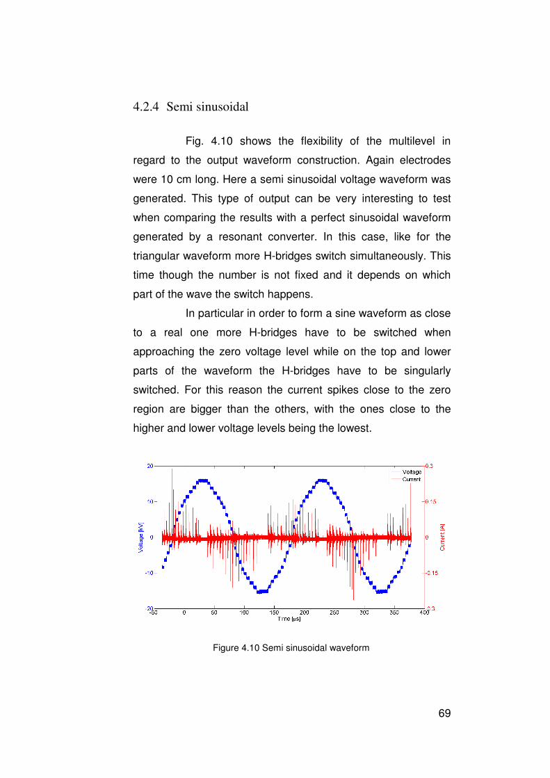
69
4.2.4 Semi sinusoidal
Fig. 4.10 shows the flexibility of the multilevel in
regard to the output waveform construction. Again electrodes
were 10 cm long. Here a semi sinusoidal voltage waveform was
generated. This type of output can be very interesting to test
when comparing the results with a perfect sinusoidal waveform
generated by a resonant converter. In this case, like for the
triangular waveform more H-bridges switch simultaneously. This
time though the number is not fixed and it depends on which
part of the wave the switch happens.
In particular in order to form a sine waveform as close
to a real one more H-bridges have to be switched when
approaching the zero voltage level while on the top and lower
parts of the waveform the H-bridges have to be singularly
switched. For this reason the current spikes close to the zero
region are bigger than the others, with the ones close to the
higher and lower voltage levels being the lowest.
Figure 4.10 Semi sinusoidal waveform

70
In Fig. 4.11 a simulated sine voltage waveform is
shown. Note that in this case a perfect sine wave is depicted.
For this simulation the same comments as for what said for the
triangular waveform simulation stand true.
Figure 4.11 Sine waveform
4.2.5 Positive triangle
Fig. 4.12 is another display of how the multilevel
within its resolution limits can generate arbitrary waveform. In
particular an only positive triangular waveform at 10 kHz is
shown. With 10 cm long electrodes the voltage peak value is still
14.4 kV while the H-bridges are switched 2 at the time. The
measured current is significantly lower than the other cases and
this type of waveform is not particularly efficient on a plasma
actuator load.
Though, generating a voltage waveform with non zero
average value can be a very interesting case study for how
charged particles deposited on the borders of the dielectric react
to an only positive alternating voltage. Obviously, the same type
of waveform can be generated with negative voltage values too.

4.3 Velocity measures
This section provides some measured results with
regard to the actual fluid dynamic force that has been generated
with the plasma actuator when a multilevel AC voltage was
applied. The measure of the fluid (air) speed has been done with
the use of a Pitot
The used dielectric material was again a Plexi83 with
a 4 cm thickness. The electrodes were 40 cm long and 1 cm
wide. The measures have been done
distances from the end
away from it. In particular 12 mm and 20 mm measures were
executed. This was useful in order to better understand
the intensity of the force but also the length. Different types of
waveform were used.
Fig. 4.13 shows the measures
reference here is the black curve which has been generated by
a resonant converter. For each tested waveform 10 samples
Figure 4.12 Positive triangular waveform
Velocity measures
This section provides some measured results with
regard to the actual fluid dynamic force that has been generated
with the plasma actuator when a multilevel AC voltage was
applied. The measure of the fluid (air) speed has been done with
the use of a Pitot tube sensor.
The used dielectric material was again a Plexi83 with
cm thickness. The electrodes were 40 cm long and 1 cm
wide. The measures have been done starting from two
distances from the end of the generated plasma and moving
. In particular 12 mm and 20 mm measures were
executed. This was useful in order to better understand
the intensity of the force but also the length. Different types of
waveform were used.
Fig. 4.13 shows the measures starting at 12 mm. The
ence here is the black curve which has been generated by
a resonant converter. For each tested waveform 10 samples
71
This section provides some measured results with
regard to the actual fluid dynamic force that has been generated
with the plasma actuator when a multilevel AC voltage was
applied. The measure of the fluid (air) speed has been done with
The used dielectric material was again a Plexi83 with
cm thickness. The electrodes were 40 cm long and 1 cm
starting from two different
and moving
. In particular 12 mm and 20 mm measures were
executed. This was useful in order to better understand not only
the intensity of the force but also the length. Different types of
at 12 mm. The
ence here is the black curve which has been generated by
a resonant converter. For each tested waveform 10 samples

were measured and then averaged in order to have a more
stable result.
As it can be seen most of
outperformed by the resonant converter
sinusoidal (yellow)
absolute peak in fluid dynamic force though was measured with
the sawtooth waveform (green) which
maximum value close to the plasma formation but the
decreases very rapidly.
Fig. 4.14 shows the result with the pitot sensor
starting at 20 mm. Apart from the positive and negative
triangular waveforms
mentioned are not particularly efficient on plasma actuator loads
were measured and then averaged in order to have a more
Figure 4.13 Velocity starting at 12 mm
As it can be seen most of the waveforms are
outperformed by the resonant converter (black) with the semi
(yellow) waveform almost matching this result. The
absolute peak in fluid dynamic force though was measured with
the sawtooth waveform (green) which has the absolute
maximum value close to the plasma formation but the
very rapidly.
Fig. 4.14 shows the result with the pitot sensor
starting at 20 mm. Apart from the positive and negative
triangular waveforms (purple and dotted) that as already
mentioned are not particularly efficient on plasma actuator loads
72
were measured and then averaged in order to have a more
the waveforms are
with the semi
waveform almost matching this result. The
absolute peak in fluid dynamic force though was measured with
has the absolute
maximum value close to the plasma formation but then
Fig. 4.14 shows the result with the pitot sensor
starting at 20 mm. Apart from the positive and negative
that as already
mentioned are not particularly efficient on plasma actuator loads

The remaining waveform provide closer results. The sawtooth is
again the one that provides the top velocity.
The remaining waveform provide closer results. The sawtooth is
again the one that provides the top velocity.
Figure 4.14 Velocity starting at 20 mm
73
The remaining waveform provide closer results. The sawtooth is

74
Chapter 5
CONCLUSIONS
The realization of a high-voltage high-frequency
arbitrary voltage generator has been the subject of this
dissertation. All design steps have been shown as well as the
final implementation. The experimental results show how the
multilevel converter is able to actually generate high voltage high
frequency arbitrary waveforms independently of the type of
plasma actuator.
The presented system has been successfully
accepted by Alenia Aermacchi as the reference model for the
design of a multilevel converter which, as only difference, will be
powered by AC voltage instead of batteries. As shown isolation
issues can rise when using a transformer to power a cascaded
inverter. Thus future investigations on this type of power supply
are needed.
Another future development would be to fine tune the
simulink model at IGBT level in order to have even more realistic
results and not just a qualitative behaviour of the current. This
would also permit to correctly model the load.
Finally, fluid dynamic effects of plasma actuators are
still at primary research level. For this reason experimental
results on velocity should by no means be considered
completed. The implementation of the presented cascaded
multilevel inverter opens up new possibilities for the study of the
plasma actuators and provides an important tool for the
continuation of this research.

75
References
[1] C. Tendero, C. Tixier, P. Tristant, J. Desmaison, P.
Leprince, “Atmospheric pressure plasmas: A review,”
Spectrochimica Acta Part B: Atomic Spectroscopy, vol. 61, No.
1, pp. 2-30, Jan. 2006.
[2] L. Bárdos, H. Baránková, “Cold atmospheric
plasma: Sources, processes, and applications,” Thin Solid Films,
vol. 518, No. 23, pp. 6705-6713, Sept. 2010.
[3] A. Fridman, A. Chirokov and A. Gutsol. “Non-
thermal atmospheric pressure discharges” .J. Phys D: Appl
Phys, 38: R1-R24, 2005.
[4] U. Kogelschatz. “Atmospheric-pressure plasma
technology”. Plasma Phys. Control. Fusion, vol 46, issue 12B,
B63-B75, 2004, DOI: 10.1088/0741-3335/46/12B/006.
[5] J.Y. Jeong, S. E. Babayan, V. J. Tu, J. Park, I.
Henins, R. F. Hicks and G. S. Selwyn.. “Etching materials with
an atmospheric pressure plasmas jet”. Plasma Sources Sci
Technol, 7: 282-285, 1998.
[6] N. Yaman, E. Özdoǧan, and N. Seventekin,
“Atmospheric plasma treatment of polypropylene fabric for
improved dyeability with insoluble textile dyestuff”, Fibers and
Polymers, February 2011, Vol. 12, No. 1, pp. 35-41.
[7] S. Lerouge, M.R. Wertheimer and L’H. Yahia
“Plasma Sterilization: A Review of Parameters, Mechanisms,
and Limitations” Plasmas and Polymers, Vol. 6, No. 3, Sept.
2001.
[8] M. Been Chang, C. Chun-Cheng, “Destruction and
removal of toluene and MEK from gas streams with silent

76
discharge plasmas ” American Institute of Chemical Engineers.
AIChE Journal; May 1997; 43, 5; pg. 1325
[9] G.J. Pietscha and V.I. Gibalovb “Dielectric barrier
discharges and ozone synthesis“ Pure&Appl. Chem.,Vol.70, No.
6, pp. 1169-1174,1998
[10] S. Min, G.A. Evrendilek, H.Q. Zhang, “Pulsed
Electric Fields: Processing System, Microbial and Enzyme
Inhibition, and Shelf Life Extension of Foods,” IEEE Trans. on
Plasma Science, vol. 35, No. 1, pp. 59-73, Feb. 2007.
[11] A. H. El-Hag, S. H. Jayaram, M.W. Griffiths,
“Inactivation of Naturally Grown Microorganisms in Orange Juice
Using Pulsed Electric Fields,” Plasma Science, IEEE
Transac¬tions on, vol. 34, iss. 4, pt. 2, pp. 1412-1415, Aug.
2006
[12] M. Laroussi, “Low Temperature Plasma-Based
Sterilization: Overview and State-of-the-Art,” Plasma Processes
and Polymers, vol. 2, iss. 5, pp. 391-400, Jun. 2005.
[13] G. Friedman, A. Gutsol, A.B. Shekhter, V.N.
Vasilets, A. Fridman, “Applied Plasma Medicine”, Plasma
Processes and Polymers, Vol. 5, Issue 6, Article first published
online: 16 Apr. 2008.
[14] T.C. Corke, C. Lon Enloe, S. P. Wilkinson,
“Dielectric Barrier Discharge Plasma Actuators for Flow Control,”
Annual Review of Fluid Mechanics, vol. 42, pp. 505-529, 2010.
[15] N. Benard, E. Moreau, “Role of the electric
waveform supplying a dielectric barrier discharge plasma
actuator,” Applied Physics Letters, vol. 100, iss. 9, ref. 193503,
May 2012.
[16] A. Cristofolini, C.A. Borghi, and G. Neretti
“Charge distribution on the surface of a dielectric barrier

77
discharge actuator for the fluid-dynamic control”, J. of Appl.
Phys. 113, 143307 (2013), DOI: 10.1063/1.4799159.
[17] A. Cristofolini, G. Neretti, and C. A. Borghi,
“Effect of the charge surface distribution on the flow field
induced by a dielectric barrier discharge actuator” J. Appl. Phys.
114, 073303 (2013); doi: 10.1063/1.4817378.
[18] Song Guo, “An Investigation of Dielectric Barrier
Discharge Based Plasma Actuator Designs With Enhanced
Performance In Active Flow Control,” PhD dissertation,
University of Minnesota
[19] J. Rodriguez, S. Bernet, Bin Wu, J. O. Pontt,
“Multilevel Voltage-Source-Converter Topologies for Industrial
Medium-Voltage Drives,” IEEE Trans. on Industrial Electronics,
vol. 54, iss. 6, pp. 2930-2945, Dec. 2007
[20] J. Rodriguez, Jih-Sheng Lai, Fang Zheng Peng,
“Multilevel inverters: a survey of topologies, controls, and
applications,” IEEE Trans. on Industrial Electronics, vol. 49, iss.
4, pp. 724-738, Aug 2002
[21] Mitsubishi Electric, “Dual-In-Line Package
Intelligent Power Module,” PS22A74 datasheet, Jan. 2012.