Algorithm/Architecture Co-Design for Wireless ...vada.skku.ac.kr/ClassInfo/dsp/sdr/ningzhang.pdf1...
250
Algorithm/Architecture Co-Design for Wireless Communications Systems by Ning Zhang B.S. (California Institute of Technology) 1996 M.S. (University of California, Berkeley) 1998 A dissertation submitted in partial satisfaction of the requirements for the degree of Doctor of Philosophy in Engineering-Electrical Engineering and Computer Sciences in the GRADUATE DIVISION of the UNIVERSITY OF CALIFORNIA, BERKELEY Committee in charge: Professor Robert W. Brodersen, Chair Professor A. Richard Newton Professor Paul K. Wright Fall 2001
Transcript of Algorithm/Architecture Co-Design for Wireless ...vada.skku.ac.kr/ClassInfo/dsp/sdr/ningzhang.pdf1...

Algorithm/Architecture Co-Design for Wireless Communications Systems
by
Ning Zhang
B.S. (California Institute of Technology) 1996 M.S. (University of California, Berkeley) 1998
A dissertation submitted in partial satisfaction of the
requirements for the degree of
Doctor of Philosophy
in
Engineering-Electrical Engineering and Computer Sciences
in the
GRADUATE DIVISION
of the
UNIVERSITY OF CALIFORNIA, BERKELEY
Committee in charge:
Professor Robert W. Brodersen, Chair Professor A. Richard Newton
Professor Paul K. Wright
Fall 2001

Algorithm/Architecture Co-Design for Wireless Communications Systems
Copyright 2001
by
Ning Zhang


1
Abstract
Algorithm/Architecture Co-Design for Wireless Communications Systems
by
Ning Zhang
Doctor of Philosophy in Engineering-Electrical Engineering and Computer Sciences
University of California, Berkeley
Professor Robert W. Brodersen, Chair
Wireless connectivity is playing an increasingly significant role in communication
systems. Advanced communication algorithms have been developed to combat multi-
path and multi-user interference, as well as to achieve increased capacity and better
spectral efficiency. To meet the needs of performance with low energy consumption
requires not only the use of most advanced integrated circuit technology, but
architecture and circuit design techniques which have the highest possible energy and
area efficiencies. This requires the design rely on the integration of algorithm
development and architecture choice that exploits the full potential of theoretical
communications results and advanced CMOS technology. Unfortunately, the lack of
such a unified design methodology currently prevents the exploration of various
realizations over a broad range of algorithmic and architectural options.
These strategies were employed to study the algorithms and architectures for the
implementation of digital signal processing systems, which exploit the interactions
between the two to derive energy and cost efficient solutions of high-performance
wireless digital receivers. First, a front-end design methodology is developed to facilitate
algorithm/architecture exploration of dedicated hardware implementation. The
proposed methodology provides efficient and effective feedback between algorithm and

2
architecture design. High-level implementation estimation and evaluation is used to
assist systematic architecture explorations.
Second, multiple orders of magnitude improvement in both energy and area (cost)
efficiency can be obtained by using dedicated hardwired and highly parallel
architectures (achieving 1000 MOPS/mW and 1000 MOPS/mm2) compared to running
software on digital signal processors. These significant differences are studied and
analyzed to gain insight into an energy and area efficient design approach that best
exploits the underlying state-of-the-art CMOS technology. In addition, by combining the
system design, which identifies a constrained set of flexible parameters, and an
architectural implementation, which exploits the algorithm’s structure, it is
demonstrated in this thesis that efficiency and flexibility can be both achieved, which
otherwise would be a fundamental trade-off.
Third, the advantages of bringing together system and algorithm design, architecture
design, and implementation technology are demonstrated by example designs of
wireless communications systems at both block level and system level: multi-user
detection for CDMA system, multi-antenna signal processing, OFDM system, and multi-
carrier multi-antenna system. Design examples all show that optimized architecture
through the co-design offers 2-3 orders of magnitude higher computation density than
can be achieved by other common DSP solutions: software processors, FPGA’s or
reconfigurable data-paths, at the same time, providing 2 to 3 orders of magnitude
savings in energy consumption.
Robert W. Brodersen, Chair
i
Table of Contents
List of Figures iv List of Tables vi Acknowledgments vii
Chapter 1 Introduction 1 1.1 Motivation 1 1.2 Research goals 5 1.3 Thesis organization 7 Chapter 2 Algorithm/Architecture Exploration 9
2.1 Introduction 9 2.2 Design space exploration 10 2.3 Algorithm exploration 13
2.4 Architecture exploration 20 2.4.1 Architecture comparison metrics 23 2.4.2 Architecture evaluation methodologies 26
2.5 Low-power design techniques 30 2.5.1 Source of power dissipation 31 2.5.2 Algorithm level optimization 32 2.5.3 Architecture level optimization 33 2.5.4 Trade-offs and limits of applying low-power design
techniques 37 2.6 Design flow and estimation methodology 40
2.6.1 System specification 41 2.6.2 Chip-in-a-day design flow 44
2.6.2.1 Front-end design flow 46 2.6.2.2 SSAFT: a back-end ASIC design flow 48
2.6.3 Module generation, characterization and modeling 48 2.6.4 Module-based implementation estimation 55
2.7 Summary 57 Chapter 3 Applications of Design Exploration 59
3.1 Introduction 59 3.2 Case study 1: multi-user detector for DS-CDMA system 61
3.2.1 Algorithms and performance comparisons 61 3.2.2 Algorithm property and computational complexity 64 3.2.3 Finite precision effect 67 3.2.4 Software implementation 70
3.2.4.1 Digital signal processor 70 3.2.4.2 General purpose microprocessor 72 3.2.4.3 Application specific processor 74
3.2.5 Reconfigurable hardware 75 3.2.6 Direct mapped implementation 75 3.2.7 Architectural implementation comparisons 79
ii
3.3 Case study 2: adaptive interference suppression for multi-antenna system 83 3.3.1 Algorithm/Arithmetic 85
3.3.1.1 Algorithm 1: Givens rotation based on CORDIC arithmetic 87
3.3.1.2 Algorithm 2: squared Givens rotation based on standard arithmetic 89
3.3.2 Software implementation 91 3.3.3 Finite precision 92
3.3.4 Hardware implementation 93 3.3.4.1 Architecture space 93 3.3.4.2 Architectural implementation comparisons 100
3.4 Summary 103
Chapter 4 Flexible Architectures 105
4.1 Introduction 105 4.2 System requirements for flexibility 106 4.3 Programmable/Reconfigurable architectures 108 4.4 Architecture examples and evaluation methods 113
4.5 Design examples 116 4.5.1 FFT 117 4.5.2 Viterbi decoder 124
4.5.2.1 State metric update 124 4.5.2.2 Survivor path memory 126
4.5.3 Sliding-window correlator 129 4.5.4 QRD-RLS 133
4.6 Summary 135 Chapter 5 A MCMA System Design Framework 136
5.1 Introduction 136 5.2 MCMA system fundamentals 137
5.2.1 Multi-carrier (OFDM) fundamentals 138 5.2.1.1 OFDM signal 139
5.2.1.2 Coherent and differential detection 141 5.2.1.3 OFDM system design example 144 5.2.1.4 Issues with OFDM system 145
5.2.2 Multi-antenna fundamentals 146 5.2.2.1 MMSE algorithm 147 5.2.2.2 SVD algorithm 149 5.2.2.3 Issues with multi-antenna system 149
5.2.3 Multiple-access schemes 150 5.2.3.1 MC-CDMA 151 5.2.3.2 OFDMA 152 5.2.3.3 CSMA 152
5.3 System/Hardware co-design framework 153 5.3.1 Overview 153 5.3.2 Transmitter 156
5.3.2.1 Coding and modulation 156 5.3.2.2 Multi-antenna processing 158 5.3.2.3 Multi-carrier processing 158 5.3.2.4 Miscellaneous blocks 159
5.3.3 Channel model 160 5.3.4 Receiver 163
iii
5.3.4.1 Analog front-end 165 5.3.4.2 Timing synchronization 168 5.3.4.3 Frequency and phase synchronization 173 5.3.4.4 Multi-carrier processing 181 5.3.4.5 Multi-antenna processing 182 5.3.4.6 Demodulation and decoding 184 5.3.4.7 Miscellaneous blocks 185
5.4 Summary 185 Chapter 6 Conclusion 187
6.1 Research summary 187 6.2 Future work 189
Appendix A High-Level Block Library for Communications Systems 191
A.1 Introduction 191 A.2 CORDIC 192
A.2.1 Functionality 192 A.2.2 Architectures 193 A.2.3 Simulink model 194
A.3 FFT/IFFT 196 A.3.1 Functionality 196 A.3.2 Fixed-point arithmetic 198 A.3.3 Architectures 200
A.3.4 Simulink model 205 A.4 Viterbi decoder 206
A.4.1 Functionality 207 A.4.2 Fixed-point arithmetic 209 A.4.3 Architectures 211
A.4.3.1 State metric update 211 A.4.3.2 Survivor path decode 213
A.4.4 Simulink model 216 A.5 QRD 217
A.5.1 Functionality 217 A.5.2 Architectures 219
A.5.3 Simulink model 221 A.6 FIR filter 222
A.6.1 Functionality 222 A.6.2 Architectures 223 A.6.3 Special cases 224
A.6.4 Simulink model 227 A.7 Summary 227 References 228
iv
List of Figures Figure 1-1 Algorithm complexity vs. technology scaling 4 Figure 2-1 Architecture design space 21 Figure 2-2 The costs of energy and area efficiency due to time-multiplexing 22 Figure 2-3 Normalized delay, energy, and energy-delay-product vs. supply voltage
for typical data-path units in a 0.25 µm technology 34 Figure 2-4 Critical path delay vs. supply voltage in a 0.25 µm technology 38 Figure 2-5 Normalized energy consumption per adder vs. number of concatenated
adders in a 0.25 µm technology 39 Figure 2-6 Front-end design flow for dedicated hardware 46 Figure 2-7 Layout view of a 12b x 12b multiplier 50 Figure 2-8 Critical path delay vs. supply voltage of 12b x 12b multipliers 51 Figure 2-9 Logic and interconnect delay of an inverter with a distributed RC load vs.
supply voltage in a 0.25 µm technology 54 Figure 3-1 Simulink model of multi-user detection algorithm 3 66 Figure 3-2 The impact of quantization noise on performance 68 Figure 3-3 The impact of finite word length on performance 69 Figure 3-4 Direct mapped implementation of multi-user detection algorithm 3 77 Figure 3-5 Illustration of algorithm/architecture design space exploration 80 Figure 3-6 Power consumption and area breakdown of different architectural
implementations of multi-user detection algorithm 3 81 Figure 3-7 Bit-true performance simulations of a multi-antenna system 85 Figure 3-8 Signal flow graph of the QR decomposition algorithm 87 Figure 3-9 SFG of the “super-cell’ for the CORDIC based QRD algorithm 88 Figure 3-10 SFG of the cells for the standard arithmetic based QRD algorithm 90 Figure 3-11 1D discrete mapping and scheduling of QRD 99 Figure 3-12 1D mixed mapping and scheduling of QRD 100 Figure 3-13 Hardware implementation comparisons of QRD 102 Figure 4-1 Block diagram of a DSP 109 Figure 4-2 Block diagram of a FPGA 110 Figure 4-3 Block diagram of a reconfigurable data-path 111 Figure 4-4 Architectural trade-off: flexibility vs. efficiency 112 Figure 4-5 Block diagram of TIC64x DSP core 114 Figure 4-6 Block diagram of Chameleon Systems CS2000 115 Figure 4-7 Technology scaling factor vs. supply voltage 116 Figure 4-8 Illustration of multiplication elimination through coefficient
rearrangement 118 Figure 4-9 Illustration of a pipelined implementation of shuffle-exchange
interconnect structure 120 Figure 4-10 Pipelined FFT schemes for N=16, … 512 121 Figure 4-11 Block diagram of BF1 and BF2 122 Figure 4-12 Energy efficiency comparison of FFT implementations 123 Figure 4-13 Computational density comparison of FFT implementations 123 Figure 4-14 Parallel-pipelined architecture for state metric update 126 Figure 4-15 Energy efficiency comparison of Viterbi decoder implementations 128 Figure 4-16 Computational density comparison of Viterbi decoder implementations 129 Figure 4-17 Sliding-window correlator structures 131

v
Figure 4-18 Simulated timing synchronization performance with different preambles (SNR=10dB) 132
Figure 4-19 Simulated timing synchronization performance with different preambles (SNR=1dB) 133
Figure 4-20 Signal flow graph of parameterized QRD-RLS 134 Figure 5-1 Block diagram of a MCMA system 138 Figure 5-2 Illustration of cyclic extension 141 Figure 5-3 Block diagram of a MCMA transmitter 156 Figure 5-4 Block diagram of coding and modulation 156 Figure 5-5 Block diagram of OFDM processing in transmitter 159 Figure 5-6 Discrete channel model 162 Figure 5-7 Simulink model of multi-path channel 163 Figure 5-8 A “mostly digital” receiver 164 Figure 5-9 Block diagram of a single user MCMA receiver 165 Figure 5-10 Block diagram of analog front-end baseband model 166 Figure 5-11 Simulated timing synchronization performance with length of 63 PN
sequence and 8 padding 171 Figure 5-12 Simulated timing synchronization performance with length of 127 PN
sequence and 8 padding 172 Figure 5-13 Simulink model of timing synchronization 173 Figure 5-14 Preamble used for frequency offset acquisition 174 Figure 5-15 Simulated performance of frequency offset acquisition 177 Figure 5-16 Simulink model of frequency offset acquisition 177 Figure 5-17 Pilot symbols for frequency and phase tracking 179 Figure 5-18 Simulated performance of frequency tracking (SNR=5dB) 180 Figure 5-19 Simulated performance of PLL with frequency acquisition error and
phase noise 181 Figure 5-20 Block diagram of OFDM processing in receiver 182 Figure 5-21 Simulated QRD-RLS performance with PLL 184 Figure 5-22 Block diagram of demodulation and decoding 184 Figure A-1 Automatically generated Simulink model of CORDIC 195 Figure A-2 FFT butterfly computation 197 Figure A-3 Decimation-in-frequency 16-point FFT 198 Figure A-4 Column-based 16-point FFT 202 Figure A-5 Simulink model of FFT 205 Figure A-6 Viterbi trellis graph with constraint length of 5: (a) constant geometry; (b)
in-place 209 Figure A-7 Architectures for state metric update unit: (a) parallel (constraint length
= 5); (b) pipelined (constraint length = 7); (c) parallel-pipelined with M = 8 (constraint length = 7) 212
Figure A-8 Decision memory organization for one-pointer trace-back architecture 215 Figure A-9 Simulink model of Vitrbi decoder 217 Figure A-10 Signal flow graph of QRD-RLS block 219 Figure A-11 Simulink model of QRD-RLS 221 Figure A-12 Basic FIR architectures 223

vi
List of Tables Table 2-1 Performance comparisons of 12b x 12b complex multiplier 49 Table 2-2 Normalized energy consumption of memory access 52 Table 2-3 Test chip performance comparison 57 Table 3-1 Performance and computational complexity comparisons of multi-user
detection algorithms 66 Table 3-2 Software implementation of multi-user detectors on DSP 71 Table 3-3 Execution time and power consumption breakdown for a DSP
implementation of multi-user detection algorithm 3 72 Table 3-4 Software implementation of multi-user detectors on ARM8 73 Table 3-5 Execution time and power consumption breakdown for an ARM8
implementation of multi-user detection algorithm 3 73 Table 3-6 Hardware implementation comparisons of multi-user detection
algorithms 79 Table 3-7 Architectural implementation comparisons of multi-user detection
algorithm 3 81 Table 3-8 Software implementations of multi-antenna processing 91 Table 3-9 Word length requirements of QRD algorithms 92 Table 3-10 Definition of architectural granularity 93 Table 4-1 Technology scaling factors 116 Table 4-2 Implementation parameters of function-specific reconfigurable FFT 122 Table 4-3 Implementation parameters of function-specific reconfigurable Viterbi
decoder 128 Table A-1 Hardware requirement comparisons of FFT architectures 204 Table A-2 Parameters of Simulink FFT model 206 Table A-3 Radix-2k speed and complexity measures of ACS unit 213 Table A-4 Operation modes of QRD-RLS block 220

vii
Acknowledgments
The work described in this thesis could not have been accomplished without the help
and support of others. Foremost, I would like to thank my research advisor Professor
Robert Brodersen for his guidance and support during the past five years. The vision,
infrastructure, and resources you provided have been truly extraordinary. I am
especially grateful to you, along with Professor Jan Rabaey, for assembling such a fine
group of graduate student colleagues and providing such an amazing research
environment at Berkeley Wireless Research Center for all of us. I would also like to
thank Professor Richard Newton and Professor Paul Wright for reviewing this thesis and
for providing helpful comments.
I have had the pleasure of working with many past and present graduate students.
Craig Teuscher has helped me to better understand many aspects of digital
communications. Thanks Craig for explaining multi-user detection theory to me. I was
indeed lucky to start my research with someone who has such an innate ability to
clearly explain even the most difficult concepts. The success of my master project would
not have been possible without your help and advice.
I would like to thank the fellow members of the design flow group, also known as
SSHAT group: Rhett Davis, Kevin Camera, Dejan Markovic, Tina Smilkstein, Nathan
Chen, Dave Wang, Fred Chan, Hayden So, and Professor Borivoje Nikolic. Most of all
thanks to Rhett for maintaining the flow, teaching me how to use many CAD tools,
being so patient and helping whenever I had a problem with chip design and backend
flow. Your tutorials are great! Thanks Nathan for generating many module design and
characterization data. Thanks Dejan, Fred, and Tina for expanding my knowledge on

viii
clock tree and interconnect stuff. Thanks Kevin for answering all my questions about
computers.
I would also like to thank the fellow members of the system and algorithm group: Andy
Klein, Chris Taylor, Paul Husted, Peiming Chi, Changchun Shi, Ada Poon, Kathy Lu,
and Christine Stimming. Thanks for inputs and discussions on the MCMA system
design. Thanks Christine for the PLL design and simulations.
I also learned a lot from other research groups: the Baseband Analog and RF (BARF)
group: Dennis Yee, Chinh Doan, Brian Limketkai, Ian O’Donnell, David Sobel, Johan
Vanderhaegen, and Sayf Alalusi; and the reconfigurable processor (Pleiades) group:
Marlene Wan, Varghese George, Martin Benes, Arthur Abnous, Hui Zhang, Vandana
Prabhu. Thanks Dennis, Chinh, Brian, and Johan for teaching me RF circuit design
issues and helpful discussions on the modeling of various analog non-idealities and the
effects on system performance. Thanks Marlene for your profiling tools, the Pleiades
design knowledge, much help in preparing my qualification exam, and most of all, your
friendship. Thanks Varghese for chip design tips.
Besides research helps, the fellow students in BJ group make my graduate life at
Berkeley cheerful. You are the best researchers and engineers! And your hard works are
my inspirations. In addition to the people mentioned above, I would like to thank
individuals including but not limited to: George Chien, Jeff Gilbert, Tom Burd,
Chunlong Guo, Enyi Lin, Suetfei Li, David Lidsky, Renu Mehra, Josie Ammer, Jeff
Weldon, and Hungchi Lee. In general, I would like to thank all my professors and fellow
students/colleagues here at Berkeley who made my life more enjoyable.
The students at the BWRC are very fortunate to have the opportunity to interact with
many industrial and academic visitors. I have learned a lot working with Bruno Haller,
Greg Wright and Tom Truman from Wireless Research Laboratory, Lucent Technologies;

ix
Mats Torkelson from Erricson; Professor Heinrich Meyr from Aachen University of
Technology, Germany. Thanks Bruno for your help in my research and making my
internship at Bell Lab such a valuable experience.
The students at BWRC are also very fortunate to have support from such friendly and
efficient administrative and technical staff members, including Tom Boot, Brenda
Vanoni, Elise Mills, Gary Kelson, Kevin Zimmerman, Brian Richards, Fred Burghardt,
and Sue Mellers. Thanks Kevin Zimmerman for maintaining computer network. Thanks
Tom Boot, Brenda Vanoni, and Elise Mills for administrative support, for arranging
itineraries for travel to conferences, and for just keeping the BWRC running so
smoothly.
Finally, I would like to express my deepest appreciation for my family and friends.
Thanks Linshi Miao for being such a great friend ever since high school. Thanks cousin
Dongyan Zhou and Peng Lian for all the help and advice, especially during my first year
at Caltech. Thanks Grandaunt and Granduncle for delicious dinners. Thanks Haiyun
for your support, understanding, and tolerance. Mom and Dad are always there for me
and always have faith in me, your unconditional love and continual encouragement
have been a source of strength without which I would have never gotten to where I am
today. I dedicate this work to you with all my love.

x

1
Chapter 1
In tr oduc t i on
1.1 Motivation
Wireless connectivity is playing an increasingly significant role in communication
systems. Evolving wireless multimedia applications along with limited spectrum
resources demand higher data rate and higher multi-user capacity. At the same time,
low energy consumption and small silicon area (which directly relates to cost) are
critical to meet portability requirements of future wireless systems. Energy and cost
efficient implementations of advanced communications algorithms remain as a design
challenge, which requires optimization at all levels of wireless system design:
system/algorithm, architecture and implementing technology.
First, at algorithm level, the communication algorithms being investigated are those
exploit frequency and spatial diversities to combat wireless channel impairments and
cancel multi-user interference for higher spectral efficiency (data rate / bandwidth).
New advances in information theory and communication algorithms have either proved
or demonstrated unprecedented wireless spectral efficiency [Verdu98, Foschini98,
Golden99]. However, many of these sophisticated algorithms require very high

2
computational power, and thus, have not been possible for real-time and high data rate
implementation, using conventional implementations, with reasonable energy
consumption and cost (silicon area) for typical portable applications that require
wireless connectivity.
This application domain (digital baseband signal processing for wireless
communications) has distinctive characteristics, which can be leveraged for reducing
implementation costs.
• Primary computation is high complexity dataflow, dominated by a few DSP
kernels, with a relatively small amount of control.
• Processing throughput is relatively slow, limited by available bandwidth.
• Algorithms have high-degree of both temporal and special concurrency.
Second, the improvement in integrated circuit (IC) technology has been following
Moore’s law: a gain in density of 2 times every 1.5 years so that now a microprocessor
core is only about 1 mm2 in a state-of-the-art CMOS technology, 1-2% of the area of a
$4 chip. The main considerations of digital circuit designs are:
• Performance = execution time ~ 1/(cycle time * operations per cycle), which
means clock rate and the amount of parallelism are two fundamental methods
to improve performance.
• Energy consumption ~ CV2, dropping supply voltage V is the most effective
technique to reduce energy, but circuit delay increases with lower V and thus
making it harder to achieve high clock rate.
• Design complexity: design management, optimization and verification become
the critical problem.
Since saving silicon area is no longer a predominant concern, more parallel
architectures running with a low clock rate at a low supply voltage become the
appropriate choice since parallelism provides high-performance without the timing and
design problems of high clock rates. The low supply voltage yields energy savings and

3
enables accurate high-level implementation estimation to facilitate optimization due to
the reduction of the importance of interconnect (Section 2.6.3).
Third, architecture design plays a key role to optimize energy and cost efficiency to
implement advanced communications algorithms with fixed throughput requirements.
Two architectural characteristics that directly link to the design metrics are flexibility
and time-multiplexing. Flexibility in an implementation is a desirable feature, but it
comes with significant cost in many programmable or reconfigurable designs. Therefore,
it is important to evaluate the associated cost and provide flexibility only necessary to
the system. Consequently, the flexibility consideration becomes a new dimension in the
algorithm/architecture co-design space. Extensive time-multiplexing is used in
traditional microprocessor designs based on Von Neumann architecture, which was
developed assuming hardware was expensive and sharing the hardware was absolutely
necessary. The situation now for system-on-a chip has changed: hardware is cheap
with potentially 1000’s of multipliers and ALU’s on a chip. For the new application
domain the best architectural way to utilize the available IC technology need to be
investigated.
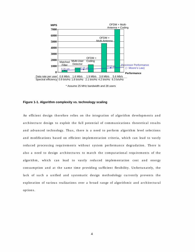
The importance of architecture design is underscored by the fact that algorithm
complexity has been increasing faster than Moore’s Law if the architecture is not
adapted to exploit the improved characteristics. Figure 1 depicts a few representative
communications algorithms with their computational requirements and performance. A
state-of-the-art digital signal processor in 0.25 mm technology can barely meet the
throughput requirement of a high-speed matched filter, and purely relying on
technology scaling will continue to have such a processor which falls short of
computational capability for more advanced algorithms which are demanded by
wireless systems in the near future.
4
0
1000
2000
3000
4000
5000
6000
7000
Performance
MIPS
0.8 Mb/s 0.9 b/s/Hz
1.6 Mb/s1.8 b/s/Hz
1.9 Mb/s2.1 b/s/Hz
3.8 Mb/s4.2 b/s/Hz
5.6 Mb/s 6.3 b/s/Hz
Data rate per user Spectral efficiency
* Assume 25 MHz bandwidth and 28 users
MatchedFilter
Multi-UserDetector
OFDM +Coding
OFDM + Multi-Antenna
OFDM + Multi- Antenna + Coding
Processor Performance(~ Moore’s Law) 0.25 um 0.18 um 0.12 um
Figure 1-1. Algorithm complexity vs. technology scaling
An efficient design therefore relies on the integration of algorithm developments and
architecture design to exploit the full potential of communications theoretical results
and advanced technology. Thus, there is a need to perform algorithm level selections
and modifications based on efficient implementation criteria, which can lead to vastly
reduced processing requirements without system performance degradation. There is
also a need to design architectures to match the computational requirements of the
algorithm, which can lead to vastly reduced implementation cost and energy
consumption and at the same time providing sufficient flexibility. Unfortunately, the
lack of such a unified and systematic design methodology currently prevents the
exploration of various realizations over a broad range of algorithmic and architectural
options.
5
1.2 Research goals
The goal of this research is to bring architecture design together with system and
algorithm design and technology to obtain a better understanding of the key trade-offs
and the costs of important architecture parameters and thus more insight in digital
signal processing architecture optimization in order to facilitate efficient implementation
of high-performance digital signal processing algorithms. The research is focused on
one of the key units in any wireless system: the receiver in portable devices, which has
stringent energy consumption and cost constraints. The results are extendable to other
DSP systems.
A front-end design methodology to facilitate algorithm/architecture exploration of dedicated hardware The proposed front-end design methodology provides efficient and effective feedback
between algorithm and architecture design. The major strategies are:
• Use block diagram based algorithm description composed of coarse-grain
functions to drive the design process. The description reveals the inherent
structures of algorithms such as parallelism, based on which algorithm
characteristics are extracted to assist algorithm selection and architecture
exploration. The algorithm evaluation metrics include not only the traditional
performance measures, but also the suitability for low-power implementation.
• Estimate implementation costs to assist architecture design and give feedback to
algorithm development. First order comparisons of different architectural
implementations of different algorithms are used to narrow down the available
choices without investing large design efforts. Then more accurate
implementation estimation and analysis are used to make final decisions.
Efficient high-level implementation estimation is the key for architecture
exploration.
6
• Use modular implementation approach, which preserves the structures of
algorithm to establish connections between algorithm, architecture and physical
level for high predictability and quick feedback, enables designing and handing
over to back-end design flow at higher level, and increases productivity through
reusing building blocks. A direct mapped approach and a pre-characterized
module library are centric to this approach, where each coarse gain function of
the algorithm is mapped to a highly optimized dedicated hardware. Performance,
power and area estimations are based on module characterization and modeling.
An interactive environment with high-level implementation estimation and evaluation is
developed to assist systematic architecture explorations. This methodology is integrated
in the Berkeley Wireless Research Center (BWRC) design environment and BWRC
design drivers are used to evaluate the effectiveness of this methodology.
DSP architecture design of digital signal processing blocks Multiple orders of magnitude gain in both energy and area (cost) efficiency can be
obtained by using dedicated hardwired and highly parallel architectures (achieving
1000 MOPS/mW and 1000 MOPS/mm2) compared to running software on digital signal
processor. The significant differences are studied and analyzed for a more energy and
area efficient design approach for the signal processing domain of interest, given the
underlying state-of-the-art IC technology.
The main disadvantage of purely dedicated architecture is its inability to provide
flexibility required at system level. There is a fundamental trade-off between efficiency
and flexibility and as a result, many programmable or reconfigurable designs incur
significant energy and performance penalties compared to fully dedicated solutions. The
goal is to reduce this cost of flexibility by combining the system design, which identifies
a constrained set of flexible parameters to reduce the associated overhead, and an
architectural implementation, which exploits the algorithm’s structure and modularity.
7
Algorithm/Architecture co-design of wireless communications systems For each digital signal processing block, the task is to choose an algorithm together
with a matching architecture by trading off the required performance and
implementation costs. At the system level, the challenge is to put blocks together to
perform the entire receiver functionality and the design trade-off is between overall
system performance and implementation costs with the emphasis on block level
interaction. The advantages of bringing together system, algorithm, architecture, and
circuit design are demonstrated by example designs of wireless communications
systems: multi-user detection for CDMA system, multiple antenna processing, OFDM
system, and a multi-carrier multi-antenna system, which all show that optimized
architectures achieve orders of magnitude improvement in terms of both area and
energy efficiency compared to other common DSP solutions.
1.3 Thesis organization
This thesis is organized into six chapters. Chapter 2 presents the algorithm and
architecture exploration methodology, which includes algorithm properties
characterization, architecture evaluation, low-power design techniques, and the front-
end design flow and implementation estimation for dedicated architectures.
Chapter 3 applies the proposed design methodology to two block design examples: an
adaptive multi-user detector in a CDMA system and an interference suppression and
signal combining technique for a multi-antenna system. Different algorithms and
architecture are explored and the results are analyzed.
Chapter 4 addresses the flexibility issue by discussing the flexibility and efficiency
trade-off and proposing a function specific design approach to provide sufficient
flexibility with dedicated architectures. Design examples are given to demonstrate this
approach and compare to other solutions.

8
Appendix A reviews the architectural designs of several DSP kernels, which are key
building blocks for communications systems. And Chapter 5 puts the blocks together,
presents a system design framework for multi-carrier, multi-antenna systems, and gives
example designs with performance simulation results.
Chapter 6 concludes with a summary and suggestions for future work.

9
Chapter 2
Algo r i thm/Arch i te c tu re Exp l o rat i on
2.1 Introduction
Often there exist various digital signal processing algorithms for solving a specific
mathematical problem, but they exhibit vastly different characteristics and thus may
lead to widely different implementation costs. For the same algorithmic specification a
broad range of computational architectures, ranging from general-purpose digital signal
processor (DSP) to dedicated hardware, can be used, resulting in several orders of
magnitude difference in required silicon area and power consumption. Within the realm
of dedicated hardware, the amount of parallelism, the degree of time-sharing of the
processing elements and their structure, as well as various parameters such as word-
lengths, clock frequency, and supply voltage need to be determined. The multi-
dimensional design space offers a large range of possible trade-offs and since decisions
made at each step are tightly coupled with other choices, an integrated and systematic
design approach across the algorithm, architecture, and circuit levels is essential to
optimize the implementation for given design criteria.

10
The results published in [Keutzer94, Rabaey96, Landman96, Raghunathan98] have
made it apparent that the most dramatic power reduction stems from optimization at
the highest levels of the design hierarchy. In particular, case studies indicate that high-
level decisions regarding selection and optimization of algorithms and architectures can
improve design metrics by an order of magnitude or more, while gate and circuit level
optimizations typically offer a factor of two or less improvement. And the design time
involved at high levels is typically much shorter than lower levels. It is thus important
to be able to analyze the possibilities and trade-offs of high-level decisions, before
investing effort in exploration at lower levels. This suggests that architectural
implementation estimation mechanisms are needed to facilitate rapid high-level design
exploration, especially when the goal is to achieve an area efficient, low-power
integrated circuit implementation. Specifically, optimization efforts should begin at the
algorithm/architecture level, which is the focus of this chapter.
2.2 Design space exploration
At algorithm development stage, algorithm performance has often been treated as the
single most important design criterion to evaluate and choose among possible
algorithms, while complexity is considered very roughly. For example, floating-point
operation count (FLOP) is often used as a complexity measure, which is not sufficient
for accurate estimates of power consumption and area. However, design decisions
made at algorithm level affect the implementation significantly. Even for a given
algorithm, many optimization techniques can be applied to, for example, increase speed
and thus allow lower supply voltage. Some of these techniques are common to all
architectures and some are architecture specific. Moreover, although IC technology has
improved to the point that complex wideband receiver systems can now be implemented
for portable devices, with ever more algorithmic complexity, not all algorithms will be
possible to integrate now or even in the near future, since it is unlikely that the

11
improvement in technology will surpass the historical gains of Moore’s law. This
complexity limit comes from the energy and cost (silicon area) constraints of typical
portable applications.
A methodology is therefore needed to assist algorithm exploration, which determines the
feasibility of algorithms for implementation and gives guidance to algorithm developers
about the present and future capabilities of IC technology. This methodology should
evaluate algorithms in terms of not only the traditional measures of performance issues
such as throughput and BER, but also the energy and area requirements.
For a given algorithm, a wide range of computational architecture can be selected. The
difficulty in achieving high energy-efficiency in a programmable processor stems from
the inherent costs of flexibility. Programmability requires generalized computation,
storage, and communication structures, which can be used to implement different
algorithms. Efficiency, on the other hand, dictates the use of dedicated structures that
can fully exploit the properties of a given algorithm. While conventional programmable
architectures, e.g., DSP’s, can be programmed to perform virtually any computational
task, they achieve this flexibility by incurring the significant overhead of fetching,
decoding, and performing computations on a general-purpose data-path under the
control of an instruction stream, which most often dominates the energy dissipation.
The flexibility of programmable processors is highly desirable for handling general
computing tasks. Wireless communication algorithms, on the other hand, have many
distinguishable intrinsic properties that make them more amenable to efficient
implementations and they do not require the full flexibility of a general-purpose device.
These algorithms are data-path intensive, which encourages many digital signal
processing optimization techniques; exhibit high degrees of concurrency, which makes
parallel processing possible; and are dominated by a few regular computations that are

12
responsible for a large fraction of execution time and energy, which suggests the use of
highly optimized and parameterized kernel modules.
There is a wide spectrum of application specific architectures, which sit at different
positions in the trade-off between efficiency and flexibility. While dedicated
implementation and general-purpose microprocessors are at the two extremes
respectively, many domain specific processors fill in the gap between them.
Consequently, a methodology is needed to evaluate architectures to facilitate
architectural level exploration and optimization, such as designing parallel data paths
and memory structures, and choosing programmable granularity. This is an important
step in the design process in order to make a better use of available IC technology and
to realize the potential of advanced communication theoretical results, which usually
require even more processing.
To summarize, high-level design decisions include the choice of algorithm for a given
application specification, the selection of the computational architecture and the
determination of various implementation parameters. Because of the size and
complexity of the multi-dimensional design space, the designer often cannot adequately
explore many of these possibilities, which offer a large range of trade-offs. Therefore,
there is a need for a methodology for high-level algorithm and architecture exploration
and implementation estimation, which feeds back meaningful design guidance and
evaluation of the impact to the designer. Based on the estimated bottleneck of
implementation (e.g., memory bandwidth or execution unit speed), algorithm and
architecture level decisions can be made and optimization techniques can be applied in
a more informed and systematic way to achieve an area-efficient, low-power
implementation. At the same time, the effects of any algorithmic and architectural
modification on system performance must be evaluated to ensure performance goals.

13
The subsequent sections describe the main components of this algorithm/architecture
co-design methodology: algorithm and architecture level design characterization, design
metric identification, optimization techniques (especially for low-power designs), and
high-level implementation estimation methods.
2.3 Algorithm exploration
Much research has been done towards automated behavioral-level synthesis,
optimization, and performance estimation, with the goal of reducing high-level design
and exploration time. However, they are often not sufficient. At the high level of
abstraction, the degrees of design freedom are often so great as to make full analysis of
design trade-offs impractical. Comprehensive analysis of designs is often prohibitively
time-consuming, as is developing a sufficient understanding of the various design
options and optimization techniques. As a result, designers often search the design
space in an ad-hoc manner and decisions are made subjectively and prematurely,
based on hand-waving or partial analysis as well as factors such as convenience and
familiarity.
In this design methodology, algorithms are evaluated at an early stage based on
extraction of critical characteristics. A key step in realizing the potential advantages
attained by using high-level optimization involves developing a better understanding of
the correspondence between algorithms and various architectures. The design
characteristics that are most directly related to the quality of algorithm-architecture
mappings are identified and used to give valuable hints on how to improve
implementation efficiency as well as the selection. For example, some algorithms have
much higher computational complexity requirements compared to others without
performance gain, thus they can be eliminated regardless of architecture choice for low-
power implementation.

14
The underlying idea behind this property-based algorithm characterization is that a
design can be characterized by a small set of relevant, measurable property metrics
which are related to potential design metrics and can be used to provide guidance
during the optimization of the design. Rather than dealing with the design in its
entirety, the property metrics provide a simpler and more manageable representation.
The algorithm property metrics used in this work are mainly based on the set identified
by [Guerra96], which are summarized as following.
Theoretical capacity and algorithm performance, such as convergence speed and
stability of an adaptive algorithm, are evaluated through closed form analytical solution
and/or simulations. They are well studied by the information theory and signal
processing community. The focus here is on implementation complexity evaluation.
Numerical properties Numerical properties indicate how the algorithm responds to various noise sources,
non-idealities and errors and the resulting performance degradation, i.e., the
robustness of an algorithm.
• Word-length. This includes the dynamic range (the ratio between the largest and
smallest numbers) and precision requirements, which lead to the choice of fixed-
point, block fixed-point, or floating-point implementation.

15
With fixed-point arithmetic, numbers are represented as integers or as fractions
in a fixed range, usually from –1 to 1. With floating-point arithmetic, values are
represented by a mantissa and an exponent as (mantissa x 2exponent). The
mantissa is generally a fraction in the range of –1 to 1, while the exponent is an
integer that represents the number of places that the binary point must be
shifted left or right in order to obtain the value represented. Obviously, floating-
point representation can support wider dynamic range at the expense of
increased implementation cost and power consumption. Block floating-point is a
more efficient technique to boost the numeric range of fixed-point, where a
group of values with different mantissa but a common exponent is processed as
a block of data such that within the block, the operations are simplified to fixed-
point. Truncation, rounding, and overflow will cause finite precision errors in a
fixed-point implementation.
Finite precision requirements not only affect both area and power of digital
processing, it also directly relates to the requirement for A to D converter. This is
evaluated typically through noise analyses and fixed-point simulations. The
word-length is typically chosen such that the performance degradation due to
finite precision is small or tolerable compared to infinite precision.
• Sensitivity to parameters such as step-size, noise levels, and signal distortions.
For example, the sensitivities to analog non-idealities set the requirements on
analog components and have a large impact on the final implementation. These
properties are evaluated through complete system end-to-end simulations
including the modeling of various non-idealities.
Size This class of metrics quantifies the amount of computation. Intuitively, the larger the
computation, the more power consumption and longer delay one expects.
• Number of operations of each type (e.g., addition, shift, sample delay, constant
multiplication, variable multiplication) and word-lengths for each operation type.
To a first-order approximation, operation count gives an indication of the
required hardware resources and power consumption. The number of variable
multiplications, in particular, is a common metric used in comparing DSP
algorithms.
16
• Number of array write and read accesses. This is linked to the amount of
memory accesses and storage needed.
• Number of inputs and outputs. This gives an indication of the required input-
output bandwidth.
• Number of constants. This gives an indication of the amount of storage that
must be allocated for constants, which must be preserved for the life-time of the
computation.
• Number and types of operator types (e.g., addition, shift, multiplication) and
data transfer types (e.g., add-to-shift, shift-to-multiply). This gives an indication
of types of hardware and interconnections needed.
To assist the evaluation of size (complexity), basic operation rate is used as a first-order
metric. A basic operation is defined as addition, and all other operations (shift,
multiplication, data access, etc.) are normalized to the basic operation. The weighting
factor of each operation type is based on its relative energy consumption per operation
for a technology. Since energy consumption per operation also depends on the
implementation style, each operation type can be sub-divided. For example, data access
can be based on registers, FIFO’s or SRAM’s, which have very different energy
consumption per access. The basic operation rate metric can be obtained by algorithm
profiling and it can be used together with the energy efficiency of basic operation (about
2000 million 16-bit basic operations per second per mW in a 0.25 µm technology) to
determine the lower bound of power consumption for an algorithm. This lower bound
not only provides an implementation feasibility measure to algorithm developers, but
also provides a comparison base to evaluate any architectural implementation.
Regularity Structured and regular designs are highly desirable for complex VLSI systems. These
properties lead to a cell-based design approach where complex systems are constructed
through repeated use of a small number of primitive or basic building blocks, resulting
in modular and extendable designs. The developments of vector, systolic and wave-front

17
processors [Hwa84, Kun84, Kun88] are examples of the efforts to effectively exploit
computation regularity. The following metrics are used to quantify the intuitive notion
of regularity.
• Size divided by descriptive complexity. The size is the total number of operations
and data transfers executed in the computation. The descriptive complexity is a
heuristic measure of the shortest description from which the signal flow graph
can be reproduced. Intuitively, since a graph with a repeated pattern is easy to
describe, that is an inverse proportional relation between regularity and
descriptive complexity. In comparing two graphs with the same complexity but
different sizes, the larger would be considered more regular, thus establishing
the proportional relation between regularity and size. The heuristic graph
complexity measure can be quantified by the length of a program in a pseudo-
descriptive language which has two primary instructions: instantiate and
connect [Guerra96]. And the length is defined as the total number of instantiate
and connect statements.
• Percentage operation coverage by common templates. For example, the common
templates can be a set of patterns containing chained associative operators. The
coverage can give an indication of the potential for improvement through
grouping and applying optimization techniques using the associative identity to
the patterns.
Locality The concept of locality has been heavily studied and utilized in designs such as memory
hierarchies. Locality is the qualitative property of typical DSP programs that 90% of
execution time is spent on 10% of the instructions. In the computer architecture
domain, temporal locality describes the tendency for a program to reuse data or
instructions that have been recently used and spatial locality describes the tendency for
a program to use data or instructions neighboring those recently used. In the VLSI
signal processing domain, temporal locality characterizes the persistence of the
computation’s variables and spatial locality measures the communication patterns
between blocks and indicates the degree to which a computation has natural isolated

18
clusters of operations with few interconnections between them. Identification of
spatially local sub-structures can be used to guide hardware partitioning and minimize
global buses, which can lead to smaller area, lower bus capacitance, and thus lower
interconnect power. The classification of recursive algorithms, as having either
inherently local or global communications has been used as an indicator of an
algorithm’s suitability for VLSI implementation [Kun88]. The following metrics are used
for quantifying temporal locality and spatial locality:
• Average variable lifetime. A computation is temporally local if its variables have
short predicted lifetimes. Variables with short predicted lifetimes are good
candidates for storage in registers instead of memory.
• Number of isolated components.
• Number of bridges.
• Connectivity ratio. It is the number of internal data transfers divided by the total
possible data transfer.
Concurrency and uniformity Another very important structure is an algorithm’s inherent concurrency, which
measures the number of operations that can be executed concurrently. Concurrency
has been studied extensively and its application has resulted in greatly improved
performance in terms of metrics such as throughput and latency. Concurrency includes
explicit parallelism, which is revealed by data dependency graph or a block diagram
based description, and potential parallelism achievable through pipelining and
chaining, which depends on the internal implementation structure of a block. While
this inherent parallelism cannot be fully exploited by all architectures, it is an
important factor to guide architecture exploration.
• Ratio of the number of operations to the length of the longest path. This is a
rough indicator of the average concurrency.
19
• Concurrency of operations can be quantified by the maximum height of
operation distribution graph, which measures the number of operations
executed in each clock cycle. Concurrency of accesses to registers and
concurrency of data transfers can be quantified in a similar way.
The uniformity characterizes the degree to which resource accesses are evenly
distributed over the course of the computation. For programmable architectures, these
metrics indicate the utilization of each unit. Uniformity can be quantified by the
variance of the distribution graph. In general, the greater the variance, the less uniform
the structure.
Timing The timing metrics assume that each operator has an associated delay of execution. The
hardware library may be user-defined to contain approximated relative delays, which
allows the designer the opportunity to experiment without having to actually design the
modules. The exploration finally leads to the timing specification for each module. The
timing metrics give a measure of how constrained the design is.
• Longest path. This metric, in the number of nodes and edges, is a rough
indicator of overall timing.
• Critical path. This determines the time it takes to complete an iteration of the
computation. The critical path can be found in linear time with a modified
shortest-paths algorithm [Cormen90]. The inverse of critical path gives the
maximum throughput at which the computation can be directly implemented.
• Latency. This is the delay from the arrival of a set of input samples to the
production of the corresponding output. This is measured as the number of
pipelined stages * sample period.

20
• Iteration bound and ratio of iteration bound to critical path. It is defined as the
maximum, over all feedback cycles, of the total execution time divided by the
number of sample delays in the cycle. (The iteration bound for non-recursive
computations is 0.) Iteration bound metrics are related to the potential
improvement in throughput by applying transformations such as pipelining,
retiming, and time-loop unfolding.
• Ratio of the sample period to the critical path.
• Maximum operator delay.
• Slacks for each operator type. They give an idea of how much flexibility the
scheduler has, if there is one as for time-sharing architectures or how much the
block performance can be reduced for energy consideration.
Other topology properties Topology metrics quantifies features related to the interconnection of nodes in a signal
flow graph, without regarding to functionality. Besides the ones presented above, there
are
• Average node fanout. High average fanout may indicate the need for increased
buffering stages.
• Percentage of operations in feedback cycles. It is well-known that any section
without feedback can be easily optimized for throughput, however, cyclic
sections of a computation need special attention.
2.4 Architecture exploration
Given an algorithmic specification, a designer is faced with selecting the computational
architecture, as well as determining various parameters such as the amount of
parallelism, the pipelining scheme, memory design, interconnect structure, clock
period, and supply voltage. Since it requires too much effort and is too time-consuming
to complete all design choices and make final comparisons, fast high-level evaluation is
needed for architectural exploration. The architecture evaluation includes two parts:
selecting a set of design metrics for fair comparisons among different implementations

21
and adopting or developing accurate implementation estimation mechanisms for
meaningful results. These two parts are presented in the following sections.
The architectures being considered include digital signal processors (DSP), dedicated
hardware, and intermediate architectures commonly used in signal processing domain.
Two parameters are used to categorize architectures: the granularity of processing
elements and the amount of time-multiplexing. Granularity gives a measure of the
flexibility an architecture can provide: the larger the granularity, the less the flexibility.
Figure 2-1 depicts the relative positions of different architectures in this two-
dimensional space, which indicates the trade-offs between flexibility, energy efficiency
and area efficiency.
Time-Multiplexing
Granularity of Flexibility Clusters of data-pathsBit-level operations
Application Specific Processor(DSP Extension)
Time-Multiplexing Dedicated Hardware or
Function-Specific Reconfigurable Hardware
Data-path operations
Fully Parallel Direct Mapped
Hardware
Hardware Reconfigurable
Processor (Pleiades)
Software Programmable Digital Signal
Processor
Fully Parallel Implementation on
Field Programmable Gate Array
Time Multiplexing Implementation on
Field Programmable Gate Array
Data-Path Reconfigurable
Processor
Gates
Programmable Array Logic
Figure 2-1. Architecture design space
The amount of time-multiplexing can be measured by the ratio of clock frequency to the
required data processing throughput. The higher degree of time-multiplexing, the faster
the circuits need to run in order to maintain the throughput. The first order costs of
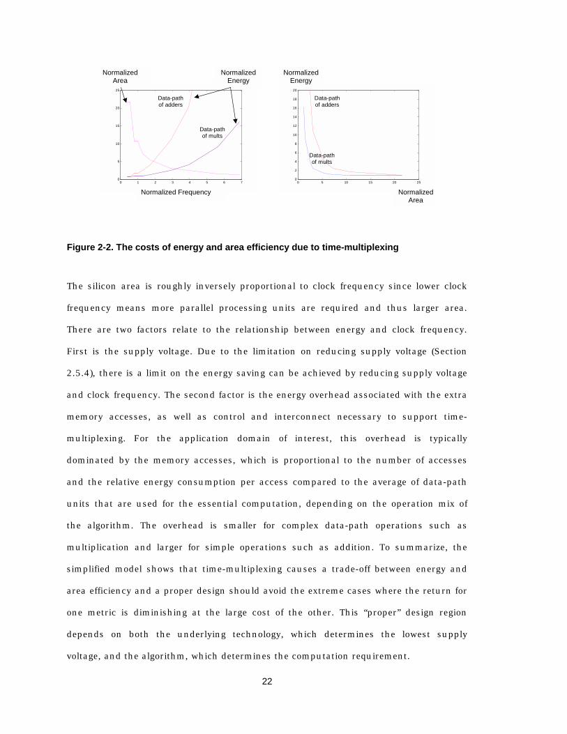
energy and area due to time-multiplexing structures are depicted in Figure 2-2, where
the data are based on the characterizations of data-path units in a 0.25 µm technology.
22
0 1 2 3 4 5 6 70
5
10
15
20
25
0 5 10 15 20 250
2
4
6
8
10
12
14
16
18
20
Data-path of adders
Normalized Frequency
Normalized Area
NormalizedEnergy
Normalized Energy
Normalized Area
Data-path of mults
Data-path of adders
Data-path of mults
Figure 2-2. The costs of energy and area efficiency due to time-multiplexing
The silicon area is roughly inversely proportional to clock frequency since lower clock
frequency means more parallel processing units are required and thus larger area.
There are two factors relate to the relationship between energy and clock frequency.
First is the supply voltage. Due to the limitation on reducing supply voltage (Section
2.5.4), there is a limit on the energy saving can be achieved by reducing supply voltage
and clock frequency. The second factor is the energy overhead associated with the extra
memory accesses, as well as control and interconnect necessary to support time-
multiplexing. For the application domain of interest, this overhead is typically
dominated by the memory accesses, which is proportional to the number of accesses
and the relative energy consumption per access compared to the average of data-path
units that are used for the essential computation, depending on the operation mix of
the algorithm. The overhead is smaller for complex data-path operations such as
multiplication and larger for simple operations such as addition. To summarize, the
simplified model shows that time-multiplexing causes a trade-off between energy and
area efficiency and a proper design should avoid the extreme cases where the return for
one metric is diminishing at the large cost of the other. This “proper” design region
depends on both the underlying technology, which determines the lowest supply
voltage, and the algorithm, which determines the computation requirement.
23
Granularity of flexibility can be measured by the number of gates in each processing
element. The ability to exploit architectural granularity depends on algorithm
requirements. For example, results in [Tuan01] showed that programmable logic array
structure is more suitable (less equivalent gate count and less power) for control finite
state machines compared to field programmable gate array, which is more suited for
signal processing due to its higher configuration granularity. Using finer granularity is
more flexible at the cost of increased energy consumption and area due to the increased
amount of interconnects and switches, which is proportional to (total number of
operations / granularity of processing elements)α (α >=2), as well as the overhead of
over-designing each processing elements in order to provide programmability or
reconfigurability. Choosing a larger granularity by grouping the computational elements
enables optimizations within that group, such as using wires instead of shifters, using a
custom complex multiplier instead of building it from ALU’s, or using FIFO’s instead of
SRAM’s. But at the same time, a larger granularity might decrease the opportunity for
global optimizations as well as reducing the flexibility to map other algorithms onto the
same hardware.
2.4.1 Architecture comparison metrics The most common metrics for DSP architecture comparisons are: performance (= the
time required to accomplish a defined task), power consumption and cost. Many factors
have direct impact on the cost, such as design time (including that for both software
and hardware development), integrated circuit fabrication and testing cost, packaging,
and quantity. In this thesis, cost is simply evaluated as silicon area.
These three metrics are not orthogonal and one can be traded for another. For example,
a commonly used low-power design technique is to use parallel hardware and drop the
supply voltage for fixed throughput (Section 2.5.3). This trades area for power and

24
similarly, performance can be improved with hardware duplication. Moreover, energy
consumption, which determines battery life, is usually more important than power
consumption, which determines the packaging and cooling requirements. For example,
an architecture that can execute a given application quickly and then enter a power-
saving mode may consume less energy for the particular application than other
architectures with lower power consumption. Consequently, the choice of metrics is
important when comparing different architectures. The metrics that will be used in this
thesis are: computation density (= sample rate * silicon area), energy efficiency (= total
energy per computation), and the product of silicon area and power consumption.
Different architectures are often implemented in different IC technologies and operate
with different supply voltages, which directly impact all the metrics being considered.
Therefore, to make a meaningful architecture comparison, the metrics (area, delay, and
power) need to be normalized to a common reference. If device models of the process
technologies are available, accurate transistor-level circuit simulations (e.g., using
SPICE-like simulators) can be performed on standard cells or building logic blocks to
extract the scaling factors. Otherwise, first-order estimates can be derived based on a
few key technology parameters: minimum channel length Lmin, gate oxide thickness Tox,
threshold voltage Vth, and supply voltage VDD, using the following equations [Hu96]:
• Area scaling factor:
2minLArea ∝
• Capacitance scaling factor:
oxoxL T
LTAC
2min∝∝
• Delay (~ 1/clock rate) scaling factor:
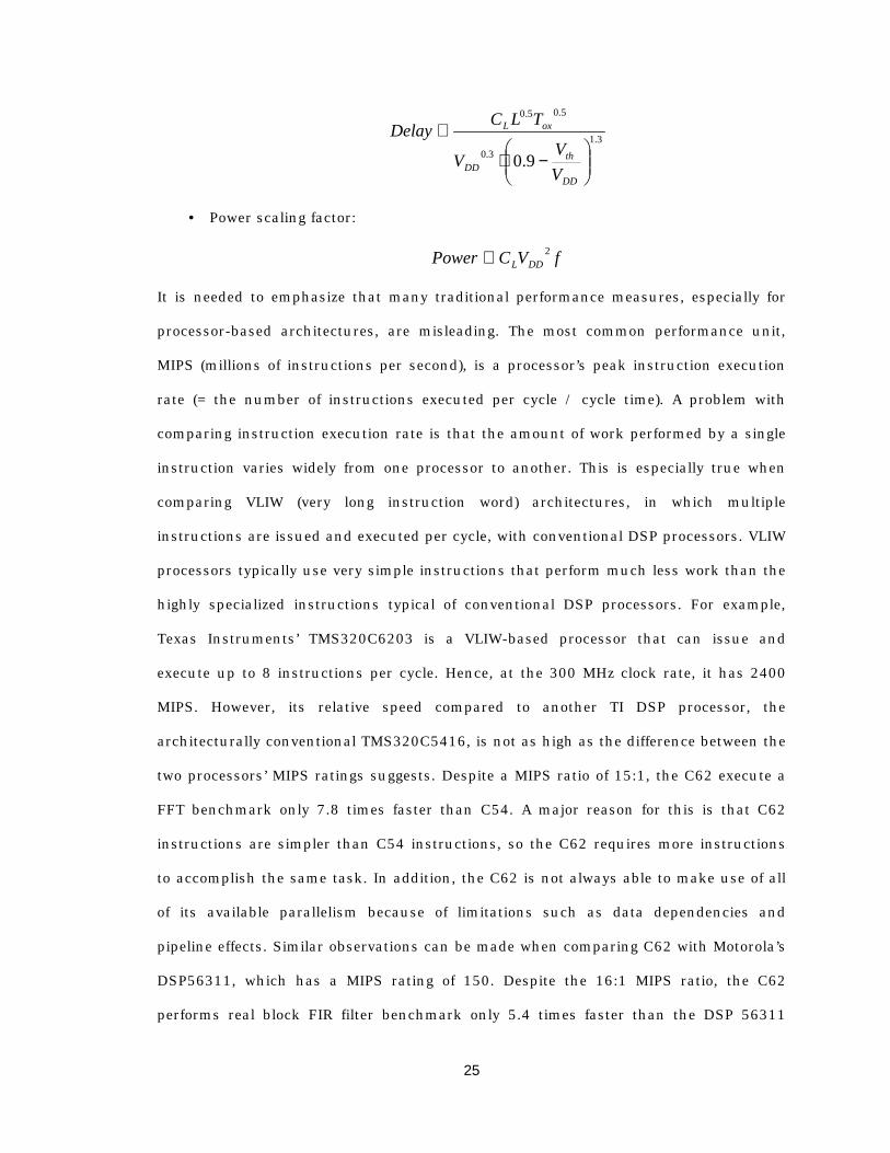
25
3.13.0
5.05.0
9.0
−⋅
∝
DD
thDD
oxL
VV
V
TLCDelay
• Power scaling factor:
fVCPower DDL2∝
It is needed to emphasize that many traditional performance measures, especially for
processor-based architectures, are misleading. The most common performance unit,
MIPS (millions of instructions per second), is a processor’s peak instruction execution
rate (= the number of instructions executed per cycle / cycle time). A problem with
comparing instruction execution rate is that the amount of work performed by a single
instruction varies widely from one processor to another. This is especially true when
comparing VLIW (very long instruction word) architectures, in which multiple
instructions are issued and executed per cycle, with conventional DSP processors. VLIW
processors typically use very simple instructions that perform much less work than the
highly specialized instructions typical of conventional DSP processors. For example,
Texas Instruments’ TMS320C6203 is a VLIW-based processor that can issue and
execute up to 8 instructions per cycle. Hence, at the 300 MHz clock rate, it has 2400
MIPS. However, its relative speed compared to another TI DSP processor, the
architecturally conventional TMS320C5416, is not as high as the difference between the
two processors’ MIPS ratings suggests. Despite a MIPS ratio of 15:1, the C62 execute a
FFT benchmark only 7.8 times faster than C54. A major reason for this is that C62
instructions are simpler than C54 instructions, so the C62 requires more instructions
to accomplish the same task. In addition, the C62 is not always able to make use of all
of its available parallelism because of limitations such as data dependencies and
pipeline effects. Similar observations can be made when comparing C62 with Motorola’s
DSP56311, which has a MIPS rating of 150. Despite the 16:1 MIPS ratio, the C62
performs real block FIR filter benchmark only 5.4 times faster than the DSP 56311

26
[BDTI]. MOPS (millions of operations per second) or MFLOPS (millions of floating-point
operations per second) suffers from a related problem: what counts as an operation and
the number of operations needed to accomplish the useful work vary greatly from
processor to processor.
Some other commonly quoted performance measurement units can also be misleading.
Because multiply-accumulate operations are central to many DSP algorithms, such as
FIR filtering, correlation, and dot-product, MACS (multiply-accumulates per second) is
sometimes used to compare DSP processors. However, DSP applications involve many
operations other than MAC’s and MACS does not reflect performance on other
important types of operations that are present in virtually all applications, such as
looping. Consequently, MACS alone is not a reliable predictor of performance.
Furthermore, most DSP processors have the ability to perform other operations in
parallel with MAC operations, which can have large impact on the overall performance.
2.4.2 Architecture evaluation methodologies For a given algorithm, different architectural implementations can result in orders of
magnitude difference in power consumption and area. It is known that flexibility of
architecture can be traded for efficiency by moving from general-purpose architectures
to more specific architectures. But what is more important is to evaluate the relative yet
quantitative trade-offs in order to make early and meaningful decisions. The first order
comparisons of different architectural implementations of different algorithms are made
to narrow down the available choices without investing large design effort. Then more
accurate implementation estimation and analysis are very important in order to apply
algorithm modifications and transformations and architecture level low-power design
techniques in a more informed manner.
27
Although the most accurate implementation cost assessments should be based on post-
layout circuit simulations (e.g., through Synopsys EPIC tools) or even direct
measurements on the hardware, getting these accurate numbers based on completed
design for a range of architecture choices is impractical. Since algorithm and
architecture level estimations are to be used for guiding design decisions and not for
making absolute claims about the implementation costs, it is only critical that these
estimations give accurate relative information. Since decisions at higher level of
abstraction can result in orders of magnitude difference, this approach provides
meaningful predictions to guide high-level decisions. The estimation methods used for
different architectural implementations are described as following.
Processor based implementation A common approach used to benchmark processors is to use complete applications or
suites of applications [Hennessy96], which is more suited for fair comparisons between
different processor families than MIPS, MOPS, or MACS. This approach is used by the
Standard Performance Evaluation Corporation in the popular SPEC benchmarks for
general-purpose processors. This approach works best in cases where the application is
coded in a high-level language like C. Benchmarking using applications written in a
high-level language amounts to benchmarking the compiler as well as the processor.
Unfortunately, because of the poor efficiency of compilers for most DSP processors and
the demanding real-time performance requirement of the applications, the performance
critical portion of DSP software are typically coded in assembly language. Consequently,
DSP processor performance is often benchmarked based on kernels. Combining
algorithm kernel benchmarking and application profiling is a practical compromise
between oversimplified MIPS-type metrics and overly complicated application-based
benchmarks for DSP performance evaluation.
28
Algorithm kernels are the building blocks of most digital signal processing systems. For
example, the BDTI BenchmarksTM, a basic suite of algorithm kernels, includes 12
functions: real block FIR, complex block FIR, real single-sample FIR, LMS adaptive FIR,
IIR, vector dot product, vector add, vector maximum, Viterbi decoder, control, 256-point
in-place FFT, and bit unpack. The benchmark results for a wide range of DSP processor
can be found at [BDTI]. There are several ways to measure a processor’s performance
on an algorithm kernel benchmark. Cycle-accurate software simulators usually provide
the most convenient method for determining cycle counts. Hardware-based application
development tools can also be used to measure execution time and they are needed to
precisely gauge energy consumption.
Energy consumption is measured by isolating the power going to the DSP processor
from the power going to other system components on a development board, running a
benchmark in a repeating loop, and using a current probe to record the time-varying
current drawn from the supply. Such energy consumption measurements can be time-
consuming and difficult.
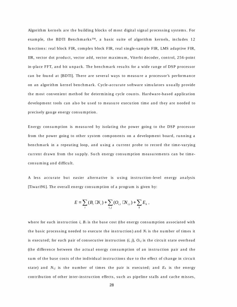
A less accurate but easier alternative is using instruction-level energy analysis
[Tiwari96]. The overall energy consumption of a program is given by:
∑∑∑ +⋅+⋅=k
kji
iiiii
ii ENONBE,
,, )()( ,
where for each instruction i, Bi is the base cost (the energy consumption associated with
the basic processing needed to execute the instruction) and Ni is the number of times it
is executed; for each pair of consecutive instruction (i, j), Oi,j is the circuit state overhead
(the difference between the actual energy consumption of an instruction pair and the
sum of the base costs of the individual instructions due to the effect of change in circuit
state) and Ni,j is the number of times the pair is executed; and Ek is the energy
contribution of other inter-instruction effects, such as pipeline stalls and cache misses,
29
which would occur during the execution of the program. Typically, the energy is
dominated by the first term since effect of circuit state on the energy consumption of
the processor is masked by the much larger common cost to all instructions, such as
clocking, instruction fetching, memory arrangement, pipeline control, etc. The cost data
can be obtained by executing a loop consisting of several instances of the given
instruction or instruction pair. For example, Texas Instruments provides application
notes [TI] that detail power consumption of each instruction type under certain
processor configurations. Unfortunately, most DSP processor vendors publish only
“typical” or “maximum” power consumption numbers. In those cases, the only method
is to obtain a credible estimate of power consumption, which is based on computation
intensity of the benchmark, and multiply it by the execution time.
The results of algorithm kernel benchmarks are useful but incomplete without an
understanding of how the kernels are used in actual applications. Application profiling
at the algorithm kernel (or instruction) level can be used to relate algorithm kernels to
actual application. Profiling provides the number of times key algorithm kernels are
executed when an application is run. This can be done in a number of ways. From code
in high-level languages such as C, kernel-profiling information can be obtained by
identifying subroutines. From assembly code, profiling can be achieved by running the
code on an instruction set simulator. Profiling information can also be estimated by
studying block-level signal flow graphs.
A processor’s performance and energy consumption on an application is estimated by
combining the results of benchmarks with the results of the application profiling.
Multiplying the benchmark execution times by the number of occurrences of each
benchmark (or a similar algorithm kernel) yields an estimate of the time required to
execute the application. The same method applies to calculating total energy
consumption.
30
After obtaining some baseline number of implementation estimates of an algorithm on
an existing processor architecture, the relative improvements by adding architecture
extensions can be evaluated for application specific processors. For more accurate
estimation, DSP architecture evaluation tools, such as [Ghazal99], can be used, which
is based on high-level algorithm description and aims for estimation within 10%
accuracy compared to using hand optimized assembly code. Some detailed architecture
model needs to be supplied for that purpose.
Reconfigurable hardware For reconfigurable hardware, evaluations have been done for different architecture
templates, such as Pleiades [Wan00] and Philips’ stream-based data flow architecture
[Kienhuis99], which can give implementation estimations at different levels based on
template matching.
Dedicated hardware Since dedicated hardware is most flexible in terms of architecture parameter choices,
e.g., parallelism and pipelining structures, even the first order estimations have to be
based on predictable physical implementation. And due to its dedication to one
application (hardwired structure), by adding refinement to the architecture design,
accurate implementation estimation can be obtained. An estimation methodology was
developed as part of a front-end ASIC design flow, described in section 2.6.
2.5 Low-power design techniques
Motivated by emerging battery-operated applications that demand intensive
computation in portable devices, techniques have been investigated to reduce energy
consumption in CMOS digital circuits, or equivalently power consumption while
maintaining computational throughput.

31
2.5.1 Sources of power dissipation There are three major sources of power dissipation in digital CMOS circuits:
ddleakageddscclkddL
leakagecircuitshortswitchingtotal
VIVIfVVCPPPP
++α=++= −
.
The first term represents the switching component, where α is the activity factor (= the
probability that a power-consuming transition occurs), CL is the loading capacitance,
and fclk is the clock frequency. In most cases, the voltage swing V is the same as the
supply voltage Vdd. The second term is due to the direct-path short circuit current Isc,
which arises when both the NMOS and PMOS transistors are simultaneously active.
The third term, leakage current Ileakage, arises from substrate injection and sub-
threshold effects, which is primarily determined by fabrication technology. The
dominant term in a properly designed circuit is the dynamic power associated with the
charging and discharging of the parasitic capacitance, resulting in an energy per
operation cost of 2ddeffop VCE = , where Leff CC α= is the effective capacitance being
switched and is different for each operation.
Any low-energy design techniques are thus based on minimizing Ceff and Vdd, while
retaining the required functionality and throughput. Notice that in contrast to general
purpose computing, where the goal is often to provide the fastest possible computation
without bound, a common concept in dedicated real-time digital signal processing is
maintaining a given computation throughput since there is no advantage in performing
the computation faster than the given rate.
32
2.5.2 Algorithm level optimization Many low-power design techniques can be applied at multi-levels to vastly reduce the
energy consumption. At algorithm level, an optimization may involve performing
algorithm modifications, selecting new arithmetic operations, or applying
transformations. Transformations involve changes in the structure of an algorithm
without changing the input-output behavior, while the number and type of
computational modules, their interconnection and their sequence of operation are
optimized. Numerous algorithmic transformations were presented in [Chandrakasan95]
to reduce energy, which were categorized into two key approaches. The first one is
enabling the reduction of the supply voltage through application of speed-up
transformations. The second one utilizes transformations to reduce the effective
capacitance being switched.
The basic idea for speed-up transformations is the reduction of the number of control
steps required by the algorithm, which is often possible through the exploration of
concurrency. The transformations that are most suitable to increase the degree of
concurrency of an algorithm include retiming, functional pipelining, algebraic
manipulations, and loop restructuring (e.g., loop unfolding and software pipelining).
Generic transformations to reduce Ceff involve, for example, algebraic transformations
using the associative, distributive and commutative identities to reduce the total
number of operations required, the substitution of some operations with more
convenient ones, i.e., strength reduction depending on the cost functions of operation
types on a particular architecture (such as constant propagation and replacement of
constant multiplications with additions and shifts), the optimization of the resource
usage, and a reduction of the word-length required for data representation.
Moreover, some modifications can be applied to the algorithm in order to make
algorithm properties more suitable for low-energy implementation. For instance,

33
feedback loops often become the bottleneck in a recursive algorithm. Adding delays in
the loop can shorten the critical path and increase concurrency, thus providing more
opportunity to maintain throughput at reduced voltage through pipelining. However,
modified algorithms need to be re-evaluated to ensure that there is no overall system
performance degradation.
While an effective sequence of optimization techniques has important impacts on the
optimization result, finding an appropriate sequence is often not easy. As a result, high-
quality designs often require customized optimization obtained through exploration of a
variety of potential optimization sequences. An interactive environment for guiding the
design exploration process was developed in [Guerra96] to help designers explore
options and make decisions in a more systematic and informed manner. At each stage,
estimations are used to determine the placement of the current implementation in the
area-throughput-power design space. Using the estimations as guidance, the designer
can choose to apply an optimization technique to improve the solution. Exploration
proceeds with repeated iteration through optimization, module selection, design
characterization and estimation.
2.5.3 Architecture level optimization At the architecture level, the main energy reduction approaches are to optimize
fundamental components, which include computation, communication, and global
variable storage, and to reduce overhead components such as control, interconnect,
and temporary variable storage.
Clearly, the most effective ways of reducing the energy consumption of a circuit is to
reduce the supply voltage due to its quadratic influence on energy. But this drop in
energy consumption comes at the expense of increased delay time and thus slower
circuits, so it is necessary to compensate for this degradation in circuit speed at
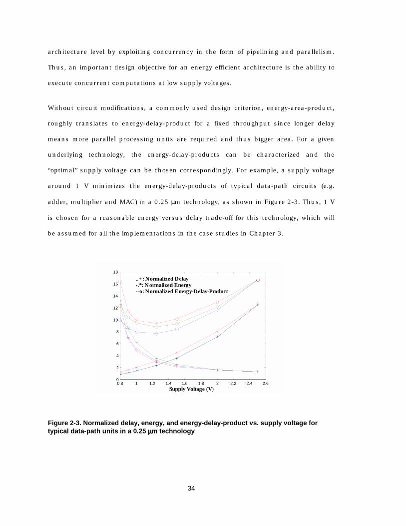
34
architecture level by exploiting concurrency in the form of pipelining and parallelism.
Thus, an important design objective for an energy efficient architecture is the ability to
execute concurrent computations at low supply voltages.
Without circuit modifications, a commonly used design criterion, energy-area-product,
roughly translates to energy-delay-product for a fixed throughput since longer delay
means more parallel processing units are required and thus bigger area. For a given
underlying technology, the energy-delay-products can be characterized and the
“optimal” supply voltage can be chosen correspondingly. For example, a supply voltage
around 1 V minimizes the energy-delay-products of typical data-path circuits (e.g.
adder, multiplier and MAC) in a 0.25 µm technology, as shown in Figure 2-3. Thus, 1 V
is chosen for a reasonable energy versus delay trade-off for this technology, which will
be assumed for all the implementations in the case studies in Chapter 3.
0.8 1 1.2 1.4 1.6 1.8 2 2.2 2.4 2.6 0
2
4
6
8
10 12 14 16 18
Supply Voltage (V)
..+: Normalized Delay -.*: Normalized Energy --o: Normalized Energy-Delay-Product
Figure 2-3. Normalized delay, energy, and energy-delay-product vs. supply voltage for typical data-path units in a 0.25 µµµµm technology

35
In order to operate at such a low voltage and to still be able to accomplish the real-time
processing rates required for the algorithms, it is necessary to parallelize the
algorithms. This can be accomplished in a number of ways depending on the
computational architecture. One approach, at the maximum flexibility end of the
architecture spectrum, is to use a number of software programmed DSP's. The overhead
of splitting the algorithm into a number of processors can become prohibitive if a large
number of processors are required (e.g. >10). Another approach is to use dedicated
hardware. For example, a direct mapping strategy maximizes the hardware parallelism
by directly implementing the data flow graph of the algorithm onto silicon. While this
method is the most energy efficient, because it removes the overhead associated with
programmability, it is the least flexible.
Some other important techniques to reduce energy consumption are aimed at
minimizing switching capacitance or energy waste. This can be achieved by preserving
locality inherent in the algorithm with distributed storage, interconnect and
computational structures; enforcing a demand-driven policy that eliminates switching
activity in unused modules; and preserving temporal correlation in data streams by
avoiding extensive hardware sharing. Most of these techniques can only be applied with
limited success to conventional programmable architectures that are based on a data-
path executing a large instruction set under the supervision of a global instruction fetch
and decode controller. On the other hand, a dedicated architecture is able to exploit all
these techniques effectively.
The dedicated hardware can also exploit another technique for low-power design by
avoiding wasteful activity associated with over accurate computations. The number of
bits used in the arithmetic strongly affects all key parameters of a design. It is desirable
to minimize the number of bits for energy and area optimizations while maintaining
sufficient algorithmic accuracy and performance.

36
Architecture level optimization techniques [Chandrakasan95b] also include: minimizing
switching activity by the choice of number representation, e.g., using sign magnitude
representation to reduce the number of transitions on busses and activity of arithmetic
computation, ordering of input signal to reduce switching activity, balancing all signal
paths and reducing logic depth to minimize glitching activity, and cautious application
of resource sharing in terms of both busses and execution units to avoid the
destruction of data correlation.
Low-power design techniques based on logic style, circuit, and technology optimizations
were present in [Chandrakasan92, 95b]. These techniques include: choosing logic style
(static, dynamic, or pass-gate), logic function, and circuit topology to reduce spurious
transitions, short-circuit current, parasitic capacitance, and switching activity; using
reduced swing logic; scaling threshold voltage; applying power-down strategies and
gated clocks; optimizing transistor sizes; optimizing placement and route, etc.
In addition, there are software specific techniques to minimize power or energy, which
tend to fall into one or more of the following categories: selection of the least expensive
instructions or instruction sequence, minimizing the frequency or cost of memory
access, and exploiting power reduction features of processor based implementation. A
prerequisite to optimizing a program for low power is to design an algorithm that maps
well to the given processor architecture, the next requirement is to write code that
maximizes performance, exploiting the performance features and parallel processing
capacity of the hardware as much as possible. Maximizing performance also gives
increased latitude to apply other power optimization techniques such as reducing
supply voltages, reducing clock rate or programmable clock (some DSP’s allow the
processor’s clock frequency to be varied under software control and use the minimum
clock speed required for a particular task), shutting off idle components through “sleep”
or “idle” modes, and peripheral control (some DSP’s allow the programmer to disable

37
peripherals that are not in use). energy minimization techniques related to memory
concentrate on one or more of the following objectives: minimizing the number of
memory accesses required by an algorithm; minimizing the total memory required by an
algorithm; making memory accesses as close as possible to the processor; making the
most efficient use of the available memory bandwidth, e.g., use multiple word parallel
loads instead of single word loads as much as possible.
2.5.4 Trade-offs and limits of applying low-power design techniques
First, the most effective way to save energy is to drop supply voltage. But there is a limit
where the circuit delay and the variation due to different process corners increase
significantly as shown in Figure 2-4. (The delay dependence on supply voltage was
verified to be relatively independent of various logic functions and logic styles
[Chadrakasan92].) Consequently, in order to achieve predictable and reliable circuit
performance, a lower bound of supply voltage is chosen to avoid the dramatic increase
of delay.
Second, the design domain has a large impact on the application of various low-power
design techniques. For example, one commonly used technique to maintain throughput
at reduced supply voltage is through hardware duplication. In a digital baseband
receiver for wireless communications systems, the processing throughput is determined
by sample rate or the available bandwidth. Typically the total bandwidth of a wideband
system is about 15-25 MHz and most processing occurs at that rate, with some
processing at much lower rate than the sample rate. Thus the speed requirements of
wireless baseband receivers are relatively slow compared to the transistor switching
speed of a state-of-the-art CMOS technology. For this low-speed application domain,
parallel structures are less effective in reducing energy due to the lower supply bound.
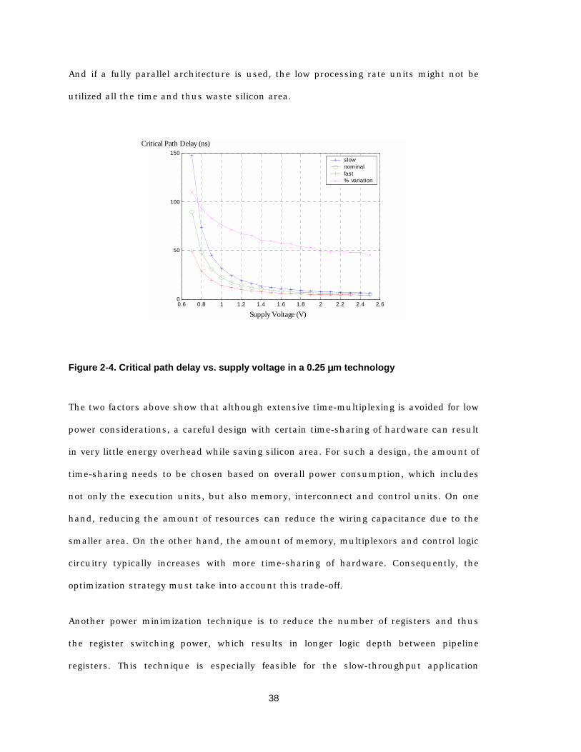
38
And if a fully parallel architecture is used, the low processing rate units might not be
utilized all the time and thus waste silicon area.
0.6 0.8 1 1.2 1.4 1.6 1.8 2 2.2 2.4 2.60
50
100
150slow nominal fast % variation
Supply Voltage (V)
Critical Path Delay (ns)
Figure 2-4. Critical path delay vs. supply voltage in a 0.25 µµµµm technology
The two factors above show that although extensive time-multiplexing is avoided for low
power considerations, a careful design with certain time-sharing of hardware can result
in very little energy overhead while saving silicon area. For such a design, the amount of
time-sharing needs to be chosen based on overall power consumption, which includes
not only the execution units, but also memory, interconnect and control units. On one
hand, reducing the amount of resources can reduce the wiring capacitance due to the
smaller area. On the other hand, the amount of memory, multiplexors and control logic
circuitry typically increases with more time-sharing of hardware. Consequently, the
optimization strategy must take into account this trade-off.
Another power minimization technique is to reduce the number of registers and thus
the register switching power, which results in longer logic depth between pipeline
registers. This technique is especially feasible for the slow-throughput application
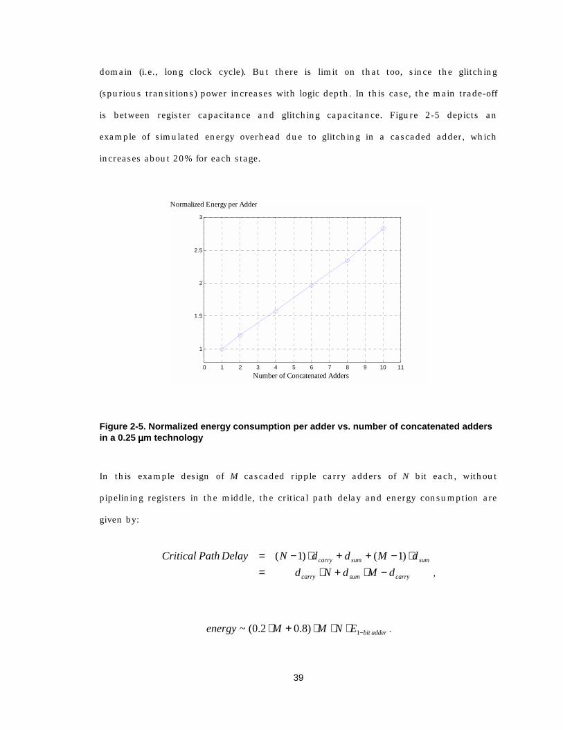
39
domain (i.e., long clock cycle). But there is limit on that too, since the glitching
(spurious transitions) power increases with logic depth. In this case, the main trade-off
is between register capacitance and glitching capacitance. Figure 2-5 depicts an
example of simulated energy overhead due to glitching in a cascaded adder, which
increases about 20% for each stage.
0 1 2 3 4 5 6 7 8 9 10 11
1
1.5
2
2.5
3
Number of Concatenated Adders
Normalized Energy per Adder
Figure 2-5. Normalized energy consumption per adder vs. number of concatenated adders in a 0.25 µµµµm technology
In this example design of M cascaded ripple carry adders of N bit each, without
pipelining registers in the middle, the critical path delay and energy consumption are
given by:
carrysumcarry
sumsumcarry
dMdNddMddNDelayPathCritical
−⋅+⋅=⋅−++⋅−= )1()1(
,
adderbitENMMenergy −⋅⋅⋅+⋅ 1)8.02.0(~ .
40
With P pipeline registers equally distributed in the middle, the critical path delay and
energy consumption become:
carrysumcarry
sumsumcarry
dPMdNd
dPMddNDelayPathCritical
−+
⋅+⋅=
⋅−+
++⋅−=
1
)11
()1(
,
registerbitadderbit ENPENMP
Menergy −− ⋅⋅+⋅⋅⋅++⋅
11)8.01
2.0(~ .
Notice that reducing the logic depth by inserting pipeline registers means reduced
critical path delay, and thus possibly lower supply voltage for fixed throughput. But in
situations where no further voltage reduction is possible, because of either longer
critical path from other circuit or circuit performance variation considerations, the
trade-off between glitching and register power consumption becomes the determining
factor for the design. At certain point, pipeline registers are added not to speed up but
to reduce wasting transitions.
2.6 Design flow and estimation methodology
Many results have demonstrated that algorithm and architecture level decisions have
much larger impact on final implementation compared to lower level optimization
techniques. So the main goal of the design flow is to have a fast and predictable
implementation to facilitate algorithm and architecture level exploration. Since many
existing synthesis approaches have the bottleneck at the feedback from physical
implementation to algorithm/architecture design and thus resulting in very long
iteration loop, a different approach was adopted.

41
First, a block diagram is used for algorithm description and cycle-accurate signal flow
graph is used for architecture design. Also, algorithm and architecture level designs
stay in the same simulation environment so that the impact of any algorithm or
architecture modifications on the whole system performance can be easily evaluated.
Second, between architecture and physical implementation pre-characterized macro
modules are used and the floor-plan of macro blocks is based on algorithm locality. By
preserving algorithm structures, connections are established between algorithm,
architecture, and physical levels resulting in accurate predictability and quick feedback.
This is a major difference from existing synthesis approaches, in which the algorithm is
first decomposed into fine grain operations in an imperative language where algorithm
structures such as locality are lost. Since exploiting those structures can significantly
reduce the energy consumption, many heuristic optimization techniques have been
developed to recover those structures back to improve synthesis results. In the
proposed approach, algorithm structures are not broken throughout the design process.
Lastly, design and hand-over to back-end design flow occur at a high level for higher
productivity with design reuse of the basic building blocks. The following sections
describe the details of the front-end design flow and the methodology.
2.6.1 System specification For the purpose of this research, the criterion for choosing the type of system
description is it should facilitate algorithm and architecture level explorations and
optimizations. This section presents that a block diagram based approach is more
appropriate than commonly used C program based approach.
First, digital signal processing algorithms, especially communications systems, have
special features which can be leveraged in the design approach. They are typically data-
path intensive with predictable execution and dominated by parameterized kernels,
42
such as FIR, vector/matrix operations, CORDIC, FFT, encoder, and decoder.
Consequently, an algorithm can be specified based on a behavioral block diagram,
which is composed of parameterized coarse-grain kernels and simple control flow graph,
so that block level static analysis is sufficient. Signal directives are used to indicate
kernel parameters, such as vector length and matrix size. This specification reveals
algorithm inherent structure and its relatively coarse granularity makes it easier to
develop and specify more complex algorithms. Also, it facilitates the evaluation of all the
important properties of an algorithm listed in Section 2.3, which are related to
implementation cost.
Second, block diagram based algorithm description facilitates architecture level
exploration and optimization as well as implementation estimation through the use of a
library of software kernels and hardware modules. A straightforward way to implement
an algorithm is programming in C and compiling it to a processor. Designing in C, a
sequential language for general-purpose programming, makes it hard to exploit
algorithm properties, such as concurrency, and it depends heavily on the compiler for
data dependency analysis and optimization. Also, it does not take into consideration the
implementation architecture. Assembly optimization can be applied to improve the
design metrics and manually optimized assembly codes are widely used for DSP’s and
have been proven to give many times improvement over compiled codes since designers
have better understanding of the algorithm and architecture. But designing in assembly
is time-consuming and makes it very hard to explore different programmable
architectures. One way to deal with this is to use a block diagram based algorithm
description and build an optimized assembly library for the blocks. This approach is
manageable when the application domain, such as wireless communications
algorithms, has a few dominant blocks. Except possible overhead between blocks, this
approach gives relatively accurate and predictable estimation of a nearly optimized
implementation on a specific processor, as well as suggests possible partition between

43
parallel processors according to algorithm’s inherent concurrency and locality. DSP
vendors, such as TI, and third party groups, such as BDTI, offer optimized kernel
assembly codes on various DSP processors, based on which performance estimates can
be made to help choose the most suitable processor for implementation.
Instruction level parallelism and optimizations can be applied to improve processor
performance by adding application specific instructions and hardware accelerators to
better support dominant operations in the application. The resulting architecture is
often called application specific processor (ASP). These optimizations are typically based
on functional blocks, where each block supports instruction packing or combinations,
memory configurations, and/or specific hardware units which is traded off against their
corresponding cost (area, power, etc.).
A domain specific hardware reconfigurable architecture exploits the parallelism at
macro block level. One example of this kind of architectures is the Pleiades architecture
developed at Berkeley, which is composed of a programmable microprocessor and
heterogeneous computing elements referred as satellites. From a block diagram based
algorithm description, the dominant compute kernels and available concurrency and
data dependency can be extracted, which facilitates the pattern mapping and
scheduling process used for designing this architecture family [Wan00].
In a fully direct mapped architecture, each block is mapped to dedicated logic. Once
again, based on the parameterized module library, a designer can stay at block diagram
level for algorithm and architecture exploration and optimization and obtain predictable
physical implementation.
To summarize, a block diagram based algorithm description is appropriate for signal
processing algorithms (including data-flow and control) and it facilitates the
architecture design and exploration. Compared with a description using high-level

44
sequential language, a block diagram is more natural to algorithm development, since it
provides the proper granularity for algorithm and architecture selection, and reveals the
concurrency information and data dependencies that are inherent in the algorithm
instead of relying on a compiler to figure it out. It also matches well with the
parameterized module library based implementation approach which facilitates reuse of
design knowledge and improves predictability. For each block, models of speed, area
and power on different architectures are characterized based on either assembly kernels
for processor-based implementation, configuration for reconfigurable hardware, or
hardware modules for dedicated design. The library elements will grow with algorithm
needs and architecture choices. In addition, module library based approach also
encapsulates circuit level choices such as choosing an implementation style: FPGA,
standard cell synthesis, or custom design.
The MathWorks’ tool Simulink was chosen as the basis of this block diagram based
description because it is tightly integrated with the popular system design environment
MATLAB. Simulink offers a number of data-path building blocks which help the
development of communications systems. In addition, it offers a graphical language for
describing control flow with state machines, called Stateflow. With both data-path and
control primitives, a discrete-time simulation can be created in Simulink to completely
specify the behavior of a digital signal processing system. The choice of Simulink is
further driven by its compatibility with the simulation of a complete radio, including the
analog components.
2.6.2 Chip-in-a-day design flow A highly optimized dedicated architecture will not be useful unless there is a rapid
implementation strategy. The difficulty of implementing the optimized architectures in a
standard design flows stems from the lack of a consistent flow from a system-level
45
description to the physical layout. A standard design flow has three phases, which are
typically handled by three different engineering teams. System designers conceive the
chip and deliver a specification to ASIC designers, often in the form of a C simulation.
This system level description can be used in a simulation to generate system
characterization curves such as a bit-error-rate vs. signal-to-noise ratio curves for a
communications chip. The ASIC designers map the simulation to VHDL or Verilog code
that they deliver to the physical design team that synthesizes the code to a netlist of
standard cells and interconnection and then uses place and route tools to generate
layout mask patterns for fabrication.
This procedure requires 3 translations of the design with requirements for re-
verification at each stage along with considerable looping. Even more importantly the
opportunities for algorithmic modifications to ease chip performance limitations are
lost, since at the highest level the system designer who could make such algorithmic
modifications does not have information about the chip performance bottlenecks or
power consumption requirements. At the lower levels the information about the
algorithm is essentially lost, so it is very difficult if not impossible to make algorithmic
modifications without returning to the system design level and starting the process over
again.
A design methodology for highly optimized design must eliminate this pipeline and bring
system, ASIC and physical design together if rapid implementation is to be achieved
through high-level automation. The chip-in-a-day design flow [Davis01] provides a
common framework starting from a Simulink description that encapsulates design
decisions spanning all levels in a design process: function level, signal level, circuit
level, and floor-plan level, with arbitrary hierarchy depth. A “push-button” flow is being
developed which will ultimately allow complete translation from the high-level system
description into a chip design ready for fabrication within a day.

46
2.6.2.1 Front-end design flow This thesis is focused on the front-end of the design process, as depicted in Figure 2-6.
The front-end design process includes floating-point modeling and simulation for
algorithm development and initial system performance evaluation, fixed-point modeling
and simulation for algorithm refinement, and cycle-accurate fixed-point modeling,
which is a signal flow graph description of the architecture. All these tasks can be
performed within the Simulink based unified design environment.
Algorithm
Architecture
Estimation and Evaluation
Netlist and Floor Plan of Macro Modules + Standard Cells
Back-end Design flow
Pre-Characterized Module Library
with PDA Models
Data Flow (construct with parameterized
modules) (synthesize to standard cells)
+
Physical Design Information
(generate C code)
Control Flow
Implementation on Processor
System-Level Design Environment
Recommendation for Modifications and Transformations
Figure 2-6. Front-end design flow for dedicated hardware
For algorithm and architecture level deign exploration and optimization, it is important
to provide designers with feedback about the resulting power, delay, and area
estimates. Module-based approach is used to link the algorithm and architecture design
to physical realization and facilitate fast and reliable physical information feedback. The
idea is that the designer can do design using the building blocks and get predictable
results without going down to the physical layer. A pre-characterized, macro-module
47
library is central to this approach. The reason that library approach is feasible is that
DSP applications are dominated by a relatively small number of parameterized kernels.
Each module in the library has a behavioral model for system simulation, possibly
several realizations of the functionality with power-delay-area models for estimation,
and module generator for semi-custom layout generation or standard cell synthesis
script. Algorithm is mapped to architecture using the blocks from the supporting library
and control graph which will be either synthesized to standard cells or implement to an
on-chip processor through code generation by Real-Time Workshop, a tool comes with
Simulink. A netlist generator translates the design and pass it to back-end design flow
along with floor-plan information. The estimation along the refinement path is very
important to provide meaningful guidance for modifications and transformations at
both algorithm and architecture levels, which because of the tight connection to
physical design has a solid base and fast iteration time.
The module library is composed of optimized implementations of commonly used
functions. For instance, a complex dot product is composed of four real multiplication,
one addition and subtraction, and accumulation. A complex MAC module in the library
combines all the operations and is optimally structured and routed. It is also
characterized with predictable delay, and it has low power consumption and small area.
Implementation evaluation and estimation are based on the cycle-accurate signal flow
graph description. Performance estimation checks the critical path to meet throughput
requirements, with total power consumption and silicon area also being estimated.
Starting with a fully parallel architecture, the design is also evaluated for resource
utilization, which can suggest possible hardware sharing. Also, reconfigurability can be
provided by adding local control and interconnect switches. The design iterates until a
satisfactory result is achieved. The key of this approach is designer has full control to
make major architectural decisions at a high level.
48
2.6.2.2 SSHAFT: a back-end ASIC design flow
The goal of the design environment described in [Davis01] is to take an initial Simulink
description of a dedicated architecture and to automatically and rapidly generate the
physical implementation. This environment accelerates the design process by
automating the design flow from a single high-level description to mask layout, which
encapsulates the important decisions typically made by system, ASIC and physical
designers separately during the various stages of the design process.
The back-end design flow is automated with a tool much like the UNIX MAKE program.
The flow begins with a front-end design (algorithm and architecture design in Simulink
composed of modules from a library); it is then converted to an electronic design format,
module generators are invoked, and modules are connected into a hierarchical netlist of
routable objects. Auto-layout views are generated by merging the netlist with the floor
plan, allowing maximal reuse of floor-pan information on successive iterations.
2.6.3 Module generation, characterization and modeling A module library based approach is adopted to provide accurate and predictable energy,
area, and delay estimates. A module can be any arithmetic operations (e.g., complex
MAC, adder, CORDIC), memory blocks (e.g., register file) or interconnect network, which
is either duplicated many times or is a non-negligible part in the design. It can also be a
large composite block such as FFT and Viterbi decoder. The library is evolving with
applications, commonly used or critical random modules will be carefully designed and
characterized and become new modules.
Parameterized data-path modules For DSP systems, the data-path components typically account more than 80% of the
total area and energy. A pre-characterized, parameterized library of macro-cells, based

49
on either custom design or standard cell synthesis was developed. The characterizations
of each module in the library include energy consumption, area, critical path delay, and
input capacitance with parameters such as word-length, supply voltage, loading, and
technology and process corners. The average energy consumed is calculated (which
includes clock load and intra-block interconnect), where the statistics of the applied
data are ignored at this level and a random data model is employed.
To achieve high accuracy, layout and extracted netlist are generated for each data-path
module. Its functionality is verified with the corresponding bit-true and cycle-accurate
Simulink model and an in-house tool called CHARCOAL is used to characterize it
automatically through SPICE-like circuit simulations. Based on simulated data, high-
level models are derived, which can be an analytical expression, look-up table, or graph.
Parameterized modules can be generated by different methods, such as Synopsys’
Design Compiler or Module Compiler or semi-custom tiled layout generators. For
example, four different designs of 12-bit complex multiplier are compared in Table 2-1
(VDD = 1 V and f = 25 MHz).
Style Area [µm!µm] Power [mW] Critical Path [ns]
1 500!500 0.824 23.5
2 485!485 1.572 19.2
3 664!564 0.928 36.2
4 432!418 1.230 16.4
TABLE 2-1. Performance comparisons of 12b!!!!12b complex multipliers
All the designs have an internal pipeline stage, where style 1 is a semi-custom design
though tiling of custom leaf cells, style 2 is a hand-optimized Verilog standard cell
design, style 3 is a composite design built by using custom designs (4 real multipliers,
one adder, and one subtractor), and style 4 is a synthesized design using Synopsys
data-path synthesis tool. This comparison shows that with improved data-path
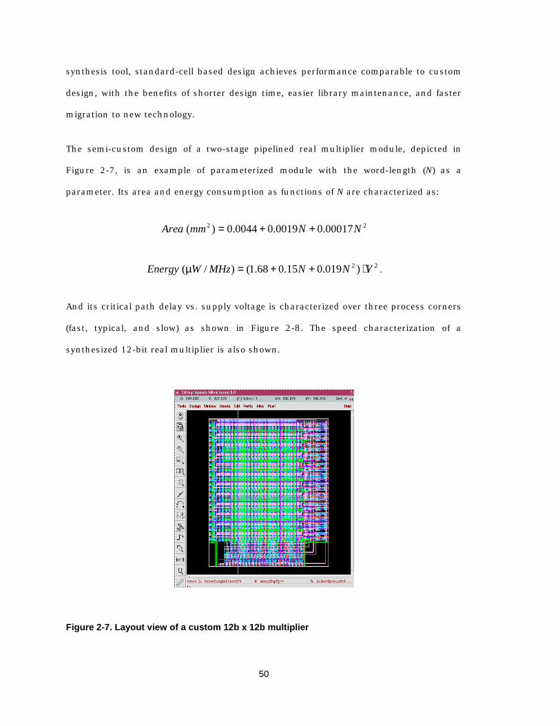
50
synthesis tool, standard-cell based design achieves performance comparable to custom
design, with the benefits of shorter design time, easier library maintenance, and faster
migration to new technology.
The semi-custom design of a two-stage pipelined real multiplier module, depicted in
Figure 2-7, is an example of parameterized module with the word-length (N) as a
parameter. Its area and energy consumption as functions of N are characterized as:
22 00017.00019.00044.0)( NNmmArea ++=
22 )019.015.068.1()/( VNNMHzWEnergy ⋅++=µ .
And its critical path delay vs. supply voltage is characterized over three process corners
(fast, typical, and slow) as shown in Figure 2-8. The speed characterization of a
synthesized 12-bit real multiplier is also shown.
Figure 2-7. Layout view of a custom 12b x 12b multiplier
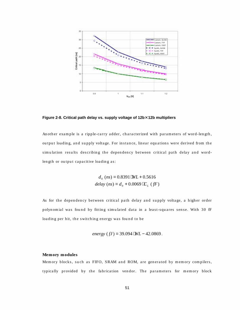
51
Figure 2-8. Critical path delay vs. supply voltage of 12b!!!!12b multipliers
Another example is a ripple-carry adder, characterized with parameters of word-length,
output loading, and supply voltage. For instance, linear equations were derived from the
simulation results describing the dependency between critical path delay and word-
length or output capacitive loading as:
)(0069.0)(5616.08391.0)(
0
0
fFCdnsdelayWLnsd
L⋅+=+⋅=
As for the dependency between critical path delay and supply voltage, a higher order
polynomial was found by fitting simulated data in a least-squares sense. With 30 fF
loading per bit, the switching energy was found to be
0869.42094.39)( −⋅= WLfJenergy .
Memory modules Memory blocks, such as FIFO, SRAM and ROM, are generated by memory compilers,
typically provided by the fabrication vendor. The parameters for memory block
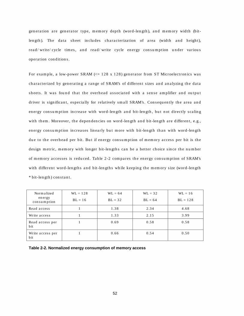
52
generation are generator type, memory depth (word-length), and memory width (bit-
length). The data sheet includes characterization of area (width and height),
read/write/cycle times, and read/write cycle energy consumption under various
operation conditions.
For example, a low-power SRAM (<= 128 x 128) generator from ST Microelectronics was
characterized by generating a range of SRAM’s of different sizes and analyzing the data
sheets. It was found that the overhead associated with a sense amplifier and output
driver is significant, especially for relatively small SRAM’s. Consequently the area and
energy consumption increase with word-length and bit-length, but not directly scaling
with them. Moreover, the dependencies on word-length and bit-length are different, e.g.,
energy consumption increases linearly but more with bit-length than with word-length
due to the overhead per bit. But if energy consumption of memory access per bit is the
design metric, memory with longer bit-lengths can be a better choice since the number
of memory accesses is reduced. Table 2-2 compares the energy consumption of SRAM’s
with different word-lengths and bit-lengths while keeping the memory size (word-length
* bit-length) constant.
Normalized energy
consumption
WL = 128
BL = 16
WL = 64
BL = 32
WL = 32
BL = 64
WL = 16
BL = 128
Read access 1 1.38 2.34 4.68
Write access 1 1.33 2.15 3.99
Read access per bit
1 0.69 0.58 0.58
Write access per bit
1 0.66 0.54 0.50
Table 2-2. Normalized energy consumption of memory access

53
Control The behavior of control modules can be modeled using Stateflow charts, which are
implemented by either generating code onto processor or translating to VHDL and then
being synthesized. An in-house VHDL translating tool was developed [Camera01]. The
goal was to generate a hardware state machine which was as efficient as possible while
remaining functionally equivalent to Stateflow model. Functionality was verified by
cross-simulation of the entire system in Simulink and EPIC TimeMill. The hardware
efficiency was tested by comparing one state machine with hand-coded Verilog
implementation. It was found that the hand-coded version, though significantly less
verbose, was 20% larger in terms of cell area after synthesis.
In a typical digital signal processing system, control logic accounts for less than one-
tenth the power and area of the data-path logic. Consequently, the implementation cost
of the control module is not the dominating factor in making algorithm and architecture
decisions. One approach is to rely on synthesis tools for implementation estimation. Or
high-level estimates can be made based on empirical models [Chadrakasan95], where a
large amount of data from different DSP algorithms was analyzed to develop the model.
Basically the estimates depend on number of states and number of state transitions.
Interconnect One of the difficulties of digital circuit design is timing closure, the process of making
sure that the layout meets the timing constraints assumed in the initial description.
The difficulty arises from the fact that interconnect capacitance is unknown at design
time. Having more accurate pre-layout delay estimates simplifies the problem and
several aspects of this design methodology allow improvement of the estimation
accuracy. First, early specification of the floor plan provides detailed placement
information to the estimation tool. This placement information can be used to estimate
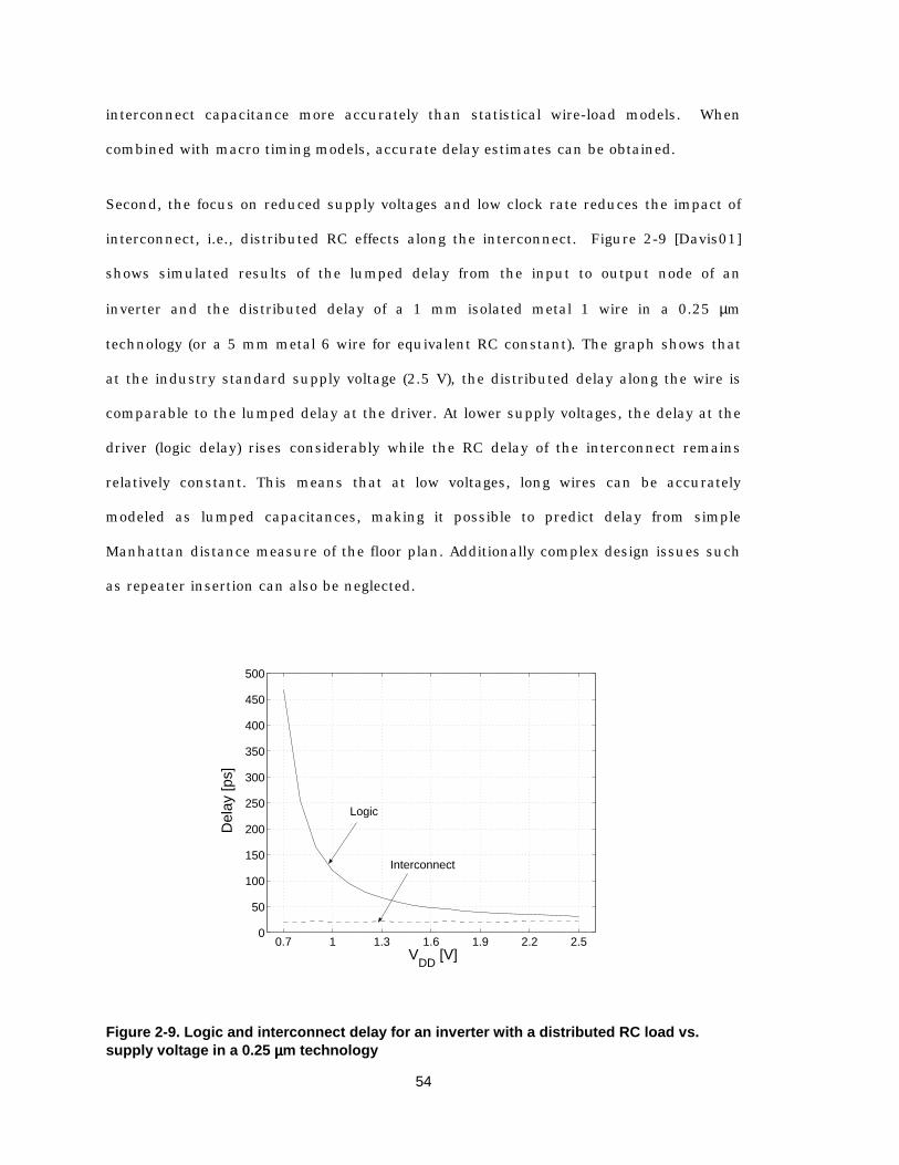
54
interconnect capacitance more accurately than statistical wire-load models. When
combined with macro timing models, accurate delay estimates can be obtained.
Second, the focus on reduced supply voltages and low clock rate reduces the impact of
interconnect, i.e., distributed RC effects along the interconnect. Figure 2-9 [Davis01]
shows simulated results of the lumped delay from the input to output node of an
inverter and the distributed delay of a 1 mm isolated metal 1 wire in a 0.25 µm
technology (or a 5 mm metal 6 wire for equivalent RC constant). The graph shows that
at the industry standard supply voltage (2.5 V), the distributed delay along the wire is
comparable to the lumped delay at the driver. At lower supply voltages, the delay at the
driver (logic delay) rises considerably while the RC delay of the interconnect remains
relatively constant. This means that at low voltages, long wires can be accurately
modeled as lumped capacitances, making it possible to predict delay from simple
Manhattan distance measure of the floor plan. Additionally complex design issues such
as repeater insertion can also be neglected.
0.7 1 1.3 1.6 1.9 2.2 2.50
50
100
150
200
250
300
350
400
450
500
VDD
[V]
Del
ay [p
s]
Interconnect
Logic
Figure 2-9. Logic and interconnect delay for an inverter with a distributed RC load vs. supply voltage in a 0.25 µµµµm technology

55
Third, efforts are made to preserve an algorithm’s locality for architecture design, which
result in dedicated hardware with mostly dedicated, local (short-distance) busses and a
limited number of word level switches (multiplexors). Analytical models for both energy-
consumption and network delay were developed [Zhang99a], which are parameterized
as functions of wire length, switch size, and the number of switches.
2.6.4 Module-based implementation estimation High-level estimates for hardware implementation are needed for evaluation of different
architectural designs to make meaningful decisions. Accurately predicting power and
performance based solely on algorithm and architecture design is a difficult problem. By
taking a pre-characterized library-based approach, a solid base is established for the
estimates. From the cycle-accurate signal flow graph model in Simulink, the block
level connectivity and switching activity information are extracted, together with module
characterization and floor-plan information, energy, area, and critical path delay
estimates are obtained. These estimates can be back annotated to the signal flow graph
so that system designer can get an idea of the cost functions of each sub-system to
make a better trade-off.
Delay First the critical path delay between pipeline registers is identified, which includes both
data-path and control flow. This allows the determination of the lowest supply voltage
(in the range from 0.9 V to 2.5 V for a 0.25 µm technology) with which the design meets
the target throughput requirement, not any faster, and hence minimizes power
consumption. If a fixed supply voltage is used, the critical path delay estimate
corresponds to the fastest cycle time or throughput achievable by that architecture.

56
Block-level linear timing models are used and block connectivity and floor-plan
information are used to determine the loading of each block, which includes the input
capacitance of its driving blocks and wire-loading of Manhattan distance (if available
from physical design information). Special cases are taken into consideration for better
estimation accuracy. For example, the critical path through cascaded adders is much
less than the sum of their individual critical paths. The estimator checks for the special
cases, and applies more accurate delay models rather than worst-case estimates, i.e.,
adding the delays of all the cascaded elements. Future work will focus on a more
accurate method for block-level timing estimates and the use of the floor plan to provide
estimates of wire-load delays.
Energy consumption The total energy dissipation is estimated by a weighted sum of all building components
in the architecture, including arithmetic operations, registers/memory, control and
inter-block interconnect network. The selection of a macro cell library simplifies the
estimation process since the effects of local clock loading and intra-block routing
capacitance are already taken into account during calculation of execution units and
register contribution. For inter-block interconnect, the model from [Zhang99a] is used.
In addition, when connecting blocks are not separated by pipeline registers, a first order
estimation of glitching overhead is added.
A method was also developed to capture switching activity numbers from Simulink
system simulations. An activity monitor for each block can be enabled to record the
number of times the inputs change (i.e., the switching activity), during simulation and
generate a log file. (This slows down simulation considerably.) The activity information
is used together with module energy characterization to determine the weighting factor
of each block and thus achieving more accurate power estimates.

57
Area The total silicon area can be estimated by adding up the area of all required hardware
blocks plus a certain overhead of block level routing and placement, whose value
depends on physical design information. But since the block-level floor plan of the
architecture model is preserved in the design flow, it is easier to get reasonably accurate
estimation.
To verify the approach of this flow, a test chip of decimation filter (containing 307 k
transistors) was fabricated in a 0.25 µm technology [Davis01]. Table 2-3 shows the
performance evaluation of the chip at 1.0 V and 25 MHz. This example showed that the
high-level implementation estimation is fairly accurate, where both delay and power
estimates are within 10% of accuracy compared to post-layout simulation. The area
discrepancy arises from the fact that the hard macros could not be abutted, leading to a
wasted space. This can be avoided with the updated backend design flow.
Signal Flow Graph in Simulink*
Layout** Actual***
Area 2.0 mm2 6.8 mm2 6.8 mm2
Power 16 mW 17 mW 14 mW
Critical Path Delay 19 ns 21 ns in progress
* results from block-level estimation based on cycle-accurate signal flow graph model in Simulink, ** results from post-layout transistor-level simulation using PowerMill and static timing analysis using PathMill, *** measured results on test chip
Table 2-3. Test chip performance comparisons
2.7 Summary
Often different algorithms and architectures are available for the same wireless
communication application, but they achieve quite different system performance and
have quite different complexities that lead to vastly different implementation costs. An

58
exploration methodology is developed, which adopts a top-down approach to design
optimization with bottom-up module-based approach for predictable implementation
estimates. The main feature of such an algorithm/architecture co-design approach is
that it allows for a detailed assessment of key performance measures (e.g., bit error
rate, outage probability, etc.) and implementation parameters (i.e., throughput, area
and power consumption) at an early stage of the design process. Consequently system
designers can explore and evaluate the performance of algorithms as well as their
suitability for highly integrated CMOS implementations.

59
Chapter 3
App l i cat i ons o f Des ign Exp l o rat i on
3.1 Introduction
Wireless communications is one of the fastest growing segments of the high-tech
market and it is also one of the applications that require significant digital signal
processing capability. Future wireless systems are required to provide higher data rates,
improved spectral efficiency and greater capacity to support multimedia applications
and to accommodate the ever-increasing number of users with limited radio spectrum.
This calls for the application of advanced signal processing techniques, which demand
for very high computational throughput. Consequently, it is challenging to implement
solutions capable of real-time operation for high data rate applications at a reasonable
cost in terms of silicon area and with a power consumption that is acceptable for
wireless portable devices.
The successful implementation of advanced algorithms and dedicated hardware
architectures to tackle the demanding signal processing tasks calls for an integrated
development process. It must effectively exploit the many interrelations between the

60
different levels of the design hierarchy and efficiently bridge the gap between system
concepts and their VLSI circuit implementation. That is, in order to exploit the full
potential of recent advances in communication theory and leading edge CMOS
technology, an integrated design framework is required, which allows rapid exploration
of various system realizations, i.e., different performance-versus-complexity trade-offs
at a high level of abstraction. The design exploration methodology presented in Chapter
2 is applied to designs for wireless communications, as an example of DSP systems. To
narrow the focus, algorithms appropriate for an indoor wireless environment are
investigated, where one of the major challenges is to provide enough diversity against
multi-path fading.
Two basic approaches are considered. The first is based on wideband direct-sequence
code-division multiple access (DS-CDMA), which exploits frequency diversity to resolve
the multi-path components at the receiver and uses multi-user detection to suppress
the interference from other users’ signals. The other approach is to employ a
narrowband solution by splitting the channel bandwidth into sub-bands with
bandwidths small compared to the channel coherence bandwidth. The flat fading due to
the destructive addition of the various paths in each of the narrowband can be
combated through exploiting spatial diversity by using multiple antennas at the
transmitter and/or at the receiver. Multi-antenna processing techniques can
additionally be used to increase the capacity. Note although these diversity techniques
have been extensively studied, except for the most elementary techniques, they were
thought to be too complex for implementation in energy and cost constrained portable
devices.
This chapter presents the algorithm and architecture level designs of these two case
studies. A systematic algorithm/architecture exploration approach is demonstrated

61
which leads to efficient implementations in terms of both power consumption and
silicon area.
3.2 Case study 1: multi-user detector for DS-CDMA system
In a DS-CDMA system, as spectral spreading improves the temporal resolution, one
method to achieve diversity is to resolve the multi-path components and hence obtain
several delayed replicas of the same transmitted signal. Four multi-user detection
schemes are evaluated, which can be used in a wideband synchronous DS-CDMA
system [Teuscher98]. A symbol rate of 0.8 M symbols/sec per user with a spreading of
31 for the system yields a chip rate of 25 MHz or a chip period of 40 ns. An indoor
slowly fading environment is assumed which has a Doppler frequency of less than 2 Hz.
With a delay spread of 100 ns, 3-4 multi-path components can be resolved for this
system. All the analyses are based on 28 concurrent users in the system with equal
transmit power, 15 dB signal-to-noise ratio, and 510 − bit-error-rate requirement. Time-
multiplexed pilot symbols are used for channel estimation if necessary.
3.2.1 Algorithms and performance comparisons A brief introduction of the algorithms is given below. The comparison in terms of
computational complexity of the various algorithms is based on the data recovery and
the decision-directed channel tracking parts in the downlink.
Algorithm 1 – Matched filter detection
The received signal over the symbol of interest after the A/D converter is
∑ ∑=
+
α=
K
k jkjjk nsbr
1
rrr
62
where 1ksr is the signature sequence and )1( >jskjr
are its delayed replicas for user k,
jα is the complex channel gain of j-th multi-path, kb is the transmitted signal from
user k, K is the number of active users and nr is the Gaussian noise with covariance
matrix I2σ . The term inside the bracket is defined as the effective signature sequence
for user k, ks~ .
During the pilot period, the effective signature sequence of the desired user is
estimated, say ks , using the RAKE architecture. While in the data period, the
demodulated signal is simply the correlation of the received signal with the estimated
effective signature sequence,
rsb Hkk
rˆˆ =
Because of the interference from other concurrent users, it can only support BPSK to
retain BER performance requirement and hence has a low spectral efficiency. This is a
detection scheme which trades performance for implementation simplicity.
Algorithm 2 – Trained adaptive MMSE detection
The MMSE estimate [Verdu98] of the transmitted signal is
( )( )kHHk rSISSb r~~~ˆ 12 −
σ+=
where [ ]KssS ~~~1 L= .
The update equation for the linear detector in user k is
[ ] [ ] [ ] [ ] [ ]( ) [ ]nrnbnrndndnd kH
kkkrrrrr ∗
−−µ−−= ˆ11
63
and the demodulated signal is
[ ] [ ] [ ]11ˆ +=+ nrndnb Hkk
rr
Algorithm 3 – Blind adaptive MMSE detection
As in Algorithm 1, the effective signature sequence is first estimated, and then in the
data period, the linear detector [Verdu98] in user k is updated as
[ ] [ ] [ ] [ ] [ ] [ ]( )kkkkk ssnrnrndnrndnd ˆˆ,1,1 −−µ−−=
and the demodulated signal is
[ ] [ ] [ ]nrndnb Hkk
rr=ˆ
Both trained and blind adaptive MMSE detection can support QPSK but the former
needs a training sequence that has more stringent design requirements. For example,
the same pilot symbols can be used for all the users in algorithm 3 but different
training sequences have to be used for different users for the algorithm 2 to converge.
Also, depending on the length of spreading, the training sequence usually requires
longer time than the pilot symbols and hence reduces the overall spectral efficiency. On
the other hand, the computational complexity of trained adaptive MMSE is only about
half that of blind adaptive MMSE.
Algorithm 4 – Exact decorrelating detection
The decorrelated [Verdu98] signal is
( )( )kHHk rSSSb r~~~ˆ 1−
=

64
Since equal power among active users is assumed, subspace optimization can be used
to perform the matrix inversion iteratively from the received signals with knowledge on
the effective signature sequence of the desired user only. As the MMSE algorithms,
QPSK can be supported, but since the size of the matrix inversion is up to the number
of active users and the length of spreading codes, the computational complexity is 2 to
3 orders of magnitude higher than that of the MMSE algorithms (Table 3-1). This
demonstrates that evaluation of algorithms in terms of traditional performance metrics
is not enough, power consumption and complexity in implementation should also be
taken into account. It is interesting to estimate the complexity that will be possible for
implementation in the future if Moore’s law for improvement of digital technology
continues as it has in the recent past. With this assumption it will take approximately
15 years before the technology improves to the level that this algorithm can be
implemented with the power and area that algorithm 3 requires today [Zhang99b].
Clearly, further algorithmic optimization is necessary if a single chip solution is
required.
3.2.2 Algorithm property and computational complexity
Signal flow graph models of the algorithms were made in Simulink to evaluate the
system performance as well as extract algorithm properties. For example, Figure 3-1
shows the model of algorithm 3. Some blocks are scalar operations and the rest are
vector operations. The naming conventions are: prefix “c” indicates complex value,
prefix “s” indicates scalar, prefix “v” indicates vector and the number indicates the
vector length. These are used as derivatives. The inherent concurrency (parallelism) of
the algorithm and data dependencies are revealed by the parallel data paths and
communication directions respectively. The sink block of scalar dependency needs to
wait for the source block to finish for correct operation, while the sink block of vector
dependency can start operating when the first element of the vector has been produced

65
by the source block (depending on the implementation). Consequently, these vector-
processing blocks are semi-concurrent. Other algorithm properties can also be
extracted from the block diagram. For instance, locality is related to the fanout of each
output port and number of delays, regularity is related to number of different types of
blocks required, and precision to achieve given performance is indicated by the word-
length of each block. For this example, most data communications are local except for
vectors cv31_data, cv31_s, and cv31_x. The dominant blocks are two concurrent
complex dot products of length 31 and two semi-concurrent complex multiplications,
both with one scalar input. Some algorithm level low-power optimizations can be easily
identified. For example, constant multiplications such as Product 2 and 3 can be
replaced by passing/negation or shift if the parameter “mu” (step size) is chosen
properly. The only control in this model is for the mode of operation, i.e., blind, training,
or decision-directed, which is implemented by a switch.
First order high-level estimates of the power consumption and area to implement the
above algorithms can be obtained simply by counting the number and type of the
arithmetic operations. Additionally the data accesses required to retrieve and store the
operands must be determined. The algorithms being investigated are profiled and a
simplified form of such a breakdown is given in Table 3-1. The relationship of these
operation counts to the resultant area and power strongly depends on the architecture
used for implementation as will be shown in the following sections. In particular the
cost of the data storage and access heavily depends on the memory architecture. Also
included in this table is the basic operation rate metrics defined in Section 2.3 and the
corresponding lower bounds of power consumption in a 0.25 µm technology.

66
Scalar operations
cv31_x
cv31_data
cv31_s
mu
Figure 3-1. Simulink model of multi-user detection algorithm 3
Algorithm 1 Algorithm 2 Algorithm 3 Algorithm 4
Performance with 28 concurrent users (symbol rate of 0.8M symbol/sec per user):
Data rate per user (Mbits/s)
0.8 1.6 1.6 1.6
Spectral efficiency
(bits/s/Hz)
0.9 1.8 1.8 1.8
Computational complexity (operations per sample with 0.8M sample/sec):
MULT 124 248 496 228656
ALU 124 252 502 237708
MEM 248 620 1240 642754
Word-length 8-bit 12-bit 12-bit 16-bit
Structure Complex vector correlation
1. Complex vector operations
2. Block level parallelism: 67%
1. Complex vector operations
2. Block level parallelism: 100%
Operations on complex matrix of
31x31
MBOPS* 3080 6350 12700 5968100
Lower Bound Power (mW)
0.8 2.5 5.0 3150
* MBOPS = million basic operations of given word-length per second, as defined in Section 2.3 (size)
Table 3-1: Performance and computational complexity comparisons of multi-user detection algorithms
Algorithm 1 is the least computational intensive, but in the presence of multi-path
fading and multi-user interference, it has poor performance in terms of spectral
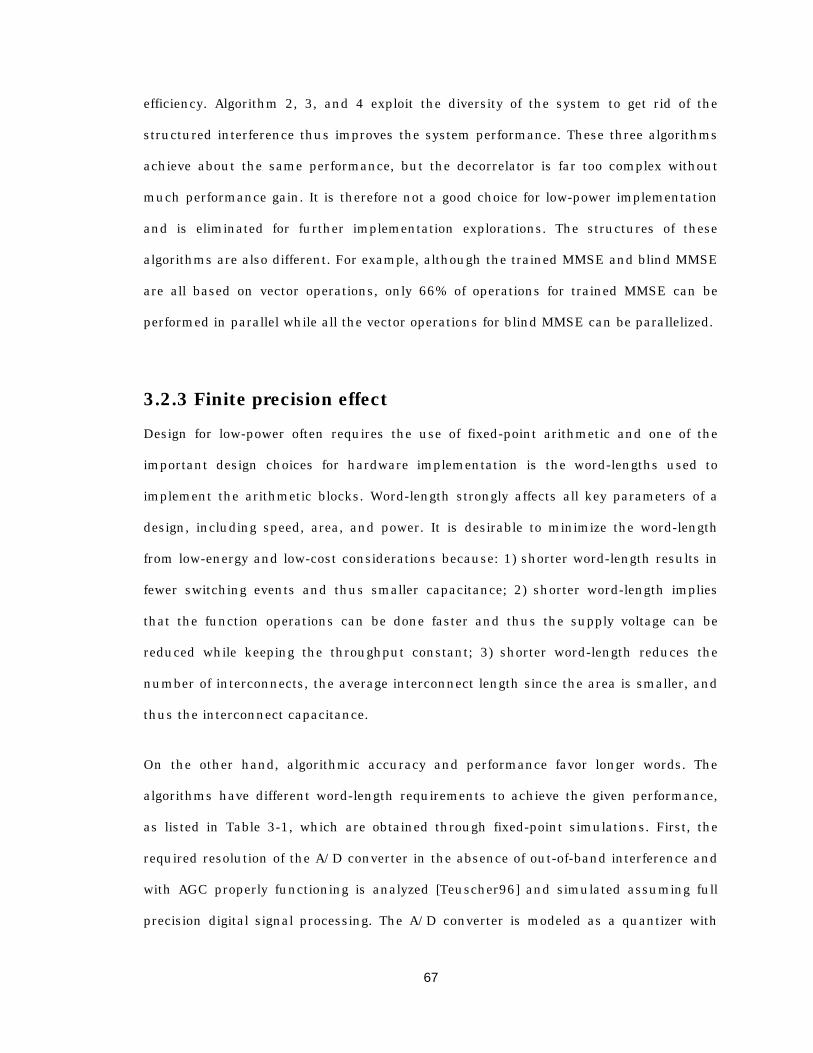
67
efficiency. Algorithm 2, 3, and 4 exploit the diversity of the system to get rid of the
structured interference thus improves the system performance. These three algorithms
achieve about the same performance, but the decorrelator is far too complex without
much performance gain. It is therefore not a good choice for low-power implementation
and is eliminated for further implementation explorations. The structures of these
algorithms are also different. For example, although the trained MMSE and blind MMSE
are all based on vector operations, only 66% of operations for trained MMSE can be
performed in parallel while all the vector operations for blind MMSE can be parallelized.
3.2.3 Finite precision effect Design for low-power often requires the use of fixed-point arithmetic and one of the
important design choices for hardware implementation is the word-lengths used to
implement the arithmetic blocks. Word-length strongly affects all key parameters of a
design, including speed, area, and power. It is desirable to minimize the word-length
from low-energy and low-cost considerations because: 1) shorter word-length results in
fewer switching events and thus smaller capacitance; 2) shorter word-length implies
that the function operations can be done faster and thus the supply voltage can be
reduced while keeping the throughput constant; 3) shorter word-length reduces the
number of interconnects, the average interconnect length since the area is smaller, and
thus the interconnect capacitance.
On the other hand, algorithmic accuracy and performance favor longer words. The
algorithms have different word-length requirements to achieve the given performance,
as listed in Table 3-1, which are obtained through fixed-point simulations. First, the
required resolution of the A/D converter in the absence of out-of-band interference and
with AGC properly functioning is analyzed [Teuscher96] and simulated assuming full
precision digital signal processing. The A/D converter is modeled as a quantizer with
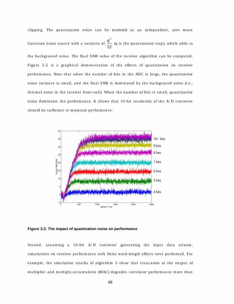
68
clipping. The quantization noise can be modeled as an independent, zero mean
Gaussian noise source with a variance of 12
2q (q is the quantization step), which adds to
the background noise. The final SNR value of the receiver algorithm can be computed.
Figure 3-2 is a graphical demonstration of the effects of quantization on receiver
performance. Note that when the number of bits in the ADC is large, the quantization
noise variance is small, and the final SNR is dominated by the background noise (i.e.,
thermal noise in the receiver front-end). When the number of bits is small, quantization
noise dominates the performance. It shows that 10-bit resolution of the A/D converter
should be sufficient to maintain performance.
4 bits
5 bits
6 bits
7 bits
8 bits
9 bits
10+ bits
Figure 3-2. The impact of quantization noise on performance
Second, assuming a 10-bit A/D converter generating the input data stream,
simulations on receiver performance with finite word-length effects were performed. For
example, the simulation results of algorithm 3 show that truncation at the output of
multiplier and multiply-accumulator (MAC) degrades correlator performance more than
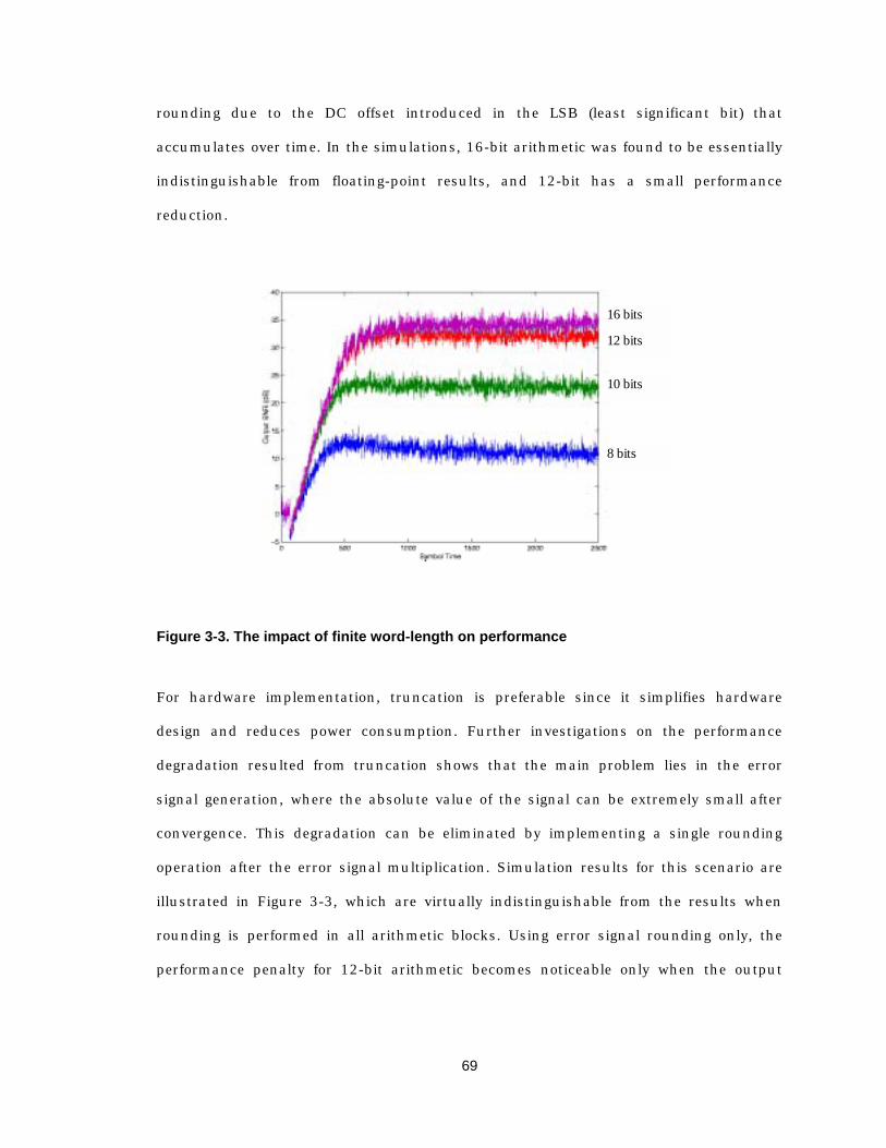
69
rounding due to the DC offset introduced in the LSB (least significant bit) that
accumulates over time. In the simulations, 16-bit arithmetic was found to be essentially
indistinguishable from floating-point results, and 12-bit has a small performance
reduction.
8 bits
10 bits
12 bits
16 bits
Figure 3-3. The impact of finite word-length on performance
For hardware implementation, truncation is preferable since it simplifies hardware
design and reduces power consumption. Further investigations on the performance
degradation resulted from truncation shows that the main problem lies in the error
signal generation, where the absolute value of the signal can be extremely small after
convergence. This degradation can be eliminated by implementing a single rounding
operation after the error signal multiplication. Simulation results for this scenario are
illustrated in Figure 3-3, which are virtually indistinguishable from the results when
rounding is performed in all arithmetic blocks. Using error signal rounding only, the
performance penalty for 12-bit arithmetic becomes noticeable only when the output
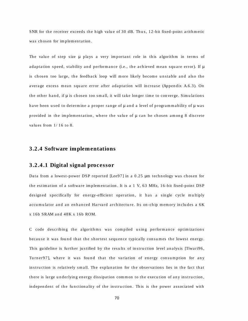
70
SNR for the receiver exceeds the high value of 30 dB. Thus, 12-bit fixed-point arithmetic
was chosen for implementation.
The value of step size µ plays a very important role in this algorithm in terms of
adaptation speed, stability and performance (i.e., the achieved mean square error). If µ
is chosen too large, the feedback loop will more likely become unstable and also the
average excess mean square error after adaptation will increase (Appendix A.6.3). On
the other hand, if µ is chosen too small, it will take longer time to converge. Simulations
have been used to determine a proper range of µ and a level of programmability of µ was
provided in the implementation, where the value of µ can be chosen among 8 discrete
values from 1/16 to 8.
3.2.4 Software implementations
3.2.4.1 Digital signal processor
Data from a lowest-power DSP reported [Lee97] in a 0.25 µm technology was chosen for
the estimation of a software implementation. It is a 1 V, 63 MHz, 16-bit fixed-point DSP
designed specifically for energy-efficient operation, it has a single cycle multiply
accumulator and an enhanced Harvard architecture. Its on-chip memory includes a 6K
x 16b SRAM and 48K x 16b ROM.
C code describing the algorithms was compiled using performance optimizations
because it was found that the shortest sequence typically consumes the lowest energy.
This guideline is further justified by the results of instruction level analysis [Tiwari96,
Turner97], where it was found that the variation of energy consumption for any
instruction is relatively small. The explanation for the observations lies in the fact that
there is large underlying energy dissipation common to the execution of any instruction,
independent of the functionality of the instruction. This is the power associated with
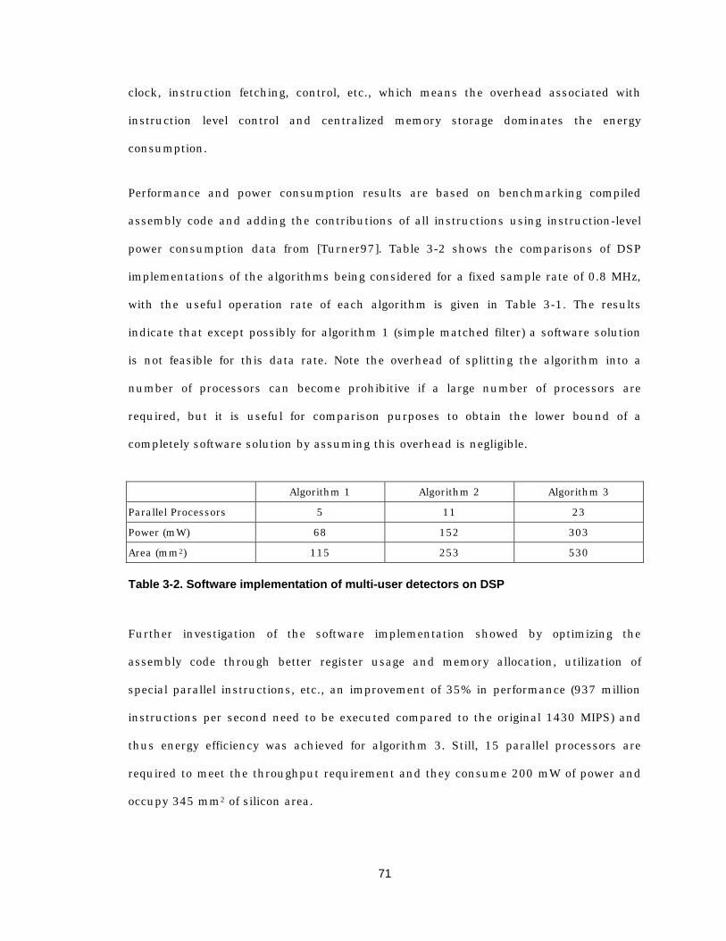
71
clock, instruction fetching, control, etc., which means the overhead associated with
instruction level control and centralized memory storage dominates the energy
consumption.
Performance and power consumption results are based on benchmarking compiled
assembly code and adding the contributions of all instructions using instruction-level
power consumption data from [Turner97]. Table 3-2 shows the comparisons of DSP
implementations of the algorithms being considered for a fixed sample rate of 0.8 MHz,
with the useful operation rate of each algorithm is given in Table 3-1. The results
indicate that except possibly for algorithm 1 (simple matched filter) a software solution
is not feasible for this data rate. Note the overhead of splitting the algorithm into a
number of processors can become prohibitive if a large number of processors are
required, but it is useful for comparison purposes to obtain the lower bound of a
completely software solution by assuming this overhead is negligible.
Algorithm 1 Algorithm 2 Algorithm 3
Parallel Processors 5 11 23
Power (mW) 68 152 303
Area (mm2) 115 253 530
Table 3-2. Software implementation of multi-user detectors on DSP
Further investigation of the software implementation showed by optimizing the
assembly code through better register usage and memory allocation, utilization of
special parallel instructions, etc., an improvement of 35% in performance (937 million
instructions per second need to be executed compared to the original 1430 MIPS) and
thus energy efficiency was achieved for algorithm 3. Still, 15 parallel processors are
required to meet the throughput requirement and they consume 200 mW of power and
occupy 345 mm2 of silicon area.

72
It was found that arithmetic instructions only take about 30-50% of the total execution
time and power, while memory accesses and control take the majority of both. Table 3-3
gives the instruction-wise execution time and power consumption breakdown of
algorithm 3. A hardware component wise breakdown shows that 26% of total power
goes to clocking, 18% to instruction fetching and control, 38% to memory, and 18% to
arithmetic execution. This indicates that considerable improvement can be achieved by
applying low-power design techniques at all levels and from all components. Clocking
power can be reduced by reducing clock loads and switching frequency; instruction
fetching and control power can be reduced by reducing or eliminating number of
instruction fetches and control complexity; memory power can be reduced by reducing
number of memory accesses and memory sizes; and arithmetic execution power can be
reduced by reduction of glitching switches.
Execution Time Power Consumption
Arithmetic instructions 28% 29%
Load/Store instructions 30% 36%
Move instructions 37% 31%
Control instructions 5% 4%
Table 3-3. Execution time and power consumption breakdown for a DSP implementation of multi-user detection algorithm 3
3.2.4.2 General purpose microprocessor Algorithms were also compiled and executed on an ARM8 embedded microprocessor
operating either from a 1 V supply at a clock rate of 40 MHz or from a 3.3 V supply at a
clock rate of 125 MHz. This microprocessor is specifically designed for energy-efficient
operation. Table 3-4 and Table 3-5 give the execution time, power consumption and
their breakdown of the three multi-user detection algorithms. Results are similar to
those obtained for the DSP.
73
Algorithm 1 Algorithm 2 Algorithm 3
40 MHz, 1 V
Parallel Processors 17 35 73
Power (mW) 24 56 112
125 MHz, 3.3 V
Parallel Processors 6 12 23
Power (mW) 264 584 1200
Table 3-4. Software implementation of multi-user detectors on ARM8
Execution Time Power Consumption
Arithmetic instructions 45% 32%
Load/Store instructions 48% 64%
Move instructions 3% 2%
Control instructions 3% 2%
Table 3-5. Execution time and power consumption breakdown for an ARM8 implementation of multi-user detection algorithm 3
It was analyzed in [Burd01] that the hardware overhead required to implement a fully-
programmable microprocessor core increases energy consumption by 30 times above
that required for just the base adder/shifter (which performs computational operations)
and register file circuits (which stores data for the adder/shifter’s operands). Based on
an energy-efficient processor prototype, a factor of 6.4 times increase in energy
consumption is attributed to the additional hardware required to build an ALU and
register bank. This hardware includes latches, muxes, bus drivers, clock drivers, and
associated control circuitry. Additionally, the ALU includes a logic unit, a zero-detect
unit, and a fast 4-bit shifter, while the register bank includes a 5b to 32b register file
decoder for each of its two read ports and one write port. Another factor of 4.7 times is
due to the additional hardware of the processor core, which supports instruction
fetches, branches, branch prediction, loads, stores, and other ISA (instruction set
architecture) specific functionalities. Consequently, this overhead will always dominate
the total processor energy consumption.

74
3.2.4.3 Application specific processor Improvements on software-based implementations can be made through supporting
application-specific instructions and adding accelerating co-processors. It was observed
from the signal flow graph model (Figure 3-1) that the data-path of algorithm 3 operates
on complex numbers, one way to improve efficiency is to modify the data-path to be of
complex ALU and complex MAC and the data memory to be of 32-bit word, 16 bits for
either real or imaginary part. Also, this algorithm does not need all the memory
provided on the DSP, two 256 x 32 bit SRAM banks for data memory and a 256 x 16 bit
SRAM for instruction memory are sufficient (this memory structure already doubles the
requirements of this algorithm). Based on this application-specific processor
architecture (DSP extension), it is estimated that 320 MIPS are required, a reduction of
66% compared to that for the original DSP architecture. The estimated implementation
takes 5 parallel processors, consumes 67 mW of power, and occupies 80 mm2 of silicon
area.
The energy saving comes from reduction of instruction fetching and decoding, reduction
of memory access count and large memory overhead, and optimization of arithmetic
execution units. The main idea behind this approach is that due to the large power
overhead associated with each instruction, packing instructions or adding more
complicated execution units reduces the relative overhead. Also, by operating on
complex numbers this architecture better matches the algorithm. For example, for a
complex multiplication
Y_real = A_real * B_real – A_imag * B_imag;Y_imag = A_real * B_imag + A_imag * B_real;
this architecture only need to read A and B from memory once instead of twice as in the
original DSP architecture.
75
3.2.5 Reconfigurable hardware Pleiades architecture [Wan00] is a domain-specific hardware reconfigurable processor,
which is composed of a programmable, low-energy ARM processor (only used for
configuration) and heterogeneous computing elements, i.e., satellites, of 16-bit word-
length. The architecture reduces instruction fetch and global control overhead by
utilizing distributed control and configuration. It is a reconfigurable computational
engine consisting of spatially programmed connections of satellites, each of which has
its own simplified programmable controller. To map a kernel to an accelerator, the
processor uses the available satellites and the reconfigurable interconnect to compose
the corresponding data flow graph in hardware, dedicated links between satellites are
established to preserve temporal data correlation. The communication mechanism
between each satellite is dataflow driven. Parallel processing is achieved by using
multiple satellites. However, the overheads associated with interconnect, memory and
address generators still exist. Algorithm 3 was mapped onto a Pleiades processor,
resulting in about 24 mW of power from a 1 V supply and 30 mm2 of silicon area in a
0.25 µm technology.
3.2.6 Direct mapped implementations A direct mapped implementation maps each function of the data flow graph of the
algorithm into a dedicated hardware block. For each data flow block, there are several
possible implementations resulting in different latency and throughput for the same
functionality. For instance, the dot product block can be time-multiplexed to a single
two-stage pipelined complex MAC with a counter as local control, with each input being
one element of vector at a time and output being produced every vector length N cycles
(with latency = N +1 cycles). The fully-parallel implementation of this block uses N two-
stage pipelined complex multipliers and log2N complex adders, where all the vector
elements need to be available before executing and the output is produced every cycle
76
(with latency = (2 + log2N) cycles). The selection is based on the design specification and
the trade-off between speed, area, and power consumption.
Figure 3-4 shows the block diagram of an adaptive pilot correlator using algorithm 3
and the corresponding layout view of the dedicated implementation. (Blocks are
separated by pipeline registers and the MAC’s and Mult’s have one pipeline register
internally.) This dedicated design has duplicated functional units with dedicated data
sources and vastly reduced control. It directly matches to the algorithm with a high
level of parallelism and optimization. Algorithm and architecture level low-power design
techniques [Chandrakasan95] were applied. For example, the feedback loop is the
bottleneck in this adaptive algorithm. Adding delays in the loop can relax the critical
path requirement, allowing lower supply voltage. However, the modified algorithm needs
to be analyzed to insure there is no system performance degradation. A DLMS (delayed
LMS) algorithm [Long89] was adopted with D = 2. The direct mapping strategy also
avoids wasteful activity associated with over accurate computation. 12-bit word length
was used in the arithmetic based on fixed-point performance simulations (Section
3.2.3).

77
Conj/Shift
Add
-
S Reg
MAC1
MAC2
X Reg
Add Add Mult2
Mult1 ys
Zm e
cm
-
µo yx ZS
ZX
sm
y
Mult2
Mac2Mult1 Mac1
S reg X reg Add,Sub, Shift
Figure 3-4. Direct mapped implementation of multi-user detection algorithm 3
Energy savings are achieved from all components, where all the low-power design
techniques can be utilized to the greatest extent:
• Clocking: circuits run at lower clock rate resulting in less clock switching per
useful operation; gated clocks are used to “shut down” unused blocks; there is
less clock load due to highly optimized and efficient circuits and smaller
distribution tree due to smaller chip area.
• Instruction fetching and control: totally eliminate instruction fetching and
reduce control to minimum.

78
• Memory: only use optimally sized register files for global vectors without storing
local values that pass through pipeline registers due to the use of dedicated
data-path and communication links, which also avoids the area overhead of
large on-chip memories.
• Bus: use dedicated links to preserve data correlation which can lead up to 30%
energy saving [Turner97] and use the shortest word-length necessary to reduce
wasteful activity.
• Execution units: each algorithmic function has a corresponding dedicated
hardware unit thus providing a high level of optimization of the hardware for a
particular algorithm. In this example, the multiplier and MAC units are the
dominant source of power consumption, any power saving from these units
could lead to noticeable total power reduction. By using 12-bit data-path instead
of 16-bit, a power reduction of about 40% is achieved. Also, the multiplier and
MAC in the module library use a semi-custom carry-save Booth encoded
structure, which does not treat two inputs (A and B) symmetrically, switching in
B, which connects to Booth encoder, consumes more energy. In this algorithm,
the two complex MAC’s have one input (cv31_data) with less correlation than the
other (cv31_s and cv31_x), and the two complex multipliers have one input as
scalar which stays constant while the other input changes 31 times. By
connecting the more correlated signal to B, energy saving of 10-30% can be
achieved [Zhang98a].
A test chip with four adaptive pilot correlators was fabricated in a CMOS 0.25 µm
technology [Zhang98a]. Three different modes of adaptation are implemented: training
sequence based, decision-directed, and blind, with an external control signals
permitting dynamic switch between these three modes of operation. The area and power
dissipation are estimated using the methodology presented in Chapter 2. Table 3-6
compares the hardware implementations of the three algorithms being considered,
where power and area estimates are based on the library modules used for the test
chip. All the implementations operate with a clock rate of 25 MHz from a 1 V supply.

79
Algorithm 1 Algorithm 2 Algorithm 3
Word-length 8 12 12
Complex mac/mult units
1 2 4
Add/sub/shift units 0 6 10
Registers 68 147 225
Power (mW) 0.5 3.9 6.8
Area (mm2) 0.4 1.7 3.1
Table 3-6. Hardware implementation comparisons of multi-user detection algorithms
3.2.7 Architectural implementation comparisons The algorithm/architecture co-design is a two-dimensional design exploration. The
relative implementation costs of various algorithms depend on the architecture choice;
and the relative efficiencies of various architectures depend on the algorithm choice.
Those results can be traced to explicit properties and features of the algorithm and
architecture themselves.
For this case study, there are three algorithms being considered and the
algorithm/architecture design space exploration is illustrated in Figure 3-5. Since
energy consumption is one of the most stringent constraints for portable devices, the
relative energy was used as an example to evaluate the trade-offs. For DSP
implementations, since the three algorithms have similar control flows, their relative
energy consumption directly relates to their operation ratio. The DSP extension has a
complex MAC unit in addition to the DSP, which optimizes the dot product
implementation. Consequently the relative energy consumption also depends on the
operation mix. For dedicated hardware, more algorithm characteristics become relevant,
such as word-length and concurrency. The gains by using dedicated hardware
compared to software implementation also depend on algorithm characteristics. For
example, algorithm 1 (matched filter) has large energy saving since DSP cannot take

80
advantage of its low precision requirement. And more energy savings can be obtained by
using dedicated hardware for algorithm 3 compare to algorithm 2 due to its more
concurrent structure.
1
10
100
1000
Rel
ativ
e En
ergy
pe
r Sa
mpl
e
DSP DSPExtension
DedicatedHardware
Matched FilterTrained MMSE
Blind MMSE
Word Length Concurrency
OperationCount
MAC%
Algorithm Properties
Figure 3-5. Illustration of algorithm/architecture design space exploration
The comparisons of architectural implementations of algorithm 3 are shown in Table 3-
7 and the breakdowns are depicted in Figure 3-6. To make the comparisons fair, same
supply voltage and technology are assumed for all the architectures. For DSP
implementations, since one processor cannot meet the throughput requirement at low
voltage, parallel processors are assumed. (An alternative approach is to raise the supply
voltage so that the processor would run faster but the energy overhead would be
significant due to the quadratic dependency between energy consumption and supply
voltage.) Notice the DSP extension, an application-specific processor (ASP), can achieve
considerable savings in both power consumption and area while retaining the
programming flexibility since it is better matched to the algorithm. A more optimized
architecture is domain-specific reconfigurable hardware (Pleiades), where computation
kernels are mapped to satellite processors. The dedicated hardware achieves the highest
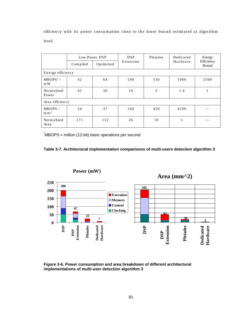
81
efficiency with its power consumption close to the lower bound estimated at algorithm
level.
Low-Power DSP
Compiled Optimized
DSP Extension
Pleiades Dedicated Hardware
Energy Efficiency
Bound
Energy efficiency
MBOPS* / mW
42 64 190 530 1900 2500
Normalized Power
45 30 10 5 1.4 1
Area efficiency
MBOPS / mm2
24 37 160 420 4100 --
Normalized Area
171 112 26 10 1 --
*MBOPS = million (12-bit) basic operations per second
Table 3-7. Architectural implementation comparisons of multi-users detection algorithm 3
Power (mW)
0
50
100
150
200
250
DSP
DSP
Ext
ensio
n
Plei
ades
Ded
icat
edH
ardw
are
ExecutionMemoryControlClocking
Area (mm^2)
DSP
DSP
Ext
ensi
on
Plei
ades
Ded
icat
edH
ardw
are
200
67 23
7
345
83 30 3
Figure 3-6. Power consumption and area breakdown of different architectural implementations of multi-user detection algorithm 3

82
The energy-inefficiency of the software approach is not due to its lack of parallelism.
The optimized software implementation requires at least 15 parallel processors to meet
the throughput requirement. This shows that blindly adding parallel processing
elements without matching to the target computation is not sufficient. The parallel
processor approach only avoids the extra energy overhead associated with voltage
scaling, a factor of about 5x, without fundamentally changing the high degree of time-
multiplexing and flexible structure of DSP. In general, the energy overhead of a DSP is
about 2-3 orders of magnitude compared to dedicated hardware design. This significant
range of difference comes from the following components:
• Execution units: a factor of 6x is attributed to the overhead hardware required
to build a fully programmable ALU and register bank in addition to the basic
computation and storage unit [Burd01]. The dedicated hardware can also use
shortest word-length and preserve data correlation. These application–specific
low-power design techniques save another factor of 2x in energy consumption in
this example [Zhang98a].
• Instruction fetching and control: a factor of 5x is due to hardware support for
instruction-specific functionalities [Burd01]. In the design example, control
circuits consume about the same energy as execution units.
• Memory access: it is a significant source of energy consumption in a DSP due to
its highly time-multiplexed architecture, which requires a large amount of
memory accesses per useful computation. In this design example, 40% of total
energy consumption is from memory. Also, in order to provide flexibility, the
memory is usually over-designed to accommodate different algorithms, which
adds extra overhead since energy per memory access increases with memory
size. It also causes the area overhead of large on-chip memories of a typical
processor. In the example DSP, CPU only occupies about 25% of the area.
Consequently, memory accounts for another factor of 5-10x overhead in energy
consumption for a DSP. For example, a 16x more energy efficient FFT processor
was reported by optimizing memory structure [Baas99].
83
• Other factors: In this design example, 30% of the energy consumption of the
DSP is from fast clocking scheme required by the time-multiplexing scheme.
Due to its large area, global busses and interconnects also contribute to the
overall overhead.
Since the dedicated hardware gives about two orders of magnitude improvements in
energy and area efficiency, it is attractive for low-power and low-cost implementation,
especially for more sophisticated algorithms, where software implementation becomes
not feasible even from computational capability point of view.
3.3 Case study 2: adaptive interference suppression for multi-antenna system
In this case study the design of a generic scheme for adaptive interference suppression
and diversity combining applicable to radio receivers equipped with multiple antennas
is investigated. After explaining the selection of an appropriate algorithm for the
problem, various ways are evaluated to map the necessary computation onto dedicated
VLSI architectures and area and energy estimates are presented.
Wireless communications are mainly affected by three major impairments, namely
multi-path fading, inter-symbol interference, and co-channel / multiple access
interference. All of these detrimental effects can be combated through the use of
adaptive beam-forming techniques, often also referred to as optimum combining in the
context of mobile radio [Godara-I, Godara-II]. The aim of an optimum combiner is to
weight and sum the signals from a number of antenna elements such that the signal of
interest is reinforced and undesired interference (i.e., ISI and MAI) is suppressed,
therefore maximizing the signal-to-interference-plus-noise ratio (SINR) at the combiner
output. This can be interpreted as a process of adaptive beam-forming, where the beam
pattern of an antenna array automatically adapts itself to the current signal
environment, i.e., by pointing its main lobe in the direction of the desired source and

84
steering nulls towards strong interferers. Additionally, a receiver equipped with such an
antenna array can take advantage of space diversity to mitigate multi-path fading, if the
signals received at different array elements are sufficiently uncorrelated.
There exist a vast number of different techniques to govern the adaptive operation that
adjusts the weighting of each antenna signal. To achieve rapid weight adaptation in
time-varying environments with high levels of disturbance recursive least squares (RLS)
based methods are preferred over the class of least mean square (LMS) algorithms, due
to the its superior convergence speed and smaller steady-state error [Haykin96].
An example system performance simulation is shown in Figure 3-7 [Haller00], where an
antenna array with N = 3 elements is used to separate three signals with different power
levels and directions of arrival (SNRin,1 = 30 dB, DOA1 = 5°; SNRin,2 = 20 dB, DOA2 =
−35°; SNRin,3 = 10 dB, DOA3 = 65°), sharing the same carrier frequency through spatial
filtering. Simulations clearly underline the advantages of RLS-based technique in
situations with severe interference where their LMS counterpart fails to deliver
satisfactory performance. The RLS algorithm converges to within 0.5 dB of the
maximum SNR attainable with the optimal MMSE solution in about 10 iterations. And
this is true for all three signals. On the other hand, the LMS algorithm only works
satisfactorily for the strongest signal, and becomes unacceptable for the weakest one.
Even if all three received signals have the same SNR, the convergence is still slower
than the RLS method. Also the residual error of the LMS is bigger. Unfortunately, there
are two major disadvantages associated with the conventional RLS algorithm: its
problematic numerical properties and its large computational complexity. In the
following sections how these critical issues can be resolved by employing numerically
robust mathematical transformations and by making extensive use of parallel
processing are discussed.
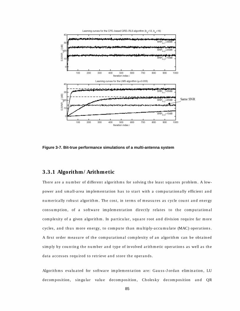
85
Same SNR
Figure 3-7. Bit-true performance simulations of a multi-antenna system
3.3.1 Algorithm/Arithmetic There are a number of different algorithms for solving the least squares problem. A low-
power and small-area implementation has to start with a computationally efficient and
numerically robust algorithm. The cost, in terms of measures as cycle count and energy
consumption, of a software implementation directly relates to the computational
complexity of a given algorithm. In particular, square root and division require far more
cycles, and thus more energy, to compute than multiply-accumulate (MAC) operations.
A first order measure of the computational complexity of an algorithm can be obtained
simply by counting the number and type of involved arithmetic operations as well as the
data accesses required to retrieve and store the operands.
Algorithms evaluated for software implementation are: Gauss-Jordan elimination, LU
decomposition, singular value decomposition, Cholesky decomposition and QR
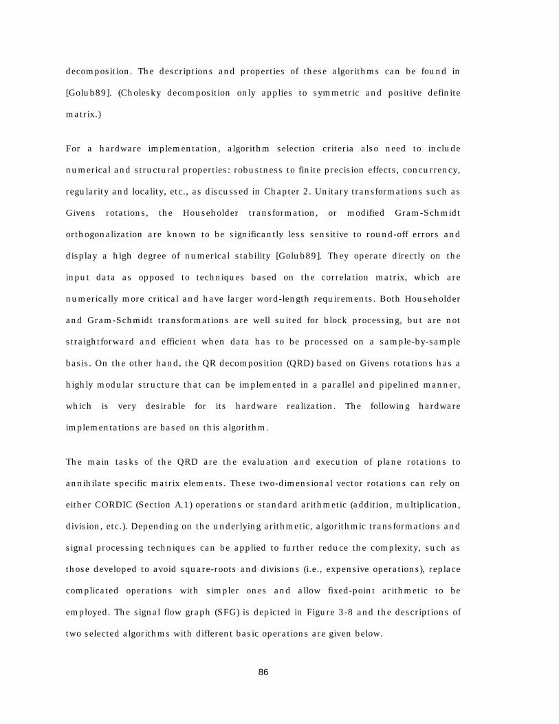
86
decomposition. The descriptions and properties of these algorithms can be found in
[Golub89]. (Cholesky decomposition only applies to symmetric and positive definite
matrix.)
For a hardware implementation, algorithm selection criteria also need to include
numerical and structural properties: robustness to finite precision effects, concurrency,
regularity and locality, etc., as discussed in Chapter 2. Unitary transformations such as
Givens rotations, the Householder transformation, or modified Gram-Schmidt
orthogonalization are known to be significantly less sensitive to round-off errors and
display a high degree of numerical stability [Golub89]. They operate directly on the
input data as opposed to techniques based on the correlation matrix, which are
numerically more critical and have larger word-length requirements. Both Householder
and Gram-Schmidt transformations are well suited for block processing, but are not
straightforward and efficient when data has to be processed on a sample-by-sample
basis. On the other hand, the QR decomposition (QRD) based on Givens rotations has a
highly modular structure that can be implemented in a parallel and pipelined manner,
which is very desirable for its hardware realization. The following hardware
implementations are based on this algorithm.
The main tasks of the QRD are the evaluation and execution of plane rotations to
annihilate specific matrix elements. These two-dimensional vector rotations can rely on
either CORDIC (Section A.1) operations or standard arithmetic (addition, multiplication,
division, etc.). Depending on the underlying arithmetic, algorithmic transformations and
signal processing techniques can be applied to further reduce the complexity, such as
those developed to avoid square-roots and divisions (i.e., expensive operations), replace
complicated operations with simpler ones and allow fixed-point arithmetic to be
employed. The signal flow graph (SFG) is depicted in Figure 3-8 and the descriptions of
two selected algorithms with different basic operations are given below.

87
1,1 1,2 1,3 1,4 1,5
2,2 2,3 2,4 2,5
3,3 3,4 3,5
4,4 4,5
1,6
2,6
3,6
4,6
1,7
2,7
3,7
4,7
1,8
2,8
3,8
4,8
Vec. Rot.
n m
Figure 3-8. Signal flow graph of the QR decomposition algorithm
3.3.1.1 Algorithm 1: Givens rotation based on CORDIC arithmetic
The basic idea underlying the CORDIC based algorithm [Haller00] is to carry out vector
rotations by an arbitrary angle via a series of micro-rotations using a fixed set of
predefined elementary angles, which are chosen such that neither explicit trigonometric
functions nor multiplications are needed. The accuracy of the results depends on the
number of micro-rotation stages and their word-length. The CORDIC has two modes of
operation, which can be implemented using the same hardware cell. Vectoring and
rotation of complex-valued data can be performed by three real CORDIC operations as
depicted in Figure 3-9 [Rader96]. The basic building block of this cell is a micro-rotation
stage consisting of two adder/subtractors and two (right-) shifters. This algorithm is
inherently homogeneous. (Appendix A.2 provides a more detailed description of the
CORDIC algorithm and its implementation.)
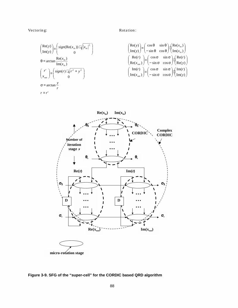
88
Vectoring:
'
arctan
0)('
)Im()Re(
arctan
0))(Re(
)Im()Re(
22
2
rrry
yrrsignxr
xx
xxsignyy
out
in
in
inin
=
=σ
+⋅=
=θ
⋅=
Rotation:
⋅
σσ−σσ
=
⋅
σσ−σσ
=
⋅
θθ−θθ
=
)Im()Im(
cossinsincos
)Im()Im(
)Re()Re(
cossinsincos
)Re()Re(
)Im()Re(
cossinsincos
)Im()Re(
yr
xr
yr
xr
xx
yy
out
out
in
in
Im(r)
Re(xin)
… … …
… … …
… … …
Im(xin)
Number of iteration stage s
θθθθ1111 θθθθ1111
θθθθs θθθθs
σσσσ1111
σσσσs
σσσσ1111
σσσσs
Re(xout) Im(xout)
Re(r)
CORDICComplex CORDIC
D D
micro-rotation stage
Figure 3-9. SFG of the “super-cell” for the CORDIC based QRD algorithm

89
3.3.1.2 Algorithm 2: squared Givens rotation based on standard arithmetic
Squared Givens rotations [Dohler91] are based on standard arithmetic. They offer low
operation count and are square-root operation free. This algorithm requires the
dynamic range of floating-point arithmetic but has reduced word-length requirements
(for the mantissa part) relative to the CORDIC based technique [Lightbody98,
Lightbody99]. Here, the vectoring and rotation operations require different
computations and thus different cells are needed as can be seen in Figure 3-10. The
building elements of the cells are divider, complex multiplier, real multiplier and
adder/subtractor, which can all be decomposed into basic ALU operations. This
algorithm is inherently heterogeneous.
Vectoring:
'
)'
:?0'(
):0?0(
'
2
22
rrrrr
rxrb
xaxrr
ininout
in
inin
=
δ⋅βδ===δ
===
∗δ=δ+⋅β=
Rotation:
rxarrbxx
in
inout
⋅β+∗=
∗−=2

90
RotationRe(b) Im(xin)Re(xin)
Im(a) Re(a)
- δδδδin
Im(b)
Re(xin)
……
Im(xin)
Re(xout) Im(xout)
r
……
…… …
…
… …
… …
… … …
…
… …
Re(b)
δδδδout
Multiplier
Divider
D
D
Vectoring
…… …
… … … …
…
Im(b)
Re(a)
Re(r) Im(r)
…… …
… … … …
…
Im(a)
D D
ALU
Figure 3-10. SFG of the cells for the standard arithmetic based QRD algorithm.
91
3.3.2 Software implementation Since a software implementation provides a large degree of flexibility, it is a desirable
solution if it can meet real-time processing requirements as well as power consumption
and area constraints. TI’s TMS320C6x [TI], a state-of-the-art high performance DSP,
was chosen to evaluate the cost of a software implementation. C6x is a VLIW processor
with 2 independent data paths and 8 execution units. The fixed-point version (’C62) has
a peak performance of 2,400 MIPS (with a 300 MHz clock, consuming 1.6 W of power by
CPU and internal memory), whereas the floating-point version (’C67) delivers up to 1
GFLOPS of computational power.
C code descriptions of the algorithms [Press93] were compiled using performance
optimization and cycle counts were obtained by benchmarking the compiled assembly
code on an evaluation board. Energy consumption was evaluated based on measured
power consumption data of the specific processor [Castille99]. The results for five
different algorithms are summarized in Table 3-8. Assuming computation on a real
matrix of size 4x4, the results indicate that for a software implementation, LU
decomposition is the most efficient algorithm.
Gauss-Jordan
Elimination
LU Decomposition
Singular Value
Decomposition
Cholesky Decomposition
QR Decomposition
Computational complexity (operation breakdown):
SQRT 0 0 25 4 3
DIVISION 4 4 47 14 22
MULT 96 16 455 22 79
ALU 76 10 344 22 79
MEM 376 113 1102 142 309
LOOP 137 127 450 69 142
Cycle count:
TI C6x 11934 9924 46437 10623 19707
Table 3-8. Software implementations of multi-antenna processing
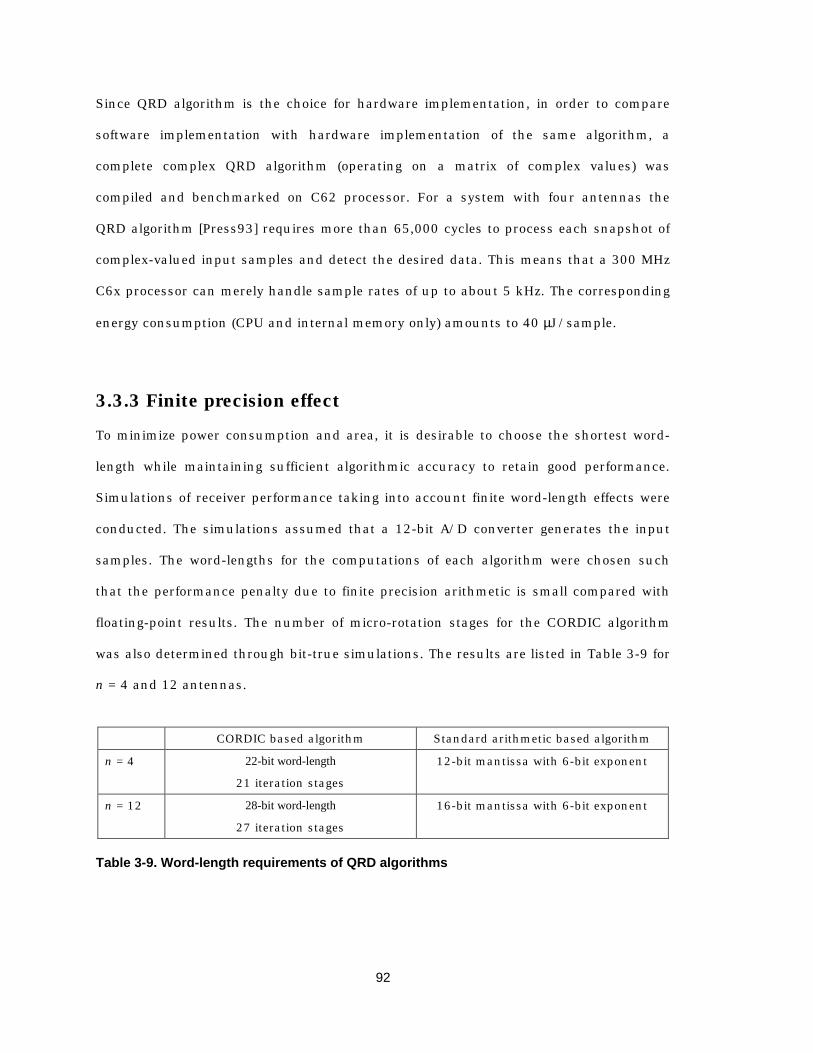
92
Since QRD algorithm is the choice for hardware implementation, in order to compare
software implementation with hardware implementation of the same algorithm, a
complete complex QRD algorithm (operating on a matrix of complex values) was
compiled and benchmarked on C62 processor. For a system with four antennas the
QRD algorithm [Press93] requires more than 65,000 cycles to process each snapshot of
complex-valued input samples and detect the desired data. This means that a 300 MHz
C6x processor can merely handle sample rates of up to about 5 kHz. The corresponding
energy consumption (CPU and internal memory only) amounts to 40 µJ/sample.
3.3.3 Finite precision effect To minimize power consumption and area, it is desirable to choose the shortest word-
length while maintaining sufficient algorithmic accuracy to retain good performance.
Simulations of receiver performance taking into account finite word-length effects were
conducted. The simulations assumed that a 12-bit A/D converter generates the input
samples. The word-lengths for the computations of each algorithm were chosen such
that the performance penalty due to finite precision arithmetic is small compared with
floating-point results. The number of micro-rotation stages for the CORDIC algorithm
was also determined through bit-true simulations. The results are listed in Table 3-9 for
n = 4 and 12 antennas.
CORDIC based algorithm Standard arithmetic based algorithm
n = 4 22-bit word-length
21 iteration stages
12-bit mantissa with 6-bit exponent
n = 12 28-bit word-length
27 iteration stages
16-bit mantissa with 6-bit exponent
Table 3-9. Word-length requirements of QRD algorithms

93
3.3.4 Hardware implementation
3.3.4.1 Architecture space Assume the upper triangular matrix in Figure 3-8 is of size n and there are m additional
columns, which are used to detect multiple simultaneous data streams. Different
architectures are evaluated to implement the signal flow graph, which provide a wide
range of trade-offs between flexibility, area and energy efficiency. A hardware
architecture can be parameterized by the number of parallel processing elements E, the
number of pipeline stages for each element q, the number of basic operations performed
within each pipeline stage p, and the granularity of the processing element G, which is
defined in Table 3-10 for this design example.
CORDIC based algorithm Standard arithmetic based algorithm
Fine granularity
Building element: CORDIC micro-rotation stage
Building element: ALU
Medium granularity
Building element: CORDIC
Building elements: adder/subtractor, real/complex multiplier, divider
Coarse granularity
Building element: complex CORDIC
Building elements: vectoring block and rotation block
Table 3-10. Definition of architectural granularity.
Choosing a larger granularity by grouping the computational elements enables
optimizations within that group, such as using wires instead of shifters (for CORDIC
based algorithm) or using a custom complex multiplier instead of building it from ALU’s
(for standard arithmetic based algorithm). But at the same time, it might decrease the
opportunity for global optimizations as well as reduce the flexibility to map other
algorithms onto the same hardware.
1) 1=E

94
This architecture family resembles an application-specific processor, which has a single
optimized processing unit with a central memory and vastly simplified control. For the
QRD case, since the signal flow is very modular and regular and there are only two
types of operations (vectoring and rotation), control can be achieved by attaching bits to
the data indicating the operation to perform (= 1 bit) and the register file or memory
address from which to fetch inputs (= )2/)1((log2 nnmn ⋅++⋅ bits). In the extreme case
of q = 1 it becomes a purely time-sharing scheme, where the hardware needs to run at a
much higher clock rate than the input sampling frequency, consequently requiring a
high supply voltage which results in increased energy consumption for each operation.
Although this architecture family does not exploit the inherent spatial parallelism of the
two-dimensional SFG, it is possible to exploit temporal concurrency by choosing q > 1.
Also the architecture is flexible in the sense that solutions for matrices of different sizes
can be easily implemented with the same hardware.
2) 2/)1( nnmnE ⋅++⋅=
For this architecture family each node of the algorithm’s SFG is directly mapped onto
silicon. This one-to-one mapping of each algorithmic function onto a corresponding
dedicated hardware unit makes maximum use of the algorithm’s inherent spatial
parallelism. For the QRD case, this approach leads to an upper triangular array
structure where processing elements and memory are all distributed and connected by
dedicated local links and no control is needed. In the extreme case p = max(p) within
each processing element (q has to be 1 due to the recursive loop), i.e., a fully parallel
scheme, the hardware utilization is low and thus it is wasteful in terms of silicon area
without energy saving due to the lower bound of supply voltage. By choosing a smaller
p, time-sharing can be achieved within each processing element. Notice that the total
silicon area grows with E and thus increases quadratically with the matrix size (n and
m).

95
3) 2/)1(1 nnmnE ⋅++⋅<<
Essential to this approach is to map and schedule the two-dimensional signal
processing structure onto a number of parallel processing elements to achieve a high
degree of (i.e., close to 100%) utilization, which leads to the lowest implementation cost
for a fixed throughput. Given any number of parallel processing units, their internal
pipeline schemes and functionality, a program was written to schedule a SFG onto this
processing network to facilitate the exploration of architecture parameter sets. Implicit
to the SFG description is the assumption that there is an infinite time loop surrounding
the computation, which allows the exploration of more temporal concurrency. Multiple
loops are scheduled together through interleaving between input samples for higher
hardware utilization. The communication between processing elements can be achieved
through either a multi-bus or mesh network with dynamic switch [Zhang99a, Benes99].
Communication patterns are recorded from the scheduling scheme and translated to
the switch control.
Scheduling
− Problem statement The control-data flow graph format is used to represent computation, in which nodes
represent operations and edges represent data and control dependencies. A dataflow
graph has a number of nodes N1, N2, …, and a number of edges connecting them, with
the following assumptions:
• The node that the edge points to is the child node and the node the edge
originates from is the parent node. A node may have multiple parents and
multiple children.
• An edge connecting two nodes represents the computation delay between them.

96
• Each node represents a computation load of N processor cycles where N is the
maximum delay between the node and any of its children.
• The dependency of a child node on one of its parent nodes is resolved if the
parent node has been computed for X cycles where X is the computation delay
between them.
• A child node cannot be computed until its dependencies on all its parents are
resolved.
• The graph is not cyclic, i.e. starting from any node traversing the graph through
any of the outgoing edges always ends at a leaf node.
N1 N2 N3
N4 N5
N6
D12 D23
D24 D35
D56
D45
Given a number of processor E1, E2, …, with the following assumptions:
• All the processors are identical and the processors are pipelined with number of
pipeline stage q.
• A computation of load N requires qN cycles to compute ( represents
integer ceil). This is because each processor is assumed to have only one output
port at the end of the pipeline stages so that even if a job does not require q
cycles to compute it will still come out of the processor after q cycles.
• Under the above assumption, the node computation load can be effectively
rewritten as qN instead of N. And the delay on any edge as qD instead of
D.
• The computation of a node needs not to be tied to one processor. A node
requires multiple of q cycles to compute may be computed by different
processors.

97
The task is to find the scheduling of the processors to implement the graph so as to
maximize processor utilization, or equivalently, minimizing the total execution time.
− Algorithm The scheduling algorithm can be described as first available longest path (FALP). To be
specific, every cycle each processor is assigned to compute a node that leads to the
longest path to a leaf. In order to implement the algorithm, a data structure represents
a node will keep the following fields: Number of unresolved parents; Child nodes and
associated delays; Number of children not reached; Number of computation cycles
spent on the node. The following is the scheduling algorithm:
SystemClock = 0;NumNodesFinished = 0;While (NumNodesFinised != total number of nodes)
For each processor If there are nodes marked available for computation
Find the node that has the longest path to a leaf;Assign the node the processor;
else add a bubble to the processor;
SystemClock++;For each processor
Move pipeline forward by one stage;If the retired computation from its pipeline is not a bubble
Find the node the computation is associated with;Update the computation cycle count of the node;For each child node of the parent node
If the edge delay is less than or equal to the computationcycles
(child node).(Number of unresolved parents)--;If ((child node).(Number of unresolved parents) == 0)
Mark child node available;(parent node).(Number of children not reached)--;
If ((parent node).(Number of children not reached) == 0)
NumNodesFinished++;else mark node available;
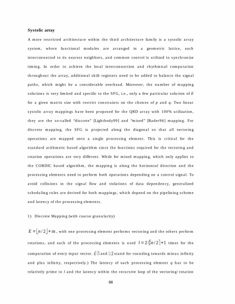
98
Systolic array
A more restricted architecture within the third architecture family is a systolic array
system, where functional modules are arranged in a geometric lattice, each
interconnected to its nearest neighbors, and common control is utilized to synchronize
timing. In order to achieve the local interconnection and rhythmical computation
throughout the array, additional shift registers need to be added to balance the signal
paths, which might be a considerable overhead. Moreover, the number of mapping
solutions is very limited and specific to the SFG, i.e., only a few particular solution of E
for a given matrix size with restrict constraints on the choices of p and q. Two linear
systolic array mappings have been proposed for the QRD array with 100% utilization,
they are the so-called “discrete” [Lightbody99] and “mixed” [Rader96] mapping. For
discrete mapping, the SFG is projected along the diagonal so that all vectoring
operations are mapped onto a single processing element. This is critical for the
standard arithmetic based algorithm since the functions required for the vectoring and
rotation operations are very different. While for mixed mapping, which only applies to
the CORDIC based algorithm, the mapping is along the horizontal direction and the
processing elements need to perform both operations depending on a control signal. To
avoid collisions in the signal flow and violations of data dependency, generalized
scheduling rules are derived for both mappings, which depend on the pipelining scheme
and latency of the processing elements.
1) Discrete Mapping (with coarse granularity)
m2/ += nE , with one processing element performs vectoring and the others perform
rotations, and each of the processing elements is used 12/2 +⋅= nl times for the
computation of every input vector. (⋅ and ⋅ stand for rounding towards minus infinity
and plus infinity, respectively.) The latency of each processing element q has to be
relatively prime to l and the latency within the recursive loop of the vectoring/rotation

99
operation determines the minimum value of l. For the standard arithmetic based
algorithm, the latency to compute a and b in vectoring mode needs to be the same as
the latency of the rotation operation and the latency to compute δ needs to be twice as
much. The mapping and scheduling is depicted in Figure 3-11.
5,5 2,3 1,4 2,2 4,5 1,3 4,4 1,2 3,5 1,1 3,4 2,5 3,3 1,5 2,4 5,5 2,3 1,4 2,2 4,5 1,3 4,4 1,2 3,5 1,1 3,4 2,5
1
Time1,2 1,3 1,4 1,51,1
2,3 2,4 2,5
3,4 3,5
4,5
2,2
3,3
4,4
5,5
3 2
RV vectoring rotation
Mapping Direction
Interleaving of input samples
Figure 3-11. 1D discrete mapping and scheduling of QRD
2) Mixed Mapping (with coarse granularity)
2/nE = , and each of the processing elements is used 1m22/2 +⋅+⋅= nl times for
every input vector. The latency q of each processing element, which is a complex
CORDIC unit (called “super-cell”), has to be set such that lkq ⋅=+12 where k is an
odd integer. Since l is not allowed to be smaller than the latency within the recursive
loop of the vectoring/rotation operation, which is 2/q , there are only two possible
choices of k, namely k = 1 and k = 3. The mapping and scheduling is depicted in Figure
3-12.
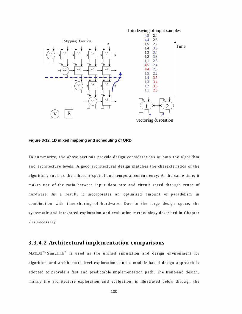
100
1,2 1,3 1,4 1,5
2,3 2,4 2,5
3,4 3,5
4,5
Mapping Direction
1,1
2,2
3,3
4,4
4,5 2,4 4,4 2,3 1,5 2,2 1,4 3,5 1,3 3,4 1,2 3,3 1,1 2,5 4,5 2,4 4,4 2,3 1,5 2,2 1,4 3,5 1,3 3,4 1,2 3,3 1,1 2,5
1 2RV
vectoring & rotation
Time
Interleaving of input samples
Figure 3-12. 1D mixed mapping and scheduling of QRD
To summarize, the above sections provide design considerations at both the algorithm
and architecture levels. A good architectural design matches the characteristics of the
algorithm, such as the inherent spatial and temporal concurrency. At the same time, it
makes use of the ratio between input data rate and circuit speed through reuse of
hardware. As a result, it incorporates an optimized amount of parallelism in
combination with time-sharing of hardware. Due to the large design space, the
systematic and integrated exploration and evaluation methodology described in Chapter
2 is necessary.
3.3.4.2 Architectural implementation comparisons
MATLAB/Simulink is used as the unified simulation and design environment for
algorithm and architecture level explorations and a module-based design approach is
adopted to provide a fast and predictable implementation path. The front-end design,
mainly the architecture exploration and evaluation, is illustrated below through the
101
design example. An adaptive antenna system with n = 12 elements can provide 3 times
the capacity of an n = 4 element system [Godara97a, Godara97b], their corresponding
implementation costs are evaluated in the following and a range of different
architectures for the two systems are compared.
To do this, an integrated set of models were developed: bit-true behavioral models for
system performance simulations, cycle-accurate architecture models with tools for
mapping, scheduling, and architectural implementation estimations with energy-area-
delay models of the parameterized building blocks. Since the SFG is highly regular and
modular, the various schemes in terms of (E, q, p, G) can be searched and the small
number of control signals can be generated in a parameterized manner. The cycle-
accurate architecture models can be automatically generated and subsequently fed into
a back-end design flow to produce a physical layout.
Figure 3-13 depicts the power consumption and silicon area of different architectural
implementations to simultaneously separate and detect n data streams, with the input
sampling rate assumed to be 1 MHz (i.e., n⋅106 complex-valued samples per second).
The results show that different architectures position the design at different points in
the area-energy trade-off space. Notice the results confirm to the simplified model
depicted in Figure 2-2.
The “optimal” point depends on the problem size and design metric, such as area ×
power if they are equally important or area × power2 if energy is of greater importance.
For example, the CORDIC based algorithm with 2/)1( nnmnE ⋅++⋅= , G = 1, q = 1,
and p = 3 gives the best result of area × power2 for n = 4, while the standard arithmetic
based algorithm with discrete systolic array mapping is the best for n = 12, as indicated
by the star in the figure.

102
0 5 10 15 20 250
5
10
15
20
25
30
E=30,G=1,q=1,p=3
Area (mm2)
Pow
er (m
W)
n=4
E=30,G=3,q=3,p=21
E=3,G=1,q=3,p=1
0 50 100 150 200 250 300 3500
50
100
150
200
250
Area (mm2)
Pow
er (m
W)
n=12
E=234,G=1,q=3,p=27
E=32,G=1,q=1,p=9
E=13, G=3, standard arithmetic
Figure 3-13. Hardware implementation comparisons of QRD
Energy per sample estimates can be used as one metric at the system level to trade off
performance and implementation cost. For example, 0.8 nJ/sample for n = 4 and 3
nJ/sample for n = 12 are achieved, obviously more processing energy consumption per
sample is a price to pay for a higher spectral efficiency. Notice that the signal processing
capability offered by dedicated hardware solutions exceeds that of software
103
implementations (1 MHz vs. 5 kHz on DSP) and at the same time dedicated hardware
offers tremendous savings in both energy consumption (0.8 nJ/sample vs. 40
µJ/sample on DSP for n = 4) and area.
3.4 Summary
The realization of a wireless communications system requires optimizations at multiple
levels and demands the designer to think about all design aspects in a unified manner
in order to achieve an efficient real-time implementation of advanced signal processing
algorithms. This chapter applies the algorithm/architecture co-design methodology
presented in Chapter 2 to two case studies of algorithm and architecture level
explorations.
Different architectural implementations are evaluated and compared, which show
several orders of magnitude difference in both energy consumption and silicon area
between software and highly optimized hardware implementations of the same
algorithm. The results are also analyzed to explain the big difference among
architectural implementations. The advantages of considering computational
architecture together with the choice of algorithm is demonstrated, which leads to
efficient implementations.
Since interference suppression techniques can be applied to a wide range of wireless
communications applications to improve system performance, the hardware
implementations presented in this chapter (LMS based adaptive filter for multi-user
detector and adaptive QRD-RLS for multi-antenna processing) can become generic,
high-level, parameterized core blocks. These blocks encapsulate the design knowledge
and facilitate design reuse for component-based system-on-a-chip implementation. By
using these blocks system designers can explore different design parameters and the

104
trade-offs very rapidly and thus allowing them to make early decisions in a more
informed manner. The development of a high-level block library is discussed in
Appendix A, and the library is used in a system design framework presented in Chapter
5.
105
Chapter 4
F lex ib l e A r ch i te c tu res
4.1 Introduction
One characteristic of wireless systems is diverse and evolving application requirements
(e.g., data rate and bit error rate) and changing parameters of the available
communication link (e.g., bandwidth and channel parameters), which directly impact
the choice of system design parameters as discussed in Chapter 5. Consequently it is
desirable for wireless receivers to adapt their operation rather than be only targeted for
a fixed or worst-case scenario. These receivers will have to be flexible enough to
accommodate various operation conditions and their computational requirements while
simultaneously achieving the lowest possible power consumption required for portable
devices. Meeting the combined requirements of high-performance, flexibility, and low-
power consumption is the focus of the architecture design in this chapter.
There is a fundamental trade-off between efficiency and flexibility and as a result, many
programmable designs incur significant energy and performance penalties compared to
fully dedicated specific solutions, a factor which can easily range up to multiple orders
of magnitude. The goal of the function-specific architectures presented in this chapter is
106
to reduce the cost of flexibility in terms of energy and area efficiency, by combining the
system design and an architectural implementation.
The MCMA system, described in Chapter 5, is used as a system design example. After
explaining the desired flexibility at the receiver, various implementations on different
programmable/reconfigurable architectures, ranging from DSP to function-specific
reconfigurable hardware, are evaluated and compared in terms of both energy efficiency
and computation density.
4.2 System requirements for flexibility
A MCMA receiver mainly consists two signal processing parts: OFDM as multi-carrier
processing, with two dominant computational kernel blocks: FFT and Viterbi decoder
[Weste98], and QRD-RLS filter as one possible multi-antenna processing technique
based on MMSE criterion. In addition, timing synchronization is one of the key
functions to ensure proper data recovery in the receiver.
The main parameters of a FFT block are size of transform and input sample rate. The
choice of FFT size depends on the delay spread of the wireless environment, as
explained in Section 5.2.1. Basically: the guard interval needs to be longer than
maximum delay spread, the OFDM symbol duration is chosen to be about 5 times
longer than the guard interval in the interests of transmission efficiency, and the
number of sub-carriers (= FFT size) is determined by (OFDM symbol period – guard
interval) * bandwidth. Since the indoor delay spread is measured in the range from 30
ns to 270 ns depending on the building size [Nee00] and outdoor delay spread is
typically much larger, it is desired to make the FFT size a flexible parameter which can
be set according to the operation environment. The range from 16 to 512 points is
107
sufficient for many wireless applications, with a fixed input sample rate typically limited
either by available bandwidth or A/D converter speed.
The main parameters of a Viterbi decoder are code rate, constraint length, puncturing
rate, survivor path length and decoding rate. Code rate and constraint length directly
relate to coding gain. The lower the code rate (i.e., more redundancy in channel coding)
and the larger the constraint length (i.e., longer memory in channel coding), the larger
the coding gain. Different rates of coding can be constructed by puncturing a base code,
e.g., based on 1/2 rate convolutional code, rate of 2/3 or 3/4 code can be constructed.
Typical constraint length is in the range from 5 to 9. The survivor path length is
typically chosen, depending on constraint length and puncturing rate, to achieve
negligible degradation in performance compared with infinite memory length. With fixed
bandwidth, the decoding rate, i.e., the data rate, depends on modulation scheme and
coding rate. Since different applications have different data rate and BER requirements
and the received SNR can vary significantly depending on the changing wireless
channel, the coding scheme needs to be flexible. Smaller constraint length can be used
to save power for low BER applications since the number of states in a Viterbi decoder
increases exponentially with the constraint length (number of states = 2(constraint length – 1)).
Or puncturing can be used together with higher order modulation schemes, such as 16-
or 64-QAM, for higher spectral efficiency when SNR is high.
Timing synchronization is one of the very first things a receiver has to perform properly
and it is crucial to system performance since in worst case, lost or false detection will
cause the lost of a whole packet. In a PN sequence based timing synchronization
scheme, a sliding-window correlator is the main building block with PN sequence length
as a parameter. The choice of the PN sequence length is a trade-off between
performance and implementation cost: the longer the sequence length the better the
performance at the expense of lower transmission efficiency and higher implementation

108
cost. Since SNR of the received signal for wireless communications has a large range
due to the uncontrollable environmental parameters such as path loss and shadowing
loss, it is desirable to design the correlator to give satisfactory performance even under
the worst-case condition, but not to take the associated overhead under better
conditions. That is to support certain flexibility in the hardware implementation such
that it is able to use shorter PN sequence when SNR is high and to use longer sequence
when SNR is low.
The amount of multi-antenna processing directly relates to the number of transmitting
and receiving antennas. Also, the processing needs to be performed for each
narrowband sub-carriers allocated to a given user, and the number of sub-carriers
depends on the multiple-access scheme. All these parameters may not be fixed at the
design time, consequently it is desirable for the implementation to support a range of
parameter sets.
4.3 Programmable/Reconfigurable architectures
As depicted in Figure 2-1, flexibility in an implementation can be achieved at different
granularities [Rabaey97]. Commonly used programmable or reconfigurable
architectures are categorized in the following sections.
Field-programmable gate array (FPGA) provides reconfigurability at the gate level and
typically uses bit-level mesh network for the interconnect structure, as depicted in
Figure 4-1. Although FPGA’s can exploit the bit-level concurrency to the maximum, for
data-path intensive applications this approach often leads to an energy-inefficient
solution since this architecture implicitly carries an extensive energy overhead and its
reconfiguration granularity is not matched to data-path, which is typically composed of
bus-wide arithmetic modules, such as adders, shifters, registers, etc. Even though
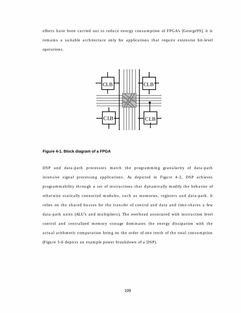
109
efforts have been carried out to reduce energy consumption of FPGA’s [George99], it is
remains a suitable architecture only for applications that require extensive bit-level
operations.
CLB CLB
CLBCLB
Figure 4-1. Block diagram of a FPGA
DSP and data-path processors match the programming granularity of data-path
intensive signal processing applications. As depicted in Figure 4-2, DSP achieves
programmability through a set of instructions that dynamically modify the behavior of
otherwise statically connected modules, such as memories, registers and data-path. It
relies on the shared busses for the transfer of control and data and time-shares a few
data-path units (ALU’s and multipliers). The overhead associated with instruction level
control and centralized memory storage dominates the energy dissipation with the
actual arithmetic computation being on the order of one tenth of the total consumption
(Figure 3-6 depicts an example power breakdown of a DSP).
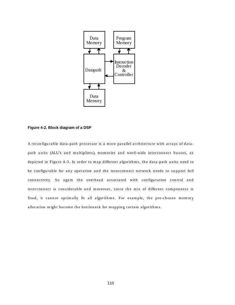
110
DataMemory
InstructionDecoder
&Controller
DataMemory
ProgramMemory
Datapath
Figure 4-2. Block diagram of a DSP
A reconfigurable data-path processor is a more parallel architecture with arrays of data-
path units (ALU’s and multipliers), memories and word-wide interconnect busses, as
depicted in Figure 4-3. In order to map different algorithms, the data-path units need to
be configurable for any operation and the interconnect network needs to support full
connectivity. So again the overhead associated with configuration control and
interconnect is considerable and moreover, since the mix of different components is
fixed, it cannot optimally fit all algorithms. For example, the pre-chosen memory
allocation might become the bottleneck for mapping certain algorithms.
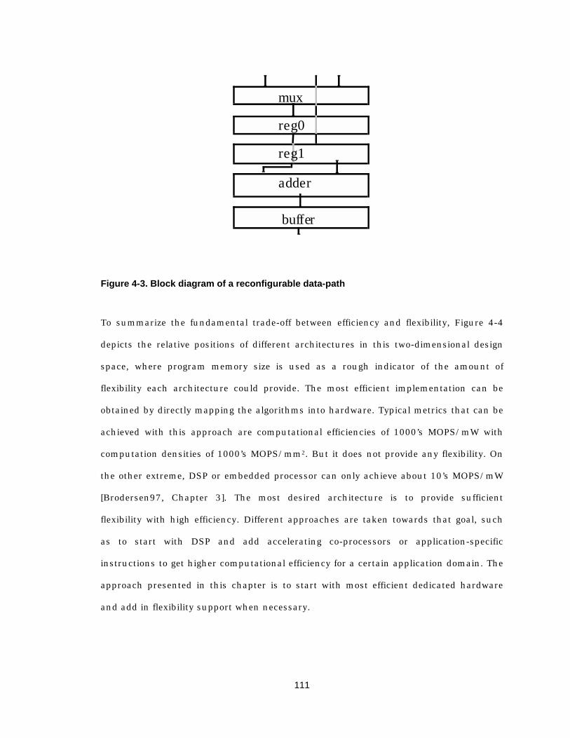
111
adder
buffer
reg0
reg1
mux
Figure 4-3. Block diagram of a reconfigurable data-path
To summarize the fundamental trade-off between efficiency and flexibility, Figure 4-4
depicts the relative positions of different architectures in this two-dimensional design
space, where program memory size is used as a rough indicator of the amount of
flexibility each architecture could provide. The most efficient implementation can be
obtained by directly mapping the algorithms into hardware. Typical metrics that can be
achieved with this approach are computational efficiencies of 1000’s MOPS/mW with
computation densities of 1000’s MOPS/mm2. But it does not provide any flexibility. On
the other extreme, DSP or embedded processor can only achieve about 10’s MOPS/mW
[Brodersen97, Chapter 3]. The most desired architecture is to provide sufficient
flexibility with high efficiency. Different approaches are taken towards that goal, such
as to start with DSP and add accelerating co-processors or application-specific
instructions to get higher computational efficiency for a certain application domain. The
approach presented in this chapter is to start with most efficient dedicated hardware
and add in flexibility support when necessary.
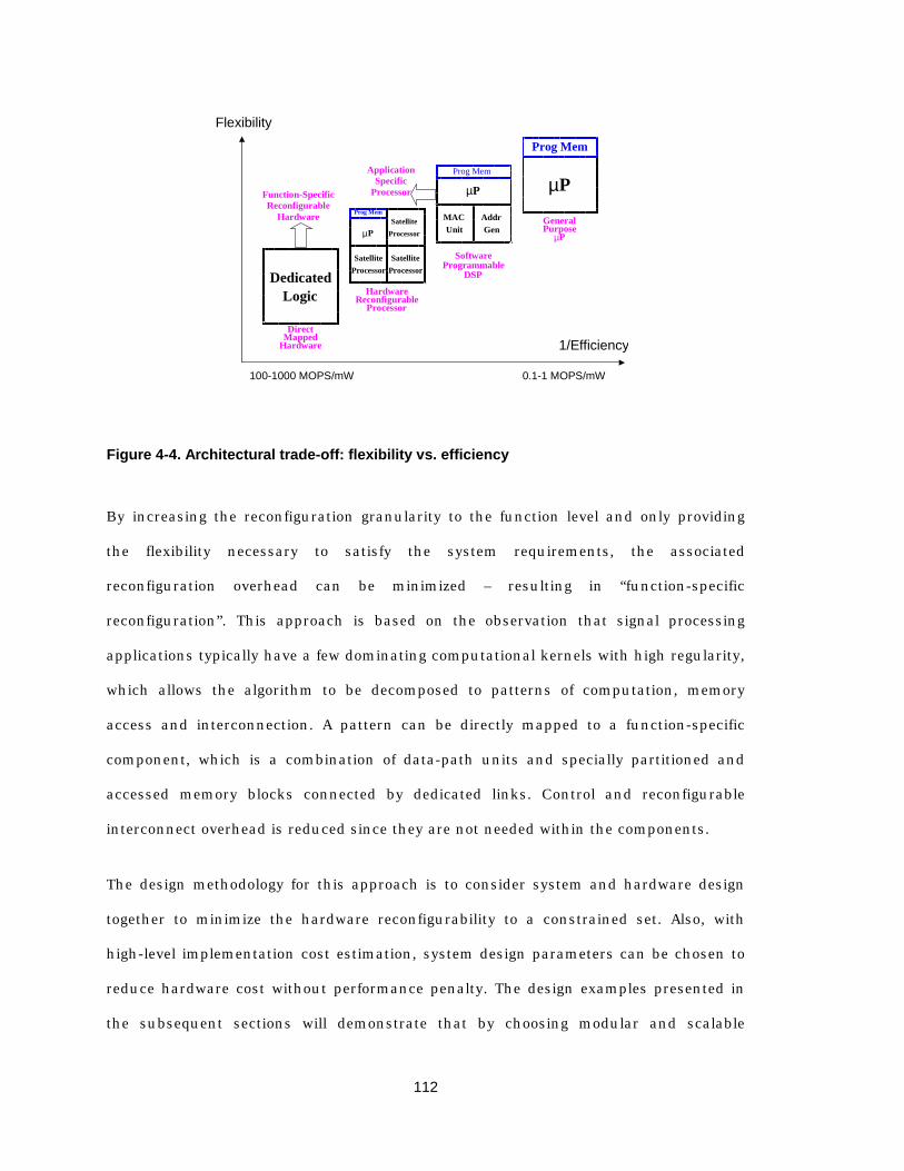
112
µ P
Prog Mem
MAC Unit
Addr Genµ P
Prog Mem
µ P
Prog Mem
Satellite Processor Dedicated
Logic
Satellite Processor
Satellite Processor
General Purpose
µ P
Software
Direct Mapped
Hardware
Hardware Reconfigurable
Processor
Programmable DSP
Flexibility
1/Efficiency
0.1-1 MOPS/mW 100-1000 MOPS/mW
Application Specific
Processor Function-Specific Reconfigurable
Hardware
Figure 4-4. Architectural trade-off: flexibility vs. efficiency
By increasing the reconfiguration granularity to the function level and only providing
the flexibility necessary to satisfy the system requirements, the associated
reconfiguration overhead can be minimized – resulting in “function-specific
reconfiguration”. This approach is based on the observation that signal processing
applications typically have a few dominating computational kernels with high regularity,
which allows the algorithm to be decomposed to patterns of computation, memory
access and interconnection. A pattern can be directly mapped to a function-specific
component, which is a combination of data-path units and specially partitioned and
accessed memory blocks connected by dedicated links. Control and reconfigurable
interconnect overhead is reduced since they are not needed within the components.
The design methodology for this approach is to consider system and hardware design
together to minimize the hardware reconfigurability to a constrained set. Also, with
high-level implementation cost estimation, system design parameters can be chosen to
reduce hardware cost without performance penalty. The design examples presented in
the subsequent sections will demonstrate that by choosing modular and scalable
113
architectures which exploit the algorithm’s inherent structure, sufficient flexibility can
be provided while maintaining high computational efficiency.
4.4 Architecture examples and evaluation methods
To evaluate the energy efficiency of different architectures, the lower bound of energy
consumption for a given technology is estimated as a comparison base. This is
estimated by only counting energy consumption of computation and necessary memory
access, ignoring any control and interconnect overhead. The evaluation methods for all
the architectures being considered are described in the following sections.
Xilinx’s high-performance and high-density Virtex-E family was chosen as an example
of FPGA architecture. The Xilinx CORE Generator system [Xilinx] was used to generate
optimized cores. Performance benchmarks were based on post-layout timing analysis.
Since cores are delivered with logic designs plus optimal floor-plan or layout, the
performance is predictable and repeatable. Energy consumption was estimated by using
an on-line “Virtex Power Estimate Worksheet” [Xilinx]. The effective silicon area was
calculated by (utilization * die area). The die area of XCV300E was estimated to be
about 200 mm2.
Two commonly used fixed-point processors from Texas Instruments were chosen for
this study: the TMS320C6x and the TMS320C5x. The TMS320C6000 platform is an
example of high-performance VLIW DSP, which has two data-paths and eight parallel
processing units as depicted in Figure 4-5, and the TMS320C5000 platform is optimized
for power efficiency. Performance was evaluated based on optimized assembly programs
and benchmarks published by the vendor. Energy consumption, only including CPU
and internal memory dissipation, was estimated based on measured power
consumption data [TI]. The die area of a DSP chip was estimated to be about 50 mm2.

114
C64xTM DSP Core
Data Path 1
D1 ++
Data Path 2
M2 D2 L2
Instruction Decode
Instruction Fetch Control Registers Interrupt
Control
Advanced Emulation
L1 + + + +
S2 + + + +
+ + + +
M1 ++
Instruction Dispatch
Advanced Instruction
Register File A
A31-A16 A15-A0
Register File B
B31-B16
S1 +
+ +
+ x
xxxx
x
x
xx x x
x
B15-B0
Figure 4-5. Block diagram of TI C64x DSP core
Chameleon Systems CS2000 family was chosen as a reconfigurable data-path
processor. It comprises an array of reconfigurable tiles, each contains seven
reconfigurable data-path units, two multipliers, a control logic unit and four blocks of
local store memory, as depicted in Figure 4-6. The tiles are organized in slices with
three tiles per slice. Dynamic interconnect is based on mesh network, which includes
local, intra-slice, and inter-slice connections through multiplexed buses. The
performance and energy consumption results were based on Chameleon Systems
preliminary measurements and estimates [Chameleon]. The power dissipation only from
the reconfiguration fabric was extracted. The die area is about 300 mm2 in a 0.25 µm
technology.

115
Figure 4-6. Block diagram of Chameleon Systems CS2000
Function-specific reconfigurable hardware only adds in necessary configuration to
dedicated design to support the required range of parameters of that function. All low-
power design techniques [Chandrakasan95] used for ASIC designs can be applied. First,
the voltage is chosen for lowest energy-delay product for a given technology (1 V for a
0.25 µm CMOS process technology). Second, a standard-cell module based design
approach is adopted, which facilitates migration to new technology and at the same
time provides predictability of the implementation. After deciding on the building
components of a function, hardware modules are made through synthesis (by Synopsys
Module Compiler, a data-path compiler), placement and route, and their post-layout
area, delay and energy consumption with different levels of loading are characterized.
Also, the modules are designed to have the same width and the pins are placed so that
blocks can be put together in a data-path fashion to ease the inter-block placement and
routing. Memory blocks (i.e., FIFO, SRAM and ROM) are generated by a memory
compiler from ST Microelectronics. The module-based implementation estimation
methodology is described in details in Chapter 2.
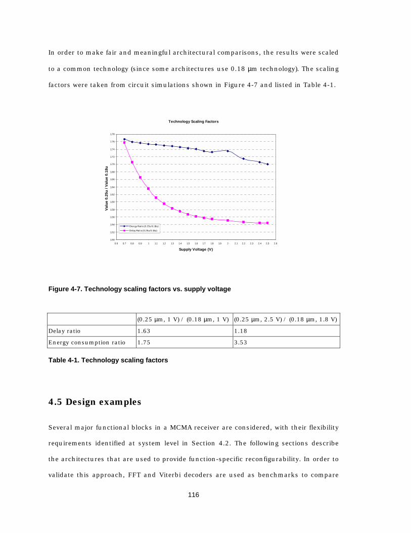
116
In order to make fair and meaningful architectural comparisons, the results were scaled
to a common technology (since some architectures use 0.18 µm technology). The scaling
factors were taken from circuit simulations shown in Figure 4-7 and listed in Table 4-1.
Technology Scaling Factors
1.50
1.52
1.54
1.56
1.58
1.60
1.62
1.64
1.66
1.68
1.70
1.72
1.74
1.76
1.78
0.6 0.7 0.8 0.9 1 1.1 1.2 1.3 1.4 1.5 1.6 1.7 1.8 1.9 2 2.1 2.2 2.3 2.4 2.5 2.6
Supply Voltage (V)
Valu
e 0.
25u
/ Val
ue 0
.18u
Energy Rat io (0.25u/ 0.18u)
Delay Rat io (0.25u/0.18u)
Figure 4-7. Technology scaling factors vs. supply voltage
(0.25 µm, 1 V) / (0.18 µm, 1 V) (0.25 µm, 2.5 V) / (0.18 µm, 1.8 V)
Delay ratio 1.63 1.18
Energy consumption ratio 1.75 3.53
Table 4-1. Technology scaling factors
4.5 Design examples
Several major functional blocks in a MCMA receiver are considered, with their flexibility
requirements identified at system level in Section 4.2. The following sections describe
the architectures that are used to provide function-specific reconfigurability. In order to
validate this approach, FFT and Viterbi decoders are used as benchmarks to compare

117
energy efficiency and computation density to other architectures. Sliding-window
correlator and QRD-RLS filter design are also presented.
4.5.1 FFT To provide function-specific reconfigurability it is first necessary to analyze the
computation structure. The FFT has a shuffle-exchange interconnect structure of
butterfly blocks, which changes with the size of FFT and thus making it difficult to add
flexibility support onto the most energy-efficient fully-parallel implementation (Appendix
A.3.3). However, by choosing a regular pipelined architecture for this algorithm, it is
possible to implement reconfigurable designs with very low energy overhead even
compared with the lower bound.
The radix-22 and radix-23 algorithms [He98] are of particular interest, which have the
same multiplicative complexity as radix-4 and split-radix algorithms respectively while
retaining regular radix-2 butterfly structure. This spatial regularity is a great structural
advantage over other algorithms for VLSI implementation. The basic idea behind the
radix-22 algorithm is to take two stages of the regular DIF FFT algorithm and maximize
the number of trivial multiplications by jW NN −=4/ , which involves only real-imaginary
swapping and sign inversion. In other words, the FFT coefficients are rearranged and
non-trivial multiplications are lumped into one stage so that only one complex
multiplier is needed every two stages. Figure 4-8 illustrates such coefficient
rearrangement: for any two butterfly coefficients iNW and 4/Ni
NW + , iNW is factored out
and put into the next stage, which leaves the coefficients 1 and j− at those positions.
After performing this coefficient rearrangement over all the coefficient pairs, one stage is
left without non-trivial multiplication.
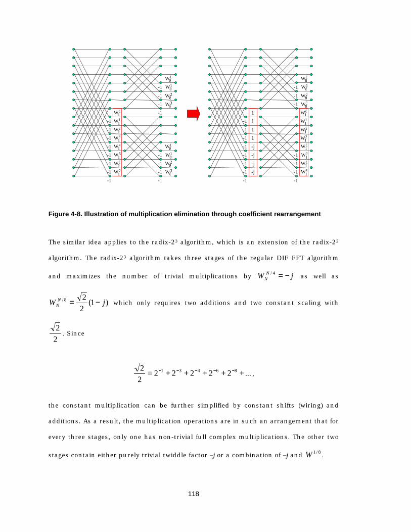
118
01W 11W 21W 31W 41W 51W 61W 71W
08W18W28W38W
08W18W28W38W
-1 -1 -1
-1 -1 -1
-1
-1
-1 -1 -1 -1
-1 -1 -1 -1
08W 18W28W 38W
01W 31W61W 91W
-1 -1 -1
-1 -1 -1
-1
-1
-1 -1 -1
-1 -1 -1 -1
1 1 1 1 -j -j -j -j
01W 11W 21W 31W
Figure 4-8. Illustration of multiplication elimination through coefficient rearrangement
The similar idea applies to the radix-23 algorithm, which is an extension of the radix-22
algorithm. The radix-23 algorithm takes three stages of the regular DIF FFT algorithm
and maximizes the number of trivial multiplications by jW NN −=4/ as well as
)1(228/ jW N
N −= which only requires two additions and two constant scaling with
22
. Since
...2222222 86431 +++++= −−−−− ,
the constant multiplication can be further simplified by constant shifts (wiring) and
additions. As a result, the multiplication operations are in such an arrangement that for
every three stages, only one has non-trivial full complex multiplications. The other two
stages contain either purely trivial twiddle factor –j or a combination of –j and 8/1W .

119
A number of pipelined FFT architectures have been proposed over the last two decades
and they are summarized in Appendix A. Since the spatial regularity of the signal flow
graph is preserved in pipelined architectures, they are highly modular and scalable. The
shuffle network is implemented through a single-path delay feedback depicted in Figure
4-9, where the data is processed between stages in a single path and feedback is used
to store new inputs and intermediate results. The basic idea behind this scheme is to
accept the data in memories and scramble them so that the next stage can receive data
in the correct order. When the FIFO’s are filling with the first half of inputs, the last half
of previous results are shifting out to the next stages. During this time, the operational
elements are bypassing. When the first half of inputs are shifting out of the FIFO’s, they
are fed into the process elements together with the arriving second half of inputs.
During this time, the operational elements are working and generating two outputs, one
directing feeding to the next stages and the other shifting into the FIFO’s. Multipliers
are inserted between stages when necessary according to either the radix-22 or the
radix-23 algorithm.
This simplified interconnect structure makes it easy to achieve flexibility in the length of
the FFT by changing the length of the shift registers (or FIFO’s) and simple multiplexing
the I/O blocks as shown in Figure 4-10. With a clock frequency at the input sample
rate the entire range of FFT’s (from 16 to 512 points) can be accommodated by either
directly mapping to hardware and disabling unneeded blocks for the shorter length
FFT’s or by folding the processing stages and time-sharing the hardware for the longer
(but lower symbol rate) cases. This architecture does not need buffering or serial-to-
parallel conversion.

120
PE3
4FIFO
PE2
2FIFO
PE1
1FIFO
clk
PE3 PE2
PE1 bypass work
work bypass
work work bypass bypass
bypass work bypass work bypass work
Figure 4-9. Illustration of a pipelined implementation of shuffle-exchange interconnect structure
The pipelined scheme for each FFT size is depicted in Figure 4-10 along with the basic
modules. All of them can be mapped onto 6 BF2 blocks shown in Figure 4-11, 2 CM
blocks, 1 ROM (which feeds twiddle factors to the complex multiplier), 1 complex
multiplier and FIFO’s of various sizes. A mapping criterion is chosen to minimize
interconnects which need reconfiguration and maximize dedicated connections. The
resulting design has an area of 1.03 mm2 in a 0.25µm technology.

121
64 128 256
64128
8 4 2 1
N=16 16 8 4 2 1
N=32
16 8 4 2 1 32
N=64 16 8 4 2 1
32 64
N=128
N=256
16 8 4 2 1 32
16 8 4 2 1 32
N=512
N FIFO of length N
CM: Multiplication with )j1(22 −
BF1: Additive radix-2 butterfly
BF2: Additive radix-2 butterfly plus multiplication with -j
Complex multiplier (one input coming from ROM)
Figure 4-10. Pipelined FFT schemes for N=16, … 512
Table 4-2 lists the maximum input sample rate achieved for all FFT lengths with a 1V
supply voltage. (High performance wireless systems, such as IEEE 802.11a, have an
input sample rate of about 20 MHz.) The word-length is up to 12 bits, if less precision is
needed, the lower side bits can be disabled to avoid wasteful switching activity.

122
SelRe Im
Sel1
-
Sel2
BF1
BF2
Figure 4-11. Block diagram of BF1 and BF2
N=512 N=256 N=128 N=64 N=32 N=16
Max. input rate
25 MHz 25 MHz 25 MHz 50 MHz 50 MHz 50 MHz
Power at max. speed
5.1 mW 4.6 mW 4.0 mW 5.5 mW 4.9 mW 4.0 mW
Table 4-2. Implementation parameters of function-specific reconfigurable FFT
The results of the architecture comparison of FFT implementation are shown in Figure
4-12 and 4-13, which demonstrate the tremendous range of efficiencies for various
architectural strategies. In Figure 4-12 the energy required per transform shows that
the most efficient low-power DSP requires more than 2 orders of magnitude more
energy than the lower bound, with the FPGA, reconfigurable data-path architectures
and high-performance VLIW DSP even more inefficient. On the other hand, the
approach that uses function-specific reconfigurability is within a factor of 2-3 of the
lower bound.

123
101 102 10310-10
10-9
10-8
10-7
10-6
10-5
10-4
10-3
Lower limit Function-specific reconfigurable hardwareData-path reconfigurable processor FPGA Low-power DSP High-performance DSP
101 102 103100
101
102
103
104
Lower limit Function-specific reconfigurable hardwareData-path reconfigurable processor FPGA Low-power DSP High-performance DSP
FFT size FFT size
Energy per Transform (J) Million Basic Operations per Second per mW
Figure 4-12. Energy efficiency comparison of FFT implementations
Figure 4-13 presents the area efficiency or computation density, which plots the
performance per unit area. Again the reconfigurable data-path, the various
programmable processors and FPGA and are more than two orders of magnitude less
efficient than the function-specific reconfigurable approach. If a metric is used which
combines both area and energy efficiencies, there is more than 4 orders of magnitude
difference between the most efficient (function-specific reconfigurability) and the other
common digital signal processing solutions.
101 102 103
103
104
105
106
107
108
Function-specific reconfigurable hardwareData-path reconfigurable processor FPGA Low-power DSP High-performance DSP
101 102 103101
102
103
104
105
Function-specific reconfigurable hardwareData-path reconfigurable processor FPGA Low-power DSP High-performance DSP
FFT size FFT size
(Transforms per Second)/(Silicon Area) (Trans/s/mm2) Million Basic Operations per Second per mm2
Figure 4-13. Computation density comparison of FFT implementations
124
The function-specific reconfigurable hardware achieves highest efficiency since it has
the least amount of time-multiplexing and largest granularity among all the designs.
This example suggests that there is a considerable opportunity for adding sufficient
flexibility to application-specific hardware while achieving the energy dissipation near to
the bound provided by the technology.
The conclusion for the cost of flexible granularity is hard to make due to the large
variation of designs from different vendors, even the two DSP’s from the same vendor
show largely different results. Several general observations still can be made. For
example, if compare the data-path reconfigurable processor to high-performance VLIW
DSP in Figure 8, the data-path processor is a more parallel or less time-multiplexed
version with about the same granularity and thus it achieves higher energy efficiency.
Also, Figure 9 shows the least area efficient architecture is FPGA due to its large
overhead with fine granularity of computation. Similar results are obtained for other
designs, such as a Viterbi decoder [Zhang00].
4.5.2 Viterbi Decoder The design of a Viterbi decoder is discussed in Appendix A, it has two main
components: state metric update and survivor path memory.
4.5.2.1 State metric update There is a strong similarity between a shift register process trellis and a FFT signal flow
graph so that architectures for the FFT can be modified and applied to the state metric
update of a Viterbi decoder [Black92a]. A pipelined architecture with single-path delay
feedback was proposed in [Jia99], which utilizes the property of Viterbi algorithm that
the state order returns to natural order after log2N stages of in-place computation. This
means the output can be directly connected to the input without re-circulation. The so-
125
called “supper-pipelined” architecture has M cascaded process elements, each with
log2N ACS units, and thus M*log2N stages are processed in parallel, where N is number
of states.
Based on the pipelined architecture, a parallel-pipelined approach is adopted for the
function-specific implementation, where M processing elements are put in parallel, each
with FIFO lengths 1/M of the original pipelined design, and a shuffle-exchange network
is implemented for the last log2M stages. This approach achieves the same speed-up as
the super-pipelined architecture with reduced memory size and latency (both by a factor
of M). Figure 4-14 depicts the scheme with M = 8 along with the basic modules. This
design can be configured to perform convolutional decoding with N in the range of 16 to
256 (constraint length of 5 to 9), which are typically used for wireless communications
systems. Puncturing can also be supported by inserting erasures in the data stream at
the locations of punctured bits.
Modulo arithmetic is used in the ACS update to avoid normalization [Black92b]. The
required state metric precision is twice the maximum dynamic range of the state
metrics, which is 8 bits for constraint length of 5 to 9 with soft decision inputs of 8
levels. (Appendix A.4.2 provides a detailed discussion of the normalization schemes.)
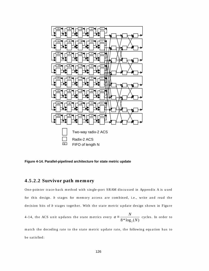
126
16 8 4 2 1
16 8 4 2 1
16 8 4 2 1
16 8 4 2 1
16 8 4 2 1
16 8 4 2 1
16 8 4 2 1
16 8 4 2 1
Two-way radix-2 ACS
FIFO of length NRadix-2 ACS
N
Figure 4-14. Parallel-pipelined architecture for state metric update
4.5.2.2 Survivor path memory One-pointer trace-back method with single-port SRAM discussed in Appendix A is used
for this design. b stages for memory access are combined, i.e., write and read the
decision bits of b stages together. With the state metric update design shown in Figure
4-14, the ACS unit updates the state metrics every )(log*8 2 N
Na = cycles. In order to
match the decoding rate to the state metric update rate, the following equation has to
be satisfied:
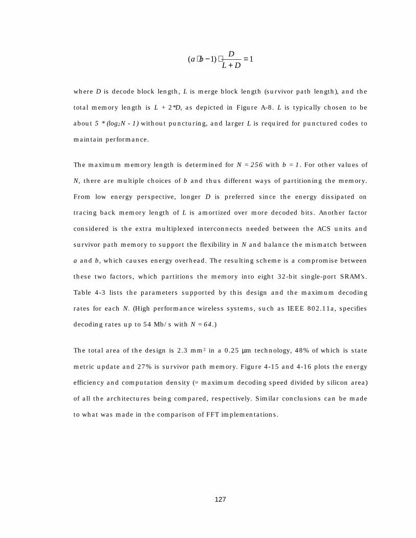
127
1)1( =+
⋅−⋅DL
Dba
where D is decode block length, L is merge block length (survivor path length), and the
total memory length is L + 2*D, as depicted in Figure A-8. L is typically chosen to be
about 5 * (log2N - 1) without puncturing, and larger L is required for punctured codes to
maintain performance.
The maximum memory length is determined for N = 256 with b = 1. For other values of
N, there are multiple choices of b and thus different ways of partitioning the memory.
From low energy perspective, longer D is preferred since the energy dissipated on
tracing back memory length of L is amortized over more decoded bits. Another factor
considered is the extra multiplexed interconnects needed between the ACS units and
survivor path memory to support the flexibility in N and balance the mismatch between
a and b, which causes energy overhead. The resulting scheme is a compromise between
these two factors, which partitions the memory into eight 32-bit single-port SRAM’s.
Table 4-3 lists the parameters supported by this design and the maximum decoding
rates for each N. (High performance wireless systems, such as IEEE 802.11a, specifies
decoding rates up to 54 Mb/s with N = 64.)
The total area of the design is 2.3 mm2 in a 0.25 µm technology, 48% of which is state
metric update and 27% is survivor path memory. Figure 4-15 and 4-16 plots the energy
efficiency and computation density (= maximum decoding speed divided by silicon area)
of all the architectures being compared, respectively. Similar conclusions can be made
to what was made in the comparison of FFT implementations.

128
N=256 N=128 N=64 N=32 N=16
a 4 16/7 4/3 4/5 1/2
b 1 2 2 5 6
D L/2 7L/18 3L/2 5L/2 L
L 48 36,72, 108 2k
k <= 48
6k
k <=16
12k
k <= 16
Max. decoding rate 19 Mb/sec 34 Mb/sec 58 Mb/sec 96 Mb/sec 154 Mb/sec
Power at max. speed
28.6 mW 27.5 mW 22.4 mW 16.7 mW 11.4 mW
Table 4-3. Implementation parameters of function-specific reconfigurable Viterbi decoder
101 10210-11
10-10
10-9
10-8
10-7
10-6
10-5
10-4
Viterbi Decoder States
Ene
rgy
per D
ecod
ed B
it (J
)
Lower limit Function-specific reconfigurable hardwareData-path reconfigurable processor FPGA Low-power DSP High-performance DSP
Figure 4-15. Energy efficiency comparison of Viterbi decoder implementations

129
101 102
104
105
106
107
108
109
1010
Viterbi Decoder States
(Dec
odin
g R
ate)
/(Sili
con
Are
a) (b
/s/m
m2 )
Function-specific reconfigurable hardwareData-path reconfigurable processor FPGA Low-power DSP High-performance DSP
Figure 4-16. Computation density comparison of Viterbi decoder implementations
4.5.3 Sliding-window correlator As discussed in Chapter 5, one major block for timing synchronization (OFDM frame
detection) is sliding-window correlator with PN sequence. Sliding-window correlator is
one of the high-level building blocks presented in Appendix A, where commonly used
low-power design techniques are summarized, such as replacing multiplications with
additions and sign flips and using register file instead of shift registers to reduce
switching activity.
Simulation results show considerable performance gain by using longer PN sequence,
which is necessary to sustain satisfactory performance especially when SNR is low.
However, the implementation costs in terms of area and power consumption, increase
linearly with the length of the PN sequence. Hence there is a trade-off between
performance and implementation complexity. With the effectiveness demonstrated by
the two benchmarks (FFT and Viterbi decoder), the function-specific architecture
approach is adopted. In this example, by considering system design (verifying

130
performance) and hardware implementation together, a compromise can be made which
does not trade in much performance for considerable area and power consumption
reduction. In addition, the proposed solution can switch its operation in response to
better or worse condition with little overhead since most part of the hardware designs
for those two scenarios are common.
A PN code with a hierarchical structure has been proposed in the WCDMA standard to
reduce the computation requirement of the matched filter [3G]. The basic idea is to
construct a 256-chip composite sequence with two 16-chip sequence: a 16 x 16 chip
hierarchical sequence is composed of two length of 16 PN sequences, where the inner
sequence (PN1) is repeated 16 times and each of the 16 copies is in turn multiplied by
an outer 16 chip sequence (PN2). A direct implementation of a matched filter for the
hierarchical sequence only requires 30 (= 2 * (16-1)) complex additions per correlation
output, compared to 255 (= 256-1) complex additions required by a matched filter for a
normal (unstructured) 256-chip PN sequence. This 8-fold reduction of the computation
requirement comes with performance penalty due to the autocorrelation property of
hierarchical sequence not as good as normal PN sequence of the same length.
Five different pilot sequence and their corresponding structures to generate the
correlation metric are illustrated in Figure 4-17 and compared for performance as well
as hardware complexity. Scheme (1) and (5) are normal PN sequences, scheme (1) is a
PN code of length 31 and scheme (5) is a PN code of length 127. The hardware
complexity or implementation cost of scheme (5) is roughly four time that of scheme (1).
Scheme (2), (3) and (4) are based on the idea of hierarchical structured code. They all
have about the same pilot sequence length as scheme (5), but with hardware complexity
about the same as that of scheme (1).

131
Z-1
...
Z-1 Z-1X[n]
PN31(0)
(1)
Pilot sequence: PN31
PN31(1) PN31(30)PN31(29)
Z-1
...
Z-1 Z-1X[n]
PN31(0)
Pilot sequence: [PN31 PN31 PN31 PN31]
PN31(1) PN31(30)PN31(29)
Z-31 Z-31 Z-31
Amptitude ArithmeticMean
Amptitude GeometricMean
Amptitude of sum
Amptitude
(2)
(3)
(4)
Z-1
...
Z-1 Z-1X[n]
(5)
PN127(1) PN127(126)PN127(125)
Amptitude
Pilotsequence: PN127
PN127(0)
Figure 4-17. Sliding-window correlator structures
Figure 4-18 and 4-19 shows the simulated distribution of the normalized correlation
results with SNR = 10 dB and SNR = 1 dB respectively. The farther away apart the two
sets of curves (correlation with random signal or correlation with designed sequence),
the less possible that a lost or false frame detection will occur, thus the better the
performance (Section 5.3.4.2). The results show with SNR of 10 dB, all pairs of the
curves are clearly separated such that a detection threshold can be chosen for each
scheme and satisfactory performance can be achieved.
132
-5 0 5 10 150
0.5
1
1.5
2
2.5
3
3.5PN of length 31 arithmetic mean over 4 PN of length 31geometric mean over 4 PN of length 31 4 PN of length 31 concatenated PN of length 127
Peak to average ratio (dB)
(1)
(2) (3)
(4)
(5)
Correlation with Random Signal
Correlation with Designed Sequence
(1), (2), (3), (4), (5)
Figure 4-18. Simulated timing synchronization performance with different preambles (SNR=10dB)
But when SNR is 1dB, scheme (1) does not give satisfactory results since the pair of
curves have significant portion being overlapped, while schemes (2), (3), and (4) offer
much better performance, close to that achieved by scheme (5). Notice the dominating
part of the correlator implementation is the FIR, which is the same for schemes (1), (2),
(3), and (4), i.e., 31 taps. The extra part of the hardware implementing scheme (2), (3),
or (4) can be disabled for scheme (1). Compared to hardware only implementing scheme
(1), the overhead is very small.
Combining the performance and hardware cost considerations, the hierarchical codes
are better candidates for flexible and low-power implementation as well as achieving
good performance. This example demonstrates the advantage of designing system and
hardware together. Based on the system simulation and together with implementation
estimation, a better trade-off between performance and complexity can be made.

133
-5 0 5 10 150
0.1
0.2
0.3
0.4
0.5
0.6
0.7
0.8
0.9
1PN of length 31 arithmetic mean over 4 PN of length 31geometric mean over 4 PN of length 31 4 PN of length 31 concatenated PN of length 127
Peak to average ratio (dB)
(1)
(2) (3)
(4)
(5) Correlation with Random Signal
Correlation with Designed Sequence
(1), (2), (3), (4), (5)
Figure 4-19. Simulated timing synchronization performance with different preambles (SNR=1dB)
4.5.4 QRD-RLS As described in Chapter 5, QRD-RLS is one possible multi-antenna processing
technique in a MCMA receiver. Depending on system parameters, such as the number
of receiving antenna n, the number of transmitter antennas m (used for concurrent
transmission of independent data stream to a given user), and the number of sub-
carriers k (used for concurrent transmission to a given user), the signal flow graph has
parameters shown in Figure 4-20. Since the processing rate of this block is relatively
slow (~ sample rate / total number of sub-carriers = 20 MHz / 64 ~ 300 kHz in the
design example presented in Chapter 5), time-sharing of hardware can be area efficient
without power consumption overhead. (Supply voltage is lower limited by process
variation considerations and without further supply voltage reduction fully parallel
architecture might not be the lowest power solution even with the cost of a large silicon

134
area. The trade-offs and limits of applying low-power design techniques are provided in
Section 2.5.4.)
n m
.V Ro
…
…
…
…
n m
.V Ro
…
…
…
…
……k
n m
.Vec Rot
…
…
…
…
Figure 4-20. Signal flow graph of parameterized QRD-RLS
The architectural implementation exploration of this QRD-RLS block is a case study
described in Chapter 3, where the goal is to find the most efficient dedicated
implementation for a given problem size (i.e., fixed n, m and k). If a certain degree of
flexibility (i.e., the ability of supporting a range of n, m and k with the same hardware) is
more desired, then the processor network architecture can be used. The scheduling tool
developed for the exploration purpose in Section 3.3.4.1 can be used here for mapping
and scheduling the signal flow graph of any problem set (n, m, k) onto a fixed number of
parallel processing units. Of course, the resulting implementation incurs some
efficiency penalty compared to architecture individually optimized for a given problem
set. The overhead is in the range of a factor of 2 to 5. Consider the order of magnitude
saving in both area and power consumption achieved by adopting hardware approach
rather than software approach and the incapability of software solutions to handle such
amount of computational complexity in real time (Section 3.3.2), the function-specific
design is still significantly more efficient. Once again, this example shows sufficient

135
flexibility support can be added to specially designed hardware that performs a fixed
function efficiently.
4.6 Summary
The combined requirements for high-performance, low-power, and flexibility is the
critical design issue for future wireless digital receivers. In this chapter, a function-
specific architectural approach is proposed to provide the “right” amount of flexibility
identified at system level with minimum implementation overhead. The approach is
evaluated by comparing energy efficiency and computation density to other
programmable or reconfigurable architectures based on different configuration
granularities. Four major processing blocks of an MCMA receiver: FFT, Viterbi decoder,
sliding-window correlator for timing synchronization, and QRD-RLS for multi-antenna
processing, are provided as design examples.
Different architectural designs can provide a wide range of trade-off between energy and
area efficiency and flexibility. Design examples demonstrate that sufficient flexibility can
be provided by a function-specific reconfigurable solution, which offers at least 2 orders
of magnitude higher computation density than can be achieved by FPGA’s, software
processors or reconfigurable data-paths. At the same time, it provides 2 to 3 orders of
magnitude savings in energy consumption. This suggests that there is a considerable
opportunity for adding system required flexibility to application-specific hardware while
achieving area and energy consumption close to the lower bound provided by the
technology. The design strategy is bringing together system, architecture, and circuit
design: identifying the constrained set of required flexibility and computational kernels
at the system level, designing a scalable and modular architecture to exploit the
algorithms’ structures, and applying low-power design techniques.

136
Chapter 5
A MCMA System Des ign F ramework
5.1 Introduction
Chapter 3 and 4 are focused on the design exploration of kernel blocks, this chapter
extends the application of the design methodology to system level. A next-generation
wireless communications system is chosen as a design example of a complex DSP
system, which brings together all the kernel blocks and calls for system-level
optimization by exploring the interaction between signal processing algorithms and
hardware architectures. The example is a multi-carrier and multi-antenna (MCMA)
system.
Wireless system design bears the hindrances of bandwidth limitation and adverse
channel condition as a result of multi-path fading. Over the last two decades,
significant research efforts have dedicated to improve bandwidth efficiency and mitigate
multi-path effects. Techniques to increase wireless system capacity can be categorized
as exploiting time, frequency and/or spatial diversity [Proakis95]. Time diversity is to
distribute the information over a period longer than the channel coherence time.

137
Frequency diversity can be achieved by transmitting over multiple carriers separated by
at least the coherence bandwidth of the channel. Another way to achieve frequency
diversity is through spreading the information content over a large spectrum. As
spectral spreading increases the temporal resolution, more multi-path components can
be resolved and hence the delayed replicas of the transmitted signal can be combined
constructively. Finally, spatial diversity is achieved through the use of multiple
antennas. Theoretical analysis has shown that the mutual information achieved in a
multi-antenna system under flat, independent Rayleigh fading channel grows at least
linearly with the number of transmit or receive antennas whichever is smaller
[Foschini96, Foschini98].
A TFS (time-frequency-space) radio was proposed in [klein00] as a class of next-
generation indoor wireless communications systems which incorporate three key
features: high bandwidth efficiency, resistance to multi-path fading, and multiple-
access capability. The use of multiple antennas is expected to play a key role in fulfilling
these goals. Most multi-antenna processing algorithms are designed for narrowband flat
fading channels. Using multi-carrier processing, the TFS radio effectively divides a
wideband channel into N narrowband channels, facilitating the use of multi-antenna
processing schemes. The MCMA system stems from the concept of TFS radio, with the
goal to build a framework for algorithm and architecture exploration.
5.2 MCMA system fundamentals
An overall block diagram of MCMA system is depicted in Figure 5-1. It mainly consists
of multi-carrier processing and multi-antenna processing, on top of which multiple-
access is supported. The following sections review the fundamentals (algorithms and
problems) of these three components, which are the basis of the system design
framework introduced in the subsequent sections.

138
Transmitter
Receive
Coding and Modulation
Multi-Antenna Processing
(kt)
Multi-CarrierProcessing
(m)
D/A andRF (m)
Multi-PathChannel
RF andA/D (n)
Multi-CarrierProcessing
(n)
Multi-AntennaProcessing
(kr) Demodulation
And Synchro-nization
k carriers, m transmitting antennas, n receiving
Figure 5-1. Block diagram of a MCMA system
5.2.1 Multi-carrier (OFDM) fundamentals OFDM (orthogonal frequency division multiplexing) is one form of multi-carrier
transmission, where a high-rate data stream is split into a number of lower-rate
streams that are transmitted simultaneously over a number of sub-carriers. One of the
main reasons to use OFDM is its robustness against frequency selective fading and
narrowband interference: a single fade or interferer only affects a small percentage of
the sub-carriers and error correction coding can be used to correct the few erroneous
sub-carriers.
A number of parameters need to be designed for an OFDM system, such as the number
of sub-carriers, guard time, symbol duration, sub-carrier spacing, modulation scheme
for each sub-carrier, and the type of forward error correction coding. The choice of
parameters is influenced by system specifications such as available bandwidth,
required data rate, tolerable delay spread, and Doppler frequency. Some requirements
are conflicting. For instance, to get a good delay spread tolerance, a large number of
sub-carriers with a small spacing are desirable, but the opposite is true for a good
tolerance against Doppler spread and phase noise. All these concepts and issues are

139
introduced and discussed in the following sections and at the end a system design
example is given.
5.2.1.1 OFDM signal The complex baseband signal can be written as
TtekUN
nuN
Nk
TtNkj
<≤= ∑−
−=
−π0,)(1)(
12/
2/
)2/(2
where U(k) are the complex modulated data symbols, N is the number of sub-carriers,
with each sub-carrier being t
Nkj
eπ2
, and T is the symbol duration. This complex
baseband signal is of the same form of the inverse Fourier transform of N input data
symbols. The discrete-time equivalent is the inverse discrete Fourier transform (IDFT),
which is given by
2/2/,)(1)(12/
2/
2NnNekU
Nnu
N
Nk
nNkj
<≤−= ∑−
−=
π.
In practice, this transform can be implemented efficiently by IFFT at the transmitter.
Notice that the symbol duration T is an integer-multiple of the period of any sub-carrier,
which accounts for the orthogonality between sub-carriers. At the receiver the data
symbols are retrieved by performing FFT on the received signal, i.e.,
NkNenuN
kUN
Nn
kNnj
<≤−= ∑−
−=
π−2/,)(1)(
12/
2/
2.
The spectrum of OFDM signal is the convolution of impulses located at the sub-carrier
frequencies with the spectrum of a square pulse of period T. The amplitude spectrum of
the square pulse is sinc(πfT), which has zeros at all frequencies that are integer

140
multiples of 1/T. Although the sinc spectrum of individual sub-carrier overlaps, at the
peak of each sub-carrier spectrum, all other sub-carriers have nulls. The receiver uses
the spectrum values only at those peak points, consequently it can demodulate each
sub-carrier free of any inter-carrier interference (ICI).
By dividing the input data streams into N sub-carriers, the symbol duration is made N
times longer, which also reduces the relative amount of dispersion in time caused by
multi-path delay spread. To eliminate inter-symbol interference (ISI), a guard time is
introduced in every OFDM symbol. The guard time is chosen to be longer than the
expected worst-case delay spread of the target operation environment, such that multi-
path components from one symbol will not interfere with the next symbol. To avoid ICI,
the OFDM symbol is cyclically extended in the guard time. As a result, as long as the
multi-path delays are within the guard time, no ISI and ICI will be introduced.
Figure 5-2 illustrates the use of cyclic prefix. At the receiver, the starting time to sample
an OFDM symbol xT needs to satisfy the criterion:
gx TT <<τ∆
where τ∆ is the longest multi-path delay. As long as the above condition is satisfied,
there is no ISI since the previous symbol will only have effect over samples within
],0[ τ∆ . Also by starting sampling from xT all samples will encompass the
contributions from all the multi-path components, i.e., they experience the same
channel, and therefore there is no ICI.

141
gT T
τ∆
Multi-path component A
Multi-path component B
Multi-path component C
xT Sampling period T
Guard time
Figure 5-2. Illustration of cyclic extension
5.2.1.2 Coherent and differential detection In order to demodulate symbols at the receiver, the reference phase and amplitude of
the constellation need to be known. In general, the constellation of each sub-carrier has
a phase shift and amplitude change, caused by carrier frequency offsets, timing offset,
and frequency selective fading. There are two different approaches to deal with these
unknown variations: coherent and differential detection. In coherent detection, the
constellation reference is estimated through training to determine the best decision
boundaries for each sub-carrier, i.e., frequency, phase offset and channel estimations
are required. Differential detection does not use absolute reference, but only looks at
the phase and/or amplitude difference between successive symbols.
A main task of coherent detection is channel estimation. In general, radio channel is
fading in both time and frequency. So a channel estimator has to estimate the time-
varying amplitude and phase of all sub-carriers. There are two kinds of techniques to do
this by using either pilot channels or training symbols.
142
• Pilot channel based techniques: interpolate the channel estimates in both time
and frequency domain based on a few known pilot sub-carriers. This type of
techniques is especially suitable for continuous transmission systems such as
digital audio/video broadcasting. The pilot spacing has to fulfill the Nyquist
sampling theorem, i.e., the requirements for the pilot spacing in time ts and
frequency fs are:
spreaddelays
spreadDopplers ft
1,1 << .
This two-dimensional interpolation can also be separated into two one-
dimensional interpolations.
• Training symbol based techniques: use preamble to estimate the channel
response of all sub-carriers and assume constant channel during the entire
transmission. This type of techniques applies to packet-based communications
such as wireless LAN (local area network). It puts the best effort at the beginning
of every packet to estimate channel to avoid delay in detection and eliminates
the time-varying estimation that is unnecessary if packet length is short enough.
One variation of this method is after at least one known OFDM symbol, start the
decision-directed channel estimation. The first known symbol enables the
receiver to attain channel estimates for all sub-carriers, which are then used to
detect the data in the following symbol. Once data estimates are available, they
are used to remove the data modulation from the sub-carriers, after which all
sub-carriers can be used to further estimate channel or track the slowly time-
varying channel.
The choice of pilot channel density or the number of training symbols is a trade-off
between channel estimation accuracy and transmission efficiency.
In an OFDM system (without multi-antenna processing), only a single tap equalizer (i.e.,
phase correction) is needed for coherent detection after obtaining the knowledge of
channel. Weak sub-carriers (i.e., sub-carriers with smaller amplitude gain through the
channel) get a low weight in the decoding, rather than being extra amplified to equalize
the channel. In this way, an OFDM system can avoid the problem of noise enhancement

143
that is present in linear equalization techniques. Mathematically, after FFT
demodulation, the signal can be represented as
)()()()( kZkXkCkY +=
where C is channel estimate, X is transmitted signal and Z is noise. The decoder
searches for the sequence of )(ˆ kX , which minimizes
∑∑
+−=−
kkkXkCkXkCkYkXkCkY
2**2)(ˆ)()(ˆ)()(Re2)(ˆ)()( .
This (sub-optimal) maximum-likelihood sequence estimation (MLSE) provides protection
against narrow-band deep fading, i.e., unreliable data received at a few weak sub-
carriers. (It is sub-optimal when X(k) is not an independent stream.)
Differential detection does not need any channel estimation and thus reducing receiver
complexity and saving pilot at the cost of degraded performance. This technique can be
applied in either time or frequency domain. In time domain, each sub-carrier is
compared with the same sub-carrier of the previous OFDM symbol. This method relies
on the assumption that the channel is relatively constant over time, i.e., the change in
channel response between two consecutive OFDM symbols is negligible. The SNR after
differential detection is approximately 3 dB worse than the input SNR [Proakis95],
which is the worst case SNR loss of differential detection compared to coherent
detection. In practice, coherent detection also has an SNR loss due to the imperfect
channel estimates, which typically reduces the difference between differential and
coherent detection to about 1-2 dB. For differential detection in frequency domain, each
sub-carrier is compared with the adjacent sub-carrier within the same OFDM symbol.
This method assumes that there is a negligible phase and amplitude difference between
two adjacent sub-carriers. The performance degradation of this method depends on
144
delay spread values and modulation schemes. Larger delay spread (= narrower coherent
bandwidth) means bigger phase and amplitude changes across sub-carriers and thus
differential detection has more impact on the performance, and higher order modulation
schemes are more sensitive to phase errors.
5.2.1.3 OFDM system design example The choice of OFDM parameters is a trade-off between various, often conflicting
requirements. Start with delay spread, as a rule of thumb, the guard time is chosen to
be about 2-4 times the root-mean-squared delay spread [Nee00]. This value depends on
the type of coding and QAM modulation. Higher order QAM (e.g., 64-QAM) is more
sensitive to ICI and ISI, while coding can reduce the sensitivity to those interferences.
For example, if the target tolerable delay spread of an indoor environment is 200 ns,
800 ns is a safe value for the guard time.
Now that the guard time is set, the symbol duration can be fixed. To maximize the
transmission efficiency, it is desirable to have the symbol duration much longer than
the guard time that dose not carry useful information and thus wasting transmission
power. However, longer symbol duration means more sub-carriers with a smaller
spacing, which causes the system to be more sensitive to phase noise and frequency
offset, as well as an increased peak-to-average power ratio. A practical design choice is
to make the symbol duration about 5 times the guard time, corresponding to about 80%
transmission efficiency. For the example, the OFDM symbol duration can be chosen to
be 5 * 800 ns = 4 µs. The sub-carrier spacing is the inverse of 4 µs – 0.8 µs = 3.2 µs,
which is 312.5 kHz. The assumption that each sub-carrier is a narrowband with flat
fading is valid for this design since the coherence bandwidth of an indoor channel is
about the inverse of the delay spread, which is 1/200 ns = 5 MHz in this example and it
is significantly wider than the sub-carrier bandwidth.
145
The number of sub-carriers can be determined if the sample rate (= digital processing
rate and minimum speed of A/D converter) is given, for example 20 MHz. Here it is
required that there must be an integer number of samples both within the FFT/IFFT
interval and in the symbol interval. For the design example, it results in (20 MHz * 3.2
µs = 64) sub-carriers (i.e., 64-point FFT/IFFT) and (20 MHz * 0.8 µs = 16) samples of
cyclic prefix.
Typically, not all the sub-carriers carry data. Some are used for pilot if pilot sub-
carriers are used to assist coherent detection. Some are left empty intentionally, for
example, a few bins at DC. The reason is in a wideband CMOS radio, large low-
frequency flicker noise makes bins around DC prone to error. Also, a few bins at both
frequency edges may be left empty to better handle the aliasing introduced by over-
sampling (e.g., in the D/A converter) and to provide a guard band between adjacent
channels.
5.2.1.4 Issues with OFDM system
Synchronization
Synchronization in an OFDM system includes timing and frequency/phase
synchronization. Timing synchronization needs to find the OFDM symbol boundary and
the optimal sampling point to minimize the effects of ISI and ICI. OFDM scheme is
relatively insensitive to timing offset, but any timing-error can reduce the receiver’s
robustness to delay spread. Since the sub-carriers are perfectly orthogonal only if
transmitter and receiver use exactly the same frequency, any frequency offset results in
ICI. Frequency synchronization needs to estimate and correct the carrier frequency
offset of the received signal. For coherent detection, the phase also needs to be
synchronized. A related problem is phase noise: a practical oscillator produces a carrier
that has a random phase jitter (i.e., the frequency is never perfectly constant), which
146
also causes ICI in the receiver. OFDM is more susceptible to frequency offset and phase
noise, compared to a single carrier system where frequency offset and phase noise only
cause degradation in the received SNR rather than introducing interference. Different
synchronization techniques, by using either cyclic prefix or special training symbols,
can be applied, which are discussed in Section 5.3.4.
Peak-to-average power ratio
OFDM signal consists of a number of independently modulated sub-carriers, which can
give a large peak-to-average power (PAP) ratio since when N signals are added with the
same phase, they produce a peak power that is N times the average power. A large PAP
ratio has disadvantages such as large dynamic range requirement of the A/D and D/A
converter and reduced efficiency of the RF power amplifier, which often dominates the
total power consumption of a transceiver. To reduce the PAP ratio, several techniques
have been proposed, which basically can be divided into three categories [Nee00]:
• Signal distortion techniques: reduce the peak amplitudes simply by nonlinearly
distorting the OFDM signal at or around the peaks. Example techniques are
clipping, peak windowing, and peak cancellation.
• Coding techniques: use a special forward-error correcting code set that excludes
OFDM symbols with a large peak power.
• Scrambling: scramble each OFDM symbol with different scrambling sequences
and select the sequence that gives the smallest PAP ratio.
5.2.2 Multi-antenna fundamentals The quest for ever better usage of the limited radio spectrum, i.e., higher spectral
efficiency in the unit of bits/s/Hz, has fostered great interest in multi-antenna
technology. Multi-antennas systems are employed as an interference suppression
technique as well as a means to mitigate fading by exploiting spatial diversity. That is to

147
say the essence of multi-antenna processing is interference suppression in combination
with diversity combining.
Antenna arrays have been used to increase receive or transmit diversity order against
multi-path fading or spatially separate mobile devices. It was shown that in a richly
scattering channel, signal even from closely spaced transmit antennas can be separated
using adaptive array combining techniques at the receiver. The number of transmit
signals that can be separated grows with the number of receiver antennas [Foschini96,
Foschini98]. Consequently, the use of multiple antennas at both transmitter and
receiver could increase the degrees of freedom in information transmission, with
capacity scaling at least linearly with the number of transmitter or receive antennas,
whichever is smaller.
There are various multi-antenna processing algorithms, the most famous one is V-
BLAST (vertical Bell Laboratories Layered Space-Time) algorithm [Wolniansky98]. V-
BLAST is a combination of zero-forcing nulling and successive cancellation with optimal
ordering. It was demonstrated that a system with 8 transmitting and 12 receiving
antennas achieves a spectral efficiency of 20-40 bits/s/Hz at average SNR ranging from
24-34 dB. The following sections describe other two possible multi-antenna algorithms.
5.2.2.1 MMSE algorithm The aim of a smart antenna is to reinforce the signal of interest while suppressing the
undesired inter-symbol and co-channel interference, which are due to multi-path
propagation and other concurrent transmissions, respectively [Godara97a, Godara97b].
Consequently, a smart antenna maximizes the signal-to-interference-plus-noise ration
at its output. This can be interpreted as a process of adaptive beam-forming where the
radiation pattern of the antenna array is automatically adjusted accordingly to the
signal propagation environment, i.e., by steering the main lobe towards the signal of
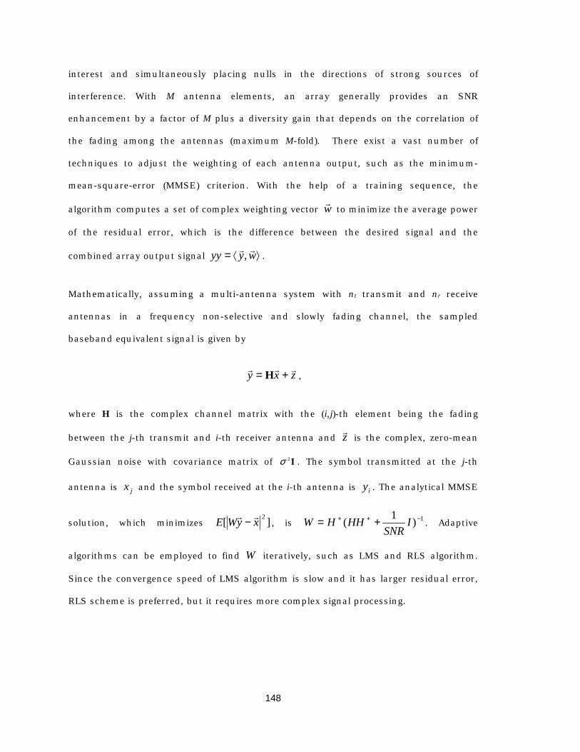
148
interest and simultaneously placing nulls in the directions of strong sources of
interference. With M antenna elements, an array generally provides an SNR
enhancement by a factor of M plus a diversity gain that depends on the correlation of
the fading among the antennas (maximum M-fold). There exist a vast number of
techniques to adjust the weighting of each antenna output, such as the minimum-
mean-square-error (MMSE) criterion. With the help of a training sequence, the
algorithm computes a set of complex weighting vector wr to minimize the average power
of the residual error, which is the difference between the desired signal and the
combined array output signal ⟩⟨= wyyy rr, .
Mathematically, assuming a multi-antenna system with nt transmit and nr receive
antennas in a frequency non-selective and slowly fading channel, the sampled
baseband equivalent signal is given by
zxy rrr += H ,
where H is the complex channel matrix with the (i,j)-th element being the fading
between the j-th transmit and i-th receiver antenna and zr is the complex, zero-mean
Gaussian noise with covariance matrix of I2σ . The symbol transmitted at the j-th
antenna is jx and the symbol received at the i-th antenna is iy . The analytical MMSE
solution, which minimizes ][ 2xyWE rr − , is 1)1( −++ += ISNR
HHHW . Adaptive
algorithms can be employed to find W iteratively, such as LMS and RLS algorithm.
Since the convergence speed of LMS algorithm is slow and it has larger residual error,
RLS scheme is preferred, but it requires more complex signal processing.
149
5.2.2.2 SVD algorithm
Again start with ZXYrrr
+= H , after performing singular value decomposition (SVD) on the
matrix H, it becomes
ZXYrrr
+∑= HVU .
If Xr
is any vector in nC , then HV will be absorbed into Xr
. As a result, it is impossible
to estimate V from the received signal at the receiver side. But it is possible to estimate
the min(r,t) dominant components of U up to a unitary transformation using signal
subspace estimation if the data on different transmit antennas are independent.
Further if uniform power allocation is used, the min(r,t) dominant components of both U
and ΣΣΣΣ can be estimated with considerable level of confidence. The receiver sends back
the sub-sampled versions of the demodulated signals to the transmitter for the
estimation of V. The transmitter then projects the transmitted information on the eigen-
modes of the channel with more information on the strong modes and less on the weak
modes. For example, if M-PSK is used as modulation scheme, M is chosen depending on
the strength of the eigen-modes estimated. A blind channel tracking algorithm, based
on signal subspace decomposition of the received data and periodic feedback of
information from receiver to transmitter, was developed for slowly flat fading channel
[Poon00].
5.2.2.3 Issues with multi-antenna system There are many design issues associated with a multi-antenna system, such as
150
• Achievable performance: since the capacity of a multi-antenna system strongly
depends on the channel condition, which is affected by the propagation
environment and antenna arrangement (for instance, to take the best possible
advantage of spatial diversity, the antennas have to be placed far enough apart
for small correlation), the achievable performance varies with the changing of
those parameters. For example, ideally, there are 4 independent “channels” in a
4 x 4 multi-antenna system, but simulations show that most of the time only 3
of them can be used for transmitting data with reasonable performance, i.e., the
singular value of the fourth channel is too small.
• Adaptation speed: unless stationary channel can be assumed for short packet-
based transmission, adaptive algorithms need to be used to track the time-
varying channel condition. The adaptation speed needs to be faster than the
Doppler spread.
• Convergence speed: the requirement on convergence speed depends on the
application, packet-based communications demand for fast convergence in the
interest of transmission efficiency, while continuous transmission can tolerate
longer convergence time for better performance.
• Requirement of feeding back channel information to the transmitter: some
algorithms, e.g., the SVD algorithm, require the transmitter to know the channel
information, thus a feedback link needs to be designed accordingly.
5.2.3 Multiple-access schemes Various types of multiple-access schemes exist: frequency division multiple access
(FDMA), time division multiple access (TDMA), code division multiple access (CDMA),
and carrier sense multiple access (CSMA). The first three are typically used in
communications systems where there is a central coordinator (such as a base station)
using time-domain duplex (TDD) or frequency-domain duplex (FDD) for downlink (from
base station to mobile) and uplink (from mobile to base station) traffic. Such centralized
systems are conventionally used for applications which require simultaneous and
synchronous multiple access, for example, the cellular system which is designed for
mobile voice communications. CSMA is an asynchronous type of TDMA and is

151
traditionally used for distributed packet-based communications between peers in a LAN
environment. There are two variations of CSMA: CSMA with collision avoidance
(CSMA/CA) and CSMA with collision detection (CSMA/CD) that requires a transceiver
to listen to the channel for collision while transmitting.
In the context of MCMA system, several multiple-access schemes can be applied,
depending on the applications. The following sections describe some possible
techniques.
5.2.3.1 MC-CDMA MC-CDAM (Multi-carrier CDMA) [Yee93, Fazel93, Chouly93] is a combination of CDMA
and OFDM, where each user is assigned a unique code from an orthogonal or near-
orthogonal code set and the multiple-access capability is achieved by spreading in
frequency domain. In other words, a fraction of the symbol (e.g., a chip of the spreading
code) is transmitted through a different sub-carrier. Note for multi-carrier transmission,
it is essential to have frequency non-selective fading over each sub-carrier. Therefore, if
the original symbol rate is high enough to become subject to frequency selective fading,
the signal needs to be serial-to-parallel converted before spreading. That is assigning
multiple codes to the high data rate user. The MC-CDMA receiver requires coherent
detection for successful dispreading operation. Multi-antenna processing needs to be
performed for each sub-carrier and for each simultaneous operating user in the base
station. Such a processing requirement is infeasible even when using the most
computationally simple multi-antenna algorithms. (For example, in the case of N = 64
sub-carriers and k = 64 users, the system would need a total of Nk = 4096 multi-
antenna processing units at the base station.)

152
5.2.3.2 OFDMA In OFDMA (Orthogonal Frequency Division Multiple Access), multiple-access is realized
by assigning each user a fraction of the available number of sub-carriers. In this way, it
is equal to ordinary FDMA, but OFDMA avoids the relatively large guard bands that are
necessary in FDMA to separate different users. There are different variations of this
scheme, such as frequency-hopping OFDMA where each user is assigned a different
hopping pattern. OFDMA can be combined with TDMA where each user only transmits
in a fraction of the available time slots. Also, a dynamic channel allocation algorithm
can be employed to avoid interference from other users, rather than averaging
interference as in CDMA systems. Moreover, it can provide variable data rate to different
users according to their application needs by assigning different numbers of sub-
carriers, resulting in a more flexible system.
A simple version of OFDMA is assigning each user a single sub-carrier, which can be
also looked as a special case of MC-CDMA with spreading code matrix being identity
matrix. This choice simplifies the system design since only one multi-antenna
processing unit is needed per user, consequently the base station only needs k multi-
antenna processing units instead of Nk. The main performance advantage of the more
complex scheme of MC-CDMA is interference averaging and protection against fading
since all users use all sub-carriers simultaneously. The hope is that the multi-antenna
processing can provide enough diversity gain for the system even with this simple
OFDMA scheme.
5.2.3.3 CSMA In this case, at any time only one user is transmitting data using all the N sub-carriers,
so only N multi-antenna processing units are needed in the transceiver. And except

153
performing carrier sensing, no extra signal processing is needed in addition to OFDM to
support multiple access.
5.3 System/Hardware co-design framework
A MCMA system is a complex communications system which is composed of many
sophisticated yet interacting signal processing blocks in the transmitter-channel-
receiver chain. Although these advanced signal processing techniques have been
extensively studied in theory, except for the most elementary techniques, they were
thought to be too complex to be implemented in energy and cost constrained portable
devices. The challenge is to design a system that achieves high performance with
reasonable implementation cost. To that end, design options, in terms of both algorithm
selections and implementation strategies, need to be explored at the system level. A
system design framework was developed to facilitate the exploration.
5.3.1 Overview The MCMA system is designed for applications such as providing multimedia access to
multiple portable terminals, intended for use in an indoor wireless environment. Several
key parameters are assumed for the system design: the delay spread is on the order of
100 ns, channel varies slowly due to pedestrian motions, data rate ranges from 1-10
Mbits/s per user, and there are 10’s of users in the system.
The design framework is implemented in Simulink. One major advantage of
implementing the framework in Simulink is its compatibility with MATLAB, which is
already widely used for the development and evaluation of communications algorithms.
The goal of this framework is to facilitate system and hardware co-design by 1) allowing
complete end-to-end simulations of communications systems, including all analog,

154
mixed-signal and digital components and 2) bridging the gap between system design
and hardware implementation through the use of the design and estimation
methodology presented in Chapter 2 with a high-level DSP kernel library presented in
Appendix A.
As discussed in previous chapters, there are multiple choices of algorithms for each
processing block, as well as multiple choices of implementation architectures for those
blocks. With many blocks in a MCMA system, the design choices multiply. And the
optimal design is usually not obvious, which require extensive analysis or simulations.
Especially for wireless communications systems, depending on the application
requirements and operating channel conditions, the optimal choice varies. Moreover,
some blocks are more sensitive to system parameter changes while others are not.
Since blocks are interacting with each other, changes made for one block may affect
others, or in some case, may require changes of the whole system structure. In order to
explore the trade-offs between different blocks, such as analog front-end impairments
and various digital signal processing algorithms, and the overall system performance, a
system level simulation framework is highly desirable.
Another main purpose of this framework is to provide hardware implementation
estimates, in terms of area, delay, and power consumption, to system designers to help
them make decisions on the trade-off between performance and implementation cost.
Under certain performance requirements, different algorithm or same algorithm with
different parameters can be chosen for a block, which may result in significantly
different implementations. For example, in order to maintain performance while
achieving minimum power consumption, it is obviously better to allocate more power
from the overall budget to blocks that are pivotal to the overall system performance. In
this framework, each block consists of two evaluation models, functional model and
architectural model, which are closely related to each other under a set of common

155
design parameters. Hence it enables simultaneous quantification of system performance
and implementation cost. Together they provide valuable insights to make system
design decisions.
The key design philosophies behind the system and block designs for this framework
are:
• Generic: blocks are designed as general, reusable modules with as less
assumption as possible on other blocks or system parameters so that any
MCMA-type systems can fit in this framework.
• Flexible: both the individual blocks and the overall systems are parameterized.
For example, blocks can use different word-length and systems can incorporate
different number of antennas and allocate different number of sub-carriers for
each user.
• Modular: efforts are made to keep a common interface for a block so that
multiple implementations are inter-changeable and a newly developed version of
a block can be plugged into the system simulation and tested without modifying
other blocks or breaking the system.
Consequently the key benefits of this framework are: 1) design knowledge encapsulation
facilitates design reuse and cooperation between designers and 2) generic, flexible, and
modular high-level block library enables fast design exploration. It should be noted that
this methodology can be applied to any DSP system design, the MCMA system is an
example of complex DSP systems to illustrate the design framework.
The following sections give the specifications and design examples of each of the main
blocks in the MCMA system. Associated with each block are: block diagram, the
description of functionality and interface, possible algorithms, performance simulations,
and Simulink implementation and parameters.
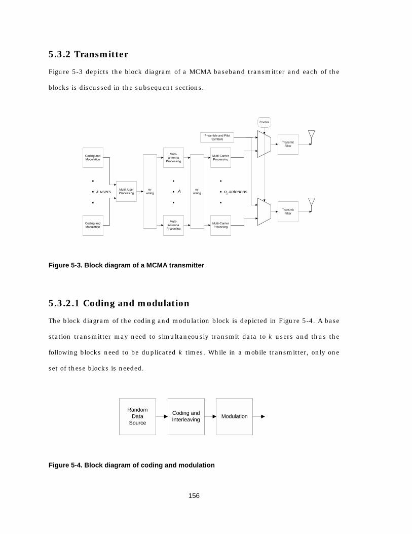
156
5.3.2 Transmitter Figure 5-3 depicts the block diagram of a MCMA baseband transmitter and each of the
blocks is discussed in the subsequent sections.
Coding andModulation
Multi-CarrierProcessing
Preamble and PilotSymbols
Control
TransmitFilter
Multi_UserProcessing
.
.
.
Coding andModulation
k users
.
.
.nt antennas
Multi-CarrierPrcoseiing
TransmitFilter
Multi-antenna
Processing
.
.
.
Multi-Antenna
Prcoseiing
re-wiring
re-wiringA
Figure 5-3. Block diagram of a MCMA transmitter
5.3.2.1 Coding and modulation The block diagram of the coding and modulation block is depicted in Figure 5-4. A base
station transmitter may need to simultaneously transmit data to k users and thus the
following blocks need to be duplicated k times. While in a mobile transmitter, only one
set of these blocks is needed.
RandomData
Source
Coding andInterleaving Modulation
Figure 5-4. Block diagram of coding and modulation

157
Random data source
Generates binary data for simulation purpose.
Coding and interleaving
• Possible coding schemes are:
• Block codes (e.g., Reed-Solomon code)
• Convolutional codes with parameters: base rate (e.g., 1/2), constraint
length (e.g., 7 which corresponding to 64-state), code generators (e.g., octal
133, 171), puncturing rate (e.g., 3/2). Turbo codes can be used to achieve
higher coding gain at the cost of increased implementation complexity and
decoding latency.
• Concatenated codes provide a larger coding gain with less implementation
complexity than comparable single codes. Usually, the inner code is a
convolutional code and the outer code is a block code. The motivation
behind this is that the convolutional code with soft decision decoding
performs better for relatively low input SNR. The hard decision block
decoder then cleans up the relatively few remaining errors in the decoded
output bits of the convolutional decoder. An interleaver is inserted
between two coders to break up bursts of errors as much as possible.
• Interleaving is a certain permutation of the coded bits. A commonly used
interleaving scheme is the block interleaver, where input bits are written in a
matrix (memory) column by column and read out row by row.
• Output rate = input data rate R * coding rate (e.g., base rate * puncturing rate).
This is coded data rate Rc.
• With multi-antenna processing, coding can be applied not only in time domain
but also in spatial domain, such as space-time coding. If channel information
would be fed back to this block from the receiver, adaptive modulation and
channel bit allocation and variable rate coding can be applied to optimize system
performance.
158
Modulation
Possible modulation schemes are: BPSK, QPSK, 16-QAM, and 64-QAM (quadrature
amplitude modulation with Gray coded constellation mappings).
As an alternative, coding and modulation can be combined together using Trellis-coded
modulation. It attains coding gain without bandwidth expansion by increasing the
constellation size. It was demonstrated in [Ungerboeck82] that coding gain up to 6 dB is
achievable by using Trellis-coded 8-PSK with rate of 2/3 coding compared to using un-
coded QPSK scheme.
5.3.2.2 Multi-antenna processing Transmitter-side multi-antenna processing requires the knowledge of the channel,
which is only possible in fixed-wireless communications or through the use of a
feedback link in mobile communications. As an example of transmitter-side multi-
antenna processing, the SVD algorithm projects the transmitted information onto the
eigen-modes of the channel. Most multi-antenna algorithms, such as the MMSE
algorithm, require receiver-side processing only, and at the transmitter the data stream
is split into parallel data streams feeding multiple antennas.
Since the multi-antenna processing needs to be performed for each sub-carrier
allocated to a user to send data, the number of processing units, A, depends on
multiple-access scheme as discussed in Section 5.2.3.
5.3.2.3 Multi-carrier processing Section 5.2.1 describes how the basic OFDM signal is formed. After possibly adding
pilots and empty bins, IFFT modulates a block of values onto sub-carriers, i.e., IFFT is
performed at N times slower rate. Adding cyclic prefix makes the output rate higher
than data symbol rate. The dominating processing of this block is IFFT, the
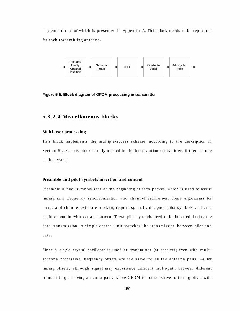
159
implementation of which is presented in Appendix A. This block needs to be replicated
for each transmitting antenna.
Serial toParallel IFFT Parallel to
Serial
Pilot andEmpty
ChannelInsertion
Add CyclicPrefix
Figure 5-5. Block diagram of OFDM processing in transmitter
5.3.2.4 Miscellaneous blocks
Multi-user processing
This block implements the multiple-access scheme, according to the description in
Section 5.2.3. This block is only needed in the base station transmitter, if there is one
in the system.
Preamble and pilot symbols insertion and control
Preamble is pilot symbols sent at the beginning of each packet, which is used to assist
timing and frequency synchronization and channel estimation. Some algorithms for
phase and channel estimate tracking require specially designed pilot symbols scattered
in time domain with certain pattern. These pilot symbols need to be inserted during the
data transmission. A simple control unit switches the transmission between pilot and
data.
Since a single crystal oscillator is used at transmitter (or receiver) even with multi-
antenna processing, frequency offsets are the same for all the antenna pairs. As for
timing offsets, although signal may experience different multi-path between different
transmitting-receiving antenna pairs, since OFDM is not sensitive to timing offset with

160
the insertion of cyclic prefix, the same timing can be used for all antenna paths.
Consequently, the tasks for timing and frequency synchronization are the same across
antennas. In this design, same pilots are sent from all the transmitting antennas and
the signals from all the receiving antennas are summed together for timing and
frequency synchronization. This scheme is equivalent to a signal antenna system, but
with lumped multi-path channel. Therefore, the synchronization algorithms for single
antenna system can be directly applied and only one implementation is needed for all
antennas.
Transmit filter
Typically, a digital raised cosine filter is used as the transmit filter. The main design
parameters are over-sampling rate and filter roll-off factor (= excess bandwidth).
MATLAB function “rcosfir” can be used to for the filter design, the smaller the roll-off
factor, the less the bandwidth expansion, but the more filter taps are needed to achieve
certain out-of-band rejection. After this transmit filter, digital signal will be converted to
analog signal and the over-sampling rate is one trade-off between the raised cosine filter
design and D/A converter design. For simulation purpose, the over-sampling rate is
chosen to be 4-8, in order to have a finer resolution of the channel model and better
noise model. The output rate of this block is over-sampling rate times input rate.
Instead of filtering, it is also possible to use time-domain windowing to reduce the out-
of-band spectrum since windowing and filtering are dual techniques.
5.3.3 Channel model For a wideband system, the frequency-selective channel is commonly modeled as a
tapped delay line with tap spacing of sampling period. The number of taps is
determined by (channel delay spread)/(sampling period). Extensive measurements of

161
the indoor radio channel reported that the typical delay spread values range between
100-400 ns. An exponentially decaying power profile with random phase is typically
assumed. For systems with multiple transmitter and receiver antennas, a channel
model must include the consideration of the correlation among antennas. Some multi-
antenna channel characterization has been carried out for narrowband channel, which
shows that most of the correlation is present in the main (i.e., line of sight) path. Using
these factors, a fairly simple channel model was developed in [Klein00].
In this design, a more realistic and accurate channel model can be used, which is based
on the data generated by ray-tracing simulations [Tang01]. The ray-tracing simulation
tool takes two-dimensional building floor plan and generates the data ),,( lllB φτ , i.e.,
(amplitude, delay, phase), for each multi-path component. With these data the received
signal can be calculated at any time instance. For a multi-antenna system, the multi-
path data are generated for each pair of transmitting and receiving antenna and
consequently the correlation among antennas elements are inherently taken into
account. Moreover, this channel model takes into consideration of the sampling error
(due to the offset between the baseband digital clock rate at transmitter and receiver).
Figure 5-6 depicts the discrete-input discrete-output channel model [Tang01]
implemented in Simulink. Since the channel introduces memory, i.e., the received
signal sample at a given time depends on the transmitted signals at earlier times, the
transmitted signal samples are kept for a certain period of time in the channel module
to calculate the received signal samples being affected. Also, when receiver sampling
period is longer than transmitter sampling period, special care is needed to ensure
casuality through the whole simulation time. In that case, a long enough sequence of
0’s is inserted before real signal starts transmitting.

162
Analog impairments Channel
ts
Discrete data flow
Bl, τ l, φl ∆fc, ∆φ(ts)
Transmitter time scale
Receiver time scale
Figure 5-6. Discrete channel model
Most of the time the portable terminal is stationary. The indoor wireless environment
changes due to motions occurring at human rate (e.g., people moving around or the
terminal is being moved), which is typically less than 3 m/s. Consequently, the
coherent time of the channel is assumed to be much greater than a symbol period and
Doppler effects are ignored. For the simulation purposes, the channel coherence time is
assumed to be approximately
speedmotionfrequncycarrierc
speedmotionlengthwave
⋅⋅=⋅
221
,
which is about 20 ms if the carrier frequency is 5 GHz. This number is also verified by
empirical measurements.
Simulink s-functions models were implemented in C, as shown in Figure 5-7. The
parameters for the “multipath channel for single antenna system” block are:
amplitudes, delays, and phases of all the multi-path components, carrier frequency,
sample period at transmitter, sample period at receiver, and start time for adding zero
sequence to ensure casuality. And the parameters for the “multipath channel for multi-
antenna system” block are: number of transmitters, number of receivers, number of
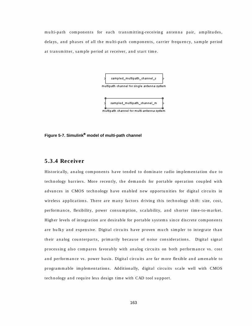
163
multi-path components for each transmitting-receiving antenna pair, amplitudes,
delays, and phases of all the multi-path components, carrier frequency, sample period
at transmitter, sample period at receiver, and start time.
Figure 5-7. Simulink model of multi-path channel
5.3.4 Receiver Historically, analog components have tended to dominate radio implementation due to
technology barriers. More recently, the demands for portable operation coupled with
advances in CMOS technology have enabled new opportunities for digital circuits in
wireless applications. There are many factors driving this technology shift: size, cost,
performance, flexibility, power consumption, scalability, and shorter time-to-market.
Higher levels of integration are desirable for portable systems since discrete components
are bulky and expensive. Digital circuits have proven much simpler to integrate than
their analog counterparts, primarily because of noise considerations. Digital signal
processing also compares favorably with analog circuits on both performance vs. cost
and performance vs. power basis. Digital circuits are far more flexible and amenable to
programmable implementations. Additionally, digital circuits scale well with CMOS
technology and require less design time with CAD tool support.
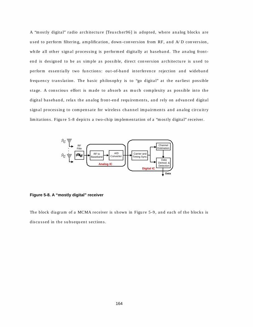
164
A “mostly digital” radio architecture [Teuscher96] is adopted, where analog blocks are
used to perform filtering, amplification, down-conversion from RF, and A/D conversion,
while all other signal processing is performed digitally at baseband. The analog front-
end is designed to be as simple as possible, direct conversion architecture is used to
perform essentially two functions: out-of-band interference rejection and wideband
frequency translation. The basic philosophy is to “go digital” at the earliest possible
stage. A conscious effort is made to absorb as much complexity as possible into the
digital baseband, relax the analog front-end requirements, and rely on advanced digital
signal processing to compensate for wireless channel impairments and analog circuitry
limitations. Figure 5-8 depicts a two-chip implementation of a “mostly digital” receiver.
RF to Baseband
A/D Converter
RF Filte
Analog IC
Carrier and Timing Sync.
ChannelEstimation
Data Demod. & Detection
Data
Digital IC
•••
Figure 5-8. A “mostly digital” receiver
The block diagram of a MCMA receiver is shown in Figure 5-9, and each of the blocks is
discussed in the subsequent sections.

165
Demodulationand Decoding
AnalogFront-end
AnalogFront-end
Multi-antenna
Processing
.
.
.
Multi-Antenna
Prcoseiing
re-wiring
re-wiring
.
.
.nr antennas
TimingSynchrnization
FrequencySynchronization
and PhaseTracking
Multi-CarrierProcessing
Multi-CarrierProcessing
AGC
A
Figure 5-9. Block diagram of a single user MCMA receiver
5.3.4.1 Analog front-end Since short simulation times are critical for rapid evaluation, behavioral models are
used for the analog front-end components. However, even if behavioral models are used,
simulating the analog front-end at the carrier frequency is unacceptable. For such a
simulation, the maximum step size must be based on the carrier frequency, whereas
the total number of steps must be based on the symbol rate. Since the carrier frequency
is typically much higher than the symbol rate in wireless communications systems,
such a simulation would be prohibitively slow. In order to decrease the simulation time,
baseband-equivalent models for the analog RF building blocks were developed [Yee01]
so that the time steps can be made appropriate to the signal bandwidth rather than the
carrier. The method is similar to envelope simulation techniques used in some RF
circuit-level simulators.
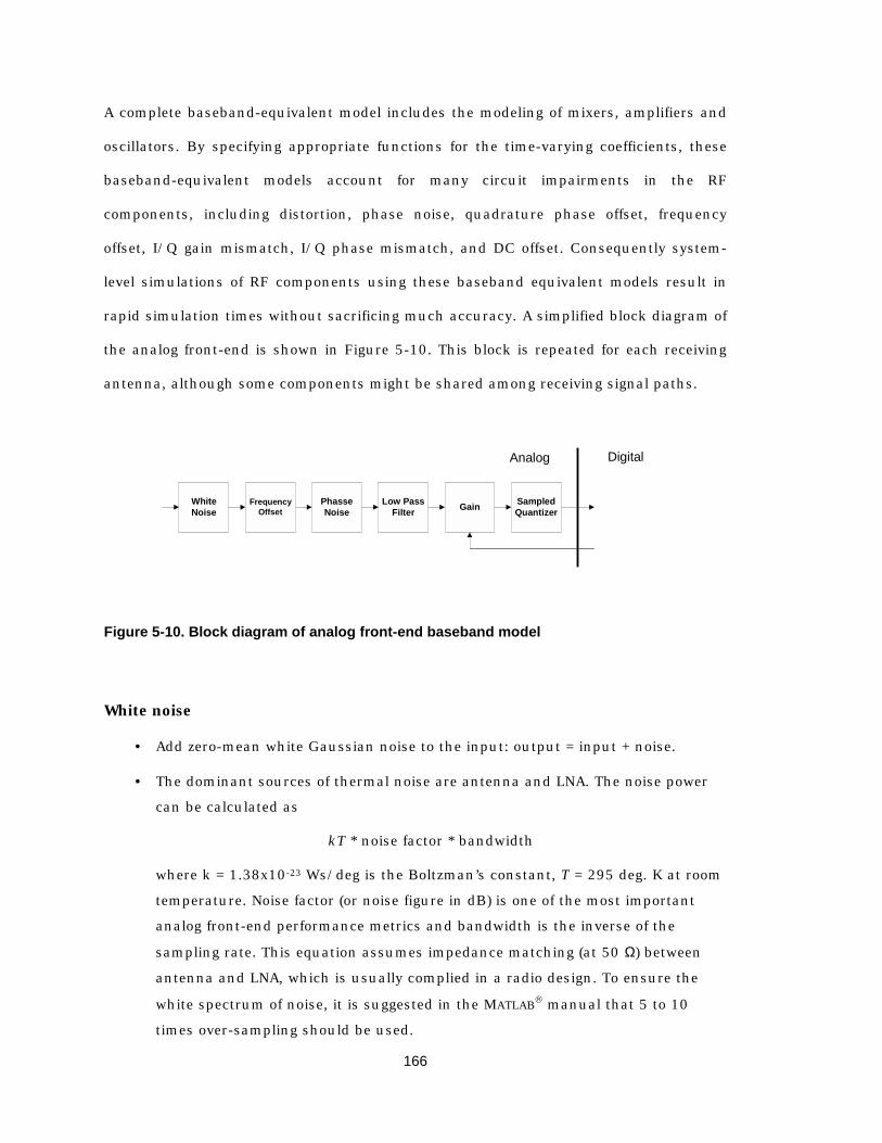
166
A complete baseband-equivalent model includes the modeling of mixers, amplifiers and
oscillators. By specifying appropriate functions for the time-varying coefficients, these
baseband-equivalent models account for many circuit impairments in the RF
components, including distortion, phase noise, quadrature phase offset, frequency
offset, I/Q gain mismatch, I/Q phase mismatch, and DC offset. Consequently system-
level simulations of RF components using these baseband equivalent models result in
rapid simulation times without sacrificing much accuracy. A simplified block diagram of
the analog front-end is shown in Figure 5-10. This block is repeated for each receiving
antenna, although some components might be shared among receiving signal paths.
WhiteNoise
FrequencyOffset
PhasseNoise
Low PassFilter Gain Sampled
Quantizer
Analog Digital
Figure 5-10. Block diagram of analog front-end baseband model
White noise
• Add zero-mean white Gaussian noise to the input: output = input + noise.
• The dominant sources of thermal noise are antenna and LNA. The noise power
can be calculated as
kT * noise factor * bandwidth
where k = 1.38x10⁻²³ Ws/deg is the Boltzman’s constant, T = 295 deg. K at room
temperature. Noise factor (or noise figure in dB) is one of the most important
analog front-end performance metrics and bandwidth is the inverse of the
sampling rate. This equation assumes impedance matching (at 50 Ω) between
antenna and LNA, which is usually complied in a radio design. To ensure the
white spectrum of noise, it is suggested in the MATLAB manual that 5 to 10
times over-sampling should be used.

167
Frequency offset
• Output = input * exp(j * 2π * frequency offset * time)
• Model the carrier frequency offset between transmitter and receiver.
Frequency offset = carrier frequency * crystal offset difference
The smaller the crystal offset, the more expensive the crystal. Typically crystal
offsets of 20-50 ppm (parts per million) are used in wireless communications
systems. The crystal offset difference is the difference between the crystal offset
at transmitter and receiver, so the worst case condition is a crystal offset
difference of 100 ppm.
Phase noise
• Output = input * exp(j * phase noise)
• The phase noise is modeled as a random process that has a 1/f2 spectrum which
is extrapolated from the single-sided phase noise specified at one offset
frequency. A low frequency phase noise ceiling (dBc/Hz) is another parameter
which needs to be specified to limit rms phase jitter.
Low pass filter
• Model the concatenated filters in the analog front-end. The higher the filter
order, the sharper the filter performance at the cost of increased implementation
complexity. Filter orders up to 6 or so can be implemented with reasonable cost.
To avoid signal degradation, passband bandwidth should be at least the signal
bandwidth.
Gain
• Output = input * gain
• There are two parts of the total gain through the analog front-end signal path:
fixed and variable. The variable gain is controlled by a signal fed back from a
digital signal processing unit AGC (automatic gain control).

168
Sampled Quantizer
• Sampled quantizer with clipping models A/D converter. A/D converter separates
the analog and digital domain: converting signal of continuous value in
continuous time to signal of discrete values at discrete time steps. The
quantization noise is determined by the precision and the clipping level is
determined by the dynamic range. Typically accuracy of 8-12 bits is sufficient
for wireless receivers.
• The sampling rate should be at least baseband signal rate if perfect sampling
time is known. Otherwise, the A/D should be sampled at Nyquist rate (=
baseband signal rate + bandwidth expansion of the raised cosine filter at the
transmitter) or higher rate if interpolation filter is employed in the digital signal
processing for timing adjustment.
5.3.4.2 Timing synchronization Timing synchronization (OFDM frame detection) is to detect the starting point of an
OFDM symbol in order to take N samples and perform FFT. It is one of the very first
things a receiver needs to perform properly to detect data from a packet and it enables
the operations of all other digital signal processing blocks. If there is a lost detection of
OFDM frame, the whole packet will be lost. On the other hand, if there is a false
detection, all the processing is wasted until some checking mechanism figures it out.
And since timing synchronization is stopped during that period, a packet might be lost
potentially. Hence, the timing synchronization needs to be deigned for robust operation
in the presence of multi-path channel and noise.
Timing synchronization can be performed using either the cyclic prefix or preamble. The
cyclic prefix is a duplicate of the signal at the end of an OFDM frame, i.e., the Ng
transmitted signal samples at the beginning of an OFDM symbol are exactly the same
as those N samples away. This feature can be utilized at the receiver to find the starting
point of an OFDM symbol by correlating the signal values N samples apart and looking
for a peak of length Ng. This scheme requires that noise is relatively small compared to

169
signal since noise will blur the correlation peak. Moreover, in the presence of multi-path
propagation, the signal samples at the beginning and end of the OFDM symbol are
“contaminated” by delay replicas of different previous signals. As a result, the
correlation peak can be very noisy.
A more reliable scheme is using preamble, a known time-domain signal sequence, for
timing synchronization. This technique is similar to timing synchronization in a CDMA
system. Different preambles can be designed for this purpose. For example, repetitions
of a short training sequence can be used, as in IEEE 802.11a standard. The presence of
a packet can be detected by correlating a short symbol with the next and detecting if
the correlation magnitude exceeds certain threshold. Another way to construct a
preamble is using a PN sequence. The performance of a PN sequence based timing
synchronization is evaluated below.
A PN sequence (= maximum length shift register sequence) is chosen because of its good
auto-correlation property: the correlation between a length of Nc PN sequence and any
delayed/shifted version of that sequence (which is another PN sequence of the same PN
family) is –1/Nc times smaller than the self-correlation. This property protects against
multi-path delay spread. Since timing synchronization is performed before frequency
and phase synchronization, a differential coding scheme is adopted. Padding is inserted
at both the head and tail of the sequence to make it a repetitive sequence for better
correlation results. (Because when the PN correlating sequence is shifting out of the
alignment, it is actually correlating with only part of a PN sequence and the rest is non-
PN signal, a repetitive PN sequence makes the desired correlation property valid for a
longer period.) The padding length is chosen, in this example, to make the timing
synchronization preamble the same length as an OFDM symbol.
Let the PN sequence be )]1(...),1(),0([ −= cNdddD , the transmitter sends out a
differential PN sequence as timing synchronization preamble:

170
)]1()1()(...),1()1()2(),0()0()1(),0([ −⋅−=⋅=⋅= ccc NdNsNsdssdsss .
At the receiver, a sliding-window correlator computes
TtidikyikykScN
i<≤⋅++⋅+= ∑
−
=
0),()1()()(1
0
*
where y is the received signal. The correlation metric is the power of S(k), i.e.,
)()()( *2 kSkSkS ⋅= .
The algorithm can be stated as searching for the first correlation metric that is larger
than the average by a certain threshold and is the maximum over the next Nc metrics.
The average is computed over a certain window size and the maximum peak over a
certain window size is searched because the use of differential coding, which can cause
spurious peaks with multi-path channel. The received signal y includes all the delayed
replicates of the transmitted differential PN sequence scaled by multi-path channel
gains. The calculation of the correlation metric at the receiver involves )1()( * +⋅ kyky ,
which produces not only the desired PN sequence, but also the products of the PN
sequence and its delayed (= shifted) versions. Since the product of two PN sequence of
the same PN family is another PN sequence of the family, i.e., a shifted version of the
desired PN sequence, more than one correlation peaks may occur, which are scaled by
the amplitudes of different multi-path components. The maximum peak corresponds to
the channel path with maximum gain. Because only the peak of delay spread is
detected, the cyclic prefix length should be double the maximum delay spread in order
to ensure the correct behavior with extreme cases, i.e., peak at either edge of the delay
spread profile.
The choice of threshold value is a trade-off between lost detection and false detection in
the presence of noise. The larger the threshold, the less possible false detection will
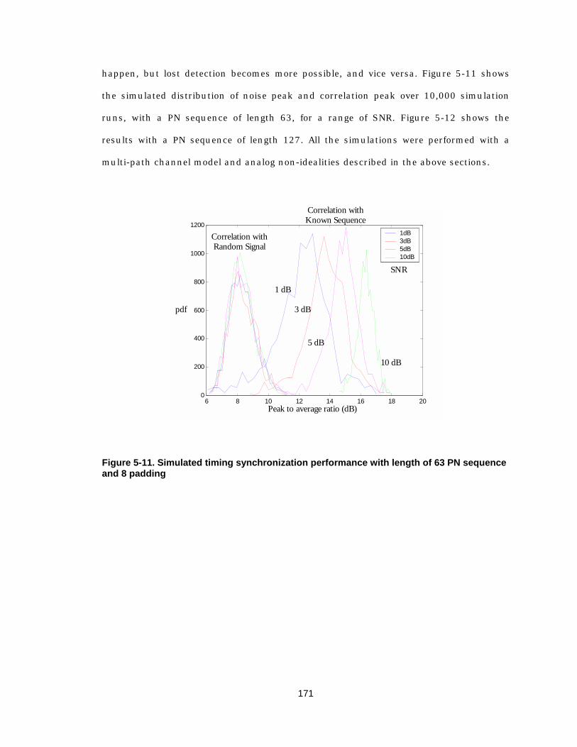
171
happen, but lost detection becomes more possible, and vice versa. Figure 5-11 shows
the simulated distribution of noise peak and correlation peak over 10,000 simulation
runs, with a PN sequence of length 63, for a range of SNR. Figure 5-12 shows the
results with a PN sequence of length 127. All the simulations were performed with a
multi-path channel model and analog non-idealities described in the above sections.
6 8 10 12 14 16 18 200
200
400
600
800
1000
12001dB 3dB 5dB 10dB
1 dB
3 dB
5 dB
10 dB
Peak to average ratio (dB)
SNR
Correlation with Random Signal
Correlation with Known Sequence
Figure 5-11. Simulated timing synchronization performance with length of 63 PN sequence and 8 padding
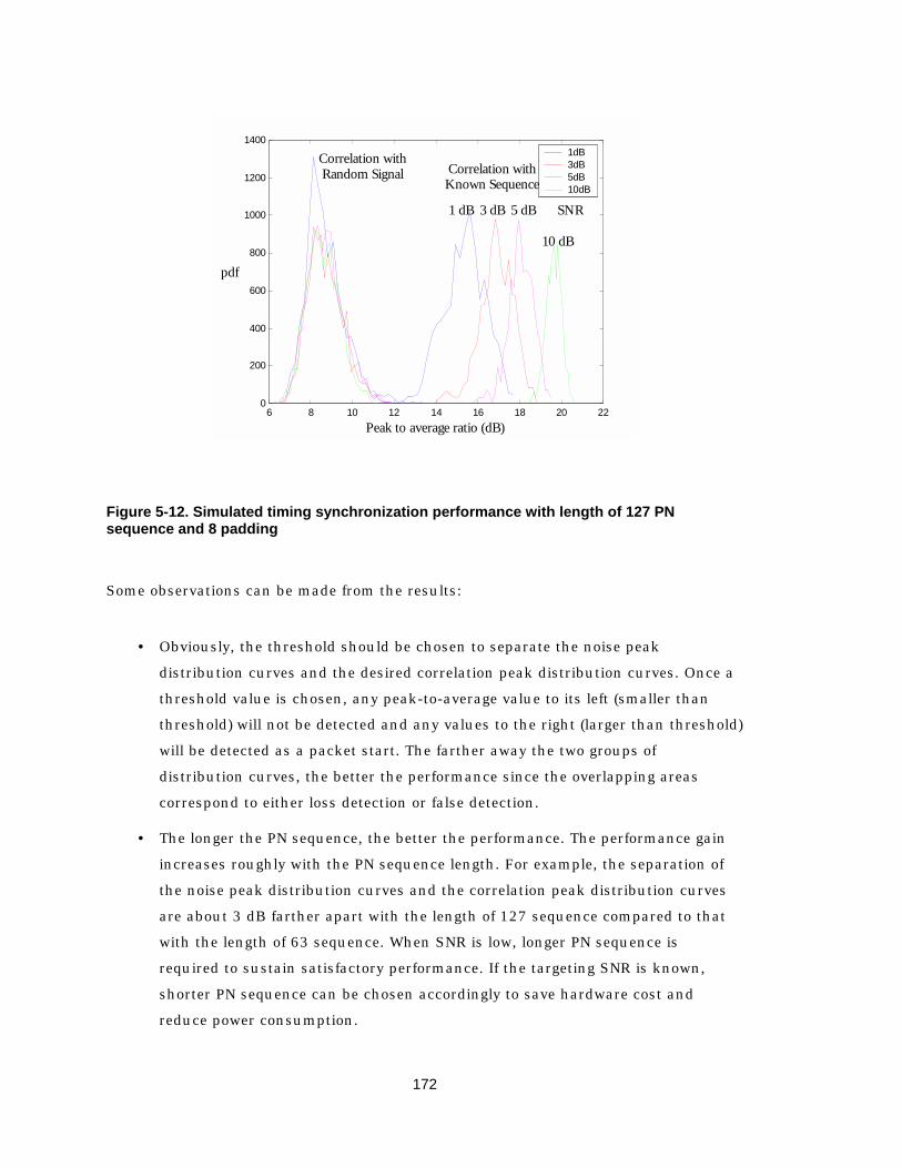
172
6 8 10 12 14 16 18 20 220
200
400
600
800
1000
1200
14001dB 3dB 5dB 10dB
1 dB 3 dB 5 dB
10 dB
Peak to average ratio (dB)
SNR
Correlation with Random Signal Correlation with
Known Sequence
Figure 5-12. Simulated timing synchronization performance with length of 127 PN sequence and 8 padding
Some observations can be made from the results:
• Obviously, the threshold should be chosen to separate the noise peak
distribution curves and the desired correlation peak distribution curves. Once a
threshold value is chosen, any peak-to-average value to its left (smaller than
threshold) will not be detected and any values to the right (larger than threshold)
will be detected as a packet start. The farther away the two groups of
distribution curves, the better the performance since the overlapping areas
correspond to either loss detection or false detection.
• The longer the PN sequence, the better the performance. The performance gain
increases roughly with the PN sequence length. For example, the separation of
the noise peak distribution curves and the correlation peak distribution curves
are about 3 dB farther apart with the length of 127 sequence compared to that
with the length of 63 sequence. When SNR is low, longer PN sequence is
required to sustain satisfactory performance. If the targeting SNR is known,
shorter PN sequence can be chosen accordingly to save hardware cost and
reduce power consumption.
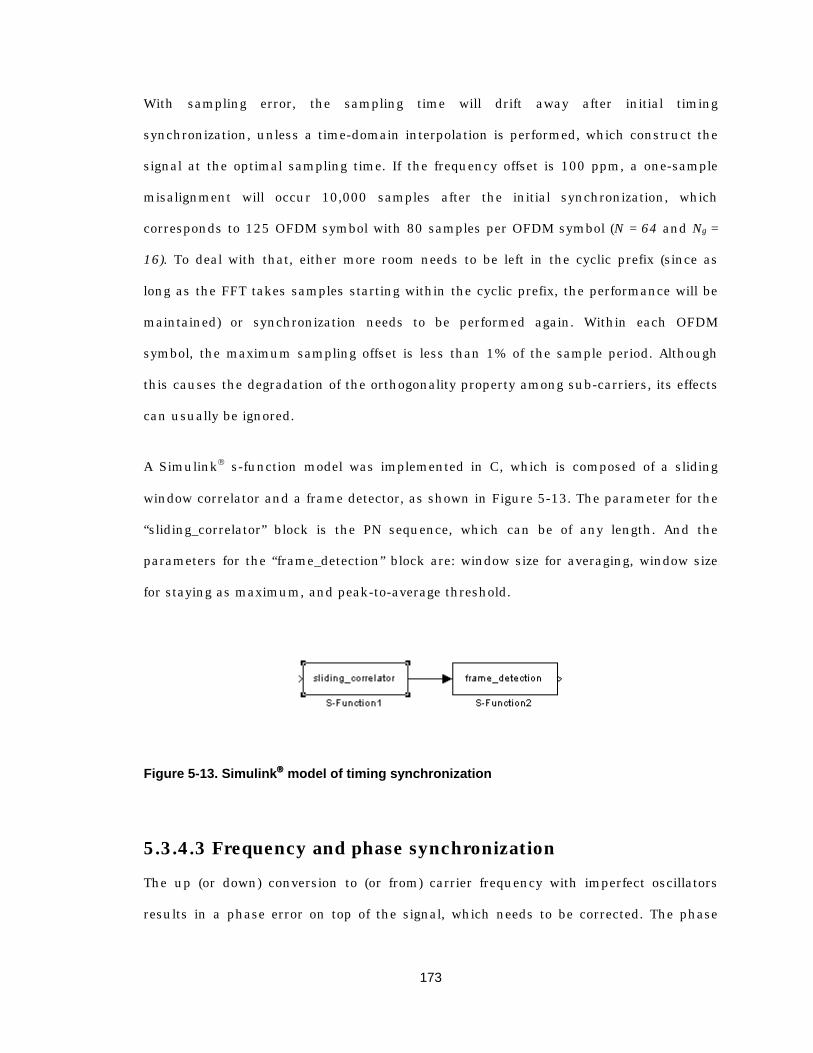
173
With sampling error, the sampling time will drift away after initial timing
synchronization, unless a time-domain interpolation is performed, which construct the
signal at the optimal sampling time. If the frequency offset is 100 ppm, a one-sample
misalignment will occur 10,000 samples after the initial synchronization, which
corresponds to 125 OFDM symbol with 80 samples per OFDM symbol (N = 64 and Ng =
16). To deal with that, either more room needs to be left in the cyclic prefix (since as
long as the FFT takes samples starting within the cyclic prefix, the performance will be
maintained) or synchronization needs to be performed again. Within each OFDM
symbol, the maximum sampling offset is less than 1% of the sample period. Although
this causes the degradation of the orthogonality property among sub-carriers, its effects
can usually be ignored.
A Simulink s-function model was implemented in C, which is composed of a sliding
window correlator and a frame detector, as shown in Figure 5-13. The parameter for the
“sliding_correlator” block is the PN sequence, which can be of any length. And the
parameters for the “frame_detection” block are: window size for averaging, window size
for staying as maximum, and peak-to-average threshold.
Figure 5-13. Simulink model of timing synchronization
5.3.4.3 Frequency and phase synchronization The up (or down) conversion to (or from) carrier frequency with imperfect oscillators
results in a phase error on top of the signal, which needs to be corrected. The phase
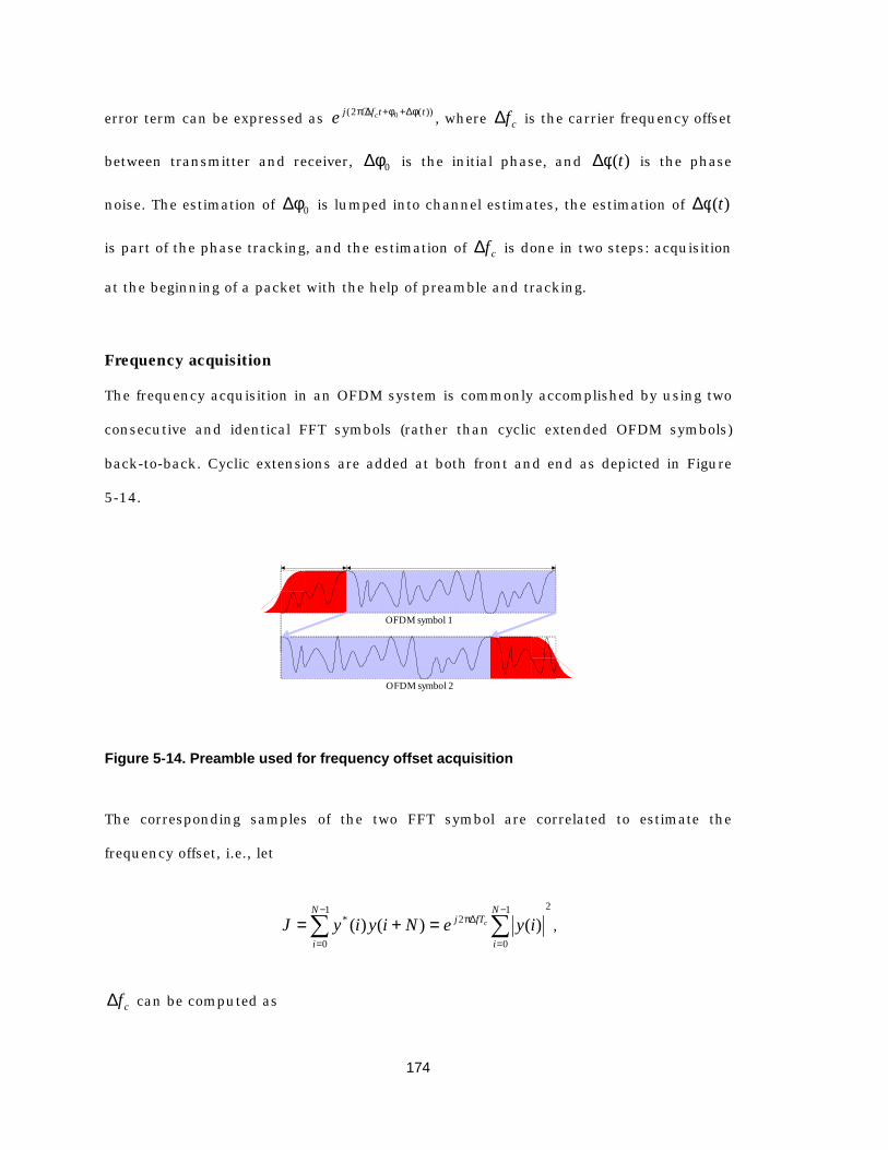
174
error term can be expressed as ))(2( 0 ttfj ce φ∆+φ+∆⋅π , where cf∆ is the carrier frequency offset
between transmitter and receiver, 0φ∆ is the initial phase, and )(tφ∆ is the phase
noise. The estimation of 0φ∆ is lumped into channel estimates, the estimation of )(tφ∆
is part of the phase tracking, and the estimation of cf∆ is done in two steps: acquisition
at the beginning of a packet with the help of preamble and tracking.
Frequency acquisition
The frequency acquisition in an OFDM system is commonly accomplished by using two
consecutive and identical FFT symbols (rather than cyclic extended OFDM symbols)
back-to-back. Cyclic extensions are added at both front and end as depicted in Figure
5-14.
OFDM symbol 1
OFDM symbol 2
Figure 5-14. Preamble used for frequency offset acquisition
The corresponding samples of the two FFT symbol are correlated to estimate the
frequency offset, i.e., let
21
0
21
0
* )()()( ∑∑−
=
∆π−
=
=+=N
i
fTjN
iiyeNiyiyJ c ,
cf∆ can be computed as

175
)(2
1 JangleT
fc π=∆ ,
which can be determined without ambiguity if π<∆π≤π− Tfc2 .
For the example design, assuming 5.25 GHz carrier frequency (the middle of 5.15-5.35
GHz band) with a total frequency offset of 100 ppm between transmitter and receiver,
20 MHz sample rate, and 64 sub-carriers,
68.1641020
1)10100(1025.5 669 ±=×
×××±××=∆ −Tfc ,
which is larger than the range specified above. Two possible ways to handle this are:
• Using additional two short repetitive symbols for coarse frequency offset
estimation, i.e., by making T shorter, the range of cf∆ which can be determined
without ambiguity becomes larger. The accuracy is coarser since with fixed
sample rate, shorter T means less number of noisy samples to average. So a
precise estimation based on long symbols is still needed to correct the coarse
estimate. This method is adopted in IEEE 802.11a standard.
• Decompose the estimation of )(22 β+απ=∆π Tfc into two parts: fractional part
β and integer part α . First, the fractional part ( ),[ ππ−∈ ) is estimated using
the method described above, and then the samples are corrected accordingly.
Mathematically, assuming the transmitted signal is
2/2/,)(1)(12/
2/
2NnNekU
Nnu
N
Nk
nNkj
<≤−= ∑−
−=
π,
at the receiver, after passing through the fading channel and adding frequency
offset, the signal becomes
2/2/,)()(1)(12/
2/
2)(2NnNekUkC
Neny
N
Nk
nNkj
Nnj
<≤−= ∑−
−=
πβ+απ.
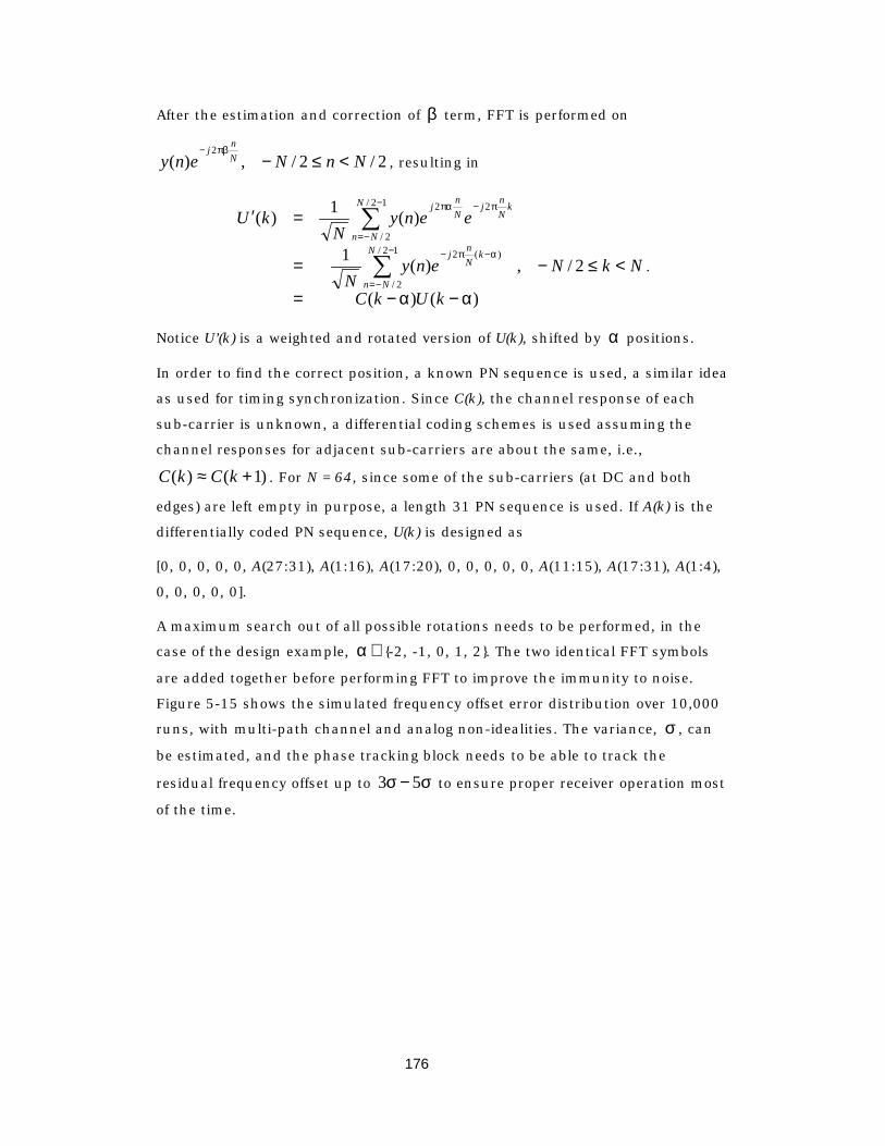
176
After the estimation and correction of β term, FFT is performed on
2/2/,)(2
NnNeny Nnj
<≤−πβ−
, resulting in
NkN
kUkC
enyN
eenyN
kU
N
Nn
kNnj
N
Nn
kNn
jNn
j
<≤−
α−α−=
=
=′
∑
∑−
−=
α−π−
−
−=
π−πα
2/,
)()(
)(1
)(1)(
12/
2/
)(2
12/
2/
22
.
Notice U’(k) is a weighted and rotated version of U(k), shifted by α positions.
In order to find the correct position, a known PN sequence is used, a similar idea
as used for timing synchronization. Since C(k), the channel response of each
sub-carrier is unknown, a differential coding schemes is used assuming the
channel responses for adjacent sub-carriers are about the same, i.e.,
)1()( +≈ kCkC . For N = 64, since some of the sub-carriers (at DC and both
edges) are left empty in purpose, a length 31 PN sequence is used. If A(k) is the
differentially coded PN sequence, U(k) is designed as
[0, 0, 0, 0, 0, A(27:31), A(1:16), A(17:20), 0, 0, 0, 0, 0, A(11:15), A(17:31), A(1:4),
0, 0, 0, 0, 0].
A maximum search out of all possible rotations needs to be performed, in the
case of the design example, ∈α -2, -1, 0, 1, 2. The two identical FFT symbols
are added together before performing FFT to improve the immunity to noise.
Figure 5-15 shows the simulated frequency offset error distribution over 10,000
runs, with multi-path channel and analog non-idealities. The variance, σ , can
be estimated, and the phase tracking block needs to be able to track the
residual frequency offset up to σ−σ 53 to ensure proper receiver operation most
of the time.

177
-0.1 -0.08 -0.06 -0.04 -0.02 0 0.02 0.04 0.06 0.08 0.10
200
400
600
800
1000
12001dB 3dB 5dB 10dB
1 dB
3 dB
5 dB
10 dB
Frequency estimation error
SNR
Figure 5-15. Simulated performance of frequency offset acquisition
Figure 5-16. Simulink model of frequency offset acquisition

178
A Simulink model, “Freq. Est”, was made based on the algorithm described in this
section. It is enabled by the timing synchronization block, and it takes the A/D
converted signal, and outputs the frequency offset estimate. The Simulink model is
depicted in Figure 5-16.
Phase tracking
Phase tracking is required for coherent detection to deal with residual frequency offset
error after the initial acquisition as well as phase noise. There are three types of
tracking techniques:
• Using pilot channels: a few sub-carriers do not carry data and these known sub-
carriers are used to track the common phase drift on all sub-carriers. This
method is adopted in IEEE 802.11a standard.
• Using pilot symbols: specially designed pilot symbols are scattered in the packet
to track the accumulated phase drift.
• Using decision-directed method: decisions on detected data are used for
tracking. This method is most efficient since it does not require extra pilot
channels or symbols and keeps tracking of all the sub-carriers all the time. A
feedback loop is formed, depicted as dotted lines in Figure 5-9. The decision is
based on results either after demodulation or after the decoding. Decisions after
decoding are more reliable but have longer latency.
First, a pilot symbol based tracking algorithm is evaluated, which is feed-forward only
processing. The basic idea is to increase the distance between the correlating symbols
to get more accurate estimation. Since Tfc∆ is being estimated with fixed accuracy, i.e.,
a given error variance of δ , larger T makes the error variance of cf∆ smaller as long as
π<∆π≤π− Tfc2 . Starting from the initial estimation, the distance between the pilot
symbols is increased incrementally so as the estimation accuracy. The data symbols are
sent between pilots. With higher frequency offset estimation accuracy, more symbols
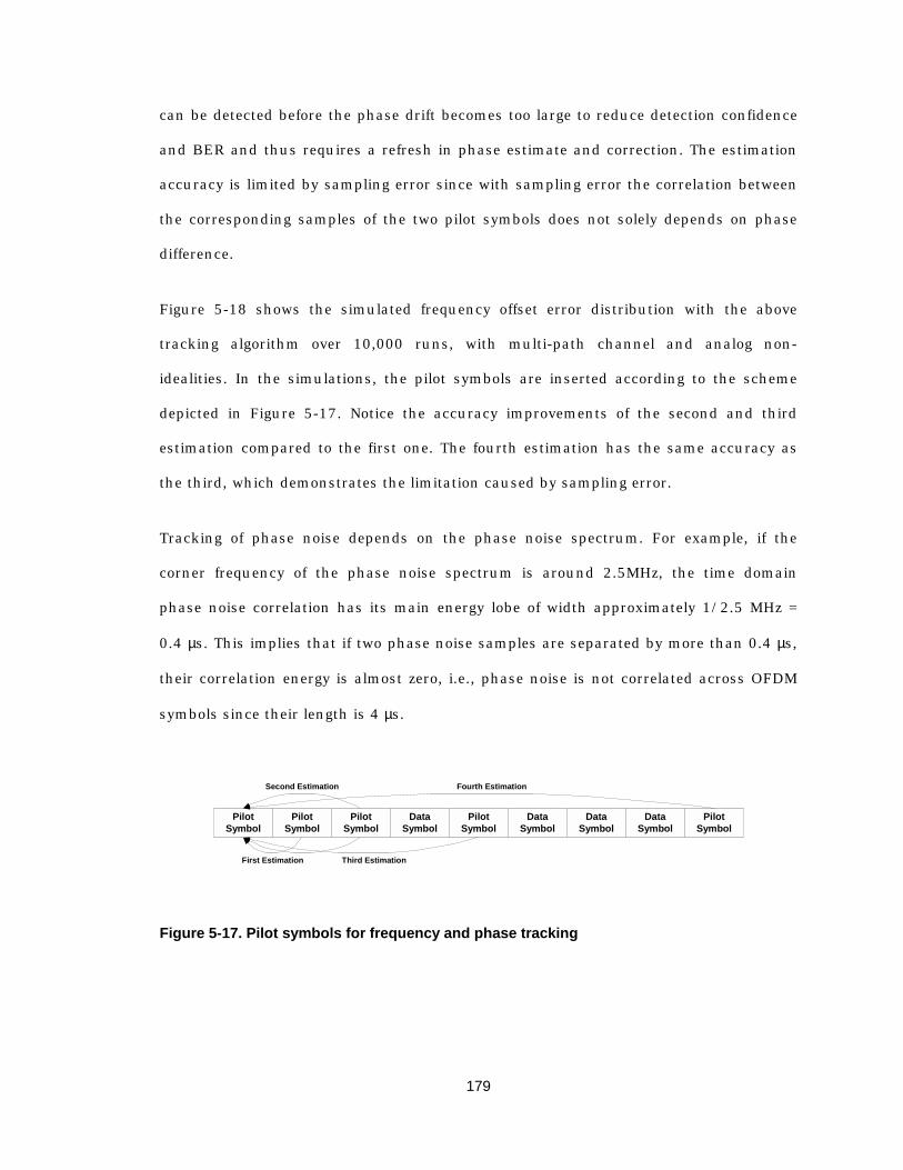
179
can be detected before the phase drift becomes too large to reduce detection confidence
and BER and thus requires a refresh in phase estimate and correction. The estimation
accuracy is limited by sampling error since with sampling error the correlation between
the corresponding samples of the two pilot symbols does not solely depends on phase
difference.
Figure 5-18 shows the simulated frequency offset error distribution with the above
tracking algorithm over 10,000 runs, with multi-path channel and analog non-
idealities. In the simulations, the pilot symbols are inserted according to the scheme
depicted in Figure 5-17. Notice the accuracy improvements of the second and third
estimation compared to the first one. The fourth estimation has the same accuracy as
the third, which demonstrates the limitation caused by sampling error.
Tracking of phase noise depends on the phase noise spectrum. For example, if the
corner frequency of the phase noise spectrum is around 2.5MHz, the time domain
phase noise correlation has its main energy lobe of width approximately 1/2.5 MHz =
0.4 µs. This implies that if two phase noise samples are separated by more than 0.4 µs,
their correlation energy is almost zero, i.e., phase noise is not correlated across OFDM
symbols since their length is 4 µs.
PilotSymbol
PilotSymbol
PilotSymbol
DataSymbol
PilotSymbol
DataSymbol
DataSymbol
DataSymbol
PilotSymbol
First Estimation
Second Estimation
Third Estimation
Fourth Estimation
Figure 5-17. Pilot symbols for frequency and phase tracking

180
-0.06 -0.04 -0.02 0 0.02 0.04 0.060
100
200
300
400
500
600
700
800
900
First estimation
Second estimation
Third estimation
Fourth estimation
Frequency estimation error
Figure 5-18. Simulated performance of frequency tracking (SNR=5dB)
Second, a decision-directed phase-lock-loop (PLL) was designed [Stimming01] as an
alternative frequency offset and phase noise tracking method. It is composed of a
second-order loop filter for phase correction before FFT (multi-carrier processing) and a
first-order loop filter for phase correction of each sub-carrier after FFT. Figure 5-19
shows the simulated performance of the PLL with residual frequency offset, where small
offset corresponds to 01.02 , ≈∆π Tf residuec and large offset corresponds to
1.02 , ≈∆π Tf residuec , and phase noise is assumed to have a 1/f2 dropping spectrum with
-100 dBc/Hz at low frequency until 2.5 MHz . The results show that even with very
small residual frequency offset error and phase noise, the phase error will build up.
Thus, if the transmission is more than 20-40 symbols, tracking of the phase becomes
necessary for coherent detection. This figure shows the convergence of the phase lock
loop. It takes longer to converge with larger initial error, so the requirement on the PLL
depends on the performance of frequency offset acquisition block. Also, the PLL helps to
deal with low frequency phase noise.
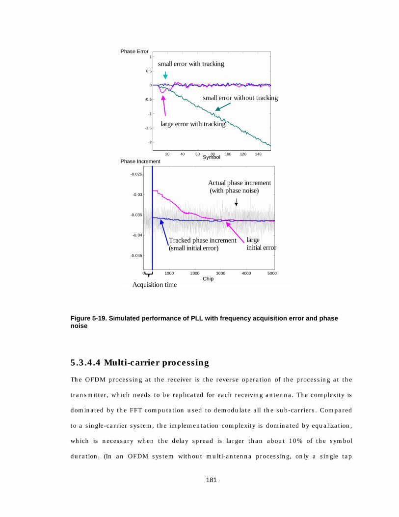
181
0 1000 2000 3000 4000 5000
-0.045
-0.04
-0.035
-0.03
-0.025
Acquisition time
20 40 60 80 100 120 140
-2
-1.5
-1
-0.5
0
0.5
1
small error with tracking
small error without tracking
large error with tracking
Actual phase increment (with phase noise)
Tracked phase increment(small initial error)
large initial error
Symbol
Phase Error
Chip
Phase Increment
Figure 5-19. Simulated performance of PLL with frequency acquisition error and phase noise
5.3.4.4 Multi-carrier processing The OFDM processing at the receiver is the reverse operation of the processing at the
transmitter, which needs to be replicated for each receiving antenna. The complexity is
dominated by the FFT computation used to demodulate all the sub-carriers. Compared
to a single-carrier system, the implementation complexity is dominated by equalization,
which is necessary when the delay spread is larger than about 10% of the symbol
duration. (In an OFDM system without multi-antenna processing, only a single tap

182
equalizer, or say, phase correction, is needed for coherent detection.) It is demonstrated
that the processing complexity of an OFDM modem can be significantly less than that of
a single carrier modem, given the fact that both can deal with the same amount of delay
spread [Nee00]. The reason is mainly due to the efficiency of the FFT algorithm, which is
a block processing technique and demodulates all N sub-carriers simultaneously. The
complexity difference grows with the bandwidth and delay spread product, which is a
measure of the relative amount of inter-symbol interference. The complexity, measured
by the number of multiplication per second grows quadratically with the bandwidth and
delay spread product in the equalizer. While for FFT, it grows only slightly faster than
linear since the number of multiplication per FFT is NN2log
2. Hence, OFDM is more
attractive than a single carrier system with equalization for relatively large bandwidth
and delay spread products.
Serial toParallel FFT Parallel to
SerialRemove
Cyclic Prefix
SelectUseful
Carriers
Figure 5-20. Block diagram of OFDM processing in receiver
5.3.4.5 Multi-antenna processing The multi-antenna processing essentially performs channel estimation and correction,
interference suppression, and optimal signal combining. Depending on the multiple-
access scheme, A multi-antenna processing units are required, as discussed in Section
5.2.3. Example algorithms are described in Section 5.2.2. The MMSE algorithm can be
implemented by a QRD-RLS block with about 3.5 mm2 silicon area and about 2.5 mW
power in a 0.25 µm technology, which is presented in Chapter 3. An estimate of the
183
implementation of SVD algorithm showed 9 mm2 silicon area and 55 mW power per
unit in the same technology [Markovic00]. A prototyping V-BLAST system was build by
Bell Labs [Wolniansky98]. It achieves a tenth of real-time operation, which is 650 kbps,
uses 4 TI DSP’s (floating-point TMS32C40 processors) and consumes 7W of power.
Coherent multi-antenna processing requires the estimation and correction of frequency
and phase offsets. Perfect synchronization is often assumed when developing and
evaluating multi-antenna algorithms and the effects of residual frequency and phase
offsets on the performance are neglected. However, some algorithms are very sensitive
to those offsets and put extremely high accuracy requirement on the synchronization
blocks, which may require very long preamble and thus reduces the transmission
efficiency of packet-based communications systems. Moreover, with the presence of
various noise sources in a wireless system and the time-varying feature of multi-path
channel and phase noise, there is a limit on achievable estimation accuracy that multi-
antenna algorithms have to tolerate. Adaptive multi-antenna algorithms can track the
frequency and phase offsets to a certain extent, typically the very low frequency
components. But they still have accuracy requirements on the synchronization blocks
to ensure proper operations. This is one example of inter-block relationships which
need to be studied for a complete system design. With the proposed system design
framework, the end-to-end transceiver chain can be simulated. Consequently the
specifications of interacting blocks and the trade-offs can be made accordingly.
For example, Figure 5-21 shows the simulation results of the MMSE-based multi-
antenna processing in the presence of residual frequency offset, where small offset
corresponds to 001.02 , ≈∆π Tf residuec and large offset corresponds to
06.02 , ≈∆π Tf residuec . Without phase tracking, the QRD-RLS filter will converge and
achieve high SNR at the beginning and quickly the phase error gets accumulated and
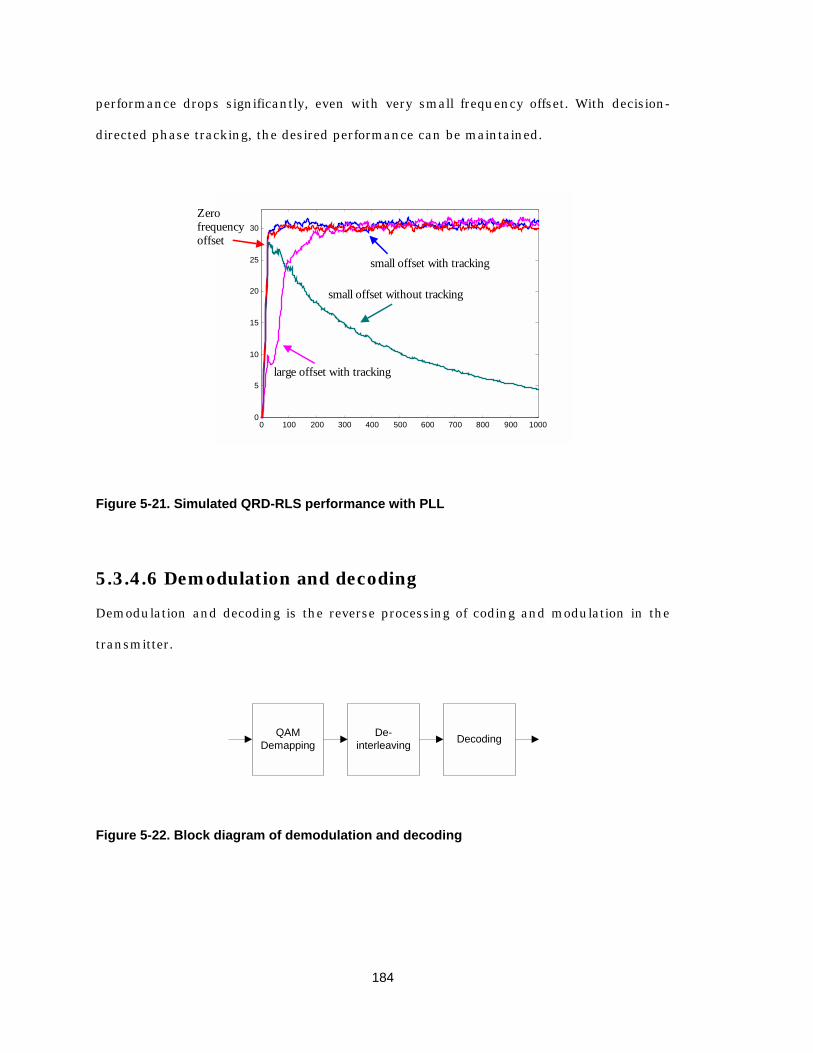
184
performance drops significantly, even with very small frequency offset. With decision-
directed phase tracking, the desired performance can be maintained.
0 100 200 300 400 500 600 700 800 900 10000
5
10
15
20
25
30
Zero frequency offset
small offset with tracking
small offset without tracking
large offset with tracking
Figure 5-21. Simulated QRD-RLS performance with PLL
5.3.4.6 Demodulation and decoding Demodulation and decoding is the reverse processing of coding and modulation in the
transmitter.
De-interleaving DecodingQAM
Demapping
Figure 5-22. Block diagram of demodulation and decoding

185
5.3.4.7 Miscellaneous blocks
Phase correction
To correct the phase offset estimated by frequency synchronization and phase tracking
blocks, the received signal needs to be rotated, i.e., multiplied by φ∆− je , where φ∆ is
the estimated phase offset. This function, exponential and multiplication, is typically
performed by a CORDIC block, the implementation of which is discussed in Appendix A.
Automatic gain control (AGC)
Receiver gain is one of the very first things that need to be set properly. After signal
detection, the signal power is averaged and the gain is determined to scale the input
power to the dynamic range of the A/D converter with some safety margin in order to
prevent a large amount of clipping. For example, the preamble in IEEE 802.11a is
composed of 10 short symbols and the first six can be used for setting AGC gain. The
AGC can be disabled afterwards and thus the receiver gain will be fixed for all the
samples within the packet. Or AGC can be kept on continuously measuring and
adjusting the “optimal” gain.
5.4 Summary
This chapter describes a framework for design exploration of a multi-carrier, multi-
antenna (MCMA) system, which achieves high performance in terms of spectral
efficiency by employing sophisticated signal processing techniques based on advanced
communications theory, exploiting frequency and spatial diversities to combat multi-
channel fading. This framework is implemented in Simulink. The chapter starts with a
review of the basic multi-carrier and multi-antenna processing techniques and then
gives detailed discussion of each major processing block, including its specification,

186
some design examples and performance simulations. Some of the blocks utilize the
kernels from the general high-level DSP hardware library presented in Appendix A, and
some of them are specific to the MCMA system, which can be implemented using the
design flow presented in Chapter 2. This framework encapsulates design knowledge at
block level and enables fast design exploration. The usefulness of the framework grows
with more designs and more blocks. Using this framework, a system designer can get a
better understanding of the inter-relationship between blocks through the exploration of
different combinations and thus making more informed trade-off between performance
and implementation cost at the system level and achieving design optimization with
short time.
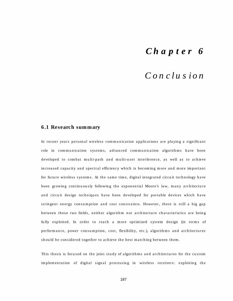
187
Chapter 6
Conc lus ion
6.1 Research summary
In recent years personal wireless communication applications are playing a significant
role in communication systems, advanced communication algorithms have been
developed to combat multi-path and multi-user interference, as well as to achieve
increased capacity and spectral efficiency which is becoming more and more important
for future wireless systems. At the same time, digital integrated circuit technology have
been growing continuously following the exponential Moore’s law, many architecture
and circuit design techniques have been developed for portable devices which have
stringent energy consumption and cost constraints. However, there is still a big gap
between these two fields, neither algorithm nor architecture characteristics are being
fully exploited. In order to reach a more optimized system design (in terms of
performance, power consumption, cost, flexibility, etc.), algorithms and architectures
should be considered together to achieve the best matching between them.
This thesis is focused on the joint study of algorithms and architectures for the custom
implementation of digital signal processing in wireless receivers: exploiting the

188
interactions between the two to derive efficient solutions and thereby bridging the gap
between system and circuit level design. An architecture design and evaluation
framework is established and high-level implementation estimation and evaluation is
used to assist systematic architecture explorations and give feedback to algorithm
development and architecture optimization.
This methodology enables the development team to study the performance of candidate
algorithms at the system level and at the same time design an architecture that
matches the computational requirements of the algorithm, in order to minimize
implementation cost and power consumption. The advantages of bringing together
system and algorithm design, architecture design, and implementation technology are
demonstrated by example designs of wireless communications systems at both block
level and system level: multi-user detection for CDMA system, multiple antenna
processing, OFDM system, and multi-carrier multi-antenna system.
Design examples all show that multiple orders of magnitude gain in both energy and
area (cost) efficiency can be obtained by using dedicated hardwired and highly parallel
architectures (achieving 1000 MOPS/mW and 10000 MOPS/mm2) compared to running
software on DSP and other common signal processing solutions. It is also demonstrated
that efficiency and flexibility can be both achieved by combining the system design,
which identifies a constrained set of flexible parameters to reduce the associated
overhead, and an architectural implementation, which exploits the algorithm’s
structure and modularity to provide the desired flexibility.
Based on the results of this thesis, the common approach presently pursued by many
design teams, which is to separate the theory and system groups developing algorithms
from DSP and VLSI groups implementing them, should be abandoned in favor of a more
interdisciplinary design procedure, which enables systematic exploration of the
interrelations between the application, the required algorithms, the underlying

189
hardware architectures, and the technology based upon which the system is to be
realized.
6.2 Future work
There are a number of additional activities that could extend the results of this
research.
Design methodology: The design methodology presented in this thesis is the front-end
digital algorithm and architecture design and exploration part of a larger research effort
of developing a unified design environment for high-performance, low-power, and
flexible implementation of future wireless communications systems. Other parts include
analog design and back-end flow. The integration of all the components needs to be
demonstrated and the usefulness of such a design approach remains to be tested over
more designs.
Architectures: An architecture design generally makes trade-off between efficiency and
flexibility. By utilizing the features of the application domain and the properties of
digital signal processing algorithms, architectures can be designed to achieve both.
Low-power architecture design is also linked to the underlying CMOS technology
through parameters such as transistor switching speed, threshold, leakage current,
interconnect capacitance, etc. With ever-evolving application and the continuous
advances in signal processing techniques and CMOS technology, architecture design
efforts should be made correspondingly in order to optimize design metrics.
MCMA system design framework: An extensive design effort has to be made in order to
complete the system design, fabricate and test the digital baseband processing chip,
combine the baseband chip with multi-antenna analog front-end, measure the end-to-
end wireless link performance under real channel conditions. The completion of the

190
whole system will provide useful data for future research and wideband signal
measurements will be extremely helpful in the design of next-generation high-
performance systems and algorithms.
DSP block designs: One of the primary goals of kernel block designs is reusability. A
more formal methodology to support design reuse among a group of designers needs to
be developed, which should define the interface and documentation strategies and
facilitate design knowledge encapsulation from generation to generation. The usefulness
of the high-level block library for digital communications systems grows with its
expansion. In addition, the library management strategies, such as version control and
technology migration, are needed to successfully apply the design methodology
presented in this thesis.
191
Appendix A
High -Leve l B l o ck L ib rary f o r Commun icat ions Sys tems
A.1 Introduction
The methodology proposed in Chapter 2 is applied for design exploration when building
signal processing blocks, as examples given in Chapter 3. When putting many blocks
together to make a system, it is desired to explore at higher level with larger granularity
due to the increased complexity. For system design, building each block from fine-grain
elements can be avoided by providing a high-level block library. This approach is
especially feasible for communications systems, which are dominated by a few
commonly used, parameterized, and computational (data-path) intensive DSP kernels.
This appendix summarizes the designs of some major blocks, with the focus on
architectures and hardware implementation. For each block, the discussion includes
functionality description, fixed-point arithmetic, possible architectures, and
parameterized Simulink implementation.
192
A.2 CORDIC
CORDIC (COordinate Rotation Digital Computer algorithm) block is commonly used for
the computation of trigonometric hyperbolic functions, coordinate transformations,
rotation of complex valued phasors, multiplication, and division. It calculates all the
desired functions iteratively in a rather simple and elegant way. An overview and
detailed discussion of CORDIC algorithm and architectures can be found in [Dawid99].
A.2.1 Functionality The basic idea underlying the CORDIC scheme is to carry out a vector rotation by an
arbitrary angle θ via a series of b+1 “micro-rotations” using a fixed set of predefined
elementary angles αi, i.e.,
1,1,0
+−∈σασ=θ ∑=
i
b
iii
and
,...,2,1,0,2arctan biidef
i ==α − .
It follows that a micro-rotation can be realized via two simple shift and add/subtract
operations:
⋅
σ−σ
+=
⋅
ασ−
ασ
α+=
−
−
−
+
+
i
ii
i
ii
i
i
i
ii
ii
ii
i
yx
yx
yx
1221
211
1tantan1
tan11
2
21
1
.

193
And the final result with a precision of b bits is obtained after the execution of b+1
“micro-rotations” and a multiplication with a constant scaling factor ∏=
−+=
b
ii
S0
2211
.
S can also be decomposed into a sequence of simple shift and add/subtract operations
as a series of additional scaling iterations.
CORDIC has two modes of operation: vectoring and rotation. Vectoring computes the
magnitude and phase of a vector or say the vector (x, y)T is rotated to the x-axis, i.e.,
in
inout
ininin
out
out
xy
yxxsignyx
arctan
0)( 22
=θ
+⋅=
,
and for each micro-rotation step, outiii ysignxsign σ=⋅=σ )()( .
Rotation rotates the vector (x, y)T by angle θin, i.e.,
inout
in
in
inin
inin
out
out
yx
yx
θ=θ
⋅
θθ−θθ
=
cossinsincos
,
with ini σ=σ .
A.2.2 Architectures A number of architectures can be used for the hardware implementation of CORDIC, as
categorized below. The choice is a trade-off between area, throughput, latency, and
power consumption, depending on the application requirements.

194
• Recursive architecture: only has one CORDIC processing unit with k stages and
k < n (= the total number of stages). This unit is basically composed of 2k
variable shifter, 2k add/subtract units (which performs addition or subtraction
according to a control signal) and two registers. The micro-rotation and scaling
stages are executed sequentially on this unit and it generates a final result every
kn / cycles. The cycle period is roughly k times the critical path of an
add/subtract unit due to the fact that in vectoring mode the control signal iσ is
determined by the MSB’s of the results from the previous stage. If only rotation
mode is needed and the generation of the control signals is not in the critical
path, then the delay of k cascaded add/subtract units will be shorter.
• Array architecture: a fully parallel architecture (k = n), has dedicated processing
unit for each stage and generates a final result every cycle. The variable shifters
can be replaced by fixed shifters (i.e., wires). Consequently each stage is
composed of basically two add/subtract units. This architecture can be
pipelined by inserting two pipeline registers every j stages. j = 1 results in a fully
pipelined scheme which has the fastest throughput (the cycle period is
determined by the critical path of an add/subtract unit), while j = n results in an
un-pipelined version with the cycle period determined by the critical path of n
concatenated add/subtract units.
Clearly, an add/subtract unit is the key building element of CORDIC. Various adder
types can be chosen to meet performance, area, and power consumption requirements.
A.2.3 Simulink model The structure of a CORDIC block is very regular and modular with building elements of
shifter, add/subtract unit, and register, but a range of architectural parameters in
terms of the amount of pipelining and parallelism can be chosen as discussed above. A
Simulink model generator was developed in MATLAB to automatically generate a bit-
true (fixed-point) and cycle-accurate structural model according to the following
parameters:
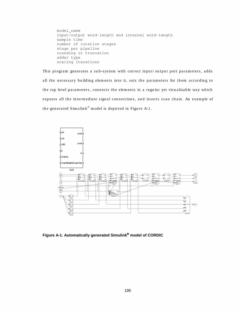
195
model_nameinput/output word-length and internal word-lengthsample timenumber of rotation stagesstage per pipelinerounding or truncationadder typescaling iterations
This program generates a sub-system with correct input/output port parameters, adds
all the necessary building elements into it, sets the parameters for them according to
the top level parameters, connects the elements in a regular yet visualizable way which
exposes all the intermediate signal connections, and inserts scan chain. An example of
the generated Simulink model is depicted in Figure A-1.
Figure A-1. Automatically generated Simulink model of CORDIC

196
A.3 FFT /IFFT
The FFT (Fast Fourier Transform)/IFFT (Inverse FFT) is a critical computational block
for OFDM systems (Section 5.2.1) and filter banks. An interesting feature of FFT/IFFT is
that IFFT can be performed using a FFT block by conjugating input and output of the
FFT and dividing the output by the FFT size. Hence the same hardware can be used for
both FFT and IFFT. In this section, the implementation of FFT is discussed, which can
be directly applied to IFFT implementation.
A.3.1 Functionality The digital computation of the N-point DFT (discrete Fourier transform) [Oppenheim89]
is expressed as
),0[][][1
0NkWnxkX
N
n
nkN ∈=∑
−
=
where the complex exponential coefficients are baja
b eWπ−
=2
.
A direct computation of the DFT formula (for all k) requires NN × multiplications and
)1( −× NN additions. FFT algorithms are more efficient implementations that reduce
the number of multiplication to NN 2log following a divide-and-conquer approach. The
basic idea is to divide a FFT of length N into two FFT’s half of the length, each of which
is then further divided to two FFT’s of quarter length. This process continues until the
FFT length is reduced to 2, which can be computed directly by a so-called “butterfly”
unit.
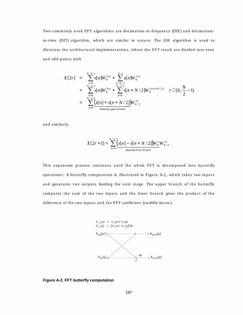
197
Two commonly used FFT algorithms are decimation-in-frequency (DIF) and decimation-
in-time (DIT) algorithm, which are similar in nature. The DIF algorithm is used to
illustrate the architectural implementations, where the FFT result are divided into even
and odd points with
( )
)12
,0[
]2/[][
]2/[][
][][]2[
12/
02/
12/
0
)2/(212/
0
2
1
2/
212/
0
2
−∈
++=
++=
+=
∑
∑∑
∑∑
−
=
−
=
+−
=
−
=
−
=
Nr
WNnxnx
WNnxWnx
WnxWnxrX
N
n
rnN
branchupperButterfly
N
n
NnrN
N
n
rnN
N
Nn
rnN
N
n
rnN
444 3444 21
and similarly,
( )∑−
=
+−=+12/
02/]2/[][]12[
N
n
rnN
branchlowerButterfly
nN WWNnxnxrX
4444 34444 21.
This expansion process continues until the whole FFT is decomposed into butterfly
operations. A butterfly computation is illustrated in Figure A-2, which takes two inputs
and generates two outputs feeding the next stage. The upper branch of the butterfly
computes the sum of the two inputs and the lower branch gives the product of the
difference of the two inputs and the FFT coefficient (twiddle factor).
( ) WqXpXqXqXpXpX
mmm
mmm
⋅−=+=
+
+
][][][][][][
1
1
] p [X m
] q [ X m
] p [ X 1 m +
]p[ X 1 m+-1
W
Figure A-2. FFT butterfly computation

198
A full expansion of a 16-point FFT is show in Figure A-3, which is composed of 32
butterfly computations. The outputs generated by DIF FFT are bit-reversed. For
example,
]5[]0101[]1010[]10[ 22 YYXX ===
where X is the FFT output and Y is the DIF computation output.
01W 11W 2
1W 31W 4
1W 51W 61W 71W
08W18W 28W38W
08W18W 28W38W
04W14W
04W14W
04W14W
04W14W
02W
02W
02W
02W
02W
02W
02W
02W
- 1 - 1 - 1
- 1 - 1 - 1
- 1
- 1
-1 -1 -1 -1
-1 -1 -1 -1
-1 -1
-1 -1
-1 -1
-1 -1
- 1
- 1
- 1
- 1
- 1
- 1
- 1
- 1
x[0] x[1] x[2] x[3] x[4] x[5] x[6] x[7] x[8] x[9] x[10] x[11] x[12] x[13] x[14] x[15]
X[0]X[8]X[4]X[12]X[2]X[10]X[6]X[14]X[1]X[9]X[5]X[13]X[3]X[11]X[7]X[15]
Figure A-3. Decimation-in-frequency 16-point FFT
A.3.2 Fixed-point arithmetic DSP functions like FFT are usually implemented in fixed-point arithmetic, where scaling
and overflow handling are crucial for correct behavior. The butterfly operation at each
stage of the FFT involves both complex addition and complex multiplication. Each
complex addition is composed of two real additions, which expand the input word-
length by 1 bit. Each complex multiplication is composed of four real multiplications
and two real additions. A real multiplication doubles the input word-length.

199
For a real addition, suppose the inputs a and b to the adder are two’s complement
numbers with word-length of M, i.e.
]12,2[b,a 1M1M −−∈ −−
The output
]0111,0010[]22,2[ 321K321KbitsMbitsM
MMba =−−∈+ .
Thus to ensure the correct behavior, the output word-length is either increased to M+1
bit or the output needs to be truncated or rounded to M bits. If truncation is performed,
the last bit of the output is simply discarded, which is equivalent to shift the output to
the right by 1 bit. If rounding is performed, a 1 will be added to the output first before
discarding the last bit. Rounding will not cause adder overflow since the biggest and
smallest numbers (a+b) have their last bit to be zero, after rounding the output will be
in the range same as that of a and b.
A complex multiplication is computed as
]DRe[]WIm[]DIm[]WRe[]XIm[]DIm[]WIm[]DRe[]WRe[]XRe[
⋅+⋅=⋅−⋅=
where W and D are the coefficient and data input and X is the output. Suppose both the
real and imaginary parts of W and D are of word-length M, and one of them, say D, is
not allowed to be the most negative number represented by M bits, i.e.,
]12,2(]12,2[
11
11
−−∈−−∈
−−
−−
MM
MM
DW
Then
200
]1010,0101[)2,2(],[]Im[],Re[1212
2222321K321K−−
−− =−=⋅⋅−∈MM
MMDWDWXX .
Note ]XRe[ and ]XIm[ can be represented by 2M-1 bits since the most significant two
bits of the 2M-bit representation are the same. Consequently, although the internal
values of the complex multiplier use word-length of 2M, the real and imaginary outputs
can be converted back to M bits without overflow, by taking the bits from position M-1
to 2M-2. Rounding cannot be used here unless saturation check is performed because it
may cause overflow.
It follows from the above analysis that the sufficient condition to ensure overflow-free
FFT computation (i.e., outputs remain inside the unit circle) is that all the FFT
coefficients and the data inputs have magnitudes less than or equal to unity. To
summarize, the fixed-point FFT computation requires:
• Fixed-point FFT coefficients are obtained by truncating floating-point FFT
coefficients towards zero to make sure those fixed-point coefficients have
magnitude less than or equal to 1.
• The inputs of an FFT are divided by 2 either through right-shift by 1 bit or
expanding the word-length by 1 bit to make sure the data inputs to the FFT are
inside the unit circle assuming both Re[x] and Im[x] are properly scaled to the
range of [-1, 1).
• The results of the addition or subtraction in a butterfly unit are either expanded
by 1 bit in word-length or right-shifted by 1 bit to avoid overflow. Rounding may
be used in conjunction with right-shift.
• The complex multiplication in a butterfly is performed at double the input word-
length M. The output is truncated to M-bit by taking the bits from M-1 to 2M-2.
A.3.3 Architectures The following sections summarize the commonly used architectures for FFT
implementation.

201
Processor approach This class of implementations has a single butterfly functional unit, so the design is
mainly focused on optimizing scheduling and memory access scheme. The Spiffee
processor [Baas99] is an example of using cached memory architecture to exploit the
regular memory access pattern of FFT algorithm in order to achieve low power
consumption. The processor can be programmed to perform any length of FFT, but
certain features, such as cache sizes, are optimized only for a certain FFT size. Without
much hardware duplication, this architecture is small in silicon area.
Fully parallel (direct mapped) approach In a fully parallel implementation, the signal flow graph is directly mapped into
hardware. For a 16-point FFT, there are total of 32 butterflies and they are
interconnected in the way as shown in Figure A-3. In general, N-point FFT needs
NN2log
2 butterfly units. This maximally parallel architecture has the potential for
highest performance or lowest power implementation with the cost of large silicon area
especially for large FFT sizes.
Column based approach In a column-based FFT architecture, the computations are re-arranged such that the
interconnections are kept the same in every stage as shown in Figure A-4. Since the
inputs to a butterfly are no longer needed once the outputs are computed, the outputs
can be routed to the inputs and the same butterflies can be used for the next stage (in-
place computation). As a result, only a single column of butterflies is needed which is
reused (time-multiplexed) by different stages. The FFT coefficients, however, need to be
changed from stage to stage. In general, N-point FFT needs 2N
butterfly units, 8
butterflies are needed for a 16-point FFT.

202
01W
11W
21W
31W
41W
51W
61W
71W
x[0] x[1] x[2] x[3] x[4] x[5] x[6] x[7] x[8] x[9] x[10] x[11] x[12] x[13] x[14] x[15]
08W
08W
18W
18W
28W
28W
38W
38W
04W
04W
04W
04W
14W
14W
14W
14W
02W
02W
02W
02W
02W
02W
02W
02W
X[0]X[1]X[2]X[3]X[4]X[5]X[6]X[7]X[8]X[9]X[10]X[11]X[12]X[13]X[14]X[15]
Single stage
Figure A-4. Column-based 16-point FFT
Pipelined approach In a pipelined architecture, only one butterfly unit is used for each stage, leading to
N2log as the total, compared to NN2log
2 in the fully-parallel approach and
2N
in
the column-based approach. The multiplier is separated from the butterfly to show the
hardware requirement distinctively. The usage of the butterfly unit is time-multiplexed
among the 2N
butterfly computations for each stage. Several pipelined architectures
have been proposed and they are summarized as following:
• Multi-path delay commutator (MDC) [Swartzlander84, 92]: the input sequence is
broken into two or four (for radix-2 or radix-4 respectively) parallel data streams
flowing forward, with correct “distance” between data elements entering the
butterfly units achieved by inserting proper delays.
Radix-2 (N = 16)
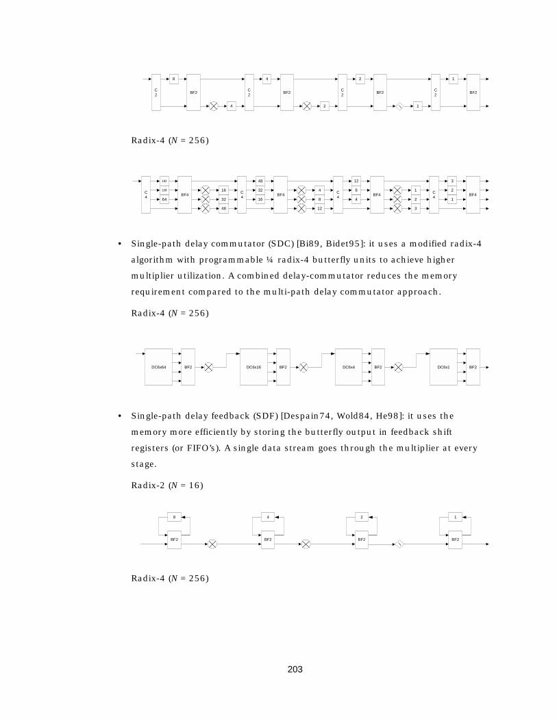
203
C2
8
BF2
4
C2
4
BF2
2
C2
2
BF2
1
C2
1
BF2
j
Radix-4 (N = 256)
C4
192
BF4
48
C4
48
BF4
12
C4
12
BF4 C4
3
BF4128
64 32
16 32
16 8
4 8
4
2
1
3
2
1
• Single-path delay commutator (SDC) [Bi89, Bidet95]: it uses a modified radix-4
algorithm with programmable ¼ radix-4 butterfly units to achieve higher
multiplier utilization. A combined delay-commutator reduces the memory
requirement compared to the multi-path delay commutator approach.
Radix-4 (N = 256)
DC6x64 BF2 BF2 BF2 BF2DC6x16 DC6x4 DC6x1
• Single-path delay feedback (SDF) [Despain74, Wold84, He98]: it uses the
memory more efficiently by storing the butterfly output in feedback shift
registers (or FIFO’s). A single data stream goes through the multiplier at every
stage.
Radix-2 (N = 16)
8
BF2
4
BF2
2
BF2
1
BF2j
Radix-4 (N = 256)
204
3x64
BF4
3x16
BF4
3x4
BF4
3x1
BF4
• Hybrid approach [Chang99]: it combines the benefit of both commutator and
feedback approach. The first stage uses feedback approach to save memory and
the rest of the stages use commutator approach for higher utilization.
The different approaches listed above have distinctive merits. The delay-feedback
approaches are more efficient in terms of memory utilization since the outputs of the
butterfly units can be directly used by the multipliers. Radix-4 algorithm based single-
path architectures have higher multiplier utilization, however, radix-2 algorithm based
architectures have simpler butterfly units which are better utilized. Table A-1 compares
the hardware requirements of the above architectures in terms of complex multipliers,
adders, memory size and control complexity.
Complex Multiplier Complex Adder
number utilization number utilization
Memory Size
(complex word)
Control Complexity
MDC (radix-2)
2(log4N-1) 50% 4log4N 50% 3N/2-2 simple
MDC (radix-4)
3(log4N-1) 25% 8log4N 25% 5N/2-4 simple
SDC (radix-4)
log4N-1 75% 3log4N 100% 2N-2 complex
SDF (radix-2)
2(log4N-1) 50% 4log4N 50% N-1 simple
SDF (radix-4)
log4N-1 75% 8log4N 25% N-1 medium
SDF (radix-22)*
log4N-1 75% 4log4N 50% N-1 simple
* Defined in Section 4.5.1
Table A-1. Hardware requirement comparisons of FFT architectures

205
Other architectural choices Other common architectural choices include:
• Radix: radix-2, radix-4 or radix-8 algorithms are typically used. Higher radix
implementation reduces the number of multiplications at the cost of more
complicated design of the butterfly unit.
• Arithmetic: digit-serial arithmetic [Chang99] can be used instead of word-
parallel arithmetic.
• Systolic-array architectures can be applied [Boriakoff94, Lim96].
• Complex Multiplier: since all the multiplications are actually rotations, CORDIC
block can be used [Despain74, Sarmiento98]. In addition, since all the twiddle
factors are known values, the micro-rotation schemes can be optimized and
stored in a ROM.
A.3.4 Simulink model A fixed-point FFT model was developed in C [Tang00]. The code was compiled using
MEX and linked into the Simulink as an s-function block. Figure A-5 shows the
Simulink block diagram and Table A-2 lists the parameters of the block.
Figure A-5. Simulink model of FFT
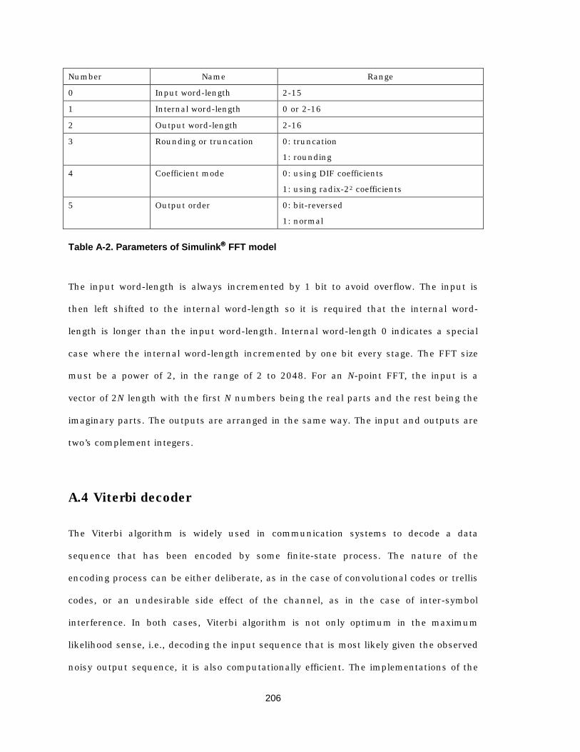
206
Number Name Range
0 Input word-length 2-15
1 Internal word-length 0 or 2-16
2 Output word-length 2-16
3 Rounding or truncation 0: truncation
1: rounding
4 Coefficient mode 0: using DIF coefficients
1: using radix-22 coefficients
5 Output order 0: bit-reversed
1: normal
Table A-2. Parameters of Simulink FFT model
The input word-length is always incremented by 1 bit to avoid overflow. The input is
then left shifted to the internal word-length so it is required that the internal word-
length is longer than the input word-length. Internal word-length 0 indicates a special
case where the internal word-length incremented by one bit every stage. The FFT size
must be a power of 2, in the range of 2 to 2048. For an N-point FFT, the input is a
vector of 2N length with the first N numbers being the real parts and the rest being the
imaginary parts. The outputs are arranged in the same way. The input and outputs are
two’s complement integers.
A.4 Viterbi decoder
The Viterbi algorithm is widely used in communication systems to decode a data
sequence that has been encoded by some finite-state process. The nature of the
encoding process can be either deliberate, as in the case of convolutional codes or trellis
codes, or an undesirable side effect of the channel, as in the case of inter-symbol
interference. In both cases, Viterbi algorithm is not only optimum in the maximum
likelihood sense, i.e., decoding the input sequence that is most likely given the observed
noisy output sequence, it is also computationally efficient. The implementations of the
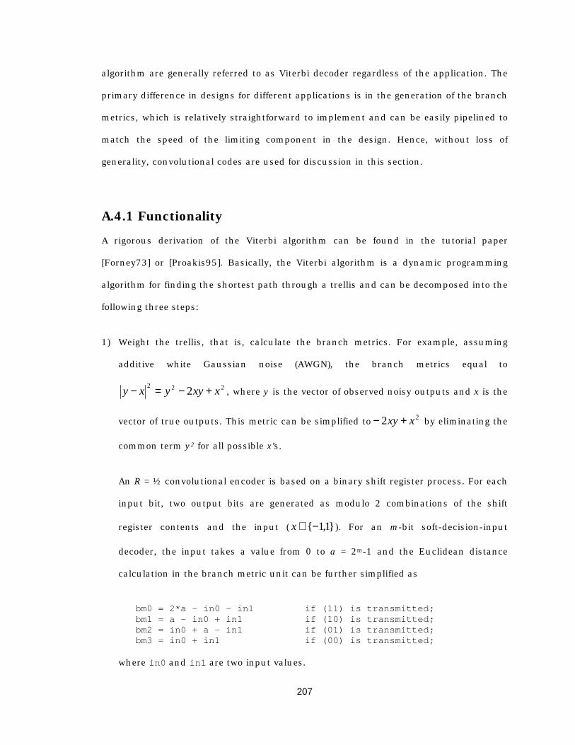
207
algorithm are generally referred to as Viterbi decoder regardless of the application. The
primary difference in designs for different applications is in the generation of the branch
metrics, which is relatively straightforward to implement and can be easily pipelined to
match the speed of the limiting component in the design. Hence, without loss of
generality, convolutional codes are used for discussion in this section.
A.4.1 Functionality A rigorous derivation of the Viterbi algorithm can be found in the tutorial paper
[Forney73] or [Proakis95]. Basically, the Viterbi algorithm is a dynamic programming
algorithm for finding the shortest path through a trellis and can be decomposed into the
following three steps:
1) Weight the trellis, that is, calculate the branch metrics. For example, assuming
additive white Gaussian noise (AWGN), the branch metrics equal to
222 2 xxyyxy +−=− , where y is the vector of observed noisy outputs and x is the
vector of true outputs. This metric can be simplified to 22 xxy +− by eliminating the
common term y2 for all possible x’s.
An R = ½ convolutional encoder is based on a binary shift register process. For each
input bit, two output bits are generated as modulo 2 combinations of the shift
register contents and the input ( 1,1−∈x ). For an m-bit soft-decision-input
decoder, the input takes a value from 0 to a = 2m-1 and the Euclidean distance
calculation in the branch metric unit can be further simplified as
bm0 = 2*a - in0 - in1 if (11) is transmitted;bm1 = a - in0 + in1 if (10) is transmitted;bm2 = in0 + a - in1 if (01) is transmitted;bm3 = in0 + in1 if (00) is transmitted;
where in0 and in1 are two input values.

208
2) Recursively compute the shortest paths to time n+1 in terms of the shortest paths to
time n. In this step, decisions are retained so that the recursively defined paths can
be reconstructed. This is called add-compare-select (ACS) recursion. The qualitative
interpretation is that the shortest path to state i at time n+1 must pass through a
predecessor state at time n by definition, and if the shortest path to i passes
through j, then the state metric for the path must be given by the state metrics for j
at time n plus the branch metric for the state transition from j to i. The final state
metric for i is given by the minimum of all candidate paths.
3) Reconstruct the shortest path using the decisions from step 2. The shortest path
leading to a state is referred to as the survivor path for that state and decode of the
trellis is referred to as survivor path decode. In theory, decoding of the shortest path
requires processing of the entire sequence. In practice, all the survivor paths merge
with high probability when trace back the trellis depth of L, at which point the
traced path is unique and can be decoded, independent of the starting state and
independent of any future ACS iterations. L is referred to as the survivor path
length, which is typically chosen to be 5 times the memory length of the encoder for
R=1/2 convolutional codes without puncturing [Proakis95]. If the decision of the
most likely current state (minimum state metric) is used, either to retrieve the
decoded output as in the register-exchange method or to start tracing back as in the
trace-back method, the survivor path length can be halved without affecting
performance and this scheme is referred to as best state decoding.
The signal flow of the Viterbi algorithm can be described by a trellis graph, which
contains N = 2K-1 states at any time with the constraint length of K. Figure A-6 depicts
two forms of the trellis graph, constant geometry and in-place, where the vertices of the
trellis are states and the edge weights are given by branch metrics.

209
Corresponding to the three steps listed above, there are three functional blocks in a
Viterbi decoder: branch metric unit which calculates the distances between the noisy
inputs and ideal symbols, state metric update unit which does the ACS recursion, and
survivor path decode unit which keeps track of the path through trellis. The ACS
recursion typically determines the achievable throughput. For high-speed Viterbi
decoder, block-based approaches are used to achieve higher concurrency and hence
throughput. Proposed techniques of block-based decoding are: state initialization,
interleaving, minimized method [Fettweis90], and sliding block decoder [Black97].
Stage 1 Stage 2 Stage 3 Stage 4 Stage 5
20
468
1012141357911 13 15
10
23456789
101112131415
10
23456789
10 11 12 13 14 15
10
2345678910 11 12 13 14 15
(a) (b)
10
23456789
10 11 12 13 14 15
40
812 15913 2610 14 37
11 15
80
192
10 3
11 4
12 5
13 6
14 7
15
Figure A-6. Viterbi trellis graph with constraint length of 5: (a) constant geometry, (b) in-place
A.4.2 Fixed-point arithmetic The recursive state metric update results in unbounded word-length growth due to the
addition of nonnegative branch metrics. There are several commonly used approaches
to deal with this problem as listed below, most of them (except the first one) attempt to
exploit the fact that despite the potential unbounded magnitude of survivor metrics, the

210
differences between them remain bounded by a fixed quantity that is independent of the
number of ACS recursion iterations.
• Reset: periodically reset the encoder to a “ground” state, or say, redundancy is
introduced into the channel input sequence to force the survivor sequences to
merge after some number of ACS recursions. The precision required in the ACS
depends on the reset period.
• Difference metric ACS: the Viterbi algorithm is reformulated to keep track only of
the differences between metrics for each pair of states.
• Variable shift: after some fixed number of recursions, the minimum survivor
metric is subtracted from all of the survivor metrics.
• Fixed shift: when all survivor metrics become negative (or positive), the survivor
metrics are shifted up (or down) by a fixed amount.
• Modulo normalization: use two’s complement representation of branch and
survivor metrics and modular arithmetic for ACS operations. Modulo arithmetic
exploits the fact that the Viterbi algorithm inherently bounds the maximum
dynamic range of state metrics to be
max2max log λ⋅≤∆ N
where N is the number of states and λmax = 2*a is the maximum branch metric
for radix-2 trellis. Given two numbers a and b such that |a-b| < c, the
comparison between them can be evaluated as (a-b) mod 2c. Hence, the state
metrics can be updated and compared mod 2∆max. By appropriately choosing the
state metric precision, the modulo arithmetic is implicitly implemented by
ignoring the state metric overflow. The required state metric word-length is twice
the maximum dynamic range of the updated state metrics just before the
compare state and is given by
1))((loglog max22 +λ⋅+ rN bits,
where the term r*λmax accounts for the potential dynamic range increase from
the input of a radix-2r ACS to the input of the compare stage due to the branch
metric addition. In the ACS unit, the comparison result is obtained by the most
significant sum bit from a subtractor. This excludes the option of using carry-
save format internally.

211
A.4.3 Architectures There are two major blocks in a Viterbi decoder: state metric update which updates N
state metrics per stage and survivor path decode which stores the survivors and selects
the maximum likelihood sequence. Their architectural choices are summarized below:
A.4.3.1 State metric update The similarity between shift register process trellis and FFT flow graph has been
exploited to generate architectures and schedules for ACS state metric update, and a
unified approach was proposed in [Black92a]. Similar to the FFT architectures, the
main classes of architectures are:
• Processor approach: This class of implementations has a single ACS unit, so the
design is mainly focused on scheduling and memory access optimizations.
• Parallel approach (= column based approach): The parallel architecture directly
maps the constant-geometry trellis graph into hardware. For large N’s, the global
interconnects can become a problem and since this architecture scales with N,
which exponentially grows with the constraint length K, it is not suitable for
implementations that require flexible constraint length.
• Pipelined and parallel-pipelined approach [Jia99 and Section 4.5.2.1]: In the
pipelined architecture, the property of Viterbi algorithm that the state order
returns to natural order after log2N stages of in-place computation (see (b) in
Figure A-6) is utilized. In this scheme, the data is processed between stages in a
single path and feedback is used to store new inputs and intermediate results.
The parallel-pipelined approach is an extension of the pipelined approach, where
M process elements are put in parallel and a shuffle-exchange network is
implemented for the last log2M stages. Figure A-7 depicts the block diagrams of
the three architectures.

212
4 2 1
4 2 1
4 2 1
4 2 1
4 2 1
4 2 1
4 2 1
4 2 1
Two-way radix-2 ACS
FIFO of length N Radix-2 ACS
N
32 16 8 4 2 1
10
23456789
10 11 12 13 14 15
10
23456789
10 11 12 13 14 15
(a)
(b)
(c)
Figure A-7. Architectures for state metric update unit: (a) parallel (constraint length = 5), (b) pipelined (constraint length = 7), (c) parallel-pipelined with M = 8 (constraint length = 7)
Other architectural choices: • Radix: With look-ahead operation, higher radix can be used in the branch metric
calculation and ACS unit to speed up at the cost of increased complexity. A summary of
the potential speedup and complexity increase as a function of trellis radix is given in
Table A-3. In practice, the ideal speedups cannot be achieved due to the additional delay
overhead associated with the exponentially increasing number of inputs to the compare
operation. Similarly, the complexity increases in the table are also conservative. For
example, a 4-input comparator, implemented as a hierarchy of 2-input comparators, is
three times the complexity of a 2-input comparator. Hence, the relative area efficiencies
given in the table are upper bounds for what can be achieved in practice. In a 0.25 µm
technology, the speed gain by using a radix-4 approach is only about a factor of 1.4 with
area overhead about a factor of 2.7.

213
Radix Ideal Speedup Complexity Increase Area Efficiency
2 1 1 1
4 2 2 1
8 3 4 0.75
16 4 8 0.5
Table A-3. Radix-2k speed and complexity measures of ACS unit
• ACS or CSA: By re-arranging the pipelining scheme, CSA (compare-select-add)
[Conway99] can be used instead of ACS, which can speed up the recursion loop.
• Internal number representation: Since the only outputs to other blocks are
decision bits, state metrics can be kept in carry-save format internally.
• Arithmetic: digit-serial arithmetic [Yeung95] can be used instead of word-parallel
arithmetic.
A.4.3.2 Survivor path decode Two major approaches for survivor path storage and decode are the register-exchange
method and the trace-back method [Black93]. Register-exchange is suitable for small
trellises (4 to 8 states) and is high in throughput. Trace-back is preferable for larger
trellises to reduce area and power dissipation.
• Register-exchange method: Associated with every trellis state is a register that
contains the survivor path leading to that state. Each survivor path is uniquely
specified by and stored as the decision sequence along the survivor path. The
current state decision is used to select the predecessor state decision sequence,
which is left shifted to allow the current decision to be appended to the
sequence. This update occurs concurrently for all the states and each update
corresponds to an exchange of the register contents along with shift and
appending operation, hence the name register-exchange. The interconnect
structure of the register-exchange method is equivalent to the trellis diagram.
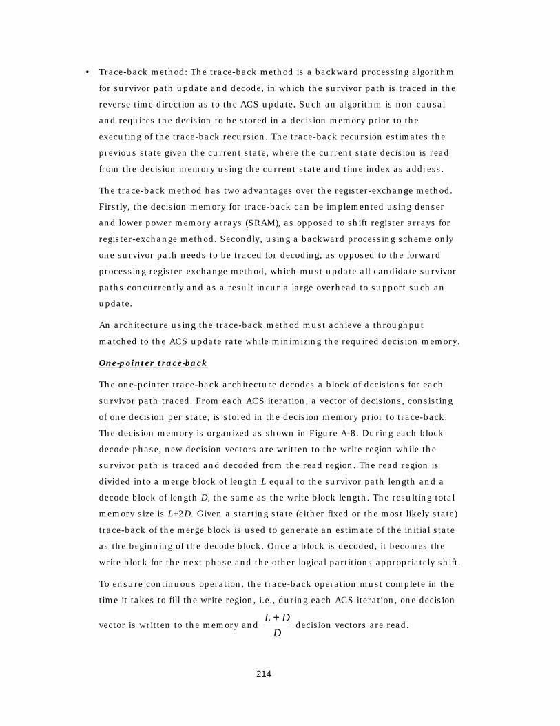
214
• Trace-back method: The trace-back method is a backward processing algorithm
for survivor path update and decode, in which the survivor path is traced in the
reverse time direction as to the ACS update. Such an algorithm is non-causal
and requires the decision to be stored in a decision memory prior to the
executing of the trace-back recursion. The trace-back recursion estimates the
previous state given the current state, where the current state decision is read
from the decision memory using the current state and time index as address.
The trace-back method has two advantages over the register-exchange method.
Firstly, the decision memory for trace-back can be implemented using denser
and lower power memory arrays (SRAM), as opposed to shift register arrays for
register-exchange method. Secondly, using a backward processing scheme only
one survivor path needs to be traced for decoding, as opposed to the forward
processing register-exchange method, which must update all candidate survivor
paths concurrently and as a result incur a large overhead to support such an
update.
An architecture using the trace-back method must achieve a throughput
matched to the ACS update rate while minimizing the required decision memory.
One-pointer trace-back
The one-pointer trace-back architecture decodes a block of decisions for each
survivor path traced. From each ACS iteration, a vector of decisions, consisting
of one decision per state, is stored in the decision memory prior to trace-back.
The decision memory is organized as shown in Figure A-8. During each block
decode phase, new decision vectors are written to the write region while the
survivor path is traced and decoded from the read region. The read region is
divided into a merge block of length L equal to the survivor path length and a
decode block of length D, the same as the write block length. The resulting total
memory size is L+2D. Given a starting state (either fixed or the most likely state)
trace-back of the merge block is used to generate an estimate of the initial state
as the beginning of the decode block. Once a block is decoded, it becomes the
write block for the next phase and the other logical partitions appropriately shift.
To ensure continuous operation, the trace-back operation must complete in the
time it takes to fill the write region, i.e., during each ACS iteration, one decision
vector is written to the memory and D
DL + decision vectors are read.
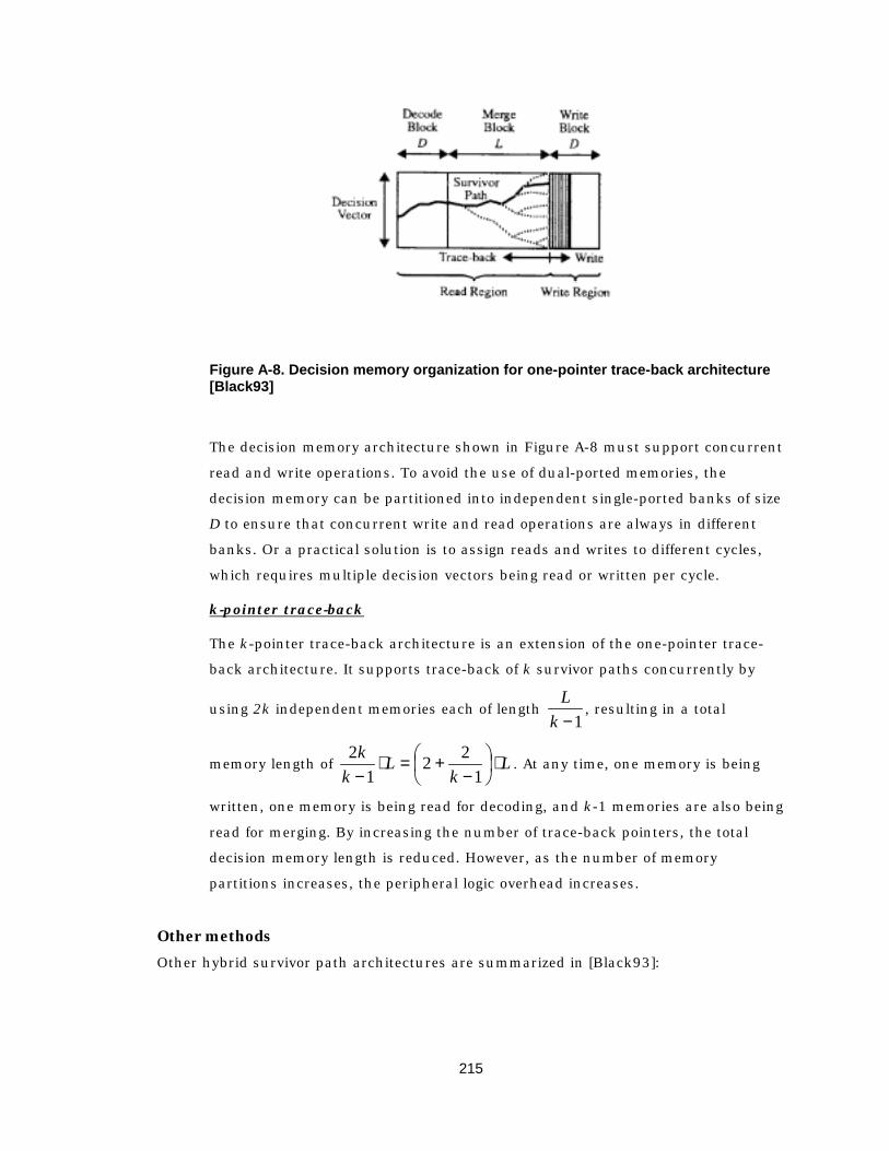
215
Figure A-8. Decision memory organization for one-pointer trace-back architecture [Black93]
The decision memory architecture shown in Figure A-8 must support concurrent
read and write operations. To avoid the use of dual-ported memories, the
decision memory can be partitioned into independent single-ported banks of size
D to ensure that concurrent write and read operations are always in different
banks. Or a practical solution is to assign reads and writes to different cycles,
which requires multiple decision vectors being read or written per cycle.
k-pointer trace-back
The k-pointer trace-back architecture is an extension of the one-pointer trace-
back architecture. It supports trace-back of k survivor paths concurrently by
using 2k independent memories each of length 1−k
L, resulting in a total
memory length of Lk
Lk
k ⋅
−+=⋅
− 122
12
. At any time, one memory is being
written, one memory is being read for decoding, and k-1 memories are also being
read for merging. By increasing the number of trace-back pointers, the total
decision memory length is reduced. However, as the number of memory
partitions increases, the peripheral logic overhead increases.
Other methods Other hybrid survivor path architectures are summarized in [Black93]:

216
• Trace-forward method: an alternative formulation of the register-exchange
method and can be described as a forward processing version of the trace-
back method.
• Hybrid pretrace-back architecture: apply look-ahead computation to the
trace-back recursion. The look-ahead (or pretrace-back) computation can be
implemented using a register-exchange network.
• Hybrid trace-forward architecture: combine trace-forward and trace-back
methods.
A.4.4 Simulink model In order to model the bit-true and cycle-accurate behavior of the modulo arithmetic in
the ACS units and survivor path decode (trace-back method without searching for the
best state to start) and support all the block parameters listed below, an s-function
based on C code was implemented for Viterbi decoder, as depicted in Figure A-9.
Block parameters:
• Constraint length (the number of states in the decoder = 2(constraint length – 1))
• Code generators
• Trace back depth
• Soft input precision (together with constraint length determine word-length of
the ACS units using modulo arithmetic)
The Simulink model supports any values of the above parameters and they can be set
in the “block parameter mask”. Simulink provides a convolutional encoder block,
which has constraint length and code generator as parameters. Puncturing can be
added as a separate block after the encoder and eraser can be added before the
decoder.

217
Figure A-9. Simulink model of Viterbi decoder
A.5 QRD
The QRD (QR Decomposition) block can be used as a building element for
• Interference suppression and diversity combining for multi-antenna systems
• Multi-user detection for CDMA systems
• Recursive least squares filters
• Any algorithms requiring matrix inversion
A.5.1 Functionality
Given ZXYrrr
+= A , where A is a m by n ( nm ≥ ) matrix,
the generic QRD hardware core described in Chapter 3 can
218
• Solve Xr
to minimize 2
YXrr
−A
• Decompose A to an unitary and an upper triangular matrix
• Get A-1 (for m = n)
If used as a least-squares estimator, the goal is to minimize the sum of squared errors,
∑=
−i
n
T
iwiwnynd
1
2
][][][][min rr
r.
(A “forgetting factor” ( 10 ≤β<< ) is commonly used to exponentially weight the squared
errors to discount old data from the computation, in order to track under non-
stationary condition.) That is to determine the weight vector ][iwr , which minimizes the
norm of residual error vector ][][
]1[][][ iw
iy
yidie
T
T
r
rM
r
r
−= . Since the Euclidean vector norm
is invariant with respect to unitary (orthogonal) transformations Q, where QHQ = I, QR
decomposition is applied to transform the input data matrix Y[i] of size i by k into an
upper triangular matrix R[i]:
][0
][][][
][][ iwi
iviu
ieiH rr
rr
−
=
RQ .
From this it can be seen that the minimum norm condition for the residual error ][ier is
obtained when ][][][ iuiwi rr =R . Since the matrix R[i] is upper triangular, the weight
vector ][iwr may be obtained via back-substitution. ][iwr is a vector of length k, and i
should be at least k and typically is chosen to be about 2-5 times of k for good
convergence. R[i] and ][iur can be calculated recursively on a sample by sample basis
using QRD-RLS algorithms based on complex Givens rotations.

219
This algorithm can be easily extended to incorporate concurrent adaptation of K
independent data sources. Since they all operate with the same input data matrix Y[i],
the QR decomposition parts are the same and thus only needs to be performed once to
compute R[i]. This is equivalent to solving ][][][ iuiwi rr =R for different ][iwr with
different right-side vector ][iur .
A.5.2 Architectures The algorithm and architecture exploration is discussed in details in Section 3.3. The
signal flow graph of this block is depicted in Figure A-10, which can concurrently
generate results for K streams.
Y D
OUT
.Vec Rot
…
…
…
…
10
0
0
0
…
K
Figure A-10. Signal flow diagram of QRD-RLS block
There are four modes of operations depending on the input values, they are listed in
Table A-4.

220
Mode of operation
Y D OUT Adaptation
Training Received signal Known training sequence
Residual error Update
Data detection Received signal 0 Filter output Freeze
Decision-directed adaptation
Delayed received signal
Decision signal Residual error Update
Weight flushing Identity matrix I 0 Filter coefficients Freeze
Table A-4. Operation modes of QRD-RLS block
• Training mode: update the array once every symbol and the output can be used
as a convergence indicator.
• Data detection mode: by freezing the adaptation, i.e., disconnecting the feedback
loop of all the elements in the array, this block acts like a fixed filter with
coefficients W on the input data Y. By setting D = 0, the output becomes
WTyr− , i.e., the filtered results using the most updated weight vectors.
Decisions can be made on these outputs by going through demodulation and
possibly decoding.
• Decision-directed adaptation mode: the decisions made in the data detection
mode can then be used as reference signal D to update the weights in a
decision-directed mode. The received signal used for detection needs to be
applied as Y again. For continuous tracking of the weight coefficients with
decision feedback, this block operates alternately in data detection and decision-
directed adaptation mode.
• Weight flushing mode: instead of using this block to perform the filtering
directly, this block can output the weight vectors and then complex multiply-
accumulators can be used to compute WTyr . W can be obtained by setting Y = I
and D = 0, in this case, the output becomes IW0 − , i.e., the negated weight
coefficients appear at the output one after another.
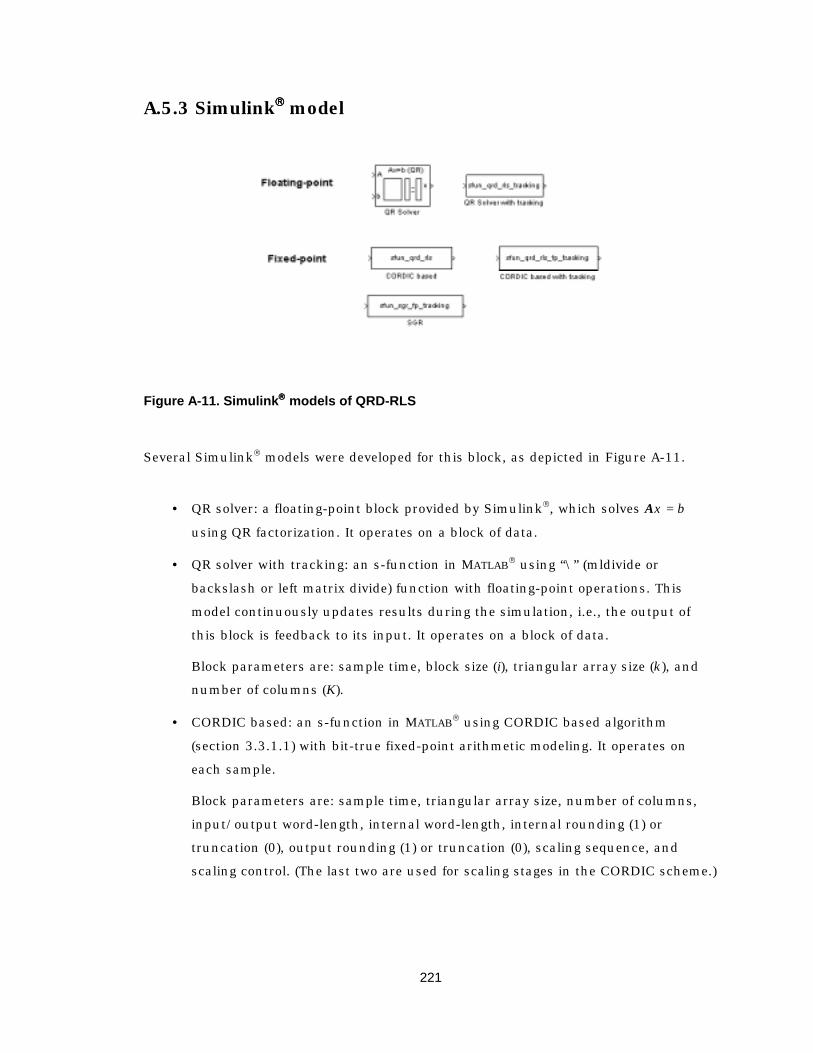
221
A.5.3 Simulink model
Figure A-11. Simulink models of QRD-RLS
Several Simulink models were developed for this block, as depicted in Figure A-11.
• QR solver: a floating-point block provided by Simulink, which solves Ax = b
using QR factorization. It operates on a block of data.
• QR solver with tracking: an s-function in MATLAB using “\” (mldivide or
backslash or left matrix divide) function with floating-point operations. This
model continuously updates results during the simulation, i.e., the output of
this block is feedback to its input. It operates on a block of data.
Block parameters are: sample time, block size (i), triangular array size (k), and
number of columns (K).
• CORDIC based: an s-function in MATLAB using CORDIC based algorithm
(section 3.3.1.1) with bit-true fixed-point arithmetic modeling. It operates on
each sample.
Block parameters are: sample time, triangular array size, number of columns,
input/output word-length, internal word-length, internal rounding (1) or
truncation (0), output rounding (1) or truncation (0), scaling sequence, and
scaling control. (The last two are used for scaling stages in the CORDIC scheme.)

222
• CORDIC based with tracking: an s-function in MATLAB using CORDIC based
algorithm, fixed-point operation, and continuously updating during the
simulation. It operates on each sample.
Block parameters are the same as those of CORDIC based block.
• SGR: an s-function in MATLAB using squared Givens rotation algorithm (Section
3.3.1.2), fixed-point operation, and continuously updating during the
simulation. It operates on each sample.
Block parameters are: sample time, triangular array size, number of columns,
input/output word-length, internal mantissa length, internal exponent length,
and rounding (1) or truncation (0).
A.6 FIR filter
FIR (Finite Impulse Response) filter is one of the most well-studied DSP blocks, the
designs of which can be found in numerous literatures.
A.6.1 Functionality FIR filtering is achieved by convolving the input data samples with the desired impulse
response of the filter. The output Y[n] of an N-tap FIR filter is given by the weighted sum
of the latest N input data samples:
∑−
=
−⋅=1
0]1[][
N
ii nXCnY ,
where the weights Ci are filter coefficients.
The fixed-point arithmetic and word-length optimization of FIR filter is also well-
studied. Tools have been developed to automatically translate a floating-point FIR filter
design to a fixed-point version given the SNR requirements. With feedback in an
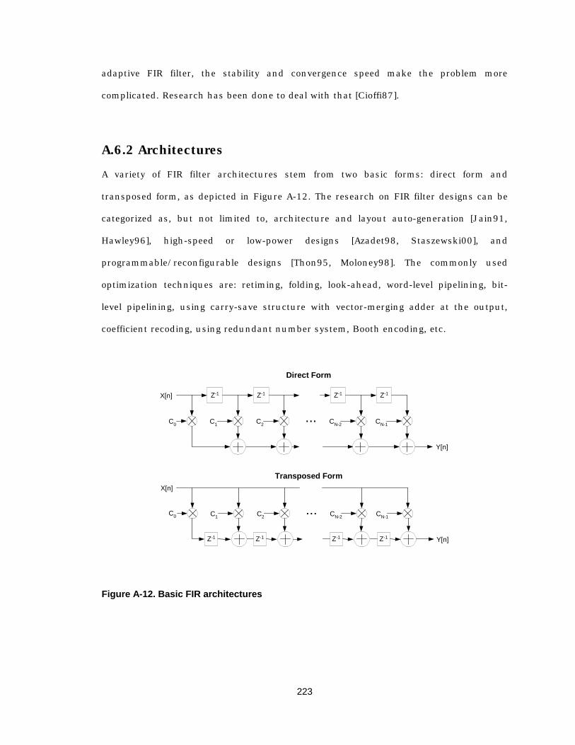
223
adaptive FIR filter, the stability and convergence speed make the problem more
complicated. Research has been done to deal with that [Cioffi87].
A.6.2 Architectures A variety of FIR filter architectures stem from two basic forms: direct form and
transposed form, as depicted in Figure A-12. The research on FIR filter designs can be
categorized as, but not limited to, architecture and layout auto-generation [Jain91,
Hawley96], high-speed or low-power designs [Azadet98, Staszewski00], and
programmable/reconfigurable designs [Thon95, Moloney98]. The commonly used
optimization techniques are: retiming, folding, look-ahead, word-level pipelining, bit-
level pipelining, using carry-save structure with vector-merging adder at the output,
coefficient recoding, using redundant number system, Booth encoding, etc.
Z-1 Z-1
...
Z-1 Z-1X[n]
Y[n]
C0 C1 C2 CN-1CN-2
Direct Form
...
X[n]
Y[n]
C1 C2 CN-1CN-2
Transposed Form
C0
Z-1Z-1 Z-1 Z-1
Figure A-12. Basic FIR architectures

224
A.6.3 Special cases There are several sub-families of FIR filter, commonly encountered in DSP systems, for
which special optimization techniques can be applied.
Fixed coefficient FIR filter If filter coefficients are fixed, the multiplication operations, which dominate area and
power consumption, can be replaced by shifts (= wirings) and additions/subtractions.
This can result in great savings in hardware implementation. There are tools to search
for the coefficient set that requires the least number of additions/subtractions, given
the specifications of the filter.
A special case in this family is sliding-window correlator, which is commonly used for
searching or extracting a known pattern from a signal sequence, such as dispreading in
direct sequence spread spectrum systems and pilot symbol (preamble) assisted timing
synchronization as in a MCMA receiver described in Chapter 5. The basic low-power
design techniques can be used for this block are:
• Using binary codes (+1 or –1) so that multiplication and addition operation per
tap becomes addition and sign flip operation.
• Using sign-magnitude number representation instead of two’s complement
representation to avoid the sign flip operation, i.e., flipping each bit and adding
1 at the LSB which involves carry propagation, and reduce switching activity. An
implementation of this scheme was presented in [Stone95] and the power saving
was analyzed in [Chandrakasan95], which strongly depends on the statistic of
the input signal. That implementation splits the signal path into two parallel
paths that accumulate positive and negative values separately. But this requires
number conversions at both input and output unless other DSP blocks of the
system also use sign-magnitude arithmetic.

225
• Optimization of the adder tree (for the direct form FIR) exploits the property of
the correlating sequence, for example, maximal length pseudo-random
sequences generated by a linear feedback shift register, as presented in
[Garrett99]. It was reported that a bypass-adder tree configuration
asymptotically approached a 12% reduction in power over regular binary adder
tree for large filter sizes, both with shift registers implementing the delay line.
• Using a register file FIFO instead of shift registers to reduce the unnecessary
switching activity on delayed data line. However, a global bus must be connected
to each register. Consequently the power dissipation of a correlator using
register file strongly depends on the bus width. Minimizing the transition on this
bus, by using coding techniques such as the bus invert method, can reduce the
overall power consumption considerably. [Garrett99] reported a 40% power
reduction with a 16-bit bus and a 30% reduction with 6-bit.
With fully parallel, direct mapped architecture, the implementation cost in terms of
both area and power consumption of the sliding-window correlator grows linearly with
the correlation sequence length.
Dot product (Correlator) A dot product unit (correlator) is a FIR filter with output down-sampled, i.e., for a N-tap
filter, it only needs the result at a multiple of N sample times and results at other times
are not relevant. Consequently, the filter can be implemented simply as a MAC (multiply
and accumulator). The matched filter used for dispreading in a DS-CDMA system is an
example application of the correlator.
Adaptive LMS filter The adaptive LMS (least mean square) filter [Haykin96] is used in many systems such
as adaptive equalizing and MMSE interference suppression. The multi-user detector for
a DS-CDMA system discussed in Section 3.2 is an example of delayed LMS correlator.
Although this algorithm is relatively robust, due to the present of feedback loop, special

226
cares need to be taken to choose the step size and word-lengths, in order to ensure
stability and at the same time achieve fast convergence speed and small residual error.
With fixed-point implementation, the objective of determining the word-length of
building blocks is to reduce the hardware cost by using the minimum word-length while
maintaining the overall performance. The output SNR is used as a gauge of the system
performance. There are three steady state error sources of the LMS algorithm besides
the minimum mean square error produced by the optimum Wiener filter: input
quantization, excess mean square error, and fixed-point implementation.
Excess mean square error comes from the stochastic adaptation process, which
remains after nominal convergence. This is due to the practical realization of the
adaptation equation, where instantaneous values of stochastic processes are used
instead of their expectation values. The steady state excess mean square error can be
shown approximately proportional to step size µ. This could be understood intuitively:
when a small value is assigned to µ, the adaptation is slow, which is equivalent to
having a long “memory” in the LMS adaptation. Because of the large amount of data
used by the algorithm to estimate the gradient vector, the excess mean square error is
small, on the average. On the other hand, when µ is large, the adaptation is relatively
fast, but in this case, less data are used for the estimation, hence degrading
performance.
For fixed-point implementation, it was found [Caraiscos84] that the accumulated
quantization error has mean square value approximately inversely proportional to the
adaptation step size µ. Making µ very small, in order to reduce the excess mean square
error, may result in a considerable quantization error. However, a very large value of µ
will lead to early termination of the adaptation due to quantization, i.e., the algorithm
stops before convergence is obtained, which may result in a significantly larger mean
square error. It was also found that the quantization error can be combated if more bits

227
are used for the filter’s coefficients than for the data inputs. In practice, “gear shifting”
is commonly used as a method to compromise those conflicting requirements, where
large step size is used initially for fast convergence and small step size is used finally for
smaller error.
A.6.4 Simulink model
There are many MATLAB functions supporting FIR filter design and the fixed-point
block set in Simulink also has FIR filters.
A.7 Summary
This appendix reviews the block designs of a DSP kernel library for communications
systems, which enables system design exploration at higher level. The blocks presented
are the key building elements of the system design framework introduced in Chapter 5.
The high-level block library also encapsulates design knowledge and facilitates design
reuse.
Depending on the design specifications and metrics, a designer can choose from a wide
range of various architectural implementations of these kernel blocks as provided in
this appendix. The selection criteria are based on the trade-offs between performance
(throughput), area, and power consumption.
228
Re f e rences
[3G] 3G Partnership Program Web Page: http://www.3gpp.org.
[Azadet98] K. Azadet and C.J. Nicole, "Low-power equalizer architectures for high speed modems," IEEE Communications Magazine, vol.36, no.10, p.118-126, Oct. 1998.
[Baas99] B. M. Baas, “A low-power, high-performance, 1024-point FFT processor,” IEEE Journal of Solid-State Circuits, March 1999.
[Benes99] M. Benes, Design and Implementation of Communication and Switching Techniques for the Pleiades Family of Processors, Master Thesis, University of California Berkeley, 1999.
[BDTI] http://www.bdti.com
[Bi89] G. Bi and E. V. Jones, “A pipelined FFT processor for word-sequential data,” IEEE Trans. Acoust., Speech, Signal Processing, p. 1982-1985, Dec. 1989.
[Bidet95] E. Bidet, D. Castelain, C. Joanblanq, and P. Stenn, “A fast signle-chip implementation of 8192 complex point FFT,” IEEE J. Solid-State Circuits, p. 300-305, Mar. 1995.
[Black92a] P. J. Black and T. H. Meng, “A unified approach to the Viterbi algorithm state metric update for shift register processes,” Proceedings of ICASSP-92, p. 629-32.
[Black92b] P. J. Black and T. H. Meng, “A 140-Mb/s, 32-state, radix-4 Viterbi decoder,” IEEE Journal of Solid-State Circuits, vol.27, p.1877-85, Dec. 1992.
[Black93] P. J. Black and T. H. Meng, “Hybrid survivor path architectures for Viterbi decoders,” Proceedings of ICASSP-93, p.433-6.
[Black97] P.J. Black and T.H. Meng, "A 1-Gb/s, four-state, sliding block Viterbi decoder," IEEE Journal of Solid-State Circuits, vol.32, no.6, p.797-805, June 1997.
[Boriakoff94] V. Boriakoff, “FFT computation with systolic arrays, a new architecture,” IEEE Transactions on Circuits and Systems – II: Analog and Digital Processing, vol. 41, no. 4, p. 278-284, April 1994.
[Brodersen97] R. W. Brodersen, “The Network Computer and its Future,” Proc. of the IEEE International Solid State Circuits Conference, San Francisco, CA, 6-8 Feb. 1997.

229
[Burd01] T. D. Burd, “Energy-Efficient Processor System Design,” Ph.D. Dissertation, U. C. Berkley, 2001.
[Camera01] K. Camera, Master thesis, U. C. Berkeley, 2001.
[Caraiscos84] C. Caraiscos, B. Liu, “A Roundoff Error Analysis of the LMS Adaptive Algorithm,” IEEE Transactions on Acoustics, Speech, and Signal Processing, vol. 32, no. 1, p. 34-41, Feb. 1984.
[Castille99] K. Castille, “TMS320C6000 Power Consumption Summary,” Application Report SPRA486B, Texas Instruments, November 1999. (http://www-s.ti.com/sc/psheets/spra486b/spra486b.pdf)
[Chameleon] http://www.chameleonsystems.com
[Chandrakasan92] A.P. Chandrakasan, S. Sheng, R.W. Brodersen, " Low-power CMOS digital design," IEEE Journal of Solid-State Circuits, vol.27, no.4, April 1992.
[Chandrakasan95a] A. P. Chandrakasan, M. Potkonjak, R. Mehra, J. Rabaey, and R. W. Brodersen, “Optimizing power using transformations,” IEEE Transactions on Computer-Aided Design of Integrated Circuits and Systems, vol.14, (no.1), p.12-31, Jan. 1995.
[Chandrakasan95b] A.P. Chandrakasan and R.W. Brodersen, “Minimizing power cinsumption in digital CMOS circuit,” Proceedings of the IEEE, vol.83, no.4, p.498-523, April 1995.
[Chang99] Y. Chang and K. K. Parhi, “Efficient FFT implementation using digit-serial arithmetic,” Proc. IEEE Workshop on Signal Processing Systems, p. 645-653, October 1999.
[Cioffi87] J. M. Cioffi, “Limited-Precision Effects in Adaptive Filtering,” IEEE Transactions on Circuits and Systems, Vol. Cas-34, No. 7, July 1987.
[Chouly93] A. Chouly, A. Brajal and S. Jourdan, “Orthogonal multicarrier techniques applied to direct sequence spread spectrum CDMA systems,” Proc. Of IEEE GLOBECOM’93, p. 1723-1728, Nov. 1993.
[Conway99] T. Conway, "Implementation of high speed Viterbi detectors," Electronics Letters, vol.35, no.24, p.2089-2090, 25. Nov. 1999.
[Cormen90] T. H. Cormen, C. E. Leiserson and R. L. Rivest, Introduction to Algorithms, MIT Press, Cambridge, MA, 1990.
[Davis01] W. R. Davis, N. Zhang, Kevin Camera, et. al., “A Design Environment for High Throughput, Low Power Dedicated Signal Processing Systems,” Proc. Custom Integrated Circuits Conference 2001, San Diego, CA, May 2001.
[Dawid99] H. Dawid and H. Meyr, “CORDIC algorithms and architectures,” chapter 24, 1999.
[Despain74] A. M. Despain, “Fourier transform computer using CORDIC iterations,” IEEE Trans. Comput., p. 993-1001, Oct. 1974.

230
[Dohler91] R. Döhler, “Squared Givens Rotation,” IMA Journal of Numerical Analysis, Vol. 11, No. 1, p. 1–5, January 1991.
[Fazel93] K. Fazel and L. Papke, “On the performance of convolutionallly-coded CDMA/OFDM for mobile communication system,” Proc. Of IEEE PIMRC’93, p. 468-472, Sept. 1993.
[Fettweis90] G. Fettweis, H. Dawid and H. Meyr, “Minimized Method Viterbi Decoding: 600Mb/s per chip,” Proc. GLOBECOM 90, Vol. 3, p. 1712-1716, Dec. 1990.
[Forney73] G. D. Forney, Jr., “The Viterbi Algorithm,” Proc. IEEE, Vol. 61 No. 3, p. 268-278, Mar 1973.
[Foschini96] G. J. Foschini, “Layered space-time architecture for wireless communication in a fading environment when using multi-element antennas,” Bell Labs Technical Journal, p. 41-59, 1996.
[Foschini98] G. J. Foschini and M. J. Gans, “On Limits of Wireless Communications in a Fading Environment When Using Multiple Antennas,” Wireless Personal Communications, Volume 6, No. 3, March 1998.
[Garrett99] D. Garrett and M. Stan, “Low Power Parallel Pread-Spectrum Correlator,” IEEE proc. Circuits Devices Systems, Vol. 146, No. 4, August 1999.
[George99] V. George, H. Zhang, and J. Rabaey, "Design of a Low Energy FPGA", ISLPED 1999.
[Ghazal99] N. Ghazal, “Evaluation & Guidance in Processor Architecture Selection for DSP,” Ph.D. thesis, 1999.
[Godara97a] L. C. Godara, “Applications of Antenna Arrays to Mobile Communications, Part I: Performance Improvement, Feasibility, and System Considerations,” Proc. IEEE, Vol. 85, No. 7, p. 1031–1060, July 1997.
[Godara97b] L. C. Godara, “Applications of Antenna Arrays to Mobile Communications, Part II: Beam-Forming and Direction-of-Arrival Considerations,” Proc. IEEE, Vol. 85, No. 8, p. 1195–1245, August 1997.
[Golden99] G. D. Golden, G. J. Foschini, R. A. Valenzuela, P. W. Wolniansky, “Detection Algorithm and Initial Laboratory Results using the V-BLAST Space-Time Communication Architecture,” Electronics Letters, Vol. 35, No. 1, Jan. 7, 1999.
[Golub89] G. H. Golub and C. F. Van Loan, Matrix Computations, The Johns Hopkins University Press, 2nd Ed., 1989.
[Guerra96] L. M. Guerra, Behavioral Level Guidance Using Property-Based Design Characterization, Ph.D. Thesis, University of California Berkeley, 1996.
[Haller00] B. Haller, “Dedicated VLSI Architectures for Adaptive Interference Suppression in Wireless Communication Systems,” in Circuits and Systems for Wireless Communications (M. Helfenstein and G. S. Moschytz, Eds.), Kluwer Academic Publishers, 2000, Ch. 23, p. 289–315.

231
[Hawley96] R.A. Hawley, B.C. Wong, T. J. Lin, J. Laskowski, H. Samueli, "Design techniques for silicon compiler implementations of high-speed FIR digital filters," IEEE Journal of Solid-State Circuits, vol.31, no.5, p.656-667, May 1996.
[Haykin96] S. Haykin, Adaptive Filter Theory, Prentice Hill, New Jersey, 3rd Ed., 1996.
[He98] S. He and M. Torkelson, “Designing pipeline FFT prcessor for OFDM (de)modulation,” in Proc. 1998 URSI International Symposium on Signals, Systems, and Electronics. Conference, September 1998.
[Hennessy96] J. L. Hennessy and D. A. Patterson, Computer Architecture: a Quantitative Approach, Morgan Kaufman, 1996.
[Hu96] C. Hu, “Chapter 2: Device and Technology Impact on Low Power Electronics” of “Low Power Design Methodologies,” edited by J. Rabaey and M. Pedram, Kluwer Academic Publishers, 1996.
[Jain91] R. Jain, P.T. Yang, T. Yoshino, "FIRGEN: a computer-aided design system for high performance FIR filter integrated circuits," IEEE Transactions on Signal Processing, vol.39, no.7, p.1655-1668, July 1991.
[Jia99] L. Jia, Y. Gao, J. Isoaho, and H. Tenhunen, “Design of a super-pipelined Viterbi decoder,” Proceedings of ISCAS'99.
[Keutzer94] K. Keutzer and P. Vanbekbergen, “The Impact of CAD on the Design of Low Power Digital Circuits,” IEEE Symposium on Low Power Electronics, p. 42-45, 1994.
[Klein00] A. G. Klein, “The Hornet Radio Proposal: A Multicarrier, Mutluser, Multiantenna System Specification,” Master thesis, U. C. Berkeley, 2000.
[Landman96] P. Landman, R. Mehra, and J. Rabaey, “An Integrated CAD Environment for Low-Power Design,” IEEE Design and Test of Computers, Vol. 13, No. 2, p. 72–82, June 1996.
[Lee97] W. Lee, et al., “A 1-V Programmable DSP for Wireless Communications,” IEEE Journal of Solid-State Circuits, November, p. 1766-1777, 1997.
[Lightbody98] G. Lightbody, R. Woods, J. McCanny, R. Walke, Y. Hu, and D. Trainor, “Rapid Design of a Single Chip Adaptive Beamformer,” in Proc. IEEE Workshop on Signal Processing Systems SiPS ’98, Cambridge, MA, p. 285–294, October 8–10, 1998.
[Lightbogy99] G. Lightbody, R. L. Walke, R. Woods, and J. McCanny, “Novel Mapping of a Linear QR Architecture,” in Proc. IEEE International Conference on Acoustics, Speech and Signal Processing ICASSP ’99, Phoenix, AZ, Vol. 4, p. 1933–1936, March 15–19, 1999.
[Lim96] H. Lim and E. Swartzlander, “Efficient systolic arrays for FFT algorithms,” Proc. Asilomar Conference on Signals, Systems and Computers, p. 141-145, October 1996.

232
[Long89] G. Long, F. Ling, and J. Proakis, “The LMS Algorithm with Delayed Coefficient Adaptation,” IEEE Transactions on Acoustics, Speech, and Signal Processing, Vol. 37, No. 9, p. 1397-1405, Sept. 1989.
[Markovic00] D. Markovic, EE225c class project report (http://bwrc.eecs.berkeley.edu/People/Grad_Students/dejan/ee225c/ofdm.htm), 2000.
[Moloney98] D. Moloney, J. O'Brien, E. O'Rourke, and F. Brianti, "Low-power 200-Msps, area-efficient, five-tap programmable FIR filter," IEEE Journal of Solid-State Circuits, vol.33, no.7, p.1134-1138, July 1998.
[Nee00] R. van Nee and R. Prasad, OFDM for Wireless Multimedia Communications, Artech House Publishers, 2000.
[Oppenheim89] A. V. Oppenheim and R. W. Schafer, Discrete-Time Signal Processing, Prentice Hill, New Jersey, 1989.
[Parhi95] K. K. Parhi, “High-level algorithm and architecture transformations for DSP synthesis,” Journal of VLSI Signal Processing, vol.9, (no.1-2), p.121-43, Jan. 1995.
[Poon00] A. S. Poon, “An Adaptive Multi-Antenna Transceiver for Slowly Flat Fading Channels,” Master thesis, U. C. Berkeley, 2000.
[Press93] W. H. Press, S. A. Teukolsky, W. T. Vetterling, and B. P. Flannery, Numerical Recipes in C: The Art of Scientific Programming, Cambridge University Press, 2nd Ed., 1993. (http://www.ulib.org/webRoot/Books/Numerical_Recipes/)
[Proakis95] J. G. Proakis, Digital Communications, McGraw Hill, New York, 3rd Ed., 1995.
[Rabaey96] M. Rabaey and M. Pedram (Eds.), Low Power Design Methodologies, Kluwer Academic Publishers, 1996.
[Rabaey97] J. Rabaey, "Reconfigurable Computing: The Solution to Low Power Programmable DSP," Proceedings 1997 ICASSP Conference, Munich, April 1997.
[Rader96] C. M. Rader, “VLSI Systolic Arrays for Adaptive Nulling,” IEEE Signal Processing Magazine, Vol. 13, No. 4, p. 29–49, July 1996.
[Raghunathan98] A. Raghunathan, N. K. Jha, and S. Dey, High-Level Power Analysis and Optimization, Kluwer Academic Publishers, 1998.
[Sarmiento98] R. Sarmiento, F. Tobajas, et al, “A CORDIC processor for FFT computation and its implementation using Gallium Arsenide technology,” IEEE Transactions on VLSI systems, vol. 6, no. 1, p. 18-30, March 1998.
[Staszewski00] R. B. Staszewski, K. Muhammad, and P. Balsara, "A 550-MSample/s 8-Tap FIR Digital Filter for Magnetic Recording Read Channels," IEEE Journal of Solid-State Circuits, vol. 35, no. 8, pp. 1205-1210, August 2000.
[Stimming01] C. Stimming, Project Report, May 2001.

233
[Stone95] K. M. Stone, “ Low Power Spread Spectrum Demodulator for Wireless Communications,” Master thesis, U. C. Berkeley, 1995.
[Swartzlander84] E. E. Swartzlander, W. K. W. Young, and S. J. Joseph, “A radix 4 delay commutator for fast Fourier transform processor implementation,” IEEE J. Solid-State Circuits, p. 702-709, Oct. 1984.
[Swartzlander92] E. E. Swartzlander, V. K. Jain, and H. Hikawa, “A radix 8 wafer scale FFT processor,” J. VLSI Signal Processing, p. 165-176, May 1992.
[Tang00] H. Tang, EE225c class project report, 2000.
[Tang01] H. Tang, “Indoor Wireless System Design,” PhD dissertation, U. C. Berkeley, 2001.
[Teuscher96] C. Teuscher, et al, “Design and Implementation Issues for a Wideband, Indoor, DS-CDMA System Pro-viding Multimedia Access,” Proceedings of the Thirty-Fourth Annual Allerton Conference, p. 623-632, Oct. 1996.
[Teuscher98] C. Teuscher, D. Yee, N. Zhang, and R. W. Brodersen, "Design of a Wideband Spread Spectrum Radio Using Adaptive Multiuser Detection," Proc. IEEE International Symposium on Circuits and Systems, Monterey, CA, May-June 1998.
[Thon95] L.E. Thon, P. Sutardja, F. S. Lai, and G. Coleman, "A 240 MHz 8-tap programmable FIR filter for disk-drive read channels," 1995 IEEE International Solid-State Circuits Conference. Digest of Technical Papers ISSCC '95, pp.82-3, 343, San Francisco, CA, USA, 15-17 Feb. 1995.
[TI] http://www.ti.com/sc/docs/products/dsp/c6000/index.htm
http://www.ti.com/sc/docs/products/dsp/c6000/benchmarks/index.htm
http://www.ti.com/sc/docs/products/dsp/c5000/bench.htm
http://www-s.ti.com/sc/psheets/spra071/spra071.pdf
http://www-s.ti.com/sc/psheets/spra486b/spra486b.pdf
[Tiwari96] V. Tiwari, S. Malik, A. Wolfe, and M. Lee, “Instruction Level Power Analysis and Optimization of Software,” Journal of VLSI Signal Processing, p. 1-18, 1996.
[Turner97] C. Turner, “Calculation of TMS320LC54x Power Dissipation,” Technical Application Report SPRA164, Texas Instruments, 1997.
[Xilinx] http://www.xilinx.com/products/logicore/fbl_dsp.htm
http://www.xilinx.com/products/logicore/tbl_comm_net.htm
http://www.xilinx.com/cgi-bin/powerweb.pl
[Verdu98] S. Verdu, Multiuser Detection, Cambridge University Press, Cambridge, UK, 1998.

234
[Wan00] M. Wan, H. Zhang, V. George, M. Benes, A. Abnous, V. Prabhu, J. Rabaey, "Design Methodology of a Low-Energy Reconfigurable Single-Chip DSP System," Journal of VLSI Signal Processing 2000.
[Weste98] N. Weste, and D. J. Skellern, “VLSI for OFDM,” IEEE Communications Magazine, p.127-31, vol.36, (no.10), Oct. 1998.
[Wold84] E. H. Wold and A. M. Despain, “Pipelined and parallel-pipeline FFT processors for VLSI implementation,” IEEE Trans. Comput., p. 414-426, May 1984.
[Wolniansky98] P. W. Wolniansky, G. J. Foschini, G. D. Golden, and R. A. Valenzuela, “V-blast: an architecture for realizing very high data rates over the rich-scattering wireless channel,” URSI International Symposium on Signals, Systems, and Electronics Conference Proceedings, p. 295-300, 1998.
[Yee93] N. Yee, J-P. Linnartz and G. Fettweis, “Multi-Carrier CDMA in Indoor Wireless Radio Networks,” Proc. Of IEEE PIMRC’93, p. 109-113, Sept. 1993.
[Yee01] D. G. Yee, “A Design Methodology for Highly-Integrated Low-Power Receivers for Wireless Communications,” PhD Dissertation, U. C. Berkeley, 2001.
[Yeung95] A.K. Yeung, J.M. Rabaey, "A 210 Mb/s radix-4 bit-level pipelined Viterbi decoder," 1995 IEEE International Solid-State Circuits Conference, Digest of Technical Papers, p.88-9, 344, San Francisco, CA, Feb. 1995.
[Zhang98a] N. Zhang, “Implementation Issues in the Design of a CDMA Baseband Receiver,” Master thesis, U. C. Berkeley, 1998.
[Zhang98b] N. Zhang, C. Teuscher, H. Lee, and R. W. Brodersen, "Architectural Implementation Issues in a Wideband Receiver Using Multiuser Detection," Proc. Allerton Conference on Communication Control and Computing, Urbana-Champaign, IL, September 1998.
[Zhang99a] H. Zhang, M. Wan, V. George, and J. Rabaey, “Interconnect Architecture Exploration for Low Energy Reconfigurable Single-Chip DSPs,” Proc. IEEE Computer Society Workshop on VLSI ’99, p. 2–8, Orlando, FL, April 8–9, 1999.
[Zhang99b] N. Zhang, A. Poon, D. Tse, R. W. Brodersen, and S. Verdu, "Trade-offs of Performance and Single Chip Implementation of Indoor Wireless Multi-Access Receivers," Proc. IEEE Wireless Communications and Networking Conference, September 1999.
[Zhang00a] N. Zhang, B. Haller and R. W. Brodersen, "Systematic Architecture Exploration for Implementing Interference Suppression Techniques in Wireless Receivers," Proc. IEEE Workshop on Signal Processing Systems, Lafayette, LA, October 2000.
[Zhang00b] N. Zhang and R. W. Brodersen, "Architectural Evaluation of Flexible Digital Signal Processing for Wireless Receivers," Proc. Asilomar Conference on Signals, Systems and Computers, Pacific Grove, CA, October 2000.