AIChE 2012 Presentation
58
Mass transport at internal interfaces of inorganic materials Kedarnath Kolluri, M. J. Demkowicz and B. Uberuaga Financial Support: Center for Materials at Irradiation and Mechanical Extremes (CMIME) at LANL, an Energy Frontier Research Center (EFRC) funded by U.S. Department of Energy, Office of Science, Office of Basic Energy Sciences Acknowledgments: R. G. Hoagland, J. P. Hirth, A. Kashinath, A. Vattré, X.-Y. Liu, A. Misra, and A. Caro
-
Upload
kedarnath-kolluri -
Category
Technology
-
view
55 -
download
0
Transcript of AIChE 2012 Presentation

Mass transport at internal interfaces of inorganic materials
Kedarnath Kolluri, M. J. Demkowicz and B. Uberuaga
Financial Support:
Center for Materials at Irradiation and Mechanical Extremes (CMIME) at LANL,
an Energy Frontier Research Center (EFRC) funded by
U.S. Department of Energy, Office of Science, Office of Basic Energy Sciences
Acknowledgments: R. G. Hoagland, J. P. Hirth, A. Kashinath, A. Vattré, X.-Y. Liu, A. Misra, and A. Caro

Internal interfaces enhance ionic conduction
trolyte material. So far, yttria-stabilized zirconia(Y2O3)x(ZrO2)1–x (YSZ) is the material mostlyused in SOFCs because of its mechanical sta-bility, chemical compatibility with electrodes, andhigh oxygen ionic conductivity. It is well knownthat doping ZrO2 with Y2O3 stabilizes the cubicfluorite structure of ZrO2 at room temperature andsupplies the oxygen vacancies responsible forthe ionic conduction, resulting in high valuesof the oxygen conductivity at high temperatures(5–7). Amaximumvalue of 0.1 S/cm (where 1 S =1 A/V) at 1000°C is observed for the 8 to 9 molepercent (mol %) yttria content (2–4). A severedrawback toward the final implementation ofSOFCs is the relatively low room temperatureionic conductivity of this material, which imposesrather high operational temperatures around 800°C(1–4). The search for alternative electrolytes hasnot yet been successful in reaching the conduc-tivity value of 0.01 S/cm desired for room tem-perature operation (1–4).
Only modest reductions in the operationtemperature of SOFCs (500° to 700°C) can beanticipated with the recently proposed optimizedelectrolytes such as gadolinia-doped ceria andlanthanum gallates (8–11). On the other hand, theone to two orders of magnitude increase of theelectrical conductivity reported (12–14) in nano-crystalline samples as compared with single crys-tals outlines the importance of processing as analternative route to increasing conductivity valuestoward the desired levels. Because modern thinfilm growth techniques allow a precise control oflayer thickness and morphology, they provide apathway for the production of solid electrolyteswith optimized properties. Maier et al. found asubstantial increase of the dc ionic conductivityof superlattices of CaF2 and BaF2 when thethickness of the individual layers was decreaseddown to 16 nm, assigned to a size effect due tothe space charge regions being smaller than thelayer thickness (15, 16). Kosacki et al. havereported enhanced conductivity in highly tex-tured thin films of YSZwith thicknesses between60 and 15 nm, reaching 0.6 S/cm at 800°C (17).Because reducing film thickness (and thereforeincreasing the fraction of material near the in-terface) produces such a noticeable conductivityenhancement, the interfaces themselves wouldseem to play a determining role in the outstand-ing conductivity properties observed.
To search for interface effects, we fabricatedheterostructures where YSZ layers (with 8 mol %nominal yttria content) in the thickness range from62 nm down to 1 nm were sandwiched betweentwo 10-nm-thick layers of insulating SrTiO3 (STO).Also, superlattices were grown, alternating 10-nm-
thick STO films with YSZ layers with thicknessbetween 62 and 1 nm (18). Figure 1A displays alow-magnification (inset) and a high-resolutionannular dark field (or Z-contrast) image of a[YSZ1nm/STO10nm]9 superlattice (with ninerepeats), showing the excellent crystalline qualityof the sample. The layers appear continuous andflat over long lateral distances (a few microns).The interfaces between the STO and the YSZare seen to be atomically flat. From the high-magnification image it is possible to count thenumber of unit cells of STO and YSZ, nomi-nally 25 of STO and 2 of YSZ. Most impor-tantly, the YSZ is perfectly coherent with theSTO, in agreement with x-ray diffraction (XRD)results (fig. S1), meaning that the ultrathin layerof YSZ grows rotated by 45° around the c axisand strains to match the STO lattice. Because thebulk lattice constants of STO and YSZ are
0.3905 (19) and 0.514 nm (20), respectively, theepitaxial growth of the YSZ on top of the STOensures a large, expansive strain in the thin YSZlayers of 7% in the ab plane. Increasing the thick-ness of YSZ (for constant STO thickness) resultsin a loss of structural coherence, as reflected by areduction of superlattice satellites in XRD. Elec-tron microscopy observations confirm that therelease of strain results in a granular morphology,although the growth remains textured.
We plotted the lateral electrical conductivity(real part s!) of the thinnest YSZ trilayer versusfrequency in a double logarithmic plot (Fig. 2).The characteristic electrical response of ionic con-ductors (21–23) is observed in the figure. The longrange or sdc ionic conductivity of the material isobtained from the plateau found in s! versusfrequency plots. In the presence of blocking effectsdue to grain boundaries or electrodes, a further
1Grupo de Física de Materiales Complejos, UniversidadComplutense de Madrid, Madrid 28040, Spain. 2MaterialsScience and Technology Division, Oak Ridge NationalLaboratory, Oak Ridge, TN 37831, USA. 3Escuela TécnicaSuperior de Ingenieros de Telecomunicaciones, Universi-dad Politécnica de Madrid, Madrid 28040, Spain.
*To whom correspondence should be addressed. E-mail:[email protected]
Fig. 1. (A) Z-contrast scanning transmission electron microscopy (STEM) image of the STO/YSZ interface ofthe [YSZ1nm/STO10nm]9 superlattice (with nine repeats), obtained in the VG Microscopes HB603Umicroscope. A yellow arrow marks the position of the YSZ layer. (Inset) Low-magnification image obtainedin the VGMicroscopes HB501UX column. In both cases a white arrow indicates the growth direction. (B) EELspectra showing the O K edge obtained from the STO unit cell at the interface plane (red circles) and 4.5 nminto the STO layer (black squares). (Inset) Ti L2,3 edges for the same positions, same color code. All spectraare the result of averaging four individual spectra at these positions, with an acquisition time of 3 s each.
Fig. 2. Real part of the lateralelectrical conductivity versus fre-quency of the trilayer with 1-nm-thick YSZ in a double log plot.Isotherms were measured in therange of 357 to 531 K. The solidline represents a NCL contribution(s! ~ Aw, where A is a temperature-dependent proportionality factorand w is the angular frequency),as explained in the text. Stars iden-tify the value of sdc. The uncertain-ty of conductance measurements is1 nS (10!2 S/cm in conductivity forthe sample shown, see error bar).(Inset) Imaginary versus real partof the impedance (Nyquist) plots at492, 511, and 531 K. Whereas thehigh-frequency contribution is a Debye-like process characterized by a conductivity exponent n = 0, the“grain boundary” term observed in the Nyquist plots shows a clear deviation from a Debye behavior, asreflected by the distorted impedance arcs.
www.sciencemag.org SCIENCE VOL 321 1 AUGUST 2008 677
REPORTS
on S
epte
mber
17, 2011
ww
w.s
cie
ncem
ag.o
rgD
ow
nlo
aded fro
m
decrease of s! (below bulk sdc values) may occurtoward lower frequencies. For clarity, the value ofsdc has been identified by using stars. The sdcvalue is found to be thermally activated, so whenthe temperature is reduced the conductivity curvesshift downwards in Fig. 2. The inset in Fig. 2displays Nyquist plots for the same sample. Todetermine the nature of the charge carriers, wemeasured the conductance of the samples bymeans of dc measurements. As can be observed infig. S2, the dc conductance (open circles) is threeto four orders of magnitude lower than the valuesobtained from ac measurements (solid squares) inthe entire temperature measurement range. Thisresult indicates that the electronic contribution tothe ac measurements can be considered negligi-ble, and thus, the measured ac transport isattributable to an ionic diffusion process.
In Fig. 3, the temperature dependence of thesdc of [STO10nm/YSZXnm/STO10nm] trilayers isshown together with data corresponding to a singlecrystal and the 700-nm thin film from (7). Whereasthe “bulklike” samples (the thin film and the singlecrystal) show the well-known Arrhenius behaviorwith an activation energy of ~1.1 eV, the trilayersshow much larger conductivity values and smallervalues of the activation energy. The thickest trilayer(62-nm YSZ) already shows an increase of abouttwo orders of magnitude in the high-temperature dcconductivity, and the dc activation energy decreasesto 0.72 eV. When decreasing the thickness of theYSZ layer to 30 nm, the dc conductivity increasesanother three orders of magnitude, and the activa-tion energy decreases to 0.6 eV. The high values ofthe pre-exponential factor of ~107 (ohm·cm)!1 arecomparable to those found in other ion conductors(24) [see supporting onlinematerial (SOM) text]. Ifthe thickness is further reduced all the way downto 1 nm (two unit cells of YSZ), the conductivityis observed to increase as the inverse of the YSZlayer thickness, but the conductance is essentiallythickness-independent (bottom inset in Fig. 3).We can think of three parallel conduction pathsdue to the interfaces and the bulk YSZ and STOlayers. The bulk conductivity of YSZ is 10!7 S/cmat 500 K, which would yield a conductance valueof ~10!14 S for 1-nm-thick layers. This value ismuch lower than the 10!6 S value measured withthe ac technique. If we instead assume that the highconductance (G = 10!6 S) is due to electronicconduction in the STO, both ac and dc techniqueswould provide this same value, contrary to what isobserved (fig. S2).Moreover, reported conductivityvalues in STO thin films (25) are also much lowerthan those necessary to explain the high conduct-ance observed. Because bulk YSZ or STO contri-butions can be ruled out, an interface conductionmechanism is inferred.
To further test this scenario, we grew super-lattices repeating the [YSZ1nm/STO10nm] growthunit. We found (top inset in Fig. 3) that con-ductance scales nowwith the number of interfacesup to a number of eight (four bilayer repetitions).There is a scaling breakdown in the figure, ob-served for a larger number of bilayer repetitions,
most likely resulting from disorder building up inthis highly strained structure. The experimentaldata indicates that the first STO/YSZ interfacedoes not contribute to the large ionic conductivityobserved in the samples, probably because the firstSTO layer is somehow different from the others asit is grown directly on the substrate. This scaling,together with the invariance of the conductancewith the thickness of the YSZ, shows that the largeconductivity values in these heterostructures orig-
inate truly at the interfaces between YSZ and STO.Our results indicate a superposition of two parallelcontributions—one due to the bulk and one at-tributable to the interface—and the colossal ionicconductivity is observed as long as the interfaceconductance is larger than that of the bulk. Theabrupt conductivity decrease when the thicknesschanges from 30 to 62 nm is most likely due to adegraded interface structure when the YSZ layersexceed the critical thickness.
Fig. 3. Dependence of the logarithm of thelong-range ionic conductivity of the trilayersSTO/YSZ/STO versus inverse temperature. Thethickness range of the YSZ layer is 1 to 62 nm.Also included are the data of a single crystal(sc) of YSZ and a thin film (tf) 700 nm thick[taken from (7)] with the same nominalcomposition. (Top inset) 400 K conductanceof [YSZ1nm/STO10nm](ni/2) superlattices as afunction of the number of interfaces, ni.(Bottom inset) Dependence of the conduct-ance of [STO10nm/YSZXnm/STO10nm] trilayers at500 K on YSZ layer thickness. Error bars areaccording to a 1 nS uncertainty of the con-ductance measurement.
Fig. 4. (A) EELS chemical maps. The ADF image in the upper panel shows the area used for EELSmapping(spectrum image, marked with a green rectangle) in the [YSZ1nm/STO10nm]9 superlattice. The middle panelshows the averaged ADF signal acquired simultaneously with the EEL spectrum image, showing the STO(low-intensity regions) and YSZ (higher-intensity) layers. The lower panel shows the Ti (red) and Sr (darkyellow) EELS line traces across several consecutive interfaces. These line traces are averaged from theelemental 2D images shown in the insets, each framed with the same color code (red for Ti, dark yellow forSr). Data was obtained in the VG Microscopes HB501UX. Because the STEM specimen was relatively thick(several tens of nanometers), the wide chemical interface profiles are most likely attributable to beambroadening. (B) Solid spheres model of the YSZ/STO interface showing: (1) The compatibility of theperovskite and fluorite (rotated) structures. (2) A side view of the interface between STO (at the bottom)and YSZ (on top) with realistic ionic radius. The shaded oxygen positions in the interface plane arepresumed absent or displaced because of volume constraints, enabling the high ionic conductivity. (3) A3D view of the interface, with the ionic radius reduced by half to better visualize the plane of oxygenvacancies introduced in the interface. The square symbol in the legend indicates the empty positionsavailable for oxygen ions at the interface.
1 AUGUST 2008 VOL 321 SCIENCE www.sciencemag.org678
REPORTS
on S
epte
mber
17, 2011
ww
w.s
cie
ncem
ag.o
rgD
ow
nlo
aded fro
m
J. Garcia-Barriocanal et. al., Science, 321, 676 (2008)
Why?• High defect concentrations
• Faster transport due to interface structure; Strain-enhanced diffusion• No space charge in this example but possible in other interfaces
1.1
1
0.6
1

Superionic conductors for solid oxide fuel cells

Superionic conductors for solid oxide fuel cells

Ionic conduction is sensitive to interface structure
Nanoscale effects on ion conductance of layer-by-layer structuresof gadolinia-doped ceria and zirconia
S. Azad,a! O. A. Marina,b! C. M. Wang, L. Saraf, V. Shutthanandan, D. E. McCready,A. El-Azab, J. E. Jaffe, M. H. Engelhard, C. H. F. Peden, and S. Thevuthasanc!Pacific Northwest National Laboratory, Richland, Washington 99352
!Received 13 September 2004; accepted 9 February 2005; published online 21 March 2005"
Layer-by-layer structures of gadolinia-doped ceria and zirconia have been synthesized onAl2O3!0001" using oxygen plasma-assisted molecular beam epitaxy. Oxygen ion conductivitygreatly increased with an increasing number of layers compared to bulk polycrystallineyttria-stabilized zirconia and gadolinia-doped ceria electrolytes. The conductivity enhancement inthis layered electrolyte is interesting, yet the exact cause for the enhancement remains unknown. Forexample, the space charge effects that are responsible for analogous conductivity increases inundoped layered halides are suppressed by the much shorter Debye screening length in layeredoxides. Therefore, it appears that a combination of lattice strain and extended defects due to latticemismatch between the heterogeneous structures may contribute to the enhancement of oxygen ionicconductivity in this layered oxide system. © 2005 American Institute of Physics.#DOI: 10.1063/1.1894615$
Development of electrolyte materials that possess highoxygen ion conductance at relatively low temperatures is es-sential to increase the efficiency and lifetime of electro-chemical devices such as solid oxide fuel cells !SOFC". Themost advanced SOFCs employ oxide ion conducting zirconiabased electrolytes, specifically, yttria stabilized zirconia!YSZ". The conductivity of the electrolyte determines theoperating temperature of this device, which is currentlyaround 1000 °C.1 Lower operating temperatures of%500 °C would make SOFCs much more cost efficient and,most importantly, facilitate the practical use of SOFCs inelectric vehicles. It is well established that ceria !CeO2",doped with a divalent or trivalent cation, exhibits higher ionconductance at intermediate temperatures compared withYSZ, making ceria a promising candidate material for SOFCapplications.2 The addition of an insoluble second phase, isknown to dramatically increase the ion conductance of elec-trolytic crystalline materials where the major effect of theaddition of the second phase particles is to create highlyconductive paths along the interfaces as a result of redistri-bution of ions in the space charge regions.3,4 In a recentstudy, Sata and co-workers5 found that an increase in theinterface density in a two-phase multilayered calcium andbarium fluoride !CaF2 and BaF2" structure drastically en-hances the fluorine ion conductance of the material, particu-larly at film thicknesses in the range of 20–100 nm. Specifi-cally, it was observed that this nanoscale lamellar structureexhibits higher ion conductance compared to either bulk cal-cium fluoride or barium fluoride along the interfacial direc-tions at moderate temperatures when the number of hetero-junctions is increased. The authors attributed theenhancement of fluorine ionic conductivity in this layered-
halide system to the influence of space charge regions at theinterfaces.
Previous work by Yahiro et al.6 and Steele7 showed thatGd2O3 or Sm2O3-doped ceria !CeO2" have the highest con-ductivity among a series of solid solutions made of ceria andalkaline earth and rare earth oxides. As such, a layered nano-structure of Gd2O3-doped ceria and zirconia !ZrO2" can beused as a test system to search for interface effects similar tothose observed in the fluoride multilayered system. In thisstudy, layer-by-layer structures of gadolinia !Gd2O3" dopedceria and zirconia have been synthesized on Al2O3!0001".The number of interfaces was varied by increasing the num-bers of discrete layers, while the total film thickness was keptconstant at %155 nm.
The films were grown in a dual-chamber ultrahighvacuum !UHV" system8 equipped with an electron cyclotronresonance !ECR" oxygen plasma source. Ce and Zr sources!both 99.98% purity" were evaporated from separate electronbeam sources and Gd !99.98% purity" was evaporated froman effusion cell. The growth rates of the films were moni-tored by quartz crystal oscillators !QCOs". Al2O3!0001"single crystal substrates were ultrasonically cleaned in ac-
a"Present address: Chemistry Department, Rice University, Houston, Texas77251-1892.
b"Present address: Mechanical Engineering Department, Florida State Uni-versity, Tallahasse, Florida 32306.
c"Electronic mail: [email protected]. 1. TEM micrograph showing a cross sectional view of an eight-layerGd2O3-doped CeO2 and ZrO2 film grown on Al2O3!0001".
APPLIED PHYSICS LETTERS 86, 131906 !2005"
0003-6951/2005/86"13!/131906/3/$22.50 © 2005 American Institute of Physics86, 131906-1Downloaded 31 Oct 2012 to 18.7.29.240. Redistribution subject to AIP license or copyright; see http://apl.aip.org/about/rights_and_permissions
was measured as a function of temperature using a four-probe van der Pauw technique.12 Since the electronic con-ductivity in these oxides is significantly less compared toionic conductivity, especially at low temperatures, ionic con-ductivity dominates in these materials.13 As such, the totalconductivity will be identified as oxygen ionic conductivitythroughout this letter. Oxygen ionic conductivity results fortwo-, four-, eight-, ten-, and sixteen-layered Gd2O3-dopedCeO2 and ZrO2 films on Al2O3!0001" substrates are dis-played in Fig. 3. The oxygen ionic conductivity data frompolycrystalline13 and single crystal14 YSZ are also shown forcomparison. In general, these highly oriented films showedmuch higher conductivity compared to bulk polycrystallineYSZ. It is apparent from the impedance spectra that increas-ing the number of interfaces !i.e., the number of discretelayers" in the structure facilitates ion transport and leads toan increase in the oxygen ionic conductivity at low tempera-tures. The ionic conductivities for single crystal YSZ and thetwo-, four-, eight-, ten-, and sixteen-layered films, all at650 K extracted from Fig. 3 are shown in Fig. 4. At thattemperature, increasing the number of layers resulted inhigher oxygen ionic conductivity up to a thickness of 15 nm!for individual layers", beyond which conductivity decreases.The maximum value for the conductivity appears to be atleast an order of magnitude higher than that from either poly-crystalline gadolinia-doped bulk ceria or a single crystalyttria-stabilized zirconia thin film. However, when the thick-ness of individual layers was reduced below #15 nm, theconductivity appears to decrease probably due to the straineffects associated with the thin films compared to the thickfilms. An analogous increase in conductivity, with evengreater magnitude, was observed in undoped fluoridesuperlattices,5 and was attributed to an increase in the densityof carriers !fluorine vacancies and interstitials" due to spacecharge effects near the interfaces. However, this mechanismis unlikely to play a significant role in these heavily Gd-doped oxide superlattices, since the Debye screening lengthis inversely proportional to the square root of the carrier
density and is only #0.1 nm in this system; thus, the spacecharge region is very small. Here, enhanced ion conductancemore likely results from extended defects and lattice strainnear the layer interfaces, which may increase the solubility ofGd, and hence the density of O vacancies, in the ceria layers.Defects and strain relaxation may also increase the mobilityof the vacancies. X-ray photoemission spectroscopy !XPS"depth profiles !not shown" from these layered oxide struc-tures indeed show that, although growth conditions are thesame, the concentration of Gd in the ceria layers is higherthan it is in the zirconia layers. Detailed results of theseinvestigations will be published in another letter.
In conclusion, greatly improved ionic conductivity wasobtained in gadolinia-doped ceria and zirconia layered struc-tures compared to individual bulk electrolytes. Since the De-bye screening length is small in these oxide layered struc-tures, the increase in conductivity cannot be explained byspace charge effects alone. Strain enhancement of either dop-ant solubility or oxygen vacancy mobility is more likely, butthe exact mechanism remains unknown.
This research was supported in part by the Division ofChemical Sciences, Office of Basic Energy Sciences, U.S.Department of Energy and the Laboratory Directed Researchand Development !LDRD" Program. The experiments wereperformed in the Environmental Molecular Sciences Labora-tory, a national scientific user facility located at PacificNorthwest National Laboratory !PNNL", and supported bythe U.S. Department of Energy’s Office of Biological andEnvironmental Research. PNNL is a multiprogram nationallaboratory operated for the U.S. DOE by Battelle MemorialInstitute under Contract No. DE-AC06-76RLO 1830.
1O. Yamamoto, Electrochim. Acta 45, 2423 !2000".2R. Doshi, V. L. Richards, J. D. Carter, X. Wang, and M. Krumpelt, J.Electrochem. Soc. 146, 1273 !1999".3T. Kudo and K. Fueki, Solid State Ionics, 1st ed. !VCH, Weinheim, 1990".4J. Maier, Prog. Solid State Chem. 23, 171 !1995".5N. Sata, K. Eberman, K. Ebert, and J. Maier, Nature !London" 408, 946!2000".6H. Yahiro, Y. Eguchi, K. Eguchi, and H. Arai, J. Appl. Electrochem. 18,527 !1988".7B. C. H. Steele, Solid State Ionics 129, 95 !2000".8S. A. Chambers, T. T. Tran, and T. A. Hileman, J. Mater. Res. 9, 2944!1994".9Y. Gao, G. S. Herman, S. Thevuthasan, C. H. F. Peden, and S. A. Cham-bers, J. Vac. Sci. Technol. A 17, 961 !1999".
10S. Azad, S. Thevuthasan, V. Shutthanandan, C. M. Wang, D. E. Mc-Cready, and C. H. F. Peden, Conference Proceeding, NanotechnologySymposium, 225th ACS National Meeting !2003".
11S. Thevuthasan, S. Azad, O. A. Marina, V. Shutthanandan, D. E. Mc-Cready, L. Saraf, C. M. Wang, I. Lyubinetsky, C. H. F. Peden, and V.Petrovsky, Proceedings of the IEEE Nano 2003 !2003".
12L. J. van der Pauw, Philips Res. Rep. 13, 1 !1958".13N. Q. Minh and T. Takahashi, Science and Technology of Ceramic FuelCells !Elsevier, Amsterdam, 1995", p. 94.
14S. Ikeda, O. Sakurai, K. Uematsu, N. Mizutani, and M. Kato, J. Mater. Sci.20, 4593 !1985".
FIG. 4. Conductivities of single crystal YSZ !Ref. 14", two-, four-, eight-,ten-, and sixteen-layer films at 650 K.
131906-3 Azad et al. Appl. Phys. Lett. 86, 131906 !2005"
Downloaded 31 Oct 2012 to 18.7.29.240. Redistribution subject to AIP license or copyright; see http://apl.aip.org/about/rights_and_permissions
Inverse of layer thickness
Azad et. al., Science, 321, 676 (2008)

Atomic-scale studies suitable for such investigations
motion occurs without vacancies, the mobility is not me-diated by ‘‘sublattice melting’’ but by vacancy hopping.
With vacancies, the strained zirconia O MSD increaseswith temperature and correlates with the degree of disor-der. At 1000 and 1500 K, where a degree of zigzag order-ing remains, plateaus occur in the MSD corresponding toperiods of time without hopping. At 2000 K and above,where the O sublattice appears random, the MSD increasescontinuously. The activation barrier extracted from anArrhenius plot of the diffusivities (Fig. 2 inset) is 0:4!0:1 eV, smaller than the 0.6 eV reported by [8].
To investigate the role of the interface, we determinedthe structure down to 360 K by performing simulatedannealing of the STO-YSZ multilayers starting from1200 K, which is roughly the substrate temperature usedduring growth of the multilayers in the experiment. Theresult is shown in Fig. 3. Unlike in the bulk strainedzirconia, the O sublattice near the interface remains highlydisordered all the way down to 360 K. In fact, the multi-layer YSZ O sublattice appears to have the same degree ofdisorder at 360 K as the strained bulk at 2000 K. Thepresence of the interface therefore causes the high-temperature phase with its very low hopping barrier topersist down to low temperatures.
We now estimate the enhancement of the ionic conduc-tivity in the multilayers over that of bulk YSZ. Using theEinstein relation hr2i " 6Dt we obtain diffusivities fromthe MSDs. We can then solve for the preexponential D0 inthe expression for the diffusivity, D " D0 exp#Eb=kT$, inwhich Eb is the energy barrier, k is the Boltzmann constant,and T is the temperature. The value of D can then beextrapolated to low temperatures. The Nernst-Einstein re-lation, ! " Nq2D=kT, in which q and N are the chargeand density of the mobile ions, can then be used to obtainconductivities from diffusivities.
It is not feasible to obtain a reliable estimate of theabsolute value of the conductivity of O vacancies because
of a large uncertainty in the density and the fact that thecharge on the ions is ill-defined. We can, however, estimatethe effective magnitude by evaluating the ratio of theconductivity in the strained disordered phase to that inthe unstrained phase !s=!b " Ds=Db, assuming the den-sity and charge of the carriers to be the same in bothphases. For the strained phase preexponential, we use theaverage of the preexponentials determined at each tem-perature a MSD was calculated. As previously noted, theunstrained phase was not conductive enough to show anynet motion even at 2000 K. By increasing the temperatureto 2500 K, however, we were able to get a single MSDslope for the unstrained phase. As an energy barrier cannotbe obtained from a single temperature, we used the 1.1 eVexperimental energy barrier for the unstrained bulk mate-rial [8] in the expression for Db. Using this method, weestimate the ionic conductivity of the strained disorderedphase to be 4% 106 times higher than that of unstrainedbulk YSZ at 500 K, close to the 8 orders of magnitudereported experimentally.It is evident that the disorder induced by the strain and
the presence of the interface are responsible for the ma-jority of the observed colossal enhancement in ionic con-ductivity. In halide based multilayers such as BaF2=CaF2,space-charge effects enhance ionic conduction up to about2 orders of magnitude for thin layers [11]. Our estimate forthe conductivity enhancement in the thin YSZ multilayersdoes not include space-charge effects, so it may well bethat space-charge effects provide the last 2 orders of mag-nitude enhancement.The results of the simulations also allow us to gain
further insights into the cause of the extreme O-sublatticedisorder in the YSZ layer of the multilayer structure. TheO sublattice of bulk zirconia under 7% strain exhibitsessentially the same zigzag ordering as shown at 1000 Kin Fig. 1 all the way down to 0 K. It is this zigzag-orderedsublattice that is juxtaposed with the STO O sublattice. Thezigzag ordered YSZ O atoms occupy sites that are close totetrahedral positions. On the other hand, O atoms in STOoccupy octahedral positions. Evidently, the incompatibilityof the STO and YSZ O sublattices is causing the observedO disorder. Figure 3 shows that at 360 K there are relatively
FIG. 2 (color online). MSD of O atoms as a function of timeduring MD simulations at various temperatures. (Inset)Arrhenius plot ofD from the strained MSDs ( !A2=ps). The linearfit shown in green yields an energy barrier of 0:4! 0:1 eV.
FIG. 3 (color online). Structure of the 1 nm YSZ layer sand-wiched between layers of STO at 360 K. Sr atoms are shown aslarge yellow balls, Ti in blue, Zr in green, Y in gray, and O in red.
PRL 104, 115901 (2010) P HY S I CA L R EV I EW LE T T E R Sweek ending
19 MARCH 2010
115901-3
T. J. Pennycook et. al., Phys. Rev. Lett., 104, 115901 (2008)
Still, ceramic interfaces are difficult to model!• Covalent and ionic bonding
• Polarization potentials less stable at high temperatures• chemical diversity and charge-transfer effects

Perhaps we could start with metals!
• Good interatomic potentials exist for metallic systems
• less difficult - can probe the effect of structure on mass transport
• Initial focus on
• interfaces of immiscible fcc-bcc semicoherent metal systems Cu-Nb, Cu-V, Cu-Mo, Cu-Fe, and Ag-V
(111) fcc(110)
bcc|| 〈110〉
fcc〈111〉
bcc||andKurdjumov-Sachs (KS):
(111) fcc(110)
bcc|| 〈110〉
fcc〈100〉
bcc||andNishiyama-Wassermann (NW):
Motivated by experiments
A. Misra et al., JOM, Sept, 62 (2007)
JOM • September 200762
Research SummarySmall-Scale Mechanical Behavior
Interfaces act as obstacles to slip and sinks for radiation-induced defects. Hence, nanolayered composites that contain a large volume fraction of inter-faces provide over an order of magnitude increase in strength and enhanced radia-tion damage tolerance compared to bulk materials. This paper shows the experi-mental and atomistic modeling results from a Cu-Nb nanolayered composite to highlight the roles of nanostructur-ing length scales and the response of interfaces to ion collision cascades in designing composite materials with high radiation damage tolerance.
INTRODUCTION
The performance of materials in extreme environments of irradiation and temperature must be signifi cantly improved to extend the reliability, life-time, and effi ciency of future nuclear reactors.1 In reactor environments, damage introduced in the form of radia-tion-induced defects and helium from transmutation reactions results in embrit-tlement and dimensional instability of both structural and fuel components. Therefore, the ability to remove radia-tion-induced point defects and control helium bubble nucleation and growth are crucial to improving the mechani-cal properties of irradiated metals. This challenge calls for novel approaches to designing materials that resist radiation damage while maintaining high strength and toughness. Using nanolayered metallic composites as model systems, this article highlights how tailoring the length scales (layer thickness) and inter-face properties can provide insight into the design of radiation-damage-tolerant structural materials. Chemical and morphological stability of interfaces is a necessary factor in the design of nanolayered composites where
The Radiation Damage Tolerance of Ultra-High Strength Nanolayered CompositesA. Misra, M.J. Demkowicz, X. Zhang, and R.G. Hoagland
interfaces are to act as sinks for radia-tion-induced defects. Studies conducted on sputter-deposited Cu-Nb multilayers
and single-layer copper and niobium led to considerable insight into the morpho-logical stability of these nanolayered materials. Copper and niobium have a positive heat of mixing, very limited solid solubility, and no tendency to form intermetallic compounds. Thus, the interfaces between copper and nio-bium layers are atomically sharp, with no evidence of mixing. Furthermore, unlike grain boundaries in single-ele-ment polycrystals, Cu-Nb interfaces are compositionally constrained against migration. Some nanolayered materials are known to exhibit spheroidization upon thermal annealing. Similarly, radiation may destroy the geometrical arrange-ment of layered morphologies because the flow of radiation-induced point defects into an interface changes its atomic configuration, perturbing its shape from fl at to meandering. Such undulations provide an opportunity for adjacent nanometer-spaced interfaces to react and pinch off. Because the stability of the layered structure relies upon the planarity of the interfaces, such reactions can destabilize the structure and trigger the onset of recrystallization. There is a competition between restoring forces acting to fl atten the interface and the undulations induced by rapid adsorption of defects. Remarkably, vacuum annealing stud-ies conducted on Cu-Nb nanolayered composites revealed their thermal sta-bility with no evidence of spheroidiza-tion up to 800°C.2 This fi nding formed the basis for exploring the stability of nanolayered composite materials under irradiation conditions, studied by He+ implantation over a broad range of irradiation conditions and layer thicknesses.3–6 The results presented are organized to highlight the roles of
Figure 1. (a) No helium bubbles are detected in an under-focused TEM image in a 2.5 nm layer thickness Cu-Nb multilayer implanted at room temperature (150 keV helium, 1 1017/cm2). Note that the layered morphology is well preserved. (b) High-resolution TEM image of a Cu-Nb interface from an implanted region showing a sharp interface with no detectable amorphous regions. (c) At higher doses (33 keV helium, 1.5 1017
/cm2, 5 nm Cu-Nb multilayer), 1–2 nm diameter helium bubbles are detected as bright spots in under-focused TEM images. The dotted white line represents the end of range of implanted helium.
c
b
a150 keV He, 1017 cm-2, 300 K
After He implantation

Outline
• Structure and properties of semicoherent interfaces
• Point defects at semicoherent interfaces
• Migration of point defects and relation to the interface structure
• Implications to ceramic interfaces
• case of MgO grain boundaries

Coherent, semi-coherent, and incoherent boundaries
simplified view
• Lower and upper grains are in “perfect” alignment always

Coherent, semi-coherent, and incoherent boundaries
1 4 8 12
simplified view
1 4 8 13
• Lines of atoms are aligned perfectly only periodically

Coherent, semi-coherent, and incoherent boundaries
simplified view
• Atomic interactions generally reduce the “bad” patch
• Coherent region experiences strain emanated by the “bad” patch
• Interface with well separated “bad” patches may be described within
the same theory as that of dislocations: misfit dislocations

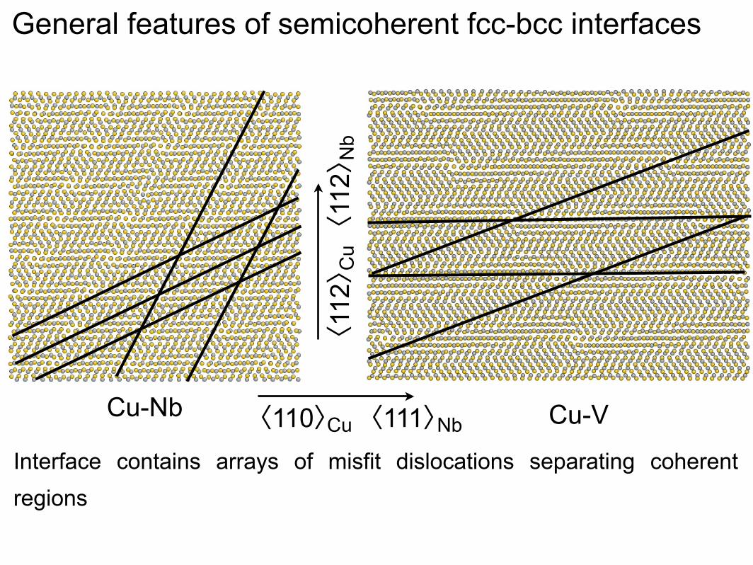
General features of semicoherent fcc-bcc interfaces
Cu-V
〈110〉Cu〈111〉Nb
〈112〉 Cu〈112〉 Nb
An example of a semicoherent interface

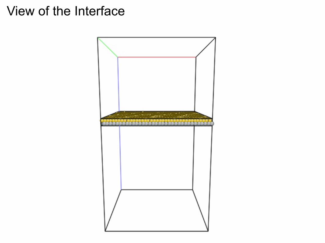
View of the Interface
View of the Interface

View of the Interface

View of the Interface

View of the Interface

View of the Interface

General features of semicoherent fcc-bcc interfaces
Cu-V
〈110〉Cu〈111〉Nb
〈112〉 Cu〈112〉 Nb
An example of a fcc-bcc semicoherent interface
Patterns corresponding to periodic “good” and “bad” regions

General features of semicoherent fcc-bcc interfaces
Cu-V
〈110〉Cu〈111〉Nb
〈112〉 Cu〈112〉 Nb
Interface contains arrays of misfit dislocations separating coherent regions
General features of semicoherent fcc-bcc interfaces
〈110〉Cu〈111〉Nb
〈11
2〉C
u〈
112〉
Nb
Cu-Nb Cu-V
Interface contains arrays of misfit dislocations separating coherent regions

Cu-Nb KS Cu-V KS〈110〉Cu
〈11
2〉C
u1 nm
MDI
• Two sets of misfit dislocations with Burgers vectors
• Misfit dislocation intersections (MDI) where different sets of dislocations meet
General features of semicoherent fcc-bcc interfaces

Outline
• Structure and properties of semicoherent interfaces
• Point defects at semicoherent interfaces
• Migration of point defects and relation to the interface structure
• Implications to ceramic interfaces
• case of MgO grain boundaries

Defects on misfit dislocations are good traps to point defects
0
0
0.2
0.4
0.6
0.8
1
0 0.2 0.4 0.6 0.8 1
0
50
100
150
0
0.2
0.4
0.6
0.8
1
0 0.2 0.4 0.6 0.8 1
0.15
0.2
0.25
0.3
0.35
0.4
0.45
0.5
0
0
0.2
0.4
0.6
0.8
1
0 0.2 0.4 0.6 0.8 1
0
50
100
150
0
0.2
0.4
0.6
0.8
1
0 0.2 0.4 0.6 0.8 1
0.05
0.1
0.15
0.2
0.25
0.3
0.35
0.4
0.45
0.5
0.55
Cu-Nb KS Cu-Fe NW Cu-V KS
1 nm
0
0
0.2
0.4
0.6
0.8
1
0 0.2 0.4 0.6 0.8 1
0
50
100
150
0
0.2
0.4
0.6
0.8
1
0 0.2 0.4 0.6 0.8 1
0.06
0.08
0.1
0.12
0.14
0.16
0.18
0.2
0.22
0.24
0.26
0.28
0
0.2
0.4
0.6
0.8
1
0 0.2 0.4 0.6 0.8 1
0.6
0.8
1
1.2
1.4
0
0.2
0.4
0.6
0.8
1
0 0.2 0.4 0.6 0.8 1
0.6
0.8
1
1.2
1.4
0
0.2
0.4
0.6
0.8
1
0 0.2 0.4 0.6 0.8 1
0.6
0.8
1
1.2
1.4
1 nm 1.4 nm
Form
atio
n en
ergy
(eV
)A
ngle
with
-ve
x ax
is
0
0
0.2
0.4
0.6
0.8
1
0 0.2 0.4 0.6 0.8 1
0
50
100
150
0
0.2
0.4
0.6
0.8
1
0 0.2 0.4 0.6 0.8 1
0.15
0.2
0.25
0.3
0.35
0.4
0.45
0.5
0
0
0.2
0.4
0.6
0.8
1
0 0.2 0.4 0.6 0.8 1
0
50
100
150
0
0.2
0.4
0.6
0.8
1
0 0.2 0.4 0.6 0.8 1
0.05
0.1
0.15
0.2
0.25
0.3
0.35
0.4
0.45
0.5
0.55
Cu-Nb KS Cu-Fe NW Cu-V KS
1 nm
0
0
0.2
0.4
0.6
0.8
1
0 0.2 0.4 0.6 0.8 1
0
50
100
150
0
0.2
0.4
0.6
0.8
1
0 0.2 0.4 0.6 0.8 1
0.06
0.08
0.1
0.12
0.14
0.16
0.18
0.2
0.22
0.24
0.26
0.28
0
0.2
0.4
0.6
0.8
1
0 0.2 0.4 0.6 0.8 1
0.6
0.8
1
1.2
1.4
0
0.2
0.4
0.6
0.8
1
0 0.2 0.4 0.6 0.8 1
0.6
0.8
1
1.2
1.4
0
0.2
0.4
0.6
0.8
1
0 0.2 0.4 0.6 0.8 1
0.6
0.8
1
1.2
1.4
1 nm 1.4 nm
Form
atio
n en
ergy
(eV
)A
ngle
with
-ve
x ax
is
Different fcc-bcc semicoherent interfaces with misfit dislocations
Vacancy formation energies (similar trend for interstitials as well)

Vacancy Interstitial
Structure of isolated point defects in Cu-Nb
• Defect at these interfaces “delocalize”
• knowledge of transport in bulk can not be ported
Outline
• Structure and properties of semicoherent interfaces
• Point defects at semicoherent interfaces
• Migration of point defects and relation to the interface structure
• Implications to ceramic interfaces
• case of MgO grain boundaries

• Migration is along set of dislocation that is predominantly screw
• In the intermediate step, the point defect is delocalized on two MDI
Vacancy
Interstitial
Point defects migrate from one MDI to another in CuNb

b1
!1
Set 2
Set 1
L
a2 a1 Set 1
Set 2
a1
a2
L
Lb1
!1
b1
!1
Set 1
Set 2
3L
• Thermal kink pairs nucleating at adjacent MDI mediate the migration
• Migration barriers 1/3rd that of migration barriers in bulk
KJ1
KJ3´KJ4
Cu
〈112〉
〈110〉Cu
KJ2´
KJ4
KJ3
KJ2KJ1
Cu
〈112〉
〈110〉Cu
a bIVacancy
Step 1
! (reaction coordinate)
t
ca
I
t t
b
" E
(eV
)
0
0.05
0.1
0.15
0.2
0.25
0.3
0.35
0.4
0.45
0 0.1 0.2 0.3 0.4 0.5 0.6 0.7 0.8 0.9 1
t
I
t
b
t
"Ea-b = 0.06 - 0.12 eV"Ea-I = 0.25 - 0.35 eV"Ea-t = 0.35 - 0.45 eV
VacancyInterstitial
Isolated point defects in CuNb migrate from one MDI to another

Isolated point defects in CuNb migrate from one MDI to another

Isolated point defects in CuNb migrate from one MDI to another

b1
!1
Set 2
Set 1
L
a2 a1 Set 1
Set 2
a1
a2
L
Lb1
!1
b1
!1
Set 1
Set 2
3L
KJ1
KJ3´KJ4
Cu
〈112〉
〈110〉Cu
KJ2´
KJ4
KJ3
KJ2KJ1
Cu
〈112〉
〈110〉Cu
a bIVacancy
Step 1
! (reaction coordinate)
t
ca
I
t t
b
" E
(eV
)
0
0.05
0.1
0.15
0.2
0.25
0.3
0.35
0.4
0.45
0 0.1 0.2 0.3 0.4 0.5 0.6 0.7 0.8 0.9 1
t
I
t
b
t
"Ea-b = 0.06 - 0.12 eV"Ea-I = 0.25 - 0.35 eV"Ea-t = 0.35 - 0.45 eV
VacancyInterstitial
Isolated point defects in CuNb migrate from one MDI to another
• Thermal kink pairs nucleating at adjacent MDI mediate the migration
• Migration barriers 1/3rd that of migration barriers in bulk
Set 2
b1
!1
a1
a2
Set 1
L
L
b1!1
Set 1
Set 2
b1
!1
Set 1
Set 2
3L
KJ1
KJ3´KJ4
KJ2´
Cu
〈112〉
〈110〉Cu
cb IVacancy
Step 2
! (reaction coordinate)
t
ca
I
t t
b
" E
(eV
)
0
0.05
0.1
0.15
0.2
0.25
0.3
0.35
0.4
0.45
0 0.1 0.2 0.3 0.4 0.5 0.6 0.7 0.8 0.9 1
t
I
t
b
t
"Ea-b = 0.06 - 0.12 eV"Ea-I = 0.25 - 0.35 eV"Ea-t = 0.35 - 0.45 eV
VacancyInterstitial
Thermal kink pairs aid the migration process
• Thermal kink pairs nucleating at adjacent MDI mediate the migration
• Migration barriers 1/3rd that of migration barriers in bulk

The width of the nucleating thermal kink pairs determines the barrier
ΔEact = 0.35 - 0.45 eV ΔEact = 0.60 - 0.67 eV
(d) (e) (f)
Vacancy
(a) (b) (c)
Interstitial
1nm
Thermal kink pairs aid the migration process

Multiple migration paths and detours
Migration paths (CI-NEB)
• Not all intermediate states need to be visited in every migration
• The underlying physical phenomenon, however, remains unchanged
! (reaction coordinate)
t
ca
I
t t
b "
E (
eV
)
0
0.05
0.1
0.15
0.2
0.25
0.3
0.35
0.4
0.45
0 0.1 0.2 0.3 0.4 0.5 0.6 0.7 0.8 0.9 1
t
I
t
b
t
"Ea-b = 0.06 - 0.12 eV"Ea-I = 0.25 - 0.35 eV"Ea-t = 0.35 - 0.45 eV
VacancyInterstitial

Entire migration path can be predicted
Key inputs to the dislocation model
• Interface misfit dislocation distribution
• Structure of the accommodated point defects
Analysis of the interface structure may help predict quantitatively
point-defect behavior at other semicoherent interfaces
Δ E
(eV
)
s s
0
0.05
0.1
0.15
0.2
0.25
0.3
0.35
0.4
0.45
0.5
0.55
0 0.1 0.2 0.3 0.4 0.5 0.6 0.7 0.8 0.9 1
I
a 0
0.05
0.1
0.15
0.2
0.25
0.3
0.35
0.4
0.45
0.5
0 0.1 0.2 0.3 0.4 0.5 0.6 0.7 0.8 0.9 1
b
IDislocation model
Atomistics
K. Kolluri and M. J. Demkowicz, Phys Rev B, 82, 193404 (2010)
KJ1
KJ3´KJ4
Cu
〈112〉
〈110〉Cu
KJ2´
KJ4
KJ3
KJ2KJ1

Point defect migration rates from simulations
FORMATION, MIGRATION, AND CLUSTERING OF . . . PHYSICAL REVIEW B 85, 205416 (2012)
FIG. 15. (Color online) (a) Total energy change (filled squares),kink-jog core energy (filled triangles), and the energy from the dislo-cation model (continuous curve) for the direct migration mechanism.Filled circles show the kink-jog core volume. The arrow on the leftshows the range of formation energies computed for a aCu
4 !112" jogon a screw dislocation in fcc Cu and the arrow on the right shows thecorresponding formation volumes. (b) Plan view of the interface Cu(gold) and Nb (gray) atoms with a point defect in extended state B.Arrows mark the location of kink-jogs, the numbers are values of S,and red lines mark the nominal locations of set 2 misfit dislocationcores.
The above discrepancy arises because the core energy of thejog, which is assumed constant for all states in our dislocationmodel [and therefore does not appear in Eq. (1)], actually variesalong the direct migration path. To estimate the core energyof the kink-jog, we summed differences in atomic energiesbetween the core atoms and corresponding atoms in a defect-free interface. The kink-jog core is taken to consist of 19 atoms:the 5-atom ring in the Cu terminal plane and the 7 neighboringCu and Nb atoms from each of the two planes adjacent to the Cuterminal plane. Core volumes were computed in an analogousway. The core energies of the migrating jog are plotted asfilled triangles in Fig. 15(a) and are in good semiquantitativeagreement with the overall energy changes occurring alongthe direct migration path. Core volumes are plotted as filledcircles.
Figure 15(b) shows the Cu and Nb interface planes witha point defect in the extended state B. Arrows mark thelocations of the two kink-jogs and red lines mark the nominallocations of set 2 misfit dislocation cores. The numbers are
values of the displacement parameter S. At all values of Sexcept S # {3,4}, the kink-jog resides in the vicinity of a set2 misfit dislocation, which affects its structure. The atomicconfigurations of the kink-jog at S # {3,4} were compared tothat of a constricted l = aCu
4 !112" jog on a screw dislocationin fcc Cu.61,62 Depending on the choice of reference energiesand volumes, the core energy and volume of the l = aCu
4 !112"jog were found to be $0.8%1.1 eV and $0.4!o%0.6!o,respectively, where !o = 13.339 A3 is the atomic volume offcc Cu. These values compare very well with those obtainedfor the jog at S # {3,4}, which are also the states where thekink-jog core energy is largest.
Thus, the true energy barrier for the direct migrationmechanism is roughly equal to the difference in the formationenergies of the jog at the MDI and that of an isolated jog on ascrew dislocation. The dislocation model may be modified toaccount for such a behavior by allowing the core radius " tochange with the distance between the jogs (S). Although irrel-evant in the Cu-Nb interface, the direct migration mechanismmay occur in other interfaces where the activation energy forthermal-kink-pair nucleation is comparable to the differencein kink-jog core energies described above. Furthermore, weexpect that the direct migration mechanism, when active,would be highly pressure sensitive on account of its highactivation volume.
D. Temperature dependence of point defect migration
As described in Sec. III C, delocalized interface pointdefects jump between MDIs through multiple steps. KineticMonte Carlo (kMC) simulations63 may be used to determinethe temperature dependence of the effective migration ratedue to these numerous transitions. Since the vacancy andinterstitial migration is along set 1 misfit dislocations, weconsider migration only in one dimension. The transitions wetake into account along with their activation energies are listedin Table I. In each transition listed in Table I, the start and endstates are connected through just one path, but there may bemore than one end state accessible for a given starting state.For example, a defect at its initial state A has two I states,
TABLE I. Transitions occurring during migration of individualpoint defects that were considered in kMC simulations, theircorresponding activation energy barriers, and number of distinct endstates for a given start state.
Transition Activation energy Number oftype (eV) distinct end states
A & I 0.40 2A & B 0.40 2I (near A) & B 0.15 1I (near A) & A 0.15 1B & A 0.35 1B & I 0.35 2B & I ' 0.20 1B & C 0.35 1I (near C) & C 0.15 1I (near C) & B 0.15 1I ' & B 0.15 1
205416-9
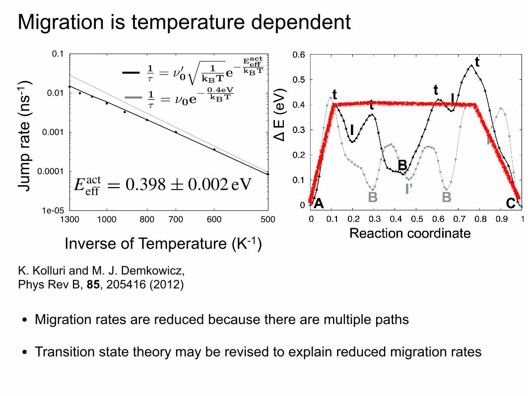
• Hypothesis:
• transition state theory is valid and
• Rate-limiting step will determine the migration rate ≥ 0.4 eV
• Validation:
• kinetic Monte Carlo (since the migration path is not trivial)
• Statistics from molecular dynamics

Jum
p ra
te (n
s-1) 1
� = �0e� 0.4eV
kBT
1e-05
0.0001
0.001
0.01
0.1
1300 1000 800 700 600 500
Inverse of Temperature (K-1)
• Migration rates are reduced because there are multiple paths
• Transition state theory may be revised to explain reduced migration rates
Migration is temperature dependent
K. Kolluri and M. J. Demkowicz,Phys Rev B, 85, 205416 (2012)

Jum
p ra
te (n
s-1)
1e-05
0.0001
0.001
0.01
0.1
1300 1000 800 700 600 500
Inverse of Temperature (K-1)
Migration is temperature dependent
1� = �0e
� 0.4eVkBT
• Migration rates are reduced because there are multiple paths
• Transition state theory may be revised to explain reduced migration rates
K. Kolluri and M. J. Demkowicz,Phys Rev B, 85, 205416 (2012)
Jum
p ra
te (n
s-1)
1� = �⇥0
�1
kBTe�Eacte�
kBT
1� = �0e
� 0.4eVkBT
1e-05
0.0001
0.001
0.01
0.1
1300 1000 800 700 600 500
Inverse of Temperature (K-1)
Migration is temperature dependent
FORMATION, MIGRATION, AND CLUSTERING OF . . . PHYSICAL REVIEW B 85, 205416 (2012)
migration process with their multiple minima may be thoughtof as a single “flat” degree of freedom at the saddle point.65
Taking initial and final states corresponding to a defectresiding at neighboring MDIs, we attempt to represent all ofthe intermediate states with a single “effective” saddle pointof this kind. To account for the multiple states that comprisethe effective saddle point, we consider the saddle point tobe a hypersurface with one translational mode. Therefore,the saddle point has N ! 2 vibrational degrees of freedominstead of N ! 1 degrees of freedom as in the case of migrationinvolving a single jump through a unique saddle point. Hence,Eqs. (5) and (6) become
! =!
kBT
2"
A0"N!2
j=11# "j
#kBT2"
"Nj=1
1#j
#kBT2"
e! E(S)
kB T
e! E(A)
kB T
, (7)
! =
$2"
kBT
A0"N!2
j=11# "j"N
j=11#j
e! E(S)!E(A)
kB T = # "0
1#kBT
e! Eact
kB T , (8)
where A0 is a constant contributed by the translational mode65
to the configurational partition function. The attempt fre-quency predicted by this expression is temperature dependent.
The expression in Eq. (8) is identical to those obtainedfor models of an overdamped elastic spring on a nonlinearpotential surface. Such a spring also has a translational modeand has been used as a model for nucleation and motion of kinkpairs on overdamped solitons in spatially one-dimensionalsystems65–69 and for nucleation of kink pairs on dislocationsin two-dimensional Frankel-Kontorova models.70 Our kMCresults fit very well to Eq. (8) with an effective activationbarrier Eact
eff = 0.398 ± 0.002 eV, as illustrated by the blackline in Fig. 16(a).
The numerical value of the # "0 may be determined directly
from MD simulations by counting the number of times a defectjumps from one MDI to another in a fixed time interval.We assumed that point defect migration follows a Poissonprocess71 in which the probability that exactly s events occurin a time interval t is given by
p(t/$,s) = (t/$ )se!t/$
s!. (9)
Here, $ = 1!
is the average waiting time for a defectto migrate to an adjacent MDI. We performed N0 = 64independent MD runs of a vacancy at an MDI in the Cu-Nb
interface. These runs were repeated at three different temper-atures: T $ {600,700,800} K. The duration of each run was8.11 ns (ttot). In each run, migration events were identified bydirect inspection of atomic configurations recorded at intervalsof 40.5 ps. From the investigation described in Sec. III C1,we know that the typical duration of a complete migrationevent at T = 800 K is 32.5 ps. Thus, the selected timeinterval between consecutive recordings minimizes the totalnumber of configurations that must be saved and analyzedwhile ensuring that no more than one migration event occursbetween recordings. While no migration events were observedin some runs, as many as three distinct ones were observedin others. For a given temperature, we identify the probabilityp(ttot/$,s) = n(s)
N0that the point defect migrated to an adjacent
MDI exactly s times, where n(s) is the number of runs in whichexactly s migration events occurred and plotted in Fig. 17 ashistograms. We use these probabilities to determine $ from aleast-squares fit in s to
ln[(s!)p(t/$,s)] = s ln(t/$ ) ! t/$. (10)
Good fits are obtained for all three temperatures, confirmingour assumption that point defect migration follows a Poissonprocess (Fig. 17). The jump rates for each temperature,obtained by fitting, are plotted in Fig. 16(b) as filled graycircles with uncertainties corresponding to the error in theleast-squares fit. The gray line is the least-squares fit of Eq. (8)to the rates obtained from MD. The activation energy obtainedfrom our kMC model (Eact
eff = 0.398 ± 0.002 eV) is well withinthe uncertainty of the activation energy found by fitting the MDdata, namely, Eact
eff = 0.374 ± 0.045 eV.The effective attempt frequency for defect migration ob-
tained by fitting the MD data is # "0 = 6.658 % 109 ± 2.7 %
106 s!1. This value is several orders of magnitude lower thantypical attempt frequencies for point defect migration in fccCu, namely, 1012!1014 s!1.72–74 A mechanistic interpretationfor such a low migration attempt frequency is not immediatelyforthcoming. One possible explanation is that it arises fromthe large number of atoms participating in the migrationprocess. The attempt frequency for migration of compact pointdefects might be expected to be on the order of the Einsteinfrequency because it involves the motion of only one atom.However, the migration mechanism discussed here involvescollective motion of many atoms. Their collective oscillationin a vibrational mode that leads up to the saddle point fordefect migration may have a considerably lower frequency
FIG. 17. Comparison between the MD data (histograms) to the fits obtained by assuming that point defect migration follows a Poissonprocess (continuous curves and data points).
205416-11
• Migration rates are reduced because there are multiple paths
• Transition state theory may be revised to explain reduced migration rates
K. Kolluri and M. J. Demkowicz,Phys Rev B, 85, 205416 (2012)

MDkMC
0.001
0.01
0.1
1
1300 1000 800 700 600 500
Jum
p ra
te (n
s-1)
Inverse of Temperature (K-1)
Migration is temperature dependent
• Modified rate expression is fit to MD statistics to obtain attempt frequency
• Attempt frequency is much lower than is normally observed for point defects
model(Eact
eff
= 0.398±0.002 eV) is well within the uncertainty of the activation energy found
by fitting the MD data, namely E
act
eff
= 0.374± 0.045 eV.
⌫
00 = 6.658⇥ 109 ± 2.7⇥ 106s�1 The effective attempt frequency for defect migration ob-
tained by fitting the MD data is ⌫ 00 = 6.658⇥ 109 ± 2.7⇥ 106s�1.This value is several orders
of magnitude lower than typical attempt frequencies for point defect migration in fcc Cu,
namely 1012�1014 s�1 69–71. A mechanistic interpretation for such a low migration attempt
frequency is not immediately forthcoming. One possible explanation is that it arises from
the large number of atoms participating in the migration process. The attempt frequency
for migration of compact point defects might be expected to be on the order of the Einstein
frequency because it involves the motion of only one atom. However, the migration mech-
anism discussed here involves collective motion of many atoms. Their collective oscillation
in a vibrational mode that leads up to the saddle point for defect migration may have a
considerably lower frequency than an Einstein oscillator. This interpretation, however, is
at odds with other collective processes, such as the spontaneous transformation of small
voids to stacking fault tetrahedra, whose effective attempt frequency was several orders of
magnitude higher than the Einstein frequency72.
Delocalized point defect migration from one MDI to another may also involve passage
through several intermediate metastable states that do not assist migration: the I0 states
described in section III C 1. Therefore, the defect is likely to spend more time between
the initial and final states than it would had there been only one saddle point, lowering
the effective attempt frequency. If this were to completely account for the lowering of the
attempt frequency, however, then nucleation of I0 states would have to occur several orders
of magnitude more frequently than the completion of a migration step, which is not what we
observe. Finally, conventional transition state theory overestimates attempt frequencies by
assuming that every time a point defect crosses the saddle point, it reaches the final state.
In reality, however, a saddle point may be recrossed several times before reaching the final
state73, reducing the value of the pre-factor as derived by transition state theory61. Further
work is needed to determine which, if any, of these explanations is the correct one.
28
model(Eact
eff
= 0.398±0.002 eV) is well within the uncertainty of the activation energy found
by fitting the MD data, namely E
act
eff
= 0.374± 0.045 eV.
E
act
eff
= 0.374± 0.045 eV ⌫
00 = 6.658⇥ 109 ± 2.7⇥ 106s�1 The effective attempt frequency
for defect migration obtained by fitting the MD data is ⌫ 00 = 6.658⇥ 109± 2.7⇥ 106s�1.This
value is several orders of magnitude lower than typical attempt frequencies for point defect
migration in fcc Cu, namely 1012�1014 s�1 69–71. A mechanistic interpretation for such a
low migration attempt frequency is not immediately forthcoming. One possible explanation
is that it arises from the large number of atoms participating in the migration process. The
attempt frequency for migration of compact point defects might be expected to be on the or-
der of the Einstein frequency because it involves the motion of only one atom. However, the
migration mechanism discussed here involves collective motion of many atoms. Their collec-
tive oscillation in a vibrational mode that leads up to the saddle point for defect migration
may have a considerably lower frequency than an Einstein oscillator. This interpretation,
however, is at odds with other collective processes, such as the spontaneous transformation
of small voids to stacking fault tetrahedra, whose effective attempt frequency was several
orders of magnitude higher than the Einstein frequency72.
Delocalized point defect migration from one MDI to another may also involve passage
through several intermediate metastable states that do not assist migration: the I0 states
described in section III C 1. Therefore, the defect is likely to spend more time between
the initial and final states than it would had there been only one saddle point, lowering
the effective attempt frequency. If this were to completely account for the lowering of the
attempt frequency, however, then nucleation of I0 states would have to occur several orders
of magnitude more frequently than the completion of a migration step, which is not what we
observe. Finally, conventional transition state theory overestimates attempt frequencies by
assuming that every time a point defect crosses the saddle point, it reaches the final state.
In reality, however, a saddle point may be recrossed several times before reaching the final
state73, reducing the value of the pre-factor as derived by transition state theory61. Further
work is needed to determine which, if any, of these explanations is the correct one.
28
K. Kolluri and M. J. Demkowicz, Phys Rev B, 85, 205416 (2012)

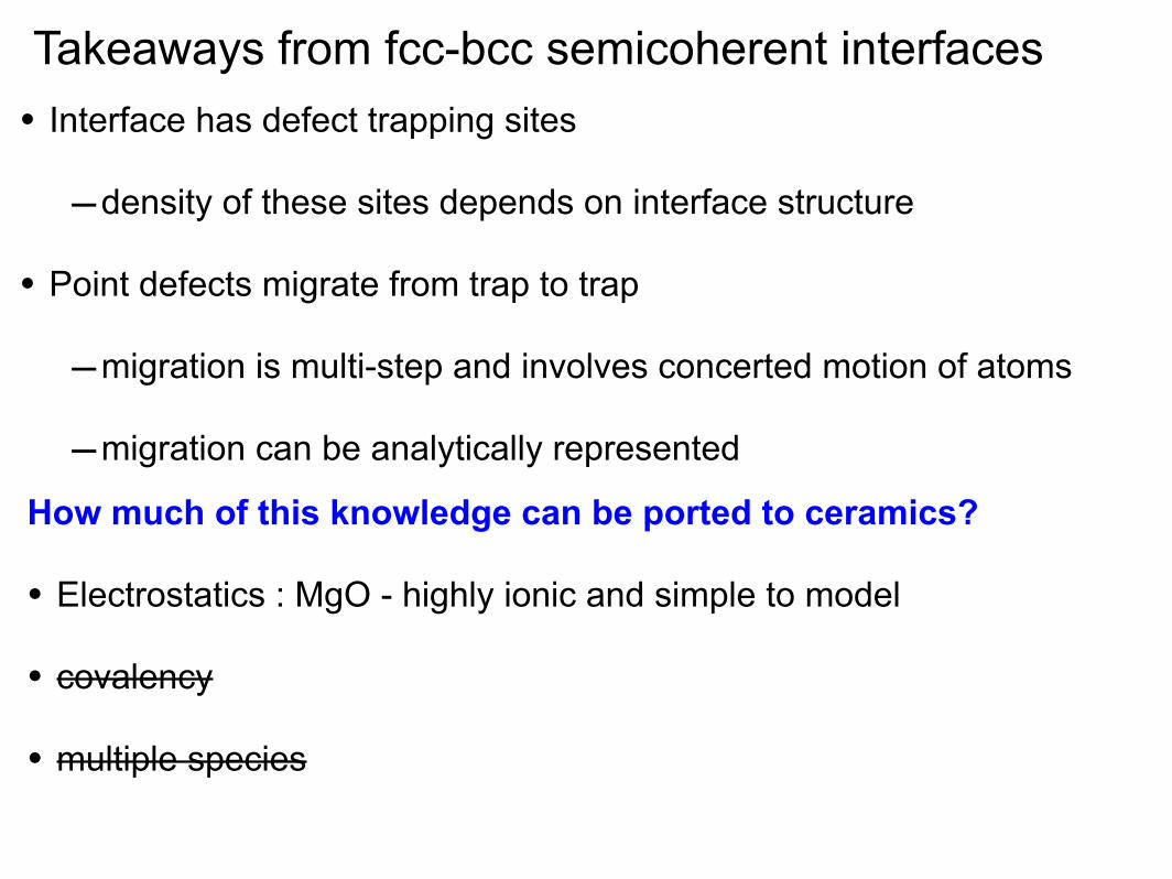
Takeaways from fcc-bcc semicoherent interfaces• Interface has defect trapping sites
–density of these sites depends on interface structure
• Point defects migrate from trap to trap
–migration is multi-step and involves concerted motion of atoms
–migration can be analytically represented
How much of this knowledge can be ported to ceramics?
• Electrostatics
• covalency
• multiple species
Takeaways from fcc-bcc semicoherent interfaces• Interface has defect trapping sites
–density of these sites depends on interface structure
• Point defects migrate from trap to trap
–migration is multi-step and involves concerted motion of atoms
–migration can be analytically represented
How much of this knowledge can be ported to ceramics?
• Electrostatics : MgO - highly ionic and simple to model
• covalency
• multiple species
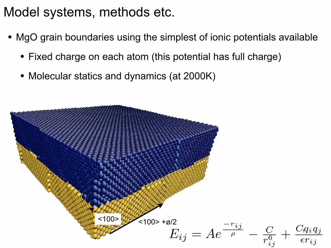
Model systems, methods etc.
1 nm• MgO grain boundaries using the simplest of ionic potentials available
• Fixed charge on each atom (this potential has full charge)
• Molecular statics and dynamics (at 2000K)
<100> <100> +ø/2
Eij = Ae�rij
⇢ � Cr6ij
+ Cqiqj✏rij1

1 nm• Grain boundaries (3.5º to 10º)
3.476º, 4.969º, 7.5º, 10.393º
d = 34Å
Model systems

1 nm
d = 15Å
Model systems
• Grain boundaries (3.5º to 10º)
3.476º, 4.969º, 7.5º, 10.393º

Ground-state structure of (some) grain boundaries
Electrostatics: 2 MgO units less at an MDI (O-lattice points)
-2
-1.5
-1
-0.5
0
0.5
0 0.5 1 1.5 2

Typical interface (one with misfit dislocations)
7.5º twist boundary

Vacancy delocalizes on the misfit dislocation
• Farther, the “halves” of the vacancy, the lower is the energy
• But, not farthest!
Electrostatics

• Differences with metal-metal interfaces
• Vacancies delocalize at misfit dislocations
• MDIs hollow and can not reconstruct
0
0.05
0.1
0.15
0.2
0.25
0.3
0.35
0.4
0.45
0 1 2 3 4 5 6 7 8
Ef (
eV)
8 7 6 5 4 3 2 1 0
Vacancy delocalizes on the misfit dislocation

Summary of where O vacancy traps
At MDI
Ef (
eV)
Adjacent planes
-0.3
-0.25
-0.2
-0.15
-0.1
-0.05
0
0.05
0.1
0.15
0 1 2 3 4 5 6 7 81234567 localizedat MD

123456
At MDI
localizedat MD
Ef (
eV)
Adjacent planes
-0.35-0.3
-0.25-0.2
-0.15-0.1
-0.05 0
0.05 0.1
0.15 0.2
0 1 2 3 4 5 6 7
Summary of where Mg vacancy traps
7

Interaction energies Wint
= Welastic
+Welectrostatic
nL
a 11W
elastic
⇡ µb2a2
8⇡(1� ⌫)
1
nL
Welectrostatic
⇡ q1q24⇡✏0
1
nL
b =a0p2
a =a02
µ = 155 GPa
⌫ = 0.18
L = b
q1, q2 = 1e
✏0 = 8.85e�12 Ohm�1m�1
a0 = 4.212A
Welectrostatic
=q1q24⇡✏0✏
1
nL
✏this model
= 7.92
Welectrostatic
=0.606
n
Welastic = �0.63(0.68)
neV
eV n - number of nearest neighbors
132-141 GPa
0.32
• Elastic energies are perhaps an overestimate!

Oxygen vacancy transport in GB with misfit dislocations
Oxygen vacancy at 7.5º GB

Direct observation
t0 t0 +4 ps t0 +8 ps
0.2 - 0.3 eV
0.3 eV
NOT TO SCALE
• Migration barriers 1/10th that of migration barriers in bulk

SummaryMetals:
• Interface has defect trapping sites
–density of these sites depends on interface structure
• Point defects migrate from trap to trap
–migration is multi-step and involves concerted motion of atoms
–migration can be analytically represented
Ceramics:
• Defects trapped at and migrate from one misfit dislocation to another
• Electrostatics in the model ceramics play greater role
• Defects migrate faster and anisotropic
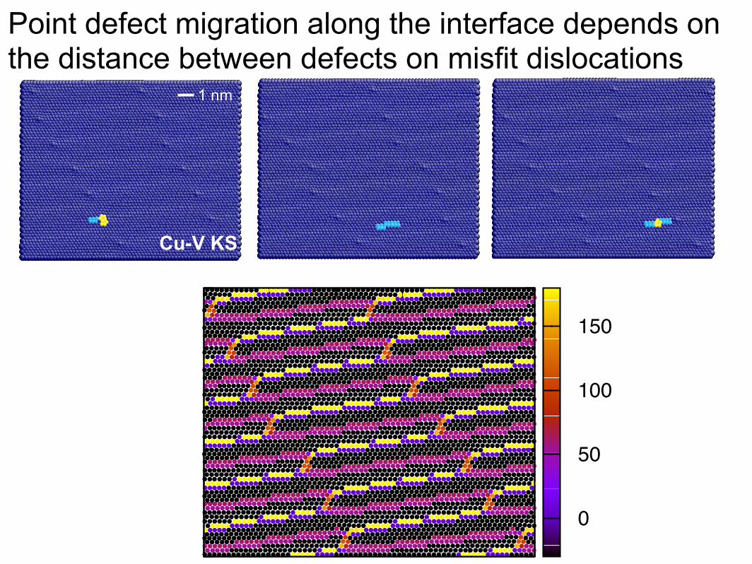
Point defect migration along the interface depends on the distance between defects on misfit dislocations0
0
0.2
0.4
0.6
0.8
1
0 0.2 0.4 0.6 0.8 1
0
50
100
150
0
0.2
0.4
0.6
0.8
1
0 0.2 0.4 0.6 0.8 1
0.05
0.1
0.15
0.2
0.25
0.3
0.35
0.4
0.45
0.5
0.55
1 nm
Cu-V KS

2.9
2.95
3
3.05
3.1
3.15
3.2
3.25
3.3
0.48 0.49 0.5 0.51 0.52 0.53 0.54 0.55 0.56
• Similarities with metal-metal interfaces
• dislocations and MDIs are preferred sites for point defects
Ef (
eV)
z axis
Oxygen vacancy at grain boundaries at 5º twist

2.9
2.95
3
3.05
3.1
3.15
3.2
3.25
3.3
0.48 0.49 0.5 0.51 0.52 0.53 0.54 0.55 0.56
• Differences with metal-metal interfaces
• point defects reside in adjacent planes at MDIs
Ef (
eV)
z axis
Oxygen vacancy at grain boundaries at 5º twist