aes in fpga.pdf
169
Technical Report Number 763 Computer Laboratory UCAM-CL-TR-763 ISSN 1476-2986 Security for volatile FPGAs Saar Drimer November 2009 15 JJ Thomson Avenue Cambridge CB3 0FD United Kingdom phone +44 1223 763500 http://www.cl.cam.ac.uk/
-
Upload
chandan-choudhury -
Category
Documents
-
view
72 -
download
1
description
aes specification for fpga
Transcript of aes in fpga.pdf
Technical ReportNumber 763
Computer Laboratory
UCAM-CL-TR-763ISSN 1476-2986
Security for volatile FPGAs
Saar Drimer
November 2009
15 JJ Thomson AvenueCambridge CB3 0FDUnited Kingdomphone +44 1223 763500
http://www.cl.cam.ac.uk/

c© 2009 Saar Drimer
This technical report is based on a dissertation submittedAugust 2009 by the author for the degree of Doctor ofPhilosophy to the University of Cambridge, Darwin College.
Technical reports published by the University of CambridgeComputer Laboratory are freely available via the Internet:
http://www.cl.cam.ac.uk/techreports/
ISSN 1476-2986

Security for volatile FPGAs
Saar Drimer
Summary
With reconfigurable devices fast becoming complete systems in their own right,
interest in their security properties has increased. While research on “FPGA sec-
urity” has been active since the early 2000s, few have treated the field as a whole,
or framed its challenges in the context of the unique FPGA usage model and ap-
plication space. This dissertation sets out to examine the role of FPGAs within a
security system and how solutions to security challenges can be provided. I offer the
following contributions.
I motivate authenticating configurations as an additional capability to FPGA
configuration logic, and then describe a flexible security protocol for remote recon-
figuration of FPGA-based systems over insecure networks. Non-volatile memory
devices are used for persistent storage when required, and complement the lack of
features in some FPGAs with tamper proofing in order to maintain specified secur-
ity properties. A unique advantage of the protocol is that it can be implemented
on some existing FPGAs (i.e., it does not require FPGA vendors to add function-
ality to their devices). Also proposed is a solution to the “IP distribution problem”
where designs from multiple sources are integrated into a single bitstream, yet must
maintain their confidentiality.
I discuss the difficulty of reproducing and comparing FPGA implementation re-
sults reported in the academic literature. Concentrating on cryptographic implemen-
tations, problems are demonstrated through designing three architecture-optimized
variants of the AES block cipher and analyzing the results to show that single fig-
ures of merit, namely “throughput” or “throughput per slice”, are often meaningless
without the context of an application. To set a precedent for reproducibility in our
field, the HDL source code, simulation testbenches and compilation instructions are
made publicly available for scrutiny and reuse.
Finally, I examine payment systems as ubiquitous embedded devices, and evalu-
ate their security vulnerabilities as they interact in a multi-chip environment. Using
FPGAs as an adversarial tool, a man-in-the-middle attack against these devices is
demonstrated. An FPGA-based defense is also demonstrated: the first secure wired
“distance bounding” protocol implementation. This is then put in the context of
securing reconfigurable systems.
Acknowledgments
I dedicate this dissertation to my parents, Mika and Gideon, for their unconditional
love and support throughout my life, and to my kind siblings Hadar and Oz, and
their families. They have all seen less of me than they deserved in the past twelve
years as I was pursuing my goals.
Markus Kuhn, my supervisor, has been an influential part of my academic de-
velopment, and I thank him for his guidance, especially on how to produce solid
research. I thank Ross Anderson for valuable lessons on security in the real world
through our collaborations and conversations. I enjoyed collaborating with Steven
Murdoch on our banking security projects, and I also thank current and past mem-
bers of the Security Group – in particular, Mike Bond, Richard Clayton, Robert
Watson, Gerhard Hancke, Shishir Nagaraja, Frank Stajano, Dan Cvrcek, and Tyler
Moore – for listening, teaching, and reading my drafts, but also for our stimulating
conversations about security, life, and everything else. I’m also grateful for com-
ments from my examiners, Ingrid Verbauwhede and Simon Moore.
I’m fortunate to have been the recipient of a generous research grant from Xilinx.
On that interview day as a new college grad I was privileged to have met my mentor
and friend Austin Lesea; I thank him for being exactly the person he is. At Xilinx,
Steve Trimberger, Jason Moore, Jesse Jenkins and Neil Jacobson were always there
to provide technical assistance, but much more importantly, they shared their life ex-
periences with me. Christof Paar and Tim Guneysu hosted me at Ruhr-Universitat
Bochum for three months. I thank them and the rest of the CoSY group for a
productive time and for their hospitality. Additional financial support was kindly
provided by the Computer Laboratory and Darwin College.
Sabine, my first Cambridge friend, kept me sane at the onset by our frequent
bike excursions around Cambridge. My friendship with Shlomy meant a lot to me,
as I could always rely on him for help and good company. Other friends gave me
“a life” outside the “lab”: Dan T, Alban, Margaret, Matt, Davide, Philip, Bogdan,
Niki, Andreas, and Satnam. To my friends from the rest of the world – Amir, Ron,
Udi, Assaf, Nir D, Nir S, Phil, Kristin, Max – you are not forgotten, even though
I’ve been distant. In particular, Sina and Dirk always believed in me more than I
believed in myself; I thank them for their consistent encouragement. A fortuitous
conference seating arrangement introduced me to Owen, who simply wants a lot of
“freedom”; I thank him for keeping the dream alive during the dark times.
Lastly, the love and encouragement from Caroline got me through all of this;
thank you, my dear.
Saar Drimer, Cambridge, UK, August 2009
Contents
1 Introduction 111.1 Motivation and contribution . . . . . . . . . . . . . . . . . . . . . . . 121.2 Reading this dissertation . . . . . . . . . . . . . . . . . . . . . . . . . 14
2 FPGA security foundations 172.1 FPGA usage model . . . . . . . . . . . . . . . . . . . . . . . . . . . . 18
2.1.1 Principals . . . . . . . . . . . . . . . . . . . . . . . . . . . . . 182.1.2 Design and manufacturing flow . . . . . . . . . . . . . . . . . 222.1.3 Defense categories . . . . . . . . . . . . . . . . . . . . . . . . . 242.1.4 Trust and trustworthiness . . . . . . . . . . . . . . . . . . . . 252.1.5 Distribution security . . . . . . . . . . . . . . . . . . . . . . . 26
2.2 Usage model attacks . . . . . . . . . . . . . . . . . . . . . . . . . . . 272.2.1 Bitstream reverse engineering . . . . . . . . . . . . . . . . . . 292.2.2 Counterfeits . . . . . . . . . . . . . . . . . . . . . . . . . . . . 312.2.3 Readback . . . . . . . . . . . . . . . . . . . . . . . . . . . . . 332.2.4 Side-channels . . . . . . . . . . . . . . . . . . . . . . . . . . . 342.2.5 Invasive and semi-invasive attacks . . . . . . . . . . . . . . . . 402.2.6 Others . . . . . . . . . . . . . . . . . . . . . . . . . . . . . . . 42
2.3 Defenses . . . . . . . . . . . . . . . . . . . . . . . . . . . . . . . . . . 442.3.1 Configuration confidentiality . . . . . . . . . . . . . . . . . . . 442.3.2 Configuration authenticity . . . . . . . . . . . . . . . . . . . . 462.3.3 Design theft deterrents . . . . . . . . . . . . . . . . . . . . . . 492.3.4 Watermarking and fingerprinting . . . . . . . . . . . . . . . . 512.3.5 Physical unclonable functions . . . . . . . . . . . . . . . . . . 532.3.6 Evolvable hardware . . . . . . . . . . . . . . . . . . . . . . . . 562.3.7 Isolation . . . . . . . . . . . . . . . . . . . . . . . . . . . . . . 57
2.4 Conclusion . . . . . . . . . . . . . . . . . . . . . . . . . . . . . . . . . 58
3 Secure remote reconfiguration 593.1 Update logic . . . . . . . . . . . . . . . . . . . . . . . . . . . . . . . . 60
3.1.1 Assumptions . . . . . . . . . . . . . . . . . . . . . . . . . . . . 613.1.2 Protocol . . . . . . . . . . . . . . . . . . . . . . . . . . . . . . 623.1.3 Recovery from errors . . . . . . . . . . . . . . . . . . . . . . . 66
3.2 Update server routines . . . . . . . . . . . . . . . . . . . . . . . . . . 663.2.1 Offline operation . . . . . . . . . . . . . . . . . . . . . . . . . 69
3.3 Authenticity and confidentiality . . . . . . . . . . . . . . . . . . . . . 703.4 Multiple NVM slots . . . . . . . . . . . . . . . . . . . . . . . . . . . . 71

3.5 Analysis . . . . . . . . . . . . . . . . . . . . . . . . . . . . . . . . . . 743.6 Implementation considerations . . . . . . . . . . . . . . . . . . . . . . 76
3.6.1 Parameter sizes . . . . . . . . . . . . . . . . . . . . . . . . . . 763.7 Related work . . . . . . . . . . . . . . . . . . . . . . . . . . . . . . . 773.8 Conclusions . . . . . . . . . . . . . . . . . . . . . . . . . . . . . . . . 78
4 AES in spare logic 814.1 Introduction . . . . . . . . . . . . . . . . . . . . . . . . . . . . . . . . 814.2 Prior work . . . . . . . . . . . . . . . . . . . . . . . . . . . . . . . . . 824.3 Implementation . . . . . . . . . . . . . . . . . . . . . . . . . . . . . . 84
4.3.1 AES32 module . . . . . . . . . . . . . . . . . . . . . . . . . . 844.3.2 AES128 and AES128U modules . . . . . . . . . . . . . . . . . 884.3.3 Decryption . . . . . . . . . . . . . . . . . . . . . . . . . . . . 904.3.4 Key expansion . . . . . . . . . . . . . . . . . . . . . . . . . . . 91
4.4 Results . . . . . . . . . . . . . . . . . . . . . . . . . . . . . . . . . . . 914.5 Extensions . . . . . . . . . . . . . . . . . . . . . . . . . . . . . . . . . 94
4.5.1 Message authentication: CMAC . . . . . . . . . . . . . . . . . 944.5.2 CTR and CCM modes . . . . . . . . . . . . . . . . . . . . . . 964.5.3 Replacing DSPs with CLBs . . . . . . . . . . . . . . . . . . . 97
4.6 Conclusions . . . . . . . . . . . . . . . . . . . . . . . . . . . . . . . . 98
5 The meaning and reproducibility of FPGA results 995.1 Demonstration experiments . . . . . . . . . . . . . . . . . . . . . . . 100
5.1.1 Application context . . . . . . . . . . . . . . . . . . . . . . . . 1005.2 Discussion . . . . . . . . . . . . . . . . . . . . . . . . . . . . . . . . . 105
5.2.1 Source code . . . . . . . . . . . . . . . . . . . . . . . . . . . . 1055.2.2 Optimization goals . . . . . . . . . . . . . . . . . . . . . . . . 1085.2.3 Throughput per slice/area . . . . . . . . . . . . . . . . . . . . 1095.2.4 Other hazards . . . . . . . . . . . . . . . . . . . . . . . . . . . 110
5.3 Possible objections . . . . . . . . . . . . . . . . . . . . . . . . . . . . 1115.4 Related work . . . . . . . . . . . . . . . . . . . . . . . . . . . . . . . 1125.5 Conclusions . . . . . . . . . . . . . . . . . . . . . . . . . . . . . . . . 112
6 Distance bounding for wired applications 1156.1 Background . . . . . . . . . . . . . . . . . . . . . . . . . . . . . . . . 1156.2 Relay attack . . . . . . . . . . . . . . . . . . . . . . . . . . . . . . . . 116
6.2.1 Implementation . . . . . . . . . . . . . . . . . . . . . . . . . . 1176.2.2 Procedure and timing . . . . . . . . . . . . . . . . . . . . . . . 1196.2.3 Results . . . . . . . . . . . . . . . . . . . . . . . . . . . . . . . 1206.2.4 Further applications and feasibility . . . . . . . . . . . . . . . 121
6.3 Defenses . . . . . . . . . . . . . . . . . . . . . . . . . . . . . . . . . . 1226.3.1 Non-solutions . . . . . . . . . . . . . . . . . . . . . . . . . . . 1226.3.2 Procedural improvements . . . . . . . . . . . . . . . . . . . . 1246.3.3 Hardware alterations . . . . . . . . . . . . . . . . . . . . . . . 125
6.4 Distance bounding . . . . . . . . . . . . . . . . . . . . . . . . . . . . 1256.4.1 Protocol . . . . . . . . . . . . . . . . . . . . . . . . . . . . . . 1266.4.2 Implementation . . . . . . . . . . . . . . . . . . . . . . . . . . 1286.4.3 Circuit elements and signals . . . . . . . . . . . . . . . . . . . 128
6.4.4 Possible attacks on distance bounding . . . . . . . . . . . . . . 1326.4.5 Results . . . . . . . . . . . . . . . . . . . . . . . . . . . . . . . 1336.4.6 Costs . . . . . . . . . . . . . . . . . . . . . . . . . . . . . . . . 135
6.5 Distance bounding in FPGA applications . . . . . . . . . . . . . . . . 136
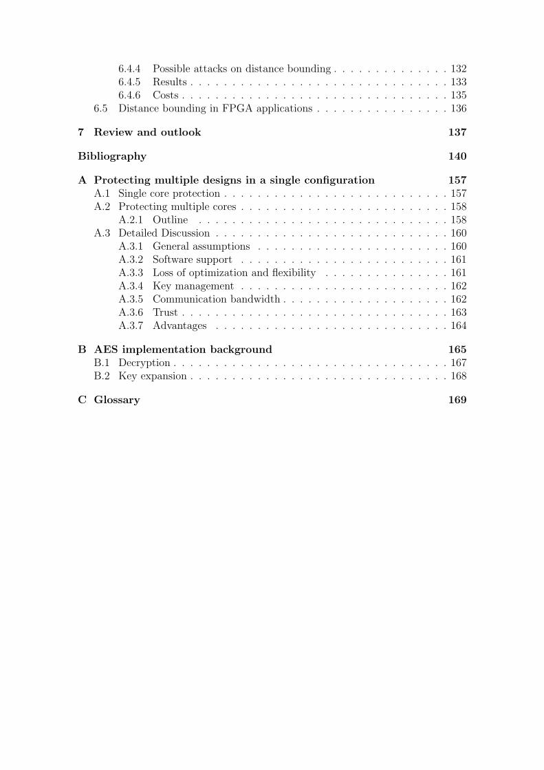
7 Review and outlook 137
Bibliography 140
A Protecting multiple designs in a single configuration 157A.1 Single core protection . . . . . . . . . . . . . . . . . . . . . . . . . . . 157A.2 Protecting multiple cores . . . . . . . . . . . . . . . . . . . . . . . . . 158
A.2.1 Outline . . . . . . . . . . . . . . . . . . . . . . . . . . . . . . 158A.3 Detailed Discussion . . . . . . . . . . . . . . . . . . . . . . . . . . . . 160
A.3.1 General assumptions . . . . . . . . . . . . . . . . . . . . . . . 160A.3.2 Software support . . . . . . . . . . . . . . . . . . . . . . . . . 161A.3.3 Loss of optimization and flexibility . . . . . . . . . . . . . . . 161A.3.4 Key management . . . . . . . . . . . . . . . . . . . . . . . . . 162A.3.5 Communication bandwidth . . . . . . . . . . . . . . . . . . . . 162A.3.6 Trust . . . . . . . . . . . . . . . . . . . . . . . . . . . . . . . . 163A.3.7 Advantages . . . . . . . . . . . . . . . . . . . . . . . . . . . . 164
B AES implementation background 165B.1 Decryption . . . . . . . . . . . . . . . . . . . . . . . . . . . . . . . . . 167B.2 Key expansion . . . . . . . . . . . . . . . . . . . . . . . . . . . . . . . 168
C Glossary 169
Published work
Of note are papers I have published in two of the top information security con-
ferences: “Keep your enemies close: distance bounding against smartcard relay
attacks” was published at USENIX Security Symposium 2007 and was the recipi-
ent of the “Best Student Paper” award; and, “Thinking inside the box: system-level
failures of tamper proofing” was published at IEEE Symposium on Security and Pri-
vacy (“Oakland”) 2008 and received the “Outstanding Paper Award” from IEEE
Security and Privacy Magazine. A poster based on the former has been chosen for
third place in a departmental competition, and participated in a regional poster
competition.
Listed below are my academic contributions while a research student:
Journal articles
S. Drimer, T. Guneysu, and C. Paar. DSPs, BRAMs and a pinch of logic: extended
recipes for AES on FPGAs (to appear). ACM Transactions on Reconfigurable Tech-
nology and Systems (TRETS), 3(1), March 2010.
S. Drimer, S. J. Murdoch, and R. Anderson. Failures of tamper proofing in PIN entry
devices. IEEE Security & Privacy Magazine, November/December Issue, 2009.
Book chapter
G. P. Hancke and S. Drimer. Secure proximity identification for RFID, chapter 9,
pages 171–194. Security in RFID and Sensor Networks. Auerbach Publications,
Boca Raton, Florida, USA, 2009.
Conference papers
S. Drimer and M. G. Kuhn. A protocol for secure remote updates of FPGA con-
figurations. In Reconfigurable Computing: Architectures, Tools, and Applications
(ARC), volume 5453 of LNCS, pages 50–61. Springer, March 2009.
S. Drimer, S. J. Murdoch, and R. Anderson. Optimised to fail: card readers for
online banking. In Financial Cryptography and Data Security, February 2009.
S. Drimer, S. J. Murdoch, and R. Anderson. Thinking inside the box: system-
level failures of tamper proofing. IEEE Symposium on Security and Privacy, pages
281–295, IEEE, May 2008.
S. Drimer, T. Guneysu, and C. Paar. DSPs, BRAMs and a pinch of logic: new
recipes for AES on FPGAs. In IEEE Symposium on Field-Programmable Custom
Computing Machines. IEEE, April 2008.
8
S. Drimer and S. J. Murdoch. Keep your enemies close: distance bounding against
smartcard relay attacks. In USENIX Security Symposium, pages 87–102, USENIX
August 2007.
S. Drimer. Authentication of FPGA bitstreams: why and how. In Reconfigurable
Computing: Architectures, Tools, and Applications (ARC), volume 4419 of LNCS,
pages 73–84. Springer, March 2007.
Online and technical reports
S. Drimer, T. Guneysu, M. G. Kuhn, and C. Paar. Protecting multiple cores in a
single FPGA design, May 2008.
http://www.cl.cam.ac.uk/~sd410/papers/protect_many_cores.pdf.
S. Drimer. Volatile FPGA design security – a survey (v0.96), April 2008.
http://www.cl.cam.ac.uk/~sd410/papers/fpga_security.pdf.
S. Drimer, S. J. Murdoch, and R. Anderson. Thinking inside the box: system-level
failures of tamper proofing. Technical Report UCAM-CL-TR-711, University of
Cambridge, Computer Laboratory, February 2008.
http://www.cl.cam.ac.uk/techreports/UCAM-CL-TR-711.pdf.
9
Work done in collaboration
Chapter 3 on secure remote updates is based on a paper co-authored with Markus
Kuhn who significantly contributed to the presentation and robustness of the pro-
tocols, especially in the support of multiple update policies.
In Chapter 4 on AES implementations, Tim Guneysu proposed the structure for
fitting AES into specific embedded functions of the Virtex-5 architecture and was
instrumental in discussing the design choices. Tim generated the T-table content
of the BRAMs and implemented the key schedule and counter mode of operation,
described in Sections 4.3.4 and 4.5.2, respectively. Otherwise, the implementations
are entirely my own.
Discussions with Markus Kuhn on reproducible research motivated the related
ideas presented in Chapter 5.
Chapter 6 on relay attacks and distance bounding is based on a paper co-authored
with Steven J. Murdoch, who developed the PC software tools that interface with my
custom hardware. Both Steven and Markus Kuhn have contributed to the design
choices required for adapting the Hancke-Kuhn distance bounding protocol to a
wired implementation, though the implementation is entirely my own.
10
Chapter 1
Introduction
A “gate array” is an integrated circuit (IC) consisting of a transistor grid fabri-
cated on a silicon wafer. Different arrangement of interconnect metal layers can be
added in order to define the function of the circuit, allowing the same mass produced
wafers to be used for performing different logic functions. Thus, gate arrays are one-
time programmable with limited integration, but are cheaper to manufacture than
custom-made application specific integrated circuits (ASIC). “Field programmabil-
ity” is the property that allows the functionality of a device to be modified in the
field, outside of the factory. Adding this property to gate arrays gives us field pro-
grammable gate arrays (FPGA), generic semiconductor devices that are made of
an interconnected array of functional blocks that can be programmed, and repro-
grammed, to perform virtually any user-described logic functions within the limits
of the resources it contains.
Gate array programmable logic devices (PLD) from the late 1970s (e.g., PLAs,
PALs, GALs) preceded what we know today as FPGAs, although when FPGAs
became available in the mid 1980s they were the first SRAM-based PLDs, highly
integrated, and volatile. Until the late 1990s, they were used mainly as interface
“glue logic”, while the largest FPGAs were, and still are, used for ASIC prototyping
and verification. Additionally, FPGAs could not have competed with ASICs on
price for the performance they provided, so their application space was limited and
they usually were not the main processor of a product.
In the past decade this has changed. Since the late 1990s, with the introduction of
what FPGA manufacturers call “platform FPGAs” and “systems on a programmable
chip”, FPGAs have increasingly included functions that previously required other
discrete ICs. 2009’s FPGAs have embedded processors, gigabit serial transceivers,
analog-to-digital converters, digital signal processing blocks, Ethernet controllers,
substantial memory capacity, and other functional blocks, such as clock managers
and multipliers, for performing a range of commonly required functions. In recent
FPGA generations we also see application-specific subfamilies that offer different
11
arrangements and concentration of functional blocks for particular sets of applica-
tions, such as DSP, military, automotive, or communication. This means that the
application space of FPGAs has widened as they became more capable, and that
designing with FPGAs now requires specialization, as they are no longer just an
array of simple logic blocks.
In terms of performance and power consumption, FPGAs are usually inferior
to ASICs1, but compete by being readily available, reprogrammable, and manufac-
tured using the latest technologies. They provide an appealing alternative where
the resources (cost, know how, time) required for ASIC development are not avail-
able. Against application-specific standard products (ASSP) – devices that perform
a fixed set of functions – FPGAs compete by being reprogrammable and by being
able to perform a variety of digital functions, not only those that are preset. The
ability to parallelize operations and execute customizable functions also makes their
performance competitive compared to sequential microprocessors.
In terms of security, the growth of FPGA capability and application space has
two main implications. Firstly, FPGA designs represent a significant investment that
requires protection; and secondly, FPGAs are increasingly being used in applications
that require FPGA security properties that are either unavailable today, or that
have yet to be adequately investigated. Thus, we may see increased attention to the
security attributes of FPGAs as more of them are used in the military, automotive
and consumer industries, each having their own security requirements.
In the academic community, “FPGA security” research has been steadily increas-
ing since the late 1990s, though the intersection of two significantly different fields
– engineering and security – has been problematic. This may be because security is
not a traditional engineering “problem” in that it does not have specifications that
can be shown to have been met. That is, a system is not proven to be more “secure”
simply because it has been implemented and shown to “work”. What we sometimes
see are published security schemes that appear to work, but exhibit subtle security
flaws, and ones that have sound security proposals but are impractical to implement
or incomplete (see for example Sections 2.3.1 and 2.3.5.2).
1.1 Motivation and contribution
This dissertation sets out to examine the role of FPGAs within a security system and
consider how solutions to security challenges, unique to the FPGA usage model, can
be provided. The term “FPGA security” includes the secure operation of designs
1In 2006, Kuon and Rose [116] estimated that on average FPGAs are roughly forty times larger,three times slower, and consume twelve times more dynamic power compared to ASICs, thoughFPGA vendors have recently been focusing on designing low power-consuming FPGAs, so themargins may have narrowed.
12
running within the FPGA; the secure delivery of configuration content to FPGAs;
the use of FPGAs for enhancing the security of systems; and, the use of FPGAs
as an adversarial tool. The contributions in this dissertation fall within these cate-
gories. Additionally, security analysis without context of where and how the target
of evaluation is used can lead to insecure systems. Thus, another important theme
of this dissertation is to provide context for the security analysis of reconfigurable
systems.
Chapter 2 is based on “Volatile FPGA design security – a survey” [51], which I
have written over the course of my time as a research student2. It seems to have be-
come a reference for those entering the field and has also motivated new research by
others (Badrignans et al. [20], for example). Also in Chapter 2, I include a summary
of “Authentication of FPGA bitstreams: why and how” [50], which evaluates the
merits of bitstream authentication – an essential building block for secure systems.
Chapter 3 is based on “A protocol for secure remote updates of FPGA configura-
tions” [54], which describes the first practical and secure remote-update protocol of
FPGA configurations that can work with existing FPGAs. Chapter 4 is based on
“DSPs, BRAMs and a pinch of logic: new recipes for AES on FPGAs” [56, 60], and
describes new ways to implement the AES block cipher on Virtex-5 FPGAs. These
can be used for encryption, decryption and message authentication code generation,
integral parts of security systems.
One of the AES variants presented in Chapter 4 is the fastest FPGA AES imple-
mentation reported in the academic literature. In that context, I argue in Chapter 5
that the performance of FPGA designs can vary significantly under different imple-
mentation conditions, and discuss the importance of having the ability to reproduce
implementation results, so that better comparisons to prior work can be made. This
discussion is especially pertinent in the context of competitions for cryptographic
primitives such as for the AES and the SHA-3, where comparison issues can have
an impact on the choice of candidates.
Chapter 6 is based on “Keep your enemies close: distance bounding against
smartcard relay attacks” [55], and describes the first secure distance bounding im-
plementation. The flexibility of FPGAs was crucial here, as programmable delays
and hand placement of circuit elements enabled the use of routing with specific de-
lays. Chapter 6 also demonstrates how FPGAs can be used as an adversarial tool
in a successful man-in-the-middle attack on a smartcard-based payment system. It
also discusses how man-in-the-middle attacks can violate assumptions made in the
design of reconfigurable systems.
I also include in Appendix A a discussion of how to protect multiple cores –
2The survey has been available online since October 2007, and was updated several times since. Asa companion to the survey, I also provide a comprehensive “FPGA design security bibliography”as a resource for the community [52].
13
from mutually distrusting contributors – that are integrated into a single FPGA
design so to enable a “pay-per-use” cores distribution model. The idea is described
qualitatively, exploring its feasibility in the context of trust between principals,
additional configuration logic circuitry, and communication bandwidth.
1.2 Reading this dissertation
For material that can be easily found on an organization’s website using a document
identifier, I reference the organization and indicate the identifier in the citation. A
reference to the NIST AES specification, for example, appears as [139, FIPS197]. A
shorthand notation for document types is also used: UG (user guide), WP (white
paper), DS (data sheet), TN (technical note), AN (application note), and SP (special
publication); for pointers within a document, p (page), ch (chapter), and t (table)
are used. A reference to page 7 of Altera Application Note 357, for example, appears
as [7, AN357, p7].
Some references to online news articles and webpages are given as a URL together
with the title, and there is a chance that some will eventually become invalid. Thus,
the URL references are chosen to not detract from the point that is being made
if missing; if a dead link is found, there is always the possibility of finding the
information by searching the Internet or looking for it on the WayBackMachine
(http://www.archive.org/).
Finally, I sometimes include extra information in text boxes (such as the one the
next page). These are written informally and usually contain insights, unfinished
thoughts, or interesting anecdotes that are related to the material I discuss. The
content of these boxes is not crucial for the understanding or flow of the text, so
they can be safely ignored.
14
Personal motivation. I became intrigued by the security aspects of FPGAsduring lunch with a few senior engineers as a “new college graduate” working forXilinx. One of them asked my boss if we had a true random number generatorfor FPGAs; my boss said “no” and I intervened with “possibly”, rememberingsome seemingly random behavior of a circuit I was working on. I was able tocreate a true random number generator out of this circuit [53], and started toexplore what else is available under the general topic of “FPGA security”. Backthen, 2003-2004, I found Wollinger et al. [185] to be a good survey, but thoughtthat it did not exactly satisfy what I was looking for: a comprehensive study ofthe unique problems of distributing content to FPGAs and how to ensure secureoperation. I was also looking for a readable reference for industry engineers. Istarted working on security related projects within Xilinx for the next couple ofyears, learning as I went along, eventually embarking on the PhD adventure atCambridge in October 2005.I began writing “Non volatile FPGA design security – a survey” shortly afterI had started the program, and had found that much of the material I wasreading did not fit well with the world view I had of where and how FPGAsare used; essentially, my industry view clashed with the academic one. I havesince observed that the reason was that many of the contributions were eithermade by “security people” working with FPGAs, or “FPGA people” exploringdesign security. With my background I wanted to position myself as someonethat can do both reasonably well. One of the goals of my survey was to providea framework and common terminology for others to use as the basis of theirresearch, so that there is background material already set. The goal of thisdissertation is similar, with my own contributions in the areas where I thoughtsolutions, or other perspectives, are needed.
15

16
Chapter 2
FPGA security foundations
“FPGA security” is an intersection of two rather different fields, and I anticipate
a variety of audiences: experienced security or FPGA professionals, and computer
scientists or engineers with little background in either. Authoring a document that
would keep all of them constantly intrigued is impossible, so I try to balance the
discussion. Where I use cryptographic primitives I will not discuss their finer details
– except for Chapter 4 on AES implementations – and refer the interested reader to
Anderson [10], Menezes et al. [134], and Schneier [150].
For those who are not expert FPGA users, I think that the content of this chapter
is sufficiently detailed in order to appreciate the work described in later ones; for
a recent and comprehensive FPGA architecture survey, I refer the reader to Kuon
et al. [117]. I take this opportunity, however, to both introduce the basic mode of
operation of volatile FPGAs, and the terminology I use throughout the dissertation
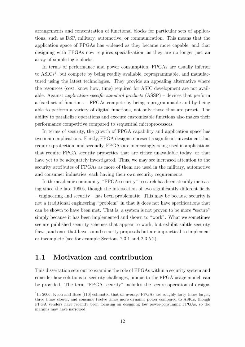
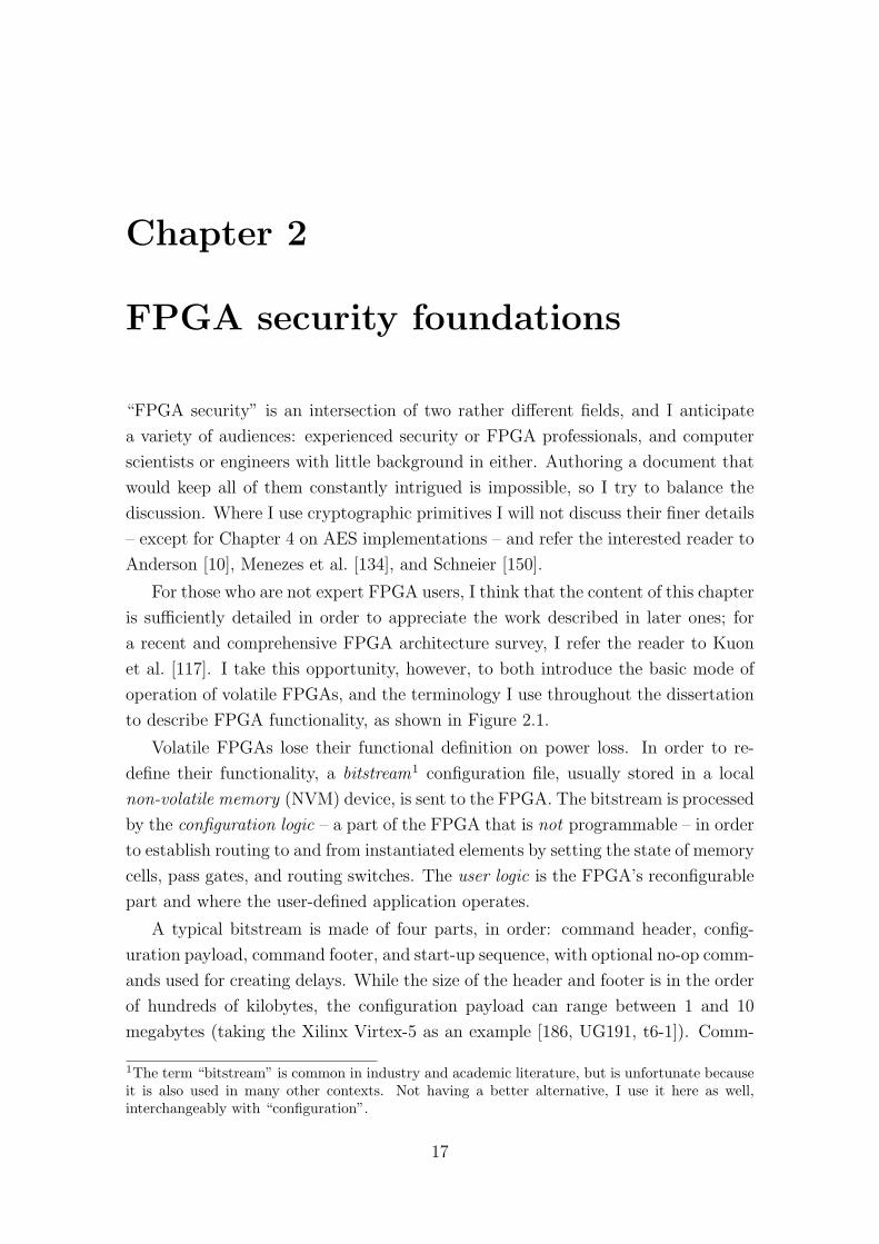
to describe FPGA functionality, as shown in Figure 2.1.
Volatile FPGAs lose their functional definition on power loss. In order to re-
define their functionality, a bitstream1 configuration file, usually stored in a local
non-volatile memory (NVM) device, is sent to the FPGA. The bitstream is processed
by the configuration logic – a part of the FPGA that is not programmable – in order
to establish routing to and from instantiated elements by setting the state of memory
cells, pass gates, and routing switches. The user logic is the FPGA’s reconfigurable
part and where the user-defined application operates.
A typical bitstream is made of four parts, in order: command header, config-
uration payload, command footer, and start-up sequence, with optional no-op comm-
ands used for creating delays. While the size of the header and footer is in the order
of hundreds of kilobytes, the configuration payload can range between 1 and 10
megabytes (taking the Xilinx Virtex-5 as an example [186, UG191, t6-1]). Comm-
1The term “bitstream” is common in industry and academic literature, but is unfortunate becauseit is also used in many other contexts. Not having a better alternative, I use it here as well,interchangeably with “configuration”.
17

configurationpayload
headerfooter
start-up sequenceFPGA
user logic
processing
NVM
configuration logic
bit-stream
application
Figure 2.1: A volatile FPGA requires a configuration file to define its functionality. Theconfiguration logic processes this file so to set the user logic to perform user definedfunctions. A complete bitstream includes a header with configuration instructions followedby a payload and footer, which includes the start-up sequence to activate the FPGA.
ands are 32 bits wide and control various aspects of the FPGA configuration options.
Header commands, for example, tell the configuration logic which configuration
mode to use (serial, parallel, etc.), whether the payload is encrypted, whether to
disable readback, or when to assert the global signals that prevent contention during
configuration. The footer contains commands to check the integrity of the bitstream
(by comparing the bitstream CRC checksum with a precalculated value), and a series
of instructions for starting up the FPGA with the new configuration.
2.1 FPGA usage model
2.1.1 Principals
“A principal is an entity that participates in a security system. This entity can be
a subject, a person, a role, or a piece of equipment, such as a PC, smartcard, or
card-reader terminal” [10, p12]. FPGAs, FPGA vendors, engineers, configuration
programming controllers, etc. are principals interacting within a security system;
understanding their limitations and interests is important for any security analysis.
The principals that comprise the design and distribution of FPGA-based systems
are introduced below.
FPGA vendor. Three FPGA vendors dominate the volatile FPGA market: Al-
tera, Lattice and Xilinx – each introducing a new family of FPGAs roughly every 12
to 18 months. FPGA vendors have two primary security concerns. Firstly, protect
their own proprietary designs and technology from being reverse engineered, copied,
or modified. And secondly, provide their customers ways to protect their designs
throughout the development flow and in the field. FPGA vendors also have an incen-
tive to facilitate secure integration and distribution of design modules from multiple
sources in order to to stimulate that market, which leads to increased FPGA sales.
The recent availability of volatile FPGAs that target security applications (such as
18

Cyclone III LS and Spartan 3AN) reflects demand, and may indicate that security
has become a competitive factor.
Understanding the mindset of FPGA vendors is important when we suggest
architectural and logistical changes to how FPGAs are used. My own experiences
working for an FPGA vendor suggest that the following considerations play an
important role when new features are evaluated.
• “Transistor count” as a sole criterion for cost evaluation can be misleading be-
cause it does not take into account verification (pre-fab simulation), character-
ization (post-fab testing), and production testing costs. Characterization and
verification require significant amount of engineering hours, even for simple cir-
cuits, while production testing requires “IC testers” that may cost millions of
dollars and are expensive to operate. Each engineer-hour and tester-milli-second
is factored into the cost of adding a circuit to the FPGA (more in box on this
page). The contribution of this circuit must be justified by future returns. Thus,
transistors can be expensive (i.e., not “free”).
• “Unreliable” circuits are unlikely to be added as hard functions. For example, it
is sometimes useful for some security applications to have the ability to perma-
nently disable a device (i.e., “kill switch”), or to have an embedded true random
number generator. However, the former increases support costs, opens the FPGA
to denial of service attacks, and can have an effect on reputation if reliability is
questioned. Similarly, it is notoriously difficult to guarantee reliable operation
of true random number generators under all environmental conditions. So even
if a function is efficient, compact, and useful, it may still not be adopted.
• The price of a single FPGA chip is not a function of the amount of resources that
are being used. Every FPGA type has several family members, each having a
fixed number of resources. System developers can only purchase FPGAs in fixed
sizes, so any unused resource is a loss for them. Therefore, FPGA vendors design
each embedded function such that it provides utility to the largest amount of
users. The view of FPGA vendors, it seems, is that if developers want to use an
FPGA in an “out of the ordinary” way, they will need to pay for it (by using
larger FPGAs or additional peripheral devices).
Testing is expensive. If the tester-time argument still seems unconvincing,consider what Xilinx does with EasyPatha; they seem to sell FPGAs at a sig-nificant discount if they only fully test the parts of the FPGA that the designeruses, and at the application’s maximum frequency, not of the FPGA’s.
ahttp://www.xilinx.com/products/easypath/
19
Foundry. All current FPGA vendors are fabless – they design the FPGAs but
other companies, “foundries”, manufacture them. Foundries are principals on their
own right since they play a crucial role in the security of FPGAs, as it is possible
that designs are modified or stolen while in their possession. If cryptographic keys
or serial numbers embedded in the FPGA by the foundry are compromised, then
that may undermine the application’s security. Until the late 1990s it was still
economically viable to maintain “trusted foundries” in the country where the devices
were designed (mainly the United States). Today, most advanced foundries are in
Asia, where oversight by foreign governments is not likely to be possible. In a
2005 report [177], the U.S. Department of Defense discusses the “alarming” rate at
which “critical” microelectronics facilities are migrating to foreign countries. More
recently, the U.S. DoD has allocated many resources for researching detection of
malicious circuits, or any deviation from the original design [2]. Researchers for the
Australian Department of Defence also indicate that the “curious arrangement” of
sourcing low-level components for critical infrastructure from potential adversary
countries, makes “silicon Trojans” an attractive proposition [9, p3]. More on this in
Section 2.1.4.
System developer. FPGA vendors sell FPGAs, often through distributors, to
system developers who use them in their product. System developers fall into two
groups based on their security needs and views.
• Cost-conscious. The goal of commercial designers is to meet product specifica-
tions at the lowest cost. Most often, there is a performance/cost trade-off and
a tendency to avoid any additional components, delays, maintenance, support
and so on, all of which lead to increased costs. The life-cycle of a commercial
product can be quite short, from months to a few years, so designs may only
need to be protected for that long. An “old” product is not a worth-while target
for attackers, and even if it was, the resulting losses may no longer be significant.
Commercial product designers are often concerned about cheap counterfeits com-
peting with the original product. Therefore, it is sometimes sufficient to make
the process of stealing the design at least as costly as re-inventing it (or slightly
harder to copy than a competing product).
• Security-conscious. Government contractors and security-industry system devel-
opers are concerned with protecting designs, methods of operation, and commu-
nications for long periods – from years to decades – while cost considerations
may be secondary if those imply security compromises. The security-conscious
designer is often interested in robust “approved” security mechanisms, based
on established protocols and algorithms. Some security-conscious designers use
20

older and mature integrated circuits, which are seen as more reliable. Others
take advantage of more recent technologies that are seen as more resistant to
probing (“invasive”) attacks, and with a higher entry threshold for adversaries
because of high equipment costs and required expertise.
FPGA vendors, therefore, have a challenge: in a resource-limited device, they
would (ideally) like to satisfy both cost- and security-conscious designers, who have
significantly different views on security, and what they are willing to spend on it.
EDA software vendor. Electronic design automation (EDA) tools are used for
the development of printed circuit boards, integrated circuits, FPGA designs, and
they are extensively used for simulation, among many other applications. The var-
ious EDA vendors provide the tools that are used by all the principals mentioned
above with FPGA vendors also being EDA tool suppliers themselves. Therefore,
EDA software vendors play a pivotal role in the FPGA design flow and their con-
tribution is critical to the security of both the FPGA and FPGA-based products.
Cores designer. Cores2 are ready-made functional descriptions that allow system
developers to save on design cost and time by purchasing and integrating them into
their own design. A single “external” core can also occupy the entire FPGA to
create a virtual application-specific standard product (VASSP; a term first used for
this purpose by Kean [103]). Cores are sold as hardware description language (HDL)
modules or as compiled netlists. Some are also available freely from FPGA vendors
(who profit from selling the FPGAs) and from Internet sites such as OpenCores3.
Today, there exist free or commercial cores for many commonly required logic and
cryptographic function.
System owner. The system owner (or current holder) possesses the FPGA-based
system, and may be a user who purchased the system at a shop, or a government that
obtained it from a fallen reconnaissance aircraft; both may be considered malicious
(“the enemy”), trying to pry secrets out or circumvent security. While in the hands
of the owner, the system developer has restricted or no control over the system.
The developer may try to restrict the owner from using certain functions aiming to
prevent theft of services, execution of “unauthorized” code, or to price-discriminate.
2I use the following definitions for types of cores. “Hard cores” refer to embedded functionsin the non-reconfigurable part of the FPGA. “Soft cores” are HDL modules, with a distinctionbetween generic and architecture-specific cores. The former is portable and synthesizable to anyarchitecture, so not optimized, while the latter uses specific properties of the target architecturefor better performance. Here, “cores” will mean architecture-specific ones; otherwise, I will use“generic cores”. Finally, “firm cores” refers to cores with properties between “hard” and “soft” andcan mean an encrypted core or one with limited portability; to avoid confusion I will be specific.3http://www.opencores.org/
21

packagingFPGA vendor foundry
softwareflow
maskfiles
designfiles
maskfiles
fabricationprocess
wafer FPGA
die
pack-age
FPGA
FPGA vendor
distribution
final testing
Figure 2.2: Simplified FPGA design, manufacturing, packaging, and testing processes.
For example, some set-top box developers profit from providing programming ser-
vices, not from supplying the hardware itself, so have the incentive to invest in
mechanisms that prevent theft of these services. Some mobile phone manufacturers
have mechanisms to prevent users from using a network other than the one they are
“supposed” to be locked into. The security-conscious designer may also want to have
a way to completely erase or destroy portions of the system when it falls into the
“wrong” hands and perhaps employ the ability to “call home” when tampered-with
as a sign of distress (a radio carried by a soldier in the field, for example).
System manufacturer. The system developer does not usually have the ability to
mass produce a product, so designs are sent to a system manufacturer for production
and often also for testing. This principal includes all parties involved in the process
of making the system ready for delivery: printed circuit fabrication, assembly (where
components are soldered onto the board), testing, and packaging.
Trusted party. Some security protocols require a principal that is trusted by all
other principals in order to maintain particular security properties (storing, gener-
ating, processing and transferring of data and keys, for example). It is quite easy to
add a trusted party to a protocol, though establishing a mutually trusted principal
in practice can be challenging. The centralized nature of a trusted party makes it
vulnerable to denial of service attacks, and a lucrative target for attackers. Addition-
ally, practical issues such as location, trusted personnel, physical security, liability,
insurance, governance, auditability, and so on can be problematic and expensive.
2.1.2 Design and manufacturing flow
Figure 2.2 shows a simplified manufacturing process of an FPGA. HDL design files
are processed by software tools that produce a netlist that is laid-out, providing
22

fieldedsystem
fieldreconfiguration
external IP
cores designer
systemdevelopment
system developer
systemmanufacturing
manufacturingfacility
FPGA
softwareflow
bit-stream
HDLcode
bit-stream
NVM
FPGA
system owner
network
bit-stream
NVM
FPGA
HDL or netlist
Figure 2.3: The development, manufacturing, and distribution of an FPGA-based system.The system developer must be assisted by several other principals such as manufacturers,and cores and EDA vendors. At the end of the development cycle the product is in thesystem owner’s hands.
synthesis
HDL netlist placelist bitstreammap/fit,
place & route encoding
functional simulation static timing analysis
Figure 2.4: Expanded view of the software flow used to process a functional description ina high-level language into a bitstream file that is programmed into the FPGA to have itperform this functionality.
the design’s physical representation as transistors and metal interconnects. From
the layout, “mask sets” are sent to a foundry where they are turned into physical
“wafers”. (This is a simplification; several other principals other than the foundry
may be involved in the process.) The wafers are then tested for good dice and then
sent for assembly where those are cut and embedded in a carrying package. Finally,
these packaged dice are sent back to the FPGA vendor for final testing before they
are shipped to distributors and developers.
Figure 2.3 shows the design and manufacturing processes of an FPGA-based
system. It is not a complete description, but is meant to indicate where the prin-
cipals interact. In the development phase, the system in which the FPGA operates
is developed, and the developer combines internally- and externally-designed cores
23
that describe the FPGA logical function. The software flow, as shown in Figure 2.4,
begins with HDL synthesis that optimizes and translates the functional description
according to the resources available in the target FPGA architecture (e.g., Stratix
look-up table, Spartan multiplier, etc.) into a netlist. Netlists describe instanti-
ated primitives and the connections between them, often in the electronic design
interchange format (EDIF). Several EDA vendors offer synthesis tools, including
the FPGA vendors themselves, though the post-synthesis flow is nearly always per-
formed by proprietary FPGA vendor tools. Netlists are then mapped/fitted to
primitives in the target architecture and then those are placed and routed (PAR) to
a particular target device to produce a placelist4, where the specific placement and
routing of every interconnect and physical placement of all primitives is described.
Placelists are encoded into bitstreams that configure the FPGA to perform the log-
ical function initially described in HDL. As SRAM FPGAs are volatile, they must
receive the bitstream on every power-up from an external source, usually a non-
volatile memory device, EEPROM or Flash, placed nearby on the circuit board.
Designs are simulated at the HDL, netlist, and post-PAR stages, and can also
be verified for correct operation when “executed” on the FPGA itself in its intended
hardware setting5. Static timing analysis takes into account the architecture and
actual delays after the place and route process in order to verify that timing vio-
lations, such as of setup and hold tolerances, do not occur. When the prototyping
process is done, the system is manufactured and tested before being shipped. In the
field, the product is in the hands of the system owner and thus, no longer under the
developer’s control, though he can still perform field reconfiguration if the system is
capable. For example, a firmware upgrade to a digital camera may be done remotely
by the owner by plugging it into an Internet-connected PC, or an upgrade to a car
processor may be done by a service technician at a garage.
2.1.3 Defense categories
The effectiveness of a defense mechanism is evaluated by the cost of circumventing
it and how well it copes with the incentives of attackers. The cost of acquiring skill,
tools, and time required for “breaking” the defense give analysts a metric for the
system’s estimated level of security. I define the following defense categories.
• Social deterrents are laws, peoples’ good social conduct and aversion from being
prosecuted and punished. Designs can be protected by non-disclosure agree-
ments, trademarks, copyrights, trade secrets, patents, contracts, and licensing
agreements, often summed up by the term “intellectual property” (IP)6. How-
4I coin this new term here in order to make sure that the difference between traditional netlistsand placelists is clear.5With tools such as “SignalTap” by Altera [7, AN323] and “ChipScope” by Xilinx [186, UG029].6I try to avoid this overloaded catch-all term in favor of other, more descriptive, terms.
24
ever, social deterrents are only effective where appropriate laws exist and are en-
forced. Attitudes towards design-ownership rights vary significantly worldwide,
making this type of deterrent not wholly effective in places where it matters the
most: countries that source counterfeit goods tend to be places where design
ownership rights laws and enforcement are weak or ambiguous.
• Active deterrents are physical and cryptographic mechanisms that prevent theft
and abuse of designs. Active protection is highly effective if implemented correct-
ly, and is also locale-independent (if we ignore export restrictions). Further,
combined with social deterrents, active deterrents can help convince a court that
the designer has taken appropriate measures to protect a design and that the
perpetrator showed significant malicious intent by circumventing them.
• Reactive deterrents provide detection or evidence of breaches, which may help
in applying available social tools. Digital forensics relies on video surveillance,
fingerprinting, and steganography, etc., for initiating investigation or improving
the security of a system after a breach. Audit trails are reactive, but are also
an important facet of security in the absence of, or in addition to, active ones.
Reactive measures do not actively prevent fraud or theft, but their presence may
deter would-be attackers, and it can be beneficial to advertise them.
2.1.4 Trust and trustworthiness
How can users of software and hardware be confident that the tools they use are
“honest”, and not covertly inserting malicious code or circuits into their products?
Software and chip verification is an option, but usually prohibitively costly. The
sheer enormity of EDA tools make this impractical even if we assume that EDA
vendors made their source code available for scrutiny. Further, how can one be
sure that the source code compiler or simulator are trustworthy? In Reflections on
trusting trust, Thompson [170] elegantly discusses these issues and concludes that
“you can’t trust code that you did not totally create yourself. . . No amount of source-
level verification or scrutiny will protect you from using untrusted code”. Verifying
integrated circuits is even harder than software verification, especially so without
access to the design files and a complete audit along the manufacturing process.
Some may rely on knowing that companies want to build and maintain a positive
reputation: being honest, technologically advanced, quality-driven, etc., which is an
asset that is slowly gained, but easily lost. By striving to maintain such reputation,
companies are aligning themselves with the interests of their customers (assuming
a competitive market). Many millions of dollars are invested in designing and man-
ufacturing an FPGA family, and it is in the interest of both FPGA vendors and
foundries that these do not go to waste. This requires many self-enforced check-
points to ensure that no flaws or deviations from the intended design are made.
25

For example, the foundry must deliver high-yielding wafers that perform (only) the
original design, and in turn, FPGA vendors need to provide their customers reliable
FPGAs that correspond to data-sheets7.
“Silicon Trojans” are increasingly gaining attention in the defense [2, 9, 177] and
research [109] communities8. Developers may rely on the “scatter gun” [9] nature
of FPGA; that is, attackers do not know where the “Trojan inside” devices end up
and must create a discovery mechanism, increasing the likelihood of detection. If
the Trojan relies in any way on certain user logic functions being used, the likeli-
hood of discovery is further reduced. Concerned developers can purchase devices
manufactured at different foundries, or of different batches in order to decrease the
likelihood of a targeted attack. That said, Thompson showed us that we can always
step back: what if an IC FPGA designer consistently inserts malicious circuits into
the circuit designs? What if the EDA tools used for IC design insert these circuits?
The silicon Trojan problem is an interesting and timely one, but outside the scope
of this dissertation.
2.1.5 Distribution security
“FPGA security” can be divided into two categories: “operational” and “distribu-
tion”. Operational security is where we want to secure systems already running
inside of the FPGA. Distribution security is how to get these designs to the FPGA
while maintaining certain security properties.
We may consider distribution security as the following three categories. The first
is securing configurations from local storage (a PROM, for example) in a hostile
environment, as will be discussed in Section 2.3.1. The second is securing remote
configuration updates, as will be discussed in Chapter 3. The third is maintaining
the confidentiality and authenticity of individual cores from multiple sources, which
are integrated into a single design.
Consider a multimedia device startup company that developed a clever way for
implementing an H.264/MPEG-4 AVC encoder/decoder. They would like to add
USB and encryption support to their devices so they license AES and USB 2.0 cores
developed externally. In the absence of an industry standard, FPGA vendors created
their own solutions for allowing potential users to evaluate these external cores.
Altera, for example, allows non-Altera cores hosted on its website to be compiled and
evaluated for resource use, but its software does not allow bitstream generation from
these [7, AN343]. For its own cores, Altera software creates time-limited bitstreams
7ASIC design and manufacturing has similar problems, but FPGAs have the advantage of beinggeneric such that tampering may be detected with higher probability simply because of the largeruser-base.8The “Hardware-Oriented Security and Trust” (HOST) IEEE workshop is dedicated to the topic,http://ieeexplore.ieee.org/xpl/tocresult.jsp?isnumber=4559030.
26

(“untethered”), or ones that require continuous connection between the FPGA and
the development software through a programming cable (“tethered”), so designs can
be tested on-chip [7, AN320]. Xilinx allows evaluating of some cores for embedded
processors that expire after “6–8 hours when running at the nominal clock frequency
specified for the core” [187], while other HDL cores are available through various
licenses that allow a time-limited evaluation. Both Altera and Xilinx schemes require
that users agree to restricted use of the cores, and likely rely on the bitstream’s
encoding, not cryptography, for enforcing the timing restrictions while the cores are
operating inside the FPGA.
Our startup may have been able to evaluate the cores, but is faced with only one
choice for purchasing them: pay a “blanket license” for unrestricted use of the cores.
Such licenses can be prohibitive for the startup, especially since they do not know
how successful their product will be. Even if they can afford such a license, they
may not actually be sold one. The “design-reuse” industry has dealt with secure
distribution of cores by mostly relying on social constructs such as “trusted partners”
and reputation as we discussed in Section 2.1.4. An industry-wide panel discussion
in early 2007 [183, 184] provides some insight into the industry’s perception of using
a software encryption flow for cores protection. They concluded that the current
trust-based system is working well for large corporations – less so for startups – and
a better solution is desirable for the long-run, but is not necessarily urgent (note
that the focus is on ASIC cores, so the unique FPGA usage model is not considered
carefully). What this may mean is that cores vendors have a risk perception, and
may choose not to sell to non-established companies who have no reputation to lose,
or ones that are based in particular countries.
For small companies, we probably need to create a distribution system that does
not rely on social deterrents, and that allows developers to integrate cores from
multiple sources into their design, but still only pay on a per-use basis. Encrypted
netlists are one solution, already supported by some EDA vendors, though it may be
too cumbersome or even insecure (see the box on the next page). Therefore, I argue
that if we rely on hardware-based protection mechanisms that operate at the design
flow’s final stages, we are likely to better resist attacks. Appendix A discusses the
merits of one possible solution I propose.
2.2 Usage model attacks
Security is an arms race; in a typical cycle, incremental defenses are put in place
as older defenses are overcome and new attacks emerge. Smartcards and micro-
controllers have been in the midst of such a race for the past two decades, start-
ing with naive, if present at all, security mechanisms and incrementally improv-
27
ing as exploits are discovered; examples are the work by Anderson, Kommerling,
Kuhn, and Skorobogatov [12, 13, 112, 157]; Anderson et al. [14] provide a survey
of cryptographic processors designed for security applications. But, compared to
typical FPGA applications, smartcards can have short life-cycles and are consider-
ably cheaper. Pay-TV smartcard hacking emerged in the 1990s when IC cards were
issued by service providers to combat subscription fraud. The usage model allowed
issuing new smartcards on a monthly basis, or the adding of a security feature in a
short development cycle, which is not possible for FPGAs. We may now be seeing
the beginning of such an arms-race for FPGAs, as they are used in applications
that require security (military, automotive), but also because designs are becoming
more valuable. Incentives are mounting for attackers to concentrate their efforts on
FPGA exploits.
Can a software-encrypted netlist flow withstand determined attack-ers? In June 2006, Synplicity proposed the “Open IP Encryption Initiative” forsecure core exchange [44] and offered it to the Virtual Socket Interface Alliance(VSIA) to become an industry standard. In June 2007 VSIA shut downa, and inApril 2008 Synplicity launched its initiative under the “ReadyIP” brand nameb.But Synplicity’s original Open IP proposal had made some poor security choices,such as the distribution of vendors’ private keys with each instance of the soft-ware. Barrickc argues against using encrypted netlists on practical grounds, butalso claims that sometimes they can be worth it in terms of savings.While these measures may keep “honest people honest”, how long will it takebefore the software is cracked on a “break once, run anywhere” basis? If thereis anything to be learned from the rich history of software protection failures, itis that very few copy protection schemes have withstood (determined) attack-ers [10, p681–688]. Perhaps there is a silver lining in encrypted flow: incentivesare aligned for better security. Varian [181] argued that security suffers if theprincipal in the position to improve it does not bear the loss due to breaches.Thus, if an FPGA vendor implements a design protection scheme for its owncores, or even for others’, and it fails, the vendor is the one who bears the loss(directly, or indirectly due to loss of reputation), so has an incentive to make itthe best it can be.
a“Legacy Documents of the VSI Alliance”, http://www.vsi.org/b“Synplicity Launches ReadyIP Program: The Industry’s First Universal, Secure IP Flow ForFPGA Implementation”,http://www.synplicity.com/corporate/pressreleases/2008/SYB-0026.htmlc“Designing Around an Encrypted Netlist: Is The Pain Worth the Gain?”,http://www.design-reuse.com/articles/18205/encrypted-netlist.html
28

2.2.1 Bitstream reverse engineering
I define bitstream reversal as the transformation of an encoded bitstream into a
(human readable and editable) functionally-equivalent description of the original
design that produced it. It is the reversal of the flow shown in Figure 2.4, from
bitstream back to HDL or netlist. Partial bitstream reversal is the extraction of
limited information from bitstreams – such as keys, BRAM/LUT content, or memory
cell states – without reproducing complete functionality. Full bitstream reversal
would allow replicating functionality (with a different looking bitstream); extracting
secret cryptographic keys; and proof of infringement (interestingly making both
criminals and developers interested in reverse engineering). Partial reversal helps
recovering hidden data, but may also reveal the types of cryptographic primitives
used and how they are implemented, which can enhance power analysis attacks.
The Virtex-5 Configuration User Guide [186, UG191] is quite revealing about
the structure of its bitstreams, compared with previous disclosures of the propri-
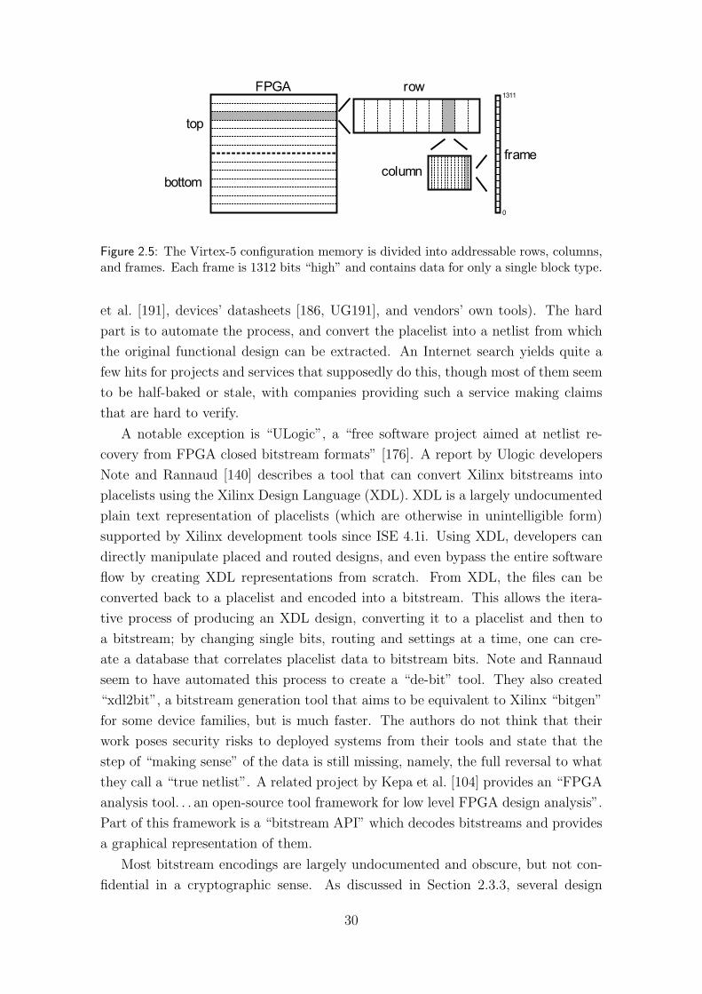
etary bitstream format, which is outlined in Figure 2.5. I will use this conceptual
simplification of the Virtex bitstream format when I discuss bitstream manipulation.
“Frames” are the fundamental configuration unit: a single-bit column of 1312
bits (41×32-bit words) that cover the entire FPGA. Each frame contains the config-
uration for one hardware primitive (configurable logic blocks, DSP, I/O blocks, block
RAM, etc.) and is addressable such that it can be written and read individually.
This allows, for example, partial reconfiguration, and detection/correction of upsets
due to ambient radiation using an internal configuration access port9.
Extracting RAM and LUT content from bitstreams is not difficult (see Ziener
9Primitive-specific frames were introduced for Virtex-4; earlier Xilinx FPGAs’ frames consisted ofconfiguration bits for several primitives which complicated these operations.
Bitstream reverse engineering background. In the early 1990s, the startupcompany NeoCAD created a complete FPGA development tool chain for a fewFPGA families. According to Xilinx [123, 172], NeoCAD managed to reverse en-gineer the bitstream generation executable in order to generate compatible bit-streams, rather than reverse engineer the bitstream format itself. In 1995 Neo-CAD was acquired by Xilinx to become its software division. In the late 1990s,the startup Clear Logic was able to use Altera’s software-generated bitstreamsto produce pin-compatible, smaller, cheaper, laser-programmable ASICs, whichwere also more secure since they did not require an external bitstream source.Altera sued and requested that Clear Logic cease operations. In 2001, a courtprohibited Clear Logic from asking its customers to use Altera’s software toolssince that violated its end-user license agreement (EULA). In 2003 Clear Logicclosed down, and in late 2005, Altera won the case [8, 178].
29
FPGA row
columnframe
0
1311
bottom
top
Figure 2.5: The Virtex-5 configuration memory is divided into addressable rows, columns,and frames. Each frame is 1312 bits “high” and contains data for only a single block type.
et al. [191], devices’ datasheets [186, UG191], and vendors’ own tools). The hard
part is to automate the process, and convert the placelist into a netlist from which
the original functional design can be extracted. An Internet search yields quite a
few hits for projects and services that supposedly do this, though most of them seem
to be half-baked or stale, with companies providing such a service making claims
that are hard to verify.
A notable exception is “ULogic”, a “free software project aimed at netlist re-
covery from FPGA closed bitstream formats” [176]. A report by Ulogic developers
Note and Rannaud [140] describes a tool that can convert Xilinx bitstreams into
placelists using the Xilinx Design Language (XDL). XDL is a largely undocumented
plain text representation of placelists (which are otherwise in unintelligible form)
supported by Xilinx development tools since ISE 4.1i. Using XDL, developers can
directly manipulate placed and routed designs, and even bypass the entire software
flow by creating XDL representations from scratch. From XDL, the files can be
converted back to a placelist and encoded into a bitstream. This allows the itera-
tive process of producing an XDL design, converting it to a placelist and then to
a bitstream; by changing single bits, routing and settings at a time, one can cre-
ate a database that correlates placelist data to bitstream bits. Note and Rannaud
seem to have automated this process to create a “de-bit” tool. They also created
“xdl2bit”, a bitstream generation tool that aims to be equivalent to Xilinx “bitgen”
for some device families, but is much faster. The authors do not think that their
work poses security risks to deployed systems from their tools and state that the
step of “making sense” of the data is still missing, namely, the full reversal to what
they call a “true netlist”. A related project by Kepa et al. [104] provides an “FPGA
analysis tool. . . an open-source tool framework for low level FPGA design analysis”.
Part of this framework is a “bitstream API” which decodes bitstreams and provides
a graphical representation of them.
Most bitstream encodings are largely undocumented and obscure, but not con-
fidential in a cryptographic sense. As discussed in Section 2.3.3, several design
30

protection schemes rely on the continued secrecy of these encodings, and vendors
seem to intend to keep it this way. The obscurity, complexity, and size of bitstreams
makes the reverse engineering process difficult and time consuming, though theo-
retically possible. The Ulogic project stated goal is the re-production of netlists,
and there are likely to be similar efforts that are not public. The possibility of le-
gal action can be an effective deterrent in academic and commercial environments,
although for some organizations or countries, these are less of a concern. The in-
creased value embodied in bitstreams may inevitably drive increasingly more people
and organizations to invest time in accomplishing automated full reversal. Such a
tool only needs to be created once before it can be used by others with little effort.
If reverse engineering is a concern, or thought to be within the capabilities of
potential adversaries, it seems prudent to no longer rely on bitstream encoding for
protection, even while the actual cost of full reversal remains unclear. Merely hiding
keys in look-up tables and RAM is not a good strategy: recovering those requires
only partial reversal and basic knowledge of the bitstream format. Future solutions
may best relay on cryptographic protection of designs rather than on bitstream
format obscurity; this view is reflected in the schemes I propose in Chapter 3 and
Appendix A.
2.2.2 Counterfeits
Where all FPGAs of the same family and size are identical, a bitstream made for
one device can be used in another. Because of that, attackers can, and do, clone
bitstreams by recording them in transmission to the FPGA and use them in simi-
lar systems or products, usually cheaper clones that are sold instead of, or as, the
originals. Since cloning requires no more than a logic analyzer and a competent
technician, it is very simple to perform. The attacker, who does not need to under-
stand the details of the design, regards it as a black-box, and only needs to invest
in copying the circuit board the FPGA is mounted on, saving development costs.
The original system developers have two main concerns with regards to cloning.
Firstly, cloned systems reduce profits after a significant development investment,
and secondly, if the clone is marked as the original, the system developer suffers a
reputation and support loss if the fake is of poor quality. Deterrents such as those
discussed in Section 2.3.3 aim to increase the cost of cloning, and may make cloning
unprofitable for low level attackers.
The electronic industry is losing out to large amounts of counterfeit hardware
that is either cloned or the result of overbuilding (“run-on fraud”) [6, 179]. When
a product is manufactured at a contracted facility that manufactures and tests the
hardware before it is shipped to the customer, such a facility may build more than
the ordered quantities and sell the excess on its own, without the development costs.
31
They may even sell the designs themselves (PCB layout, bitstreams) to competitors.
To avoid this, some companies qualify facilities as “trusted” and supervise/audit
them, but this may be probably too expensive for most companies.
Mislabeling of FPGAs is also a problem for both FPGA manufacturers and sys-
tem developers. Modifying or erasing markings on an IC package is trivial, and
Open source bitstreams and tools? The dominant argument for open ar-chitectures is that they may enable vendor-independent tools for applicationsand languages that are unsupported by FPGA vendors. Megacz [133] demon-strated this by creating a complete open-source application programming in-terface (API) for manipulating Atmel FPSLIC FPGA bitstreams after theirformat was posted on the comp.arch.fpga Usenet newsgroup in late 2005a.One of Ulogic’s goals is to prove to FPGA vendors that tools developed inde-pendently can do better than theirs, as demonstrated by their nimble bitstreamencoder. There are a few instances that show that FPGA vendors may be(or were) warming up to being more “open”. The first was the 1997 XilinxXC6200 FPGA (and its predecessor, the Algotronix CAL1024), which had anopen configuration format. The second is the Xilinx JBits API [76] (releasedin 1998) that allowed direct bitstream manipulation. It supported only a fewdevice families and was not very convenient to use, but marked a step in thedirection of openness that would enable the creation of independent tools. JBitswas quite extensively used by researchers but was updated only to the Virtex-IIfamily; it seems to have been abandoned by Xilinx since.It appears that, as a whole, FPGA vendors are not convinced that “open-ness” is currently a worthwhile strategy, otherwise it would be more common.Firstly, they may want to avoid support costs associated with people who createtheir own bitstreams and use home-grown tools. This argument is rather weak,though perhaps discrimination for hardware support based on which softwaretools were used is logistically difficult and bad for public-relations. Secondly,they may fear competition with their own software tools and the loss of controlover how their devices are used, or losing the revenue from selling software.Lastly, and most importantly, the “openness” will also require revealing pro-prietary information, including portions of the architecture, which is the edgevendors have over one another and which they have little interest in losing. Thatsaid, it may simply be that there is no business opportunity there, as the mostrelevant consumers of FPGAs are large companies who prefer to get the entirepackage, including support, accountability, and regular updates. Business mo-tives may dictate that appeasing open-source advocates is not currently worthlosing control and profit, no matter how compelling are the counter-arguments.In 2000, Seaman compiled the arguments for both sides, and I recommendreading them for further insights; the page is now only available through theWayBackMachine [151].
a“Atmel AT40k/94k Configuration Format Documentation”,http://groups.google.com/group/comp.arch.fpga/msg/a90fca82aafe8e2b/
32

system designers have been doing so for years to make the reverse engineering of a
system slightly more difficult. But when FPGAs are not purchased through dist-
ributors endorsed by FPGA vendors, how can the buyer be sure that the package
markings match what is inside? If it is a completely different device, or even a
smaller FPGA family member, that would be quite simple to verify through the
programming interface, albeit only after purchase. Slow speed-grade die can be sold
as faster speed-grade for a premium, and there is no easy way for the buyer to
discover this type of fraud.
It is hard to estimate the losses due to these types of fraud because companies
do not report such figures. An industry consortium of large hardware development
companies, the Alliance for Gray Market and Counterfeit Abatement has estimated
that in 2006 one in ten purchased products were fake either by over-building or
cloning [6]. These types of fraud are hard to prevent, especially when they occur in
places where ownership rights are not enforced. We will discuss a few countermea-
sures in section 2.3.
2.2.3 Readback
“Readback” is the process of retrieving a snapshot of configuration, look-up ta-
bles, and memory state while the FPGA is in operation [186, ch7]. Readback data
appears either at the external configuration interface (JTAG, for example) or in-
ternally through the internal configuration access port (ICAP). It is also possible
to read back portions of the FPGA state, not necessarily all of it. The read back
Chisco. In February 2008, the FBI reported on a multi-year operation seizingover $75 million worth of China-manufactured counterfeit Cisco products [179] –now sometimes known as “Chisco”. Counterfeit network products ended upbeing used by the FBI, U.S. military and other sensitive U.S. Governmentbranches. This was possible because of sloppy supply chain controls, allow-ing contractors to buy routers on eBay. (Some picturesa clearly show FPGAson several of the cards.) The obvious fear was that this is a coordinated attackby the Chinese Government to infiltrate the U.S. Government network infras-tructure, which is a very legitimate concern. Later, the FBI denied that this wasthe allegation, and Cisco reported that they have analyzed the cards and foundno “re-engineering” or backdoorsb, though one wonders exactly how they didthat. Fortunately, the issue is rather easy to avoid by simply buying equipmentdirectly from the vendor or its authorized distributors (rather than from whatis effectively someone’s car boot).
a“Counterfeit / Fake Cisco WIC-1DSU-T1 V2: Guide to tell Genuine from Counterfeit”,http://www.andovercg.com/services/cisco-counterfeit-wic-1dsu-t1-v2.shtmlb“F.B.I. Says the Military Had Bogus Computer Gear”,http://www.nytimes.com/2008/05/09/technology/09cisco.html
33

image differs from the original bitstream by missing the header, footer, initialization
commands, and no-ops; the dynamic data in LUTs and BRAMs is also different
from their initialized state. Readback is a powerful verification tool used by FPGA
vendors, and also allows system developers to debug their designs.
When readback is enabled, an attacker can read back the design, add missing
static data and use it in another device, re-program the FPGA with a modified
version, or reverse engineer it. It may also enable what I call an active “readback
difference attack” where an attacker is able to observe internal state changes on a
clock-cycle basis to bypass defense mechanisms. Consider the case where a func-
tional core is waiting for an enable signal from an authentication process (such as
the ones we will discuss in Section 2.3.3). If the attacker has control of the input
clock, he can take a snapshot before the signal is set, clock the design, and then take
another snapshot. Iteratively comparing the snapshots, the attacker can determine
which bits are required to be changed in order to modify the state of control signals.
Then, the original bitstream can be modified to have these signals set to the appro-
priate state permanently. Readback can be used as a defense for detecting ionizing
radiation attacks (see Section 2.2.6).
When bitstream encryption is used, multiple, majority-voted, disabling registers
are activated within the FPGA to prevent readback [124] [186, UG071]. Lattice
devices also disable readback when bitstream encryption is used [120, TN1109]. In
theory, these disabling bits can be located using (semi-) invasive attacks, but there is
no evidence that this has been accomplished. Current Altera FPGAs do not support
readback [7, WP01111-1.0, p3] so are not vulnerable to these types of attacks.
2.2.4 Side-channels
Side-channel attacks exploit the external manifestation of operations executed within
a device in order to extract secret data. The challenge for designers interested in
preventing this analysis is isolating the operations of integrated circuits from their
environment, or randomize/mask processing patterns, as they interact with other
devices, and consume and emanate energy. Described below are three types of side-
channel attacks and their relevance to FPGAs.
2.2.4.1 Power analysis attacks
Integrated circuits consume power in two ways. Dynamic power consumption is due
to CMOS gates changing state while parasitic and load capacitance are charged or
discharged according to the logic transition, 0→ 1 or 1→ 0, respectively. A simple
dynamic power consumption model for a CMOS gate is
P = Cload · V 2supply · f · A
34
where Cload is the gate load capacitance, which includes wire, parasitic and output
capacitance, that need to be charged or discharged with every transition; Vsupply is
the supply voltage to the gate; f is the operating frequency; and A is the proba-
bility of an output transition. (Standaert et al. [162] describe a simple experiment
that confirms this model on an FPGA.) To obtain power trace samples, standard
practice is to measure the voltage across a low-value resistor placed between either
the circuit’s power or ground, and the respective external power supply terminals.
Bucci et al. [27] alternatively suggest an active sampling circuit for better signal to
noise ratio. Shang et al. [154] provide a thorough analysis of the dynamic power
consumption of a 150 nm Xilinx Virtex-II FPGA by looking at the power contribu-
tion of resources along a signal path. They show that about 60% of dynamic power
dissipation is due to interconnect routing (the effective capacitance of driven wires),
16% to logic, 14% to clocking resources, and 10% to I/Os.
Static power is consumed through “gate leakage” – current flowing between the
source and drain terminals and through gate oxide. As transistor dimensions shrink
and threshold voltages decrease, leakage becomes a more dominant portion of total
power consumption. Shang et al. [154] estimated that for a 150 nm FPGA, 5–20%
of the total consumption is static, though this has increased for 90 nm, 65 nm and
45 nm transistors that are designed for performance. Leakage is also very sensitive
to temperature variations, and therefore, not uniform across the die, or in time, and
may also correspond to the circuit’s switching activity. Kim et al. [108] provide an
excellent introduction to the issues associated with static power consumption. The
smaller dimensions have an effect on dynamic consumption as well because of lower
Vsupply, smaller capacitances, and shorter interconnects, resulting in less consump-
tion; on the other hand there are usually more transistors per die as integration
becomes denser. It would be interesting to analyze how static power effects power
analysis results.
Analysis of an IC electrical current patterns may reveal information about the
specific data it is processing, with attackers usually trying to obtain cryptographic
keys. In 1999, Kocher et al. [111] introduced two types of power analysis on mi-
croprocessors, simple (SPA) and differential (DPA). With SPA the attacker di-
rectly searches power traces for patterns such as algorithmic sequences, conditional
branches, multiplication, exponentiation, and other signatures that allow the infer-
ence of key material. DPA compares many acquired traces with a statistical power
consumption model that is tailored to the target device and specific implementation.
By knowing the details of the cipher, an attacker can guess internal states and care-
fully choose plaintexts such that they can be observed and changed on an individual
basis. This technique is powerful even if the implementation details are unknown
because the attacker can infer key bits by controlling single bit changes during an
35

encryption using selected input plaintexts. While attacking a device, the model
enables the attacker to iteratively guess candidate key bits and obtain statistical
correlation between model and measurement. The statistical analysis is required to
increase the signal-to-noise ratio such that a candidate guess becomes distinct from
the rest of the samples; if noise is present, more samples are required to reach that
distinction, but most noise sources and patterns can be modeled such that they can
be sufficiently removed. In some cases, even a small number of known bits can make
brute forcing the remainder possible.
Much of power analysis research has concentrated on microcontrollers such as
smartcards, for which a model is relatively easy to construct and power traces are
simple to record because operation is slow, sequential and there are only a few power
pins. Mangard et al. [130] provide a comprehensive introduction to power analysis
techniques for smartcards. Power analysis of FPGAs has started receiving increased
interest since 2003 with Ors et al. [141] and Standaert et al. [161] examining the
possibility of successful attacks. Ors et al. described a power analysis platform for
examining a 220 nm Xilinx Virtex device, with a successful SPA attack on an el-
liptic curve implementation operating in isolation. The research of Standaert et al.
on the same FPGA has shown that SPA is not practical for most parallel crypto-
graphic implementations when many concurrent operations are running on a single
device. DPA, however, was deemed possible, and within a year Standaert and co-
authors [162, 163] demonstrated a potentially successful attack based on statistical
correlation techniques against implementations of AES and DES. The investigation
showed that the pipelining of the cipher does not protect against DPA since opera-
tions are separated into registered states and are thus better observed in the power
traces. However, an unrolled implementation where each round is implemented on
its own for faster throughput, was shown to measurably increase the efforts of a
would-be attacker. This is because all encryption/decryption rounds are run con-
currently and, with the key unknown, the contribution to the power trace is effec-
tively random noise that cannot be predicted and easily modeled and removed. In
practical scenarios the cryptographic operation is but one of many concurrent oper-
ations running on the FPGA, each contributing its own “noise”. In 2006, Standaert
et al. [164] analyzed the power signature of isolated pipelined structures on a 180 nm
Spartan-II FPGA, improved their previous results from [162], and confirmed some
of the results of Shang et al. [154]. They also concluded that pre-charging buses
with random values to mask transitions makes analysis harder, at the expense of
resources and throughput, but should not be relied on as a single countermeasure.
Obviously, if operations that depend on secret data have the same power signa-
ture as ones that do not, power analysis becomes harder. Achieving this, however,
is incredibly challenging and the subject of extensive research. Standaert et al. [165]
36

provide a survey of current defenses against power analysis attacks; namely, time
randomization, noise addition, masking, and dynamic and differential logic, with
the conclusion that no single solution can eliminate the susceptibility of implemen-
tations to power analysis attacks. Messerges [136] also surveys the weaknesses of
power analysis countermeasures. Tiri and Verbauwhede [171] proposed an FPGA-
specific countermeasure called wave dynamic differential logic (WDDL) synthesis.
Using differential logic and pre-charging of the gates, this method increases the resis-
tance to DPA by making power dissipation independent of logic transitions with the
disadvantage of increasing circuit size and lowering the operating frequency. This
would make a power analysis attack harder, though in practice, uncontrolled manu-
facturing variations prevent the interconnects from perfectly matching each other so
there will always exist some measurable variability (we will see how these variations
can be put to good use in Section 2.3.5).
It is important to evaluate the effective threat from power analysis and how it
may be incorporated into a threat model. Below are a few obstacles to consider
regarding the practicality of power analysis in real-world applications.
• Isolation of target function. As already mentioned, for obtaining a correlation
with a model, an attacker must remove the noise contributed by concurrent
processes from the sample. Using higher-order analysis this would possible, but
could be beyond what some attackers are willing to invest in. As a defense,
a somewhat costly defense would be to implement an identical cryptographic
function operating in parallel with a different key to inject what will effectively
be random noise. Depending on the circuit size, WDDL may be a cheaper
alternative.
• Obtaining high signal-to-noise-ratio samples. With today’s FPGAs operating
at over 500 MHz, acquiring samples may not be as easy as with smartcards,
so more advanced techniques than the traditional small value resistor may be
required. Reducing the operating frequency may not be possible due to detection
circuits. One example is an embedded clock manager set to a particular range
of frequencies10. The attacker must also be able to isolate the signal from the
noise contributed by surrounding devices through the shared ground and power
supply. Countermeasures may be a detection circuit for clock and temperature
tampering.
• Probe BGA packages on dense multilayer circuit boards. All high-end FPGAs
– with low-end ones quickly following – have a flip-chip ball grid array (BGA)
10For example, digital clock managers (DCM) in Xilinx FPGAs have two operating modes forhigh and low input/output frequencies, so the lower threshold can be in the few hundred MHz(120–550 MHz, depending on multiplier setting [186, DS202, t50]).
37

package, the largest having nearly 2 000 balls. These physically prevent easy
access to pins and signal paths while the device is still soldered onto the board.
Relatively cheap mechanical and electrical mechanisms can be added to printed
circuit boards to make an attack more expensive; for example, sensitive signals
between devices can be routed in internal printed circuit layers, perhaps sand-
wiched between sensor mesh layers, or encased in a tamper proof enclosure (read
more on this in Chapter 3).
Additionally, for newer FPGAs, the attacker will need to deal with devices man-
ufactured at sub-90 nm technologies, and unlike smartcards that have a simple and
standardized interface for power and data, each system is different in the way it
interfaces with the FPGA. Recently, researchers have started using the SASEBO
FPGA side-channel analysis platform [138], which is available with recent FPGAs.
SASEBO eliminates high engineering costs and, more importantly, provides a com-
mon platform on which results can be reproduced.
2.2.4.2 Electromagnetic emanation analysis
Electromagnetic analysis (EMA) relies on detecting data-dependent electromagnetic
fields caused by current changes during execution of a function. These fields can
be measured outside of the device using carefully tuned antennas, even without
removing its packaging. Compromising emanations were known to military organi-
zations since at least the 1960s, and have been used in electronic espionage since;
Kuhn [114] provides the history and evolution of such attacks and describes practical
experiments for eavesdropping on computer displays.
Using electromagnetic analysis (EMA) to attack integrated circuits has only
started to receive attention from academia since the late 1990s. In the rump session
of Eurocrypt 2000 Quisquater and Samyde introduced the terms simple and differ-
ential electromagnetic attacks, SEMA and DEMA, as the EM analysis equivalents
to power consumption analysis. In a later paper they described their techniques and
Easy access. While FPGA power analysis research is vital, we should alwaysput it in the context of an application. With a cheap commercial product, de-signers may only be concerned if extracting keys is trivial; the chances that theywill invest in adding additional circuitry required for a DPA countermeasure arelow. On the other hand, a high-security application should have many layersof protection (some logical and some physical) so these designers may also notbe keen on spending transistors on such defenses, when there are much betterunderstood ways for preventing access to systems. The intersection of theseconsiderations is embodied in smartcards, which aim to be both high-securitydevices and cheap.
38

initial results from analyzing microcontrollers [147]. At about the same time, Gan-
dolfi et al. [68] demonstrated EM analysis on three cryptographic implementations
in microcontrollers. Their results show that if set-up correctly, EMA attacks can
be more efficient and produce better signal-to-noise ratios than power analysis. In
a comprehensive analysis Agrawal et al. [3, 4] analyze smartcards and observe that
there are two kinds of emanations, “direct”, which are caused by current flowing
along interconnects, and “unintended”, caused by electrical and magnetic coupling
between wires and components. The authors used these emanations to obtain better
results than their application of power analysis techniques. Electromagnetic attacks
can have two advantages over power analysis: firstly, the attack can be localized
to a particular portion of the chip, and secondly, it can be executed in the device’s
original setting.
Carlier et al. [31] have reported the first EM analysis of an AES implementation
on a 130 nm Altera Cyclone FPGA. Their “square electromagnetic attack” is based
on the square attack [41], which is more efficient than brute force for six rounds or
less of AES. This chosen plaintext attack fixes all but one byte of the input and
observes the propagation of this byte’s bits throughout the round functions. The
authors were successful in obtaining key bits by placing an antenna close to the
FPGA and using DEMA techniques; they were also able to distinguish relevant
signals from the noise produced by parallel processes.
De Mulder et al. [45, 46] have reported a successful attack against a special im-
plementation of an elliptic curve algorithm on a 220 nm Xilinx Virtex 800 FPGA.
They used SEMA to observe key-dependent conditional branching, and DEMA sta-
tistical techniques against an improved algorithmic implementation. It is interesting
to note that localization considerations were taken into account and that the FPGA
was operating at a very low frequency of 300 kHz. As with the power analysis re-
ports, these implementations ran in isolation, making the attack environment ideal
for the attackers.
Pin distribution. An interesting aspect that may affect both power and elec-tromagnetic analysis attacks, and is yet to be explored, is the distribution ofground and power pins in new BGA packages. The arrangement of power andground pins in flip-chip packages (more on this in Section 2.2.5) has also changedover time for better signal integrity and electromagnetic compliance. Tradition-ally, ground pins were concentrated at the center of the package with power pinsin batches around this center cluster. Today, packages have power pins spreadacross the grid array closer to signal pins so return paths are short and lessinductive. It would be interesting to see if this improves or worsens EM attacks.
39
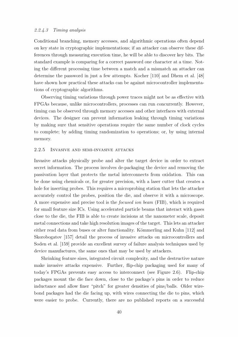
2.2.4.3 Timing analysis
Conditional branching, memory accesses, and algorithmic operations often depend
on key state in cryptographic implementations; if an attacker can observe these dif-
ferences through measuring execution time, he will be able to discover key bits. The
standard example is comparing for a correct password one character at a time. Not-
ing the different processing time between a match and a mismatch an attacker can
determine the password in just a few attempts. Kocher [110] and Dhem et al. [48]
have shown how practical these attacks can be against microcontroller implementa-
tions of cryptographic algorithms.
Observing timing variations through power traces might not be as effective with
FPGAs because, unlike microcontrollers, processes can run concurrently. However,
timing can be observed through memory accesses and other interfaces with external
devices. The designer can prevent information leaking through timing variations
by making sure that sensitive operations require the same number of clock cycles
to complete; by adding timing randomization to operations; or, by using internal
memory.
2.2.5 Invasive and semi-invasive attacks
Invasive attacks physically probe and alter the target device in order to extract
secret information. The process involves de-packaging the device and removing the
passivation layer that protects the metal interconnects from oxidation. This can
be done using chemicals or, for greater precision, with a laser cutter that creates a
hole for inserting probes. This requires a microprobing station that lets the attacker
accurately control the probes, position the die, and observe it with a microscope.
A more expensive and precise tool is the focused ion beam (FIB), which is required
for small feature size ICs. Using accelerated particle beams that interact with gases
close to the die, the FIB is able to create incisions at the nanometer scale, deposit
metal connections and take high resolution images of the target. This lets an attacker
either read data from buses or alter functionality. Kommerling and Kuhn [112] and
Skorobogatov [157] detail the process of invasive attacks on microcontrollers and
Soden et al. [159] provide an excellent survey of failure analysis techniques used by
device manufactures, the same ones that may be used by attackers.
Shrinking feature sizes, integrated circuit complexity, and the destructive nature
make invasive attacks expensive. Further, flip-chip packaging used for many of
today’s FPGAs prevents easy access to interconnect (see Figure 2.6). Flip-chip
packages mount the die face down, close to the package’s pins in order to reduce
inductance and allow finer “pitch” for greater densities of pins/balls. Older wire-
bond packages had the die facing up, with wires connecting the die to pins, which
were easier to probe. Currently, there are no published reports on a successful
40

fl ip-chipwire bond
Figure 2.6: A wire-bond package is shown on the left where the die faces up with wiresbonded connecting it to the solder balls through a substrate; in the flip-chip package onthe right the down-facing die has “bumps” used to connect it to the circuit board substrateusing solder balls.
invasive attack against a volatile FPGA.
Semi-invasive attacks require the removal of the device’s packaging, leaving the
passivation layer intact, while the rest of the analysis is done using techniques such
as imaging and thermal analysis. This class of attacks were introduced by Skorobo-
gatov [157] and covers the gap between the non-invasive and invasive types. Semi-
invasive attacks are cheaper than invasive ones since they typically do not require
expensive equipment or extensive knowledge of the chip; Skorobogatov has applied
these attacks on devices fabricated with 250 nm and larger manufacturing technolo-
gies. As with invasive attacks, I am not aware of successful applications of these
techniques on recent FPGAs.
2.2.5.1 Data remanence
Exploiting data remanence can be considered a semi-invasive technique, where the
attacker relies on the retention (or evidence) of previously stored state in storage
media or RAM cells after power loss, and even after data has been overwritten. Ionic
contamination, hot-carrier effects, and electromigration, for example, can “impress”
the stored state over time. Gutmann [79, 80] covers remanence of magnetic media
and RAM at length. High voltages or low temperatures can cause RAM to retain the
previous state from microseconds to minutes after power is removed depending on
the extremities of the conditions. In 2002, Skorobogatov [156] tested eight SRAM
devices (manufactured at 250 nm technology and larger feature-size), all showing
remanence of up to a few seconds at sufficiently low temperatures. In 2008, Hal-
derman et al. [82] demonstrated similar remanence in DRAM, where despite the
requirement for refreshing, memory modules retained state for up to an hour when
cooled to −196 with liquid nitrogen. They were able to extract software disk en-
cryption keys stored in DRAM this way, violating the implicit, and false, assumption
that data is erased instantly with power loss.
The work most relevant to FPGAs is Tuan et al. [174] who measured the re-
manence of 90 nm FPGA memory cells. The authors point out that previous data
taken for SRAM devices do not apply to FPGA SRAM cells. Firstly, because they
stem from older technologies with less leakage current, which affects charge and dis-
41

charge characteristics. And secondly, because FPGA SRAM cells are built, laid out
and arranged differently than commodity SRAM chips; even within the same device
there are several types of SRAM cells that are powered differently. The experiment
was done by continuously reading back the FPGA content and recording the change
in state of every SRAM cell at −40 , 0 and 25 for both floating or grounded
power rails. The authors found an asymmetry in remanence rates between cells
that are initially set to 1 (shorter) and those set to 0 (longer) due to the asymmet-
ric arrangement of the five-transistor cell. Cells were classified into two categories,
logic and interconnect; the state of logic cells (i.e., ‘1’ or ‘0’) are evenly distributed,
whereas only about 10–20% of interconnect cells are set to 1 for any design. The two
types of cells are also powered by different internal supplies. The results show that
interconnect cells retain state longer than logic cells: 40 seconds for interconnect
and 1 second for logic at −40 (worst case) for 20% of data to be lost when power
rails are left floating. However, if power rails are grounded, 20% of data is gone in
under 1 ms. One way to limit the window of remanence is to sense the die’s temper-
ature and shut down if it falls below a given threshold. This can be done internally
(for example, by using the Virtex-5 “system monitor” [186, UG192]) or externally
with an appropriate sensor inside a tamper resistant enclosure. Additionally, as a
response to tampering, on every power down, or on reconfiguration, SRAM power
rails should be actively grounded briefly rather than left floating.
2.2.6 Others
In cryptography, brute force search means attempting all possible key values to
search for a valid output. It can also mean exhaustion of all possible logic inputs to
a device in order, for example, to make a finite state machine reach an undefined state
or discover the combination to enter the device’s “test mode”. Another form of brute
force attack is the gradual variation of the voltage input and other environmental
conditions, rather than variation of logic states. Brute force is sometimes associated
with black-box attacks that attempt to exhaust all input combinations and record
the outputs in order to reverse engineer the device’s complete operation, or create
a new design that mimics it. Considering the stored state, complexity, and size
of current FPGAs, this type of attack is not likely to be practical or economic for
reverse engineering the FPGA’s entire functionality [185]. That said, if a subset of
the functionality is targeted that can be interfaced with directly through the I/O
pins, brute forcing can be fruitful, perhaps in combination with other attacks. For
critical functions, therefore, randomization may be useful. Christiansen [36] suggests
adding “decoy circuits” to the design to increase the effort of an attacker. The cost
is high, though: seven times LUT usage and twice the amount of power, in addition
to requiring more I/Os and design time.
42
Crippling attacks either subvert a system to perform malicious functions or com-
pletely bring it offline, similar to denial-of-service attacks on networked servers and
devices. The absence of robust integrity preserving mechanisms for bitstreams, such
as authentication, enables anyone to program an FPGA if they have access to it.
In the case where bitstream encryption is used (see Section 2.3.1) confidentiality is
provided, but may not be sufficient, as an adversary can still re-program the device
with an invalid bitstream and bring the system off-line. An extreme crippling sce-
nario is described by Hadzic et al. [81] where an FPGA is permanently damaged due
to induced contention by using invalid bitstreams, and we will discuss this further
in Section 2.3.2 on configuration authenticity.
Fault injection or glitch attacks can cause devices to perform operations in unin-
tended order or get them into a compromised state such that secret data is leaked.
This is done by altering the input clock, creating momentary over- or under-shoots
to the supplied voltage, electrical fields applied with probing needles, light flashes
applied to depackaged ICs, etc. As an example, if a conditional branch is skipped
by the CPU due to a clock glitch some commands will not be executed; a voltage
surge or trough can cause registers to keep their state. If a power glitch is applied
at the right time, the number of rounds of an encryption algorithm may be reduced;
Anderson and Kuhn [13] demonstrate how glitches and fault injections were used to
attack microcontrollers.
Ionizing radiation can also cause configuration memory cells to change state, and
thus change circuit behavior. If the affected circuit is part of a security function, then
protection mechanisms can be disabled, provided that radiation can be accurately
(and consistently) focused on particular areas of the IC. FPGAs have been tested
while exposed to ambient radiation and accelerated particle beams for measuring
their susceptibility to single event upsets (SEUs)11, which may affect configuration
behavior [92, 125]. Maingot et al. [128] have also exposed FPGAs to laser shots and
analyzed the fault patterns. Some volatile FPGAs now have an internal function that
detects SEUs in the background as the design operated in user logic [7, AN357] [186,
AN714]. This is done by periodically comparing a calculated CRC or Hamming
syndrome to a pre-computed one, alerting the user logic on discrepancy (so the
developer can decide what action to take). Triple modular redundancy (TMR) is
another solution, where all logic is triplicated and majority voters detect radiation-
induced logic faults; TMR is primarily used in space applications where radiation
faults are more frequent. Many applications that use TMR also periodically “scrub”
FPGA configuration and data to restore it to a known state to recover from SEUs
that may have occurred. These technique could be adopted to protect against
11“Radiation-induced errors in microelectronic circuits caused when charged particles lose energy byionizing the medium through which they pass, leaving behind a wake of electron-hole pairs” [137].
43

malicious radiation attacks. Finally, for protecting cryptographic implementations
against fault attacks and side channel analysis, Mentens et al. [135] propose to use
partial dynamic reconfiguration to randomly change the physical location of design
modules.
2.3 Defenses
2.3.1 Configuration confidentiality
The idea of encrypting configuration content for programmable devices was first
suggested in a 1992 patent by Austin [18]. Actel’s 60RS device family was the first
to encrypt configurations, though the implementation is a good example of poor
key distribution. Actel programed the same key into all devices (preventing reverse
engineering, not cloning), and the same key was also stored in every instance of
the software, so attackers only needed to reverse engineer the code, rather than use
invasive techniques [102]. In 2000, Xilinx added a hard-core Triple-DES bitstream
decryptor to their Virtex-II family, which allowed developers to store their own keys
in internally battery-backed RAM. Bitstream encryption is now a standard function
in high-end FPGAs, and works as follows.
After generating the plaintext bitstream, the user defines a key and the software
encrypts the configuration payload of the bitstream. The user then “programs” this
same key into dedicated memory in the FPGA. A command in the bitstream header
instructs the configuration logic to pass all configuration data through the hard-core
decryptor before the configuration memory cells are programmed. Some FPGAs
(such as Altera’s Stratix II/III) can be set to always perform decryption, regardless
of header commands, which prevents the loading of bitstreams not encrypted with
the correct key.
There are two on-chip key-storage techniques for bitstream decryption: volatile
and non-volatile. Using volatile storage, keys are kept in low-power SRAM cells,
powered by an external battery attached to a dedicated pin. The advantages of
volatile key storage are that it allows quick clearing the keys in response to tamper-
ing even when the device is not powered, and also complicating attacks by forcing
attackers to constantly power the device. Security-conscious designers find these
attributes appealing, as it makes conformance to standards, such as the U.S. gov-
ernment’s FIPS 140-2 [139], easier and in general provides higher levels of security
than non-volatile key storage. The battery requirement is generally seen as a disad-
vantage because it takes up PCB space (especially if a battery holder is required),
may have higher failure rate than other components, and may require replacement
in devices with a long shelf or use periods.
With non-volatile memory key storage, keys are permanently embedded in the
44

device using fuses, laser programming, Flash, or EEPROM. This type of key storage
combined with the latest CMOS technology is a recent development, as it introduces
a non-standard manufacturing step that impacts yield and reliability. Embedded
keys have the advantage of not requiring a battery and the cost of bitstream encryp-
tion is included in the FPGA’s price (if key management costs are ignored). For
these reasons, this approach appeals to cost-conscious designers over the battery
option. Embedded keys can also help prevent run-on-fraud as the keys can be pro-
grammed into the device at a trusted facility before being shipped to a third party
for system assembly and testing.
Key management is the process of key generation and distribution (transport)
for and to communicating parties, either prior to or after initiating contact. NIST’s
FIPS 800-57 [139], Recommendation for key management, remarks that “key man-
agement is often an afterthought in the cryptographic development process. As
a result, cryptographic subsystems too often fail to support the key management
functionality and protocols that are necessary to provide adequate security[. . . ] key
management planning should begin during the initial conceptual/development stages
of the cryptographic development life cycle”. As the security of the system should
rely on the secrecy of keys, their management infrastructure is as important as the
choice of cryptographic algorithm or protocol. The logistics of keeping keys se-
cret while stored, transported and updated, along with adequate access controls,
amounts to a non-trivial cost that must be incorporated into the overall cost of a
defense strategy; at the least, procedures for key management should be defined. It
is also quite possible that the total cost of a defense strategy could exceed the loss
due to theft. Unfortunately, we see very little discussion of key management in the
FPGA security literature when new security schemes are being proposed.
Up to now we have discussed existing solutions for encrypting configurations,
though other schemes have been proposed. Kean [102] suggested that embedded
keys (programmed by FPGA vendors, foundries, or system developers) be used such
that the FPGA itself can encrypt and decrypt the bitstream without the key ever
leaving the FPGA. As outlined in Figure 2.7, the first stage happens in a trusted
facility where the plaintext bitstream is encrypted by the FPGA using its embedded
key KCL, and then stored in NVM. While the system is deployed in the field, the
bitstream is decrypted with the same embedded key using a hard-core decryptor
that is part of the configuration logic.
Kean [102] also made the observation that it may be sufficient to only slightly
increase the price of cloning and suggested embedding fixed keys in the photo masks
(artwork) that are used in the FPGA manufacturing process: “Suppose there were
five possible keys and FPGA’s were supplied with no markings indicating which key
was in a particular FPGA. The design owner can use any FPGA since the FPGA
45
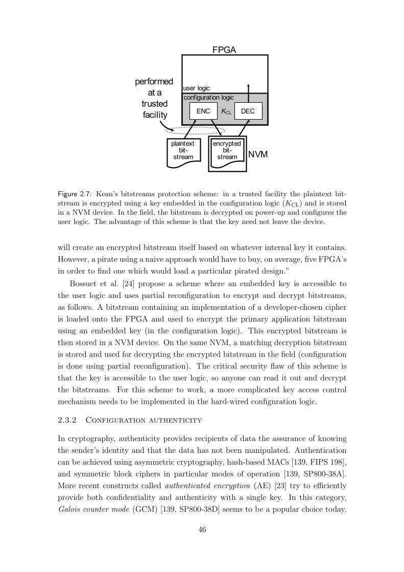
NVM
FPGA
user logicconfiguration logic
performed at a
trusted facility DECKCL
plaintextbit-
stream
encryptedbit-
stream
ENC
Figure 2.7: Kean’s bitstreams protection scheme: in a trusted facility the plaintext bit-stream is encrypted using a key embedded in the configuration logic (KCL) and is storedin a NVM device. In the field, the bitstream is decrypted on power-up and configures theuser logic. The advantage of this scheme is that the key need not leave the device.
will create an encrypted bitstream itself based on whatever internal key it contains.
However, a pirate using a naive approach would have to buy, on average, five FPGA’s
in order to find one which would load a particular pirated design.”
Bossuet et al. [24] propose a scheme where an embedded key is accessible to
the user logic and uses partial reconfiguration to encrypt and decrypt bitstreams,
as follows. A bitstream containing an implementation of a developer-chosen cipher
is loaded onto the FPGA and used to encrypt the primary application bitstream
using an embedded key (in the configuration logic). This encrypted bitstream is
then stored in a NVM device. On the same NVM, a matching decryption bitstream
is stored and used for decrypting the encrypted bitstream in the field (configuration
is done using partial reconfiguration). The critical security flaw of this scheme is
that the key is accessible to the user logic, so anyone can read it out and decrypt
the bitstreams. For this scheme to work, a more complicated key access control
mechanism needs to be implemented in the hard-wired configuration logic.
2.3.2 Configuration authenticity
In cryptography, authenticity provides recipients of data the assurance of knowing
the sender’s identity and that the data has not been manipulated. Authentication
can be achieved using asymmetric cryptography, hash-based MACs [139, FIPS 198],
and symmetric block ciphers in particular modes of operation [139, SP800-38A].
More recent constructs called authenticated encryption (AE) [23] try to efficiently
provide both confidentiality and authenticity with a single key. In this category,
Galois counter mode (GCM) [139, SP800-38D] seems to be a popular choice today.
46

Encrypting configuration files protects against cloning and reverse engineering in
transit independently of the FPGA, while authentication guarantees the correct and
intended operation of the bitstream while it is running on the FPGA. Parelkar [144,
145] suggested the use of authenticated encryption for protecting FPGA bitstreams
and concluded that the dual-pass Counter with CBC-MAC (CCM) mode [186,
SP800-38C] is the best choice. Later, Parelkar and Gaj [146] also described an
implementation of EAX [21], suggesting it be used for bitstream authentication.
But their discussions of bitstream authentication’s benefits were very brief, and the
constraints bounding a solution were not thoroughly investigated.
In early 2007 I provided the following analysis of the problem [50], and motivated
the addition of authentication to the hard-coded configuration logic of the FPGA.
My approach was to provide a convincing case such that FPGA vendors may be
persuaded that such addition is a worth-while investment for them.
I proposed that authentication can allow source code audit under some con-
straints (such as supply chain control). Many manufacturers do not make their
source code publicly available, so consumers have no way of knowing what their
devices’ firmware is actually doing. For some this may not be a problem, though
for some applications source code transparency is critical. Figure 2.8 shows a hypo-
thetical code audit process I proposed that is enabled using authentication (with-
out encryption) for a voting machine application. A municipal “voting authority”
ordered voting machines from “Honest Voting Machines” (HVM). Both sides are
interested in allowing the voting authority to examine the HDL code so that they
can be sure that the audited version is indeed the one operating on the FPGA at
voting time. However, HVM are adamant that only their authorized code is run
on their voting machines. HVM starts by programming a unique authentication
key into a dedicated key store inside of the FPGA. The source HDL is then sent
to the voting authority, and optionally also published online for voters to examine.
“In general, authentication is more important than encryption” con-clude Ferguson and Schneier [63, p116]. That is, impersonation can be moredevastating than just being able to eavesdrop on communications. This makessense for FPGA configurations as well: being able to configure an FPGA with amalicious bitstream can be more harmful than just being able to reverse engineerit. Consider an FPGA-based banking hardware security module (HSM) wherebitstreams can be remotely updated. An attacker learning how the moduleworks by reverse engineering the bitstream may be able to create a competingproduct or even find exploitable vulnerabilities. On the other hand, if the at-tacker can also configure the HSM’s FPGA with a modified bitstream, he couldclandestinely control and observe all traffic (i.e., credit card PINs, personal de-tails, etc.)
47

systemdeveloper
votingauthority
HDLsource
SW flow
FPGA
user logic
MACKCL
configuration logic
user logic
MACKCL
configuration logic
MACKCL
HDLsource
bit-stream
SW flow
bit-stream
MAC
FPGA
software settings
audit
Figure 2.8: HDL source code audit scheme [50]. Bitstream authentication can enable codeaudit by having the end user compile the HDL code he audited himself. This way, theHDL can be public but only run if the correct MAC is supplied by the manufacturer.
HVM compiles the HDL into a bitstream, generates its MAC using the FPGA’s
authentication key, and delivers the MAC to the voting authority.
The voting authority then audits the code to see that there are no biases, back-
doors, or other behaviors that may alter election results; it is prevented from modi-
fying the code because it will produce a different bitstream without a corresponding
MAC. Once satisfied, the voting authority compiles the code into a bitstream iden-
tical to the one used by HVM to compute the MAC. In order for the exact bitstream
to be produced at both sides, the same software version and settings (i.e., cost tables,
optimization efforts, etc.) must be used. Since the bitstream was compiled locally,
the voting authority is assured that the audited HDL resulted in the bitstream it
programs into the FPGA before the elections. Finally, the FPGA must only accept
encrypted bitstreams.
Bitstream authentication also solves bit manipulation of encrypted bitstreams,
as is possible with CBC and counter modes of operation, for example. Relying on
linear error correction and detection codes, such as cyclic redundancy (CRC), for
integrity is not satisfactory because they can be forged such that manipulation is not
detected [166]. (Currently, CRC is used to prevent bitstreams that were accidentally
corrupted in transmission from being activated so short circuits do not occur.)
Hadzic et al. [81] examined the implications of malicious tampering of bitstreams.
Currents from circuit shorts may cause the device to exceed its thermal tolerance,
permanently damaging it. A random-content bitstream may potentially create con-
48

AES(confiden-
tiality)
AES(authenti-
city)
MACresult
bitstream'sMAC
compare
key_auth
key_dec
start or restart
configurationmemory cells
FPGA configuration logic
ambit-
stream
Figure 2.9: Bitstream authentication scheme [50]. The bitstream is decrypted and authen-ticated in parallel. The bitstream’s appended and computed MACs are compared; if theymatch the start-up sequence executes, otherwise, the configuration memory cells are reset.
siderable contention and is relatively simple to construct (if it is made to be accepted
by the FPGA). Hadzic et al. have proposed several system-level solutions to protect
against the issues they raise, but have not considered authentication, which can
solve all of them.
I propose a generic composition scheme for decryption and authentication of bit-
streams, shown in Figure 2.9 [50]. I eliminated asymmetric cryptography for their
relative high cost in circuit size (for the required throughput), and also authenti-
cated encryption because a good solution would enable the encryption and authen-
tication to be separate (so to enable code audit and key distribution versatility, for
example)12. In Chapter 4, I will present an AES implementation architecture for
processing concurrent bitstreams in different modes, as suggested above. Although
it is not an ASIC implementation, as would be required for integration into the
configuration logic of FPGAs, it does demonstrate the novel use of resources for
multi-stream processing. In Chapter 3, bitstream authentication is considered for
enhancing the security properties of remote configuration updates.
2.3.3 Design theft deterrents
FPGA vendors offer a few cloning deterrents that rely on the bitstream encoding
secrecy to obfuscate secrets. Indeed, they are not cryptographically secure but may
increase the cost of cloning to a level sufficient to some cost-conscious designers, and
intended mostly for low-end devices that do not decrypt bitstreams.
12One of my criteria was that a mode is “approved” by some authority in order for it to be adopt-able by FPGA vendors. Since the paper’s publication, GCM and GMAC [139, SP800-38D] werepublished by NIST, and meet this and other criteria.
49

NVM
FPGA
user logic
configuration logic
RNG
plaintextbit-
stream
KUL
MAC
KUL
MACchallenge
responsecomp-are
processorwith NVMfunction
Figure 2.10: A challenge-response cloning deterrent scheme where a shared key KUL isstored in an external processor, and also obfuscated in the bitstream. When this bitstreamis loaded onto the FPGA, a random challenge is produced internally and is sent to theprocessor, which responds with a MAC of this challenge. An enable signal is asserted ifthe internal computation and received response match.
In 2000, Kessner [106] proposed an FPGA bitstream theft deterrent using a
“cryptographically secure variation on a Linear Feedback Shift Register (LFSR)”
(i.e., stream cipher): a user logic application computes a bit-string and compares
its output to a string sent by a complex programmable logic device (CPLD) that
performed the same operation. This lets the application inside of the FPGA “know”
that it is mounted on the “right” circuit board. More recently, Altera [7, WP
M2DSGN] and Xilinx [186, AN780] proposed very similar challenge-response cloning
deterrents, shown in Figure 2.10. The user logic application shares a key KUL with
a processor that is placed beside it on the printed circuit board. The FPGA sends a
challenge produced by a true random number generator to the processor and both
MAC it (using cipher-based MAC, HMAC, etc.) The processor sends the result back
to the FPGA for comparison; if the results match, the application is enabled. For
secure implementation, developers need to be careful such that the random number
generator is not easily influenced by temperature and voltage variations, as well
as consider the potential compromise from readback difference, replay and relay
attacks, as we will discuss in Chapter 6.
In the Spartan-3A device family, Xilinx offers “Device DNA”, a non-volatile,
factory-set, user-logic accessible, 55-bit unique number [186, UG332, p241]. Xilinx
suggests using this number as a “key” for deterrents that use an external device in
similar, or less secure, ways than the ones described above. Since the serial number
is no secret – it can be read by anyone who configures the FPGA – Xilinx proposes
that the attacker’s challenge would be to discover the algorithm used for processing
this number [186, WP266], which goes against Kerckhoffs’ principles [105].
These schemes rely on the continued secrecy of bitstream encoding for secur-
ity, which can provide an incremental challenge to would-be attackers when active
50
measures are not available. We discussed the issues of bitstream reversal in Sec-
tion 2.2.1; unfortunately, we cannot quantify how much protection such schemes
actually provide, and how long this type of protection can last.
2.3.4 Watermarking and fingerprinting
A digital watermark, placed into digital content by its owner, is a hard-to-remove
evidence of ownership that is unnoticeable to an observer; it ties the content to its
creator, owner, or the tool that produced it. A fingerprint is a watermark that is
varied for individual copies, and can be used for identifying individual authorized
users of the content. For example, watermarks can be encoded as human-inaudible
frequencies in audio files, or in the least significant bits of images that affect content
below the sensitivity threshold of human vision. The original content, therefore, is
altered but in ways that are unnoticeable to the user. Ideally, watermarks should be
easy to insert using the software development flow; not affect correct functionality;
use as little resources possible; be unforgeable and hard to remove; and be sufficiently
robust so they can be used as evidence of theft. Kahng et al. [100] provide the
fundamentals of watermarking techniques for integrated circuits and FPGA design
marking; Abdel-Hamid et al. [1] provide a good survey and analysis of watermarking
techniques in general.
Watermarks can be inserted at three stages of the FPGA design flow: HDL,
netlist, or bitstream. HDL watermarks can work for system developers marking
their own designs, but not for externally integrated cores because those marks can
be easily removed. Watermarks in encrypted netlists may work for protecting such
external cores, though the software needs to support an encrypted development flow
in a way that cannot be circumvented. In both HDL- or netlist-level watermarks,
the tool chain must allow the watermark to be preserved throughout the process
of generating a bitstream. Bitstream-level insertion can only be performed by the
system developer; otherwise, bitstreams would require post-processing by the cores
vendor who had no control over the design flow. This is logistically cumbersome,
but may also be impossible without the ability to reverse engineer portion of the
bitstream.
Lach et al. [118] address FPGA bitstream watermarking and fingerprinting for
design protection, suggesting embedding content or functions into unused LUTs
(“additive-based” marking). To avoid an “elimination attack” by colluding recipi-
ents of the same design with differing marks, the authors suggest varying placement
for every bitstream instance. A possible attack against this scheme is to remove
LUT content from unencrypted bitstreams while checking that the design still works
correctly, iteratively removing identifying marks; “masking attacks” are also possi-
ble by inserting random content into all LUTs that are not used. Lach et al. [119]
51

later improved the technique by splitting the watermark into smaller pieces such
that masking attacks are harder. Building on the constraint-based ideas of Kahng
et al. [100], Jain et al. [95] propose placing-and-routing a portion of a completed de-
sign to incorporate design-specific timing constraints as watermarks. This produces
a unique bitstream that can be regenerated given the original HDL and constraints
in order to show ownership. This may work for a complete design rather than the
more desirable marking of individual cores, because a core vendor cannot enforce
constraints through a netlist such that they always produce the same bitstream por-
tion when multiple cores are combined together by the system developer. Le and
Desmedt [121] describe possible attacks on the schemes of Kahng et al. [100] and
Lach et al. [118, 119]; however, the ones relating to LUT-based marks will require
reverse engineering the bitstream, at least partially, so are not as straightforward as
it first seems.
Ziener et al. [191] propose using the LUT content extracted from netlists as a
watermark. Then, LUT content is extracted from a suspected copied bitstream to
statistically determine if an unlicensed core is present; since the LUTs are part of
the functional design, removing them may make the design not work, so it resists
elimination and masking attacks. Ziener and Teich [190] propose using LUT-based
signatures that can be measured through power analysis after an external trigger.
Watermarks are a reactive mechanism and as such do not actually prevent theft,
but may serve as initial evidence in court or trigger further investigation. However,
while it would make a hard case for a criminal to claim that he independently
arrived at an identical copy of artwork such as a photographs or song, it is quite
possible that engineers independently produce very similar code, ones that may
falsely trigger the statistical threshold for fraud in watermarking schemes. (This is
especially true since synthesis tools interpret different HDL descriptions to produce
similar netlists.) Thus, watermarking schemes must be robust enough such that the
probability of this happening is very low. On top of that, reactive mechanisms are
only useful where ownership rights are enforced, further reducing their usefulness.
As counterfeit hardware tends to come from countries where this is not the case,
these mechanisms are less appealing compared to active ones.
Lastly, some watermarking techniques rely on the continued secrecy of bitstream
encoding, opening them to various manipulation attacks that may prevent them
from being used as conclusive evidence in court (more in box on the next page). If
the attacker encrypts the original plaintext watermarked bitstream, the detection
and proof is made more difficult, if possible at all. For all the reasons above, water-
marking may only be useful when it can be conveniently applied and verified, but as
part of an overall active defense mechanism. This will serve as a deterrent and help
protect the watermark from tampering, but also provide evidence that the infringer
52

had to actively attack the system in order to remove it.
2.3.5 Physical unclonable functions
Physical unclonable functions (PUFs) extract unique strings from the physical prop-
erties of objects. Pappu [142] and Pappu et al. [143] introduced physical one-way
functions where the scatter pattern from a laser beam passing through, or reflected
from, a block of epoxy is converted into a bit string unique to that block. Buchanan
et al. [28] use the microscopic arrangement of paper fiber as an identifier, which
turns out to be very reliable, even after moderate physical abuse. Since the PUF’s
output is physically coupled to the item, and is supposed to be unique, it may be
suitable for authentication.
Silicon PUFs (SPUF) were introduced by Gassend et al. [69], Lee et al. [122], and
Lim et al. [126], and rely on uncontrollable variability of integrated circuit manufac-
turing. An “arbiter PUF” is shown in Figure 2.11, where identically designed delay
lines are routed through multiplexers that are controlled by a challenge vector. A sig-
nal edge is split to propagate both routes according to the multiplexers’ setting until
it reaches the sampling register. The response is determined by which signal arrives
first. All possible paths are designed and laid out to have the same propagation
delay, but because integrated circuit fabrication introduces minute uncontrollable
path variations, each instance of the entire structure can be different, so giving a
different result. If m of the structures shown in Figure 2.11 are replicated, challenge
Watermarking in the real world. Anderson [10, ch22.4] puts the legal valueof watermarking in the context of the real world. He observes that intellectualproperty lawyers “almost never” have a problem proving ownership using stan-dard documents and contracts, and that they do not need to resort to technicalmeans, which end up confusing the jury anyway. Another observation is thatkey management should be done with care if keys are to be disclosed in court,so they do not compromise many other marks.On a related note for the last point, in June 2009 a U.K. judge ruled in favorof Halifax Bank after one of its customers sued them for money he lost to“phantom withdrawals”a. The bank could have provided a cryptographic keyto prove that its customer was at fault, but instead claimed that they cannotderive the key again, and that disclosing it in court may compromise othersystems (both claims seem to be technically incorrect, by the way). The casewas won by the bank providing an undocumented log sheetb pointing to a fewdigits that implicate the cardholder without being required to produce moreconcrete evidence, such as a cryptographic key.
a“Chip and PIN on Trial”,http://www.lightbluetouchpaper.org/2009/04/09/chip-and-pin-on-trial/bhttp://www.cl.cam.ac.uk/~rja14/Papers/halifax-log.pdf
53

challenge[n:0]
0
1
0
1
0
1
0
1
0
1
0
1
0
1
0
1
D Q
edge
response
samplingregister
Figure 2.11: “Arbiter PUF” [126]. A signal’s rising edge is split to propagate throughmultiplexers controlled by a challenge vector. The result depends on which of the two edgesarrives first. The routes are designed to be identical, though uncontrollable manufacturingvariability causes them to have minute variations in length.
vectors of size n controlling the multiplexers, provide 2n challenges-response pairs of
size m. Results from an implementation of a delay-based PUF variation are reported
by Majzoobi et al. [129].
Suh and Devadas [167] also suggested the “ring oscillator PUF” where many
identical free-running ring oscillators are used to produce unique bitstrings based
on slight delay variations between the oscillators’ inverters. Tuyls et al. [175] have
developed a “coating PUF” which is applied to the surface of a die such that the
coating’s unique dielectric distribution can be measured capacitively from within
the device to extract a key and detect invasive tampering. Guajardo et al. [75] and
Holcomb et al. [88] propose using the initial state of SRAM cells as a source of en-
tropy. This works because manufacturing variability and environmental conditions
cause SRAM cells to initialize to one of the two state on power-up if they are not
actively driven to any particular one. Guajardo et al. reported that large SRAM
blocks within some FPGAs13 can be used for establishing unique keys that may be
used for design protection. Holcomb et al. similarly showed that SRAM device be-
havior can be used for RFID token authentication or for random number generation.
(Note that the goals of PUFs and TRNGs are different: the former needs to produce
consistent results, while the latter is required to be a source of high entropy.)
Ideal PUFs – that is, ones that function as pseudorandom number generators
seeded from strings derived from the physical properties of a circuit – can be very
attractive for the following reasons: creating a model for faking them is hard; derived
keys “exist” on demand; invasive tampering may permanently alter PUF output;
cryptographic keys do not need to be programmed into, or ever leave, the device;
13Oddly, the authors do not specify which FPGA they used, and make rather general claims abouttheir solution’s applicability to all FPGAs. Since current Xilinx FPGAs initialize BRAM statein the bitstream, it is likely that they have used the large M-RAM blocks inside of some AlteraFPGAs (only available in Stratix or Stratix II), which are not initialized on configuration [7, StratixII Handbook, Volume 2, p32].
54
they are scalable; and finally, they may work with existing FPGAs.
2.3.5.1 Secure processor-code distribution
Some FPGA families incorporate hard-coded embedded sequential processors, while
many others support “soft” processors, such as the Altera Nios and Xilinx MicroB-
laze, which are implemented in user logic. The code for these processors can be
written in a high-level language such as C, with the compiled code stored in embed-
ded RAM such that it can be updated without full reconfiguration. Simpson and
Schaumont [155] suggest using PUFs for installing and updating proprietary com-
piled code14 that does not belong to the system developer. Their proposed protocol
authenticates and decrypts code based on keys derived from challenge-response pairs
collected from an embedded PUF, as described in Section 2.3.5. For each FPGA,
the FPGA vendor records a large number of challenge-response pairs from the “PUF
extractor” design running on the FPGA and enrolls those, and the FPGA’s unique
identifier, with a trusted party. Then, cores vendors enroll their compiled code,
together with a unique identifier, with the trusted party. Through several crypto-
graphic exchanges between the principals, the compiled code is encrypted such that
it can only be decrypted and used by FPGAs that can reproduce the correct PUF
response given a particular challenge vector. The scope to which this scheme applies
is limited to the secure distribution of compiled code for embedded processors and
does not apply to cores that use the FPGA’s other user logic resources. Guajardo
et al. [75] suggest enhancements to this protocol (but does not increase its scope)
and also describe an implemented PUF, as discussed in the previous section, which
was originally only simulated by Simpson and Schaumont.
2.3.5.2 PUFs and the FPGA usage model
In order to be practically used as part of a cryptographic application, PUF instan-
tiations must harness sufficient entropy and produce responses consistently across
temperature and voltage variations. In addition, the probability of more than a
single device producing the same response to a given challenge should be demon-
stratively low enough such that a search for matching devices is impractical. Despite
not being able to verify any of the results reported in the literature so far (see more
on reproducibility in Chapter 5), let us now assume that they can be made to work
reliably on FPGAs and consider how they can be used in practice.
The “PUF extractor” circuit needs to be loaded onto the FPGA through the
ordinary configuration interface. If this initial bitstream is not encrypted, security
mechanisms can be circumvented (as we discussed in Section 2.2.1). I call this the
14Simpson and Schaumont [155] and Guajardo et al. [75] use the terms “software” and “IP” inter-changeably, which can be confusing and misleading; I use “compiled (C) code” for clarity.
55

“initial configuration problem” – if the initial bitstream is not trusted (i.e., can
be reverse engineered, manipulated, downgraded, etc.), then nothing can be truly
trusted beyond that point. As a solution, we may be tempted to suggest that PUF
extractor bitstreams be encrypted and authenticated (as discussed in Sections 2.3.1
and 2.3.2). But if they are, we may realize that if a remote server already knows
the appropriate keys, then PUFs provide little additional value, especially given the
high logistical and resource overhead (i.e., online cryptographic exchanges and logic
resources for the extractor).
An example for a rather contrived FPGA PUF application is Majzoobi et al. [129,
p20]. An FPGA is used as an authentication token, similar to a smartcard, so when
the “owner” sends a correct PIN to a remote server, the server remotely programs
the FPGA with a PUF extractor bitstream, and uses prerecorded challenge-response
pairs to authenticate the FPGA. When the session is done, somehow, the remote
server is able to force the FPGA to erase itself. This simple mechanism is vulnerable
to a range of attacks (some of which are identified by the authors): replay, readback,
man-in-the-middle, reverse engineering, denial-of-service, etc. One solution the au-
thors propose is to encrypt the bitstream. However, if the server already knows the
encryption key embedded in the configuration logic, there are many other ways to
perform an authentication session without a PUF (one is detailed in Chapter 3).
Another example is Guajardo et al. [75] who describe an FPGA “IP protection”
scheme using PUFs, but only dedicate a single sentence to the procedure of how the
FPGA may be configured remotely, and the implications of the FPGA usage model;
this description is too short to be meaningful.
I am aware of two companies that commercially develop PUF-based products,
Verayo and Intrinsic ID15, which spun out of MIT and Philips, respectively. Their
focus seems to be on PUFs for ASICs and RFID devices (as indicated on their web-
sites, April 2009). Both also briefly mention that their technology can be used with
FPGAs (“soft PUF”) for IP protection, but do not provide any further information.
To conclude, I have yet to come across a description of a PUF usage model for design
protection that provides a satisfying security analysis, or make a convincing case to
justify the overheads over other solutions. There may be better ways for achieving
similar design protection goals more practically and reliably.
2.3.6 Evolvable hardware
Modeled after biological evolution, mutated circuits are evaluated based on their
“fitness” scores in an iterative process to achieve desired functionality. Fitness of
a circuit, or portions of it, indicate the degree to which it meets the specifications.
Obviously, reconfigurable devices are a convenient platform for implementing such
15http://www.verayo.com/ and http://www.intrinsic-id.com/
56
circuits and they are used in this field quite extensively [73, 152, 153, 168].
The appeal of evolved circuits is that they significantly differ from conventional
ones, and can quickly adapt to new and unexpected conditions. Thompson and
Layzell [169] described “the most bizarre, mysterious” evolved circuit implemented
on a Xilinx XC6216 FPGA. The circuit was meant to distinguish between 1 kHz or
10 kHz input clocks without having a clock of its own. It worked, but remarkably,
the exact way in which the circuit achieved this functionality could not be fully
explained. The research suggests that the correct functionality is specific to the
physical attributes of the individual FPGA it ran on – the same circuit (i.e, bit-
stream) did not function correctly on other FPGAs of the same size and family. If
this can be reliably replicated, it means that we may be able to use evolvable circuits
to derive bitstrings that are unique to individual devices, similarly to PUFs. In a
patent, Donlin and Trimberger [49] suggest doing just that for bitstream protection.
Security based on evolvable circuits may suffer from similar issues discussed
above for PUFs, and be also problematic in the context of reproducible research as
discussed in Chapter 5.
2.3.7 Isolation
Some applications require that functions implemented on the same device be physi-
cally isolated such that sensitive data does not leak between them. This is sometimes
known as “red-black separation” where plaintext (red) is separated from ciphertext
(black) in the same system. Huffmire et al. [90] propose “moats” to isolate cores
and “drawbridges” macros to connect them so individual cores within a multi-core
FPGA design are adequately isolated. The cores are separated by unrouted columns
and rows, and may only communicate through pre-defined connections defined as
a macro. The authors describe a set of tools for bitstream-level verification of the
separation after the moats have been inserted in an ordinary design flow. The moats
are created by prohibiting PAR from placing logic or routes in specified rows and
columns that surround the functional block (the granularity of moats is a CLB).
Each CLB has a routing box that can route to 1, 2, 8 or 16 CLBs away with some
routings that span the whole chip, so depending on the moat’s width, certain route
lengths must also be prohibited from use such that the moats are not “bridged” by
the tools.
Similarly, and likely preceding the research of Huffmire et al., McLean and
Moore [131] reported a collaboration between Xilinx and the U.S. National Sec-
urity Agency (NSA) that yielded a set of tools and macros for isolation in the
Virtex-4 family of FPGAs. The analysis showed that a single CLB column “fence”
is sufficient to provide adequate isolation; connections between isolated functions
was done with pre-defined “bus macros”. Interestingly, the NSA-Xilinx report re-
57

veals that the Virtex-4 FPGA has gone though NSA analysis and was deemed secure
for red-black applications. Additionally, it discusses an internal “security monitor”,
but does not go into implementation details. A Xilinx patent also describes active
(i.e., real-time detection) circuits that monitor separation policy violation between
isolated cores [57].
Brouchier et al. [26] propose a method for bridging the CLB separation by using
a covert channel they call “thermocommunication”. The communication is done
through temperature modulation using ring oscillators, one for transmitting and
another for receiving data. The transmitter needs to be covertly inserted into a
high-security module (“red”) such that a receiver in a low-security module (“black”)
can demodulate, thus violating the multi-level security policy. The authors demon-
strated this to work on a Xilinx Spartan-3 for 1 bit/s throughput. The receiver
requires 200 slices, which is probably big enough to be detected by close inspec-
tion, though given that this is the low-security module, perhaps that is unlikely.
The transmitter’s size is not specified, though it is potentially smaller. The only
problems that remain are operational: how does one insert a Trojan circuit into an
NSA module without being detected, how and when are the circuits activated, and
how is the leaked data transmitted out? (Anderson et al. [9, p8] call these problems
“location, preparation, trigger, and control”.)
2.4 Conclusion
Since the late 1990s we have seen volatile FPGAs advance from simple logic de-
vices to large, complex, “systems on a chip”; designing with these devices requires
specialization and substantial investment. This chapter has aimed to capture the
current state for the “FPGA security” field and provide the foundations for future
discussions and for following chapters. In 2001, Kean [102] summarized: “Lack of
design security has long been the skeleton lurking in the closet of the SRAM FPGA
industry.” As we have seen, there are still many open problems and items to explore
for enhancing the security of FPGAs and designs made for them.
58

Chapter 3
Secure remote reconfiguration
Networked FPGA-based systems gain functional flexibility if remote configuration
updates are possible. Despite FPGAs having had the potential for “field repro-
grammability” since they became available, methods for performing secure field up-
dates over public networks have not been explored. The question of how to secure
updates against malicious interference may seem easily answered at first glance:
many existing cryptographic authentication protocols protect the confidentiality,
integrity and authenticity of transactions, such as overwriting a file in a remote
computer. Those can be easily applied if the FPGA is merely a peripheral device
in a larger system and the remote update of its configuration bitstream is handled
entirely by software running on the system’s main processor. In this work, however,
we consider the cases where a separate main processor is not present or is untrust-
worthy, and where only the FPGA and the applications it is running are responsible
for securing updates.
Two properties of volatile FPGAs are problematic under these conditions: they
lack sufficient memory for storing more than a single configuration at one time, and
they retain no configuration state between power-cycles. These properties, in turn,
have two main implications. Firstly, FPGAs have no notion of the “freshness” of
received configuration data, so they have no mechanism for rejecting revoked config-
uration content. Secondly, unless a trusted path is established with devices around
the FPGA (such as non-volatile memory), they have no temporary memory to store
the bitstream while it is being authenticated or decrypted before being loaded into
configuration memory. In other words, merely initiating a reconfiguration will de-
stroy the current state.
The primary observation we make is that the FPGA user logic can be used to per-
form security operations on the bitstream before it is stored in external non-volatile
memory (NVM) and loaded into the FPGA’s configuration memory cells. We then
rely on system-level properties, such as tamper proofing and remote attestation, to
compensate for the lack of cryptographic capabilities and non-volatile memory in
59
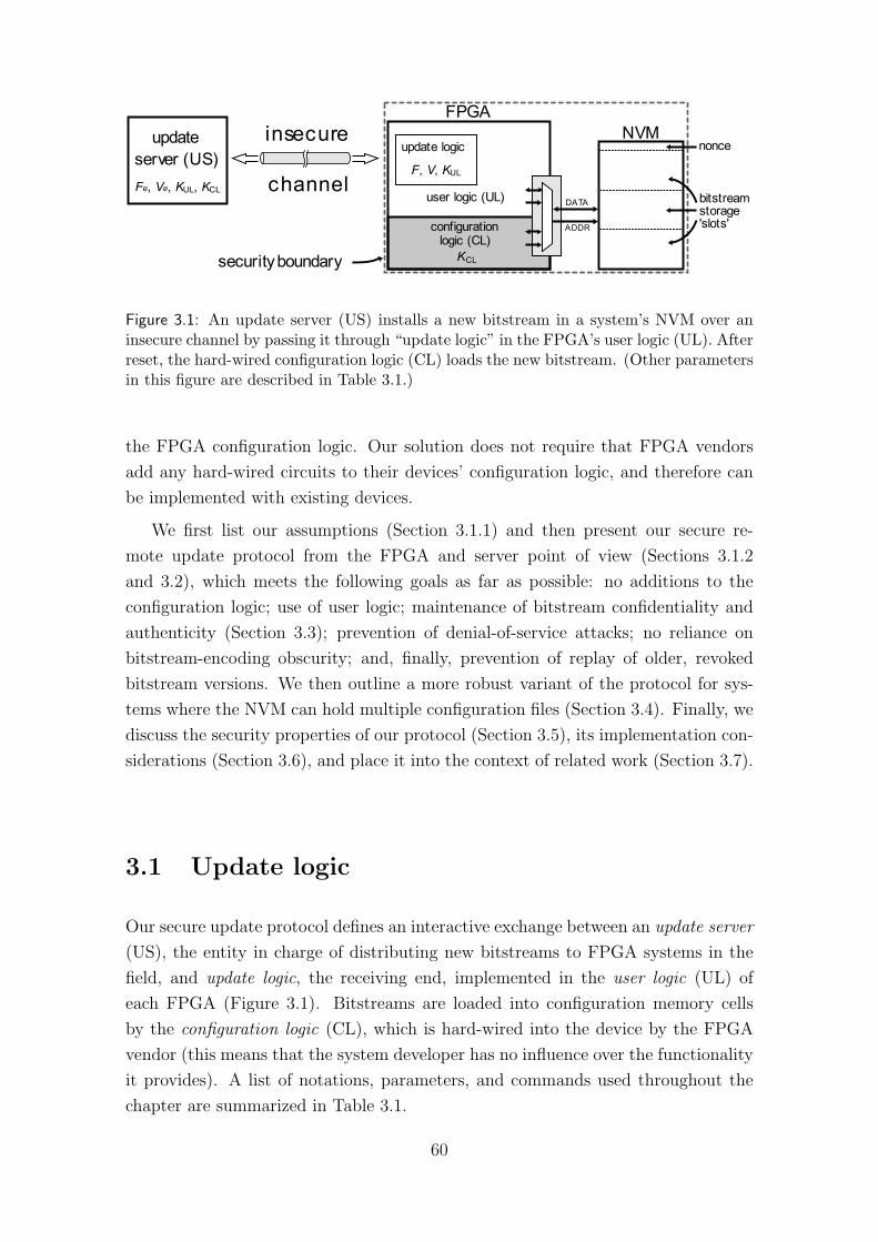
insecure
channel
updateserver (US)
NVMFPGA
user logic (UL) bitstreamstorage'slots'
DATA
ADDRconfigurationlogic (CL)
update logic nonce
security boundary
Fe, Ve, KUL, KCL
KCL
F, V, KUL
Figure 3.1: An update server (US) installs a new bitstream in a system’s NVM over aninsecure channel by passing it through “update logic” in the FPGA’s user logic (UL). Afterreset, the hard-wired configuration logic (CL) loads the new bitstream. (Other parametersin this figure are described in Table 3.1.)
the FPGA configuration logic. Our solution does not require that FPGA vendors
add any hard-wired circuits to their devices’ configuration logic, and therefore can
be implemented with existing devices.
We first list our assumptions (Section 3.1.1) and then present our secure re-
mote update protocol from the FPGA and server point of view (Sections 3.1.2
and 3.2), which meets the following goals as far as possible: no additions to the
configuration logic; use of user logic; maintenance of bitstream confidentiality and
authenticity (Section 3.3); prevention of denial-of-service attacks; no reliance on
bitstream-encoding obscurity; and, finally, prevention of replay of older, revoked
bitstream versions. We then outline a more robust variant of the protocol for sys-
tems where the NVM can hold multiple configuration files (Section 3.4). Finally, we
discuss the security properties of our protocol (Section 3.5), its implementation con-
siderations (Section 3.6), and place it into the context of related work (Section 3.7).
3.1 Update logic
Our secure update protocol defines an interactive exchange between an update server
(US), the entity in charge of distributing new bitstreams to FPGA systems in the
field, and update logic, the receiving end, implemented in the user logic (UL) of
each FPGA (Figure 3.1). Bitstreams are loaded into configuration memory cells
by the configuration logic (CL), which is hard-wired into the device by the FPGA
vendor (this means that the system developer has no influence over the functionality
it provides). A list of notations, parameters, and commands used throughout the
chapter are summarized in Table 3.1.
60
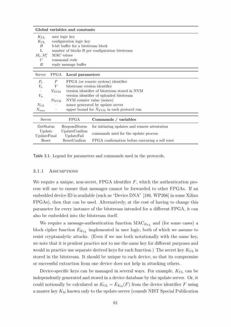
Global variables and constants
KUL user logic keyKCL configuration logic keyB b-bit buffer for a bitstream blockL number of blocks B per configuration bitstream
Mi, M′i MAC values
C command codeR reply message buffer
Server FPGA Local parameters
Fe F FPGA (or remote system) identifierVe V bitstream version identifier– VNVM version identifier of bitstream stored in NVMVu – version identifier of uploaded bitstream– NNVM NVM counter value (nonce)
NUS – nonce generated by update serverNmax – upper bound for NNVM in each protocol run
Server FPGA Commands / variables
GetStatus RespondStatus for initiating updates and remote attestationUpdate UpdateConfirm commands used for the update processUpdateFinal UpdateFailReset ResetConfirm FPGA confirmation before executing a self reset
Table 3.1: Legend for parameters and commands used in the protocols.
3.1.1 Assumptions
We require a unique, non-secret, FPGA identifier F , which the authentication pro-
cess will use to ensure that messages cannot be forwarded to other FPGAs. If an
embedded device ID is available (such as “Device DNA” [186, WP266] in some Xilinx
FPGAs), then that can be used. Alternatively, at the cost of having to change this
parameter for every instance of the bitstream intended for a different FPGA, it can
also be embedded into the bitstream itself.
We require a message-authentication function MACKULand (for some cases) a
block cipher function EKULimplemented in user logic, both of which we assume to
resist cryptanalytic attacks. (Even if we use both notationally with the same key,
we note that it is prudent practice not to use the same key for different purposes and
would in practice use separate derived keys for each function.) The secret key KUL is
stored in the bitstream. It should be unique to each device, so that its compromise
or successful extraction from one device does not help in attacking others.
Device-specific keys can be managed in several ways. For example, KUL can be
independently generated and stored in a device database by the update server. Or, it
could notionally be calculated as KUL = EKM(F ) from the device identifier F using
a master key KM known only to the update server (consult NIST Special Publication
61
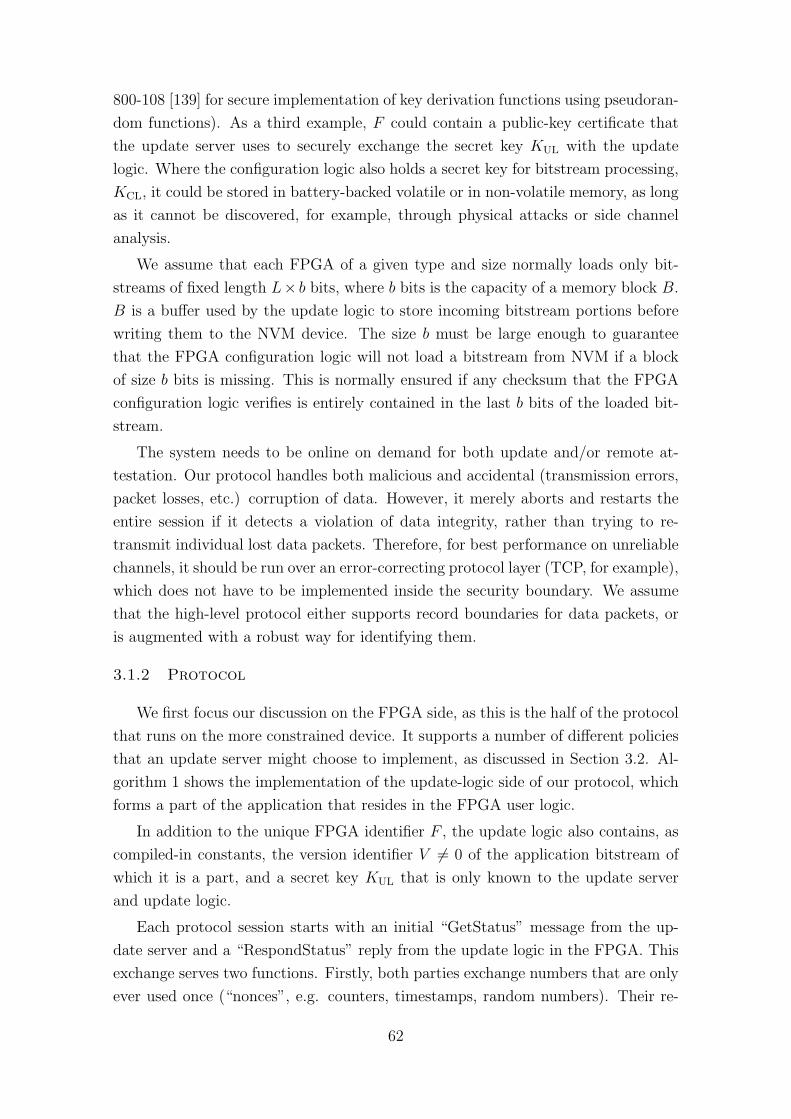
800-108 [139] for secure implementation of key derivation functions using pseudoran-
dom functions). As a third example, F could contain a public-key certificate that
the update server uses to securely exchange the secret key KUL with the update
logic. Where the configuration logic also holds a secret key for bitstream processing,
KCL, it could be stored in battery-backed volatile or in non-volatile memory, as long
as it cannot be discovered, for example, through physical attacks or side channel
analysis.
We assume that each FPGA of a given type and size normally loads only bit-
streams of fixed length L× b bits, where b bits is the capacity of a memory block B.
B is a buffer used by the update logic to store incoming bitstream portions before
writing them to the NVM device. The size b must be large enough to guarantee
that the FPGA configuration logic will not load a bitstream from NVM if a block
of size b bits is missing. This is normally ensured if any checksum that the FPGA
configuration logic verifies is entirely contained in the last b bits of the loaded bit-
stream.
The system needs to be online on demand for both update and/or remote at-
testation. Our protocol handles both malicious and accidental (transmission errors,
packet losses, etc.) corruption of data. However, it merely aborts and restarts the
entire session if it detects a violation of data integrity, rather than trying to re-
transmit individual lost data packets. Therefore, for best performance on unreliable
channels, it should be run over an error-correcting protocol layer (TCP, for example),
which does not have to be implemented inside the security boundary. We assume
that the high-level protocol either supports record boundaries for data packets, or
is augmented with a robust way for identifying them.
3.1.2 Protocol
We first focus our discussion on the FPGA side, as this is the half of the protocol
that runs on the more constrained device. It supports a number of different policies
that an update server might choose to implement, as discussed in Section 3.2. Al-
gorithm 1 shows the implementation of the update-logic side of our protocol, which
forms a part of the application that resides in the FPGA user logic.
In addition to the unique FPGA identifier F , the update logic also contains, as
compiled-in constants, the version identifier V 6= 0 of the application bitstream of
which it is a part, and a secret key KUL that is only known to the update server
and update logic.
Each protocol session starts with an initial “GetStatus” message from the up-
date server and a “RespondStatus” reply from the update logic in the FPGA. This
exchange serves two functions. Firstly, both parties exchange numbers that are only
ever used once (“nonces”, e.g. counters, timestamps, random numbers). Their re-
62
Algorithm 1 Update-logic state machine: FPGA
1: VNVM := V2: Receive(C, Ve, Fe, Nmax, NUS, M0)3: if C 6= “GetStatus” then goto 24: ReadNVMN(NNVM)5: S := [M0 = MACKUL
(C, Ve, Fe, Nmax, NUS)] ∧(Ve = V ) ∧ (Fe = F ) ∧ (NNVM < Nmax)
6: if S then7: NNVM := NNVM + 18: WriteNVMN(NNVM)9: end if
10: M1 := MACKUL(“RespondStatus”, V, F, NNVM, VNVM, M0)
11: Send(“RespondStatus”, V, F, NNVM, VNVM, M1)12: if ¬S then goto 213: Receive(C, M ′
0)14: if M ′
0 6= MACKUL(C, M1) then goto 2
15: if C = “Update” then16: VNVM := 017: for i := 1 to L do18: WriteNVMB[i](0)19: end for20: for i := 1 to L do21: Receive(Bi)22: M ′
i := MACKUL(Bi, M
′i−1)
23: if i < L then24: WriteNVMB[i](Bi)25: end if26: end for27: Receive(“UpdateFinal”, Vu, M2)28: if M2 = MACKUL
(“UpdateFinal”, Vu, M′L) then
29: WriteNVMB[L](BL)30: VNVM := Vu
31: R := (“UpdateConfirm”)32: else33: R := (“UpdateFail”)34: end if35: M3 := MACKUL
(R, M2);36: Send(R, M3)37: else if C = “Reset” then38: M2 := MACKUL
(“ResetConfirm”, M ′0);
39: Send(“ResetConfirm”, M2)40: ResetFPGA()41: end if42: goto 2
63

ception is cryptographically confirmed by the other party in subsequent messages.
Such challenge-response round trips enable each party to verify the freshness of any
subsequent data packet received, and thus protect against replay attacks. The nonce
NUS, generated by the update server, must be an unpredictable random number that
has a negligible chance of ever repeating. This makes it infeasible for attackers to
create a dictionary of FPGA replies. The nonce NNVM contributed by the update
logic is a monotonic counter maintained in NVM (avoiding the difficulties of im-
plementing a reliable and trusted source of randomness or time within the security
boundary). To protect this counter against attempts to overflow it, and also to pro-
tect against attempts to wear out NVM that only lasts a limited number of write
cycles, the update logic will only increment it when authorized to do so by the up-
date server. For this reason, the update server includes in the “GetStatus” message
an upper bound Nmax (of the same unsigned integer type as NNVM) beyond which
the NVM counter must not be incremented in response to this message. The proto-
col cannot proceed past the “RespondStatus” message unless the NVM counter is
incremented.
The second purpose of the initial exchange is to ensure that both parties agree
on values of F and V . The update server sends its expected values Ve and Fe,
and the update logic will not proceed beyond the “RespondStatus” message un-
less these values match its own V and F . This ensures that an attacker cannot
reuse any “GetStatus” message intended for one particular FPGA chip F and in-
stalled bitstream version V on any other such combination. The update server
might know V and F already from a database that holds the state of all fielded
systems. If this information is not available, the update server can gain it in a prior
“GetStatus”/“RespondStatus” exchange, because both values are reported and au-
thenticated in the “RespondStatus” reply.
All protocol messages are authenticated using a message-authentication code
(MAC) computed with the shared secret key KUL. This is done in order to ensure
that an attacker cannot generate any message that has not been issued by the update
server or update logic. In addition, with the exception of the initial “GetStatus”
message, the calculation of the MAC for each message in a protocol session incor-
porates not only all data bits of the message, but also the MAC of the previously
received message. This way, each MAC ensures at any step of the protocol that
both parties agree not only on the content of the current message, but also on the
content of the entire protocol session so far. This mechanism makes it unnecessary
to repeat in messages any data (nonces, version identifiers, etc.) that has been
previously transmitted, because their values are implicitly carried forward in each
message by the MAC chain. Note that in the presentation of Algorithm 1, M , M ′
and B are registers, not arrays, and their indices merely indicate different values
64
that they store during the execution of one protocol session. The indices of NVM
read and write commands (e.g., WriteNVMB[i] and ReadNVMN) indicate addresses.
Any “GetStatus” request results in a “RespondStatus” reply, even without a
correct MAC M0. This is to allow update servers to query F even before knowing
which KUL to apply. However, an incorrect “GetStatus” MAC will prevent the ses-
sion from proceeding beyond the “RespondStatus” reply. This means that anyone
can easily query the bitstream version identifier V from the device. If this is of con-
cern because, for example, it might allow an attacker to quickly scan for vulnerable
old versions in the field, then the value V used in the protocol can be an individually
encrypted version of the actual version number V , as in V = EKUL(V ). Whether
this option is used or not does not affect the update-logic implementation of the
protocol, which treats V just as an opaque identifier bitstring.
The protocol can only proceed beyond the “RespondStatus” message if the
update-logic nonce has been incremented and both sides agree on which FPGA
and bitstream version is being updated. If the update server decides to proceed, it
will continue the session with a command that instructs the update logic either to
begin programming a new bitstream into NVM (“Update”), or to reset the FPGA
and reload the bitstream from NVM (“Reset”). The MAC M ′0 of this command will
depend on the MAC M1 of the preceding “RespondStatus” message, which in turn
depends on the freshly incremented user-logic nonce NNVM, as well as V and F .
Therefore, the verification of M ′0 ensures the user-logic of both the authenticity and
the freshness of this command, and the same applies to all MAC verifications in the
rest of the session.
The successful authentication of the “Update” command leads to erasing the
entire bitstream from the NVM. From this point on, until all blocks B1 to BL have
been written, the NVM will not contain a valid bitstream. Therefore, there is no
benefit in authenticating each received bitstream data block Bi individually before
writing it into NVM. Instead, we postpone the writing of the last bitstream block
BL into NVM until the “UpdateFinal” command MAC M ′L that covers the entire
bitstream has been verified. This step is finally confirmed by the update logic in an
“UpdateConfirm” – or in case of failure, “UpdateFail” – message.
If no messages were lost, the update server will receive an authenticated confirma-
tion. “UpdateConfirm” indicates that the “Update” command has been processed,
and its MAC M3 confirms each received data byte, as well as the old and new version
identifiers, FPGA ID, nonces, and any other data exchanged during the session. The
“ResetConfirm” command can only confirm that the reset of the FPGA is about to
take place; any attestation of the successful completion of the reset must be left to
the new bitstream.
65

3.1.3 Recovery from errors
Since a system that can store only a single bitstream in its NVM must not be reset
before all blocks of the bitstream have been uploaded, our protocol also provides an
authenticated status indicator VNVM intended to help recover from protocol sessions
that were aborted due to loss or corruption of messages. After a successful reset,
the update logic sets VNVM := V to indicate the version identifier of the bitstream
stored in NVM. Before the process of erasing and rewriting the NVM begins, it sets
VNVM to the reserved value 0, to indicate the absence of a valid bitstream in NVM.
With message “UpdateFinal”, after the last block BL has been written, the update
logic receives from the update server the version identifier Vu of the bitstream that
has just been uploaded into NVM, and sets register VNVM accordingly. Should the
update session be aborted for any reason, then the update server can always initiate
a new session with a new “GetStatus”/“RespondStatus” exchange. The update
server will learn from the VNVM value in the “RespondStatus” message the current
status of the NVM: whether the old bitstream is still intact, the new bitstream has
been uploaded completely, or it contains no valid bitstream. The update server can
then decide whether to attempt a new upload or perform a reset.
3.2 Update server routines
Algorithm 2 Server-side update routine UpdateServer
1: Fe := Get(“FPGA/system ID”) or ‘0’ if unknown2: Ve := Get(“current version”, Fe) or ‘0’ if unknown3: KUL := Get(“update logic key”, Fe, Ve) or ‘0’ if unknown4: Nmax := Get(“NNVM”, Fe) or ‘0’ if unknown5: task := “updateAndReset”6: Handshake
7: while KUL = 0 do8: EstablishKey
9: end while10: loop11: UpdateOrReset
12: end loop
Algorithm 3 Server: subroutine Handshake
1: Generate(NUS)2: M0 = MACKUL
(“GetStatus”, Ve, Fe, Nmax, NUS)3: Send(“GetStatus”, Ve, Fe, Nmax, NUS, M0)4: Receive(“RespondStatus”, V, F, NNVM, VNVM, M1)
66
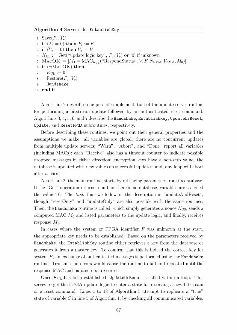
Algorithm 4 Server-side: EstablishKey
1: Save(Fe, Ve)2: if (Fe = 0) then Fe := F3: if (Ve = 0) then Ve := V4: KUL := Get(“update logic key”, Fe, Ve) or ‘0’ if unknown5: MacOK := [M1 = MACKUL
(“RespondStatus”, V, F, NNVM, VNVM, M0)]6: if (¬MacOK) then7: KUL := 08: Restore(Fe, Ve)9: Handshake
10: end if
Algorithm 2 describes one possible implementation of the update server routine
for performing a bitstream update followed by an authenticated reset command.
Algorithms 3, 4, 5, 6, and 7 describe the Handshake, EstablishKey, UpdateOrReset,
Update, and ResetFPGA subroutines, respectively.
Before describing these routines, we point out their general properties and the
assumptions we make: all variables are global; there are no concurrent updates
from multiple update servers; “Warn”, “Abort”, and “Done” report all variables
(including MACs); each “Receive” also has a timeout counter to indicate possible
dropped messages in either direction; encryption keys have a non-zero value; the
database is updated with new values on successful updates; and, any loop will abort
after n tries.
Algorithm 2, the main routine, starts by retrieving parameters from its database.
If the “Get” operation returns a null, or there is no database, variables are assigned
the value ‘0’. The task that we follow in the description is “updateAndReset”,
though “resetOnly” and “updateOnly” are also possible with the same routines.
Then, the Handshake routine is called, which simply generates a nonce NUS, sends a
computed MAC M0 and listed parameters to the update logic, and finally, receives
response M1.
In cases where the system or FPGA identifier F was unknown at the start,
the appropriate key needs to be established. Based on the parameters received by
Handshake, the EstablishKey routine either retrieves a key from the database or
generates it from a master key. To confirm that this is indeed the correct key for
system F , an exchange of authenticated messages is performed using the Handshake
routine. Transmission errors would cause the routine to fail and repeated until the
response MAC and parameters are correct.
Once KUL has been established, UpdateOrReset is called within a loop. This
serves to get the FPGA update logic to enter a state for receiving a new bitstream
or a reset command. Lines 1 to 18 of Algorithm 5 attempt to replicate a “true”
state of variable S in line 5 of Algorithm 1, by checking all communicated variables.
67
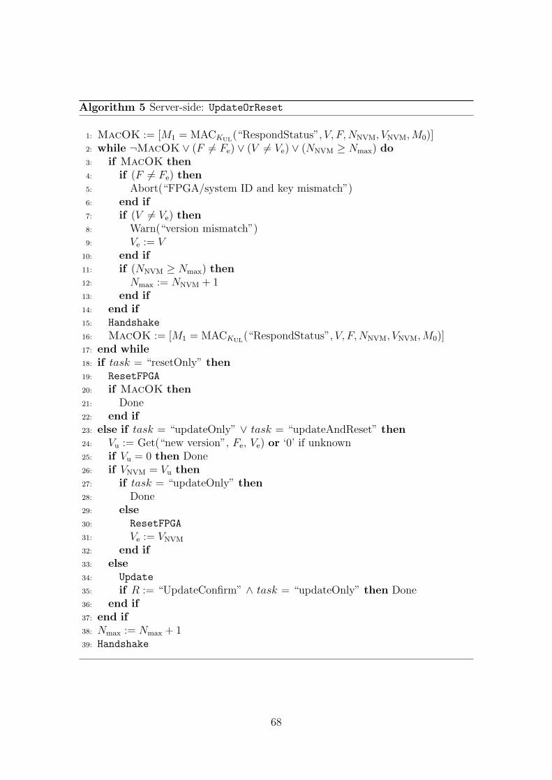
Algorithm 5 Server-side: UpdateOrReset
1: MacOK := [M1 = MACKUL(“RespondStatus”, V, F, NNVM, VNVM, M0)]
2: while ¬MacOK ∨ (F 6= Fe) ∨ (V 6= Ve) ∨ (NNVM ≥ Nmax) do3: if MacOK then4: if (F 6= Fe) then5: Abort(“FPGA/system ID and key mismatch”)6: end if7: if (V 6= Ve) then8: Warn(“version mismatch”)9: Ve := V
10: end if11: if (NNVM ≥ Nmax) then12: Nmax := NNVM + 113: end if14: end if15: Handshake
16: MacOK := [M1 = MACKUL(“RespondStatus”, V, F, NNVM, VNVM, M0)]
17: end while18: if task = “resetOnly” then19: ResetFPGA
20: if MacOK then21: Done22: end if23: else if task = “updateOnly” ∨ task = “updateAndReset” then24: Vu := Get(“new version”, Fe, Ve) or ‘0’ if unknown25: if Vu = 0 then Done26: if VNVM = Vu then27: if task = “updateOnly” then28: Done29: else30: ResetFPGA
31: Ve := VNVM
32: end if33: else34: Update
35: if R := “UpdateConfirm” ∧ task = “updateOnly” then Done36: end if37: end if38: Nmax := Nmax + 139: Handshake
68
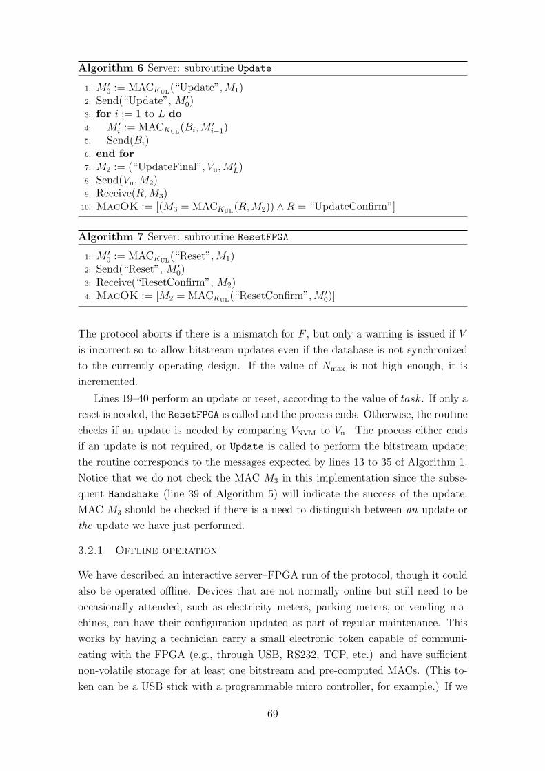
Algorithm 6 Server: subroutine Update
1: M ′0 := MACKUL
(“Update”, M1)2: Send(“Update”, M ′
0)3: for i := 1 to L do4: M ′
i := MACKUL(Bi, M
′i−1)
5: Send(Bi)6: end for7: M2 := (“UpdateFinal”, Vu, M
′L)
8: Send(Vu, M2)9: Receive(R, M3)
10: MacOK := [(M3 = MACKUL(R, M2)) ∧R = “UpdateConfirm”]
Algorithm 7 Server: subroutine ResetFPGA
1: M ′0 := MACKUL
(“Reset”, M1)2: Send(“Reset”, M ′
0)3: Receive(“ResetConfirm”, M2)4: MacOK := [M2 = MACKUL
(“ResetConfirm”, M ′0)]
The protocol aborts if there is a mismatch for F , but only a warning is issued if V
is incorrect so to allow bitstream updates even if the database is not synchronized
to the currently operating design. If the value of Nmax is not high enough, it is
incremented.
Lines 19–40 perform an update or reset, according to the value of task. If only a
reset is needed, the ResetFPGA is called and the process ends. Otherwise, the routine
checks if an update is needed by comparing VNVM to Vu. The process either ends
if an update is not required, or Update is called to perform the bitstream update;
the routine corresponds to the messages expected by lines 13 to 35 of Algorithm 1.
Notice that we do not check the MAC M3 in this implementation since the subse-
quent Handshake (line 39 of Algorithm 5) will indicate the success of the update.
MAC M3 should be checked if there is a need to distinguish between an update or
the update we have just performed.
3.2.1 Offline operation
We have described an interactive server–FPGA run of the protocol, though it could
also be operated offline. Devices that are not normally online but still need to be
occasionally attended, such as electricity meters, parking meters, or vending ma-
chines, can have their configuration updated as part of regular maintenance. This
works by having a technician carry a small electronic token capable of communi-
cating with the FPGA (e.g., through USB, RS232, TCP, etc.) and have sufficient
non-volatile storage for at least one bitstream and pre-computed MACs. (This to-
ken can be a USB stick with a programmable micro controller, for example.) If we
69

NVMFPGA
user logic operatingdesign
DATA
ADDR
configuration logic
MAC
FPGA
user logicDATA
ADDR
MAC
DEC
NVM
operating design
encryptedwith
CL: no decryption or authentication CL: decryption without authentication
NNVM NNVM
KCL KCL
DECbufferB
bufferB
configuration logic
F, V, KUL F, V, KUL
FPGA
user logicDATA
ADDR
MAC
DEC +MAC
NVM
CL: decryption and authentication
operating design
encrypted +authenticated
with
NNVM
KCL KCL
bufferB
configuration logic
F, V, KUL
Figure 3.2: Scenarios for different configuration logic (CL) capabilities.
assume that the actual and expected values of NNVM are the same, the update server
can pre-compute a complete protocol run and load it onto the token. Then, when
a technician inserts the token into the FPGA system it behaves just like a server,
but instead of computing MACs it sends and compares to stored ones. When the
update is complete, the token performs a handshake (with Nmax = 0) and stores the
“RespondStatus” message and MAC M1 so the server can verify it and synchronize
itself to the status of the FPGA system. Note that since the token is not required to
compute MACs it can be a simple device, but more importantly, it is not required
to store any secret keys.
In the case where NNVM may not be synchronized, the update server may choose
to pre-compute several protocol runs for values of NNVM between the lowest expected
value of NNVM and Nmax. This simply means that the token is now required to have
additional storage for these MACs1.
3.3 Authenticity and confidentiality
As we discussed in Sections 2.3.1 and 2.3.2, some FPGAs can decrypt bitstreams
in their configuration logic, using embedded (or battery-backed) keys, while others
1With task := “updateAndReset”, Algorithm 2 generates six MACs (M0, M0, M ′0, M2, M0, M ′
0)and the update logic five MACs (M1, M1, M3, M1, M2). The update logic MACs can be storedfor debug purposes, as well as two additional MACs (M0, M1) for another call of Handshake.
70

lack this capability; we have also discussed proposals for bitstream authentication in
Section 2.3.2. Our protocol can be used with FPGAs that support any combination
of these functions, as shown in Figure 3.2, provided that the user logic compensates
for those functions that are missing.
For confidentiality, bitstreams should always be transmitted encrypted between
the update server and update logic. Where the configuration logic is able to de-
crypt a bitstream while loading it from NVM, the update server can encrypt the
bitstream under a secret key KCL shared with the configuration logic, leaving the
update logic and NVM merely handling ciphertext. If the configuration logic can-
not decrypt, the update server has to encrypt the bitstream under a key derived
from KUL and the user logic has to decrypt each block Bi before writing it to NVM
(using some standard file encryption method, such as cipher-block chaining). If
the configuration logic also supports authentication, the requirements above do not
change; the authentication performed by the update logic is still necessary to prevent
denial-of-service attacks that attempt unauthorized overwriting of NVM content. As
before, the last buffered block BL must contain the MAC of the bitstream that the
configuration logic will verify, such that the bitstream will not load without the
successful verification of M2.
3.4 Multiple NVM slots
NVM devices that provide only a single memory location (“slot”) for storing a
bitstream can seriously limit the reliability of the system. There will be no valid
bitstream stored in the NVM from when the update logic starts erasing the NVM
until it has completed writing the new bitstream. A malicious or accidental inter-
ruption, such as a power failure or a long delay in the transmission of the remaining
bitstream, can leave the system in an unrecoverable state. Such single-slot systems
are, therefore, only advisable where loss of communications or power is unlikely,
such as with local updates with a secure and reliable power source.
Otherwise, the NVM should provide at least two slots, such that it can hold both
the old and the new bitstream simultaneously. The FPGA configuration logic will
then have to scan through these NVM slots until it encounters a valid bitstream.
It will start loading a bitstream from the first slot. If the bitstream is invalid (i.e.,
has an incorrect checksum or MAC), it will load another bitstream from the next
slot, continuing until all slots have been tried or a valid one has been found. The
additional slot is then used during the update as a temporary store, in order to
preserve the currently operating design in case of an update failure. The role of the
two slots – upload area and operating bitstream store – alternate between updates,
depending on how multiple slots are supported by the configuration logic.
71
The update process may be modified as follows. At manufacturing, slot 1 is
loaded with an initial design whose update logic can only write new bitstreams into
the address space of slot 2. Before the VNVM := Vu changeover is made (line 30 of
Algorithm 1), the update logic erases slot 1, which then allows the configuration
logic to find the new bitstream in slot 2 at the next power-up. The new bitstream,
now in slot 2, will write its next bitstream into slot 1, and erases slot 2 when that
update is complete, and so on. If an update is aborted by reset, one slot may contain
a partially uploaded bitstream. If this is slot 1, the configuration logic will fail to
find a correct checksum there and move on to load the old bitstream from slot 2,
from where the update process can then be restarted2. If the partial content is in
slot 2, then the configuration logic will never get there because the bitstream in
slot 1 will be loaded first.
If the configuration logic tells the update logic which slot it came from (through
status registers), then the user logic can simply pick the respective other slot and
there is no need to compile a unique bitstream for each slot. If not, then the update
server must ensure, through remote attestation, that each newly updated bitstream
is compiled to write the next bitstream to the respective other slot. This might be
aided by encoding in V which slot a bitstream was intended for. A third slot may
store a fallback bitstream that is never overwritten, and only loaded if something
goes wrong during the NVM write process without the update logic noticing (e.g.
data corruption between the FPGA and the NVM). This could leave both slot 1
and 2 without a valid bitstream and cause the fallback bitstream to be loaded
from slot 3. Alternatively, the FPGA may always load, as a first configuration, a
bootloader bitstream that controls which slot the next bitstream is loaded from.
Recent FPGAs, such as Virtex-5 [186, UG191 ch8, “Fallback MultiBoot”] or
LatticeECP2/M [120, TN1148, “SPIm Mode”], implement a multi-slot scan in the
configuration logic. Some, including Stratix IV [7, SIV51010-2.0, “Remote System
Upgrade Mode”] or Virtex-5 [186, UG191 ch8, “IPROG Reconfiguration”], provide
a “(re)load bitstream from address X” command register, or bitstream command,
so that a user-designed bootloader bitstream can implement a multi-slot scan and
checksum verification (but such a bootloader itself cannot necessarily be updated
remotely).
Figure 3.3 shows how this can work with a Virtex-5 FPGA. Starting at address 0,
the configuration logic processes a short header and then encounters an address
2An update can be aborted in various places, so as described, a simple scan may not alwayswork. We have experimented with a Virtex-5 FPGA to test if it can load a complete bitstreamthat is stored after an incomplete one in NVM. It failed. We think that this is because theinternal configuration state machine may not be able to recover from abrupt de-synchronizationof configuration data. It would be helpful if FPGA vendors provided a reliable way to do that,perhaps by using re-synchronization words that are placed in between bitstream slots, and arenever changed during the update process.
72

VNVM ADDR NNVM
bitstream slot 2
SLOT 2 ADDR
bitstream slot 1
SLOT 1 ADDR
IPROG
WBSTAR ADDR WBSTAR address assignment
bitstream header information
0
“goto”addressWBSTAR
(fixedbootloader)
Figure 3.3: Memory map for the NVM with two bitstream slots. When the configurationlogic encounters the IPROG command it jumps to address WBSTAR to search for a newbitstream. This mechanism allows the update logic to change the content of WBSTAR sobitstreams from any slot are loaded on power-up. The NNVM nonce is stored at the topaddress of the NVM so it does not interfere with the loading of bitstreams.
assignment into the WBSTAR register followed by a “goto” command, IPROG.
This causes the configuration logic to jump to that address and continue searching
for a bitstream there. SLOT 1 ADDR and SLOT 2 ADDR are compiled-in parameters in
the update logic, so when an update starts it can read the content of WBSTAR from
the NVM and know from which slot it was loaded from. It now knows to which
slot the new bitstream should be written to as well, and after a successful update
the content of address WBSTAR ADDR is updated with the start address of the new
bitstream’s slot. During the write of the address to NVM, the system will not be
able to recover if power is lost because the configuration logic will not be able to load
a valid bitstream. A possible solution is to use a bootloader that checks the NVM
for valid bitstreams (using CRC, for example, and knowledge of the bitstream size)
before issuing the WBSTAR command. A more expensive alternative for FPGAs
without such multi-slot support is to include a configuration manager device, such
as SystemAce [186, DS080] or a non-volatile PLD, inside of the security boundary.
73
3.5 Analysis
Algorithm 1 alone cannot prevent the configuration logic from loading old bitstreams
from NVM. In order to maintain our security objective of preventing attackers from
operating older and outdated FPGA configurations, we also need to rely on either
tamper proofing or binding the provision of online services to remote attestation.
With Algorithm 1, if attackers can either feed the FPGA with NNVM values of
previously recorded sessions, or have access to its configuration port, they can replay
older bitstreams. Therefore, these interfaces must be protected: the FPGA, NVM
and the interface between them (configuration and read/write) must be contained
within a tamper-proof enclosure. Manufacturing effective tamper-proof enclosures
can be challenging [58, 158], although there are now a number of strong off-the-shelf
solutions available3, such as tamper-sensing membranes and security supervisor chips
that trigger zeroization of keys stored in battery-backed SRAM when penetrated.
That said, protection against highly capable attackers is not necessary for all
applications. Sometimes, it may suffice to deter attackers by using ball-grid ar-
ray packages and routing security-critical signals entirely in internal printed circuit
board layers (“stripline”) without accessible vias (“buried”); some passive compo-
nents can even be embedded or created between internal printed circuit board lay-
ers [39, ch21]. Some manufacturers may not be concerned if a few of their systems
are maliciously downgraded with great effort in a laboratory environment, as long
as the financial damage of the attack remains limited and it is impractical to scale it
up by creating a commercial low-cost kit that allows everyone to repeat the attack
with ease. For example, in consumer electronics, an attractive attack cannot require
risky precision drilling into a printed circuit board or de-soldering a fine-pitch ball-
grid array, especially for relatively expensive consumer products. New stacked-die
products, where the NVM is attached to the top of the FPGA die inside the same
package (such as the Xilinx Spartan-3AN family [186, UG331]) also make tamper
proofing easier.
In some applications, the device’s only use is to provide a service by interacting
with a central server. For those types of products, the provision of the service can
be made conditional to a periodic successful remote attestation of the currently
operating bitstream, in order to render the device inoperable unless it has an up-to-
date bitstream loaded in the NVM. A remote attestation facility can give the service
provider assurances of configuration authenticity even where no tamper proofing
exists, though the system must be periodically online (set-top boxes are a good
example).
3One example of a circuit board enclosure is the “GORE Tamper Respondent Surface Enclosure”,though we have not personally evaluated its security claims.http://www.gore.com/MungoBlobs/612/1006/surface_enclosure.pdf
74
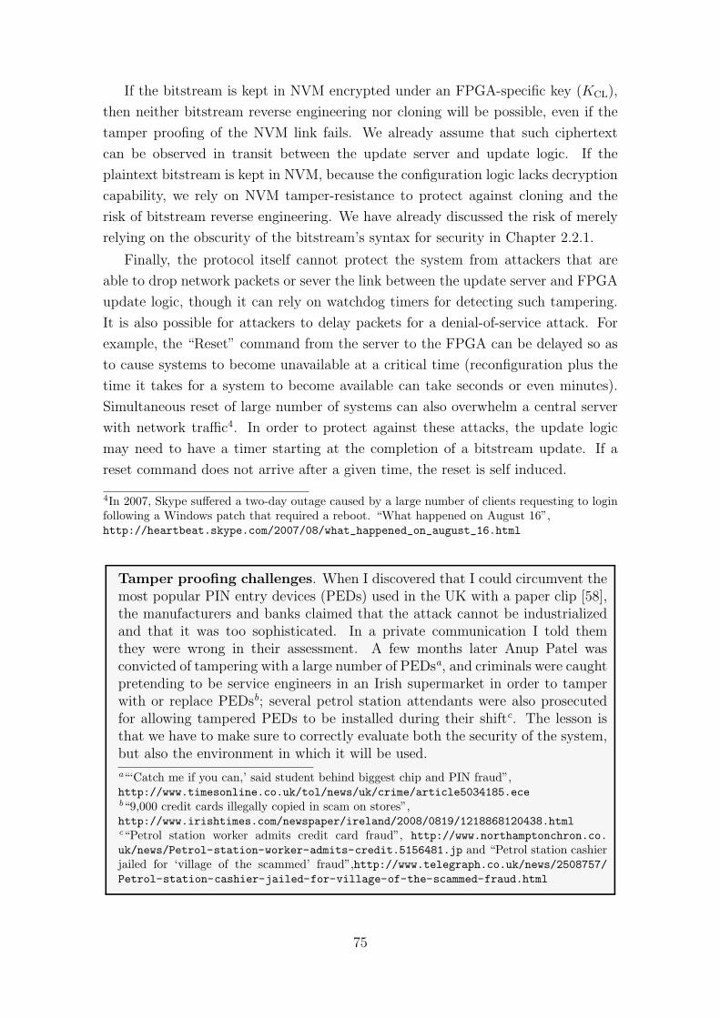
If the bitstream is kept in NVM encrypted under an FPGA-specific key (KCL),
then neither bitstream reverse engineering nor cloning will be possible, even if the
tamper proofing of the NVM link fails. We already assume that such ciphertext
can be observed in transit between the update server and update logic. If the
plaintext bitstream is kept in NVM, because the configuration logic lacks decryption
capability, we rely on NVM tamper-resistance to protect against cloning and the
risk of bitstream reverse engineering. We have already discussed the risk of merely
relying on the obscurity of the bitstream’s syntax for security in Chapter 2.2.1.
Finally, the protocol itself cannot protect the system from attackers that are
able to drop network packets or sever the link between the update server and FPGA
update logic, though it can rely on watchdog timers for detecting such tampering.
It is also possible for attackers to delay packets for a denial-of-service attack. For
example, the “Reset” command from the server to the FPGA can be delayed so as
to cause systems to become unavailable at a critical time (reconfiguration plus the
time it takes for a system to become available can take seconds or even minutes).
Simultaneous reset of large number of systems can also overwhelm a central server
with network traffic4. In order to protect against these attacks, the update logic
may need to have a timer starting at the completion of a bitstream update. If a
reset command does not arrive after a given time, the reset is self induced.
4In 2007, Skype suffered a two-day outage caused by a large number of clients requesting to loginfollowing a Windows patch that required a reboot. “What happened on August 16”,http://heartbeat.skype.com/2007/08/what_happened_on_august_16.html
Tamper proofing challenges. When I discovered that I could circumvent themost popular PIN entry devices (PEDs) used in the UK with a paper clip [58],the manufacturers and banks claimed that the attack cannot be industrializedand that it was too sophisticated. In a private communication I told themthey were wrong in their assessment. A few months later Anup Patel wasconvicted of tampering with a large number of PEDsa, and criminals were caughtpretending to be service engineers in an Irish supermarket in order to tamperwith or replace PEDsb; several petrol station attendants were also prosecutedfor allowing tampered PEDs to be installed during their shiftc. The lesson isthat we have to make sure to correctly evaluate both the security of the system,but also the environment in which it will be used.
a“‘Catch me if you can,’ said student behind biggest chip and PIN fraud”,http://www.timesonline.co.uk/tol/news/uk/crime/article5034185.eceb“9,000 credit cards illegally copied in scam on stores”,http://www.irishtimes.com/newspaper/ireland/2008/0819/1218868120438.htmlc“Petrol station worker admits credit card fraud”, http://www.northamptonchron.co.uk/news/Petrol-station-worker-admits-credit.5156481.jp and “Petrol station cashierjailed for ‘village of the scammed’ fraud”,http://www.telegraph.co.uk/news/2508757/Petrol-station-cashier-jailed-for-village-of-the-scammed-fraud.html
75
FPGA
AESCMAC
NVMNNVM
FIFO(BRAM)
Flashcontrol
AES CBC
mainstate
control
ICAPcontrol
commcontrol
Figure 3.4: The main components of the update logic. Arrows show data flow, solid forconfiguration data input and dashed for command output; for clarity, control signals arenot shown. The multiplexer in the gray box indicates dual-purpose I/Os that are controlledby the configuration logic during configuration and later by the user logic. AES in CBCmode may be used for processing encrypted incoming bitstreams when the configurationlogic is not capable of bitstream decryption.
3.6 Implementation considerations
Figure 3.4 shows one possible implementation of the update protocol in user logic;
this can be implemented in “logic”, or using a soft- or hard-core embedded pro-
cessor. FPGA implementations for receiving bitstreams and writing them to an
external non-volatile memory already exist [186, AN441], so are outside the scope
of this chapter. Instead, we will discuss the aspects that affect the security of an
implementation.
3.6.1 Parameter sizes
As the NVM counter NNVM is well protected against overflow attacks by the Nmax
parameter (controlled by the update server), a size of 32 bits appears to be more than
sufficient for most applications. Since an attacker can keep asking for a response
for any value of NUS, it should be large enough to make the creation of a dictionary
of responses that can be replayed impractical. For instance, using a uniformly
distributed 64 bit word for NUS will ensure that an attacker who performs 103 queries
per second will fill less than 10−7 of the dictionary within a decade. MAC values
(M , M ′) of 64 bit length provide an equally generous safety margin to brute-force
upload attempts. Other fields’ sizes (V , F , CMD) depend on the application.
In Section 3.1.1 we defined B as the minimum size of bitstream portion that when
absent would cause the configuration logic not to load the bitstream. Implicitly, it
also meant that B is the size of the buffer for storing the last block BL, before
authenticating the entire bitstream. In practice, however, the size of the buffer can
76
be larger than B, limited only by the availability of embedded RAM in user logic.
Other considerations may be the smallest block size that can be written efficiently
into NVM, and the block size of the MAC’s compression function (some NVM devices
allow block-writes that are faster than writing into individual addresses separately).
A simple way to implement the buffer is to use a BlockRAM-based FIFO connected
to the communication interface (or decryptor output) on one port, and the NVM
interface on the other.
Assuming CMAC [139, SP800-38B] as the MAC function, we should also consider
the “message span” of the MAC key – the maximum amount of blocks that can be
processed with any one key with negligible chance of collisions. Assuming that
each update is followed by a reset, NNVM allows up to 231 updates when Nmax is
incremented by one. The largest Xilinx Virtex-5 FPGA is the LX330 with 82,696,192
bitstream bits [186, UG191, v3.6 t1-4]; conservatively, allowing for future larger
FPGAs, let us assume a size of 227 bits. Thus, each update may consist of up to 220
128-bit input blocks (plus a negligible number of authenticated commands). The
CMAC specification recommends that no more than 248 blocks be processed with
a single key [139, SP800-38B, p13], which, for our application means 248/220 = 228
bitstream updates. It follows that under the (very conservative) conditions above,
a re-key of KUL should occur before the NNVM is exhausted. Re-keying is easy with
our protocol, as each new updated bitstream can contain a new KUL.
The practical limit for the number of updates, however, is likely to be imposed
by the storage media. Typical NOR Flash, for example, is rated for 100 K or 1 M
write cycles (Intel StrataFlash P30 [91] and Spansion S29CD/L5 are examples). If
this limit is of concern we suggest allocating multiple storage addresses for NNVM,
so its range is split (e.g. every 216 increments). The update logic will need to be
able to determine which address to use according to the value of NNVM when it is
read as part of the protocol execution. System developers may also want to create
additional storage slots for when certain amount of updates is exceeded. This could
be done with a large NVM that can store multiple bitstream, though it should be
done with caution in order to avoid the system being left without a valid bitstream,
as we discussed in Section 3.4.
3.7 Related work
The Xilinx “Internet Reconfigurable Logic” initiative from the late 1990s discussed
the potential of remote updates and how they can be performed, though the program
was short lived [186, AN412]. Remote reconfiguration using embedded processors
has also been proposed [186, AN441]. A patent by Trimberger and Conn [173]
5http://www.spansion.com/datasheets/S29CD-J_CL-J_00_B3_e.pdf
77

describes a remote update through a modem, an FPGA controller (in addition to
the main FPGA) and “shadow PROMs” for recovery from failed writes. Altera
describes how field updates can be performed for Stratix and Cyclone devices using
a soft processor in the user logic and a hard logic interface using a non-volatile
memory device, with the ability to revert to a “factory bitstream” stored in the
NVM [7, UG SII52008, SIII51012, SIV51010, CIII51012]. However, the security
aspects of remote update are not considered in any of the above.
Castillo et al. [32] propose a mechanism based on an OpenRISC1200 processor
implemented in the user logic, together with an RSA engine for remote config-
uration on every start-up. However, the cryptographic key on which its security
depends is obfuscated in a non-encrypted bitstream stored in the local NVM. Fong
et al. [66] propose a security controller based on the Blowfish cipher for encryp-
tion and CRC for data correctness. Attached to a “Media Interface”, the FPGA is
able to receive updates that are programmed into the configuration logic through
the internal configuration port. The authors point out the possible vulnerabilities
of their scheme: key obfuscation within the bootstrap bitstream, and more signifi-
cantly, lack of data authentication with freshness, which opens the system to replay
attacks. Both the above schemes require an online connection at start-up to receive
the operating bitstream/design, while ours performs a secure remote update once,
stores the bitstream locally, and programs the FPGA at start-up without online
connectivity.
Replay attacks despite bitstream encryption and authentication were described
in my previous work [51, p21], where I suggested adding a non-volatile counter as
a nonce for bitstream authentication, or remote attestation in user logic as coun-
termeasures. Motivated by this, Badrignans et al. [20] proposed additions to the
hard-coded configuration logic in order to prevent replay of old bitstreams. They
use a nonce in the authentication process, in addition to a mechanism for alerting the
developer of its failure. Our solution of using user-logic resources instead of adding
hard-wired configuration logic functionality is more flexible: our update logic can
also update itself in the field. More importantly, our approach can be used with
existing FPGAs, although it can equally benefit from additional security features in
future ones. We also discuss denial-of-service attacks and failed updates, describe
how the system can recover, and specify the detailed behavior of our update logic
in a way that is ready for implementation.
3.8 Conclusions
We have proposed a secure remote update protocol that maintains the confidential-
ity, integrity and freshness of bitstreams to the extent possible. In contrast to other
78

proposals, our solution requires no additions to the configuration logic of existing
FPGAs and uses the user logic for most security functions. The required crypto-
graphic primitives consume some user-logic resources, but they can be reused by
the main application. Even local attackers can be deterred from restoring old and
outdated bitstreams, which the update server may want to suppress (e.g., due to
known vulnerabilities), by tamper proofing the NVM connection.
The update logic proposed here can be implemented either in software on a
soft processor, or as a logic circuit. The design and presentation of our protocol
was influenced by our experience with an ongoing logic-circuit implementation on
a Virtex-5 evaluation board, using the publicly available AES design described in
Chapter 4.
Possible extensions for the protocol presented here include role- and identity-
based access control (beyond the current single role of “update server”), as well as
receiving online partial configuration content at start-up, to be programmed into
memory cells using an internal configuration port.
79

80
Chapter 4
AES in spare logic
4.1 Introduction
The Advanced Encryption Standard (AES) [139, FIPS-197] is a widely used block
cipher with a rich implementation literature for both software and hardware. Most
AES implementations for reconfigurable devices, however, are based on traditional
configurable logic such as flip-flops and lookup tables (LUTs). Here, we focus on
new embedded functions inside of the Xilinx Virtex-5 FPGA [186, UG190], such as
large dual-ported RAMs and digital signal processing (DSP) blocks [186, UG193]
with the goal of minimizing the use of registers and LUTs so that those may be
used for other functions. Our designs are best suited for applications where most
of the traditional user logic is used by other functions, yet embedded memory and
DSP blocks are still available. Moreover, our design principles may be suitable for
transfer to other course-grain logic devices which consist of multi-core processing
units connected to local memory1. We also focus on the use of embedded functional
blocks that have dedicated routing paths between them. By using these dedicated
paths, we implicitly predefine the relative placement of our AES modules and thus
relax the constraints on the router.
We present three different architectures which are optimized for three application
scenarios. An eight-stage pipeline module (AES32), based on a combination of two
36-Kibit2 BlockRAM (BRAM) and four digital signal processing (DSP) blocks, that
outputs a single 32-bit column of an AES round each cycle. For higher throughput,
AES32 is replicated four times for a full AES round with a 128-bit datapath (AES128).
For a fully unrolled version (AES128U), AES128 is replicated ten times, achieving a
throughput of over 50 Gbit/s. We also describe a separate circuit for pre-computing
1One example is the Tilera TILE64 processor family, http://www.tilera.com/2The unit kibibit, or Kibit for short, equals 210 bits, and is used to avoid the ambiguity of kbitand Kbit. (See “Definitions of the SI units: The binary prefixes”,http://physics.nist.gov/cuu/Units/binary.html)
81

round keys, which can be combined with all three implementations, and report
results from an implementation of the CMAC and CTR modes of operation.
HDL source code and simulation testbenches for the three AES variants and the
CMAC mode of operation are freely available under the “Simplified BSD License”3
from the following URL. We make it available for reuse, evaluation, and reproduction
of the results reported herein:
http://www.cl.cam.ac.uk/~sd410/aes2/ (version 1.0)
4.2 Prior work
Many hardware implementations of AES have been described for FPGAs, ASICs
and software since the U.S. NIST standardized it in 2001. Some are straightforward
implementations of a single AES round or loop-unrolled, pipelined architectures for
FPGAs that use large amounts of user logic [61, 97, 149, 160]. In particular, the
AES 8× 8 S-boxes were mostly implemented in user logic lookup tables (LUT). For
example, Standaert et al. [160] report using 144 4-input-LUTs (4-LUT) for a single
S-box implementation, so using 2,304 LUTs (144 × 16) for a single AES round.
More advanced approaches [33, 35, 132, 160] use embedded memory in FPGAs, but
since capacities were limited in older FPGAs, the majority of implementations only
mapped the 8×8 S-box into the memory while all other AES operations (ShiftRows,
MixColumns and AddRoundKey) were implemented with flip-flops and LUTs.
Reviewing all published AES implementations for FPGAs and ASICs is outside
the scope of this chapter (we refer the interested reader to Jarvinen [96]), so we
will only examine the ones that are closely relevant to the work presented here. We
categorize implementations according to performance, resource consumption, and
datapath widths.
Resource optimized: AES implementations designed for area efficiency are
mostly based on an 8-bit datapath and use shared resources for key expansion and
round computations. An example is Good and Benaissa [72] which requires 124
Xilinx Spartan-II 15(-6) slices and two BRAMs of a for 0.0022 Gbit/s encryption
throughput. Small implementations with 32-bit datapath also exist: the AES im-
plementation of Chodowiec and Gaj [35] on a Xilinx Spartan-II 30(-6) consumes
222 slices and 3 embedded Block RAMs for a 0.166 Gbit/s encryption rate. A sim-
ilar concept was implemented by Rouvroy et al. [148] on a Xilinx Spartan-3 50(-4)
with 163 slices and a throughput of 0.208 Gbit/s. Fischer and Drutarovsky [65]
reported an AES implementation on an Altera ACEX 1K100(-1) FPGA using the
3“Open Source Initiative OSI – The BSD License:Licensing”,http://www.opensource.org/licenses/bsd-license.php
82
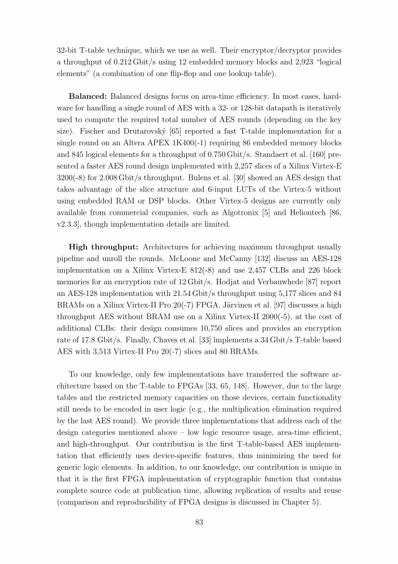
32-bit T-table technique, which we use as well. Their encryptor/decryptor provides
a throughput of 0.212 Gbit/s using 12 embedded memory blocks and 2,923 “logical
elements” (a combination of one flip-flop and one lookup table).
Balanced: Balanced designs focus on area-time efficiency. In most cases, hard-
ware for handling a single round of AES with a 32- or 128-bit datapath is iteratively
used to compute the required total number of AES rounds (depending on the key
size). Fischer and Drutarovsky [65] reported a fast T-table implementation for a
single round on an Altera APEX 1K400(-1) requiring 86 embedded memory blocks
and 845 logical elements for a throughput of 0.750 Gbit/s. Standaert et al. [160] pre-
sented a faster AES round design implemented with 2,257 slices of a Xilinx Virtex-E
3200(-8) for 2.008 Gbit/s throughput. Bulens et al. [30] showed an AES design that
takes advantage of the slice structure and 6-input LUTs of the Virtex-5 without
using embedded RAM or DSP blocks. Other Virtex-5 designs are currently only
available from commercial companies, such as Algotronix [5] and Heliontech [86,
v2.3.3], though implementation details are limited.
High throughput: Architectures for achieving maximum throughput usually
pipeline and unroll the rounds. McLoone and McCanny [132] discuss an AES-128
implementation on a Xilinx Virtex-E 812(-8) and use 2,457 CLBs and 226 block
memories for an encryption rate of 12 Gbit/s. Hodjat and Verbauwhede [87] report
an AES-128 implementation with 21.54 Gbit/s throughput using 5,177 slices and 84
BRAMs on a Xilinx Virtex-II Pro 20(-7) FPGA. Jarvinen et al. [97] discusses a high
throughput AES without BRAM use on a Xilinx Virtex-II 2000(-5), at the cost of
additional CLBs: their design consumes 10,750 slices and provides an encryption
rate of 17.8 Gbit/s. Finally, Chaves et al. [33] implements a 34 Gbit/s T-table based
AES with 3,513 Virtex-II Pro 20(-7) slices and 80 BRAMs.
To our knowledge, only few implementations have transferred the software ar-
chitecture based on the T-table to FPGAs [33, 65, 148]. However, due to the large
tables and the restricted memory capacities on those devices, certain functionality
still needs to be encoded in user logic (e.g., the multiplication elimination required
by the last AES round). We provide three implementations that address each of the
design categories mentioned above – low logic resource usage, area-time efficient,
and high-throughput. Our contribution is the first T-table-based AES implemen-
tation that efficiently uses device-specific features, thus minimizing the need for
generic logic elements. In addition, to our knowledge, our contribution is unique in
that it is the first FPGA implementation of cryptographic function that contains
complete source code at publication time, allowing replication of results and reuse
(comparison and reproducibility of FPGA designs is discussed in Chapter 5).
83

4.3 Implementation
Intended for 32-bit architectures, AES can be implemented as a combination of
lookup (T-tables) and XOR operations; Appendix B provides the mathematical
background for this method, as do Daemen and Rijmen [42, s4.2] and Gladman [71].
Now we show how to adapt this software-oriented approach into modern reconfig-
urable hardware devices in order to achieve high throughput for modest amount
of resources. We use dual-ported 36-Kibit BRAMs, which have independent ad-
dress and data buses for the same stored content, and DSP embedded blocks, which
allow implementation of timing- or resource-critical functions, such as arithmetic
operations on integers or Boolean expressions, that would otherwise be considerably
slower or resource demanding if implemented with traditional logic elements.
DSP blocks were introduced in the Virtex-4 family of FPGAs to perform 18×18
bit integer multiplication along with a 48-bit accumulator, though they were lim-
ited to 24-bit bit-wise logic operations. 48-bit bit-wise logic operations were added
in Virtex-5, and can run at up to 550 MHz, the maximum frequency rating of the
device. The internal datapath of the DSP block is 48 bits wide, except for integer
multiplication. The Virtex-5 DSP blocks come in pairs that span the height of five
configurable logic blocks (CLB); additional pairs can be efficiently cascaded using
dedicated paths to adjacent DSP tiles. A single dual-ported 36-Kibit BRAM also
spans the height of five CLBs and matches the height of the pair of DSP blocks,
with a fast datapath between them. Our initial observation was that the 8- to 32-bit
lookup followed by a 32-bit XOR AES operation perfectly matched this architec-
tural alignment. Based on these primitives, we developed the AES32 module that
outputs one 32-bit AES column every clock cycle (as specified by Equation B.1 in
Appendix B). We have designed it such that it allows efficient placement and routing
of components so it can operate at the maximum device frequency of 550 MHz.
4.3.1 AES32 module
We began with the structure shown in Figure 4.1. Since each column requires
all four T-table lookups, together with their last-round T-table counterparts, that
meant needing to fit eight 8-Kibit T-tables in a single 36-Kibit dual-port RAM. For a
simpler implementation we opted against “reversing” the MixColumns operation for
the last round, and searched for a solution that would enable us to fit all tables into
a single BRAM. We realized that our design can use the fact that all T-tables are
byte-wise transpositions of each other, such that cyclical byte shifting the BRAM
output for T-table T0 produces T1, T2 and T3. Thus, in order to use the entire
BRAM, we can store T0 and T2 together with their last round counterparts T ′0 and
T ′2. Using a single byte circular right rotation (a, b, c, d) → (d, a, b, c), T0 becomes
T1, and T2 becomes T3 and the same for the last round T-tables. In hardware, this
84
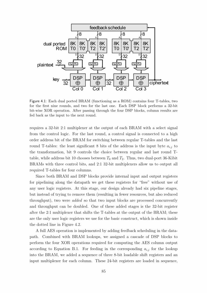
DSP DSP DSP DSP
plaintext
ciphertextkey
8KT0
8KT0'
8KT2
8KT2'
32
3232
32 32 32
8KT0
8KT0'
8KT2
8KT2'
Col 0 Col 1 Col 2 Col 3
32
dual ported ROM
D D D D
8 8 8 8A A A A
feedback schedule
Figure 4.1: Each dual ported BRAM (functioning as a ROM) contains four T-tables, twofor the first nine rounds, and two for the last one. Each DSP block performs a 32-bitbit-wise XOR operation. After passing through the four DSP blocks, column results arefed back as the input to the next round.
requires a 32-bit 2:1 multiplexer at the output of each BRAM with a select signal
from the control logic. For the last round, a control signal is connected to a high
order address bit of the BRAM for switching between regular T-tables and the last
round T-tables: the least significant 8 bits of the address is the input byte ai,j to
the transformation, bit 9 controls the choice between regular and last round T-
table, while address bit 10 chooses between T0 and T2. Thus, two dual-port 36-Kibit
BRAMs with three control bits, and 2:1 32-bit multiplexers allow us to output all
required T-tables for four columns.
Since both BRAM and DSP blocks provide internal input and output registers
for pipelining along the datapath we get these registers for “free” without use of
any user logic registers. At this stage, our design already had six pipeline stages,
but instead of trying to remove them (resulting in fewer resources, but also reduced
throughput), two were added so that two input blocks are processed concurrently
and throughput can be doubled. One of these added stages is the 32-bit register
after the 2:1 multiplexer that shifts the T-tables at the output of the BRAM; these
are the only user logic registers we use for the basic construct, which is shown inside
the dotted line in Figure 4.2.
A full AES operation is implemented by adding feedback scheduling in the data-
path. Combined with BRAM lookups, we assigned a cascade of DSP blocks to
perform the four XOR operations required for computing the AES column output
according to Equation B.1. For feeding in the corresponding ai,j for the lookup
into the BRAM, we added a sequence of three 8-bit loadable shift registers and an
input multiplexer for each column. These 24-bit registers are loaded in sequence,
85
RAM
8
RAM
RAM
RAM
32
32
8
8
8
32
1
2
3
4
plaintext
ciphertext
32
Col 0
32
32
32
Col 1
Col 2
Col 3
keyA:B
A:B
A:B
325
6
7
8
<< 8
1
2
3
4
5
6
7
feedback
Figure 4.2: The AES32 iterative round (without control logic). Plaintext is chosen as theinitial input, then output data is fed back through 8-bit shift registers for a completeAES encryption. Pipeline stage numbers are shown circled. Stage 3 is the output of themultiplexer choosing between non-shifted data or an 8-bit cyclical right-shift or T0 andT2, which are turned into T1 and T3, respectively.
the leftmost (C0) on the first cycle, and the one to its right on the next, and so on.
This construct has eight pipeline stages with the following operations (numbers
in parenthesis correspond to circled numbers in Figure 4.2): lookup (1), where the
8-bit to 32-bit T-table lookup is performed within the BRAM; register (2) is the
BRAM output register; transform (3), where T0 and T2 are optionally shifted into
T1 and T3, respectively; DSP input register (4); and ⊕ (5–8), the XOR operation.
Four processing columns (C[0..3]) are staggered as shown in Figure 4.2. As previously
mentioned, the pipeline stages within the shaded areas are part of the BRAM or
DSP blocks, not user logic flip-flops.
Table 4.1 shows the processing of the first plaintext input, and computation of
86

cyc ptext key fback DSP0 DSP1 DSP2 DSP3 out
1 P[0] K[0] ⊕2 P[1] K[1] ⊕
3 P[2] K[2] ⊕
4 P[3] K[3] ⊕
5 P2[0] K2[0] X0 X0
6 P2[1] K2[1] X1 X1
7 P2[2] K2[2] X2 X2
8 P2[3] K2[3] X3 X3
cyc ptext key fback Col0 Col1 Col2 Col3 out
5 P2[0] K2[0] X0 TLU X0
6 P2[1] K2[1] X1 TOR TLU X1
7 P2[2] K2[2] X2 TS TOR TLU X2
8 P2[3] K2[3] X3 DIR TS TOR TLU X3
9 K0[0] X20 ⊕ DIR TS TOR X20
10 K0[1] X21 ⊕ ⊕ DIR TS X21
12 K0[2] X22 ⊕ ⊕ ⊕ DIR X22
13 K0[3] X23 ⊕ ⊕ ⊕ ⊕ X23
14 K20[0] E0 TLU ⊕ ⊕ ⊕ E0
15 K20[0] E1 TOR TLU ⊕ ⊕ E1
16 K20[0] E2 TS TOR TLU ⊕ E2
17 K20[0] E3 DIR TS TS ⊕ E3
18 K1[0] E20 ⊕ DIR TS TOR E20
19 K2[1] E21 ⊕ ⊕ DIR TS E21
20 K3[2] E22 ⊕ ⊕ ⊕ DIR E22
Table 4.1: The top part of the table shows the input of plaintext and the operation ofthe DSPs. DSP0 performs a 32-bit XOR on the input P[0..3] and the main key K[0..3]; theoutput (X[0..3]) propagates unchanged through the other DSP blocks. The bottom tableshows X[0..3] being processed for an AES round. The stages are: table lookup (TLU); tableoutput register (TOR); T-table shift (TS); DSP input register (DIR); and, DSP XOR ⊕.The outputs E[0..3] are used as input to the next round, and so on. The gray inputs andoutputs show the second input block that is possible. (The overlap between the two partsis shown by dotted lines).
the first round. The input is operated on as four 32-bit words, each XOR’d with
the main key by DSP0. The output of the operation, X[0..3], propagates through
the other DSPs without change (by resetting their A:B inputs to ‘0’). Each of these
32-bit outputs is then used as feedback to the columns: X0 for the feedback registers
of Col0, X1 for Col1, and so on. The Verilog code for the exact feedback network
is shown in Figure 4.3, and Equation B.1 defines the order. E[0..3] are the outputs
of the first round, which are fed back for the second round, and so on. The grayed
inputs and outputs in Table 4.1 show the second independent 128-bit input that
87

module aes32_dsp_8p_fb_con (
input wire CLK,input wire [31:00] DIN, // feedback inputinput wire [01:00] CTRL, // column controloutput wire [31:00] DOUT);
reg [23:00] c0,c1,c2,c3;
wire [07:00] c0_out, c0_1, c0_2;wire [07:00] c1_out, c1_1, c1_2;wire [07:00] c2_out, c2_1, c2_2;wire [07:00] c3_out, c3_1, c3_2;
assign DOUT = c0_out, c1_out, c2_out, c3_out;
assign c0_out = (CTRL[1:0] == 2’b00) ? DIN[31:24] : c0[07:00];assign c0_1 = (CTRL[1:0] == 2’b00) ? DIN[07:00] : c0[15:08];assign c0_2 = (CTRL[1:0] == 2’b00) ? DIN[15:08] : c0[23:16];
assign c1_out = (CTRL[1:0] == 2’b01) ? DIN[23:16] : c1[07:00];assign c1_1 = (CTRL[1:0] == 2’b01) ? DIN[31:24] : c1[15:08];assign c1_2 = (CTRL[1:0] == 2’b01) ? DIN[07:00] : c1[23:16];
assign c2_out = (CTRL[1:0] == 2’b10) ? DIN[15:08] : c2[07:00];assign c2_1 = (CTRL[1:0] == 2’b10) ? DIN[23:16] : c2[15:08];assign c2_2 = (CTRL[1:0] == 2’b10) ? DIN[31:24] : c2[23:16];
assign c3_out = (CTRL[1:0] == 2’b11) ? DIN[07:00] : c3[07:00];assign c3_1 = (CTRL[1:0] == 2’b11) ? DIN[15:08] : c3[15:08];assign c3_2 = (CTRL[1:0] == 2’b11) ? DIN[23:16] : c3[23:16];
always @(posedge CLK) beginc0 <= DIN[23:16], c0_2, c0_1;c1 <= DIN[15:08], c1_2, c1_1;c2 <= DIN[07:00], c2_2, c2_1;c3 <= DIN[31:24], c3_2, c3_1;
end
endmodule
Figure 4.3: Verilog code for the AES32 feedback network.
can be used with the same circuit; that is, for each column entry there is another
operation performed for the second input.
Finally, we also tried a different datapath using the same basic structure, but
instead of feeding the output of each DSP to the one on its right, the data is fed back
into the same DSP, and then XOR’d with the new T-table input. This, however,
requires the input of a key to each DSP block, extra control logic, dynamic change
of DSP operating modes, and a 32-bit 4:1 mux to choose between the output of each
DSP for the feedback schedule. All those introduced additional delays when routed,
so performance was poorer than the alternative previously described.
4.3.2 AES128 and AES128U modules
AES32 can be replicated four times for a 128-bit datapath: for each instance, the
feedback network is replaced with 8-, 16-, and 24-bit registers for columns 1, 2 and 3,
respectively. The first of four instances is shown in Figure 4.4: one byte is fed back
to the same instance while three bytes are distributed to the other three instances;
Verilog code for the feedback schedule shown in Figure 4.5. The latency of this
88
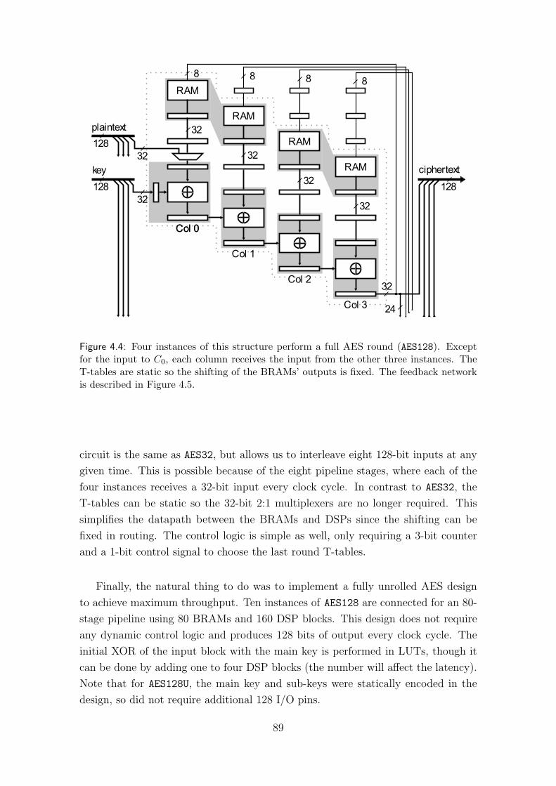
RAM
8
RAM
RAM
RAM
32
8 8 8
24
plaintext
32
key
32
32
32
32
ciphertext
Col 0
Col 1
Col 2
Col 3
128128
32128
Col 0
Figure 4.4: Four instances of this structure perform a full AES round (AES128). Exceptfor the input to C0, each column receives the input from the other three instances. TheT-tables are static so the shifting of the BRAMs’ outputs is fixed. The feedback networkis described in Figure 4.5.
circuit is the same as AES32, but allows us to interleave eight 128-bit inputs at any
given time. This is possible because of the eight pipeline stages, where each of the
four instances receives a 32-bit input every clock cycle. In contrast to AES32, the
T-tables can be static so the 32-bit 2:1 multiplexers are no longer required. This
simplifies the datapath between the BRAMs and DSPs since the shifting can be
fixed in routing. The control logic is simple as well, only requiring a 3-bit counter
and a 1-bit control signal to choose the last round T-tables.
Finally, the natural thing to do was to implement a fully unrolled AES design
to achieve maximum throughput. Ten instances of AES128 are connected for an 80-
stage pipeline using 80 BRAMs and 160 DSP blocks. This design does not require
any dynamic control logic and produces 128 bits of output every clock cycle. The
initial XOR of the input block with the main key is performed in LUTs, though it
can be done by adding one to four DSP blocks (the number will affect the latency).
Note that for AES128U, the main key and sub-keys were statically encoded in the
design, so did not require additional 128 I/O pins.
89
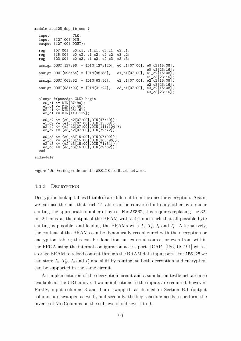
module aes128_dsp_fb_con (
input CLK,input [127:00] DIN,output [127:00] DOUT);
reg [07:00] e0_c1, e1_c1, e2_c1, e3_c1;reg [15:00] e0_c2, e1_c2, e2_c2, e3_c2;reg [23:00] e0_c3, e1_c3, e2_c3, e3_c3;
assign DOUT[127:96] = DIN[127:120], e0_c1[07:00], e0_c2[15:08],e0_c3[23:16];
assign DOUT[095:64] = DIN[95:88], e1_c1[07:00], e1_c2[15:08],e1_c3[23:16];
assign DOUT[063:32] = DIN[63:56], e2_c1[07:00], e2_c2[15:08],e2_c3[23:16];
assign DOUT[031:00] = DIN[31:24], e3_c1[07:00], e3_c2[15:08],e3_c3[23:16];
always @(posedge CLK) begine0_c1 <= DIN[87:80];e1_c1 <= DIN[55:48];e2_c1 <= DIN[23:16];e3_c1 <= DIN[119:112];
e0_c2 <= e0_c2[07:00],DIN[47:40];e1_c2 <= e1_c2[07:00],DIN[15:08];e2_c2 <= e2_c2[07:00],DIN[111:104];e3_c2 <= e3_c2[07:00],DIN[79:72];
e0_c3 <= e0_c3[15:00],DIN[07:00];e1_c3 <= e1_c3[15:00],DIN[103:96];e2_c3 <= e2_c3[15:00],DIN[71:64];e3_c3 <= e3_c3[15:00],DIN[39:32];
end
endmodule
Figure 4.5: Verilog code for the AES128 feedback network.
4.3.3 Decryption
Decryption lookup tables (I-tables) are different from the ones for encryption. Again,
we can use the fact that each T-table can be converted into any other by circular
shifting the appropriate number of bytes. For AES32, this requires replacing the 32-
bit 2:1 mux at the output of the BRAM with a 4:1 mux such that all possible byte
shifting is possible, and loading the BRAMs with Ti, T ′i , Ii and I ′i. Alternatively,
the content of the BRAMs can be dynamically reconfigured with the decryption or
encryption tables; this can be done from an external source, or even from within
the FPGA using the internal configuration access port (ICAP) [186, UG191] with a
storage BRAM to reload content through the BRAM data input port. For AES128 we
can store T0, T ′0′ , I0 and I ′0 and shift by routing, so both decryption and encryption
can be supported in the same circuit.
An implementation of the decryption circuit and a simulation testbench are also
available at the URL above. Two modifications to the inputs are required, however.
Firstly, input columns 3 and 1 are swapped, as defined in Section B.1 (output
columns are swapped as well), and secondly, the key schedule needs to perform the
inverse of MixColumns on the subkeys of subkeys 1 to 9.
90

DIN
ADDR
WE
DOUT
DIN
ADDR
WE
DOUT
controllogic
instructions
key output32
8
8
12
32
10 A
B
Figure 4.6: Block diagram of key expansion implementation. The S-boxes, round constantsand 32-bit subkeys are stored in the dual-port BRAM connected to an 8-bit datapath.Unused memory in the BRAM is used to encode 32-bit instructions for the state machine.
4.3.4 Key expansion
A dual-ported BRAM stores the expanded 32-bit subkeys (44 words for AES-128),
the round constants (10 32 bit values) and S-box entries with 8 bits each. A block
diagram of the implementation is shown in Figure 4.6: port A of the BRAM is 32
bits wide and feeds the subkeys to the AES module, while port B is configured for 8-
bit data I/O. With an 8-bit multiplexer, register and XOR connected to port B data
output, this circuit can compute the full key expansion (described in Section B.2).
The key expansion circuit requires a complex state machine whose control logic
is likely to become the critical path, so we encode it in the spare storage of a BRAM.
Recall that the BRAM provides 36-Kibits of memory of which 1,408 to 1,920 bits
are required for subkeys (for AES-128 and AES-256, respectively), 2,048 bits for
S-box entries and 80 bits for round constants, so the BRAM is not completely full.
Therefore, to save user logic resources, all memory addresses and control logic signals
are encoded as 32-bit instructions and stored in the unused part of the BRAM. This
method also ensures constant and uniform signal propagation for all control signals
since they do not need to be generated by combinatorial logic.
4.4 Results
Our designs target a Virtex-5 SX50T4 (FF1136 package) FPGA at its fastest speed
grade (-3) using the ISE 10.1i.03 implementation flow with Xilinx Synthesis Tech-
nology (XST). We used Mentor Graphics ModelSim 6.2g for both behavioral and
post place-and-route simulation, under nominal conditions for core voltage (0.95 V)
4We chose the SX50T because it is the smallest that can accommodate all three variants of ourdesign; this makes our reporting consistent. Note that while the SX35T has enough logic resources,it has insufficient number of I/Os.
91

designdec/ datapath/ resources f perf.key streams slices LUT FF BRAM DSP MHz Gbit/s
AES32 / 32/2 107 320 257 2 4 550 1.67AES128 / 128/8 259 338 624 8 16 550 6.7AES128U •/ 128/80 321 738 1,031 80 160 413 52.8Algotronix / 32/2 161 n/a n/a 2 0 250 0.8Helion /• 128/1 349 n/a n/a 0 0 350 4.07Bulens et al. /• 128/1 400 n/a n/a 0 0 350 4.1
Table 4.2: Our results, with other related academic and commercial implementations onVirtex-5 devices. Decryption (Dec.) and Key expansion (Key) are included when denotedby •, by otherwise. For AES32 and AES128 implementations, decryption can be achievedby adding 32-bit muxes in the datapath between BRAM and DSP. Other Virtex-5 AESimplementations are listed for reference, and we do not make a direct comparison to them;see Chapter 5 for a discussion.
and temperature (85 ), using minimum delay data (netgen option -s min). We
did not verify the designs on an actual device, except for the CMAC implementation
described in Section 4.5.1.
XFLOW [188, ch25] was used as an implementation wrapper for the ISE flow5:
we used xst verilog.opt for synthesis and high effort.opt as the basis for the
implementation, and customizing them for best results (i.e., effort levels, optimiza-
tion techniques, etc.) We used “multi-pass place-and-route” options -t 1 (starting
seed number) and -n 100 (the number of seeds to try), and raised the PAR effort to
-o high, such that each design was implemented using a hundred PAR seeds6, and
the best result is reported here7. The only constraint given to the tools was for the
minimum clock period (NET CLK PERIOD = 1.818 ns, for example). (That is, no
other logical function was implemented together with the respective AES module,
and no restriction on I/O and resources placement was made.)
Results are summarized in Table 4.2. AES32, as shown in Figure 4.2, passed
timing (post place-and-route) for a frequency of 550 MHz, the maximum frequency
rating of the device. The design requires the following resources: 257 flip-flops, 96
(8·3·4) for the input shift registers plus 128 (4·32) for the pipeline stages in between
the BRAMs and DSPs, with the rest used for control logic; 320 lookup tables,
mostly functioning as multiplexers; and finally, two 36-Kibit dual-port BRAM (32-
Kibit used in each) and four DSP48E blocks. Throughput is calculated as follows:
given that there are 84 processing cycles (80 for round operations and 4 for input)
5XFLOW is an ISE tool; a typical command is: xflow -p xc5vsx50tff1136-3 -synth xst-verilog.opt -implement high effort.opt -config bitgen.opt <design>.v where the op-tion files are pre-defined, but can be edited for custom settings.6These are called “cost tables” by Xilinx, and they introduce variability to the PAR process sodesigns meet their timing goals; we discuss these in Chapter 5.7Results that exceeded the maximum frequency rating of the FPGA (550 MHz) were capped tothat frequency; in some cases, the best results are outliers, and we will discuss this at length inChapter 5.
92

Keyexpansion
Resources f Cyclesslices LUT FF BRAM DSPs (MHz)
AES-12837 55 41 1 0 550
524AES-192 628AES-256 732
Table 4.3: Implementation results for the AES key expansion design. Most state machinecontrol logic has been encoded into a BRAM to save logic resources.
operating at 550 MHz and 256 bits of state in the pipeline stages, 550 ·106 ·256/84 =
1.67 Gbit/s of throughput is achieved. This assumes that the pipeline stages are
always full, meaning that the module is processing two 128-bit inputs at any given
time; if only one input is processed, throughput is halved. As mentioned, the eight
stages allow interleaving of two inputs, though the designer can remove stages in
order to reduce resources (the pipeline registers between the BRAMs and DSPs
consume the most logic resources; others are part of the embedded primitive). This,
of course, may reduce performance, so there is a trade-off that needs to be evaluated
according to target performance.
The maximum operating frequency for AES128 is also 550 MHz, which requires
624 flip-flops, 338 lookup tables, 8 36-Kibit BRAMs (32-Kibit used in each), and
16 DSP48E blocks. The latency of 84 clock cycles is the same as the previous
design, though now we maintain state of 128 · 8 = 1024 bits for a throughput of
550 ·106 ·8 ·128/84 = 6.7 Gbit/s when processing eight input blocks. As with AES32,
pipeline stages can be removed to minimize the use of logic resources if they are
required for other functions at the expense of throughput.
Finally, the AES128U implementation produces 128 bits of output every clock
cycle once the initial latency is complete. We have experimented with eliminating the
pipeline stage between the BRAM and DSP to see if it adversely affects performance;
this will save us 5,120 registers. We found that the performance degradation is low,
with the added benefit of having an initial latency of only 70 clock cycles instead
of 80 (in principle, this could also be done also for AES128, but then only seven
streams can be processed concurrently). The resulting throughput is 413 ·106 ·128 =
52.8 Gbit/s. This design operates at a maximum frequency of over 413 MHz and uses
1,031 flip-flops, 738 lookup tables, 80 36-Kibit BRAMs (only 16-Kibit in each for
either encryption or decryption, or 32-Kibit for both), and 160 DSP48E blocks. The
design only uses 3.2% and 2.3% of flip-flops and LUTs of the SX50T, respectively,
though 60% of BRAMs and 55% of DSP48Es are used.
The reported results are based on the assumption that the set of subkeys are
externally provided through the I/O (AES32 and AES128), or are statically encoded
in the design (AES128U). Where all subkeys are generated internally, these modules
can be augmented with a key expansion stage pre-computing all subkeys and stor-
93

EK EK EK
M1 M2 Mn
K or K
MACC1 C2
1 2
EK
Mn-1
Cn-1
Figure 4.7: CMAC mode of operation. The choice of K1 or K2 is determined by if Mn isa complete block or not.
ing them in a dedicated BRAM. As discussed in Section 4.3.4, the key expansion
circuit is optimized for a small footprint and allows operation at the maximum de-
vice frequency of 550 MHz. The complexity of the state machine, which is the most
expensive part in terms of logic, is mostly hidden within the encoded 32-bit instruc-
tions stored in the BRAM. Hence, since only a small stub of the state machine is
implemented in logic, the overall resource consumption of the full key expansion is
only 1 BRAM, 55 LUTs and 41 flip-flops. Table 4.3 summarizes these results, with
support for key sizes of 128, 192 and 256 bits.
4.5 Extensions
We have discussed three pipelined architectures for AES that support simultaneous
encryption of 2, 8, and 80 128-bit input blocks in electronic codebook (ECB) mode.
We now consider other block-cipher modes of operation that use AES encryption as
a building block and fit well into our design architecture.
4.5.1 Message authentication: CMAC
Besides encryption, the CBC mode can be used to produce a message authentication
code (CBC-MAC) by simply discarding all ciphertext blocks except the last one.
CBC-MAC is known to be vulnerable to message extension attacks where the length
of the message is not fixed or checked. To deal with these shortcomings, NIST has
defined the CMAC mode [139, 800-38B], where a derivative of the key is applied
before the last AES invocation; the basic CMAC construct is shown in Figure 4.7.
CMAC’s last AES invocation is unique in that it requires an extra XOR of
one of two keys, K1 or K2, with Mn ⊕ Cn−1. If the entire message divides evenly
into n blocks, then K1 is used, otherwise Mn is appended with a predetermined
suffix to create a complete block, and K2 is used. Although we do not consider
94

RAM
8
RAM
RAM
RAM
32
32
8
8
8
32
plaintext
ciphertext
32
Col 0
32
32
32
Col 1
Col 2
Col 3
key A:B
A:B
A:B
32
32
Figure 4.8: Additions made to AES32 for CMAC operation. Three 32-bit registers areadded in order to keep the output in between AES invocations and are XOR’d with thenext plaintext block and initial key of the first round. The input “key” is expected toreceive all AES subkeys and K1/K2 at the appropriate time; their generation and themessage block padding are not part of the design.
it in the implementation, we provide the generation description of K1 and K2 for
completeness:
K1 = MSB(L) ? (L 1) ⊕ R : (L 1)
K2 = MSB(K1) ? (K1 1) ⊕ R : (K1 1),
where L = Ek(0128) (an AES encryption of the zero vector under the main key), and
R = 012010000111; MSB indicates “most significant bit”.
Our implementation is shown in Figure 4.8. The inputs to the design are plain-
text blocks M1...n, keys, and feedback, which is the output of column three. As with
AES32, the feedback is used as input to the four columns between round iterations,
though now it is also fed back as the input for subsequent AES invocations. First,
plaintext M1 is sent through the two multiplexers and XOR’d with the main AES
key; the result is propagated through the rest of the DSP blocks while their A : B
inputs are held at reset. The output is then fed back to the top input registers and
ten AES rounds are performed using the round keys as described in Section 4.3.1.
95
The ciphertext output C1 is then XOR’d with M2 before another invocation of AES
occurs. Prior to the last invocation of AES an extra feedback cycle is performed for
the K1 or K2 XOR operation.
Notice that in Figure 4.8 the delayed feedback is used as an input to two 32-bit
multiplexers. The reason for this is that the feedback needs to be XOR’d with both
the key and the plaintext, as in the last AES invocation, ((Cn−1⊕Mn)⊕K1/2)⊕KAES.
In addition to the input muxes, three 32-bit registers keep the state of the output
feedback as the pipeline stages are being cleared.
As before, two independent streams can be interleaved. If the same input is used
for both streams, a MAC and CBC/ECB output can be generated concurrently. If
decryption is added to the design with the required additional shifts, as discussed in
Section 4.3.3, then decryption and MAC-generation can be performed in the same
run. The only difference is that for encryption and decryption K1 and K2 will need
to be set to zero, and intermediate values of Ci are output, while they are not when
producing a MAC. (Remember that for security, MAC and ciphertext should not be
produced using the same key.)
We have optimized the implementation for maximal use of the pipeline stages.
First, the initial XOR of the key and plaintext message is performed, and the first
output for feedback appears after six cycles (two for input registers and four to
propagate through the DSP48E blocks). Then, 80 additional cycles complete the
first AES invocation. KAES ⊕ (Cn−1 ⊕Mn) requires 16 cycles (eight for each XOR)
with two additional pipeline cycles at the end. Thus, for N input blocks (if the
message is empty then N = 1), a MAC is produced every
(6 + 80) + (N − 2)(16 + 80) + (16 + 8 + 80) + 2 = 96 ·N
cycles. For example, for N = 4 a MAC is computed every 384 cycles.
The design achieves a maximum frequency of 511 MHz (under the the same im-
plementation conditions as the other variants) and requires 357 registers, 457 LUTs
(in 205 slices) that include input registers for data and keys; as before, the design
uses two 36 KB dual-ported BRAMs and four DSP48Es, and was simulated at both
the behavioral and post place-and-route stages. The throughput is dependent on N
and with 511 MHz operation comes to 511·106 ·256/96/N , so for N = 1, 1.362 Gbit/s
for two interleaved streams.
4.5.2 CTR and CCM modes
Our modules can be used with other modes of operation. Counter mode [139, 800-
38A] requires a fast counter of up to 128 bits in width. The carry propagation delay
of such a wide counter implemented in user logic will limit performance, so a cas-
cade of DSP blocks is used instead (shown in Figure 4.9). Virtex-5 devices support
96

AES
incrementcarry
carry
324848
128resetkey
DIN
DOUT
reset
reset
reset
INIT1
INIT2
INIT3
Figure 4.9: CTR mode circuit that is compatible with all three AES modules. Threeadjacent DSP blocks build a 128-bit adder to increment an integer counter.
Design Resources Perf.slices LUT FF RAM (MHz)
AES32 XOR 212 (1.98) 448 (1.4) 554 (2.15) 2 550AES128 XOR 624 (2.40) 850 (2.51) 1,776 (2.84) 8 550AES128U XOR 3,775 (11.76) 5,121 (6.94) 10,652 (10.33) 80 440
Table 4.4: Results when DSPs are replaced with logic (on an SX50T) under the sameconditions as for the results reported in Table 4.2. Numbers in parenthesis indicate increasemultiplier from DSP-based design.
the generation of wide, parallel adders using dedicated carry signals CARRYCAS-
COUT and CARRYCASCIN that can be used to ripple carries through adjacent
DSP blocks. For a 128-bit counter, three adjacent DSP blocks in accumulation
mode are connected – each can add operands of up to 48 bits. Since carry prop-
agation between DSPs occurs on clock edges, alignment using output registers is
required. An implementation of this counter operates at 550 MHz.
In a similar way that CMAC was implemented, the counter with CBC-MAC
(CCM) authenticated encryption mode [139, 800-38C] can be implemented. This
requires two AES operations to be performed in parallel – one for encrypting or
decrypting data and another for creating or verifying a MAC. Thus, with an ad-
ditional encryption counter, it is possible to adapt our modules to provide CCM
authenticated encryption for 1, 4, or 40 individual streams of data.
4.5.3 Replacing DSPs with CLBs
Our design can be modified so that it can be implemented on other architectures. To
do this, the DSP 32-bit bit-wise XOR and internal pipeline registers were replaced
with traditional user logic (AES32 XOR, AES128 XOR, AES128U XOR). The results are
shown in Table 4.4 (simulation and implementation conditions remain the same, and
97

the source code is available at the above URL). Performance is comparable8 to the
DSP versions due to the pipelined nature of the designs and also because the place
and route process is less constrained by not needing to meet the timing imposed by
DSP placement. As expected, flip-flop and LUT usage has increased.
We maintain that under our assumed constraint of scarcity of logic resources,
for which our original designs was meant for, any increase may be a disadvantage.
While the logic-only design is more like the previous implementations discussed in
Section 4.2, it also makes our designs more portable. We also recognize that the
DSPs themselves are underutilized, as they can perform much more than wide bit-
wise operations (we do not use the multiplier, for example). But again, we assumed
that these DSPs were not used in the first place. Any FPGA resource that is not
used is a loss because the system developer paid for it either way; we simply provide
fast AES designs that may fit these unused resources.
4.6 Conclusions
We have presented new ways for performing AES operations at high throughput
using on-chip RAM and DSP blocks with comparatively low use of traditional user
logic such as flip-flops and lookup tables. We have also described and implemented
the CMAC and CTR modes of operation, and a compact key expansion function
for pre-computing keys. The source code for all the three AES variants and CMAC
mode is publicly available so that they can be used in further research, and provide
readers with the ability to reproduce our reported results.
While our results appear to be good, they are admittedly misleading, as the
throughput we – and perhaps other researchers – report will not be achieved in
practice when the modules are used as part of a bigger system. There are several
reasons for this, all discussed in the next chapter.
8As we shall see in Chapter 5, AES128U XOR may perform noticeably better than AES128U DSP ifthe clock frequency constraint is set to a higher value. The upper bound for this constraint isdetermined by the tools, which warn if it is set to an unachievable value. For consistency, bothversions were executed with the same constraint of 435 MHz.
98

Chapter 5
The meaning and reproducibility
of FPGA results
In this chapter, we discuss the significant performance variability of FPGA designs,
and question the reproducibility of, and comparability with, other published results.
Throughput, a popular measure of performance, is a function of many factors, in-
cluding not only the HDL design itself, but also tool versions, implementation op-
tions, device architecture, and in particular, how connected modules constrain the
design. Throughput alone neither specifies the optimization goal of every design,
nor is such a single figure of merit a fair measure with which to compare, even where
it was the optimization goal.
The peer-review process expects that new contributions be compared with pre-
viously published work. But doing so in a fair, meaningful and reproducible way
is challenging. We first describe a few simple and easy to reproduce experiments
that demonstrate the problem: the substantial variability of commonly reported
and compared figures of merit, such as throughput or maximum clock frequency,
under seemingly trivial changes to the build environment (Section 5.1). We then
discuss what we consider to be good practice in reporting and comparing the perfor-
mance of FPGA implementations and practices that we believe should be avoided,
or at least treated with caution (Section 5.2). We hope that this discussion will
help both authors and reviewers of future FPGA implementations avoid some of the
most common pitfalls when comparing results. As a research community, we have to
recognize the importance of reproducibility as seriously as any other experimental
discipline. See Section 5.4 for some related work.
In spite of our other recommendations on how to report performance results,
we conclude that there ultimately is no substitute for releasing the full source code
and build environment of an implementation, so that other researchers can exactly
reproduce measurements in practice, and rerun them on newer platforms, where
applicable. If we care about reproducible research, we have to treat the source
99

files of the implementation as the primary scholarly contribution, and can count
explanatory papers and measurement results only as a form of advertisement for
the former.
5.1 Demonstration experiments
Since AES implementation has been a particularly active research area in recent
years, we use the AES128 implementation from Chapter 4 as a demonstration ex-
ample. As far as we are aware, of all the many academic publications describing an
FPGA implementation of a cryptographic function to date, Drimer et al. [56] was
the first, and is so far the only, publication to provide a URL in the body of the text
for downloading both the source HDL and instructions for reproducing the reported
results1. Source code and test benches for simulation and reimplementation of all
experiments in this chapter are available at:
http://www.cl.cam.ac.uk/~sd410/aes2/ (version 1.0)
We run each example design with 100 different place-and-route (PAR) seeds2,
thus providing different weights for constraints, placement starting points and other
factors that affect timing (more in text box on the next page). PAR seeds are used
by developers to help them make their designs achieve specific target frequency
performance, but here we use them to illustrate how small perturbations in the
PAR start conditions (also leading to routing changes) affect the performance of
a design, especially when it is “unconstrained”, by which we mean that there are
no other circuit elements competing for available resources. (We do constrain the
design by setting a performance target for the clock frequency; note that different
targets produce varying allocation of logic resources.) We report each run’s “best
case achievable” frequency given by the timing analyzer, and ignore routes from
I/Os for timing.
5.1.1 Application context
Cryptographic primitives, such as AES, are usually part of a bigger design, and are
rarely used in isolation. Most FPGA implementations in the literature, however,
are reported as unconstrained, stand-alone modules. They lack the context of the
application in which they will be used. If a small module occupies a large device,
the tools have more freedom to use the shortest routes available, and so perform
1The closest contender was a 2002 technical report by Weaver and Wawrzynek [182] who providedAES code, though we found this no longer available.2Xilinx calls these “cost tables” that can be activated by adding the -t 1 and -n 100 switcheswhen executing par. Our experiments show that results for each cost table are consistent so thatreproducibility is possible if the same source code is implemented with the same settings.
100

better. As more logic needs to be packed into a given resource area, available routing
and resource options become scarce, making it difficult to achieve the same perfor-
mance. The tools are then forced to use less efficient routes, increasing the delay
on the critical path. Therefore, “maximum frequency” results from unconstrained
implementations are useful in a limited way. They indicate the maximum frequency
a module can achieve under the most favorable circumstances, not the one it will
achieve in practice, when embedded into a real application.
Now we demonstrate how implementation conditions affect both the “maximum
frequency” a design can achieve, and the significant variation of results from dif-
ferent seed runs. We have implemented AES128 in two ways. The first is uncon-
strained (same as for the results reported in Chapter 4), and the second is where
four AES128 instances are chained (Figure 5.1). Both designs were implemented for
a Virtex-5 LX110-3 and SX50T-3 FPGAs. The SX50T has 288 DSP blocks and
132 BRAMs [186, DS100, t1] so both designs fit easily. The LX110, however, has
only 64 DSPs and 128 BRAMs, so the DSPs become a scarce resource depriving the
place-and-route algorithm from flexibility otherwise available for a single-instance
Cost tables? The exact ways in which synthesis and PAR algorithms workin commercial tools are often opaque to the user; “cost tables” are a numericabstraction of various placement tweaks the tools make when the engineer tellsthem to try harder to achieve better performance. It seems that this techniquein the Xilinx tools originated from NeoCADa (who were later bought by Xilinx),and while today’s guides are not forthcoming with informationb, older guideswere slightly more revealing. A user guidec for version 3.1i of the Xilinx tools(circa 1999) elaborates and specifies that
[O]n average, design speed from an arbitrary multiple pass place androute will vary plus or minus 5% to 10% from the median design speedacross all cost tables. About 1/3 of the cost tables will result in speedswithin 5% of the median, 1/3 in the 5% to 10% range, and 1/3 in the10% to 15% range. When comparing performance from the absoluteworst cost table to the absolute best, a spread of 25% to 30% is possible.
Kilts [107, s16.9] dedicates a few pages to discuss “placement seeds”, endingwith an interesting observation: if one relies on them to meet timing goals, thenmargins are already too tight, as any slight change to the design may cause itto fail. Thus, this technique should only be used when the design is finalized,and even then, with caution.
ahttp://www.deepchip.com/posts/0178.htmlbSee “note” on page 369, “Development system reference guide 9.2i”,http://www.xilinx.com/itp/xilinx92/books/docs/dev/dev.pdfcSee page 3-36 in “Design manager/flow engine guide”,http://www.xilinx.com/itp/xilinx4/pdf/docs/dmf/dmf.pdf
101

AESkey
plaintext128 AES AES AES
16x DSP48E 16x DSP48E 16x DSP48E 16x DSP48E
Figure 5.1: Four instances of AES128 are chained to show how results may vary when asingle instance is part of a larger design. (Note that this design was not tested for correctoperation, as it just serves to demonstrate variability.)
implementation. Implementation conditions and settings are identical to the ones
detailed in Section 4.4.
We can make several observations from the results (Figure 5.2). The single
instance implementation on an LX110 (1) varies by over 200 MHz, more than a third
of the entire range (zero to 550 MHz). The SX50T implementation (3), on the other
hand, provides more confidence in a single figure of performance because results
are more concentrated. The reason for this is that DSPs are more abundant and
concentrated in the SX devices than they are in the LX’s. The difference between
the single instance implementation on the two devices (1 and 3) clearly show that the
choice of a family member within a class of FPGAs can significantly affect results.
When designs are constrained (2 and 4), they perform noticeably worse, but results
are more concentrated, providing more confidence in a single figure of performance;
we can see that the most constrained design (2) has the least variance. Given these
results, which is the most accurate single number that best reflects the effective
performance of the design?
The results do not necessarily mean that the design or the development tools
are “bad”, but rather that “results may vary” – that is, the “maximum frequency”
reported for a single PAR run alone is not a good predictor of how the design will
perform under various constraints or conditions. Practically achievable performance
depends on many factors not represented in an unconstrained implementation: tool
versions, I/O placement constraints, etc. In addition to PAR seeds, there are also
“cost tables” for the map process (where resources are allocated for the design ac-
cording to the target performance that is specified).
Even if this particular example design is not representative of all designs, it
serves to show the point. Such dramatic decreases in performance can probably be
avoided if designs are constructed more carefully, but the question remains how to
demonstrate experimentally that predictable performance was achieved. Reporting
the utilization percentage of the device’s resources (or ones available within a par-
tition), and running the design on several device sizes and types of the same family
could provide useful information.
102
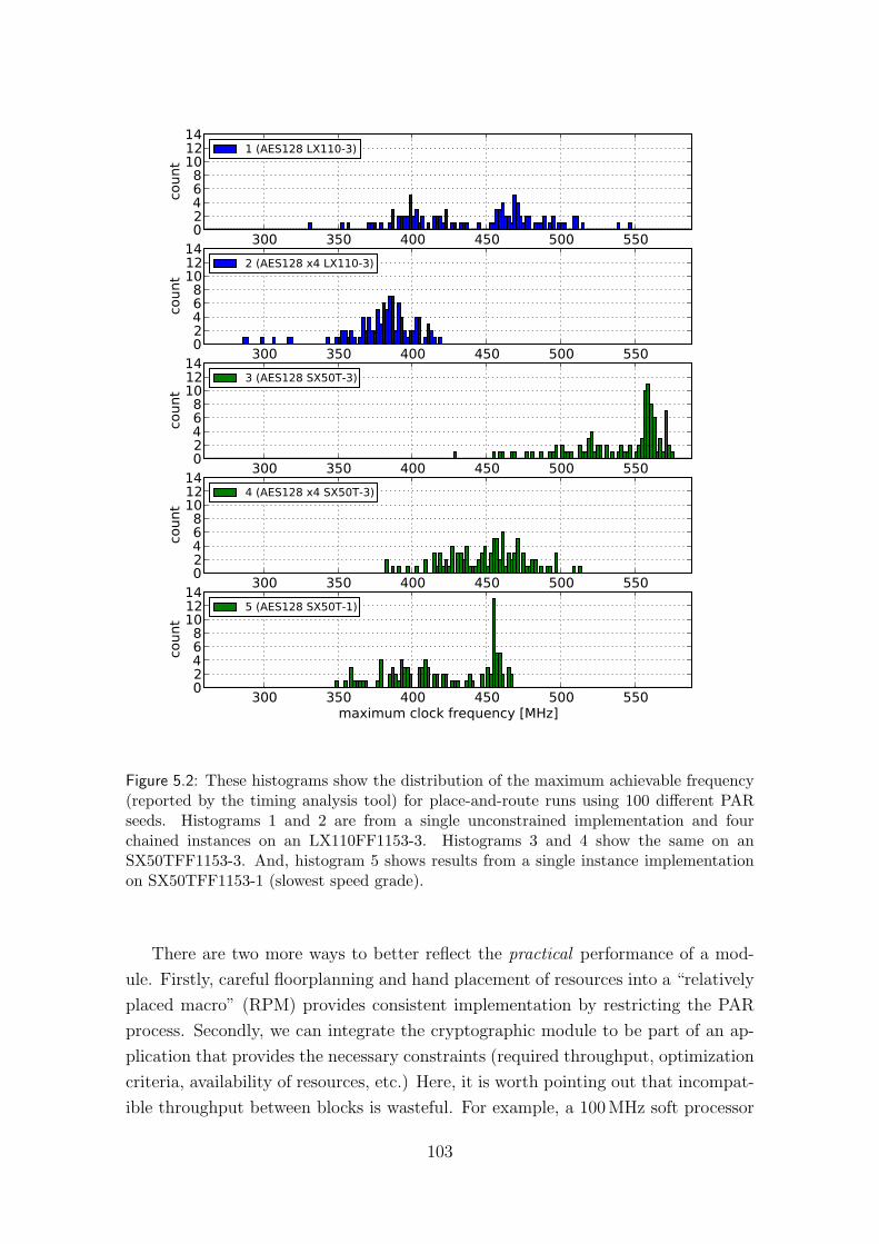
300 350 400 450 500 55002468
101214
count
1 (AES128 LX110-3)
300 350 400 450 500 55002468
101214
count
2 (AES128 x4 LX110-3)
300 350 400 450 500 55002468
101214
count
3 (AES128 SX50T-3)
300 350 400 450 500 55002468
101214
count
4 (AES128 x4 SX50T-3)
300 350 400 450 500 550maximum clock frequency [MHz]
02468
101214
count
5 (AES128 SX50T-1)
Figure 5.2: These histograms show the distribution of the maximum achievable frequency(reported by the timing analysis tool) for place-and-route runs using 100 different PARseeds. Histograms 1 and 2 are from a single unconstrained implementation and fourchained instances on an LX110FF1153-3. Histograms 3 and 4 show the same on anSX50TFF1153-3. And, histogram 5 shows results from a single instance implementationon SX50TFF1153-1 (slowest speed grade).
There are two more ways to better reflect the practical performance of a mod-
ule. Firstly, careful floorplanning and hand placement of resources into a “relatively
placed macro” (RPM) provides consistent implementation by restricting the PAR
process. Secondly, we can integrate the cryptographic module to be part of an ap-
plication that provides the necessary constraints (required throughput, optimization
criteria, availability of resources, etc.) Here, it is worth pointing out that incompat-
ible throughput between blocks is wasteful. For example, a 100 MHz soft processor
103

300 350 400 450 500 55002468
101214
count
AES32_DSP
300 350 400 450 500 55002468
101214
count
AES128_DSP
300 350 400 450 500 550maximum clock frequency [MHz]
02468
101214
count
AES128U_DSP
Figure 5.3: 100 cost table runs for AES32, AES128, and AES128U with DSPs performing the32-bit XORs.
limiting a high-performance 500 MHz AES module it is attached to usually means
that the AES module is wasting resources, as performance correlates to resource-use
(pipelining, unrolling, etc.), and dynamic power to frequency. In this case, a better
choice would have been to optimize the AES module for 100 MHz operation so it
consumes fewer resources, or have different clock domains for the two modules. In
real-world applications, decreasing resource use is crucial as it could reduce costs
by requiring, for example, a smaller FPGA, which may also decrease circuit board
space and static power consumption.
The “speed grade” of a device indicates the maximum frequency rating of par-
ticular functions inside the FPGA. For example, Virtex-5 currently has three speed
grades: -1 (slowest), -2, and -3 (fastest). Not reporting the target speed grade can
lead to misinterpretation of results. To illustrate the importance of this, we ran
AES128 for a -3 and -1 SX50T; this is shown in histograms 3 and 5 of Figure 5.2.
Figures 5.3 and 5.4 show the results for each of the three implementations re-
ported in Chapter 4, for both the DSP and traditional logic implementations. These
histograms provide context to the single best results that were reported, yet it is still
unclear which one is the most accurate: best, worst, median, or average? For exam-
ple, the performance of AES128U DSP ranges between 290 MHz and 413 MHz with
an average of 357 MHz, so maximum throughput can vary significantly. As others,
104

300 350 400 450 500 5500
5
10
15
20
count
AES32_XOR
300 350 400 450 500 5500
5
10
15
20
count
AES128_XOR
300 350 400 450 500 550maximum clock frequency [MHz]
0
5
10
15
20
count
AES128U_XOR
Figure 5.4: 100 cost table for AES32, AES128, and AES128U with XORs performed bytraditional user logic. The 440 MHz peak may indicates that better results can be had ifthe design was not limited by the frequency constraint (435 MHz).
we reported the best results, though we argue that firstly, designs are unlikely to
achieve these results in practice, and secondly, that it is far better to provide results
when there is a target performance dictated by the constraints of a larger applica-
tion. Finally, the results shown in Figure 5.4 show that the significant variability of
results is not a property of the DSPs, but of all types of logic.
5.2 Discussion
5.2.1 Source code
All results should be backed up by source code and instructions on how to reproduce
them. With access to source code many of the issues we discuss could become moot
because anyone can scrutinize the design and extract any information that may be
missing from the paper describing it. We think that reproducible and reusable minor
work (in scope or originality) may well present a greater contribution to the field
than an unverifiable major one. To this end, we propose that conference organizers
and journal editors explicitly encourage in calls-for-papers and reviewer guidelines
the submission and acceptance of papers that include reports of reproduced research
results, which is certainly a worthwhile contribution to the field in its own right. Re-
105

view forms should include information on the reproducibility of the presented work.
The forms should also report the extent to which prior work has been reproduced
for the purpose of comparison. Vandewalle et al. [180] defined “degrees” of repro-
ducibility for the signal processing field3; we propose that the following criteria be
added to manuscript review forms where hardware implementations are reported.
5 Fully reproducible: complete source code, simulation testbenches, and com-
pilation instructions are available with submission for independent reproduction
of results. All implementation conditions are specified.
4 Fully reproducible later: authors commit to having complete source code,
simulation testbenches, and compilation instructions available for independent
reproduction of results at publication time. The commitment should be verified
and act as a condition to final paper publication. All implementation conditions
are specified.
3 Limited reproducibility: (partial) source code is available but requires sig-
nificant effort to reproduce reported results. All implementation conditions are
specified.
2 Reproducible by redesign: description of the design is complete and simple
enough to reproduce without source code, though this may require significant
effort. All implementation conditions are specified.
1 Unreproducible plus: description lacks sufficient information for reproducing
results given any amount of effort, but implementation report files are available.
Or, some implementation conditions are missing.
0 Unreproducible: description lacks sufficient information for reproducing re-
sults given any amount of effort.
Submitting the source code with the manuscript can be problematic, as it can
put the authors at a disadvantage. To avoid this, we propose that authors have
the option to commit to public release of the source code upon acceptance and
publication. Publication can be in the form of a URL to the source code repository
or archive in the body of the publication. The PDF file format, today commonly used
for electronic dissemination of research papers, also permits file attachments, which
can carry additional material such as raw data and source code. Many scientific
3Vandewalle et al. [180] make a distinction between designs that are reproducible using open sourcesoftware and those that require proprietary software. Unfortunately, there are currently no opensource tools for FPGA development, so we cannot make the same distinction. That said, weshould acknowledge the difference between freely available proprietary tools (such as the Altera“Web Edition” and Xilinx “WebPACK”) and those which are not (Synplicity, Design Compiler,etc.)
106
publishers already accept files with related material that they publish and archive
alongside the paper4.
Published source code should include a copyright statement and a license that
permits at least the royalty-free evaluation, modification and redistribution of the
design for teaching and research purposes. Such a license should be formulated in
a manner which aims to not preclude authors receiving royalties for commercial or
other non-research applications of the design. Published source code should also
include a clear and easy to quote version identifier, to help avoid confusion when
improvements are released after a design has already been evaluated in publications.
Once a particular version has been quoted in a publication, that version should be
preserved even if improved versions are released subsequently.
In cases where releasing code is not possible (commercial implementers, privately
funded researchers, proprietary implementation tools) we propose that verbose im-
plementation reports (synthesis, place-and-route, timing, etc.) be provided instead
(or in addition at submission time). These reports provide information beyond what
may be covered in a paper (complete resources usage, critical paths, implementa-
tion constraints) and give an expert examiner more insight into the design without
compromising its confidentiality. That said, there is no reason why those who make
their work available for scrutiny and reproducibility should not be favored over those
who do not (more on this in Section 5.3).
All this is, of course, applicable and desirable for most experimental computing
research; the illustrated difficulty and variability of comparing FPGA designs across
different build environments make it particularly important in this context.
We think that if the peer-review process rewards submissions that allow results to
be reproduced independently by interested readers, the following positive outcomes
will follow:
• published source code encourages reuse, modification and reimplementation of
the fruits of a research project and thus encourages technology transfer and
impact of research;
• published source code encourages other researchers to independently reproduce
results, providing more thorough comparison of results under a wider number of
platforms and environmental conditions;
4Some journals already encourage reproducible research. For example, IEEE Transactions onInformation Forensics and Security says on its title page: “The Transactions encourages authors tomake their publications reproducible by making all information needed to reproduce the presentedresults available online. This typically requires publishing the code and data used to produce thepublication’s figures and tables on a website. It gives other researchers easier access to the work,and facilitates fair comparisons.” http://www.signalprocessingsociety.org/publications/periodicals/forensics/
107
• published source code allows researchers to better deflect criticism of their de-
signs, as critics now have the opportunity, and can be expected, to demonstrate
how to do it better.
• published source code encourages more people to scrutinize the code, as a result
of which more mistakes may be found and fixed;
• knowing that the source code will become public encourages sound coding prac-
tices (e.g., well formatted, tested, parameterized, and commented code), which
may lead to a lower rate of mistakes being made in the first place; and,
• it raises the threshold for publication of FPGA designs.
5.2.2 Optimization goals
When reporting results it is also important to declare what the optimization goals
were. Primary optimization goals are: area, throughput, power or a balance between
them; designs can also be “parameterisable” allowing them to span more than one
category. It is also possible for implementations to have secondary optimization
goals relating to a specific situation. For example, the implementation goals of
Chapter 4 state throughput as a primary goal, and a secondary goal of minimizing
traditional logic resources (LUTs and FFs) at the expense of available Block RAMs
and DSPs. Algorithmic properties such as key agility, decryption, encryption or both
should be clearly stated, and preferably results from various combinations should be
reported. Implementation properties, such as unrolled, pipeline strategy, datapath
width, latency, and logic levels, should be spelled out as parameters, and should be
pointed out in detailed block diagrams describing the architecture.
As we have seen in previous sections, architectural properties such as FPGA
architecture, size, and speed grade, are crucial parameters, and therefore must be
reported. Tools used for synthesis, PAR and simulation, including their versions
should be specified together with their settings (i.e., optimization strategy, effort,
constraints, number of runs).
All results should be taken at the post place-and-route stage; “maximum fre-
quency” from synthesis should never be used because it does not take placement
and routing into account, and thus tends to be overly optimistic (synthesis reported
a maximum frequency of 583 MHz for AES128U vs. the actual 413 MHz, for ex-
ample). At a minimum, designs should be simulated at target speed at the post
place-and-route stage. Post PAR simulation may be better than behavioral simula-
tion, as synthesis may “optimize” logic in a way that is hard to notice without such
simulation. When possible, designs should be verified for correctness on the FPGA
itself; on-chip test tools, such as “SignalTap” by Altera [7, AN323] and “ChipScope”
by Xilinx [186, UG029], can greatly help this process.
108

5.2.3 Throughput per slice/area
The “throughput per slice/area” (TPS/A) metric was introduced by Elbirt et al. [61,
sIIIE] for evaluating four AES candidates on a single FPGA architecture, which is
one of two cases where TPS should be used. The second is where an implementer is
showing better packing of the same design into fewer design elements. Despite Elbirt
et al. correctly qualifying their metric to their specific evaluation methodology, it
has unfortunately become the primary evaluation criterion for FPGA performance,
regardless of architecture.
“Slice”, “logic element”, “adaptive logic module” (ALM) and “configuration logic
blocks” (CLB) are all semi-artificial bundlings of more primitive resources such as
flip-flops and look-up tables. For Xilinx devices, there are a number of slices per
CLB, where each slice represents a collection of FFs and LUTs that can be clocked
or enabled from a single source. The amount of resources within a “slice” changes
with each family: Virtex-II/PRO and Virtex-4 have 2 FFs and 2 4-LUTs, Virtex-5
has 4 FFs and 4 6-LUTs and, Virtex-6 has 4 FFs and 8 6-LUTs. More subtly,
Virtex-5 has two types of LUTs (L and M), which differ in capability. There are
many such differences that affect the performance of a design. Using bundlings
such as “slices” as the basis for a performance metric across architectures leads to
meaningless results.
Chaves et al. [33, t3], as one of many examples, use TPS as the primary evaluation
criterion even though BRAMs are used in the designs. Omitting the meaningless
metric and highlighting the overall lower resource use of their design would have
sufficed to show its advantages. More recently, Bulens et al. [30] also use this
metric, but rightfully mark table entries of implementations with BRAMs as “not
meaningful”, and generally warn the reader about caveats in the comparison and
that it should only be regarded as “general intuition”. Similarly, Drimer et al. [56]
present a comparison table followed by a long discussion why such tables are often
meaningless. These table entries should not have been included in these papers.
We suspect, however, that reviewers’ misunderstanding, and by way of tradition, a
comparison table, is considered mandatory at the end of the paper, despite having
misleading content. The tendency to evaluate designs on a single criterion motivates
this type of poor reporting; other aspects of the design should be taken into account,
and we discussed those in Section 5.2. As an example, if we naively reported the
TPS of AES128U, we would achieve an astonishing 171 Mbit/slice (52 Gbit/s divided
by 321 slices) – clearly, an unusable figure in a fair comparison.
Converting Block RAMs into a number of “equivalent” slices for the purpose
of comparison (as suggested, for example, by Good and Benaissa [72] and Saggese
et al. [149]) is problematic in several ways. Firstly, such a conversion does not
take routing into account, which is a scarce resource, so performance may degrade
109

if the conversion is actually implemented. On the other hand, the re-distribution
of resources may give PAR more freedom, leading to better performance. Only a
re-implementation of the converted design can give meaningful results. Secondly,
BRAMs can be “free” if they are not used, so again, this is an externality that is
hard to account for. Thirdly, the Block RAM is not always used entirely (proportion
of BRAM usage are rarely reported). Finally, conversions into “slices” are hard to
transfer to other embedded functions (DSPs, etc.)
For all these reasons, designs of different architectures should not be compared
without careful consideration. We expect newer FPGA families to be more resource-
efficient and performance to increase; Moore’s Law is still with us. However, new
architectures are not only different in fabrication technology, but have new embedded
elements and other enhancements that improve performance. It is quite natural
that identical (generically specified) designs can be packed into fewer 6-LUTs than
4-LUTs, and a naive comparison between them is meaningless (unless the purpose
is to show how better, or worse, 6-LUTs perform over 4-LUTs). Other embedded
functions, such as large RAMs, fast accumulators and multipliers, also change the
way in which a design is implemented. In summary, improvements on the basis of
architecture alone should be credited to the FPGA vendors’ IC designers, not to the
FPGA design implementers, unless resources were used in a novel way.
If code for results reported on older architectures is available, then for a fairer
comparison it should be compiled under the same conditions and for the same plat-
form as the new design. That said, this can be hazardous as well, because the design
may have been optimized to a particular architecture and will not fare well imple-
mented on another. Some designs that use DSP48E, for example, will not even work
on other architectures, so recompilation should be done with care as well.
5.2.4 Other hazards
Do not convert resources between FPGAs and ASICs. Historically, FPGAs were
primarily used for prototyping ASICs, so comparing the two made sense, even though
there was no “conversion rate” that was not also controversial [116]. The regular
structure of early FPGAs as simple interconnected arrays of logic cells made this type
of comparison plausible. This is no longer the case with today’s FPGAs, which have
complex embedded functions that are distributed unevenly, even across the same
family of devices. Designing for ASICs and FPGAs is also fundamentally different.
With ASICs the designer has complete freedom over design choices, but an FPGA
designer is constrained to specific die sizes and capabilities that were deemed by the
FPGA vendors to be the most useful for the majority of their customers.
Be cautious when comparing with commercial implementations. There are sev-
eral cores vendors who sell FPGA implementations of cryptographic primitives and
110
it is tempting to compare academic implementations to theirs. This can be mislead-
ing. On the one hand, minimal implementation details are presented as marketing
material, and not as a research result, and code is rarely public. On the other hand,
cores vendors must face real-world constraints such as power, and are generally
more liable, in a business sense, for their advertised results. Thus, since any claims
against commercial implementations are unverifiable, we recommend that academic
vs. commercial implementation comparison not be made, or only be presented as a
reference with appropriate qualifications.
5.3 Possible objections
Export control laws may hinder disclosure of cryptographic implementations in
some countries, though it appears that in many cases those do not apply to non-
commercial releases [113]. In the United Kingdom, for example, publishing material
on a web server is not considered export [10, s24.3.11]; other countries have no export
restrictions at all (Brazil, Mexico, for example [113]). While we cannot advocate
breaking laws, we cannot accept “export control” as a blanket argument against
reproducible research. Thus, only when researchers show that they cannot disclose
source code due to restriction by law, then special consideration should apply to
accommodate them.
We realize that full disclosure could reduce the commercial value of published
work, but think that commercial interests should not interfere with scientific repro-
ducibility. If those interests prevail, researchers can choose to publish unreproducible
research at venues with less impact. Our reproducibility evaluation criteria (Sec-
tion 5.2) should encourage this notion. This may also apply equally well to privately
funded research.
Other objections. Some arguea that source code disclosure by researchers willboth cause loss in value of commercial cores, and reduce the job market for grad-uates. Superficially, the argument that industry may suffer from open hardwareseem to have some merit. On close inspection, however, we find that HDL isonly a part of a complete package that includes customization, support, and ac-countability; none of which are available from academic researchers (unless theyget hired). The proposition that graduates who implemented a reproducible andefficient FPGA design are less employable is bizarre; what better way is thereto demonstrate skill than show code? In the open source software community,good developers greatly benefit from demonstrating their capabilities by beinghired as consultants.
aWe have received these comments through peer review of an unpublished manuscript de-scribing most of the content of this chapter.
111
5.4 Related work
This chapter is not the first discussion on the difficulties of comparing FPGA designs.
Yan et al. [189] warn that some published results on FPGA architectural questions
(e.g., finding the optimal look-up table size) are highly sensitive to experimental as-
sumptions, tools and techniques and that the variability of the results can affect the
conclusions. Gaj and Chodowiec [67] and Dandalis et al. [43] tackled the comparison
of the AES candidates (arguably, a harder task than comparing the same cipher).
Gittins et al. [70] provided a comprehensive analysis and criticism of published
FPGA implementation results of AES and SHA, as part of the eSTREAM stream
cipher selection process; Gurkaynak and Luethi [78] provided constructive lessons
from their experiences comparing candidates for the same competition. Jarvinen
et al. [98] compared AES and hash function implementations with a discussion on
comparability. Jarvinen [96, ch5] has been the most recent to comprehensively com-
pare FPGA AES designs, also echoing the concerns over fair comparison previously
discussed in Drimer et al. [56, s6]. Finally, Vandewalle et al. [180] have comprehen-
sively discussed reproducible research in the signal processing field and scored 134
papers for their reproducibility. Among many other interesting observations, they
found that less than 9% have the source code available. It may be interesting to
conduct a similar experiment for FPGA implementations, or perhaps just survey
authors for the state and availability of the code that was used for published results.
5.5 Conclusions
Our primary conclusion, namely that the release of easy-to-rebuild source code must
become the norm, echoes sentiments that have repeatedly been expressed by re-
searchers in other disciplines. One poignant formulation of Claerbout’s insights on
reproducibility is by Buckheit and Donoho [29, s3.1] (emphasis in the original):
An article about computational science in a scientific publication is not the
scholarship itself, it is merely advertising of the scholarship. The actual
scholarship is the complete software environment which generated the figures.
We concentrated on the implementation of cryptographic primitives on FPGAs,
although the discussion may apply to other areas of FPGA implementations and
VLSI research. Reproducible results are surely a concern in any experimental field.
In ours, the topic becomes particularly timely in the context of competitions for
the selection of standard algorithms, such as the upcoming SHA-35, where FPGA
5NIST, “Cryptographic hash algorithm competition”,http://csrc.nist.gov/groups/ST/hash/sha-3/
112
implementation results start to appear [127] and may significantly influence the
choice of finalists. (Similar issues were encountered during the AES competition
in the early 2000s; for SHA-3 we anticipate that the candidates’ authors to supply
FPGA reference designs in addition to C code [64, s5.2].)
Try as we might, any comparison methodology will eventually be contested as
unfair, and be left unused by some or all, and there is no reasonable way to eliminate
biases due to asymmetric effort, incompatible architectures, and misrepresentation
of results. Our claim is, however, that release of source code is as fair and transparent
as we can get. It conforms to the scientific method, and greatly helps the comparison
process, even if it may not be perfect.
We are aiming at a moving target. Firstly, because our target platforms are
highly flexible, and do not have a standard interface6 – there are many ways to im-
plement a single design. And secondly, technology advances rapidly and evaluation
methodologies tend to remain static7, due to either high development and mainte-
nance costs, or simply because the core people who developed the methodologies
moved on or lost interest. Can we do better?
It may be unavoidable – especially for competitions such as for SHA-3 – to peri-
odically define a number of platforms (i.e, FPGA type, size, speed grade, etc.) and
software tool versions and settings (efforts, seeds, etc.) from the main FPGA vendors
for which results are expected. A long-term committee – with permanent roles, but
temporary members – made of researchers and industry representatives could define
these8. A common HDL interface could be created in which the “module under
test” is inserted and implemented, with reasonable assumptions about I/O band-
width (Chen et al. [34] have proposed and implemented such interface for SHA-3).
Results would then be categorized based on the performance for throughout, area,
or power, with predefined targets rather than acceptance of “best case achievable”
(which can vary significantly, as we have seen). Authors would be required to sup-
ply the source code and report results for the common platform and settings (at the
least). The module’s HDL will be categorized as “generic” or “architecture-specific”
to distinguish between designs that use specific features of the architecture and those
that do not (generic designs tend to be more portable, but do not perform as well
as architecture specific ones).
We leave further discussion to the community, and hope to actively participate
in achieving the goals set in this chapter.
6Standard interfaces and “fixed” hardware allow benchmarking methodologies such as “Super-COP” [40] to be developed.7Raphael Njuguna briefly surveys the many FPGA and CAD tool benchmarking methodologiesover the past 20 years, “A survey of FPGA benchmarks”,http://www.cse.wustl.edu/~jain/cse567-08/ftp/fpga/8Industry participation is crucial, as they can shed light on the otherwise opaque operation of theirtools. It may also promote a more open approach to EDA tools.
113

114

Chapter 6
Distance bounding for wired
applications
Relay attacks were possibly first described by Conway [38, p75], explaining how
someone who does not know the rules of the game chess could defeat a Grandmaster –
by challenging two Grandmasters to a postal chess game and relaying moves between
them. While appearing to match the Grandmasters’ skill, the attacker will either
win against one, or draw against both. As the above scenario demonstrates, relay
attacks can be very simple because they do not require the attacker to understand
the “protocol” or modify the content of messages. The sophistication required to
launch such attacks is not high, though defending against them can be, as discussed
later in this chapter. Successful relay attacks have been demonstrated on deployed
systems such as ISO 14443 [83, ch4] [101], and discussed in the context of wireless
networks as “wormhole attacks” [89]. Here, we demonstrate how one smartcard
payment system is vulnerable, and propose a distance bounding implementation as
a defense to protect against it, and be applied to other applications.
6.1 Background
EMV [62], named after its creators, Europay, Mastercard and Visa, is the primary
protocol for smartcard debit and credit card payments in Europe, and is known by a
variety of different names in the countries where it is deployed (e.g. “Chip and PIN”
in the UK). Here, we provide a brief introduction to EMV, and refer the reader to
the EMV specifications [62], and Drimer and Murdoch [55], Drimer et al. [58] for a
more detailed discussion.
EMV uses ISO 7816 [94] as the basis for the electrical and communication inter-
faces. The EMV interface uses five of the eight contact pads: ground, power, reset,
bi-directional asynchronous serial I/O for data, and a clock of 1 to 5 MHz, sup-
plied by the reader to the card. In their non-volatile memory, smartcards may hold
115
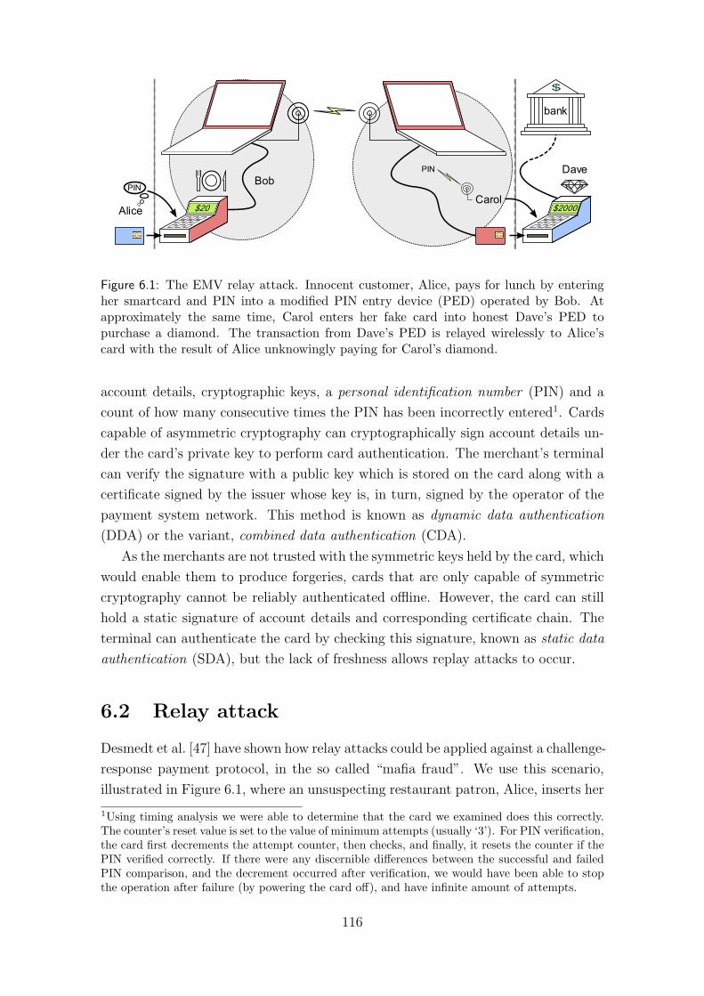
PIN
$2000$20
PIN Dave
CarolAlice
Bob
$
bank
Figure 6.1: The EMV relay attack. Innocent customer, Alice, pays for lunch by enteringher smartcard and PIN into a modified PIN entry device (PED) operated by Bob. Atapproximately the same time, Carol enters her fake card into honest Dave’s PED topurchase a diamond. The transaction from Dave’s PED is relayed wirelessly to Alice’scard with the result of Alice unknowingly paying for Carol’s diamond.
account details, cryptographic keys, a personal identification number (PIN) and a
count of how many consecutive times the PIN has been incorrectly entered1. Cards
capable of asymmetric cryptography can cryptographically sign account details un-
der the card’s private key to perform card authentication. The merchant’s terminal
can verify the signature with a public key which is stored on the card along with a
certificate signed by the issuer whose key is, in turn, signed by the operator of the
payment system network. This method is known as dynamic data authentication
(DDA) or the variant, combined data authentication (CDA).
As the merchants are not trusted with the symmetric keys held by the card, which
would enable them to produce forgeries, cards that are only capable of symmetric
cryptography cannot be reliably authenticated offline. However, the card can still
hold a static signature of account details and corresponding certificate chain. The
terminal can authenticate the card by checking this signature, known as static data
authentication (SDA), but the lack of freshness allows replay attacks to occur.
6.2 Relay attack
Desmedt et al. [47] have shown how relay attacks could be applied against a challenge-
response payment protocol, in the so called “mafia fraud”. We use this scenario,
illustrated in Figure 6.1, where an unsuspecting restaurant patron, Alice, inserts her
1Using timing analysis we were able to determine that the card we examined does this correctly.The counter’s reset value is set to the value of minimum attempts (usually ‘3’). For PIN verification,the card first decrements the attempt counter, then checks, and finally, it resets the counter if thePIN verified correctly. If there were any discernible differences between the successful and failedPIN comparison, and the decrement occurred after verification, we would have been able to stopthe operation after failure (by powering the card off), and have infinite amount of attempts.
116

smartcard into a PIN entry device (PED) in order to pay a $20 charge, which is
presented to her on the display. The PED looks just like any one of the numerous
types of PEDs she has used in the past. This particular PED, however, has had its
original circuitry replaced by the waiter, Bob, and instead of being connected to the
bank, it is connected to a laptop placed behind the counter. As Alice inserts her
card into the counterfeit PED, Bob sends a message to his accomplice, Carol, who
is about to pay $2 000 for a diamond ring at Dave’s jewelery shop. Carol inserts a
counterfeit card into Dave’s PED, which looks legitimate to Dave, but conceals a
wire connected to a laptop in her backpack.
Bob and Carol’s laptops are communicating wirelessly using mobile-phones or
some other network. The data to and from Dave’s PED is relayed to the restaurant’s
counterfeit PED such that the diamond purchasing transaction is placed on Alice’s
card. The PIN entered by Alice is recorded by the counterfeit PED and is sent, via
a laptop and wireless headset, to Carol who enters it into the genuine PED when
asked. When the transaction is over, the criminals have paid for a diamond ring
using Alice’s money, who got her meal for free, but will be surprised to find the
$2 000 charge on her bank statement.
Despite the theoretical risk being documented, EMV is vulnerable to the relay
attack, as suggested by Anderson et al. [15]. Some believed that engineering dif-
ficulties in deployment would make the attack too expensive, or even impossible.
The following section will show that equipment to implement the attack is readily
available, and costs are within the expected returns of fraud.
6.2.1 Implementation
We chose off-the-shelf components that allowed for fast development rather than
miniaturization or cost-effectiveness. The performance requirements were modest,
with the main requirement being that our custom hardware fit within the PED.
6.2.1.1 Counterfeit PED
Second hand Chip and PIN PEDs are readily available for purchase online and their
sale is not restricted. While some are as cheap as $10, our PED was obtained for $50
from eBay and was ideal for our purposes due to its copious internal space. Even
if they were not so readily available, a plausible counterfeit could be made from
scratch as it is only necessary that it appears legitimate to untrained cardholders.
Instead of reverse engineering the existing circuit, we stripped most internal
hardware except for the keypad and LCD screen, and replaced it with a $200 Xilinx
Spartan-3 small factor, USB-controlled, development board2. We also kept the
2Opal Kelly, “XEM3001 – Xilinx Spartan-3 Integration Module”,http://www.opalkelly.com/products/xem3001/
117

(a) With the exterior intact, the PED’s original internalcircuitry was replaced by a small factor FPGA board (left);FPGA based smartcard emulator (right) connected to coun-terfeit card (front).
(b) Customer view of the PED.Here it is playing Tetris todemonstrate that we have fullcontrol of the display and keypad.
Figure 6.2: Photographs of tampered PED and counterfeit card.
original smartcard reader slot, but wired its connections to a $40 Gemalto USB
GemPC Twin3 reader so we could connect it to the laptop. The result is a PED
with which we can record keypad strokes, display content on the screen and interact
with the inserted smartcard. The PED appears and behaves just like a genuine one
to the customer but cannot communicate with the bank or payment network, as it
could before it was tampered with.
6.2.1.2 Counterfeit card
At the jeweler’s, Carol needs to insert a counterfeit card connected to her laptop
into Dave’s PED. We took a genuine Chip and PIN card and ground down the resin-
covered wire bonds that connect the chip to the back of the card’s pads. With the
pads exposed, using a soldering iron, we ironed into the plastic thin, flat wires to the
edge of the card. The card looks authentic from the top side, but was actually wired
on the back side, as shown in Figure 6.2. The counterfeit card was then connected
through a 1.5 m cable to a $150 Xilinx Spartan-3E FPGA Starter Kit [186, UG230]
board to buffer the communications and translate them between the ISO 7816 and
RS-232 protocols. Since the FPGA is not 5 V tolerant, we use 390 Ω resistors on
the channels that receive data from the card. For the bi-directional I/O channel, we
use the Maxim 1740/1 SIM/smartcard level translator4, which costs less than $2.
3http://www.gemalto.com/products/pc_link_readers/#PC_Twin4http://www.maxim-ic.com/quick_view2.cfm/qv_pk/2174
118

6.2.1.3 Controlling software
The counterfeit PED and card are controlled by separate laptops via USB and RS-
232 interfaces, respectively, using custom software written in Python. The laptops
communicate via TCP over IEEE 802.11b wireless, although in principle this could
be GSM or another wireless protocol. This introduces significant latency, but far
less than would be a problem as the timing critical operations on the counterfeit
card are performed by the FPGA.
One complication of selecting an off-the-shelf USB smartcard reader for the coun-
terfeit PED is that it operates at the application protocol data unit (APDU) level
and buffers an entire command or response before sending it to the smartcard or
the PC. This increases the time between when the genuine PED sends a command
and when the response can be sent. Were the counterfeit terminal to incorporate a
character-level card reader, the partial command code could be sent to the genuine
card and the result examined to determine the direction, but this is not permissible
for APDU level transactions. Hence, other than the fact that the controlling soft-
ware must be told the direction for each of the 14 command codes, the relay attack
is protocol-agnostic and could be deployed against any ISO 7816 based system.
6.2.2 Procedure and timing
EMV offers a large variety of options, but the generality of the relay attack allows
our implementation to account for them all; for simplicity, we will describe the
procedure for the common case in the UK. That is, SDA card authentication (only
the static cryptographic signature of the card details is checked), online transaction
authorization (the merchant will connect to the issuer to verify that adequate funds
are available) and offline plaintext PIN cardholder verification (the PIN entered
by the cardholder is sent to the card, unencrypted, and the card will check its
correctness).
Transaction authorization is accomplished by the card generating an application
cryptogram (AC), which is authenticated by the card’s symmetric key and incorpo-
rates transaction details from the terminal, a card transaction counter, and whether
the PIN was entered correctly. Thus, the issuing bank can confirm that the genuine
card was available and the correct PIN was used.
The protocol can be described in six steps:
Initialization: The card is powered up and returns the answer to reset (ATR).
Then the PED selects one of the card’s possible payment applications.
Read application data: The PED requests card details (account number, name,
expiration date, etc.) and verifies the static signature.
119

Cardholder verification: The cardholder enters the PIN into the merchant’s PED
for verification by the card. If correct, the card returns a success code, otherwise
the cardholder may try again until the maximum number of PIN attempts have
been exceeded.
Generate AC 1: The PED requests an authorization request cryptogram (ARQC)
from the card, which is sent to the issuing bank for verification, that then re-
sponds with the issuer authentication data.
External authenticate: The PED sends the issuer authentication data to the
card.
Generate AC 2: The PED asks the card for a transaction certificate (TC) which
the card returns to the PED if, based on the issuer authentication data and other
internal state, the transaction is approved. Otherwise, it returns an application
authentication cryptogram (AAC), signifying the transaction was denied. The
TC is recorded by the merchant to demonstrate that it should receive the funds.
This flow imposes some constraints on the relay attack. Firstly, Alice must insert
her card before Carol inserts her counterfeit card in order for initialization and read
application data to be performed. Secondly, Alice must enter her PIN before Carol
is required to enter it into the genuine PED. Thirdly, Alice must not remove her
card until the Generate AC 2 stage has occurred. Thus, the two sides of the radio
link must be synchronized, but there is significant leeway as Carol can stall until
needing to insert her card.
After that point, the counterfeit card can request extra time from the terminal,
before sending the first response, by sending a null procedure byte (0x60). The
counterfeit terminal can also delay Alice by pretending to dial-up the bank and
waiting for authorization until Carol’s transaction is complete. All timing critical
sections, such as sending the ATR in response to de-assertion of reset and the en-
coding/decoding of bytes sent on the I/O, are implemented on the FPGA to ensure
a fast enough response. There are wide timing margins between the command and
response, so this is managed in software.
6.2.3 Results
We tested our relay setup with a number of different smartcard readers in order to
test its robustness. Firstly, we used a Chip Authentication Program (CAP) reader,
which is a one-time-password generator for use in online banking, and implements
a subset of the EMV protocol. Specifically, it performs cardholder verification by
checking the PIN and requests an application cryptogram, which may be validated
120

online5. Our relay setup was able to reliably complete transactions, even when we
introduced an extra three seconds of latency between command and response.
The CAP readers we examined use the lower clock frequency range allowed by
ISO 7816 (1 MHz to 1.5 MHz) to lower power consumption. We also tested our relay
setup with a GemPC Twin reader, which operates at 4 MHz. The card reader was
controlled by our own software, which simulates a Chip and PIN transaction. Here,
the relay device also worked without any problems and results were identical to
when the card was connected directly to the reader.
Finally, we developed a portable version of the equipment, and took this to a
merchant with a live Chip and PIN terminal. With the consent of the merchant
and cardholder, we executed the relay attack. In addition to the commands and
responses being relayed, the counterfeit terminal was connected to a laptop which,
through voice-synthesis software, read out the PIN to our “Carol”. The transaction
was completed successfully. The first live demonstration of our equipment operating
wirelessly between a Cambridge restaurant and book store was shown on the UK
consumer rights program BBC Watchdog on 6th February 2007.
6.2.4 Further applications and feasibility
The relay attack is also applicable where “Alice” is not the legitimate card holder,
but a thief who has stolen the card and observed the PIN. To frustrate legal inves-
tigation and fraud detection measures, criminals commonly use cards in a different
country from where they were stolen. Magnetic stripe cards are convenient to use in
this way, as the data can be read and sent overseas, to be written on to counterfeit
cards. However, chip cards cannot be fully duplicated, so the physical card would
need to be mailed, introducing a time window where the cardholder may report the
card stolen or lost.
The relay attack can allow criminals to avoid this delay by making the card
available online using a card reader and a computer connected to the Internet. The
criminal’s accomplice in another country could connect to the card remotely and
place transactions with a counterfeit one locally. The timing constraints in this
scenario are more relaxed as there is no customer expecting to remove their genuine
card. Finally, in certain types of transactions, primarily with unattended terminals,
the PIN may not be required, making this attack easier still.
APACS6, the UK payment association, said at the time we demonstrated the at-
tack that they are unaware of any cases of relay attacks being used against Chip and
PIN in the UK [16]. The likely reason is that even though the cost and the technical
5We analyze the security properties of these devices, and reversed engineered the protocol theyuse in Drimer et al. [59].6In June 2009, the “Association for Payment Clearing Services” re-branded itself to be called the“UK Payment Administration”.
121

expertise that are required for implementing the attack are relatively low, there are
easier ways to defeat the system. Methods such as card counterfeiting/theft, mail
interception, and cardholder impersonation are routinely reported and are more
flexible in deployment.
These security holes are gradually being closed, but card fraud remains a lucra-
tive industry – in 2008 £610m of fraud was suffered by UK banks7. Criminals will
adapt to the new environment and, to maintain their income, will likely resort to
more technically demanding methods, so now is the time to consider how to prevent
relay attacks for when that time arrives.
6.3 Defenses
The previous section described how feasible it is to deploy relay attacks against Chip
and PIN and other smartcard based authorization systems in practice. Thus, sys-
tem designers must develop mitigation techniques while, for economic consideration,
staying within the deployed EMV framework as much as possible.
6.3.1 Non-solutions
In this section we describe a number of solutions that are possible, or have been
proposed, against our attack and evaluate their overall effectiveness.
Tamper-resistant terminals. A pre-requisite of our relay attack is that Alice
will insert her card and enter her PIN into a terminal that relays these details to
the remote attacker. The terminal, therefore, must either be tampered with or be
completely counterfeit, but still acceptable to cardholders. This implies a potential
solution – allow the cardholder to detect malicious terminals so they will refuse to
use them.
This is not feasible. Although terminals do implement internal tamper-responsive
measures, when triggered, they only delete keys and other data without leaving
visible evidence to the cardholder. Tamper-resistant seals could be inspected by
customers, but Johnston et al. [99] have shown that many types of seals can be
trivially bypassed. Better seals could be used, but without training to detect tam-
pering, they too will be ineffective. It seems infeasible, and unjust, to require that
all customers be trained to detect tampering, thus also making them responsible for
ant fraud they did not detect. In addition, time-pressure and awkward placement
of terminals can make it extremely difficult for even the most observant customers
to check for tampering, and act on it.
Even if seals were effective, there are, as of July 2009, 289 “Payment Card
Industry PIN Entry Device” (PCI-PED) approved terminal designs from 99 different
7APACS, “2008 fraud figures announced by APACS”, http://www.apacs.org.uk/09_03_19.htm
122

vendors8, so cardholders cannot be expected to identify them all. Were there only
one terminal design, the use of counterfeit terminals would have to be prevented,
which raises the same problems as tamper-resistant seals. Finally, with the large
sums of money netted by criminals from card fraud, fabricating plastic parts is well
within their budget.
Imposing additional timing constraints. While relay attacks will induce extra
delays between commands being sent by the terminal and responses being received,
existing smartcard systems are tolerant to very high latencies. We have successfully
tested our relay device after introducing a three second delay into transactions, in
addition to the inherent delay of our design. This extra round-trip time could be
exploited by an attacker 450 000 km away, assuming that signals propagate at the
speed of light. Perhaps, then, attacks could be prevented by requiring that cards
reply to commands precisely after a fixed delay. Terminals could then confirm that
a card responds to commands promptly and will otherwise reject a transaction.
Other than the generate AC command, which includes a terminal nonce, the
terminal’s behavior is very predictable. So an attacker could preemptively request
these details from the genuine card then send them to the counterfeit card where
they are buffered for quick response. Thus, the value of latency as a distance measure
can only be exploited at the generate AC stages. Furthermore, Clulow et al. [37]
and Hancke and Kuhn [85] show how wireless distance bounding protocols, based
on channels which were not designed for the purpose, can be circumvented. Their
analysis applies equally well to wired protocols such as ISO 7816.
To hide the latency introduced by mounting the relay attack, the attacker aims
to sample signals early and send signals late, while still maintaining their accuracy.
In ISO 7816, cards and terminals are required to sample the signal between the 20%
and 80% portion of the bit-time and aim to sample at the 50% point. However, an
attacker with sensitive equipment could sample near the beginning, and send their
bit late. The attacker then gains 50% of a bit-width in both directions, which at a
5 MHz clock is 37 µs, or 11 km.
The attacker could also over-clock the genuine card so the responses are returned
more quickly. If a DES calculation takes a 100 ms, a 1% increase would give a 300 km
distance advantage. Even if the calculation time was fixed, and only receiving the
response from the card could be accelerated, the counterfeit card could preemptively
reply with the predictable 11 bytes (2 byte response code, 5 byte read more com-
mand, 2 byte header and 2 byte counter) each taking 12 bit-widths (start, 8 data
bits, stop and 2 bits guard time). At 5 MHz + 1% this gives the attacker 98 µs, or
29 km.
8PCI Security Standard Council, “Approved PIN Entry Devices”,https://www.pcisecuritystandards.org/security_standards/ped/pedapprovallist.html
123
One EMV-specific problem is that the contents of the payload in the generate
AC command are specified by the card in the card risk management data object list
(CDOL). Although the terminal nonce should be at the end of the message in order
to achieve maximum resistance to relay attacks, if the CDOL is not signed (as do
some of the cards we examined), the attacker could substitute the CDOL for one
requesting the challenge near the beginning. Upon receiving the challenge from the
terminal, the attacker can then send this to the genuine card. Other than the nonce,
the rest of the generate AC payload is predictable, so the counterfeit terminal can
restore the challenge to the correct place, fill in the other fields and send it to the
genuine card. Thus, the genuine card will send the correct response, even before the
terminal thinks it has finished sending the command. A payload will be roughly 30
bytes, which at 5 MHz gives 27 ms and a 8 035 km distance advantage.
Nevertheless, eliminating needless tolerance to response latency would decrease
the options available to the attacker. If it were possible to roll out this modification
to terminals as a software upgrade, it might be expedient to plan for this alteration
to be quickly deployed in reaction to actual use of the relay attack. While we have
described how this countermeasure could be circumvented, attackers who build and
test their system with high latency would be forced to re-architect it if the acceptable
latency of deployed terminals were decreased without warning.
6.3.2 Procedural improvements
Today, merchants and till operators are accustomed to looking away while customers
enter their PIN and seldom handle the card at all, while customers are often advised
not to allow anyone but themselves to handle the card because of card skimming.
In the case of relay attacks, this assists the criminal, not the honest customer or
merchant. If the merchant examined the card, even superficially, he would detect
the relay attack, as we implemented it, by spotting the wires. That said, it is not
infeasible that an RFID proximity card could be modified to relay data wirelessly
to a local receiver and therefore appear to be a genuine one.
A stronger level of protection can be achieved if, after the transaction is complete,
the merchant checks not only that the card presented is legitimate, but also that
the embossed card number matches the one on the receipt. In the case of the relay
attack, the receipt will show the victim’s card number, whereas the counterfeit card
will show the a different one. For these to match, the criminal must have appropriate
blank cards and an embossing machine, in addition to knowing the victim’s card
number in advance.
124

6.3.3 Hardware alterations
Cardholders may use their own trusted devices as part of the transaction [17].
The electronic attorney “man-in-the-middle defense”, suggested by Anderson and
Bond [11], is inserted into the terminal’s card slot while the customer inserts their
card into the device. The device can display the transaction value as it is parsed from
the data sent from the terminal, allowing the customer to verify that she is charged
the expected amount. If the customer approves the transaction, she presses a button
on the electronic attorney itself, which allows the protocol to proceed. This trusted
user interface is necessary, since if a PIN was used as normal, a criminal could place a
legitimate transaction first, which is accepted by the customer, but with knowledge
of the PIN a subsequent fraudulent one can be placed. Alternatively, one-time-PINs
could be used, but at a cost in usability.
Because the cardholder controls the electronic attorney, and it protects the card-
holder’s interests, the incentives are properly aligned. Market forces in the busi-
ness of producing and selling these devices should encourage security improvements.
However, this extra device will increase costs, increase complexity and may not be
approved of by banking organizations. Additionally, criminals may attempt to dis-
courage their use, either explicitly or by arranging the card slot so the use of a
electronic attorney is difficult. A variant of the trusted user interface is to integrate
a display into the card itself [19].
Another realization of the trusted user interface for payment applications is to
integrate the functionality of a smartcard into the customer’s mobile phone. This can
allow communication with the merchant’s terminal using near field communications
(NFC) [93]. This approach is already under development and has the advantage
of being a customer-controlled device with a large screen and convenient keypad,
allowing the merchant’s name and transaction value to be shown and once authorized
by the user, entry of the PIN. Wireless communications also ease the risk of a
malicious merchant arranging the terminal so that the trusted display device is not
visible. Although mobile phones are affordable and ubiquitous, they may still not
be secure enough for payment applications if they can be targeted by malware.
6.4 Distance bounding
None of the techniques detailed in Section 6.3.1 are adequate to completely defeat
relay attacks. They are either impractical (tamper-resistant terminals), expensive
(adding extra hardware) or circumventable (introducing tighter timing constraints
and requiring merchants to check card numbers). Due to the lack of a customer-
trusted user interface on the card, there is no way to detect a mismatch between
the data displayed on the terminal and the data authorized by the card. However,
125

relay attacks can be foiled if either party can securely establish the position of the
card which is authorizing the transaction, relative to the terminal processing it.
Absolute global positioning is infeasible due to the cost and form factor require-
ments of smartcards being incompatible with GPS, and also because the civilian
version is not resistant to spoofing [115]. However, it is possible for the terminal
to securely establish a maximum distance bound, by measuring the round-trip-time
between it and the smartcard; if this time is too long, an alarm would be triggered
and the transaction refused. Despite the check being performed at the merchant
end, the incentive-compatibility problem is lessened because the distance verifica-
tion is performed by the terminal and does not depend on the sales assistant being
diligent.
The approach of preventing relay attacks by measuring round-trip-time was first
proposed by Beth and Desmedt [22] but Brands and Chaum [25] described the first
concrete protocol. Hancke [83] provides a comprehensive analysis of existing distance
bounding protocols. The cryptographic exchange in our proposal is based on the
Hancke-Kuhn protocol [83, 84], because it requires fewer steps than others, and
it is more efficient if there are transmission bit errors compared to Brands-Chaum.
However, the Hancke-Kuhn protocol was proposed for ultra-wideband radio (UWB),
whereas we require synchronous half-duplex wired transmission.
One characteristic of distance-bounding protocols, unlike most others, is that the
physical transmission layer is security-critical and tightly bound to the other layers,
so care must be taken when changing the transmission medium. Wired transmission
introduces some differences, which must be taken into consideration. Firstly, to avoid
circuitry damage or signal corruption, in a wired half duplex transmission, contention
(both sides driving the I/O at the same time) must be avoided. Secondly, whereas
UWB only permits the transmission of a pulse, a wire allows a signal level to be
maintained for an extended period of time. Hence, we may skip the initial distance-
estimation stage of the Hancke-Kuhn setup and simplify our implementation; no
other modifications to the protocol itself were made.
While in this section we will describe our implementation in terms of EMV,
implemented to be compatible with ISO 7816, it should be applicable to any wired,
half-duplex synchronous serial communication line.
6.4.1 Protocol
In EMV, only the card authenticates itself to the terminal so we follow this prac-
tice. Using the terminology of Hancke-Kuhn, the smartcard is the prover P , and
the terminal is the verifier V . This is also appropriate because the Hancke-Kuhn
protocol puts more complexity in the verifier than the prover, and terminals are sev-
eral orders of magnitude more expensive and capable than the cards. The protocol
126

A 3 8 F 6 D 7 5
Ci : 1010 0011 1000 1111 0110 1101 0111 0101
R0i : x0x0 11xx x011 xxxx 0xx1 xx1x 1xxx 1x0x
R1i : 1x0x xx10 1xxx 0001 x10x 01x0 x111 x1x0
RCii : 1000 1110 1011 0001 0101 0110 1111 1100
8 E B 1 5 6 F C
Table 6.1: Example of the rapid bit-exchange phase of the distance bounding protocol.For clarity, x is shown instead of the response bits not sent by the prover. The left mostbit is sent first.
is described as follows:
Initialization :
V → P : NV ∈ 0, 1a
P → V : NP ∈ 0, 1a
P : (R0i ||R1
i ) = MACK(NV , NP ) ∈ 0, 12b
Rapid bit-exchange(i = 1,...,b):
V → P : Ci ∈ 0, 1P → V : RCi
i ∈ 0, 1
At the start of the initialization phase, nonces and parameters are exchanged over
a reliable data channel, with timing not being critical. NV and NP provide freshness
to the transaction in order to prevent replay attacks, with the latter preventing a
middle-man from running the complete protocol twice between the two phases using
the same NV and complementary Ci and thus, obtain both R0i and R1
i . The prover
produces a MAC under its key K using a keyed pseudo-random function, the result
of which is split into two shift registers, R0i and R1
i .
In the timing-critical rapid bit-exchange phase, the maximum distance between
the two participants is determined. V sends a cryptographically secure pseudoran-
dom single-bit challenge Ci to P , which in turn immediately responds with RCii , the
next single-bit response, from the corresponding shift register. A transaction of a
32 bit exchange is shown in Table 6.1.
If a symmetric key is used, this will require an online transaction to verify the
result because the terminal does not store K. If the card has a private/public
key pair, a session key can be established and the final challenge-response can also
be verified offline. The values a and b, the nonce and shift register bit lengths,
respectively, are security parameters that are set according to the application and
are further discussed in Section 6.4.4.
This exchange succeeds in measuring distance because it necessitates that a
127

Symbol Description
CLKV , fV Verifier’s clock, frequency; determines distance resolutionCLKV→P , fP Prover’s clock, frequency; received from verifierDRVC While asserted the challenge is transmittedtn Length of time verifier drives the challenge on to the I/OSMPLC Prover samples challenge on rising edgetm Time between assertion of DRVC and assertion of CLKV→P
DRVR Prover transmits responsetp Amount of delay applied to SMPLC
SMPLR Verifier samples response on rising edgetq Time from assertion of CLKV→P to rising edge of SMPLR;
determines upper bound of prover’s distancetd Propagation delay through distance d
Table 6.2: Signals and their associated timing parameters.
response bit arrive at a certain time after the challenge bit has been sent. When the
protocol execution is complete, V ’s response register, RCii , is verified by the terminal
or bank to determine if the prover is within the allowed distance for the transaction.
6.4.2 Implementation
ISO 7816, our target application, dictates that the smartcard (prover) is a low
resource device, and therefore, should have minimal additions in order to keep costs
down; this was our prime constraint. The terminal (verifier), on the other hand, is
a capable, expensive device that can accommodate moderate changes and additions
without adversely affecting its cost. Of course, the scheme must be secure to all
attacks devised by a highly capable adversary that can relay signals at the speed of
light, is able to ensure perfect signal integrity, and can clock the smartcard at higher
frequencies than it was designed for. We assume, however, that this attacker does
not have access to the internal operation of the terminal and that extracting secret
material out of the smartcard, or interfering with its security critical functionality,
is not economical considering the returns from the fraud.
6.4.3 Circuit elements and signals
For this section refer to Table 6.2 for signal names and their function, Figure 6.4 for
the circuit diagram and Figure 6.3 for the signal waveforms.
Clocks and frequencies. As opposed to the prover, the verifier may operate at
high frequencies. We implemented the protocol such that one clock cycle of the
verifier’s operating frequency fV determines the distance resolution. Since signals
cannot travel faster than the speed of light c the upper-bound distance resolution is,
128
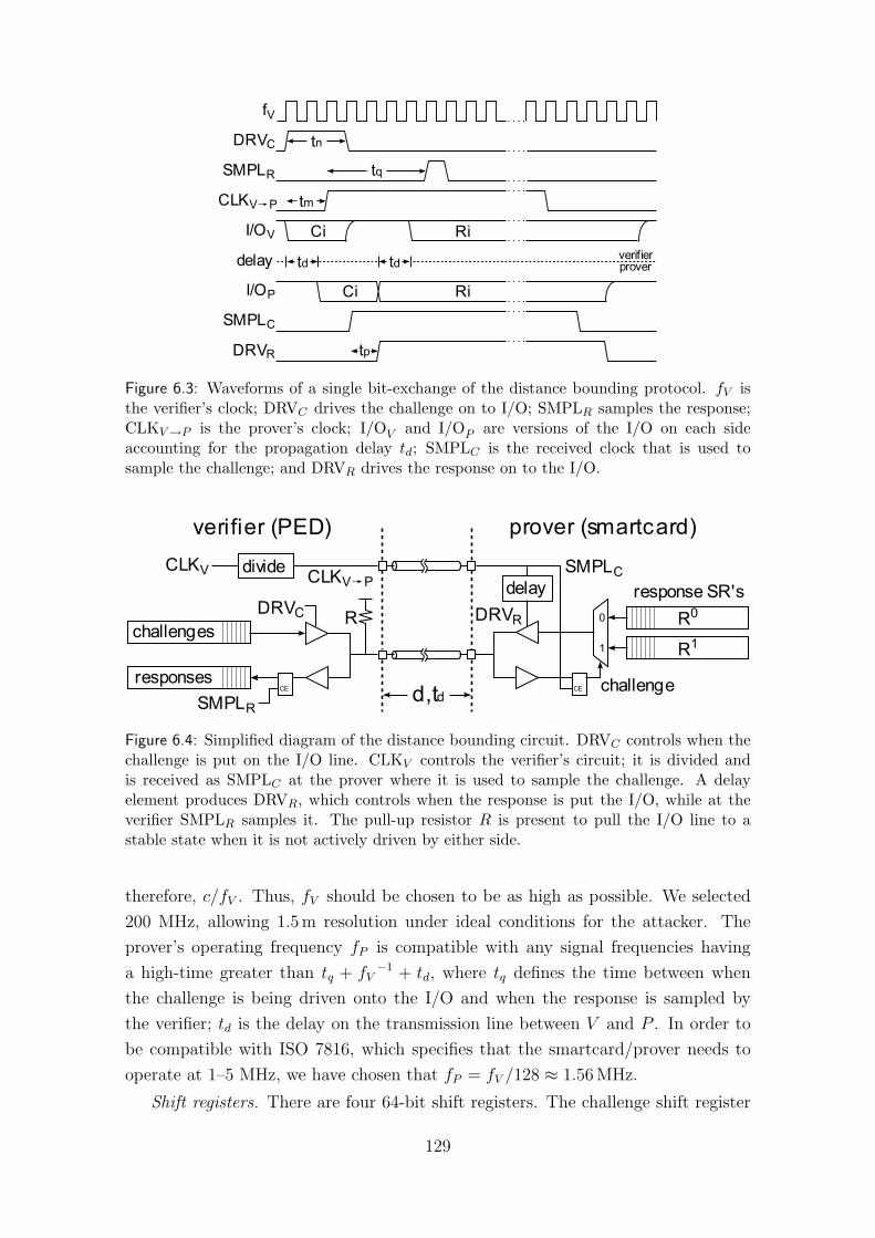
SMPLC
tn
tm
tp
delay
Ci
Ci Ri
RiI/OV
I/OP
td
fV
CLKV P
DRVR
tq
DRVC
SMPLR
td verifierprover
Figure 6.3: Waveforms of a single bit-exchange of the distance bounding protocol. fV isthe verifier’s clock; DRVC drives the challenge on to I/O; SMPLR samples the response;CLKV→P is the prover’s clock; I/OV and I/OP are versions of the I/O on each sideaccounting for the propagation delay td; SMPLC is the received clock that is used tosample the challenge; and DRVR drives the response on to the I/O.
SMPLC
DRVR
delay
R0
R1
SMPLR
DRVC
divideCLKV
response SR's
challengeCECE
0
1
CLKV P
R
verifier (PED) prover (smartcard)
d,tdresponses
challenges
Figure 6.4: Simplified diagram of the distance bounding circuit. DRVC controls when thechallenge is put on the I/O line. CLKV controls the verifier’s circuit; it is divided andis received as SMPLC at the prover where it is used to sample the challenge. A delayelement produces DRVR, which controls when the response is put the I/O, while at theverifier SMPLR samples it. The pull-up resistor R is present to pull the I/O line to astable state when it is not actively driven by either side.
therefore, c/fV . Thus, fV should be chosen to be as high as possible. We selected
200 MHz, allowing 1.5 m resolution under ideal conditions for the attacker. The
prover’s operating frequency fP is compatible with any signal frequencies having
a high-time greater than tq + fV−1 + td, where tq defines the time between when
the challenge is being driven onto the I/O and when the response is sampled by
the verifier; td is the delay on the transmission line between V and P . In order to
be compatible with ISO 7816, which specifies that the smartcard/prover needs to
operate at 1–5 MHz, we have chosen that fP = fV /128 ≈ 1.56 MHz.
Shift registers. There are four 64-bit shift registers. The challenge shift register
129

Figure 6.5: The Xilinx XUP board [186, UG069] with a Virtex-II PRO 30 FPGA onwhich the distance bounding design was implemented. Both verifier and prover reside onthe same chip connected only by two same-length transmission lines for I/O and clock.Measurements were taken at exposed I/O vias on the back side of the PCB, as close aspossible to I/O pins.
is clocked by CLKV and is shifted one clock cycle before it is driven on to the I/O
line by DRVC . The verifier’s response shift register is also clocked by CLKV and
is shifted on the rising edge of SMPLR. On the prover side, the two response shift
registers are clocked and shifted by SMPLC .
Bi-directional I/O. The verifier and prover communicate using a bi-directional
I/O with tri-state buffers at each end. These buffers are controlled by the signals
DRVC and DRVR and are implemented such that only one side drives the I/O line
at any given time in order to prevent contention. This is a consequence of adapting
the Hancke-Kuhn protocol to a wired medium, and implies that the duration of
the challenge must be no longer than necessary, so as to obtain the most accurate
distance bound. A pull-up is also present, as with the ISO 7816 specification, to
maintain a high state when the line is not driven by either side.
Timing. A timing diagram of a single challenge-response exchange is shown
in Figure 6.3. The circuit shown in Figure 6.4 was implemented on an FPGA
using Verilog (not all control signals are shown for simplicity). Since we used a
single chip, the I/O and clock lines were “looped-back” using transmission wires of
varying lengths to simulate the distance between the verifier and prover as shown
in Figure 6.5.
The first operation is clocking the challenge shift register (not shown), which
is driven on to the I/O line by DRVC on the following fV clock cycle for a period
tn. tn should be made long enough to ensure that the prover can adequately and
reliably sample the challenge, and as short as possible to allow the response to
be rapidly sent while not causing contention. The clock sent to P , CLKV→P , is
asserted tm after the rising edge of DRVC . Both CLKV→P and the I/O line have the
130
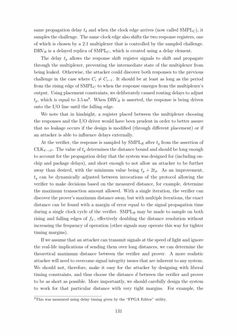
same propagation delay td and when the clock edge arrives (now called SMPLC), it
samples the challenge. The same clock edge also shifts the two response registers, one
of which is chosen by a 2:1 multiplexer that is controlled by the sampled challenge.
DRVR is a delayed replica of SMPLC , which is created using a delay element.
The delay tp allows the response shift register signals to shift and propagate
through the multiplexer, preventing the intermediate state of the multiplexer from
being leaked. Otherwise, the attacker could discover both responses to the previous
challenge in the case where Ci 6= Ci−1. It should be at least as long as the period
from the rising edge of SMPLC to when the response emerges from the multiplexer’s
output. Using placement constraints, we deliberately caused routing delays to adjust
tp, which is equal to 3.5 ns9. When DRVR is asserted, the response is being driven
onto the I/O line until the falling edge.
We note that in hindsight, a register placed between the multiplexer choosing
the responses and the I/O driver would have been prudent in order to better assure
that no leakage occurs if the design is modified (through different placement) or if
an attacker is able to influence delays externally.
At the verifier, the response is sampled by SMPLR after tq from the assertion of
CLKV→P . The value of tq determines the distance bound and should be long enough
to account for the propagation delay that the system was designed for (including on-
chip and package delays), and short enough to not allow an attacker to be further
away than desired, with the minimum value being tp + 2td. As an improvement,
tq can be dynamically adjusted between invocations of the protocol allowing the
verifier to make decisions based on the measured distance, for example, determine
the maximum transaction amount allowed. With a single iteration, the verifier can
discover the prover’s maximum distance away, but with multiple iterations, the exact
distance can be found with a margin of error equal to the signal propagation time
during a single clock cycle of the verifier. SMPLR may be made to sample on both
rising and falling edges of fV , effectively doubling the distance resolution without
increasing the frequency of operation (other signals may operate this way for tighter
timing margins).
If we assume that an attacker can transmit signals at the speed of light and ignore
the real-life implications of sending them over long distances, we can determine the
theoretical maximum distance between the verifier and prover. A more realistic
attacker will need to overcome signal integrity issues that are inherent to any system.
We should not, therefore, make it easy for the attacker by designing with liberal
timing constraints, and thus choose the distance d between the verifier and prover
to be as short as possible. More importantly, we should carefully design the system
to work for that particular distance with very tight margins. For example, the
9This was measured using delay timing given by the “FPGA Editor” utility.
131
various terminals we have tested were able to transmit/drive a signal through a two
meter cable, although the card should at most be a few centimeters away. Weak
I/O drivers could be used to degrade the signal when an extension is applied (our
I/O drivers are set to 8 mA strength). The value of d also determines most of the
timing parameters of the design, and as we shall see next, the smaller these are, the
harder it will be for the attacker to gain an advantage.
6.4.4 Possible attacks on distance bounding
Although, following from our previous assumptions, the attacker cannot get access to
more than about half the response bits, there are ways he may extend the distance
limit before a terminal will detect the relay attack. This section discusses which
options are available, and their effectiveness in evading defenses.
Guessing attack. Following the initialization phase, the attacker can initiate the
bit-exchange phase before the genuine terminal has done so. As the attacker does
not know the challenge at this stage, he will, on average, guess 50% of the challenge
bits correctly and so receive the correct response for those. For the ones where the
challenge was guessed incorrectly, the response is effectively random, so there is still
a 50% chance that the response will be correct. Therefore the expected success rate
of this technique is 75%.
Since our tests show a negligible error rate, the terminal may reject any response
with a single bit that is incorrect. In our prototype, where the response registers
are 64 bits each, the attacker will succeed with probability (34)64 ≈ 1 in 226. The
size of the registers is a security parameter that can be increased according to the
application, while the nonces assure that the attacker can only guess once.
Replay. If the attacker can force the card to perform two protocol runs, with the
same nonces used for both, then all bits of the response can be extracted by sending
all 1’s on the first iteration and all 0’s on the second. We resist this attack by
selecting the protocol variant mentioned by Hancke and Kuhn [84], where the card
adds its own nonce. This is cheap to do within EMV since a transaction counter is
already required by the rest of the protocol. If this is not desired then provided the
card cannot be clocked at twice its intended frequency, the attacker will not be able
to extract all bits in time. This assumes that the time between starting the distance
bounding protocol, and the earliest time the high-speed stage can start, is greater
than the latter’s duration.
Early bit detection and deferred bit signaling. The card will not sample the
terminal’s challenge until tm+d after the challenge is placed on the I/O line. This is
to allow an inexpensive card to reliably detect the signal but, as Clulow et al. [37]
suggest, an attacker could detect the signal immediately. By manipulating the clock
provided to the genuine card, and using high-quality signal drivers, the challenge
132
could be sent to the card with shorter delay.
Similarly, the terminal will wait tq between sending the challenge and sampling
the response, to allow for the round trip signal propagation time, and wait until the
response signal has stabilized. Again, with reduced reliability the response could be
sent from the card just before the terminal samples. The attacker, however, cannot
do so any earlier than tp after the card has sampled the challenge, and the response
appears on the I/O.
Delay-line manipulation. The card may include the value of tp in its signed data,
so the attacker cannot make the terminal believe that the value is larger than the
card’s specification. However, the attacker might be able to reduce the delay, for
example by cooling the card. If it can be reduced to the point that the multiplexer
or latch has not settled, then both potential responses may be placed on to the I/O
line, violating our assumptions.
However, if the circuit is arranged so that the delay will be reduced only if the
reaction of the challenge latch and multiplexer is improved accordingly, the response
will still be sent out prematurely. This gives the attacker extra time, so should be
prevented. If temperature compensated delay lines are not economic, then they
should be as short as possible to reduce this effect.
In fact, in a custom circuit, tp may be so small (less than 1 ns), that the terminal
could just assume it is zero. This will mean that the terminal will believe all cards
are slightly further away than they really are, but will avoid the value of tp having
to be included in the signed data.
Combined attacks. For an attacker to gain a better than 1 in 226 probability
of succeeding in the challenge response protocol, the relay attack must take less
than tm+q time. In practice, an attacker will not be able to sample or drive the
I/O line instantaneously and the radio-link transceiver or long wires will introduce
latency, so the attacker would need to be much closer than this limit. A production
implementation on an ASIC would be able to give better security guarantees and be
designed to tighter specifications than were available on the FPGA for our prototype.
6.4.5 Results
We have developed a versatile implementation that requires only modest modifi-
cation to currently deployed designs. Our distance bounding scheme was success-
fully implemented and tested on an FPGA for 2.0, 1.0, and 0.3 meter transmission
lengths, although it can be modified to work for any distance and tailored to any
end application. To verify the logical correctness of the design (observing wrong re-
sponses, for example) we used the internal logic analyzer “ChipScope” [186, UG029].
Oscilloscope traces of a single bit challenge-response exchange over a 50 Ω, 30 cm
printed circuit board transmission line are shown in Figure 6.6; Figure 6.5 shows
133

volta
ge (
V)
time since start of exchange (µµs)
0 10 20 30 40 50
0
1
2
3
(a) I/OV trace of a 64-bit exchange with position of (b) indicated by • on the x axis.
−10 0 10 20 30 40
0.0
0.5
1.0
1.5
2.0
2.5
3.0
3.5
volta
ge (
V)
time since challenge sent by verifier (ns)
CLKp
Prover samples Verifier samples
t d
t n
tm ++ t d
t p ++ t d
tqfail −− t d
t qpass −− t d
I OvI Op
Challenge sent Response received
0 5 10distance at speed of light in vacuum (m)
(b) Single bit exchange, challenge is 1 and response is 0.
Figure 6.6: Oscilloscope trace from the bit-exchange phase of the distance bounding pro-tocol. Delay is introduced by a 30 cm transmission line between the verifier and prover.Timing parameters are tn = 10 ns, tm = 5 ns, tp = 8 ns (including internal and I/O delays).Two values of tq are shown, one where the bit was correctly received tqpass = 20 ns andone where it was not, tqfail
= 15 ns. td was measured to be 2.16 ns which over a 30 cm wirecorresponds to propagation velocity of 1.4 × 10⁸ m/s. Note that before the challenge issent, the trace is slowly rising above ground level; this is the effect of the pull-up resistoras also seen in (a) after the protocol completes. Also, the shown signals were probed atthe FPGA I/Os and do not precisely represent when they actually appear inside of it,so in actuality the FPGA will “see” the falling edge shown in (b) slightly after what isrepresented in the figure.
134

the FPGA board and experimental setup. In this case, the challenge is 1 and the
response is 0 with indicators where SMPLR has sampled the response. The first,
after tqfail= 15 ns has sampled too early while the second, tqpass = 20 ns, which is
a single period of fV later, has correctly sampled the 0 as the response. The delay
td = 2.16 ns, can also be seen and is, of course, due to the length of the transmission
line. If the attacker exploited all possible attacks previously discussed and was able
to transmit signals at c, he would need to be within approximately 6 m, although
the actual distance would be shorter for a more realistic attacker.
6.4.6 Costs
The FPGA design of both the verifier and prover as shown in Figure 6.4 consumes
37 flip-flops and 93 look-up tables: 64 for logic, 13 route-throughs, and 16 as shift
registers (4 cascaded 16-bit LUTs for each), which is extremely compact. However,
it is difficult to estimate the cost of an ASIC implementation with these figures
as there is no reliable conversion technique between FPGA resource utilization and
ASIC transistor count, especially since the above numbers are for the core functions,
without the supporting circuitry. It is also hard to estimate the cost in currency
because that changes rapidly with time, production volume, fabrication process, and
many other factors, so we will describe it relative to the resources currently used.
As mentioned, we have made every effort to minimize the circuitry that needs to
be added to the smartcard while being more liberal with the terminal, although for
both the additions can be considered minor. For the smartcard, new commands for
initiating the initialization phase need to be added as well as two shift registers and
a state machine for operating the rapid bit-exchange. Considering that smartcards
already have a few thousand memory cells, this can be considered a minor addition,
especially given that they need to operate at the existing low frequencies of 1–5 MHz.
For the initialization phase, existing circuits can be used such as the DES engine
for producing the content of the response registers. The card’s transaction counter
may be used for the nonce Np.
As for the terminals, their internal operating frequency is unknown to us, but
it is unlikely that it is high enough to achieve good distance resolution. Therefore,
a capable processor and some additional components are required, such as a high
quality oscillator. As an alternative to high frequencies, or when designing for very
short distances, delay lines could be used instead of operating on clock edges, as
originally suggested by Hancke and Kuhn [84]. The distance bounding circuitry
would need to be added to the terminal’s main processor, which consists of two shift
registers and slightly more involved control code than the smartcard’s.
We have described the added cost in terms of hardware but the added time per
transaction and the need to communicate with the bank, refused transactions due to
135
failure, re-issuing cards, and so on, may amount to substantial costs. Only the banks
involved have access to all the necessary information needed to make a reasonable
estimate of these overheads.
6.5 Distance bounding in FPGA applications
Relay attacks can also compromise the security and integrity of FPGA systems.
Here, we link the above discussion with the topic of this thesis and point out po-
tential vulnerabilities, and how they may be resisted using the distance bounding
implementation.
Consider the challenge-response deterrents we discussed in Section 2.3.3, where
the FPGA executes an authentication protocol with a processor that is placed near
it on the PCB. This is meant to prevent the bitstream from being used on any other
system that does not contain that specific authentication device. These schemes,
however, do not prevent the challenges from being relayed to a processor far away.
Cloners may be unlikely to go through the trouble of doing this, though designers
of high security modules need to factor this threat into their analysis. For example,
Graf and Athanas [74] describe an FPGA-based security system where users are
authenticated using tamper-proof tokens, though relay attacks are not considered
and are possible. The FPGA and NVM interface in the secure remote update
scheme presented in Chapter 3 is also potentially vulnerable, though an attack will
violate our assumptions when tamper proofing is required; where it is not, remote
attestation makes the threat insignificant.
The configuration process can be protected from relay attacks by adding a dis-
tance bounding functionality to the FPGA configuration logic and the NVM. The
constraints of ISO 7816 are similar for this scenario: the FPGA (verifier) can ac-
commodate the additional circuitry and the performance that is required, while the
NVM (prover) is cheap and simple, but requires little additional circuitry. The in-
terface is similar as well (when the FPGA behaves as the “master”) as serial NVMs
share at least a clock and data line between them. The implementation needs to
be done carefully, however, so configuration content is tied to the distance bound-
ing process. We leave the exploration of integrating distance bounding into the
configuration process to future research.
136
Chapter 7
Review and outlook
“FPGA security” is still a relatively young field, evolving as new FPGA generations
become more capable and their range of applications grows. This dissertation has
examined the role of volatile FPGAs in security systems. The core aim was to
provide practical security solutions for reconfigurable systems, taking into account
the context in which they are used. In review, these were its main contributions:
Chapter 2: comprehensive review of current research in the field. I discussed and
commented on the current state of research in the field based on my own expe-
riences and insights. Section 2.3.2 also provided an analysis of and motivation
for adding bitstream authentication to FPGA configuration logic.
Chapter 3: flexible protocol for secure remote update of bitstreams over insecure
networks. The protocol is versatile and does not require additional circuitry
to be integrated into the hard-wired configuration logic – thus, it can be used
with existing FPGAs. I anticipate that the protocol will be useful to FPGA
applications where unattended remote update is required.
Chapter 4: source code for three AES implementations and CMAC mode of
operation. I have created an FPGA implementation of the AES block cipher
in an innovative way using embedded blocks (BRAMs and DSPs), minimizing
the use of “traditional” logic elements such as flip-flops and lookup tables. As
far as I am aware, these are the first FPGA implementations of a cryptographic
primitive for which source code was fully released at publication time.
Chapter 5: comparing FPGA implementations should be done with caution. I
used FPGA AES designs to demonstrate the significant variability in perfor-
mance under different implementation conditions, questioning common compar-
ison practices across architectures and implementers. I showed that a single figure
of merit, “throughput”, and the comparative unit of “throughput per slice” are
mostly meaningless without context or qualification – they can be appropriately
137

used only under very specific circumstances. I argued that source code avail-
ability can enable recompilation of compared designs under similar conditions.
I also suggested that common implementation platforms be identified and that
results be evaluated based on meeting target performance, rather than “best
possible performance”.
Chapter 5: reproducible research in light of variability of FPGA designs. I used
experimental evidence to strengthen the argument that an experimental-based
publication is simply an advertisement for the source code or experimental work,
which is the actual contribution. Together with the availability of source code, I
proposed that a reproducibility scale be added to manuscripts’ review process.
Chapter 6: EMV payment system is vulnerable to relay attacks. The demon-
stration exemplified the ease with which relay attacks can violate distance as-
sumptions made by the designers of security systems. The immediate impact of
this demonstration was to allow defrauded cardholders to challenge the banks’
inaccurate assertions regarding the security of the “Chip and PIN” payment
system.
Chapter 6: implementation of a secure distance bounding protocol for wired appli-
cations. I implemented a wired adaptation of the Hancke-Kuhn distance bound-
ing protocol on an FPGA. Using routing delays, I was able to implement the
prover side without a fast clock, thus making the design simple. The design was
able to determine that a prover is at most six meters away. While the imple-
mentation initially targeted ISO 7816-3, it can be extended to many other wired
applications, such as the interface between an FPGA and a configuration storage
device.
Appendix A: a way to securely integrate multiple modules into a single FPGA de-
sign. I proposed a practical way for integrating design modules from distrusting
sources into a single FPGA design, thus enabling the pay-per-use core distribu-
tion model. The main advantage of the scheme is that most of the hardware
and software support already exists, and few additions to configuration logic are
required.
One of the emerging themes from my research is worth pointing out: “context
matters for security”. The literature survey provided a broader context to published
results (power analysis and watermarking, for example). The secure remote update
protocol analysis factored in the way in which it will be used, and what system-
level properties must be maintained for security. Some of these measures are a
compromise between security and cost, although only when set in context can such
measures reassure the engineer that the level of protection is sufficient. The AES
138

implementation results were reported in the perspective of constraints and possible
variability, rather than as a single figure of merit. The relay attack illustrated that
even though smartcard ICs are hard to clone and attack, it is the way in which they
are used that compromised the security of the entire system. Much of the discussion
in Appendix A about secure core integration is dedicated to usability evaluation
of the scheme, rather than to a detailed technical discussion – context provides
a measure for usefulness. During my work on security of and for reconfigurable
systems and of payment systems, I learned that, for the most part, security is all
about context and that it is a mistake to treat a problem in isolation, as it is likely
to lead to broken systems.
I see several interesting directions in which the work presented in this dissertation
can be taken.
Considering that FPGAs are fast becoming “systems on a chip”, better access
control to various parts of the FPGA will become necessary. This will require not
only a simple design separation between modules in the same FPGA, but a dedicated
controller for key management and authentication. One example application is the
ability to have a portion of the FPGA available for end-user programming, while
another portion is only updatable by authorized principals (i.e., system developers).
The combination of the protocol described in Chapter 3 and integration scheme of
Appendix A could be a good starting point.
The secure remote update protocol in Chapter 3 can be extended for partial
reconfiguration at start-up time, but careful security analysis is required. For exam-
ple, what are the properties of the bootloader bitstream, and how are the “missing”
bitstream portions sent, or stored locally. The work can be extended to use a
broadcasting system using public key cryptography, so as to minimize the number
of messages that are specific to individual systems.
The wired distance bounding implementation can be extended for mutual au-
thentication between multiple FPGAs, and the timing margins can be tightened for
better distance resolution using additional connections. Another possibility is to
continue the work in the RF domain.
I do sincerely hope that the discussion in Chapter 5 about reproducibility and
comparability of designs will not go unnoticed. I also hope that the example I set
in Chapter 4 by releasing the source code will be followed by others, and that the
code and methodology will be used for further research.
139

140

Bibliography
[1] A. T. Abdel-Hamid, S. Tahar, and E. M. Aboulhamid. IP watermarking tech-niques: survey and comparison. In IEEE International Workshop on System-on-Chip for Real-Time Applications, 2003. ISBN 0-7695-1929-6.
[2] S. Adee. The hunt for the kill switch. IEEE Spectrum, May 2008. http:
//www.spectrum.ieee.org/may08/6171
[3] D. Agrawal, B. Archambeault, J. R. Rao, and P. Rohatgi. The EMside-channel(s): Attacks and assessment methodologies. Technical Report2001/037, IBM Watson Research Center, 2001.
[4] D. Agrawal, B. Archambeault, J. R. Rao, and P. Rohatgi. The EM side-channel(s). In Cryptographic Hardware and Embedded Systems Workshop,volume 2523 of LNCS, pages 29–45, London, UK, August 2002. Springer-Verlag. ISBN 3-540-00409-2.
[5] Algotronix Ltd. AES G3 data sheet Xilinx edition, October 2007. http:
//www.algotronix-store.com/kb_results.asp?ID=7
[6] Alliance for Gray Market and Counterfeit Abatement. Managing therisks of counterfeiting in the information technology industry, number,August 2006. http://www.agmaglobal.org/press_events/press_docs/
Counterfeit_WhitePaper_Final.pdf
[7] Altera Corp. http://www.altera.com
[8] Altera Corp. Court issues preliminary injunction against Clear Logic in Alteralitigation, number, July 2002. http://www.altera.com/corporate/news_
room/releases/releases_archive/2002/corporate/nr-clearlogic.html
[9] M. S. Anderson, C. J. G. North, and K. K. Yiu. Towards countering therise of the silicon Trojan. Technical Report DSTO-TR-2220, Command, Con-trol, Communication and Intelligence Division (C3ID), Department of De-fence, Australian Government, December 2008. http://www.dsto.defence.
gov.au/publications/scientific_record.php?record=9736
[10] R. J. Anderson. Security engineering: A guide to building dependable dis-tributed systems. John Wiley & Sons, Inc., New York, NY, USA, secondedition, 2008. ISBN 978-0-470-06852-6.
141

[11] R. J. Anderson and M. Bond. The man in the middle defence. In SecurityProtocols Workshop, Cambridge, England, March 2006. Springer. http://
www.cl.cam.ac.uk/~rja14/Papers/Man-in-the-Middle-Defence.pdf
[12] R. J. Anderson and M. G. Kuhn. Tamper resistance – a cautionary note. InUSENIX Workshop on Electronic Commerce Proceedings, pages 1–11, Oak-land, CA, November 1996. USENIX.
[13] R. J. Anderson and M. G. Kuhn. Low cost attacks on tamper resistant devices.In International Workshop on Security Protocols, pages 125–136, London, UK,1998. Springer-Verlag.
[14] R. J. Anderson, M. Bond, J. Clulow, and S. P. Skorobogatov. Cryptographicprocessors – a survey. Technical Report UCAM-CL-TR-641, University ofCambridge, Computer Laboratory, August 2005.
[15] R. J. Anderson, M. Bond, and S. J. Murdoch. Chip and spin, March 2005.http://www.chipandspin.co.uk/spin.pdf
[16] APACS. APACS response to BBC Watchdog and chip and PIN. Press re-lease, February 2007. http://www.chipandpin.co.uk/media/documents/
APACSresponsetoWatchdogandchipandPIN-06.02.07.pdf
[17] N. Asokan, D. Herve, M. Steiner, and M. Waidner. Authenticating publicterminals. Computer Networks, 31(9):861–870, 1999.
[18] K. Austin. Data security arrangements for semiconductor programmable de-vices. United States Patent Office, number 5388157, 1995.
[19] Aveso Inc. Display enabled smart cards. http://www.avesodisplays.com/
[20] B. Badrignans, R. Elbaz, and L. Torres. Secure FPGA configuration archi-tecture preventing system downgrade. In Field Programmable Logic, pages317–322, September 2008.
[21] M. Bellare, P. Rogaway, and D. Wagner. The EAX mode of operation. In FastSoftware Encryption, volume 3017 of LNCS, pages 389–407. Springer, 2004.
[22] T. Beth and Y. Desmedt. Identification tokens – or: solving the chess grand-master problem. In CRYPTO, volume 537 of LNCS, pages 169–177. Springer,August 1990. ISBN 3-540-54508-5.
[23] J. Black. “Authenticated encryption” in Encyclopedia of Cryptography andSecurity, section A, pages 10–21. Authenticated encryption. Springer, 2005.
[24] L. Bossuet, G. Gogniat, and W. Burleson. Dynamically configurable securityfor SRAM FPGA bitstreams. In IEEE Reconfigurable Architectures Workshop,Los Alamitos, CA, USA, April 2004. IEEE Computer Society.
[25] S. Brands and D. Chaum. Distance-bounding protocols. In T. Helleseth,editor, EUROCRYPT ’93: Workshop on the theory and application of cryp-tographic techniques on Advances in cryptology, volume 765 of LNCS, pages344–359. Springer, May 1993.
142

[26] J. Brouchier, N. Dabbous, T. Kean, C. Marsh, and D. Naccache. Thermo-communication. Cryptology ePrint Archive, Report 2009/002, 2009. http:
//eprint.iacr.org/2009/002.pdf
[27] M. Bucci, L. Giancane, R. Luzzi, G. Scotti, and A. Trifiletti. Enhancingpower analysis attacks against cryptographic devices. In Circuits and SystemsSymposium, May 2006.
[28] J. D. R. Buchanan, R. P. Cowburn, A.-V. Jausovec, D. Petit, P. Seem,G. Xiong, D. Atkinson, K. Fenton, D. A. Allwood, and M. T. Bryan. Forgery:‘fingerprinting’ documents and packaging. Nature, 436(7050):475, July 2005.
[29] J. B. Buckheit and D. D. Donoho. Wavelab and reproducible research.Technical Report 474, Department of Statistics, Stanford University, 1995.http://www-stat.stanford.edu/~donoho/Reports/1995/wavelab.pdf
[30] P. Bulens, F.-X. Standaert, J.-J. Quisquater, P. Pellegrin, and G. Rouvroy.Implementation of the AES-128 on Virtex-5 FPGAs. In Progress in Cryptology– AfricaCrypt, pages 16–26. Springer, 2008.
[31] V. Carlier, H. Chabanne, E. Dottax, and H. Pelletier. Electromagnetic sidechannels of an FPGA implementation of AES. Cryptology ePrint Archive,(145), 2004. http://eprint.iacr.org/2004/145.pdf
[32] J. Castillo, P. Huerta, and J. I. Martınez. Secure IP downloading for SRAMFPGAs. Microprocessors and Microsystems, 31(2):77–86, February 2007.
[33] R. Chaves, G. Kuzmanov, S. Vassiliadis, and L. Sousa. Reconfigurable memorybased AES co-processor. In Parallel and Distributed Processing Symposium,pages 192–199. IEEE, April 2006.
[34] Z. Chen, S. Morozov, and P. Schaumont. A hardware interface for hashingalgorithms. Cryptology ePrint Archive, Report 2008/529, 2009. http://
eprint.iacr.org/2008/529.pdf
[35] P. Chodowiec and K. Gaj. Very compact FPGA implementation of the AESalgorithm. In Cryptographic Hardware and Embedded Systems Workshop, vol-ume 2779, pages 319–333. Springer, 2003. ISBN 3540408338.
[36] B. D. Christiansen. FPGA security through decoy circuits. Master’s thesis, AirForce Institute of Technology, Ohio, USA, March 2006. http://stinet.dtic.mil/cgi-bin/GetTRDoc?AD=ADA454021&Location=U2&doc=GetTRDoc.pdf
[37] J. Clulow, G. P. Hancke, M. G. Kuhn, and T. Moore. So near and yet so far:distance-bounding attacks in wireless networks. In L. Buttyan, V. Gligor, andD. Westhoff, editors, Security and Privacy in Ad-hoc and Sensor Networks,volume 4357 of LNCS, Hamburg, Germany, September 2006. Springer.
[38] J. H. Conway. On numbers and games. Academic Press, 1976. ISBN 0-12-186350-6.
143
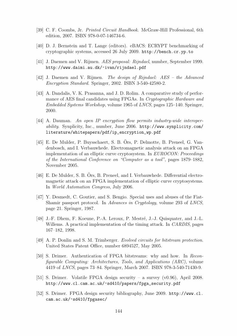
[39] C. F. Coombs, Jr. Printed Circuit Handbook. McGraw-Hill Professional, 6thedition, 2007. ISBN 978-0-07-146734-6.
[40] D. J. Bernstein and T. Lange (editors). eBACS: ECRYPT benchmarking ofcryptographic systems, accessed 26 July 2009. http://bench.cr.yp.to
[41] J. Daemen and V. Rijmen. AES proposal: Rijndael, number, September 1999.http://www.daimi.au.dk/~ivan/rijndael.pdf
[42] J. Daemen and V. Rijmen. The design of Rijndael: AES – the AdvancedEncryption Standard. Springer, 2002. ISBN 3-540-42580-2.
[43] A. Dandalis, V. K. Prasanna, and J. D. Rolim. A comparative study of perfor-mance of AES final candidates using FPGAs. In Cryptographic Hardware andEmbedded Systems Workshop, volume 1965 of LNCS, pages 125–140. Springer,2000.
[44] A. Dauman. An open IP encryption flow permits industry-wide interoper-ability. Synplicity, Inc., number, June 2006. http://www.synplicity.com/
literature/whitepapers/pdf/ip_encryption_wp.pdf
[45] E. De Mulder, P. Buysschaert, S. B. Ors, P. Delmotte, B. Preneel, G. Van-denbosch, and I. Verbauwhede. Electromagnetic analysis attack on an FPGAimplementation of an elliptic curve cryptosystem. In EUROCON: Proceedingsof the International Conference on “Computer as a tool”, pages 1879–1882,November 2005.
[46] E. De Mulder, S. B. Ors, B. Preneel, and I. Verbauwhede. Differential electro-magnetic attack on an FPGA implementation of elliptic curve cryptosystems.In World Automation Congress, July 2006.
[47] Y. Desmedt, C. Goutier, and S. Bengio. Special uses and abuses of the Fiat-Shamir passport protocol. In Advances in Cryptology, volume 293 of LNCS,page 21. Springer, 1987.
[48] J.-F. Dhem, F. Koeune, P.-A. Leroux, P. Mestre, J.-J. Quisquater, and J.-L.Willems. A practical implementation of the timing attack. In CARDIS, pages167–182, 1998.
[49] A. P. Donlin and S. M. Trimberger. Evolved circuits for bitstream protection.United States Patent Office, number 6894527, May 2005.
[50] S. Drimer. Authentication of FPGA bitstreams: why and how. In Recon-figurable Computing: Architectures, Tools, and Applications (ARC), volume4419 of LNCS, pages 73–84. Springer, March 2007. ISBN 978-3-540-71430-9.
[51] S. Drimer. Volatile FPGA design security – a survey (v0.96), April 2008.http://www.cl.cam.ac.uk/~sd410/papers/fpga_security.pdf
[52] S. Drimer. FPGA design security bibliography, June 2009. http://www.cl.
cam.ac.uk/~sd410/fpgasec/
144
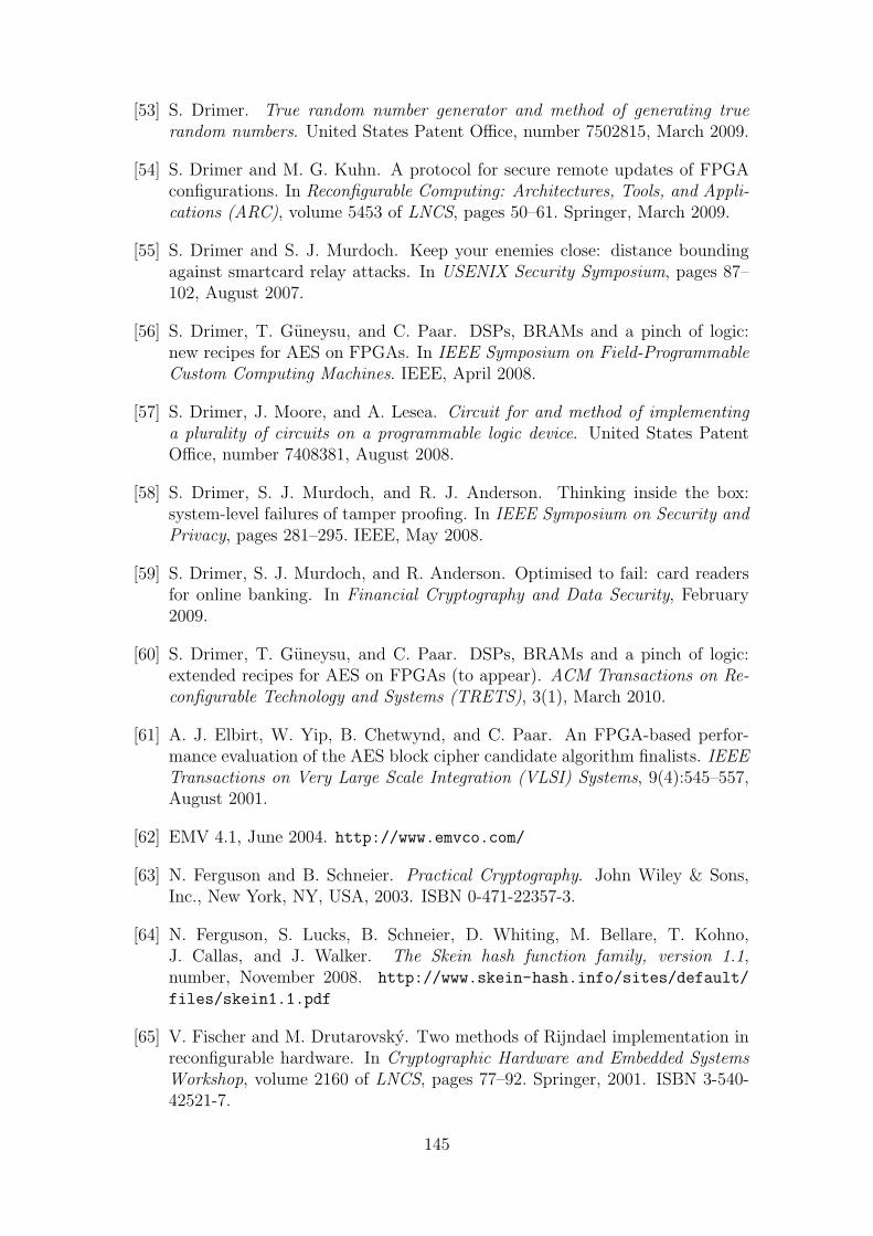
[53] S. Drimer. True random number generator and method of generating truerandom numbers. United States Patent Office, number 7502815, March 2009.
[54] S. Drimer and M. G. Kuhn. A protocol for secure remote updates of FPGAconfigurations. In Reconfigurable Computing: Architectures, Tools, and Appli-cations (ARC), volume 5453 of LNCS, pages 50–61. Springer, March 2009.
[55] S. Drimer and S. J. Murdoch. Keep your enemies close: distance boundingagainst smartcard relay attacks. In USENIX Security Symposium, pages 87–102, August 2007.
[56] S. Drimer, T. Guneysu, and C. Paar. DSPs, BRAMs and a pinch of logic:new recipes for AES on FPGAs. In IEEE Symposium on Field-ProgrammableCustom Computing Machines. IEEE, April 2008.
[57] S. Drimer, J. Moore, and A. Lesea. Circuit for and method of implementinga plurality of circuits on a programmable logic device. United States PatentOffice, number 7408381, August 2008.
[58] S. Drimer, S. J. Murdoch, and R. J. Anderson. Thinking inside the box:system-level failures of tamper proofing. In IEEE Symposium on Security andPrivacy, pages 281–295. IEEE, May 2008.
[59] S. Drimer, S. J. Murdoch, and R. Anderson. Optimised to fail: card readersfor online banking. In Financial Cryptography and Data Security, February2009.
[60] S. Drimer, T. Guneysu, and C. Paar. DSPs, BRAMs and a pinch of logic:extended recipes for AES on FPGAs (to appear). ACM Transactions on Re-configurable Technology and Systems (TRETS), 3(1), March 2010.
[61] A. J. Elbirt, W. Yip, B. Chetwynd, and C. Paar. An FPGA-based perfor-mance evaluation of the AES block cipher candidate algorithm finalists. IEEETransactions on Very Large Scale Integration (VLSI) Systems, 9(4):545–557,August 2001.
[62] EMV 4.1, June 2004. http://www.emvco.com/
[63] N. Ferguson and B. Schneier. Practical Cryptography. John Wiley & Sons,Inc., New York, NY, USA, 2003. ISBN 0-471-22357-3.
[64] N. Ferguson, S. Lucks, B. Schneier, D. Whiting, M. Bellare, T. Kohno,J. Callas, and J. Walker. The Skein hash function family, version 1.1,number, November 2008. http://www.skein-hash.info/sites/default/
files/skein1.1.pdf
[65] V. Fischer and M. Drutarovsky. Two methods of Rijndael implementation inreconfigurable hardware. In Cryptographic Hardware and Embedded SystemsWorkshop, volume 2160 of LNCS, pages 77–92. Springer, 2001. ISBN 3-540-42521-7.
145

[66] R. J. Fong, S. J. Harper, and P. M. Athanas. A versatile framework for FPGAfield updates: an application of partial self-reconfiguration. IEEE Interna-tional Workshop on Rapid Systems Prototyping, pages 117–123, 2003.
[67] K. Gaj and P. Chodowiec. Fast implementation and fair comparison of thefinal candidates for advanced encryption standard using field programmablegate arrays. In The Cryptographers Track at the RSA Security Conference,volume 2020 of LNCS, pages 84–99. Springer, 2001.
[68] K. Gandolfi, C. Mourtel, and F. Olivier. Electromagnetic analysis: Concreteresults. In Cryptographic Hardware and Embedded Systems Workshop, volume2162 of LNCS, pages 251–261, London, UK, May 2001. Springer-Verlag. ISBN3-540-42521-7.
[69] B. Gassend, D. Clarke, M. van Dijk, and S. Devadas. Silicon physical randomfunctions. In ACM Conference on Computer and Communications Security,pages 148–160, New York, NY, USA, 2002. ACM Press. ISBN 1-58113-612-9.
[70] B. Gittins, H. Landman, S. O’Neil, and R. Kelson. A presentation on VESThardware performance, chip area measurements, power consumption estimatesand benchmarking in relation to the AES, SHA-256 and SHA-512, November2005.
[71] B. Gladman. A specification for Rijndael, the AES algorithm (version 3.16),August 2007. http://gladman.plushost.co.uk/oldsite/cryptography_
technology/rijndael/aes.spec.v316.pdf
[72] T. Good and M. Benaissa. AES on FPGA from the fastest to the smallest.In Cryptographic Hardware and Embedded Systems Workshop, volume 3659 ofLNCS, pages 427–440. Springer, September 2005. ISBN 3-540-28474-5.
[73] T. G. W. Gordon and P. J. Bentley. On evolvable hardware. In Soft Computingin Industrial Electronics, pages 279–323, London, UK, 2002. Physica-Verlag.
[74] J. Graf and P. Athanas. A key management architecture for securing off-chipdata transfers. In Field Programmable Logic and Application, volume 3203 ofLNCS, pages 33–42. Springer, 2004.
[75] J. Guajardo, S. S. Kumar, G. J. Schrijen, and P. Tuyls. FPGA intrinsic PUFsand their use for IP protection. In Cryptographic Hardware and EmbeddedSystems Workshop, volume 4727 of LNCS, pages 63–80, September 2007. ISBN978-3-540-74734-5.
[76] S. A. Guccione, D. Levi, and P. Sundararajan. Jbits: A java-based inter-face for reconfigurable computing. In Military and Aerospace Applications ofProgrammable Devices and Technologies, 1999.
[77] T. Guneysu, B. Moller, and C. Paar. Dynamic intellectual property protectionfor reconfigurable devices. In Field-Programmable Technology, pages 169–176,November 2007.
146

[78] F. K. Gurkaynak and P. Luethi. Recommendations for hardware evaluationof cryptographic algorithms. Technical report, 2006. http://asic.ethz.ch/estream/SASC_recommendations.pdf
[79] P. Gutmann. Secure deletion of data from magnetic and solid-state mem-ory. In USENIX Workshop on Smartcard Technology, pages 77–89, San Jose,California, July 1996.
[80] P. Gutmann. Data remanence in semiconductor devices. USENIX SecuritySymposium, pages 39–54, August 2001.
[81] I. Hadzic, S. Udani, and J. M. Smith. FPGA viruses. In Field ProgrammableLogic and Applications, volume 1673 of LNCS, pages 291–300, London, UK,1999. Springer-Verlag. ISBN 3-540-66457-2.
[82] J. A. Halderman, S. D. Schoen, N. Heninger, W. Clarkson, W. Paul, J. A. Ca-landrino, A. J. Feldman, J. Appelbaum, and E. W. Felten. Lest we remember:cold boot attacks on encryption keys. USENIX Security Symposium, 2008.
[83] G. P. Hancke. Security of proximity identification systems. Technical ReportUCAM-CL-TR-752, University of Cambridge, Computer Laboratory, July2009. http://www.cl.cam.ac.uk/techreports/UCAM-CL-TR-752.pdf
[84] G. P. Hancke and M. G. Kuhn. An RFID distance bounding protocol. InSecurity and Privacy for Emerging Areas in Communications Networks, pages67–73, Washington, DC, USA, 2005. IEEE Computer Society. ISBN 0-7695-2369-2.
[85] G. P. Hancke and M. G. Kuhn. Attacks on time-of-flight distance boundingchannels. In ACM Conference on Wireless Network Security (WiSec). ACM,March 2008.
[86] Helion Technology. High performance AES (Rijndael) cores for Xilinx FPGAs,2007. http://www.heliontech.com/downloads/aes_xilinx_helioncore.
[87] A. Hodjat and I. Verbauwhede. A 21.54 Gbits/s fully pipelined AES processoron FPGA. pages 308–309. IEEE Computer Society, April 2004. ISBN 0-7695-2230-0.
[88] D. E. Holcomb, W. P. Burleson, and K. Fu. Initial SRAM state as a fingerprintand source of true random numbers for RFID tags. In Proceedings of theConference on RFID Security, July 2007.
[89] Y.-C. Hu, A. Perrig, and D. Johnson. Wormhole attacks in wireless networks.IEEE Journal on Selected Areas in Communications (JSAC), 24(2), February2006.
[90] T. Huffmire, B. Brotherton, G. Wang, T. Sherwood, R. Kastner, T. Levin,T. Nguyen, and C. Irvine. Moats and drawbridges: an isolation primitive forreconfigurable hardware based systems. In IEEE Symposium on Security andPrivacy, pages 281–295, 2007.
147

[91] Intel Corp. Intel StrataFlash embedded memory (P30) family (revision 007),number, May 2006.
[92] iRoC Technologies. Radiation results of the SER test of Actel, Xilinxand Altera FPGA instances, 2004. http://www.actel.com/documents/
OverviewRadResultsIROC.pdf
[93] ISO/IEC 18092:2004 Information technology – telecommunications and infor-mation exchange between systems – near field communication – interface andprotocol (NFCIP-1), January 2007.
[94] ISO/IEC 7816-3:2006 Identification cards – integrated circuit cards – part 3:cards with contacts – electrical interface and transmission protocols, October2006.
[95] A. K. Jain, L. Yuan, P. R. Pari, and G. Qu. Zero overhead watermarkingtechnique for FPGA designs. In ACM Great Lakes symposium on VLSI, pages147–152, New York, NY, USA, 2003. ACM Press. ISBN 1-58113-677-3.
[96] K. Jarvinen. Studies on high-speed hardware implementations of cryp-tographic algorithms. PhD thesis, Helsinki University of Technology,November 2008. http://lib.tkk.fi/Diss/2008/isbn9789512295906/
isbn9789512295906.pdf
[97] K. Jarvinen, M. Tommiska, and J. Skytta. A fully pipelined memoryless 17.8Gbps AES-128 encryptor. In Eleventh ACM/SIGDA International Symposiumon Field Programmable Gate Arrays, pages 207–215, New York, NY, USA,2003. ACM. ISBN 1-58113-651-X.
[98] K. Jarvinen, M. Tommiska, and J. Skytta. Comparative survey of high-performance cryptographic algorithm implementations on FPGAs. IEE Pro-ceedings Information Security, 152(1):3–12, 2005.
[99] R. G. Johnston, A. R. Garcia, and A. N. Pacheco. Efficacy of tamper-indicating devices. Journal of Homeland Security, April 2002. http://www.
homelandsecurity.org/journal/articles/tamper2.htm
[100] A. B. Kahng, J. Lach, W. H. Mangione-Smith, S. Mantik, I. L. Markov,M. Potkonjak, P. Tucker, H. Wang, and G. Wolfe. Constraint-based water-marking techniques for design IP protection. IEEE Transactions on CAD ofIntegrated Circuits and Systems, 20(10):1236–1252, 2001.
[101] T. Kasper. Embedded security analysis of RFID devices. Master’s the-sis, Ruhr-University Bochum, July 2006. http://www.crypto.ruhr-
uni-bochum.de/imperia/md/content/dissertations/timo_kasper___
embedded_security_analysis_of_rfid_devices.pdf
[102] T. Kean. Secure configuration of Field Programmable Gate Arrays. In FieldProgrammable Logic and Applications, pages 142–151, London, UK, 2001.Springer-Verlag.
148

[103] T. Kean. Cryptographic rights management of FPGA intellectual propertycores. In Field Programmable Gate Arrays Symposium, pages 113–118, NewYork, NY, USA, 2002. ACM Press.
[104] K. Kepa, F. Morgan, K. Kosciuszkiewicz, L. Braun, M. Hubner, and J. Becker.FPGA analysis tool: high-level flows for low-level design analysis in reconfig-urable computing. In Reconfigurable Computing: Architectures, Tools, andApplications, pages 62–73, March 2009.
[105] A. Kerckhoffs. La cryptographie militaire. Journal des sciences militaires, 9:5–38, January 1883.
[106] D. Kessner. Copy protection for SRAM based FPGA designs, number,May 2000. http://web.archive.org/web/20031010002149/http://free-
ip.com/copyprotection.html
[107] S. Kilts. Advanced FPGA design: architecture, implementation, and optimiza-tion. Wiley-IEEE Press, 2007. ISBN 978-0-470-05437-6.
[108] N. S. Kim, T. Austin, D. Blaauw, T. Mudge, K. Flautner, J. S. Hu, M. J.Irwin, M. Kandemir, and V. Narayanan. Leakage current: Moore’s law meetsstatic power. Computer, 36(12):68–75, 2003.
[109] S. T. King, J. Tucek, A. Cozzie, C. Grier, W. Jiang, and Y. Zhou. Designingand implementing malicious hardware. In Usenix Workshop on Large-ScaleExploits and Emergent Threats table of contents. USENIX Association Berke-ley, CA, USA, 2008.
[110] P. C. Kocher. Timing attacks on implementations of Diffie-Hellman, RSA,DSS, and other systems. In Cryptology Conference on Advances in Cryptology,volume 1109 of LNCS, pages 104–113, London, UK, 1996. Springer-Verlag.ISBN 3-540-61512-1.
[111] P. C. Kocher, J. Jaffe, and B. Jun. Differential power analysis. In CryptologyConference on Advances in Cryptology, volume 1666 of LNCS, pages 388–397,London, UK, 1999. Springer-Verlag. ISBN 3-540-66347-9.
[112] O. Kommerling and M. G. Kuhn. Design principles for tamper-resistant smart-card processors. In USENIX Workshop on Smartcard Technology, pages 9–20,May 1999.
[113] B.-J. Koops. Crypto law survey (version 25.2), 2008. http://rechten.uvt.
nl/koops/cryptolaw/
[114] M. G. Kuhn. Compromising emanations: eavesdropping risks of computer dis-plays. Technical Report UCAM-CL-TR-577, University of Cambridge, Comp-uter Laboratory, December 2003.
[115] M. G. Kuhn. An asymmetric security mechanism for navigation signals. InJ. Fridrich, editor, Information Hiding, number 3200 in LNCS, pages 239–252,Toronto, Canada, May 2004. Springer.
149

[116] I. Kuon and J. Rose. Measuring the gap between FPGAs and ASICs. In FieldProgrammable Gate Arrays Symposium, pages 21–30, New York, NY, USA,2006. ACM Press. ISBN 1-59593-292-5.
[117] I. Kuon, R. Tessier, and J. Rose. FPGA architecture: survey and challenges.Foundations and Trends in Electronic Design Automation, 2(2):135–253, 2008.doi: http://dx.doi.org/10.1561/1000000005.
[118] J. Lach, W. H. Mangione-Smith, and M. Potkonjak. FPGA fingerprintingtechniques for protecting intellectual property. In Custom Integrated CircuitsConference, 1998.
[119] J. Lach, W. H. Mangione-Smith, and M. Potkonjak. Robust FPGA intellec-tual property protection through multiple small watermarks. In ACM/IEEEConference on Design Automation, pages 831–836, New York, NY, USA, 1999.ACM Press. ISBN 1-58133-109-7.
[120] Lattice Semiconductor Corp. http://www.latticesemi.com
[121] T. V. Le and Y. Desmedt. Cryptanalysis of UCLA watermarking schemes forintellectual property protection. In Workshop on Information Hiding, volume2578 of LNCS, pages 213–225, London, UK, 2002. Springer-Verlag. ISBN3-540-00421-1.
[122] J. W. Lee, D. Lim, B. Gassend, G. E. Suh, M. van Dijk, and S. Devadas.A technique to build a secret key in integrated circuits for identification andauthentication application. In Proceedings of the Symposium on VLSI Circuits,pages 176–159, 2004.
[123] A. Lesea. jbits & reverse engineering (Usenet comp.arch.fpga),September 2005. http://groups.google.com/group/comp.arch.fpga/msg/821968d7dcb50277
[124] A. Lesea. Personal communication, January 2006.
[125] A. Lesea, S. Drimer, J. Fabula, C. Carmichael, and P. Alfke. The Rosettaexperiment: atmospheric soft error rate testing in differing technology FP-GAs. IEEE Transactions on Device and Materials Reliability, 5(3):317–328,September 2005.
[126] D. Lim, J. W. Lee, B. Gassend, G. E. Suh, M. van Dijk, and S. Devadas.Extracting secret keys from integrated circuits. IEEE Transactions on VeryLarge Scale Integration (VLSI) Systems, 13(10):1200–1205, October 2005.
[127] M. Long. Implementing Skein hash function on Xilinx Virtex-5 FPGAplatform, February 2009. http://www.skein-hash.info/sites/default/
files/skein_fpga.pdf
[128] V. Maingot, J. Ferron, R. Leveugle, V. Pouget, and A. Douin. Configurationerrors analysis in SRAM-based FPGAs: software tool and practical results.Microelectronics Reliability, 47(9-11):1836–1840, 2007.
150
[129] M. Majzoobi, F. Koushanfar, and M. Potkonjak. Techniques for design andimplementation of secure reconfigurable PUFs. ACM Transactions on Recon-figurable Technology and Systems (TRETS), 2(1), March 2009.
[130] S. Mangard, E. Oswald, and T. Popp. Power analysis attacks: Revealingthe secrets of smart cards. Springer-Verlag, Secaucus, NJ, USA, 2007. ISBN978-0-387-30857-9.
[131] M. McLean and J. Moore. FPGA-based single chip cryptographic solution–securing FPGAs for red-black systems. Military Embedded Systems, March2007. http://www.mil-embedded.com/pdfs/NSA.Mar07.pdf
[132] M. McLoone and J. V. McCanny. Rijndael FPGA implementations utilisinglook-up tables. The Journal of VLSI Signal Processing, 34(3):261–275, 2003.
[133] A. Megacz. A library and platform for FPGA bitstream manipulation. Field-Programmable Custom Computing Machines Symposium, pages 45–54, April2007.
[134] A. J. Menezes, S. A. Vanstone, and P. C. V. Oorschot. Handbook of appliedcryptography. CRC Press, Inc., Boca Raton, FL, USA, 1996. ISBN 0-849-38523-7.
[135] N. Mentens, B. Gierlichs, and I. Verbauwhede. Power and fault analysis resis-tance in hardware through dynamic reconfiguration. In E. Oswald and P. Ro-hatgi, editors, Cryptographic Hardware and Embedded Systems Workshop, vol-ume 5154 of LNCS, pages 346–362, Washington DC,US, 2008. Springer-Verlag.
[136] T. S. Messerges. Power analysis attack countermeasures and their weak-nesses. In Communications, Electromagnetics, Propagation and Signal Pro-cessing Workshop, 2000.
[137] Aerospace science and technology dictionary. National Aeronautics and SpaceAdministration, number, 2006.
[138] National Institute of Advanced Industrial Science and Technology. Side-channel Attack Standard Evaluation Board (SASEBO), September 2009.http://www.rcis.aist.go.jp/special/SASEBO/
[139] National Institute of Standards and Technology, U.S. Department of Com-merce. http://www.nist.gov
[140] J.-B. Note and E. Rannaud. From the bitstream to the netlist. InACM/SIGDA Symposium on Field Programmable Gate Arrays, pages 264–264. ACM New York, NY, USA, February 2008.
[141] S. B. Ors, E. Oswald, and B. Preneel. Power-analysis attacks on an FPGA –first experimental results. In Cryptographic Hardware and Embedded SystemsWorkshop, volume 2779 of LNCS, pages 35–50, London, UK, September 2003.Springer-Verlag. ISBN 978-3-540-40833-8.
151
[142] R. S. Pappu. Physical one-way functions. PhD thesis, Massachusetts Instituteof Technology, March 2001.
[143] R. S. Pappu, B. Recht, J. Taylor, and N. Gershenfeld. Physical one-wayfunctions. Science, 297:2026–2030, 2002.
[144] M. M. Parelkar. Authenticated encryption in hardware. Master’s thesis,George Mason University, Fairfax, VA, USA, 2005.
[145] M. M. Parelkar. FPGA security – bitstream authentication. Technical report,George Mason University, 2005. http://ece.gmu.edu/courses/Crypto_
resources/web_resources/theses/GMU_theses/Parelkar/Parelkar_
Fall_2005.pdf
[146] M. M. Parelkar and K. Gaj. Implementation of EAX mode of operation forFPGA bitstream encryption and authentication. In Field Programmable Tech-nology, pages 335–336, December 2005.
[147] J.-J. Quisquater and D. Samyde. ElectroMagnetic Analysis (EMA): Measuresand counter-measures for smart cards. In E-SMART: Proceedings of the In-ternational Conference on Research in Smart Cards, pages 200–210, London,UK, 2001. Springer-Verlag. ISBN 3-540-42610-8.
[148] G. Rouvroy, F.-X. Standaert, J.-J. Quisquater, and J.-D. Legat. Compact andefficient encryption/decryption module for FPGA implementation of the AESRijndael very well suited for small embedded applications. volume 2, page 583,Los Alamitos, CA, USA, 2004. IEEE Computer Society. ISBN 0-7695-2108-8.
[149] G. Saggese, A. Mazzeo, N. Mazzocca, and A. Strollo. An FPGA-based perfor-mance analysis of the unrolling, tiling, and pipelining of the AES algorithm.In Field-Programmable Logic and Applications, volume 2778 of LNCS, pages292–302. Springer, 2003.
[150] B. Schneier. Applied cryptography (2nd ed.): protocols, algorithms, and sourcecode in C. John Wiley & Sons, Inc., New York, NY, USA, 1995. ISBN 0-471-11709-9.
[151] G. Seamann. FPGA bitstreams and open designs, number, April2000. http://web.archive.org/web/20050831135514/http://www.
opencollector.org/news/Bitstream/
[152] L. Sekanina. Towards evolvable IP cores for FPGAs. In NASA/DoD Confer-ence on Evolvable Hardware, pages 145–154. IEEE Computer Society Press,2003. ISBN 0-7695-1977-6.
[153] L. Sekanina and S. Friedl. An evolvable combinational unit for FPGAs. Com-puting and Informatics, 23(5):461–486, 2004.
[154] L. Shang, A. S. Kaviani, and K. Bathala. Dynamic power consumption inVirtex-II FPGA family. In Field Programmable Gate Arrays Symposium, pages157–164, New York, NY, USA, 2002. ACM Press. ISBN 1-58113-452-5.
152

[155] E. Simpson and P. Schaumont. Offline hardware/software authentication forreconfigurable platforms. In Cryptographic Hardware and Embedded SystemsWorkshop, volume 4249 of LNCS, pages 311–323. Springer, October 2006.ISBN 978-3-540-46559-1.
[156] S. P. Skorobogatov. Low temperature data remanence in static RAM. Tech-nical Report UCAM-CL-TR-536, University of Cambridge, Computer Labo-ratory, June 2002.
[157] S. P. Skorobogatov. Semi-invasive attacks – a new approach to hardware secur-ity analysis. Technical Report UCAM-CL-TR-630, University of Cambridge,Computer Laboratory, April 2005.
[158] S. W. Smith and S. Weingart. Building a high-performance, programmablesecure coprocessor. Computer Networks: The International Journal of Comp-uter and Telecommunications Networking, 31(9):831–860, 1999.
[159] J. M. Soden, R. E. Anderson, and C. L. Henderson. IC failure analysis: Magic,mystery, and science. IEEE Design & Test, 14(3):59–69, July 1997.
[160] F.-X. Standaert, G. Rouvroy, J.-J. Quisquater, and J.-D. Legat. Efficientimplementation of Rijndael encryption in reconfigurable hardware: improve-ments and design tradeoffs. In Cryptographic Hardware and Embedded SystemsWorkshop, volume 2779 of LNCS, pages 334–350. Springer, 2003. ISBN 978-3-540-40833-8.
[161] F.-X. Standaert, L. van Oldeneel tot Oldenzeel, D. Samyde, and J.-J.Quisquater. Differential power analysis of FPGAs : How practical is the at-tack? In Field Programmable Logic and Applications, pages 701–709, London,UK, September 2003. Springer-Verlag.
[162] F.-X. Standaert, S. B. Ors, and B. Preneel. Power analysis of an FPGAimplementation of Rijndael: is pipelining a DPA countermeasure? In Cryp-tographic Hardware and Embedded Systems Workshop, volume 3156 of LNCS,pages 30–44, London, UK, August 2004. Springer. ISBN 978-3-540-22666-6.
[163] F.-X. Standaert, S. B. Ors, J.-J. Quisquater, and B. Preneel. Power analysisattacks against FPGA implementations of the DES. In Field ProgrammableLogic and Applications, pages 84–94, London, UK, August 2004. Springer-Verlag.
[164] F.-X. Standaert, F. Mace, E. Peeters, and J.-J. Quisquater. Updates on thesecurity of FPGAs against power analysis attacks. In Reconfigurable Comput-ing: Architectures and Applications, volume 3985 of LNCS, pages 335–346,2006.
[165] F.-X. Standaert, E. Peeters, G. Rouvroy, and J.-J. Quisquater. An overviewof power analysis attacks against field programmable gate arrays. Proceedingsof the IEEE, 94(2):383–394, Febuary 2006.
153
[166] M. Stigge, H. Plotz, W. Muller, and J.-P. Redlich. Reversing CRC – theoryand practice. Technical Report SAR-PR-2006-05, Humboldt University Berlin,May 2006.
[167] G. E. Suh and S. Devadas. Physical unclonable functions for device authen-tication and secret key generation. In Design Automation Conference, pages9–14, New York, NY, USA, 2007. ACM Press. ISBN 978-1-59593-627-1.
[168] A. Thompson. Hardware evolution page, February 2006. http://www.cogs.
susx.ac.uk/users/adrianth/ade.html
[169] A. Thompson and P. Layzell. Analysis of unconventional evolved electronics.Communications of the ACM, 42(4):71–79, 1999.
[170] K. Thompson. Reflections on trusting trust. Communications of ACM, 27(8):761–763, 1984.
[171] K. Tiri and I. Verbauwhede. Synthesis of secure FPGA implementations. InInternational Workshop on Logic and Synthesis, pages 224–231, 2004.
[172] S. Trimberger. Trusted design in FPGAs. In Design Automation Conference,pages 5–8. ACM, June 2007.
[173] S. M. Trimberger and R. O. Conn. Remote field upgrading of programmablelogic device configuration data via adapter connected to target memory socket.United States Patent Office, number 7269724, September 2007.
[174] T. Tuan, T. Strader, and S. Trimberger. Analysis of data remanence in a 90nmFPGA. IEEE Custom Integrated Circuits Conference, pages 93–96, September2007.
[175] P. Tuyls, G.-J. Schrijen, B. Skoric, J. van Geloven, N. Verhaegh, andR. Wolters. Read-proof hardware from protective coatings. In CryptographicHardware and Embedded Systems Workshop, volume 4249 of LNCS, pages369–383. Springer, October 2006. ISBN 978-3-540-46559-1.
[176] Ulogic FPGA netlist recovery, October 2007. http://www.ulogic.org
[177] High performance microchip supply. United Stated Department of Defense,number, February 2005. http://www.acq.osd.mil/dsb/reports/2005-02-
HPMS_Report_Final.pdf
[178] Altera Corporation vs. Clear Logic Incorporated (D.C. No. CV-99-21134).United States Court of Appeals for the Ninth Circuit, number, April 2005.http://www.svmedialaw.com/altera%20v%20clear%20logic.pdf
[179] U.S. Department of Justice. Departments of Justice and Homeland Secur-ity announce international initiative against traffickers in counterfeit networkhardware, February 2008. http://www.usdoj.gov/opa/pr/2008/February/
08_crm_150.html
154
[180] P. Vandewalle, J. Kovacevic, and M. Vetterli. Reproducible research in signalprocessing - what, why, and how. IEEE Signal Processing Magazine, 26(3):37–47, May 2009. http://rr.epfl.ch/17/
[181] H. R. Varian. Managing online security risks. New York Times. 1 June, 2000.http://www.ischool.berkeley.edu/~hal/people/hal/NYTimes/2000-06-
01.html
[182] N. Weaver and J. Wawrzynek. High performance, compact AES imple-mentations in Xilinx FPGAs. Technical report, U.C. Berkeley BRASSgroup, September 2002. http://www.icsi.berkeley.edu/~nweaver/cv_
pubs/rijndael.pdf
[183] R. Wilson. Panel unscrambles intellectual property encryption issues, number,January 2007. http://www.edn.com/article/CA6412249.html
[184] R. Wilson. Silicon intellectual property panel puzzles selection process, number,February 2007. http://www.edn.com/article/CA6412358.html
[185] T. Wollinger, J. Guajardo, and C. Paar. Security on FPGAs: state-of-the-artimplementations and attacks. Transactions on Embedded Computing Systems,3(3):534–574, March 2004.
[186] Xilinx Inc. http://www.xilinx.com
[187] Xilinx Inc. Processor peripheral IP evaluation, October 2007. http://www.
xilinx.com/ipcenter/ipevaluation/proc_ip_evaluation.htm
[188] Xilinx Inc. Development system reference guide 10.1, number, February 2009.http://www.xilinx.com/itp/xilinx10/books/docs/dev/dev.pdf
[189] A. Yan, R. Cheng, and S. J. Wilton. On the sensitivity of FPGA archi-tectural conclusions to experimental assumptions, tools, and techniques. InInternational Symposium on Field-Programmable Gate Arrays, pages 147–156,Monterey, California, USA, February 2002. ACM. ISBN 1-58113-452-5.
[190] D. Ziener and J. Teich. FPGA core watermarking based on power signatureanalysis. In IEEE International Conference on Field-Programmable Technol-ogy, pages 205–212, December 2006.
[191] D. Ziener, A. Stefan, and T. Jurgen. Identifying FPGA IP-Cores based onlookup table content analysis. In Field Programmable Logic and Applications,pages 481–486, August 2006.
155

156

Appendix A
Protecting multiple designs in a
single configuration
We have discussed the “design distribution problem” in Section 2.1.5 and noted that
one of the hardest problems facing the “design reuse” industry is the integration
of many cores from multiple distrusting sources into a single FPGA design, and
thus enabling a complete “pay-per-use” model. Others have proposed solutions to
the “virtual ASSP” problem, limited to protecting designs that occupy an entire
FPGA, or solutions that only protect compiled code for a soft or hard embedded
processor (Section 2.3.5.1). That is, they do not allow system developers to integrate
purchased cores into their own designs while still maintaining their confidentiality.
I also made the observation that the further up we go in the development flow
(bitstreams being the lowest level), the harder it is to maintain security attributes
since more EDA tools and principals become involved in the design process.
Here, I propose a solution that allows integration of cores from multiple sources
while maintaining their confidentiality as they are integrated into a single config-
uration file. The integration is done at the bitstream level such that only the FPGA
(that is, the hardware, not the software) decrypts configuration payloads. The pro-
posed scheme requires modest additions and modifications to the configuration logic,
and I argue that for cost-conscious developers it may be both practically and econom-
ically viable, and that existing EDA tools already support most of the functionality
that is required to enable it.
A.1 Single core protection
I base my proposed scheme on the VASSP protection protocol of Guneysu et al. [77],
who had the idea of establishing a symmetric encryption key between the FPGA
configuration logic (CL) and cores vendor (CV) using an elliptic curve Diffie-Hellman
(ECDH) exchange and a key derivation function (KDF) [139, 800-56A]. A system
157

developer (SD) licenses a number of complete FPGA configuration copies, to be
used with a set of FPGAs purchased from the FPGA vendor (FV). This allows the
cores vendor to “lock” every instance of her core to a particular FPGA and be paid
for it individually. The protocol consists of the following operations.
Setup. For each FPGA, the FPGA vendor generates a public key pair (PK F ,
SK F ) and a “personalization bitstream” (PB) that can perform an ECDH KDF
in the user logic. The secret key SK F is contained inside of the personalization
bitstream, so the FPGA vendor encrypts it with a random symmetric key KF ,
programmed into a non-volatile bitstream decryption keystore. The FPGA ven-
dor keeps KF and the plaintext personalization bitstream secret, and sends the
encrypted version and corresponding public key PK F to the system developer (with
the FPGA itself).
Licensing. The system developer sends the FPGA identifier F to the cores
vendor together with its public key PK F . The cores vendor generates a public key
pair for the FPGA (PK CV, SK CV) and computes a symmetric key using ECDH
KDF with its secret key and the FPGA’s public key,
KCV = KDF(SK CV, PK FV, F )
The licensed VASSP is then encrypted using KCV, and sent to the system developer
together with PK CV.
Personalization. The FPGA’s configuration logic processes the encrypted per-
sonalization bitstream using the embedded KF , and then feeds the cores vendor’s
public key PK CV to the user logic so it internally compute KCV
KCV = KDF(SKFV, PKCV, F )
KCV is then stored in a dedicated non-volatile write-only keystore in the config-
uration logic. Now, the configuration logic can decrypt the encrypted VASSP bit-
stream in the same way it is done with existing FPGAs (Section 2.3.1).
A.2 Protecting multiple cores
A.2.1 Outline
My proposed scheme is shown in Figure A.1, and consists of five stages.
Partitioning. Each module of the design (e.g., USB, AES, TCP, etc.) is as-
signed a partition – a confined region of FPGA resources. For communication be-
tween modules, standardized interface macros are placed between them, and also
assigned a fixed FPGA location. An EDA tool processes this information and pro-
158

partition fi le
header
footer
to FPGA
frame address jump ("goto frame address X")
system developercores vendor 1 cores vendor 2
softwareflow
+ HDLsoftware
flow
+ HDLsoftware
flow
+ HDL
encryptedunder K
assembly tool
change key domain
partition fi le
CV1
encryptedunder KSD
encryptedunder KCV2
Figure A.1: A “partition file” created by the system developer is distributed to coresvendors. This file is used by all contributors for producing a bitstream portion thatcorresponds to the part of the FPGA they were assigned to design with. Each bitstreamsportion contain “goto frame address X” commands for non-contiguous frames, and theneach is encrypted under the key established using the ECDH KDF scheme. An assemblytool creates a complete bitstream and inserts commands that instruct the configurationlogic which key to use to decrypt the data that follows.
duces a “partition file” such that when used as an input to an FPGA development
flow, HDL assigned to a particular partition can be confined to its constrained
resources and connect input and output ports to their respective interface macro
connections.
Development. The system developer, and cores vendors who are assigned to
develop “external” cores, use the partition file as input to their development flow.
For each, the output is a bitstream portion that corresponds to their allocated
partition.
Key establishment. Once development is done, a protocol session similar to
the one described in Section A.1 is executed between each FPGA (via the system
developer) and external cores vendors. This time, however, several KCV, designated
KCVi, are established instead of only one as with Guneysu et al. Each cores vendor
sends the system developer a bitstream portion encrypted under its respective KCV
(instead of a complete bitstream as with the original protocol).
Assembly. The system developer uses a software tool to “assemble” together the
bitstream portions into a complete configuration file. In between bitstream portions
159

"personalizationbitstream"
encrypted under
user logic
ECDH KDF
DEC
SKF
config logic
KSD
KCV1
KCV2
F ID
public keys forkey derivation
KF
Figure A.2: For establishing the keys under which the multiple cores are encrypted, thepersonalization bitstream is decrypted using KF , and the KDF is loaded onto the userlogic (dashed lines). Then, public keys from the system developer and cores vendors areloaded to the KDF and the output keys are written to the dedicated configuration logicstorage (solid lines). Finally, the composite bitstream from Figure A.1 is decrypted usingthe derived keys. Although I show storage for three keys, more can be added.
encrypted under different keys, “use key X” commands instruct the configuration
logic which KCVikey to use for decrypting the configuration data that follows.
Configuration. The complete bitstream, containing configuration data under
different key domains, is processed by the configuration logic to load the application
into the user logic.
A.3 Detailed Discussion
A.3.1 General assumptions
The communication between principals should be over secure and authenticated
channels for non-repudiation and prevention of man-in-the-middle attacks. Public-
key infrastructure (PKI) may be used, and the public key pair issued by the FPGA
vendor must be certified under the PKI scheme; this prevents an attacker from
easily replacing the original personalization bitstream with a forged one (using the
attacker’s own FPGA public key pair) so he can extract KCV before it is written to
the keystore. Certified FPGA vendor key pair assures the cores vendor that cores
will only operate on FPGAs associated with a particular personalization bitstream
and public key pair.
Ideally, bitstreams should be authenticated as discussed in Section 2.3.2, but that
depends on if the configuration logic supports it. I also assume that key storage is
designed such that physical or side-channel attacks are impractical. Finally, I assume
that the implemented cryptographic primitives are computationally secure, resistant
to physical and logical attacks, and that mechanisms that protect designs cannot be
circumvented. One example for the latter is readback; unless encrypted readback is
160
supported, it must be disabled so the attacker cannot get the plaintext configuration
read out of the FPGA.
A.3.2 Software support
“Partitioning”1 is required for large designs where several teams work on different
blocks, each required to fit their sub-designs into a fixed set of resource boundaries
(additionally, HDL hierarchy provides a natural conceptual partitioning of designs).
The design flow for combining these modules is called “modular design”, which
allows independent development of partitions until “final assembly” where all the
modules’ netlists are combined to create a single configuration file. For the scheme
described here, the software is required to be able to assign particular FPGA re-
sources to designs made entirely of “black boxes”2. The tool should also be able
to place standardized “bus macros” for connecting the black boxes’ I/O ports, and
assign them to specific FPGA resources. Finally, the tool needs to produce a parti-
tion file that can be used as an input to other instances of the tool, each used for
the development of a different partition.
For each partition, the development of the cores is performed as usual except
that the tools must adhere to the partition’s constraints and connection to bus
macros, as specified by the partition file. The output of this flow is a bitstream
portion corresponding to each partition, very similar to the one used for partial
reconfiguration.
The encryption of partial bitstreams must be done in such a way that allows a
tool to combine them into a complete bitstream. Assuming a block cipher is used
for encryption/decryption, the process also has to deal with partial input blocks, so
a provision for padding with no-ops is required. Before the assembly, commands are
inserted so to instruct the configuration logic which key to use in order to decrypt
the following partition’s configuration data. Using “goto frame X” commands, which
are already part of the encrypted bitstream, the configuration logic knows where to
configure each frame.
A.3.3 Loss of optimization and flexibility
Modular design can be straightforward within groups of the same company, though
the way I propose using it, there are logistical overheads and some resource allocation
inefficiencies. Firstly, I require strict commitment to partitions at an early stage of
the design process, with little flexibility thereafter. This means that the system
developer must commit to a particular FPGA size early, and that cores vendors
must supply accurate resource-use data. The latter is important to get right because
1Xilinx calls a similar process “initial budgeting”.2These are instantiations that have defined I/O ports, but are either missing the actual logicaldefinition or the tool cannot read them, because they are encrypted, for example.
161
inaccuracies will either leave unused resources in the final design, or worse, the core
will not fit the allocated resources. And secondly, partition resolution is limited to
the fundamental configuration unit, the “frame” (see Section 2.2.1), which may also
result in minor resource inefficiency and impose some constraints on the size and
“shape” of partitions.
In a typical design flow, HDL hierarchy is flattened for resources and timing
optimization. Cross-module optimization will not be possible with my scheme, of
course, so resources that would have otherwise been saved will be “lost”. That said,
if we assume that modules (from cores vendors) are already as optimized as they
can be, further optimization by EDA tools will not result in significantly better
performance (in either resource utilization or operating frequency).
A.3.4 Key management
For key establishment, each FPGA is required to have an embedded unique user-
logic-readable identifier F to be used as an input the KDF, and storage for multiple
KCVikeys. Preferably, KCVi
are stored in non-volatile keystores that can be written
(only) from the user logic and read (only) by the configuration logic. Writing to
keystores should be atomic, so all key bits are replaced at once. Allowing partial
writes, such as individual bytes, could be used to exhaustively search for the write
operation that does not change the behavior of the key and thereby reveal individual
key bits. It is also possible to store KCViin volatile keystores, but then they need
to be established on every power-up. This will increase the amount of configuration
storage memory, and configuration time, though it may appeal more to security-
conscious designers because then keys are not permanently stored in the device, and
can be “zeroized”.
A.3.5 Communication bandwidth
Network bandwidth is important to consider as bitstream portions can be megabytes
in size; multiplying that by a large number of FPGAs can amount to the transfer of
gigabytes of encrypted data. The protocol exchanges can be made in one lump for
Existing software support. Both Xilinx and Altera software tools alreadysupport modular design. In tools such as Xilinx PlanAhead [186, UG632], thedeveloper can graphically partition designs, though the facility for generationand acceptance of a “partition definition file” is not quite there yet. Insertion ofbus macros and bitstream-level partitioning is already supported by the Xilinxtools for partial reconfiguration. Thus, in terms of software support, it seemsthat existing tools can already perform many of the functions that are requiredto enable the proposed scheme.
162

a batch of FPGAs and data delivered on magnetic or optical media by a courier –
as opposed to requiring an online response exchange for each FPGA. The ability to
execute the protocol offline also defends against a denial of service attack targeting
the cores vendors’ servers.
We can minimize the bandwidth by issuing encrypted tokens to each FPGA
instead of the encrypted core. The protocol is used to produce KCVias before, but
instead of the cores vendor sending the system developer the encrypted core, it sends
a token encrypted using the respective KCV, which contains the key KCV′ needed to
decrypt the bitstream portion. The advantage of this extension is that only tokens
are unique to a system, whereas the cores themselves are the same for all systems,
encrypted using KCV′ . Of course, KCV′ is limited to a particular core from a core
vendor and system developer’s FPGA FIDs. This extension reduces bandwidth, but
either complicates processing, since the configuration logic is required to decrypt the
token before processing each bitstream portion, or twice the amount of key storage
is required.
A.3.6 Trust
KF protects the asymmetric key that is the pivot of the scheme’s security; since it
and the personalization bitstream is generated by the FPGA vendor, it is considered
a trusted party. Though undesirable, this requirement is not entirely unreasonable,
as most system developers already trust the FPGA vendor to provide them with
a trustworthy FPGA and EDA tools. An independent trusted party can be es-
tablished, but would require that FPGAs go through it before being given to the
developer.
A crippled version of the core (as a bitstream matching the partition) can be
delivered to system developers for integration and testing, though there will be no
way for them to check that the core does not contain malicious functions or Trojan
horses. Since the core is a black box to the system developer he can only test
it using input and output vectors, which will quite possibly not detect any extra
functionality. Even if our scheme allows the vendor to test the core as a black
box once it is loaded onto the FPGA, the fact that each core is encrypted using a
different key requires testing each one, which may be costly.
To what extent is this a problem? We assumed a cost-conscious developer, one
that is interested in low cost solutions and is generally trusting (unless the developer
is well funded, this is a pre-requisite as there is no way to verify that all EDA and
hardware used are trust-worthy). The developer relies on social means such as
contracts, agreements and the reputation of the vendor he purchases hardware and
software from. One can say that trust has a price; if the developer wanted to verify
the core, he would need to pay to see it.
163

A.3.7 Advantages
With the proposed scheme, the current usage model of FPGAs is unchanged; devel-
opers opt-in to it, or otherwise ignore it. FPGA vendors can gradually increase the
keystore size with each generation according to adoption of the scheme, and since
the key establishment is done in user logic, they do not need to commit to any par-
ticular KDF in silicon. The scheme relies on established cryptographic primitives
such as Diffie-Hellman key establishment and hash functions. Configuration times
are not adversely affected by the addition of key domain switches and addressing if
keys are kept in non-volatile keystore; authentication may add to configuration time
depending on how it is implemented.
Finally, the scheme makes sure that incentives are in the right place for good
security practices. System developers and cores vendors can only compromise their
own keys, so they have an interest in keeping them safe. Even though both rely on
the keys generated by the FPGA vendor, it has reputation – a valuable asset – to
lose, though this may not be enough to make sure keys are kept safe. Therefore,
FPGA vendors (or other trusted party) may need to guarantee compensation to
those enrolled in the scheme and lost money due to a compromise.
164
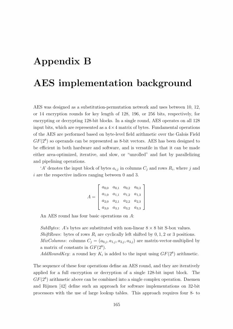
Appendix B
AES implementation background
AES was designed as a substitution-permutation network and uses between 10, 12,
or 14 encryption rounds for key length of 128, 196, or 256 bits, respectively, for
encrypting or decrypting 128-bit blocks. In a single round, AES operates on all 128
input bits, which are represented as a 4×4 matrix of bytes. Fundamental operations
of the AES are performed based on byte-level field arithmetic over the Galois Field
GF (28) so operands can be represented as 8-bit vectors. AES has been designed to
be efficient in both hardware and software, and is versatile in that it can be made
either area-optimized, iterative, and slow, or “unrolled” and fast by parallelizing
and pipelining operations.
‘A’ denotes the input block of bytes ai,j in columns Cj and rows Ri, where j and
i are the respective indices ranging between 0 and 3.
A =
a0,0 a0,1 a0,2 a0,3
a1,0 a1,1 a1,2 a1,3
a2,0 a2,1 a2,2 a2,3
a3,0 a3,1 a3,2 a3,3
An AES round has four basic operations on A:
SubBytes : A’s bytes are substituted with non-linear 8× 8 bit S-box values.
ShiftRows : bytes of rows Ri are cyclically left shifted by 0, 1, 2 or 3 positions.
MixColumns : columns Cj = (a0,j, a1,j, a2,j, a3,j) are matrix-vector-multiplied by
a matrix of constants in GF (28).
AddRoundKey : a round key Ki is added to the input using GF (28) arithmetic.
The sequence of these four operations define an AES round, and they are iteratively
applied for a full encryption or decryption of a single 128-bit input block. The
GF (28) arithmetic above can be combined into a single complex operation. Daemen
and Rijmen [42] define such an approach for software implementations on 32-bit
processors with the use of large lookup tables. This approach requires four 8- to
165

32-bit lookup tables for the four round transformations, each the size of 8-Kibit. We
can compute these transformation tables, Tk[0..3], in the following way:
T0[x] =
S[x]× 02
S[x]
S[x]
S[x]× 03
T1[x] =
S[x]× 03
S[x]× 02
S[x]
S[x]
T2[x] =
S[x]
S[x]× 03
S[x]× 02
S[x]
T3[x] =
S[x]
S[x]
S[x]× 03
S[x]× 02
where S[x] denotes a table lookup in the original 8 × 8 bit AES S-box (for a more
detailed description of this AES optimization see NIST’s FIPS-197 [139]). The last
round, however, is unique in that it omits the MixColumns operation, so requires
special consideration. There are two ways for computing the last round, either by
“reversing” the MixColumns operation from the output of a regular round by an-
other multiplication in GF (28), or creating dedicated “last round” T-tables, one per
regular T-table. Some implementers, such as Fischer and Drutarovsky [65], opted
for MixColumn elimination, which is done on-the-fly within the round function.
Besides requiring additional logic resources for the decryption, this approach may
decrease performance since the “reversing” logic may extend the the critical data-
path. For this reason, we decided to add dedicated tables for the last round allows
us to maintain the same datapath for all rounds and keep as many “computations”
within embedded elements of the FPGA; we denote these T-tables as T ′j . We can
now redefine all transformation steps of a single AES round as
Ej = Kr[j] ⊕ T0[a0,j]⊕ T1[a1,(j+1 mod 4)]⊕ T2[a2,(j+2 mod 4)]⊕ T3[a3,(j+3 mod 4)] (B.1)
where Kr[j] is a corresponding 32-bit “sub-key” and Ej denotes one of four encrypted
output columns of a full round. We now see that based on only four T-table lookups
and four XOR operations, a 32-bit column Ej can be computed. To obtain the result
of a full round, Equation (B.1) must be performed four times with all 16 bytes.
Input data to an AES encryption can be defined as four 32-bit column vectors
Cj = (a0,j, a1,j, a2,j, a3,j) with the output similarly formatted in column vectors.
According to Equation B.1, these input column vectors need to be split into indi-
vidual bytes since all bytes are required for the computation steps for different Ej.
For example, for column C0 = (a0,0, a1,0, a2,0, a3,0), the first byte a0,0 is part of the
computation of E0, the second byte a1,0 is used in E3, etc. Since fixed data paths
are preferable in hardware implementations, we have rearranged the operands of
166
the equation to align the bytes according to the input columns Cj when feeding
them to the T-table lookup. In this way, we can implement a unified data path for
computing all four Ej for a full AES round. Thus, Equation (B.1) becomes
E0 = Kr[0] ⊕ T0(a0,0)⊕ T1(a1,1)⊕ T2(a2,2)⊕ T3(a3,3) = (a′0,0, a
′1,0, a
′2,0, a
′3,0)
E1 = Kr[1] ⊕ T3(a3,0)⊕ T0(a0,1)⊕ T1(a1,2)⊕ T2(a2,3) = (a′0,1, a
′1,1, a
′2,1, a
′3,1)
E2 = Kr[2] ⊕ T2(a2,0)⊕ T3(a3,1)⊕ T0(a0,2)⊕ T1(a1,3) = (a′0,2, a
′1,2, a
′2,2, a
′3,2)
E3 = Kr[3] ⊕ T1(a1,0)⊕ T2(a2,1)⊕ T3(a3,2)⊕ T0(a0,3) = (a′0,3, a
′1,3, a
′2,3, a
′3,3)
where ai,j denotes an input byte, and a′i,j the corresponding output byte after the
round transformation. The datapath requires a look-up to all of the four T-tables
for the second operand of each XOR operation. For example, the XOR component
at the first position of the sequential operations E0 to E3 and thus requires the
lookups T0(a0,0), T3(a3,0), T2(a2,0) and T1(a1,0) (in this order) and the corresponding
round key Kr[j]. Though operations are aligned for the same input column now, it
becomes apparent that the bytes of the input column are not processed in canonical
order, i.e., bytes need to be swapped for each column Cj = (a0,j, a1,j, a2,j, a3,j) first
before being fed as input to the next AES round. The required byte transposition
is reflected in the following equations (note that the given transpositions are static
so that they can be efficiently hardwired):
C0 = (a′0,0, a
′3,0, a
′2,0, a
′1,0)
C1 = (a′1,1, a
′0,1, a
′3,1, a
′2,1)
C2 = (a′2,2, a
′1,2, a
′0,2, a
′3,2)
C3 = (a′3,3, a
′2,3, a
′1,3, a
′0,3)
(B.2)
B.1 Decryption
Encryptor and decryption can be supported with the same circuit by only swapping
the values of the transformation tables and re-arranging the input. As with Equa-
tion (B.1), decryption of columns Dj is governed by the following set of equations:
D0 = Kr[0] ⊕ I0(a0,0)⊕ I1(a1,3)⊕ I2(a2,2)⊕ I3(a3,1) = (a′0,0, a
′1,0, a
′2,0, a
′3,0)
D3 = Kr[3] ⊕ I3(a3,0)⊕ I0(a0,3)⊕ I1(a1,2)⊕ I2(a2,1) = (a′0,3, a
′1,3, a
′2,3, a
′3,3)
D2 = Kr[2] ⊕ I2(a2,0)⊕ I3(a3,3)⊕ I0(a0,2)⊕ I1(a1,1) = (a′0,2, a
′1,2, a
′2,2, a
′3,2)
D1 = Kr[1] ⊕ I1(a1,0)⊕ I2(a2,3)⊕ I3(a3,2)⊕ I0(a0,1) = (a′0,1, a
′1,1, a
′2,1, a
′3,1)
This requires the following inversion tables (I-Tables), where S−1 denotes the
inverse 8× 8 S-box for the AES decryption:
167

S-boxS-boxS-boxS-box
0
31
63
95
127
S-boxS-boxS-boxS-box
main AESkey
roundkey 1
roundkey 9
roundkey 10
roundconstant 0
roundconstant 10
32
32
32
Figure B.1: Key expansion block diagram for AES-128; from the main key, ten “roundkeys” are computed.
I0[x] =
S−1[x]× 0E
S−1[x]× 09
S−1[x]× 0D
S−1[x]× 0B
I1[x] =
S−1[x]× 0B
S−1[x]× 0E
S−1[x]× 09
S−1[x]× 0D
I2[x] =
S−1[x]× 0D
S−1[x]× 0B
S−1[x]× 0E
S−1[x]× 09
I3[x] =
S−1[x]× 09
S−1[x]× 0D
S−1[x]× 0B
S−1[x]× 0E
We can see that compared to encryption, the input to the decryption equations is
different at two positions for each decrypted column Dj. But instead of changing
the datapath from the encryption function, we can change the order in which the
columns Dj are computed so that instead of computing E0, E1, E2, E3 for encryption,
we determine the decryption output in the column sequence D0, D3, D2, D1.
B.2 Key expansion
The AES key expansion derives “sub-keys” Kr (10, 12 and 14 for AES-128, 192, and
256, respectively) from the main key, where r denotes the round number.
The AES-128 key expansion function is outlined in Figure B.1. The first opera-
tion of AES is a 128-bit XOR of the main key K0 with the 128-bit initial plaintext
block. During expansion, each subkey is treated as four individual 32-bit words
Kr[j] for j = 0 . . . 3. The first word Kr[0] of each round subkey is transformed us-
ing byte-wise rotations and mappings using the same non-linear AES S-boxes. The
words corresponding to the indices j = 1 . . . 3, are XOR’d with the previous subkey
words Kr[j − 1]⊕K(r−1)[j].
168
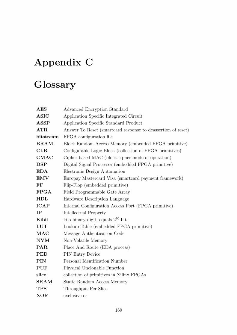
Appendix C
Glossary
AES Advanced Encryption Standard
ASIC Application Specific Integrated Circuit
ASSP Application Specific Standard Product
ATR Answer To Reset (smartcard response to deassertion of reset)
bitstream FPGA configuration file
BRAM Block Random Access Memory (embedded FPGA primitive)
CLB Configurable Logic Block (collection of FPGA primitives)
CMAC Cipher-based MAC (block cipher mode of operation)
DSP Digital Signal Processor (embedded FPGA primitive)
EDA Electronic Design Automation
EMV Europay Mastercard Visa (smartcard payment framework)
FF Flip-Flop (embedded primitive)
FPGA Field Programmable Gate Array
HDL Hardware Description Language
ICAP Internal Configuration Access Port (FPGA primitive)
IP Intellectual Property
Kibit kilo binary digit, equals 210 bits
LUT Lookup Table (embedded FPGA primitive)
MAC Message Authentication Code
NVM Non-Volatile Memory
PAR Place And Route (EDA process)
PED PIN Entry Device
PIN Personal Identification Number
PUF Physical Unclonable Function
slice collection of primitives in Xilinx FPGAs
SRAM Static Random Access Memory
TPS Throughput Per Slice
XOR exclusive or
169