Advanced and reliable GaAs/AlGaAs ICP-DRIE etching for ... · there is growing interest for DRIE...
9
Contents lists available at ScienceDirect Microelectronic Engineering journal homepage: www.elsevier.com/locate/mee Accelerated publication Advanced and reliable GaAs/AlGaAs ICP-DRIE etching for optoelectronic, microelectronic and microsystem applications P.B. Vigneron a , F. Joint a,b , N. Isac a , R. Colombelli a , E. Herth a, ⁎ a Centre de Nanosciences et de Nanotechnologies, CNRS UMR 9001, Univ. Paris-Sud, Université Paris-Saclay, C2N-Orsay, 91405 Orsay, Cedex, France b Observatoire de Paris, Laboratory for Studies of Radiation and Matter in Astrophysics (LERMA),75014 Paris, France ARTICLE INFO Keywords: Inductively coupled plasma Photoresist mask Plasma etching Surface morphology Smooth sidewalls High etch rate Selectivity ABSTRACT We investigate the parameter optimization for micron-scale etching by Inductive Coupled Plasma - Deep Reactive Ion Etching (ICP-DRIE) of GaAs/AlGaAs semiconductor heterostructures. Although dry etching ap- proaches have been reported in the literature using a broad variety of plasma etch tools, there is still need to meet the majority of microsystems dry etching requirements. The etch process family studied here, is dominated by the relative pressures of BCl 3 (Boron trichloride) and Cl 2 (Chlorine) gases. The influence of using a BCl 3 /Cl 2 / Ar/N 2 mixture at different pressures has been investigated: A small addition of N 2 (Nitrogen) is very effective inducing sidewall protection when using photoresist masks. The etch profile quality has been characterized as a function of the plasma process and of the etched feature sizes. The desired etch characteristics for GaAs/AlGaAs heterostructures can be achieved by controlling the various process parameters with good reliability, high se- lectivity, and – simultaneously – high etch rates and sidewall verticality. Etch rates from 1 to over 5.5 μm/min have been obtained. The selectivity with optical photoresist varies from 2.3 to 16. The presented results can be valuable for a wide range of applications involving fabrication of micro-electro-mechanical-systems or Micro Optoelectronic Mechanical Systems. 1. Introduction Current mainstream microelectronic and microsystem technology uses silicon as the substrate material [1–3]. III-V compound semi- conductors, on the other hand, dominate of course optoelectronic ap- plications [4–11]. However, III-V compound semiconductors suit high- performance applications even beyond optoelectronics, due to higher electron mobilities and peak velocities than silicon. As a consequence, there is growing interest for DRIE etching of III-V compound semi- conductors and ICP reactors have been widely used in both manu- facturing and research laboratories. The BCl 3 and Cl 2 -based chemistries are widely used in dry etching of III-V compound semiconductors. However, it is rare to use just Cl 2 or BCl 3 (or both together). Combinations with Ar or N 2 gases are generally employed [12–15], depending on the etched material system (GaAs, AlGaAs, GaP, GaSb and GaN) and also on the applications [16–23]. Sloped profiles may be necessary for some applications, such as a trenche, to guarantee adequate coverage during subsequent metal de- position. Vertical profiles (corresponding to an angle of 90 ± 2 ∘ ) are essential for etching mirror facets for semiconductor lasers, or a cavity in the substrate for MEMS devices. In particular, III-V compound semiconductors such as GaAs and AlGaAs are widely used for the mi- crofabrication of sensor devices for applications in optoelectronics, optical wireless communications [24,25] and microsystems [26]. The aforementioned applications demand anisotropic etch profiles, as well as smooth sidewalls and surface morphology, and high etch rates and selectivity. Conventional reactive ion etching (RIE) is often used for the selective etch process of III-V compounds [23]. However, RIE processes rely on only one RF chuck (called platen or bias power), making it difficult to achieve good etch uniformity on large wafers (100 mm wafers are nowadays commonly used in III-V technology). Moreover, elevated RF platen bias are typically necessary to achieve vertical sidewalls. This also leads to high etch rates, but the physical impact of the ions on the III-V compounds and on the mask is increased too. The former one can cause damage to the device [27–29]. The latter one reduces the mask selectivity. One solution is to use an ICP-DRIE reactor where two power inputs are employed for the plasma. One is the platen power, similar to a RIE reactor. The other is the ICP source power. The latter one plays the crucial role of ionizing and generating the plasma. This technology provides almost independent control of ion density and ion energy, respectively. With optimized ICP conditions, typically a low RF chuck power and a high ICP source power, minimum https://doi.org/10.1016/j.mee.2018.09.001 Received 3 August 2018; Accepted 11 September 2018 ⁎ Corresponding author. E-mail address: [email protected] (E. Herth). Microelectronic Engineering 202 (2018) 42–50 Available online 22 September 2018 0167-9317/ © 2018 Elsevier B.V. All rights reserved. T
Transcript of Advanced and reliable GaAs/AlGaAs ICP-DRIE etching for ... · there is growing interest for DRIE...
Contents lists available at ScienceDirect
Microelectronic Engineering
journal homepage: www.elsevier.com/locate/mee
Accelerated publication
Advanced and reliable GaAs/AlGaAs ICP-DRIE etching for optoelectronic,microelectronic and microsystem applications
P.B. Vignerona, F. Jointa,b, N. Isaca, R. Colombellia, E. Hertha,⁎
a Centre de Nanosciences et de Nanotechnologies, CNRS UMR 9001, Univ. Paris-Sud, Université Paris-Saclay, C2N-Orsay, 91405 Orsay, Cedex, FrancebObservatoire de Paris, Laboratory for Studies of Radiation and Matter in Astrophysics (LERMA),75014 Paris, France
A R T I C L E I N F O
Keywords:Inductively coupled plasmaPhotoresist maskPlasma etchingSurface morphologySmooth sidewallsHigh etch rateSelectivity
A B S T R A C T
We investigate the parameter optimization for micron-scale etching by Inductive Coupled Plasma - DeepReactive Ion Etching (ICP-DRIE) of GaAs/AlGaAs semiconductor heterostructures. Although dry etching ap-proaches have been reported in the literature using a broad variety of plasma etch tools, there is still need tomeet the majority of microsystems dry etching requirements. The etch process family studied here, is dominatedby the relative pressures of BCl3 (Boron trichloride) and Cl2 (Chlorine) gases. The influence of using a BCl3/Cl2/Ar/N2 mixture at different pressures has been investigated: A small addition of N2 (Nitrogen) is very effectiveinducing sidewall protection when using photoresist masks. The etch profile quality has been characterized as afunction of the plasma process and of the etched feature sizes. The desired etch characteristics for GaAs/AlGaAsheterostructures can be achieved by controlling the various process parameters with good reliability, high se-lectivity, and – simultaneously – high etch rates and sidewall verticality. Etch rates from 1 to over 5.5μm/minhave been obtained. The selectivity with optical photoresist varies from 2.3 to 16. The presented results can bevaluable for a wide range of applications involving fabrication of micro-electro-mechanical-systems or MicroOptoelectronic Mechanical Systems.
1. Introduction
Current mainstream microelectronic and microsystem technologyuses silicon as the substrate material [1–3]. III-V compound semi-conductors, on the other hand, dominate of course optoelectronic ap-plications [4–11]. However, III-V compound semiconductors suit high-performance applications even beyond optoelectronics, due to higherelectron mobilities and peak velocities than silicon. As a consequence,there is growing interest for DRIE etching of III-V compound semi-conductors and ICP reactors have been widely used in both manu-facturing and research laboratories.
The BCl3 and Cl2-based chemistries are widely used in dry etching ofIII-V compound semiconductors. However, it is rare to use just Cl2 orBCl3 (or both together). Combinations with Ar or N2 gases are generallyemployed [12–15], depending on the etched material system (GaAs,AlGaAs, GaP, GaSb and GaN) and also on the applications [16–23].Sloped profiles may be necessary for some applications, such as atrenche, to guarantee adequate coverage during subsequent metal de-position. Vertical profiles (corresponding to an angle of 90 ± 2∘) areessential for etching mirror facets for semiconductor lasers, or a cavityin the substrate for MEMS devices. In particular, III-V compound
semiconductors such as GaAs and AlGaAs are widely used for the mi-crofabrication of sensor devices for applications in optoelectronics,optical wireless communications [24,25] and microsystems [26].
The aforementioned applications demand anisotropic etch profiles,as well as smooth sidewalls and surface morphology, and high etchrates and selectivity. Conventional reactive ion etching (RIE) is oftenused for the selective etch process of III-V compounds [23]. However,RIE processes rely on only one RF chuck (called platen or bias power),making it difficult to achieve good etch uniformity on large wafers(100mm wafers are nowadays commonly used in III-V technology).Moreover, elevated RF platen bias are typically necessary to achievevertical sidewalls. This also leads to high etch rates, but the physicalimpact of the ions on the III-V compounds and on the mask is increasedtoo. The former one can cause damage to the device [27–29]. The latterone reduces the mask selectivity. One solution is to use an ICP-DRIEreactor where two power inputs are employed for the plasma. One isthe platen power, similar to a RIE reactor. The other is the ICP sourcepower. The latter one plays the crucial role of ionizing and generatingthe plasma. This technology provides almost independent control of iondensity and ion energy, respectively. With optimized ICP conditions,typically a low RF chuck power and a high ICP source power, minimum
https://doi.org/10.1016/j.mee.2018.09.001Received 3 August 2018; Accepted 11 September 2018
⁎ Corresponding author.E-mail address: [email protected] (E. Herth).
Microelectronic Engineering 202 (2018) 42–50
Available online 22 September 20180167-9317/ © 2018 Elsevier B.V. All rights reserved.
T
damage or damage-free etch with high etch rate and sidewalls can beobtained with III-V materials [15,30].
Several approaches to increase the etch selectivity have been de-veloped. The use of gases promoting formation of polymer films on thesurfaces was shown to favor the selectivity. In this article we show thata BCl3/Cl2/N2/Ar plasma chemistry can produce highly anisotropicetching of GaAs/AlGaAs heterostructures in combination with photo-resist-based masks. Each ICP-DRIE etching parameter has an effect onthe rate, anisotropy, surface roughness, and sidewall morphology. All ofthem must be carefully controlled for reliable device manufacturing.
Special attention has been paid to the problem of plasma-inducedstructural damages such as the micromasking and the sidewall rough-ness. Our objective is to optimize III-V compounds etching using a ICP-DRIE etcher. We have identified plasma conditions that provide notonly an adequate surface chemistry but vertical and smooth sidewalls aswell. The paper is organized as follows: section II describes the solutionto overcome the micromasking phenomenon and to obtain a smoothsurface using a photoresist mask (for low cost processing). Section IIIdescribes the ICP process for GaAs as a function of gas mixtures andpressures. In section IV, we investigate the sidewall quality and angle
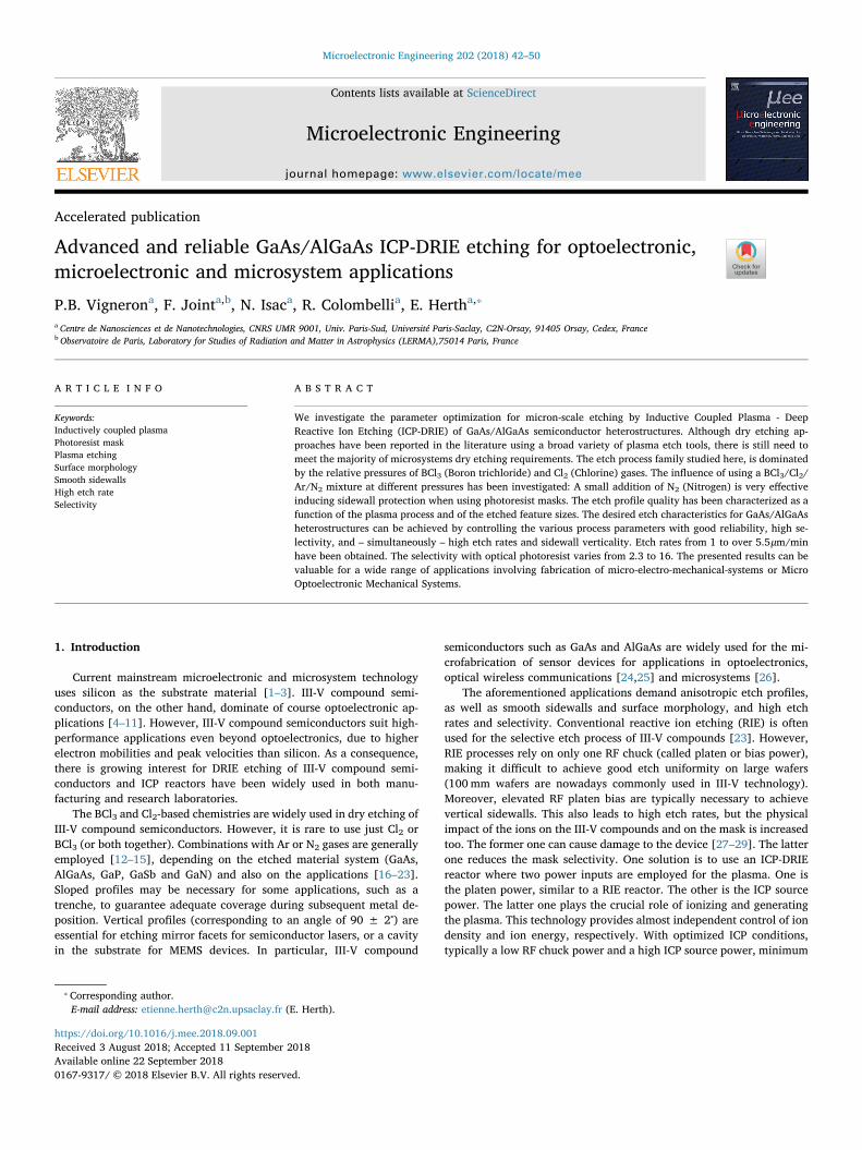
Fig. 1. SEM images of features etched into a GaAs wafer with micromasking effects apparent on the surface: a) with metal mask, b)-c) and d) with photoresist mask.
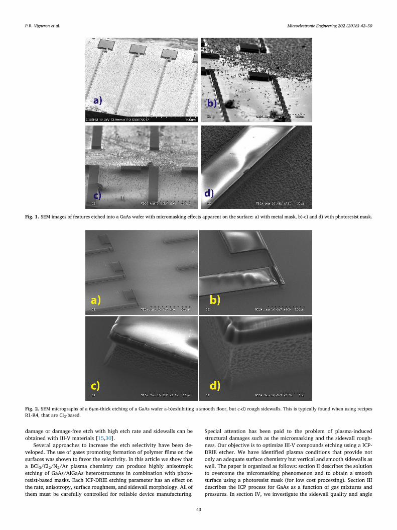
Fig. 2. SEM micrographs of a 6μm-thick etching of a GaAs wafer a-b)exhibiting a smooth floor, but c-d) rough sidewalls. This is typically found when using recipesR1-R4, that are Cl2-based.
P.B. Vigneron et al. Microelectronic Engineering 202 (2018) 42–50
43

profile by exploring how the shape of the photoresist mask evolvesduring the ICP processes. We conclude with a discussion of these resultsand their potentiel applications.
2. Experiment
The experiments were performed in a STS (Surface TechnologySystems) reactor, equipped with a maximum available power 900W,13.56MHz RF coil generator. The gases employed in this study wereBCl3, Cl2, Ar, N2 and O2. During all the experiments, the temperature ofthe electrode was fixed at 25∘C. A 5-min-long oxygen clean procedurewas performed between each run to remove any polymer from the re-actor sidewalls, minimize contamination, and preserve process repeat-ability. The samples were loaded into the reactor by mounting them onan alumina carrier wafer with silicone grease to ensure good thermalcontact. As part of the optimization of the etching parameters a maskdesign with different kinds of test structures (trenches and cavities) formeasuring the process outcome was employed. In this investigation asurface inspection of the etch result was the best way to check the etchcharacteristics. All test samples were 1 cm×1 cm pieces of bulk GaAsor GaAs /Al0.15Ga0.85As THz quantum cascade lasers [31].
We studied several different etch processes and their general char-acteristics were compared. Typical parameters from these processes aresummarized in Table I, with an etching time set at 5min for all thesamples. Photoresist (AZ9260, 6μm-thick), was patterned with testgeometries on GaAs wafers, or on GaAs /Al0.15Ga0.85As THz quantum
cascade heterostructures [31], and used as the mask material. The maskerosion was estimated by measuring its thickness pre- and post-etchingfor a fixed time. The mask selectivity was estimated by calculating theratio of the semiconductor etch rate to photoresist etch rate. Thesamples were etched and studied using an optical microscope and aScanning Electron Microscope (SEM). The latter one provides error onthe measurement due to the pixel size of the image. The error bars onthe depth and angle measurement, or on the etch rate and selectivityare plotted in all the figures.
3. Results
3.1. Micro-masking
Micro-masking occurs when material liberated during the etching isredeposited elsewhere on the sample and creates an undesirable addi-tional etch. It is most frequently encountered when a metal mask is usedbecause of the physical sputtering of small metal particles, that are notvolatile (as seen in Fig.1a). A photoresist mask may also induce polymerdeposition on the etched sidewalls due to a reaction with the plasmaand result in roughly etched surfaces due to micro-masking (as shownin Fig.1b, c and d). As a consequence, the micromasking phenomenacan significantly reduce the etch rate. Fig. 2 shows SEM images of thesamples after an etch with a Cl2-based chemistry. The samples presentvery smooth bottom surfaces. However an undercut is also observedand the sidewalls are rough. As predicted for Cl2-rich environments,
Fig. 3. SEM micrographs and corresponding optical photograph of features etched into GaAs with BCl3/Cl2/Ar. Typically found when using the recipes a) R1, b) R2 c)R3 and d)R4.
P.B. Vigneron et al. Microelectronic Engineering 202 (2018) 42–50
44
GaAs and AlGaAs were chemically etched causing severe undercut asobserved in Fig. 3, when using the recipes R1-R3. In BCl3-rich en-vironments instead, when using the recipe R4, GaAs and AlGaAs are ingeneral slightly passivated and the undercut effect is reduced[32,33,34]. Note: BCl3 may cause a problem because Boron-containingmolecules can be deposited onto the wafer surface. By adding Ar in theBCl3/Cl2 mixture, it is possible to sputter these non volatile productsaway. With the Ar in the BCl3/Cl2 mixture, we obtained less underetching (see Table 1: R4, R24, R25, R26 and R27). The effects of the gasmixture on the etch characteristics of GaAs show that by increasing theCl2 flow rate, the etched surface becomes very smooth, but the etchprofile is isotropic and the sidewalls are very rough. In the next section,the effect of plasma process parameters on the etch rate and the pho-toresist mask is studied.
3.2. High etch rate
The bulk micro-machining processes include wet etching, plasma(RIE or ICP DRIE) or both to realize microstructures. Because aniso-tropic wet etching often yields curved facets and rounded shapes, it isoften not suitable for optoelectronic applications [35,36]. As a con-sequence, the ICP-DRIE etching remains a very good alternative since itdoes not introduce undercut or rounded edges, and it is highly flexible.Shallow etch depths and lower etch rates are desirable for patternetching, whereas higher etch rates are preferred for very deep etching.Both these regimes can be attained with ICP-DRIE. A benchmark for theprocesses is an etch-rate greater or equal to 4μm/min for a GaAs
substrate.Our objective is to develop a recipe with increased etch rate by
facilitating the availability of chloride ions as a result of the reactionbetween BCl3 and Cl2. The addition of Ar or N2 to the BCl3/Cl2 mixtureaffects the etch rates. In essence, adding Ar or N2 can result in a dif-ferent degree of dissociation of Cl2. As shown in Table 2, the dissocia-tion enthalpy of the used gases are different: a balance in terms of in-jected gas flow ratio and the power used is required. We investigatedthe introduction of N2 to the BCl3/Cl2/ Ar mixture. It is important tonote that adding only a very small amount of N2 (2 or 5 sccm) alreadyresulted in a sizeable increase of the GaAs etching rate, as shown intable I. From these results, it is also observed that the etch rate increasesrapidly with increasing Cl2 flow rate in the ratio BCl3/Cl2 due to theincrease in the supply of reactive Cl+ or Cl species at the sample sur-face. The change in etch rates as a function of the Cl2 gas flow permitsto infer if the process is reactant or diffusion limited. On the other hand,at a fixed Cl2 flow, the etch rate increase with the BCl3 flow is not asdramatic. This stems from the higher dissociation energy of BCl3 mo-lecules that leads to a smaller number of available Cl radicals for thereaction.
The optimum conditions for obtaining a higher etch rate were ob-tained at a high concentration of N2 gas in the BCl3/Cl2/Ar mixture at10 mTorr (see Table I: R9, R10 and R11) and at even higher operatingpressures of 20–30 mTorr (see Table I: R20 and R21).
The addition of N2 to the BCl3/Cl2:Ar (6:5) mixture increased theGaAs etch rate. For example, the etch rate of GaAs increased from 2μm/min to 4μm/min with the addition of 3 sccm of N2. As shown in Fig. 4,the addition of N2 also enhances the sidewall passivation preventing theisotropic undercut (typical of Cl2-only based recipes) and produces avery anisotropic pattern transfer into the GaAs as well as into GaAs/AlGaAs heterostructures. We also observed that the etch rates of GaAsand of GaAs/AlGaAs heterostructures were not significantly different.As a matter of fact, the mechanisms for vertically etching bulk GaAs orGaAs/AlGaAs heterostructures are shown to be similar.
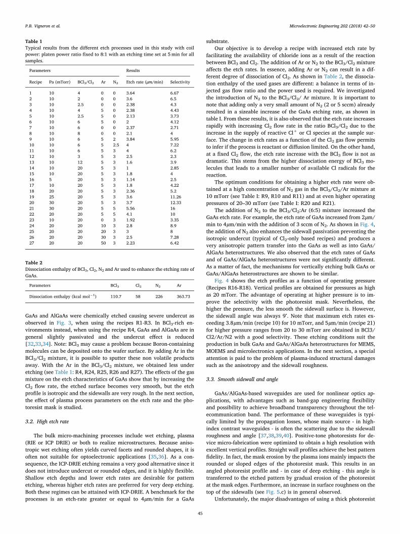
Fig. 4 shows the etch profiles as a function of operating pressure(Recipes R16-R18). Vertical profiles are obtained for pressures as highas 20 mTorr. The advantage of operating at higher pressure is to im-prove the selectivity with the photoresist mask. Nevertheless, thehigher the pressure, the less smooth the sidewall surface is. However,the sidewall angle was always 9∘. Note that maximum etch rates ex-ceeding 3.8μm/min (recipe 10) for 10 mTorr, and 5μm/min (recipe 21)for higher pressure ranges from 20 to 30 mTorr are obtained in BCl3/Cl2/Ar/N2 with a good selectivity. These etching conditions suit theproduction in bulk GaAs and GaAs/AlGaAs heterostructures for MEMS,MOEMS and microlectronics applications. In the next section, a specialattention is paid to the problem of plasma-induced structural damagessuch as the anisotropy and the sidewall roughness.
3.3. Smooth sidewall and angle
GaAs/AlGaAs-based waveguides are used for nonlinear optics ap-plications, with advantages such as band-gap engineering flexibilityand possibility to achieve broadband transparency throughout the tel-ecommunication band. The performance of these waveguides is typi-cally limited by the propagation losses, whose main source - in high-index contrast waveguides - is often the scattering due to the sidewallroughness and angle [37,38,39,40]. Positive-tone photoresists for de-vice micro-fabrication were optimized to obtain a high resolution withexcellent vertical profiles. Straight wall profiles achieve the best patternfidelity. In fact, the mask erosion by the plasma ions mainly impacts therounded or sloped edges of the photoresist mask. This results in anangled photoresist profile and - in case of deep etching - this angle istransferred to the etched pattern by gradual erosion of the photoresistat the mask edges. Furthermore, an increase in surface roughness on thetop of the sidewalls (see Fig. 5.c) is in general observed.
Unfortunately, the major disadvantages of using a thick photoresist
Table 1Typical results from the different etch processes used in this study with coilpower: platen power ratio fixed to 8:1 with an etching time set at 5min for allsamples.
Parameters Results
Recipe Pa (mTorr) BCl3/Cl2 Ar N2 Etch rate (μm/min) Selectivity
1 10 4 0 0 3.64 6.672 10 2 0 0 3.6 6.53 10 2.5 0 0 2.38 4.34 10 4 5 0 2.38 4.435 10 2.5 5 0 2.13 3.736 10 6 5 0 2 4.127 10 6 0 0 2.37 2.718 10 8 0 0 2.1 49 10 6 5 2 3.84 5.9510 10 6 5 2.5 4 7.2211 10 6 5 3 4 6.212 10 3 5 3 2.5 2.313 10 12 5 3 1.6 3.914 10 20 5 3 1 2.8515 10 20 5 3 1.8 416 5 20 5 3 1.14 2.517 10 20 5 3 1.8 4.2218 20 20 5 3 2.36 5.219 25 20 5 3 3.6 11.2620 30 20 5 3 3.7 12.3321 30 20 5 5 5.56 1622 20 20 5 5 4.1 1023 10 20 0 3 1.92 3.3524 20 20 10 3 2.8 8.925 20 20 20 3 3 826 20 20 30 3 2.5 7.2827 20 20 50 3 2.23 6.42
Table 2Dissociation enthalpy of BCl3, Cl2, N2 and Ar used to enhance the etching rate ofGaAs.
Parameters BCl3 Cl2 N2 Ar
Dissociation enthalpy (kcal mol−1) 110.7 58 226 363.73
P.B. Vigneron et al. Microelectronic Engineering 202 (2018) 42–50
45
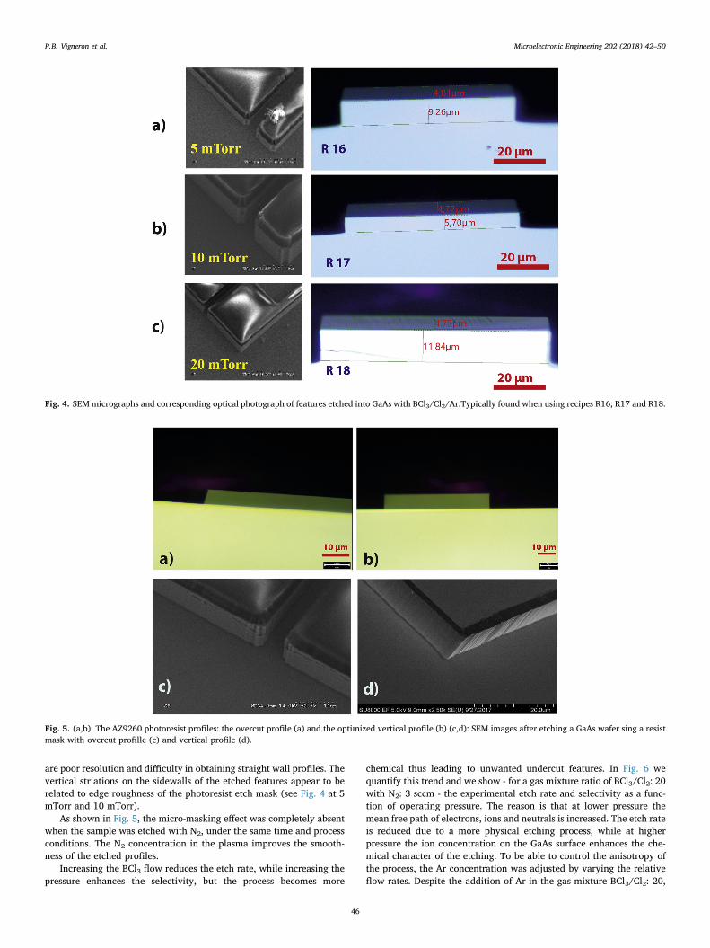
are poor resolution and difficulty in obtaining straight wall profiles. Thevertical striations on the sidewalls of the etched features appear to berelated to edge roughness of the photoresist etch mask (see Fig. 4 at 5mTorr and 10 mTorr).
As shown in Fig. 5, the micro-masking effect was completely absentwhen the sample was etched with N2, under the same time and processconditions. The N2 concentration in the plasma improves the smooth-ness of the etched profiles.
Increasing the BCl3 flow reduces the etch rate, while increasing thepressure enhances the selectivity, but the process becomes more
chemical thus leading to unwanted undercut features. In Fig. 6 wequantify this trend and we show - for a gas mixture ratio of BCl3/Cl2: 20with N2: 3 sccm - the experimental etch rate and selectivity as a func-tion of operating pressure. The reason is that at lower pressure themean free path of electrons, ions and neutrals is increased. The etch rateis reduced due to a more physical etching process, while at higherpressure the ion concentration on the GaAs surface enhances the che-mical character of the etching. To be able to control the anisotropy ofthe process, the Ar concentration was adjusted by varying the relativeflow rates. Despite the addition of Ar in the gas mixture BCl3/Cl2: 20,
Fig. 4. SEM micrographs and corresponding optical photograph of features etched into GaAs with BCl3/Cl2/Ar.Typically found when using recipes R16; R17 and R18.
Fig. 5. (a,b): The AZ9260 photoresist profiles: the overcut profile (a) and the optimized vertical profile (b) (c,d): SEM images after etching a GaAs wafer sing a resistmask with overcut profille (c) and vertical profile (d).
P.B. Vigneron et al. Microelectronic Engineering 202 (2018) 42–50
46
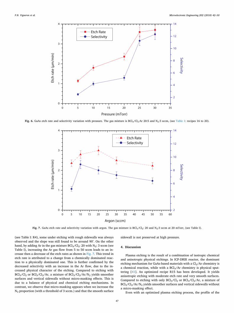
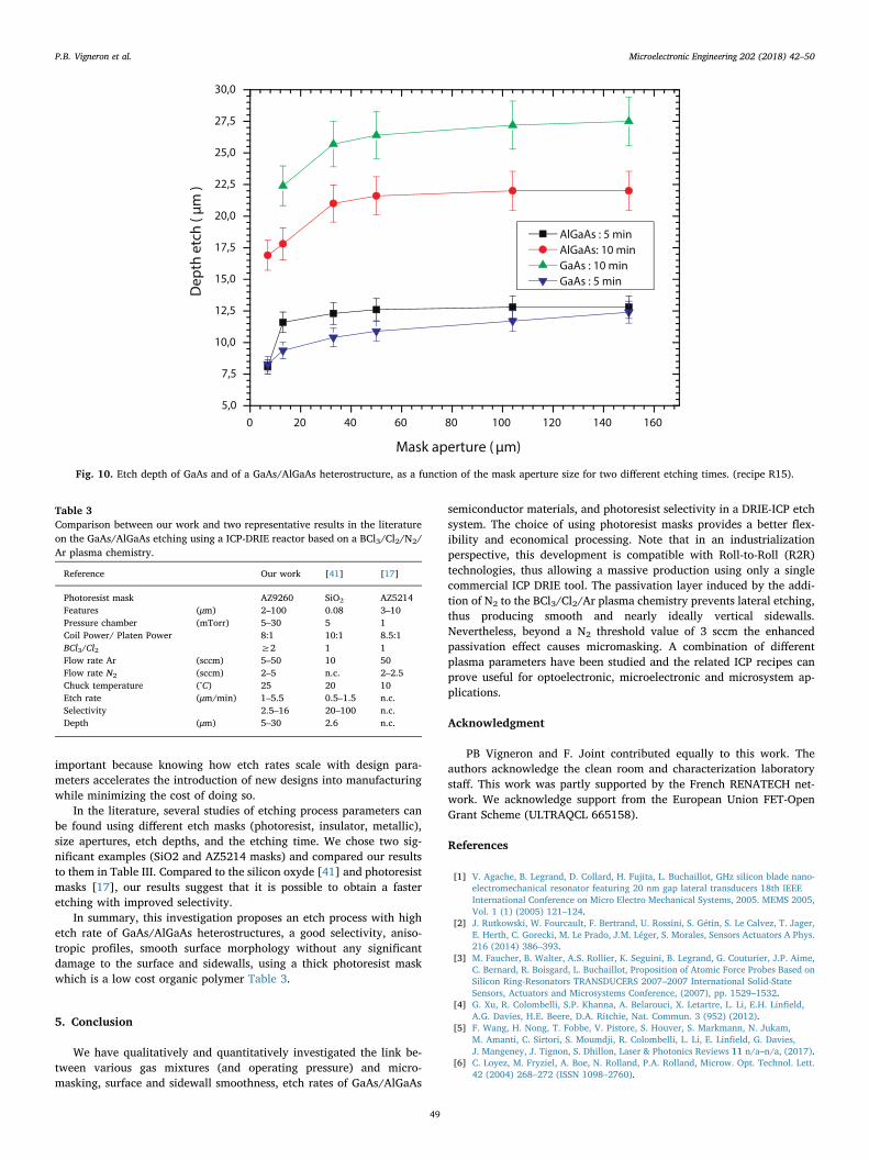
(see Table I: R4), some under etching with rough sidewalls was alwaysobserved and the slope was still found to be around 90∘. On the otherhand, by adding Ar in the gas mixture BCl3/Cl2: 20 with N2: 3 sccm (seeTable I), increasing the Ar gas flow from 5 to 50 sccm leads to an in-crease then a decrease of the etch rates as shown in Fig. 7. This trend inetch rate is attributed to a change from a chemically dominated reac-tion to a physically dominated one. This is further confirmed by thedecreased selectivity with an increase in the Ar flow, due to the in-creased physical character of the etching. Compared to etching withBCl3/Cl2 or BCl3/Cl2/Ar, a mixture of BCl3/Cl2/Ar/N2 yields smoothersurfaces and vertical sidewalls without micro-masking effects. This isdue to a balance of physical and chemical etching mechanisms. Incontrast, we observe that micro-masking appears when we increase theN2 proportion (with a threshold of 3 sccm.) and that the smooth surface
sidewall is not preserved at high pressure.
4. Discussion
Plasma etching is the result of a combination of isotropic chemicaland anisotropic physical etchings. In ICP-DRIE reactor, the dominantetching mechanism for GaAs-based materials with a Cl2/Ar chemistry isa chemical reaction, while with a BCl3/Ar chemistry is physical sput-tering [41]. An optimized recipe R15 has been developed. It yieldsanisotropic etching with moderate etch rate and very smooth surfaces.Compared to etching with only BCl3/Cl2 or BCl3/Cl2/Ar, a mixture ofBCl3/Cl2/Ar/N2 yields smoother surfaces and vertical sidewalls withouta micro-masking effect.
Even with an optimized plasma etching process, the profile of the
Fig. 6. GaAs etch rate and selectivity variation with pressure. The gas mixture is BCl3/Cl2:Ar 20:5 and N2:3 sccm, (see Table 1: recipes 16 to 20).
Fig. 7. GaAs etch rate and selectivity variation with argon. The gas mixture is BCl3/Cl2: 20 and N2:3 sccm at 20 mTorr, (see Table I).
P.B. Vigneron et al. Microelectronic Engineering 202 (2018) 42–50
47

photoresist sidewalls and the associated ripples are critical to manyapplications and do affect the quality of the etching. A vertical profilephotoresist provides the best pattern fidelity, but it is relatively difficultto obtain. The presence of the ripples depends on the pattern and alsoon the conditions of the lithographic process. It often occurs, especiallynear concave corners. The resist wall profile and the ripple effect can becontrolled by adjusting the photoresist, exposure dose, baking, devel-oper strength, and development time (see Fig. 8).
One of the significant issues in this etch is the ARDE (Aspect RatioDependent Etch). In fact, the scaling of the etch rate with the featuredimension is an important issue in the fabrication of microelectronic
and photonic devices. It requires a considerable effort to modify theetch processes each time changes in the design are made. As expected,as shown in Fig. 9, the GaAs etch rate depends on the mask openingsize. In particular, the smallest mask opening was etched the slowest.Moreover, as shown in Fig. 10, the etch rate of GaAs and AlGaAschanges significantly as a function of the processing time. Nevertheless,the quality of the sidewalls is similar in both cases. Since, as highlightedbefore, the mechanisms for etching vertically bulk GaAs and GaAs/Al-GaAs heterostructures are similar, the difference in selectivity betweenthe two is purely a result of the difference in the etch rates of thesemicondcutor material. The results reported in Fig.9a and Fig.10 are
Fig. 8. Ripple effects on GaAs etch rate: (a-b) optical view and (c-d) SEM view.
Fig. 9. ARDE effects: the GaAs etch rate is presented as a function of the mask aperture, a) for four different etching recipes (R11, R15, R21 and R22), b) illustrationof ARDE.
P.B. Vigneron et al. Microelectronic Engineering 202 (2018) 42–50
48
important because knowing how etch rates scale with design para-meters accelerates the introduction of new designs into manufacturingwhile minimizing the cost of doing so.
In the literature, several studies of etching process parameters canbe found using different etch masks (photoresist, insulator, metallic),size apertures, etch depths, and the etching time. We chose two sig-nificant examples (SiO2 and AZ5214 masks) and compared our resultsto them in Table III. Compared to the silicon oxyde [41] and photoresistmasks [17], our results suggest that it is possible to obtain a fasteretching with improved selectivity.
In summary, this investigation proposes an etch process with highetch rate of GaAs/AlGaAs heterostructures, a good selectivity, aniso-tropic profiles, smooth surface morphology without any significantdamage to the surface and sidewalls, using a thick photoresist maskwhich is a low cost organic polymer Table 3.
5. Conclusion
We have qualitatively and quantitatively investigated the link be-tween various gas mixtures (and operating pressure) and micro-masking, surface and sidewall smoothness, etch rates of GaAs/AlGaAs
semiconductor materials, and photoresist selectivity in a DRIE-ICP etchsystem. The choice of using photoresist masks provides a better flex-ibility and economical processing. Note that in an industrializationperspective, this development is compatible with Roll-to-Roll (R2R)technologies, thus allowing a massive production using only a singlecommercial ICP DRIE tool. The passivation layer induced by the addi-tion of N2 to the BCl3/Cl2/Ar plasma chemistry prevents lateral etching,thus producing smooth and nearly ideally vertical sidewalls.Nevertheless, beyond a N2 threshold value of 3 sccm the enhancedpassivation effect causes micromasking. A combination of differentplasma parameters have been studied and the related ICP recipes canprove useful for optoelectronic, microelectronic and microsystem ap-plications.
Acknowledgment
PB Vigneron and F. Joint contributed equally to this work. Theauthors acknowledge the clean room and characterization laboratorystaff. This work was partly supported by the French RENATECH net-work. We acknowledge support from the European Union FET-OpenGrant Scheme (ULTRAQCL 665158).
References
[1] V. Agache, B. Legrand, D. Collard, H. Fujita, L. Buchaillot, GHz silicon blade nano-electromechanical resonator featuring 20 nm gap lateral transducers 18th IEEEInternational Conference on Micro Electro Mechanical Systems, 2005. MEMS 2005,Vol. 1 (1) (2005) 121–124.
[2] J. Rutkowski, W. Fourcault, F. Bertrand, U. Rossini, S. Gétin, S. Le Calvez, T. Jager,E. Herth, C. Gorecki, M. Le Prado, J.M. Léger, S. Morales, Sensors Actuators A Phys.216 (2014) 386–393.
[3] M. Faucher, B. Walter, A.S. Rollier, K. Seguini, B. Legrand, G. Couturier, J.P. Aime,C. Bernard, R. Boisgard, L. Buchaillot, Proposition of Atomic Force Probes Based onSilicon Ring-Resonators TRANSDUCERS 2007–2007 International Solid-StateSensors, Actuators and Microsystems Conference, (2007), pp. 1529–1532.
[4] G. Xu, R. Colombelli, S.P. Khanna, A. Belarouci, X. Letartre, L. Li, E.H. Linfield,A.G. Davies, H.E. Beere, D.A. Ritchie, Nat. Commun. 3 (952) (2012).
[5] F. Wang, H. Nong, T. Fobbe, V. Pistore, S. Houver, S. Markmann, N. Jukam,M. Amanti, C. Sirtori, S. Moumdji, R. Colombelli, L. Li, E. Linfield, G. Davies,J. Mangeney, J. Tignon, S. Dhillon, Laser & Photonics Reviews 11 n/a–n/a, (2017).
[6] C. Loyez, M. Fryziel, A. Boe, N. Rolland, P.A. Rolland, Microw. Opt. Technol. Lett.42 (2004) 268–272 (ISSN 1098–2760).
Fig. 10. Etch depth of GaAs and of a GaAs/AlGaAs heterostructure, as a function of the mask aperture size for two different etching times. (recipe R15).
Table 3Comparison between our work and two representative results in the literatureon the GaAs/AlGaAs etching using a ICP-DRIE reactor based on a BCl3/Cl2/N2/Ar plasma chemistry.
Reference Our work [41] [17]
Photoresist mask AZ9260 SiO2 AZ5214Features (μm) 2–100 0.08 3–10Pressure chamber (mTorr) 5–30 5 1Coil Power/ Platen Power 8:1 10:1 8.5:1BCl3/Cl2 ≥2 1 1Flow rate Ar (sccm) 5–50 10 50Flow rate N2 (sccm) 2–5 n.c. 2–2.5Chuck temperature (∘C) 25 20 10Etch rate (μm/min) 1–5.5 0.5–1.5 n.c.Selectivity 2.5–16 20–100 n.c.Depth (μm) 5–30 2.6 n.c.
P.B. Vigneron et al. Microelectronic Engineering 202 (2018) 42–50
49

[7] M. Heddebaut, F. Elbahhar, C. Loyez, N. Obeid, N. Rolland, A. Rivenq,J.M. Rouvaen, Transportation Research Part C: Emerging Technologies 18 (2010)440–456.
[8] P. Lefevre, N. Haese, G. Lewandowski, C. Loyez, P.A. Rolland, E. Rogeaux,J.C. Sarkissian, A Full GaAs MMIC Phase-Locked Oscillator Using Sampling PhaseDetector and a Sampling Frequency Detector, 2000 30th European MicrowaveConference pp 1–4, 2000.
[9] D. Bajoni, E. Semenova, A. Lemaître, S. Bouchoule, E. Wertz, P. Senellart, S. Barbay,R. Kuszelewicz, J. Bloch, Phys. Rev. Lett. 101 (266402) (2008).
[10] D. Bajoni, E. Semenova, A. Lemaître, S. Bouchoule, E. Wertz, P. Senellart, J. Bloch,Phys. Rev. B 77 (2008) 113303, https://doi.org/10.1103/PhysRevB.77.113303.
[11] D. Bajoni, P. Senellart, E. Wertz, I. Sagnes, A. Miard, A. Lemaître, J. Bloch, Phys.Rev. Lett. 100 (047401) (2008).
[12] G. Franz, A. Kelp, P. Messerer, J. Vac. Sci. Technol. A 18 (2000) 2053–2061.[13] G. Franz, W. Hösler, R. Treichler, Journal of Vacuum Science & Technology B:
Microelectronics and Nanometer Structures Processing, Measurement, andPhenomena 19 (2001) 415–419.
[14] I.K. Baek, W.T. Lim, J.W. Lee, M.H. Jeon, G. Cho, S.J. S And Pearton, Journal ofVacuum Science & Technology B: Microelectronics and Nanometer StructuresProcessing, Measurement, and Phenomena 21 (2003) 2487–2491.
[15] L. Jalabert, P. Dubreuil, F. Carcenac, S. Pinaud, L. Salvagnac, H. Granier,C. Fontaine, Microelectron. Eng. 85 (2008) 1173–1178.
[16] Y.Z. Juang, Y.K. Su, S.C. Shei, B.C. Fang, J. Vac. Sci. Technol. A 12 (1994) 75–82(ISSN 0734-2101), 1520–8559.
[17] C. Constantine, Journal of Vacuum Science & Technology B: Microelectronics andNanometer Structures 13 (1995) 2025 (ISSN 0734211X).
[18] J.W. Lee, J. Hong, E.S. Lambers, C.R. Abernathy, S.J. Pearton, W.S. Hobson, F. Ren,Plasma Chem. Plasma Process. 17 (1997) 155–167 (ISSN 0272-43241572–8986).
[19] R.J. Shul, G.B. McClellan, R.D. Briggs, D.J. Rieger, S.J. Pearton, C.R. Abernathy,J.W. Lee, C. Constantine, C. Barratt, J. Vac. Sci. Technol. A 15 (1997) 633–637 ISSN0734-2101, 1520–8559.
[20] S. Agarwala, O. King, S. Horst, R. Wilson, D. Stone, M. Dagenais, Y.J. Chen, J. Vac.Sci. Technol. A 17 (1999) 52–55 ISSN 0734-2101, 1520–8559.
[21] M. Karlsson, F. Nikolajeff, Appl. Opt. 41 (902) (2002) 1539–4522.[22] T. Maeda, J.W. Lee, R.J. Shul, J. Han, J. Hong, E.S. Lambers, S.J. Pearton,
C.R. Abernathy, W.S. Hobson, Appl. Surf. Sci. 143 (1999) 174–182.[23] S.J. Pearton, U.K. Chakrabarti, W.S. Hobson, A.P. Kinsella, J. Vac. Sci. Technol. B 8
(1990) 607–617 (ISSN 0734-211X).[24] E. Herth, N. Rolland, T. Lasri, IEEE Antennas and Wireless Propagation Letters 9
(2010) 934–937.[25] E. Herth, S. Seok, N. Rolland, T. Lasri, Sensors Actuators A Phys. 173 (2012)
238–243.[26] V. Lacour, E. Herth, F. Lardet-Vieudrin, J.J. Dubowski, T. Leblois, Procedia
Engineering 120 (2015) 721–726.[27] S.J. Pearton, U.K. Chakrabarti, W.S. Hobson, J. Appl. Phys. 66 (1989) 2061–2064.[28] S.W. Pang, G.A. Lincoln, R.W. McClelland, P.D. Degraff, M.W. Geis, W.J. Piacentini,
J. Vac. Sci. Technol. B 1 (1983) 1334–1337 (ISSN 0734-211X).[29] G. Franz, J. Vac. Sci. Technol. A 19 (2001) 762–772.[30] A. Larrue, D. Belharet, P. Dubreuil, S. Bonnefont, O. Gauthier-Lafaye,
A. Monmayrant, F. Lozes-Dupuy, S. Moumdji, Journal of Vacuum Science &Technology B, Nanotechnology and Microelectronics 29 (2011) 021006.
[31] G. Xu, L. Li, N. Isac, Y. Halioua, A. Giles Davies, E.H. Linfield, R. Colombelli, Appl.Phys. Lett. 104 (2014) 091112.
[32] K.A. Atlasov, P. Gallo, A. Rudra, B. Dwir, E. Kapon, J. Vac. Sci. Technol. B 27 (2009)L21.
[33] Y. Chen, B.S. Ooi, G.I. Ng, C.L. Tan, Y.C. Chan, Dry plasma etching of GaAs viasusing BCl3/Ar and Cl2/Ar plasmas Design, Fabrication, and Characterization ofPhotonic Devices, International Society for Optics and Photonics, 3896 1999, pp.199–207.
[34] G.T. Edwards, A. Sobiesierski, D.I. Westwood, P.M. Smowton, Semicond. Sci.Technol. 22 (2007) 1010.
[35] Z.L. Zhang, N.C. MacDonald, J. Microelectromech. Syst. 2 (1993) 66–73.[36] A. Bienaime, C. Elie-Caille, T. Leblois, J. Nanosci. Nanotechnol. 12 (2012)
6855–6863.[37] J.S. Aitchison, D.C. Hutchings, J.U. Kang, G.I. Stegeman, A. Villeneuve, IEEE J.
Quantum Electron. 33 (1997) 341–348.[38] H.E.G. Arnot, H.P. Zappe, J.E. Epler, B. Graf, R. Widmer, H.W. Lehmann, Electron.
Lett. 29 (1993) 1131–1133.[39] J. Shin, Y.C. Chang, N. Dagli, Opt. Express 17 (2009) 3390–3395.[40] G.A. Porkolab, P. Apiratikul, B. Wang, S.H. Guo, C.J.K. Richardson, Opt. Express 22
(2014) 7733–7743.[41] M. Volatier, D. Duchesne, R. Morandotti, R. Arès, V. Aimez, Nanotechnology 21
(2010) 134,014.
P.B. Vigneron et al. Microelectronic Engineering 202 (2018) 42–50
50