
Advanced Accelerator Adapter - Electro-Mechanical ...
68
www.openpowerfoundation.org
Transcript of Advanced Accelerator Adapter - Electro-Mechanical ...

Advanced Accelerator Adapter November 8, 2017 Revision 1.0
OpenPOWER Foundation iiWorkgroup Specification
Standard Track
Advanced Accelerator Adapter: Electro-Mechanical Specification25G IO Interoperability Mode Work Group <[email protected]>OpenPower Foundation
Revision 1.0 (November 8, 2017)Copyright © 2017 OpenPOWER Foundation
All capitalized terms in the following text have the meanings assigned to them in the OpenPOWERIntellectual Property Rights Policy (the "OpenPOWER IPR Policy"). The full Policy may be found at theOpenPOWER website or are available upon request.
This document and translations of it may be copied and furnished to others, and derivative works thatcomment on or otherwise explain it or assist in its implementation may be prepared, copied, published,and distributed, in whole or in part, without restriction of any kind, provided that the above copyright noticeand this section are included on all such copies and derivative works. However, this document itself maynot be modified in any way, including by removing the copyright notice or references to OpenPOWER,except as needed for the purpose of developing any document or deliverable produced by an OpenPOW-ER Work Group (in which case the rules applicable to copyrights, as set forth in the OpenPOWER IPRPolicy, must be followed) or as required to translate it into languages other than English.
The limited permissions granted above are perpetual and will not be revoked by OpenPOWER or itssuccessors or assigns.
This document and the information contained herein is provided on an "AS IS" basis AND TO THEMAXIMUM EXTENT PERMITTED BY APPLICABLE LAW, THE OpenPOWER Foundation AS WELLAS THE AUTHORS AND DEVELOPERS OF THIS STANDARDS FINAL DELIVERABLE OR OTHERDOCUMENT HEREBY DISCLAIM ALL OTHER WARRANTIES AND CONDITIONS, EITHER EXPRESS,IMPLIED OR STATUTORY, INCLUDING BUT NOT LIMITED TO, ANY IMPLIED WARRANTIES, DUTIESOR CONDITIONS OF MERCHANTABILITY, OF FITNESS FOR A PARTICULAR PURPOSE, OFACCURACY OR COMPLETENESS OF RESPONSES, OF RESULTS, OF WORKMANLIKE EFFORT, OFLACK OF VIRUSES, OF LACK OF NEGLIGENCE OR NON-INFRINGEMENT.
OpenPOWER, the OpenPOWER logo, and openpowerfoundation.org are trademarks or registeredtrademarks of OpenPOWER Foundation, Inc., registered in many jurisdictions worldwide. Other company,product, and service names may be trademarks or service marks of others.
Abstract
This document defines an electro-mechanical specification for advanced accelerator adapters withinthe OpenPOWER eco-system supported by IBM® POWER9™. POWER9 modules present a 25Gbpsinterface organized into groups of 8 bit-lanes. Innovation within the community is encourgaged forsystems that support accelerated computing and the accelerator adapters needed to make heteroge-neous / accelerated computing solutions available to the market.
This document is a Standard Track, Workgroup Specification work product owned by the 25G IO Interop-erability Compatability Workgroup and handled in compliance with the requirements outlined in theOpenPOWER Foundation Work Group (WG) Process document. It was created using the DocumentDevelopment Guide version 1.1.0. Comments, questions, etc. can be submitted to the public mailing listfor this document at <[email protected]>.

Advanced Accelerator Adapter November 8, 2017 Revision 1.0
OpenPOWER Foundation iiiWorkgroup Specification
Standard Track
Table of ContentsPreface ......................................................................................................................................... vii
1. Conventions ...................................................................................................................... vii2. Document change history ................................................................................................ viii
1. Introduction ................................................................................................................................ 11.1. Scope .............................................................................................................................. 11.2. Conformance to this Specification ................................................................................... 1
I. Mezzanine Adapter Card ............................................................................................................ 22. System Mechanical Details ................................................................................................ 3
2.1. Mezzanine Card Connectors ................................................................................... 32.2. Adapter Mezzanine Card Outline ............................................................................ 42.3. Mezzanine Card Mechanical and Attachment Requirements ................................... 92.4. Operating conditions ............................................................................................. 112.5. Adapter Thermal Requirements ............................................................................. 13
3. System Electrical Details .................................................................................................. 153.1. Power Delivery Capability ..................................................................................... 153.2. Power Initialization Timing ..................................................................................... 153.3. Power Down Timing .............................................................................................. 163.4. Adapter device wiring for OpenCAPI 3.0 ............................................................... 173.5. Adapter Physical card diagram .............................................................................. 193.6. Connector 1 Pinout ............................................................................................... 203.7. Connector 2 Pinout ............................................................................................... 213.8. Sideband Signals .................................................................................................. 223.9. PCI-e Express Interface ........................................................................................ 23
II. Cabled Interface Extension ...................................................................................................... 244. Advanced Accelerator Adapter Cable Interface Guidelines ............................................... 25
4.1. Power9 Advanced Accelerator Cable Interface ...................................................... 254.2. Advanced Accelerator Cable ................................................................................. 30
III. 25 Gbit/sec Electrical Channel ................................................................................................ 385. Channel Overview ............................................................................................................ 39
5.1. High Level Description .......................................................................................... 395.2. Link Perspective .................................................................................................... 40
6. Channel Definition ............................................................................................................ 416.1. Channel requirements ........................................................................................... 416.2. Electrical Specifications ......................................................................................... 43
7. OIF CEI 28G Compliance ................................................................................................ 507.1. Approach ............................................................................................................... 507.2. Data Dependent Jitter (DDJ) measurement from CEI 28G SR ............................... 507.3. Endpoint compliance TX jitter models for channel simulation ................................. 517.4. Receiver Compliance ............................................................................................ 52
A. IBM® POWER9™ Specific Information .................................................................................... 53A.1. Global Parameters ........................................................................................................ 53A.2. IBM POWER9 Nominal Estimated Power Dissipation ................................................... 53A.3. POWER9 Transmitter ................................................................................................... 53A.4. POWER9 Receiver ....................................................................................................... 55A.5. Contacting IBM for Assistance ...................................................................................... 57
B. References .............................................................................................................................. 58B.1. OIF CEI 28Gbps SR Specification ................................................................................ 58
C. OpenPOWER Foundation overview ......................................................................................... 59

Advanced Accelerator Adapter November 8, 2017 Revision 1.0
OpenPOWER Foundation ivWorkgroup Specification
Standard Track
C.1. Foundation documentation ............................................................................................ 59C.2. Technical resources ...................................................................................................... 59C.3. Contact the foundation ................................................................................................. 60

Advanced Accelerator Adapter November 8, 2017 Revision 1.0
OpenPOWER Foundation vWorkgroup Specification
Standard Track
List of Figures2.1. Reference System Planar Connector (MEG-Array® 84740-102LF) .......................................... 42.2. Reference Mezzanine Card Plug connector (MEG-Array® 74221-101LF) ................................ 42.3. Top view of the reference mezzanine card outline with North direction indicator; dimensionsin millimeters .................................................................................................................................. 62.4. Bottom view of the reference mezzanine card with datum identification, connector place-ment and pin identification ............................................................................................................. 72.5. Mezzanine Card Height restriction .......................................................................................... 82.6. Mezzanine Card Envelope ...................................................................................................... 82.7. Reference Card Stiffener and Insulator Detail ......................................................................... 92.8. Bottom view ReferenceMezzanine Card with Stiffener ........................................................... 112.9. Allowable Heatsink Impedance .............................................................................................. 142.10. Impedance Area .................................................................................................................. 143.1. Mezzanine OP Card Power Initialization ............................................................................... 163.2. POWER 9 CPU OpenCAPI Lanes ........................................................................................ 173.3. Mezzanine Card Lane Identification ...................................................................................... 183.4. Mezzanine Card Physical Diagram ........................................................................................ 193.5. Connector 1 Pinout ............................................................................................................... 203.6. Connector 2 Pinout ............................................................................................................... 214.1. Mechanical Components of Advanced Accelerator Cable Interface ........................................ 254.2. Electrical Components of Advanced Accelerator Cable (AAC) Interface ................................. 254.3. Example of PCIe Carrier Card Stack-up ................................................................................ 264.4. PCIe Carrier Routing Topology .............................................................................................. 274.5. Internal Cable Connection ..................................................................................................... 304.6. Advanced Accelerator Cable Circuit Schematic ..................................................................... 314.7. Host Connector Pin Assignment ............................................................................................ 324.8. Carrier Connector Pin Assignment ........................................................................................ 334.9. Cable Assembly .................................................................................................................... 354.10. Internal Cable Construction ................................................................................................. 354.11. Connector Features ............................................................................................................. 364.12. 74 Pin Right Angle Receptacle + Straight Plug Solution ...................................................... 374.13. 74 Pin Vertical Receptacle + Right Angle Plug Solution ....................................................... 376.1. SDD11 and SDD22 differential return loss at C4(PADS) template for RX and TX. .................. 486.2. SDC11 and SCD11 for module input (TP1) and host input (TP4a) (for fb = 28 GHz) ............... 497.1. DDJ Measurement Method ................................................................................................... 51A.1. POWER9 TX SST termination picture excluding Tcoils and ESD affects added to the RXabove ........................................................................................................................................... 54A.2. POWER9 Rx termination picture excluding Tcoils and ESD affects. ...................................... 56A.3. POWER9 RX CTLE+LFEQ suite of curve in S parameter form ............................................. 57

Advanced Accelerator Adapter November 8, 2017 Revision 1.0
OpenPOWER Foundation viWorkgroup Specification
Standard Track
List of Tables2.1. Enviromental Specifications ................................................................................................... 122.2. Shock and Vibration Specification ......................................................................................... 122.3. Boundary Conditions ............................................................................................................. 133.1. System power delivery capability per add-in card (set of 2 connectors) ................................. 154.1. Loss Budget for AAC Interface .............................................................................................. 264.2. PCIe Carrier Routing Guidelines ........................................................................................... 274.3. Raw cable Characteristics ..................................................................................................... 346.1. Channel Requirements .......................................................................................................... 426.2. Specification for Reference Clock ......................................................................................... 436.3. Specification for CDR PLL .................................................................................................... 446.4. Electrical Spec: Tx and Rx Termination ................................................................................. 446.5. Endpoint Transmitter Electrical Output Specification. ............................................................. 456.6. Transmitter Output Jitter Specification for endpoint ( from CEI 28G SR ) ............................... 466.7. Endpoint Receiver Electrical Input Specification. ................................................................... 466.8. Endpoint Receiver Input Jitter Specification. .......................................................................... 46A.1. Global Parameters ................................................................................................................ 53A.2. Electrical Spec: POWER9Tx ................................................................................................. 53A.3. Rx Electrical Spec ................................................................................................................ 55

Advanced Accelerator Adapter November 8, 2017 Revision 1.0
OpenPOWER Foundation viiWorkgroup Specification
Standard Track
Preface1. ConventionsThe OpenPOWER Foundation documentation uses several typesetting conventions.
NoticesNotices take these forms:
Note
A handy tip or reminder.
Important
Something you must be aware of before proceeding.
Warning
Critical information about the risk of data loss or security issues.
ChangesAt certain points in the document lifecycle, knowing what changed in a document is important. Inthese situations, the following conventions will used.
• New text will appear like this. Text marked in this way is completely new.
• Deleted text will appear like this. Text marked in this way was removed from the previous versionand will not appear in the final, published document.
• Changed text will appear like this. Text marked in this way appeared in previous versions but hasbeen modified.
Command promptsIn general, examples use commands from the Linux operating system. Many of these are alsocommon with Mac OS, but may differ greatly from the Windows operating system equivalents.
For the Linux-based commands referenced, the following conventions will be followed:
$ prompt Any user, including the root user, can run commands that are prefixed with the $prompt.
# prompt The root user must run commands that are prefixed with the # prompt. You can alsoprefix these commands with the sudo command, if available, to run them.

Advanced Accelerator Adapter November 8, 2017 Revision 1.0
OpenPOWER Foundation viiiWorkgroup Specification
Standard Track
Document linksDocument links frequently appear throughout the documents. Generally, these links include a textfor the link, followed by a page number in parenthesis. For example, this link, Preface [vii],references the Preface chapter on page vii.
2. Document change historyThis version of the guide replaces and obsoletes all earlier versions.
The following table describes the most recent changes:
Revision Date Summary of Changes
November 8, 2017 • Version 1.0 - Final WG Specification
October 19, 2017 • (pre-8) Updates from Public Review• Modified mezzanine card section 2.1,2., and 2.3 to reflect a reference design and connector PN• Added abstract to point to the OIF spec and appropriate copyright languange
August 17, 2017 • Public Review Draft - approved by 25GIO WG
August 8, 2017 • (pre-7) Added section on Conformance, additional minor edits, removed Section 6.2 Mezzanine NetModel
August 2, 2017 • (pre-6) Updates to Table 5.1 about ILD, ILDB, and "moving average smoothing"
August 1, 2017 • (pre-5) Minor updated from workgroup review of pre-4
July 20, 2017 • (pre-4) Major update from workgroup review and comments
June 27, 2017 • (pre-3) Added part on cable extender version
April 27, 2017 • (pre-2) Updates from Dan Dreps review• Editorial updates from Jeff Brown review
March 13, 2017 • (pre-1) Creation of Electo-Mechanical consolidated specification. Merging 25gio content with themezzanine card content

Advanced Accelerator Adapter November 8, 2017 Revision 1.0
OpenPOWER Foundation 1Workgroup Specification
Standard Track
1. Introduction1.1. ScopeThis document defines an electro-mechanical specification for advanced accelerator adapterswithin the OpenPOWER eco-system supported by IBM® POWER9™. POWER9 modules presenta 25Gbps interface organized into groups of 8 bit-lanes. Innovation within the community is encour-gaged for systems that support accelerated computing and the accelerator adapters needed to makeheterogeneous / accelerated computing solutions available to the market.
This document defines two accelerator approaches. The first approach is a mezzanine cardattached to the system planar via two connectors. This approach is defined in Part I, “MezzanineAdapter Card” [2]. The second approach is via cable and is defined in Part II, “Cabled InterfaceExtension” [24]. While the accelerator card form factor is not defined in this specification Part II,“Cabled Interface Extension” [24] assumes a PCIe® card for illustration.
The electrical characteristics of the 25Gbps channel are defined in Part III, “25 Gbit/sec ElectricalChannel” [38].
1.2. Conformance to this SpecificationMezzanine adapter cards and systems designed to accept them must satisfy the requirementsdefined in Part I, “Mezzanine Adapter Card” [2].
Cabled adapter cards and systems designed to accept them must satisfy the requirements defined inPart II, “Cabled Interface Extension” [24].
Systems, adapter cards, and the chip/modules that provide the channel endpoints must satisfy therequirements defined in Part III, “25 Gbit/sec Electrical Channel” [38].

Part I. Mezzanine Adapter CardThis part describes the mezzanine adapter card for OpenPOWER systems based on thePOWER9™ processor. These adapter cards attach to the 25 gbit/sec interface native to thePOWER9 and plug into the mezzanine card connectors.
This specification describes the system level details required of mezzanine add-in cards. Thisspecification is constrained to the use of the tested and verified connector technology and IO assign-ments. It also includes an overview of the mechanical requirements including system level airflowand pressure drop requirements.

Advanced Accelerator Adapter November 8, 2017 Revision 1.0
OpenPOWER Foundation 3Workgroup Specification
Standard Track
2. System Mechanical Details
Table of Contents2.1. Mezzanine Card Connectors ................................................................................................... 32.2. Adapter Mezzanine Card Outline ............................................................................................ 42.3. Mezzanine Card Mechanical and Attachment Requirements ................................................... 92.4. Operating conditions ............................................................................................................. 112.5. Adapter Thermal Requirements ............................................................................................. 13
This section describes the mechanical constraints and details of designing the Advanced AcceleratorAdapter add in card.
2.1. Mezzanine Card ConnectorsAdapter add-in cards use high-speed array connectors as the electrical interface to the systemplanar. The connector is a 400 pin, 4mm stack height, high-speed interconnect. The referencesystem planar uses the plug connector (FCI PN 84740-102LF). The adapter add-in card is requiredto use a compatible receptacle connector. An example/reference connector known to be compati-ble and demonstrated in this application is FCI PN 74221-101LF (see Figure 2.1, “Reference SystemPlanar Connector (MEG-Array® 84740-102LF)” [4]. Each add-in card co-docks two connec-tors, one of which is primarily for high speed signals and the other for power and lower speedsignals. Co-docking these connectors drive the specific PCB tolerances described in Section 2.2,“Adapter Mezzanine Card Outline” [4] . The low nominal pin wipe in the connectors drivesspecific mechanical tolerances on the bottom side stiffener, detailed in Section 2.3, “MezzanineCard Mechanical and Attachment Requirements” [9] .

Advanced Accelerator Adapter November 8, 2017 Revision 1.0
OpenPOWER Foundation 4Workgroup Specification
Standard Track
Figure 2.1. Reference System Planar Connector (MEG-Array® 84740-102LF)
Figure 2.2. Reference Mezzanine Card Plug connector (MEG-Array® 74221-101LF)
2.2. Adapter Mezzanine Card OutlineThe top view of the mezzanine card outline is shown in Figure 2.3, “Top view of the referencemezzanine card outline with North direction indicator; dimensions in millimeters” [6] and abottom view of the mezzanine card is shown in Figure 2.4, “Bottom view of the reference mezzanine

Advanced Accelerator Adapter November 8, 2017 Revision 1.0
OpenPOWER Foundation 5Workgroup Specification
Standard Track
card with datum identification, connector placement and pin identification” [7] . The maximumadd-in card planar dimensions are 78mm x 140mm. For orientation in the system, the north sideof the card is identified on the drawing. Of particular note is the alignment hole tolerance. Twoalignment pins are used to orient the card within the system. The origin pin (south side) drives thealignment and docking of the card to the planar. This feature is critical for proper alignment of theadd-in card and the system planar. The north side alignment pin is used to provide angular alignmentand may be slotted on the card for hole positional tolerance.
The dimensions for mounting holes are depicted in Figure 2.3, “Top view of the reference mezzaninecard outline with North direction indicator; dimensions in millimeters” [6]. The alignment holesand pins A1 and K40 are depicted in Figure 2.3, “Top view of the reference mezzanine card outlinewith North direction indicator; dimensions in millimeters” [6]. The orientation and connectoridentification (1 and 2) is also defined in this view as well as the location of two copper groundingpads located between the connector pair. Additional details for add-in card grounding requirementsare detailed in Section 2.3, “Mezzanine Card Mechanical and Attachment Requirements” [9].The dimensions and tolerances for the connector pin holes and alignment holes are required to bereplicated to add-in cards in order to ensure proper co-docking.

Advanced Accelerator Adapter November 8, 2017 Revision 1.0
OpenPOWER Foundation 6Workgroup Specification
Standard Track
Figure 2.3. Top view of the reference mezzanine card outline with North directionindicator; dimensions in millimeters

Advanced Accelerator Adapter November 8, 2017 Revision 1.0
OpenPOWER Foundation 7Workgroup Specification
Standard Track
Figure 2.4. Bottom view of the reference mezzanine card with datumidentification, connector placement and pin identification

Advanced Accelerator Adapter November 8, 2017 Revision 1.0
OpenPOWER Foundation 8Workgroup Specification
Standard Track
Maximum component height on the top side of the card is approximately 66mm. The total height ofadapter cards must be less than 71.75mm. It is preferred that the card extend the full height (includ-ing the heat sink), or provide airflow blocking features. This is covered in the Section 2.5, “AdapterThermal Requirements” [13].
Figure 2.5. Mezzanine Card Height restriction
Figure 2.6. Mezzanine Card Envelope
Advanced Accelerator Adapter November 8, 2017 Revision 1.0
OpenPOWER Foundation 9Workgroup Specification
Standard Track
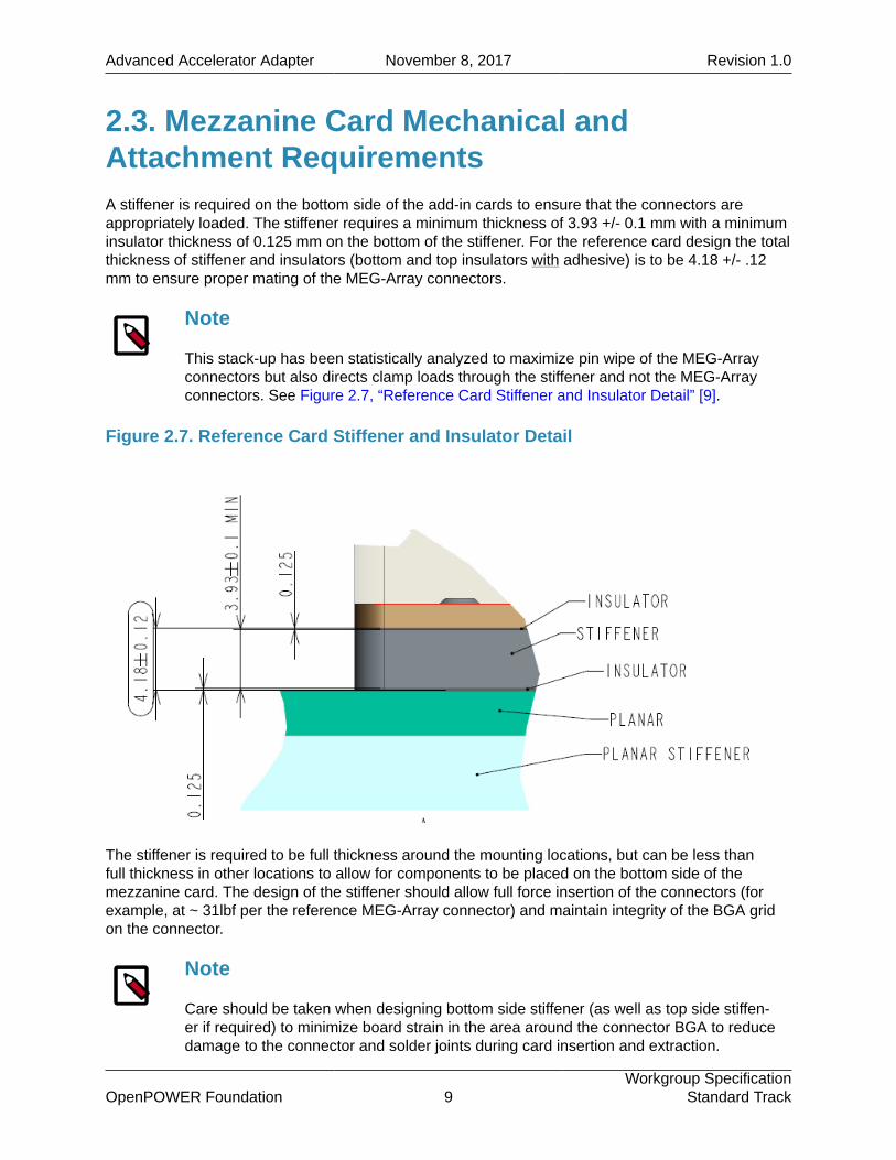
2.3. Mezzanine Card Mechanical andAttachment RequirementsA stiffener is required on the bottom side of the add-in cards to ensure that the connectors areappropriately loaded. The stiffener requires a minimum thickness of 3.93 +/- 0.1 mm with a minimuminsulator thickness of 0.125 mm on the bottom of the stiffener. For the reference card design the totalthickness of stiffener and insulators (bottom and top insulators with adhesive) is to be 4.18 +/- .12mm to ensure proper mating of the MEG-Array connectors.
Note
This stack-up has been statistically analyzed to maximize pin wipe of the MEG-Arrayconnectors but also directs clamp loads through the stiffener and not the MEG-Arrayconnectors. See Figure 2.7, “Reference Card Stiffener and Insulator Detail” [9].
Figure 2.7. Reference Card Stiffener and Insulator Detail
The stiffener is required to be full thickness around the mounting locations, but can be less thanfull thickness in other locations to allow for components to be placed on the bottom side of themezzanine card. The design of the stiffener should allow full force insertion of the connectors (forexample, at ~ 31lbf per the reference MEG-Array connector) and maintain integrity of the BGA gridon the connector.
Note
Care should be taken when designing bottom side stiffener (as well as top side stiffen-er if required) to minimize board strain in the area around the connector BGA to reducedamage to the connector and solder joints during card insertion and extraction.

Advanced Accelerator Adapter November 8, 2017 Revision 1.0
OpenPOWER Foundation 10Workgroup Specification
Standard Track
The stiffener is required to include two conductive fabric over foam gaskets to touch the coppergrounding pads dimensioned in Figure 2.3, “Top view of the reference mezzanine card outline withNorth direction indicator; dimensions in millimeters” [6]; Schlegel profile E1B with a nominalcompression of 0.265 mm is preferred (gasket attach plane would be nominally inset 0.35mm fromthe bottom stiffener plane to achieve this compression). This fabric over foam gaskets should alsoelectrically connect to the adapter card bottom stiffener and provide a ground path the card. This ischassis ground.
The System planar should have a package keep-out for the full 78 mm x 140 mm on the top side onthe main planar. However, top side traces are allowed in this region. Add-in cards must insure thatareas of the adapter card that are in contact with the main planar are electrically isolated (with theexception of the conductive foam gaskets). It is recommended that a thin insulator (.125mm) be usefor this purpose. Non-conductive coatings may be used, but may not be consider the primary methodof isolation and damage mitigation to the planar card.
Attachment to the planar is by 8 threaded fasteners at the mounting locations noted in figure 2 (andincluded in the appendix drawing). These 8 mounting locations are defined as M3 x 0.5 and thethreaded depth is 5 mm. accounting for a planar thickness of 3.01mm, the maximum threaded depthbeyond the bottom surface to the adapter card is 8mm. An exposed threaded fastener with a lengthbetween 6.5 and 7.5mm from bottom of the adapter card should be used.

Advanced Accelerator Adapter November 8, 2017 Revision 1.0
OpenPOWER Foundation 11Workgroup Specification
Standard Track
Figure 2.8. Bottom view ReferenceMezzanine Card with Stiffener
Removing the mezzanine card from the system planar requires an upward force to un-mate theconnectors.
2.4. Operating conditionsMechanical qualification (operational and non-operational) for adapter add-in cards should beperformed at a system level. The suggested environmental product specifications are presentedbelow for reference.
Advanced Accelerator Adapter November 8, 2017 Revision 1.0
OpenPOWER Foundation 12Workgroup Specification
Standard Track
2.4.1. Runtime Specification• Useful operational life of 5 years• Maximum of 8,760 power-on-hours per year (typical 8,640)• Nominal ambient input air temperature of 25C• Ambient temperature range of 5C to 40C• Relative humidity range of 8% to 85%• Air Quality is that of a typical business office (Class G1 & P1)• Altitude range of 0 to 3050 meters (see dry bulb temperature degrade table for details of max
altitude at given ambient temperature)• Nominal AC power input• Nominal usage of 100% during the power-on-hours for electronics• No preventive maintenance
2.4.2. Temperature, Humidity and AltitudeThis section defines the storage, shipping and operational atmospheric environmental limitationfor which the product should handle without physical and functional degradation. The systemunits should conform to these requirements in both horizontal and vertical configurations. Thesystem units should comply with the classifications detailed in Table 2.1, “Enviromental Specifica-tions” [12].
Table 2.1. Enviromental Specifications
ENVIROMENTAL CLASS Temperature (Dry Bulb) Altitude Relative Humidity
ASHRAE Class A3 Operating 5C - 40C
Up to 950 meters Uperlimit is derated 1Cfor ever 175 metersincrease in altitude
8% - 80%
Power - off 5C - 45C 5% - 80%
Storage -40C - 60C 5% - 100%
2.4.3. Shock and Vibration
Table 2.2. Shock and Vibration Specification
Item Test Specification Test Configuration Test Level Test Criteria
Packaging test Packaged SystemProducts, Testing forShipment, Test Levels,and Procedures.
Full-load system (withdesigned package)
Sine Sweep 0.5g for 30minutes all there axes
Random Vibration1.04grms all there axes
Drop test (drop 18 inchfor 6 faces)
Horizontal impact 1m/sall 4 sides
No physical andfunctional damage to thesystem unit.
Operational Vibration Vibration Levels forSystem Products;Product Environments,Product Classes.
Loaded in a rack System functional
Advanced Accelerator Adapter November 8, 2017 Revision 1.0
OpenPOWER Foundation 13Workgroup Specification
Standard Track
2.5. Adapter Thermal RequirementsThis thermal section will describe the minimum requirements for a single add-in card site, but isapplicable to multiple sites. Due to slight variance in the airflow within the system, the site with theminimum requirements will be described in this section.
The expected boundary condition for the adapter site is for airflow to enter the front (card south side)on the site and is exhausted toward the rear of the system (card north side). Airflow is not expectedto exit the boundary to the left or right and the mounted heatsink solution must ensure that a doesnot happen as it may interfere with the operation of the system.
Table 2.3, “Boundary Conditions” [13] summarizes the inlet and outlet conditions. Dependingon the system planar layout, the adapter site or sites could be directly behind the processors. Theslots must accept pre-heated air under the conditions for operation detailed in Table 2.3, “BoundaryConditions” [13].
Table 2.3. Boundary Conditions
Condition Average Temper-ature
Airflow Nominal Notes
Nominal 38C 30 CFM 25C room
Low Flow TBD 11 CFM Minimum flow expected in system
High Tempera-ture
50 C 50 CFM
Air flow distribution across the system is accomplished by managing the impedance of the proces-sor and the adapter heatsinks. It is important that the adapter card adheres to the impedancerequirements described in this section. In order to maintain proper airflow within the system,the cooling solution must restrict the flow such that all of the air passes through the heatsinkand does not provide an airflow bypass path above or around the heatsink. The total pressuredrop across the heatsink must include the entire area as outlined in Figure 2.10, “ImpedanceArea” [14]. The allowable range of heatsink impedance is shown in Figure 2.9, “AllowableHeatsink Impedance” [14], which outlines the upper and lower bounds of the heatsink impedance.The bounds help ensure adequate airflow balancing for all components that may go into the adapterslots.

Advanced Accelerator Adapter November 8, 2017 Revision 1.0
OpenPOWER Foundation 14Workgroup Specification
Standard Track
Figure 2.9. Allowable Heatsink Impedance
Figure 2.10. Impedance Area
Advanced Accelerator Adapter November 8, 2017 Revision 1.0
OpenPOWER Foundation 15Workgroup Specification
Standard Track
3. System Electrical Details
Table of Contents3.1. Power Delivery Capability ..................................................................................................... 153.2. Power Initialization Timing ..................................................................................................... 153.3. Power Down Timing .............................................................................................................. 163.4. Adapter device wiring for OpenCAPI 3.0 ............................................................................... 173.5. Adapter Physical card diagram ............................................................................................. 193.6. Connector 1 Pinout ............................................................................................................... 203.7. Connector 2 Pinout ............................................................................................................... 213.8. Sideband Signals .................................................................................................................. 223.9. PCI-e Express Interface ........................................................................................................ 23
This section details the power delivery capability and pinout of the connectors labeled 1 and 2in Figure 2.3, “Top view of the reference mezzanine card outline with North direction indicator;dimensions in millimeters” [6].
3.1. Power Delivery CapabilityTable 3.1, “System power delivery capability per add-in card (set of 2 connectors)” [15] details thetypical power delivery capability of the system as a function of voltage domain per add-in card. Allamperages are assumed to be equally distributed amongst all pins on that domain.
Table 3.1. System power delivery capability per add-in card (set of 2 connectors)
Voltage Domain Amperage Allowable Excursion
12 V 25 A 30% for <100ms
5 V 1 A 30% for <100ms
The system capacitance is 10uF for 5V without an inductor requirement.
The system capacitance is 10uF for 12V without an inductor requirement.
The capacitance recommendations for the adapter card are as follows:
• The maximum capacitance for 12V on the adapter card shall not exceed 1mF. (Required to meetthe power initialization timing requirements.)
• The maximum capacitance for 5V on the adapter card card shall not exceed 300uF.
3.2. Power Initialization TimingThe power initialization timing from the planar to the mezzanine card is detailed in Figure 3.1,“Mezzanine OP Card Power Initialization” [16]. As can be seen, 12V ramps to max over aduration of 20 to 100 ms, followed by a timeout of 1 to 2000 ms, after which 5V ramps to max overa duration of 1 to 20 ms. PWR_EN rises after 12V and 5V are stable typically 1 millisecond after T3shown in Figure 3.1, “Mezzanine OP Card Power Initialization” [16].

Advanced Accelerator Adapter November 8, 2017 Revision 1.0
OpenPOWER Foundation 16Workgroup Specification
Standard Track
Figure 3.1. Mezzanine OP Card Power Initialization
3.3. Power Down TimingThe adapter card is powered down by de-asserting the PWR_EN signal. The power rails from thesystem remain on during this time. If the system turns off the adapter device power, it is assumedthat the devices internal power rails stays powered on for 1 millisecond after PWR_EN de-assertion.

Advanced Accelerator Adapter November 8, 2017 Revision 1.0
OpenPOWER Foundation 17Workgroup Specification
Standard Track
3.4. Adapter device wiring for OpenCAPI 3.0Figure 3.2. POWER 9 CPU OpenCAPI Lanes
The above diagram illustrates one POWER9 CPU module. There are 32 available lanes forOpenCAPI use. The lanes are divided into four 8 Lane groups. This diagram also details the two 8lane groups that are not compatible with OpenCAPI.

Advanced Accelerator Adapter November 8, 2017 Revision 1.0
OpenPOWER Foundation 18Workgroup Specification
Standard Track
Figure 3.3. Mezzanine Card Lane Identification
The Mezzanine Card pinout is pre-defined and contains six 8-lane ports (OP0-OP5). These pinassignments are defined in Section 3.6, “Connector 1 Pinout” [20]. The implementation andassignment of the available ports is determined by the developer’s needs and requirements.
Potential use cases would be:
1. Developing the Mezzanine card for a pre-defined backplane. Care must be taken to ensure thatthe chosen ports and pin assignments of the Mezzanine card match the backplane wiring. Thechosen lanes must be attached to the valid OpenCAPI 3.0 lanes from the Power 9 planar.
2. Developing the Mezzanine card and the backplane. The developer has more freedom in thiscase to maximize the lane use and backplane wiring. The port use would be determined bythe developer’s application which would potentially factor in system planar component layout,number of CPU’s and wiring plane restrictions. The chosen lanes must attach to the validOpenCAPI 3.0 lanes from the selected Power 9 module.
Note
There are 6 lanes groups on the Mezzanine card and 4 lane groups from the Power 9.The developer’s use of each group is determined by their application.

Advanced Accelerator Adapter November 8, 2017 Revision 1.0
OpenPOWER Foundation 19Workgroup Specification
Standard Track
3.5. Adapter Physical card diagramFigure 3.4. Mezzanine Card Physical Diagram

Advanced Accelerator Adapter November 8, 2017 Revision 1.0
OpenPOWER Foundation 20Workgroup Specification
Standard Track
3.6. Connector 1 PinoutFigure 3.5, “Connector 1 Pinout” [20] details the pinout of connector 1 (see Figure 2.3, “Top viewof the reference mezzanine card outline with North direction indicator; dimensions in millimeters” [6]for placement definition).
Connector Directivity Example: OP3_RX7_N means that the receiver is on the OP card and thetransmitter is on the system planar, while OP3_TX7_N means that the transmitter is on the OP cardand the receiver is on the system planar.
The source spreadsheet for the Connector 1 pinout is available athttps://members.openpowerfoundation.org/document/dl/1159.
Figure 3.5. Connector 1 Pinout

Advanced Accelerator Adapter November 8, 2017 Revision 1.0
OpenPOWER Foundation 21Workgroup Specification
Standard Track
3.7. Connector 2 PinoutFigure 3.6, “Connector 2 Pinout” [21] details the pinout of connector 2 (see Figure 2.3, “Top viewof the reference mezzanine card outline with North direction indicator; dimensions in millimeters” [6]for placement definition).
Connector Directivity Example: OP3_RX7_N means that the receiver is on the OP card and thetransmitter is on the system planar, while OP3_TX7_N means that the transmitter is on the OP cardand the receiver is on the system planar.
The source spreadsheet for the Connector 2 pinout is available athttps://members.openpowerfoundation.org/document/dl/1159.
Figure 3.6. Connector 2 Pinout

Advanced Accelerator Adapter November 8, 2017 Revision 1.0
OpenPOWER Foundation 22Workgroup Specification
Standard Track
3.8. Sideband SignalsThe following are the sideband signals present:
REFCLK_100MHz PCIE reference clk. (from system logic)
REFCLK_133MHz 156.25MHz reference clk. From CPU. Can also be configured tobe 133MHz.
I2C_ADDR0/1 I2C bus address LSBs. Pulled high (1.8V only) or pulled low onmotherboard. These are used to set the physical address of theadapter device. These pins must be at a steady state voltagebefore the adapter device is taken out of reset.
SMB_CLK/DAT SMBUS. Only supports operation at 1.8V. Care must betaken that this signal does not activate before PWR_EN andPWR_GOOD is valid. It is recommended that this signal beANDED with PWR_EN at minimum since PWR_GOOD is optional
JTAG_SEL control signal into adapter device to enable JTAG debuginterface. 1.8V signal. Pulldown on motherboard for normaloperation. Pull high on Mezz. card for JTAG operation.
JTAG_TCK/TMS/TDI/TDO/TRST_N
JTAG interface for debug. Scan rings can span multiple risersites. Ring accessible through debug connector on motherboard.1.8V operation only.
PERST_N PERST signal to adapter device. Effectively is the master reset.1.8V level signal.
PWR_EN Master on/off switch to adapter device power subsystem. 1.8Vlevel signal only (OD, pullup is on motherboard). Signal isgenerated by logic on system planar and is controlled by powersequencer. This signal indicates to the adapter card that theadapter card power is enabled. The system asserts this signalto power on the module and shall be asserted only after all inputrails are stable.
PWR_BRAKE_N Power control signal to adapter device. 1.8V signal. OD. Pullupon motherboard. This signal may be used to indicate the adaptermay go into a lower power state potentially reducing clock ratesand power consumption. Use by system is optional.
PWR_GOOD Adapter device PGOOD signal to system. 1.8V OD. Pullup with10K on motherboard. Indicates to power sequencer that -adapterregs are good. Module power good. The module will assert thissignal when all its internal power regulators are stable. Use bysystem is optional.
TH_OVERT_N Emergency panic signal from the adapter device to the systemthat catastrophic thermal condition is imminent and device isgoing to shut down. 1.8V level signal to motherboard. Signals
Advanced Accelerator Adapter November 8, 2017 Revision 1.0
OpenPOWER Foundation 23Workgroup Specification
Standard Track
for each adapter device gathered together and fed to powersequencer. Care must be taken that this signal does not activatebefore PWR_EN and PWR_GOOD is valid. It is recommend-ed that this signal be ANDED with PWR_EN at minimum sincePWR_GOOD is optional and pulled up when not used.
INT_RST_N Reset to adapter device controlled by Processor I2C bus. Thissignal must have a pullup to 3.3V on the Mezzanine card.
PRSNT_1A/2A/1B/2B presence detect loop. Short PRSNT_1A to PRSNT_1B and shortPRSNT_2A to PRSNT_2B on adapter device. Motherboard usesthese to form a presence detect loop that is only true when thecard is fully and correctly seated. Signal is used by JTAG scanring bypass logic & pcie device prsnt detect logic
Note
1.8V and 3.3V levels imply +/- 10% inclusive of AC+DC variations.
3.9. PCI-e Express InterfaceEach Mezzanine card has a x2 PCI Express (PCIe) interface that can be used in many ways, withone being sideband support for configuration. Section 3.7, “Connector 2 Pinout” [21] shows thisinterface labeled as PE0. This interface is compliant with PCI Express base Specifications.

Part II. Cabled Interface ExtensionThis part describes the use of a cabled connection to an adapter card. It uses a PCIe™ card as anexample but the cabled extension does not require the adapter card be PCIe.
Advanced Accelerator Adapter November 8, 2017 Revision 1.0
OpenPOWER Foundation 25Workgroup Specification
Standard Track
4. Advanced Accelerator Adapter CableInterface Guidelines
Table of Contents4.1. Power9 Advanced Accelerator Cable Interface ...................................................................... 254.2. Advanced Accelerator Cable ................................................................................................. 30
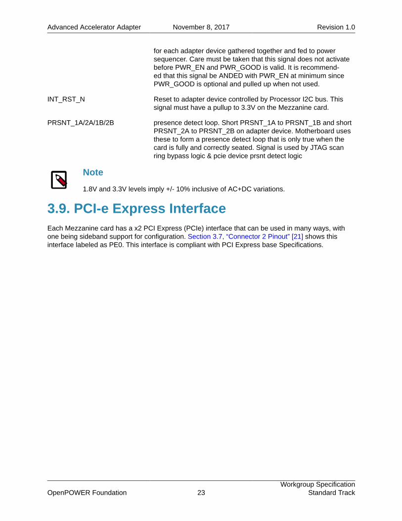
4.1. Power9 Advanced Accelerator CableInterfacePower9 platforms support the optional cabling of the 25 Gbit/s Advanced Accelerator Interface tothe advanced accelerator adapter in a riser card plugged into a PCIe slot in the same system. Inaddition, the adapter could be located in different drawer of the rack. This chapter contains informa-tion on topologies, connectivity, and routing guidelines for the advanced accelerator adapter cableinterface. Refer to Part I, “Mezzanine Adapter Card” [2] for the non-cabled version of the interface.
4.1.1. Advance Accelerated Cable (AAC) InterconnectionThe end-to-end AAC interconnection consists of the host board, the AAC cable, and the carrier cardas shown in Figure 4.1, “Mechanical Components of Advanced Accelerator Cable Interface” [25]
Figure 4.1. Mechanical Components of Advanced Accelerator Cable Interface
Figure 4.2. Electrical Components of Advanced Accelerator Cable (AAC) Interface
Advanced Accelerator Adapter November 8, 2017 Revision 1.0
OpenPOWER Foundation 26Workgroup Specification
Standard Track
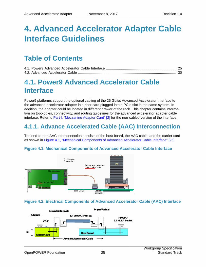
Table 4.1. Loss Budget for AAC Interface
Components Loss Budget (dB) Notes
CPU Socket 4.25 34 mm trace, LGA 7-2-7 laminate package
Host Planar Trace 3.8 2.2 inch Meg4, back-drilled via PCB
SlimSAS Cable Assembly 6.5 12.5 inch 30 AWG twin-ax cable and connectors
Carrier Card (PCIe) 3.5 3.0 inch Meg6, 0201 AC cap, blind via PCB
Advance Accelerator Socket 1.9 14mm trace, laminate package
Worst case PCB 0.9 Account for +/-10% PCB tolerance
Total 20.9 POWER9 receiver specification
4.1.2. PCIe Carrier Card Layout Guidelines
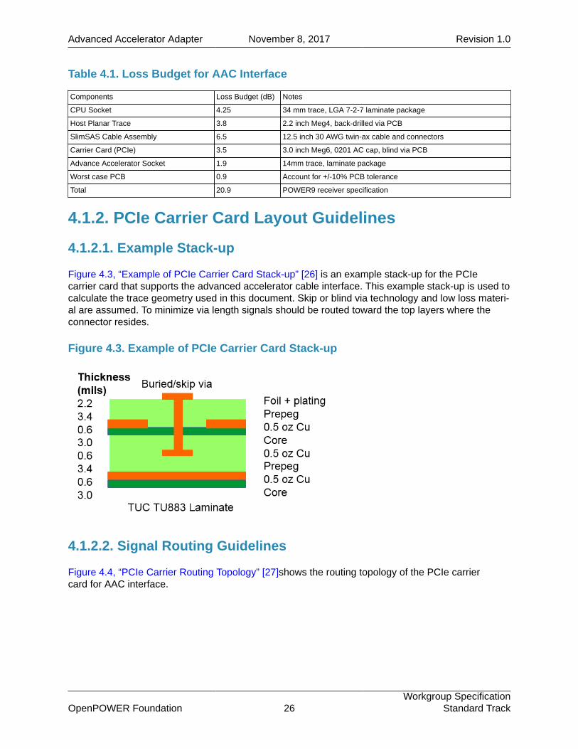
4.1.2.1. Example Stack-up
Figure 4.3, “Example of PCIe Carrier Card Stack-up” [26] is an example stack-up for the PCIecarrier card that supports the advanced accelerator cable interface. This example stack-up is used tocalculate the trace geometry used in this document. Skip or blind via technology and low loss materi-al are assumed. To minimize via length signals should be routed toward the top layers where theconnector resides.
Figure 4.3. Example of PCIe Carrier Card Stack-up
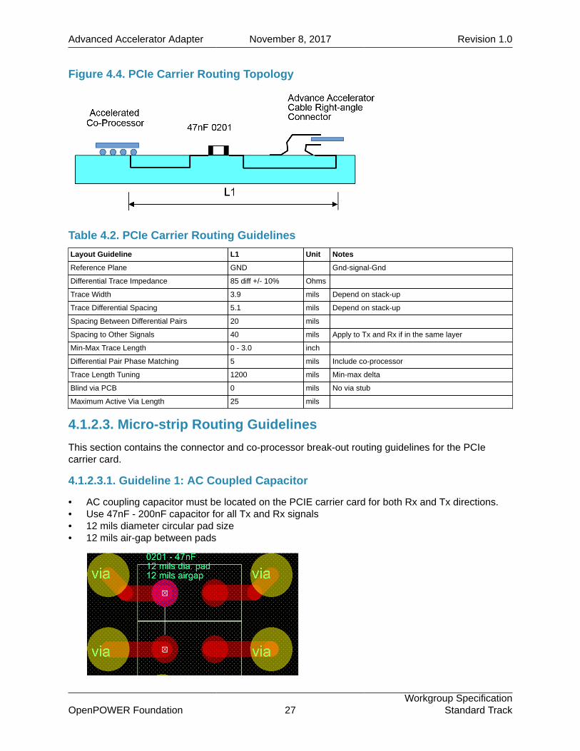
4.1.2.2. Signal Routing Guidelines
Figure 4.4, “PCIe Carrier Routing Topology” [27]shows the routing topology of the PCIe carriercard for AAC interface.
Advanced Accelerator Adapter November 8, 2017 Revision 1.0
OpenPOWER Foundation 27Workgroup Specification
Standard Track
Figure 4.4. PCIe Carrier Routing Topology
Table 4.2. PCIe Carrier Routing GuidelinesLayout Guideline L1 Unit Notes
Reference Plane GND Gnd-signal-Gnd
Differential Trace Impedance 85 diff +/- 10% Ohms
Trace Width 3.9 mils Depend on stack-up
Trace Differential Spacing 5.1 mils Depend on stack-up
Spacing Between Differential Pairs 20 mils
Spacing to Other Signals 40 mils Apply to Tx and Rx if in the same layer
Min-Max Trace Length 0 - 3.0 inch
Differential Pair Phase Matching 5 mils Include co-processor
Trace Length Tuning 1200 mils Min-max delta
Blind via PCB 0 mils No via stub
Maximum Active Via Length 25 mils
4.1.2.3. Micro-strip Routing GuidelinesThis section contains the connector and co-processor break-out routing guidelines for the PCIecarrier card.
4.1.2.3.1. Guideline 1: AC Coupled Capacitor
• AC coupling capacitor must be located on the PCIE carrier card for both Rx and Tx directions.• Use 47nF - 200nF capacitor for all Tx and Rx signals• 12 mils diameter circular pad size• 12 mils air-gap between pads

Advanced Accelerator Adapter November 8, 2017 Revision 1.0
OpenPOWER Foundation 28Workgroup Specification
Standard Track
4.1.2.3.2. Guideline 2: Signal Blind Via and Anti-pad
• Signal blind via pads must be voided (anti-pad) in the GND plane below. Minimum void size isequal to pad size in the constraint area of co-processor break-out, but it should be a regular anti-pad size in the open area.
• Avoid signal crossing blind via GND void• Prefer signal break-out in top and 1 stsignal layer for 1-layer-depth via to minimize active via
length• GND return via is required for each signal via, placed symmetrically 0.8 mm away• Differential via pitch in open-area = 20 mils• Via drill diameter = 10 mils• Via finish plated diameter = 8 mils• Via pad diameter = 15.7 mils• Via anti-pad in co-processor break-out area = 24x24 mils square• Via anti-pad in open area = 28x28 mils square
• Immediately match trace length at break-out to minimize serpentine compensation for phasematching rule in the open area. As shown as an example below: the before and after matchingreduces the phase tolerance from 12 mils to 1 mils.

Advanced Accelerator Adapter November 8, 2017 Revision 1.0
OpenPOWER Foundation 29Workgroup Specification
Standard Track
4.1.2.3.3. Guideline 3: 74-pin Connector Break-out
• Maximum micro-stripline length = 200 mils• Minimum micro-stripline spacing = 40 mils• Example of connector break-out
• Void GND reference plane below the signal pads, minimum void dimensions of 1x1.3mm asshown
• Avoid signals crossing connector anti-pad void
• Connect GND pads to common shape in the middle of the rows as shown

Advanced Accelerator Adapter November 8, 2017 Revision 1.0
OpenPOWER Foundation 30Workgroup Specification
Standard Track
• Smooth out the bending wire through out the design
4.2. Advanced Accelerator CableThe advanced accelerator cable connecting the host board to the PCIe carrier card is shown inFigure 4.5, “Internal Cable Connection” [30]. The right angle 74-pin connector should be used andplaced at the end of the PCIe card toward the CPU side. If the 74-pin vertical connector is selected,interference with the neighboring PCIe card may result.
Figure 4.5. Internal Cable Connection

Advanced Accelerator Adapter November 8, 2017 Revision 1.0
OpenPOWER Foundation 31Workgroup Specification
Standard Track
Figure 4.6. Advanced Accelerator Cable Circuit Schematic
I2C (SCL/SDA) and INT/RST voltage level is 3.3V +/- 10%
Cable_Pre_Det must have a 49.9 ohm pull-down to GND resistor located on the adapter card.
4.2.1. Cable/Connector Pin MappingThe interconnect allows lane and polarity reversal. Pin swapping is not allowed. Host connector pinordering and list are shown in Figure 4.7, “Host Connector Pin Assignment” [32]. Carrier connec-tor pin ordering and list are shown in Figure 4.8, “Carrier Connector Pin Assignment” [33].
The source spreadsheet for the connector pinouts is available athttps://members.openpowerfoundation.org/document/dl/1424.
Note: the pinout of the two connectors has been chosen such that a single twinax cable design canbe used for both connections in a differential pair / lane.

Advanced Accelerator Adapter November 8, 2017 Revision 1.0
OpenPOWER Foundation 32Workgroup Specification
Standard Track
Figure 4.7. Host Connector Pin Assignment

Advanced Accelerator Adapter November 8, 2017 Revision 1.0
OpenPOWER Foundation 33Workgroup Specification
Standard Track
Figure 4.8. Carrier Connector Pin Assignment

Advanced Accelerator Adapter November 8, 2017 Revision 1.0
OpenPOWER Foundation 34Workgroup Specification
Standard Track
4.2.2. Reference Advanced Accelerator Cable SolutionMechanical DescriptionThis section contains information about a reference solution that has been used to implement thisspecification.
The following Amphenol® part numbers represent a family of connectors, connector hardware, andcables that may be used as a reference solution.
Reference Part Numbers
Cable Assembly RSL74-0540-X X
Vertical 74-pin Connector U10-K274-26X X
Rigt Angle 74-pin Connector U10-J074-24X X
Table 4.3, “Raw cable Characteristics” [34] describes the physical and electrical characteristics ofthe reference cable.
Table 4.3. Raw cable Characteristics
Shielded Parallel Pair30 AWG (0.25mm) Solid Silver Plated Copper0.66mm Nom Fluorinated Polymer, Green Tint, Parallel Pair0.0254mm Aluminized Polyester, Foil In, Yellow Clear Polyester, HeatSealed
ConformanceRoHS CompliantAWM Style 22018 30V 80C VW-1
ElectricalAWG: 30Impedance: 85 Ohm +/- 5 OhmDesign: 23 GHzSDD21 (Maximum, 3M Sample)
6.71 dB/M @ 12.89 GHz7.04 dB/M @ 14.025 GHz8.47 dB/M @ 19.00 GHz
Figure 4.9, “Cable Assembly” [35] shows a drawing of the reference cable assembly.

Advanced Accelerator Adapter November 8, 2017 Revision 1.0
OpenPOWER Foundation 35Workgroup Specification
Standard Track
Figure 4.9. Cable Assembly
Figure 4.10, “Internal Cable Construction” [35] shows how the cable internal connections areconstructed.
Figure 4.10. Internal Cable Construction

Advanced Accelerator Adapter November 8, 2017 Revision 1.0
OpenPOWER Foundation 36Workgroup Specification
Standard Track
Figure 4.11, “Connector Features” [36] shows the various connector features. A specific cable /connector solution can be created from them. Figure 4.12, “74 Pin Right Angle Receptacle +Straight Plug Solution” [37] and Figure 4.13, “74 Pin Vertical Receptacle + Right Angle PlugSolution” [37] show two examples.
Figure 4.11. Connector Features

Advanced Accelerator Adapter November 8, 2017 Revision 1.0
OpenPOWER Foundation 37Workgroup Specification
Standard Track
Figure 4.12. 74 Pin Right Angle Receptacle + Straight Plug Solution
Figure 4.13. 74 Pin Vertical Receptacle + Right Angle Plug Solution

Part III. 25 Gbit/sec Electrical ChannelThis part describes the electrical interface specification for the 25 gbit/sec interface provided by theIBM® POWER9™ processor for POWER9 based OpenPOWER systems. It defines all requirementsto allow electrical signaling compatibility with the 25 Gbit/sec ports on the POWER9 microproces-sor module. This part identifies requirements on the endpoint PHY and the channel characteristics toensure electrical compatability.
The endpoint PHY is required to be compatible with the Optical Internetworking Forum (OIF) CEI28Gbps SR Specification. See Section B.1, “OIF CEI 28Gbps SR Specification” [58].
If the endpoint PHY is compatible with that specification all the compliance work done to provecompatability applies and the endpoint will interoperate with POWER9.
Details of the POWER9 PHY are provided in Appendix A, IBM® POWER9™ Specific Informa-tion [53] as a reference for the creation of accurate channel models.
This document will focus on the endpoint PHY specifications. Training will be covered in separatedocument.

Advanced Accelerator Adapter November 8, 2017 Revision 1.0
OpenPOWER Foundation 39Workgroup Specification
Standard Track
5. Channel Overview
Table of Contents5.1. High Level Description .......................................................................................................... 395.2. Link Perspective .................................................................................................................... 40
5.1. High Level DescriptionThe POWER9 25Gigabit port is a short channel chip-to-chip differential interface to provide datalinks between the POWER9 CPU and various specialized components. For example:
• CPU <=> CPU• CPU <=> GPU• CPU <=> FPGA• CPU <=> NIC
The port / channel design also allows cabled connections. The interface is a striped serial designwhere each lane is required to perform Clock Data Recovery (CDR) and there is no clock-forward-ing.
• Short reach chip-to-chip interface.
– -21 dB insertion loss at Nyquist
○ OIF CEI 28G SR allows 15dB module pin to module pin with module loss allocation of2(3dB). All 25G power designs close at -21dB C4-C4 to allow margin.
– Bit Error Rate per lane = 1E-15– ~7 inches of Main planar PCB wiring using Mg6– Up to 2 meters with half-active electrical cabling and ~6 inches of MG6 per end.– Up to 3 meters with full-active electrical cabling and ~6 inches of MG6 per end.– Active optical cables– Active Copper cables
• IO Protocol
– 25.78125Gbit, one speed no negotiation– Differential signaling with termination.– NRZ– Scrambled– DC or externally AC coupled. (AC coupling is externally located on the add-in card for TX
and RX.)
• Link Configuration: Unidirectional lanes Upstream and Downstream at equal widths.
• Reference clock: External 156.25 MHz crystal clock distributed on-PCB
The reference clock is always common and forwarded to the endpoint with the possibility ofcommon spread.

Advanced Accelerator Adapter November 8, 2017 Revision 1.0
OpenPOWER Foundation 40Workgroup Specification
Standard Track
In a multi-planar configuration (for example: drawer to drawer) the reference clock is forwarded.Thus making it a common reference clock design as required for OIF CEI compatibility.
5.2. Link PerspectiveThe channel is constructed from the endpoint PHY, the module package/substrate wiring and C4, thecard/planar wiring, connectors, and the Power9 module package/substrate wiring, C4, and socket.From a system perspective the channel is used to establish a communication link between theendpoint logic functions and the Power9 logic functions. This part of the electro-mechanical specifi-cation does not concern itself with the following link level information.
Link Power StatesLink Power States are defined in link specification.
Power-up SequenceThe PHY requires a sequence of events in order to power-up properly for operation. The power-upsequence of the voltage rails is defined in the electromechanical section. See Section 3.2, “PowerInitialization Timing” [15].
Training sequenceThe OIE CEI 28G SR specfication defines a "thin" PHY which does not include "thick" PHY functionssuch as: bit-lane repair, deskew, scrambler/descramble, etc. In addition to the "thick" PHY functions,the Link Layer is responsible for the CRC insertion/checking, replay buffers, and link layer retryprotocols.
Datalink Layer (DL) and Transaction Layer (TL) layermaterials.This design invokes 64/66 coding and scrambling and framing which are defined in the link specifica-tion.
Note
Details about the use of this PHY and channel for OpenCAPI may be found in theOpenCAPI DL Specification

Advanced Accelerator Adapter November 8, 2017 Revision 1.0
OpenPOWER Foundation 41Workgroup Specification
Standard Track
6. Channel Definition
Table of Contents6.1. Channel requirements ........................................................................................................... 416.2. Electrical Specifications ......................................................................................................... 43
6.1. Channel requirementsThe channel is a description of the end-end link. It consists of C4 bump pads, package includingballs, LGA modules, PCB route, connectors, sockets and other such physical media between thedriver and receiver. It does not include on-die termination.
This document defines a frequency domain compliance approach (see Chapter 7, “OIF CEI 28GCompliance” [50]) that specifies different combinations of frequency domain boundary conditionsfor compliant channels with the I/O properties defined in this document.
Following the channel compliance criteria of OIF CEI 28G SR will result in acceptable performance.
Note
Complementing the OIF CEI 28G SR compliance criteria with end to end timedomain simulation with POWER9 root complex and eco-system endpoints is stronglyrecommended.
Reference channel models are available at: https://members.openpowerfoundation.org/document/dl/455.
S-Parms are available at: https://members.openpowerfoundation.org/document/dl/455.
IBM Engineering support is available. See Section A.5, “Contacting IBM forAssistance” [57].

Advanced Accelerator Adapter November 8, 2017 Revision 1.0
OpenPOWER Foundation 42Workgroup Specification
Standard Track
Table 6.1. Channel Requirements
Symbol Parameter Min Typ Max Unit Notes
TCH_SKEW Delay difference between lanes withina bundle when FPGA is driving toPOWER9
132 UI Skew between lanes inclusive of on chip consump-tion (maximum skew of TX is 64UI from endpointinputers)
TCH_SKEW Delay difference between lanes withina bundle driven from POWER9,Launch skew, board and packageskew and retime skew
10 UI Skew between lanes inclusive with 1.5UI allocatedto cables
IL(f) Channel insertion loss at Nyquist 21 dB Includes PCB manufacturing variations andtolerances including effects of humidity/temperaturevariations on dielectric materials. Ball to Ball is theOIF CEI 28G SR = 14dB at Nyquist +6dB for eachendpoint.
ILD(f) Insertion Loss Deviation
Measure of deviation from theinsertion loss curve within a specifiedfrequency range
0.45 dB The insertion loss deviation (ILD) measure isused to quantify the amount of reflections within achannel.
In order to calculate ILD, a fit of the insertion losscurve (in dB) is generated between 0Hz and a highfrequency point defined at which the insertion lossis 40 dB or the highest frequency in the S-parame-ter model, whichever is lowest. The S-parameterfile is assumed to have a 20MHz start frequencyand 20MHz step frequency.
The insertion loss curve fit is found using movingaverage smoothing.a The moving average smooth-ing procedure uses a window size of 51 discretefrequency points centered at the point underconsideration. This window spans a 1GHz rangewith a 20MHz step S-parameter model.
Once the fitted curve is obtained, the error betweenthe original insertion loss curve and the fittedcurve is found at each discrete frequency pointin the S-parameter model. The squares of eachdiscrete frequency point error are then summed.The insertion loss deviation (ILD) is the sum of allsquares divided by the total number of discretefrequency points considered.
ILDB(f) Maximum Insertion loss deviationfrom Insertion Loss Fit belowfundamental frequency
1 dB ILDB is the maximum difference between the fittedline calculated for ILD and the original insertionloss at any frequency between the 20MHz and thefundamental frequency.
NEXT(f) Power sum NEXT @ Nyquist -50 dB Calculated by carrying out the root sum square ofall NEXT aggressors on to the victim differentialpair.
All channels must be designed so that FEXT is thedominant source of crosstalk. Tx/Rx PCB wiringmust be done on different layers or sufficientlyspaced. Tx/Rx pin and via combinations must havesufficient ground isolation.
FEXT(f) Power sum FEXT @ Nyquist -38 dB Calculated by carrying out the root sum square ofall FEXT aggressors on to the victim differentialpair.
ICR ICR @ Nyquist 18 dB Difference between insertion loss and Crosstalkpower sum value. Also known as signal to crosstalkratio.
TEMPCH Temperature 0 100 oC Ambient
Advanced Accelerator Adapter November 8, 2017 Revision 1.0
OpenPOWER Foundation 43Workgroup Specification
Standard Track
Symbol Parameter Min Typ Max Unit Notes
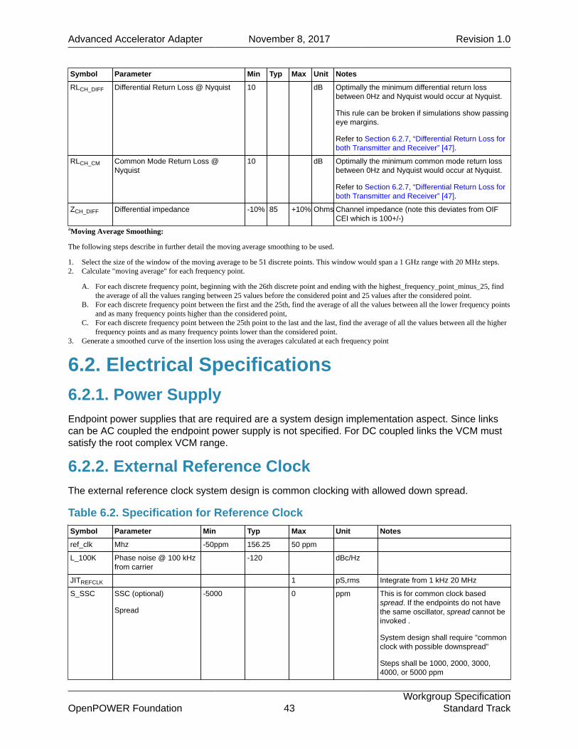
RLCH_DIFF Differential Return Loss @ Nyquist 10 dB Optimally the minimum differential return lossbetween 0Hz and Nyquist would occur at Nyquist.
This rule can be broken if simulations show passingeye margins.
Refer to Section 6.2.7, “Differential Return Loss forboth Transmitter and Receiver” [47].
RLCH_CM Common Mode Return Loss @Nyquist
10 dB Optimally the minimum common mode return lossbetween 0Hz and Nyquist would occur at Nyquist.
Refer to Section 6.2.7, “Differential Return Loss forboth Transmitter and Receiver” [47].
ZCH_DIFF Differential impedance -10% 85 +10% Ohms Channel impedance (note this deviates from OIFCEI which is 100+/-)
aMoving Average Smoothing:
The following steps describe in further detail the moving average smoothing to be used.
1. Select the size of the window of the moving average to be 51 discrete points. This window would span a 1 GHz range with 20 MHz steps.2. Calculate "moving average" for each frequency point.
A. For each discrete frequency point, beginning with the 26th discrete point and ending with the highest_frequency_point_minus_25, findthe average of all the values ranging between 25 values before the considered point and 25 values after the considered point.
B. For each discrete frequency point between the first and the 25th, find the average of all the values between all the lower frequency pointsand as many frequency points higher than the considered point,
C. For each discrete frequency point between the 25th point to the last and the last, find the average of all the values between all the higherfrequency points and as many frequency points lower than the considered point.
3. Generate a smoothed curve of the insertion loss using the averages calculated at each frequency point
6.2. Electrical Specifications6.2.1. Power SupplyEndpoint power supplies that are required are a system design implementation aspect. Since linkscan be AC coupled the endpoint power supply is not specified. For DC coupled links the VCM mustsatisfy the root complex VCM range.
6.2.2. External Reference ClockThe external reference clock system design is common clocking with allowed down spread.
Table 6.2. Specification for Reference ClockSymbol Parameter Min Typ Max Unit Notes
ref_clk Mhz -50ppm 156.25 50 ppm
L_100K Phase noise @ 100 kHzfrom carrier
-120 dBc/Hz
JITREFCLK 1 pS,rms Integrate from 1 kHz 20 MHz
S_SSC SSC (optional)
Spread
-5000 0 ppm This is for common clock basedspread. If the endpoints do not havethe same oscillator, spread cannot beinvoked .
System design shall require "commonclock with possible downspread"
Steps shall be 1000, 2000, 3000,4000, or 5000 ppm

Advanced Accelerator Adapter November 8, 2017 Revision 1.0
OpenPOWER Foundation 44Workgroup Specification
Standard Track
Symbol Parameter Min Typ Max Unit Notes
FM_SSC Modulation freq 30 33 kHz
TREFCLK Routing between Rx/Tx 10 nS Insertion delay between chips
AMPREFCLK Differential voltage swing 0.575 0.85 Vppd POWER9 uses SILabs HSCL driver
VCMREFCLK Common mode .35 0.4 V
FAC_REFCLK AC coupling (Required) 10 kHz AC coupling at the HPF corner
If 0-1V is incompatible with theendpoint VCM then AC coupling mustbe added.
TRREFCLK Rise/Fall time 0.2 1 nS 20-80% and the voltage swing is 0-1Vwith SST driver
ZDIFF_REFCLK Differential impedance -10% 85 +10% Ohms
6.2.3. CDR PLLTable 6.3. Specification for CDR PLL
Parameter Min Typ Max Unit Description
LC2 VCO Frequency -10% 25.78125G +10% GHz Tuning range of VCO_2
POWER9 PLL Lock time 5 mS Calibration, acquisition and lock fromPWR_GOOD [22].
Loop BW 2 3 8 MHz Programmable BW. Loop BW shall trackSSC, if present
Peaking 0 2 dB Programmable Damping
RJ Jitter (absolute) 0.2 ps RMS jitter spec of PLL output clockmeasured from baud/1667 to baud/2
6.2.4. IO LaneTable 6.4. Electrical Spec: Tx and Rx Termination
Symbol Parameter Min Typ Max Unit Notes
ZDIFF_IO Differential impedance 85 Ohms During normal mode and IDLEmode.
ZSE_IO Single ended impedance 43 Ohms The two single endedresistances shall match within10%.
dVGND,TxRx Ground difference 50 mVpp Ground differences between Txand far-end Rx
IL(TX) POWER9 TX has ACboost
-0.5 dB POWER9 TX at Pad hasBOOST
ILIO BW or loss due to poles -1 -1.5 dB A total budget of 3 dB for (Tx +Rx).
RLDIFF_IO Differential return loss dB More details in template inSection 6.2.7, “DifferentialReturn Loss for both Transmit-ter and Receiver” [47].
RLCM_IO Common-mode returnloss
dB More details in template inSection 6.2.8, “Common todifferential mode and differen-tial to common mode conver-sion” [48].

Advanced Accelerator Adapter November 8, 2017 Revision 1.0
OpenPOWER Foundation 45Workgroup Specification
Standard Track
6.2.5. Endpoint Transmitter
6.2.5.1. Electrical Output Specification
This section describes the Endpoint Transmitter Electrical Output Specification. This specificationis essentially the same as OIF CEI 28G SR and is enumerated in Table 6.5, “Endpoint TransmitterElectrical Output Specification. ” [45]. Key exceptions are identified via italics and highlighted inred.
Table 6.5. Endpoint Transmitter Electrical Output Specification.
Characteristic Symbol Condition MIN. TYP. MAX. UNIT
Baud Rate T_Baud 25.78125 Gsym/s
Output Differential Voltage T_Vdiff Note 4 800 1200 mVppd
Differential Resistance T_Rd Channels are designed 85ohms typical (Note 3)
85 Ohm
Differential Termination ResistanceMismatch
T_Rdm 10% %
Output Rise and Fall Time (20% to80%)
T_tr, T_tf Emphasis off (Note 2) 8 ps
Common Mode Noise T_Ncm Note 4 12 mVrms
Differential Output Return Loss T_SDD22 See Section 6.2.7, “Differ-ential Return Loss for bothTransmitter and Receiv-er” [47] curves copiedfrom OIF 28G spec
dB
Below 10 Ghz -6Common Mode Output Return Loss T_SCC22
10GHz to Baud rate -4
dB
Output Common Mode Voltage T_Vcm Load type 0 -100 -1700 mV
NOTES:
1. Load type 0 is AC coupled. The AC coupling caps exist near the endpoint devices2. The transmitter under test is preset such that C0 is its maximum value (C0_max) and all other coefficients are zero. The 20%
and 80% values are of the steady state one and zero. The max value is limited by meeting the transmit launch s12 of 0dB3. Nominal 85 ohm channels are designed from C4-C4. Endpoint package traces of endpoint module should also be defined to
be 85 ohms. If the endpoint is 100ohms in the silicon and the package is 100 ohms then regression is required to insure theILD is acceptable.
4. Procedure defined below from OIF CEI 28G specification,
6.2.5.2. Endpoint TX Jitter Models
The jitter terms below are specified at the PAD or C4 the chip carrier organic package is consideredpart of the channel.
Compliance to the TX model is defined by following the direction of the OIF CEI 28G VSR and SRstandards.
The TX jitter test methods follow the test methodologies of OIF CEI-28G-SR. Table 6.6, “Transmit-ter Output Jitter Specification for endpoint ( from CEI 28G SR )” [46] can be used as the jitterparameters for simulating the the channel. Alternately, the modelling may use the POWER9 TX infofound in Section A.3.2, “POWER9 TX Jitter Terms” [54] for the transmitter if the endpoint is onlyintended to connect to Power9.

Advanced Accelerator Adapter November 8, 2017 Revision 1.0
OpenPOWER Foundation 46Workgroup Specification
Standard Track
Table 6.6. Transmitter Output Jitter Specification for endpoint ( from CEI 28G SR )Characteristic Symbol Condition MIN. TYP. MAX. UNIT
Uncorrelated Unbounded GaussianJitter
T_UUGJ 0.15 UIPP
Uncorrelated Bounded HighProbability Jitter
T_UBHPJ Note 2 0.15 UIPP
Duty Cycle Distortion (componentof UBHPJ)
T_DCD Note 3 0.035 UIPP
Total Jitter T_TJ Note 1 0.28 UIPP
NOTES:
1. T_TJ includes all of the jitter components measured without any transmit equalization.2. Measured with all possible values of transmitter equalization, excluding DDJ as defined in the Section below.3. included in T_UBHPJ
6.2.6. Endpoint Receiver6.2.6.1. Electrical Input SpecificationThis section describes the Endpoint Receiver Electrical Output Specification. This specificationis essentially the same as OIF CEI 28G SR and is enumerated in Table 6.7, “ Endpoint ReceiverElectrical Input Specification. ” [46]. Key exceptions are identified via italics and highlighted in red.
Table 6.7. Endpoint Receiver Electrical Input Specification.Characteristic Symbol Condition MIN. TYP. MAX. UNIT
Baud Rate R_Baud 25.78125 Gsym/s
Input Differential Voltage R_Vdiff Note 1 1200 mVppd
Differential Input Impedance R_Rdin Channels are designed 85ohms typical
85 Ohm
Differential Termination ResistanceMismatch
R_Rdm 10% %
Differential Output Return Loss R_SDD11 See Section 6.2.7, “Differ-ential Return Loss for bothTransmitter and Receiv-er” [47] curves copiedfrom OIF 28G SR spec(14.3.2.5)
dB
Below 10 Ghz -6Common Mode Output Return Loss R_SCC11
10GHz to Baud rate -4
dB
Input Common Mode Voltage R_Vcm Load type 0 -100 1800 mV
NOTES:
1. The receiver shall have a differential input range sufficient to accept a signal produced at point R by the combined transmitterand channel. The channel response shall include the worst case effects if the return losses at the transmitter and receiver.
2. Load type 0 with min. T_Vdiff, AC-Coupling or floating load. For floating load, input resistance shall be >1 kOhm.
6.2.6.2. Endpoint Receiver Input Jitter Specification.
Table 6.8. Endpoint Receiver Input Jitter Specification.Characteristic Symbol Condition MIN. TYP. MAX. UNIT
Sinusoidal Jitter, Maximum R_SJ-max CEI OIF 28G SR section2.5.4 (Note 1)
5 UIpp

Advanced Accelerator Adapter November 8, 2017 Revision 1.0
OpenPOWER Foundation 47Workgroup Specification
Standard Track
Characteristic Symbol Condition MIN. TYP. MAX. UNIT
Sinusoidal Jitter, High Frequency R_SJ-hf CEI OIF 28G SR section2.5.4 (Note 1)
0.05 UIpp
NOTES:
1. The receiver shall tolerate the sum of these jitter contributions. Total transmitter jitter from table in TX section ; Sinusoidal jitteras defined in receiver section; The effects if the channel compliant to the Channel Characteristics.
6.2.7. Differential Return Loss for both Transmitter andReceiverThe required Differential return loss curve is the OIF CEI 28G SR specs. The table is recopiedbelow.
The sdd11 and sdd22 are the OIF-CEI-28G compliance curve

Advanced Accelerator Adapter November 8, 2017 Revision 1.0
OpenPOWER Foundation 48Workgroup Specification
Standard Track
Figure 6.1. SDD11 and SDD22 differential return loss at C4(PADS) template for RXand TX.
6.2.8. Common to differential mode and differential tocommon mode conversionThe common to differential mode and differential to common mode conversion specifications areintended to limit the amount of unwanted signal energy that is allowed to be generated due toconversion of common mode voltage to differential mode voltage or vice versa. When measured atthe respective input test point, common to differential mode or differential to common mode conver-sion shall not exceed the limits illustrated in Figure 6.2, “SDC11 and SCD11 for module input (TP1)and host input (TP4a) (for fb = 28 GHz)” [49].
Figure 6.2, “SDC11 and SCD11 for module input (TP1) and host input (TP4a) (for fb = 28GHz)” [49] is the OIF-CEI-28G compliance curve given by Section 6.2.8, “Equation Y” [49].

Advanced Accelerator Adapter November 8, 2017 Revision 1.0
OpenPOWER Foundation 49Workgroup Specification
Standard Track
Figure 6.2. SDC11 and SCD11 for module input (TP1) and host input (TP4a) (for fb= 28 GHz)
Equation YSDC11, SCD11 < -22 + 14 * ( f / fb ) dB for 0.05 < f < fb/2
SDC11, SCD11 < -18 + 6 * ( f / fb ) dB for fb/2 < f < fb
6.2.9. Common Mode NoiseThe Common Mode Noise is measured in compliance with CEI 28G SR

Advanced Accelerator Adapter November 8, 2017 Revision 1.0
OpenPOWER Foundation 50Workgroup Specification
Standard Track
7. OIF CEI 28G Compliance
Table of Contents7.1. Approach ............................................................................................................................... 507.2. Data Dependent Jitter (DDJ) measurement from CEI 28G SR ............................................... 507.3. Endpoint compliance TX jitter models for channel simulation ................................................. 517.4. Receiver Compliance ............................................................................................................ 52
7.1. ApproachThe range of channel designs encountered when interfacing to the Power9_25Gigabit PHY areexpected to deviate somewhat from the Industry Standard Specs of OIF CEI 28G VSR and OIFCEI 28G SR. These channels will be greater in loss then the Industry Standard Spec of OIF CEI28G VSR and less in loss than OIF CEI 28G SR. All compliance testing done for OIF CEI 28G SRis directly applicable and does not need to be repeated. If the endpoint PHY is SR compliant theendpoint PHY most likely has more RX equalization then would be optimal but should be adequate.The rational is as follows:
• The channel loss C4 to C4 is specified at 21 dB.• The OIF CEI 28G VSR specifies the loss at 10dB module-module.• If a token 3 dB per endpoint (module to c4) is assumed then the equivalent VSR C4 to C4 result
would be 16dB. A loss of 16dB is typically CTLE equalizable.• Assuming SR wire length adds another 5 dB if you use the same token 3dB per end giving the
resultant to be 21dB.
Note
To ensure operating margin the endpoint IP provider is strongly suggested to simulatethe full channel model in their simulator of choice.
Reference channel models are available at: https://members.openpowerfoundation.org/document/dl/453.
S-Parms are available at: https://members.openpowerfoundation.org/document/dl/455.
IBM Engineering support is available. See Section A.5, “Contacting IBM forAssistance” [57].
7.2. Data Dependent Jitter (DDJ) measurementfrom CEI 28G SRA high-resolution oscilloscope, time interval analyzer, or other instrument with equivalent capabili-ty may be used to measure DDJ. Establish a crossing level equal to the average value of the entirewaveform being measured.

Advanced Accelerator Adapter November 8, 2017 Revision 1.0
OpenPOWER Foundation 51Workgroup Specification
Standard Track
Synchronize the instrument to the pattern repetition frequency and average the waveforms or thecrossing times sufficiently to remove the effects of random jitter and noise in the system. The meantime of each crossing is then compared to the expected time of the crossing, and a set of timingvariations is determined. DDJ is the range (max-min) of the timing variations. Keep track of thesigns (early/late) of the variations. Note, it may be convenient to align the expected time of one ofthe crossings with the measured mean crossing. All edges of the repeating pattern that have beenaveraged need to be included in the measurement.
Figure 7.1, “DDJ Measurement Method” [51] below illustrates the method. The vertical axis is inarbitrary units, and the horizontal axis is plotted in UI. The waveform is AC coupled to an averagevalue of 0, therefore 0 is the appropriate crossing level. The rectangular waveform shows the expect-ed crossing times, and the other is the waveform with jitter that is being measured. Only 16 UI areshown in this example. The waveforms have been arbitrarily aligned with (delta t2 = 0) at 5 UI.
Figure 7.1. DDJ Measurement Method
7.3. Endpoint compliance TX jitter models forchannel simulationA TX model for compliance will be formulated as follows:
CEI TX Jitter InteractionsThe jitter terms below are specified at the PAD or C4 the chip carrier organic package is consideredpart of the channel.
Using the Dual Dirac jitter model[1], total jitter (TJ) is given by Eq. (1)

Advanced Accelerator Adapter November 8, 2017 Revision 1.0
OpenPOWER Foundation 52Workgroup Specification
Standard Track
where Q (BER) is Q-factor, both RJ and BUJ are assumed as Gaussians down to 1e-15 probability;σRJ and σBUJ are rms values for RJ and BUJ respectively. We could rewrite Eq (1) in terms of pk-pkvalues of RJ and BUJ as the following Eq (2)
For CEI[2], we have TDCD =0.035 UI, TRJ = 0.15 UI, TBUJ= 0.15 UI, TTJ =0.28 UI, and with Eq. (2), weget TDDJ = 0.0329 UI.
By specifying the upper bounds of TDCD , TRJ , TBUJ, TTJ , it implicitly specifies the upper limit forDDJ, as such all the jitter components are bounded and limited.
7.4. Receiver ComplianceThis section is taken from section 2.5.4 in the OIF_CEI_28G_SR specification. All references are tothe OIF_CEI_28G-SR specification and the reader is refered to that specification for further details.
The following steps shall be made to identify whether a receiver is considered compliant.
1. The DUT shall be measured to have a BER1 better than specified for a stressed signal (seeAppendix 2.E.4.2 for a suggested method) with a confidence level of three sigma (see Appendix2.F.2. for a suggested method) given
• for non-transparent applications, the defined sinusoidal jitter mask for relative and totalwander as per Annex 2.A.1 and Annex 2.A.2, with a high frequency total/relative wander anda maximum total/relative wander as defined in the Implementation Agreement
• for transparent application, the defined appropriate sinusoidal jitter mask for the specificoptical standard
• the high frequency jitter should be calibrated by either:
– applying the maximum specified amount of receiver High Probability Jitter and Gaussianjitter2 including CBHPJ
or
– applying the maximum specified amount of receiver High Probability Jitter and Gaussianjitter3 excluding CBHPJ
– cascading with a compliance channel or filter as identified by 2.5.2.
– applying an additive crosstalk signal of amplitude such that the resulting statisticaleye, given the channel, jitter and crosstalk, is as close as feasible in amplitude whencompared to the defined minimum amplitude for channel compliance

Advanced Accelerator Adapter November 8, 2017 Revision 1.0
OpenPOWER Foundation 53Workgroup Specification
Standard Track
Appendix A. IBM® POWER9™ SpecificInformationA.1. Global ParametersTable A.1. Global ParametersParameter Specification
Data rate 25.78125 Gbps (other speeds possible)
POWER9 I/O Power Supply Min Typ Max
VIO 0.95V 1.0V 1.125V
VDN( logic supply ) = 0.7V nominal and is adaptive
POWER9 Temperature (junction) TJ -10C to 85C
Termination 85 Ohms differential at Rx , POWER9 TX is SST with 42.5 Ohms from VIO to PAD and42.5 Ohms from PAD to GND ( 85 Ohms is a deviation from the OIF CEI 28G SR specifica-tion which defines the nominal impedance as 100 Ohms )
ESD 1000V HBM, 200V CDM (This is outside of the OIF CEI SR spec)
POWER9 PHY Latency Core to TX driver output: 17 UI; RX sampler to Core interface:17 UI
A.2. IBM POWER9 Nominal Estimated PowerDissipationThe power budget breakdown at 25 Gbps for some of the major blocks within a IOLANE are shownbelow. Numbers reported below for some of the shared blocks outside of the IOLane, such as thePLL, are amortized, per lane values. The overall link efficiency is targeted around 5-6 pJ/b at 25Gbps (1Tx + 1Rx + PLL). The PLL amortized over 24 lanes in the POWER9 Processor.
A.3. POWER9 TransmitterA.3.1. Electrical Spec: POWER9 TxTable A.2. Electrical Spec: POWER9TxSymbol Parameter Min Typ Max Unit Notes
FBAUD Baud rate 25.78125 Gbps
VTX-DIFF-PP Differential p-p Tx voltageswing
900 1000 1100 mV TX launch into a DC matched
85 ohm system
VTX_CM_DC Tx Output CM 0.475 0.5 0.562 CM during normal operation andduring RxCAL mode. For DCcoupled systems
VTX-CM-AC AC CM ripple 25 mVp Measured up to Fbaud.
VDIFF_RxCAL -10 0 10 mV Differential voltage duringRxCAL.
RTXRxCAL Impedance during RxCAL 95 170 Ohms
TRTX Rise/fall time at Tx TBD psec 20% - 80 %, In TX Sparms

Advanced Accelerator Adapter November 8, 2017 Revision 1.0
OpenPOWER Foundation 54Workgroup Specification
Standard Track
Symbol Parameter Min Typ Max Unit Notes
TX_S21 Insertion loss at Nyquist -0.5 dB POWER9 TX has boost, fromsimulation.
TX FIR Tx de-emphasis:
C-1,C 0, C+1
|C0| + |C+1| + |C-1 |= 1
Ci resolution to be better than1/36.
(POWER9 does not implementC+1)
A.3.2. POWER9 TX Jitter TermsThe jitter terms are specified at the PAD or C4 the chip carrier organic package is considered part ofthe channel.
NoteJitter terms for inclusion in channel sims for POWER9 can be provided.
POWER9 TX silicon S-parameter models are available upon request.
See Section A.5, “Contacting IBM for Assistance” [57].
A.3.3. POWER9 TX SST termination picture excludingTcoils and ESD affectsFigure A.1. POWER9 TX SST termination picture excluding Tcoils and ESD affectsadded to the RX above

Advanced Accelerator Adapter November 8, 2017 Revision 1.0
OpenPOWER Foundation 55Workgroup Specification
Standard Track
A.4. POWER9 ReceiverA.4.1. Electrical Spec: RxBelow is the characteristics of the POWER9 Rx design this does not preclude other equalizationmethod of choice.
The design must be able to equalize the channel without a back channel to TX_EQ like PCI-G3/G4and the POWER9 TX will only have a pre-cursor.
Table A.3. Rx Electrical SpecSymbol Parameter Min Typ Max Unit Notes
VRX-DIFF-PP Diff Rx p-p voltage 1100 mVppd
BER Target BER 10-15 Extrapolated where needed.
VNRX Input referred electrical noise 4.0 mVrms Integrated from 1 MHz
JTOL(f) Jitter tolerance.
F_jitter > Fbaud/200
F_jitter < Fbaud/25000
0.1
10
UIpp
UIpp
Measured at 10-15 BER
More details in template.
VRX-SEN Receiver input sensitivity 50 mVppd Measured from breakout board.
CTLEBOOST Rx CTLE boost ratio 12 dB See curves
H0 DFE Target 50 100 150 mVpp
Hi
i = 1
DFE tap weight
H1
0 0.7 *h0 Resolution of Hi to be betterthan h0/48. (POWER9 RXimplements only H1)
LTEQZERO 200 MHz Long tail EQ
LTEQPOLE 333 MHz Long tail EQ
LTEPEAK 3.5 dB Gain range of LTE (LTE will befixed) DC is at -3.5dB
VRX-CM Input CM voltage (DC) 0.45 0.5 0.562 V Floating termination.
CDR BW CDR BW of first order loop 10 MHz Some programmability
CDRPeaking
Peaking/overshoot 0.5 dB
TRX-LATENCY
Rx data path latency 24 UI Latency defined from arrival ofbit at Rx input to rising edge of.
P-N skew In pair skew 0.25 UI The POWER9 RX can tolerate25% P-N before additive jitteroccurs
A.4.2. POWER9 RX jitter termsThe jitter terms are specified at the PAD or C4 the chip carrier organic package is considered part ofthe channel.
NoteJitter terms for inclusion in channel sims for POWER9 can be provided.
RX silicon S-parameter models are available upon request inclusive of CTLE variances( many S paramters)

Advanced Accelerator Adapter November 8, 2017 Revision 1.0
OpenPOWER Foundation 56Workgroup Specification
Standard Track
See Section A.5, “Contacting IBM for Assistance” [57].
A.4.3. POWER9 Rx termination picture excluding Tcoilsand ESD affects.For AC coupling we have a Vcc/2 bias method and the OpenCAOI protocol has 64/66 coding forclock compensation and scrambling to limit baseline wander.For AC coupling we have a Vcc/2 biasmethod and the OpenCAPI protocol has 64/66 coding for clock compensation and scrambling to limitbaseline wander.
Figure A.2. POWER9 Rx termination picture excluding Tcoils and ESD affects.

Advanced Accelerator Adapter November 8, 2017 Revision 1.0
OpenPOWER Foundation 57Workgroup Specification
Standard Track
A.4.4. POWER9 RX CTLE+LFEQ suite of curve in Sparameter formFigure A.3. POWER9 RX CTLE+LFEQ suite of curve in S parameter form
A.5. Contacting IBM for AssistanceSupport for developers within the OpenPOWER ecosystem may be obtained from IBM. Informationis available on the IBM Portal for OpenPOWER https://www-335.ibm.com/systems/power/openpow-er/.
To email IBM Support for OpenPOWER: <[email protected]>

Advanced Accelerator Adapter November 8, 2017 Revision 1.0
OpenPOWER Foundation 58Workgroup Specification
Standard Track
Appendix B. ReferencesB.1. OIF CEI 28Gbps SR SpecificationThe OIF CEI 28Gbps SR Specification was referenced in this specification document and in somecases copied. To include the OIF content in this document, the following notices are required.
2014© Optical Internetworking Forum
This document and translations of it may be copied and furnished to others, and derivative worksthat comment on or otherwise explain it or assist in its implementation may be prepared, copied,published and distributed, in whole or in part, without restriction other than the following, (1) theabove copyright notice and this paragraph must be included on all such copies and derivative works,and (2) this document itself may not be modified in any way, such as by removing the copyrightnotice or references to the OIF, except as needed for the purpose of developing OIF ImplementationAgreements.

Advanced Accelerator Adapter November 8, 2017 Revision 1.0
OpenPOWER Foundation 59Workgroup Specification
Standard Track
Appendix C. OpenPOWER FoundationoverviewThe OpenPOWER Foundation was founded in 2013 as an open technical membership organiza-tion that will enable data centers to rethink their approach to technology. Member companies areenabled to customize POWER CPU processors and system platforms for optimization and innova-tion for their business needs. These innovations include custom systems for large or warehousescale data centers, workload acceleration through GPU, FPGA or advanced I/O, platform optimiza-tion for SW appliances, or advanced hardware technology exploitation. OpenPOWER members areactively pursing all of these innovations and more and welcome all parties to join in moving the stateof the art of OpenPOWER systems design forward.
To learn more about the OpenPOWER Foundation, visit the organization website atopenpowerfoundation.org.
C.1. Foundation documentationKey foundation documents include:
• Bylaws of OpenPOWER Foundation
• OpenPOWER Foundation Intellectual Property Rights (IPR) Policy
• OpenPOWER Foundation Membership Agreement
• OpenPOWER Anti-Trust Guidelines
More information about the foundation governance can be found at openpowerfoundation.org/about-us/governance.
C.2. Technical resourcesDevelopment resouces fall into the following general categories:
• Foundation work groups
• Remote development environments (VMs)
• Development systems
• Technical specifications
• Software
• Developer tools
The complete list of technical resources are maintained on the foundation Technical Resources webpage.

Advanced Accelerator Adapter November 8, 2017 Revision 1.0
OpenPOWER Foundation 60Workgroup Specification
Standard Track
C.3. Contact the foundationTo learn more about the OpenPOWER Foundation, please use the following contact points:
• General information -- <[email protected]>
• Membership -- <[email protected]>
• Technical Work Groups and projects -- <[email protected]>
• Events and other activities -- <[email protected]>
• Press/Analysts -- <[email protected]>
More contact information can be found at openpowerfoundation.org/get-involved/contact-us.