coMbinEd ElEcTro-MEchanical MEMS TESTing - … · coMbinEd ElEcTro-MEchanical MEMS TESTing ......
13
FEMTO TOOLS COMBINED ELECTRO-MECHANICAL MEMS TESTING FT-MPS02 MEMS PROBESTATION Product Brochure
Transcript of coMbinEd ElEcTro-MEchanical MEMS TESTing - … · coMbinEd ElEcTro-MEchanical MEMS TESTing ......

FEMTO TOOLS
coMbinEd ElEcTro-MEchanical
MEMS TESTing
FT-MPS02MEMS ProbESTaTion
Product Brochure

Overview 3
ApplicAtiOn exAmple: mechAnicAl testing 11
ApplicAtiOn exAmple: thermAl ActuAtOr testing 15
micrOmechAnicAl testing mOdule 5
ApplicAtiOn exAmple: piezOresistive sensOr testing 12
mAnuAl prObestAtiOn And electricAl sOurces And meters 9
ApplicAtiOn exAmple: piezOelectric ActuAtOr testing 13
ApplicAtiOn exAmple: electrOstAtic ActuAtOr testing 16
AccessOries 17
technicAl specificAtiOns 19
duAl micrOscOpe with tOuchscreen interfAce 7
ft-mps02
electrO-mechAnicAl testingmems prObestAtiOn
1 2ContentFT-MPS02 MEMS Probestation

4
1
2
3
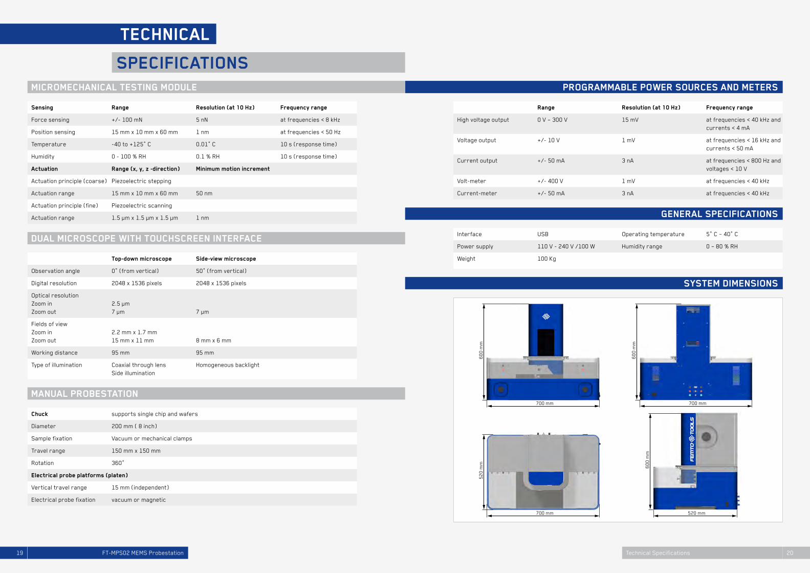
micromechanical testing module: The micromechanical testing module is a high-precision, force-probe-based sys-tem that allows for the quantitative measurement of mechanical and geometrical properties of microstructures.
dual microscope with touchscreen interface: The combination of a calibrated top-down microscope with motorized zoom and a 50° side-view microscope allows for the visual inspection and observation during testing.
manual probestation: The base of the FT-MPS02 MEMS Probestation is a high-precision, easy-to-use manual probestation for wafers and substrates up to 200 mm (8 inch) in diameter.
programmable voltage/current sources and multimeter: The FT-MPS02 MEMS Probestation features a variety of programmable power sources and meters. Therefore, the automated and user-friendly electrical testing of MEMS devices and circuits is possible without the need of any auxiliary equipment.
mems prObestAtiOn
ft-mps02
Micro-Electro-Mechanical Systems (MEMS) combine elec-trical as well as mechanical aspects on a single chip. For this reason, not only electrical, but also mechanical pro-perties of these sensors and actuators provide valuable insights into their functionality and reliability.
The FT-MPS02 MEMS Probestation is a wafer-level MEMS testing instrument that allows for the fast, user-friendly and simultaneous testing of mechanical, electrical and geometrical properties on MEMS chips.
The FT-MPS02 MEMS Probestation combines a micro-mechanical testing module with a manual probestation, a motorized dual measurement microscope, programmable voltage/current sources and a multimeter. Besides the capabilities of each of the four individual modules, the FT-MPS02 MEMS Probestation also features a wide range of additional capabilities that result from the combination and synchronization of the modules in one measurement sys-tem, such as the combined electro-mechanical testing.
The FT-MPS02 MEMS Probestation greatly improves the efficiency of MEMS development. It allows for the quantita-tive characterization of the micromanufacturing process steps and provides feedback to improve the mathematical models used to design MEMS. Furthermore, it enables the mechanical testing of MEMS prototypes directly on the wa-fer without the need of wafer dicing and wire-bonding.
Actuator testing and calibration Etch-depth
wafer level mems testing fabrication process
and calibration feedback
Electrical testing Release and stiction detection
Fabrication yield
Layer thickness (step-height)
Mechanical testing (in-plane / out-of-plane) Over- and under-etch
Sensor testing and calibration Process uniformity
Key cApAbilities
electrO-mechAnicAl mems testing
14
2
3
Overview
The combined, wafer-level electro- mechanical testing can provide valu-able insights into the design, fab-rication and functionality of MEMS. Furthermore, through periodic test-ing along the microfabrication process sequence, each step can be monitored and verified. These in-process test-ing steps offer a great potential to increase the overall fabrication yield.
The unique FemtoTools Microforce Sensing Probes for in-plane and out-of-plane mechanical MEMS testing.
3 4OverviewFT-MPS02 MEMS Probestation
41
25
3
7
8
9
106
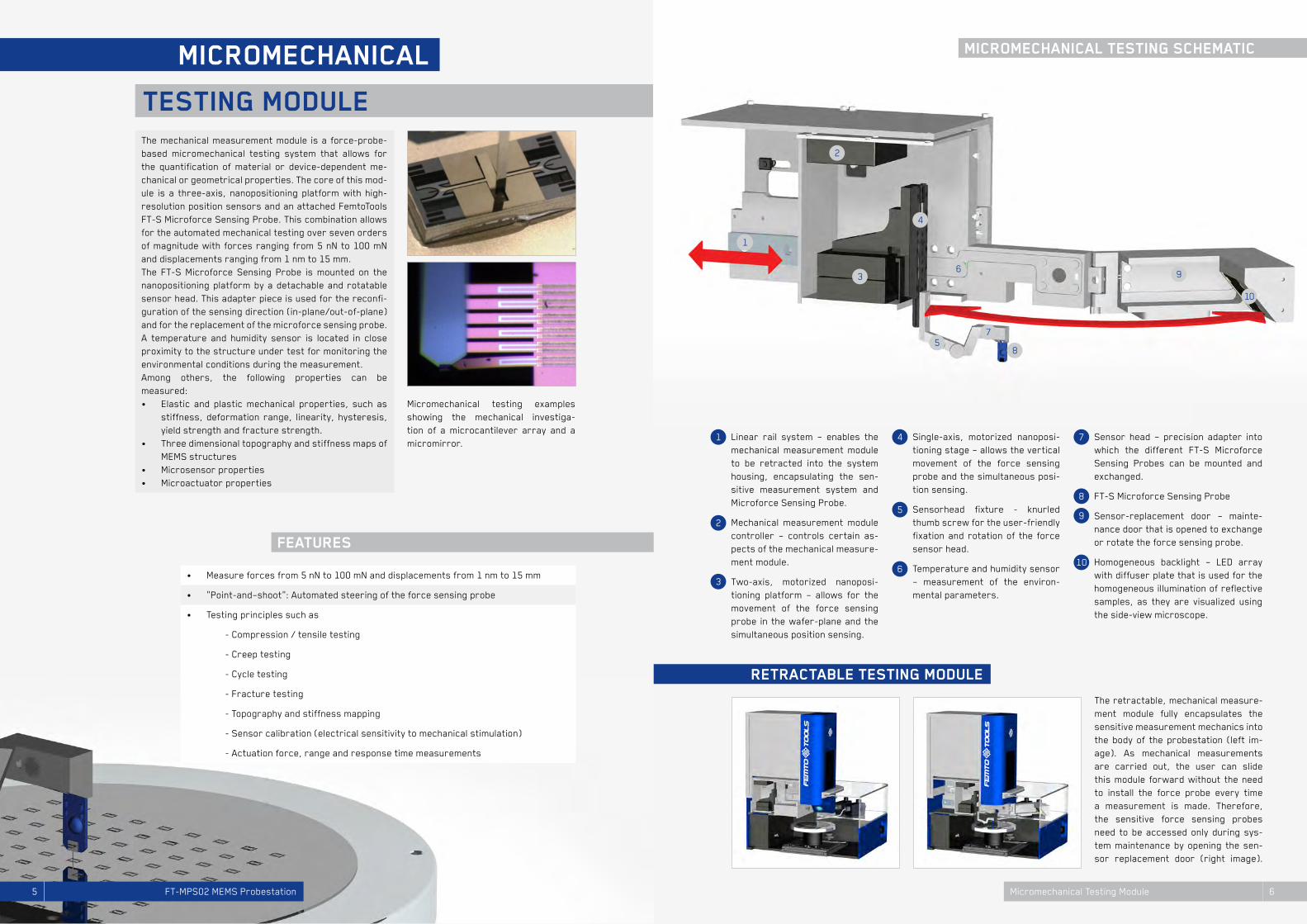
Linear rail system – enables the mechanical measurement module to be retracted into the system housing, encapsulating the sen-sitive measurement system and Microforce Sensing Probe.
Mechanical measurement module controller – controls certain as-pects of the mechanical measure-ment module.
Two-axis, motorized nanoposi-tioning platform – allows for the movement of the force sensing probe in the wafer-plane and the simultaneous position sensing.
Single-axis, motorized nanoposi-tioning stage – allows the vertical movement of the force sensing probe and the simultaneous posi-tion sensing.
Sensorhead fixture - knurled thumb screw for the user-friendly fixation and rotation of the force sensor head.
Temperature and humidity sensor – measurement of the environ-mental parameters.
Sensor head – precision adapter into which the different FT-S Microforce Sensing Probes can be mounted and exchanged.
FT-S Microforce Sensing Probe
Sensor-replacement door – mainte-nance door that is opened to exchange or rotate the force sensing probe.
Homogeneous backlight – LED array with diffuser plate that is used for the homogeneous illumination of reflective samples, as they are visualized using the side-view microscope.
testing mOdule
micrOmechAnicAl
The mechanical measurement module is a force-probe-based micromechanical testing system that allows for the quantification of material or device-dependent me-chanical or geometrical properties. The core of this mod-ule is a three-axis, nanopositioning platform with high-resolution position sensors and an attached FemtoTools FT-S Microforce Sensing Probe. This combination allows for the automated mechanical testing over seven orders of magnitude with forces ranging from 5 nN to 100 mN and displacements ranging from 1 nm to 15 mm.The FT-S Microforce Sensing Probe is mounted on the nanopositioning platform by a detachable and rotatable sensor head. This adapter piece is used for the reconfi-guration of the sensing direction (in-plane/out-of-plane) and for the replacement of the microforce sensing probe. A temperature and humidity sensor is located in close proximity to the structure under test for monitoring the environmental conditions during the measurement.Among others, the following properties can be measured:• Elastic and plastic mechanical properties, such as
stiffness, deformation range, linearity, hysteresis, yield strength and fracture strength.
• Three dimensional topography and stiffness maps of MEMS structures
• Microsensor properties• Microactuator properties
feAtures
retrActAble testing mOdule
1
4
2
7
10
58
3 96
micrOmechAnicAl testing schemAtic
The retractable, mechanical measure-ment module fully encapsulates the sensitive measurement mechanics into the body of the probestation (left im-age). As mechanical measurements are carried out, the user can slide this module forward without the need to install the force probe every time a measurement is made. Therefore, the sensitive force sensing probes need to be accessed only during sys-tem maintenance by opening the sen-sor replacement door (right image).
• Measure forces from 5 nN to 100 mN and displacements from 1 nm to 15 mm
• “Point-and–shoot”: Automated steering of the force sensing probe
• Testing principles such as
- Compression / tensile testing
- Creep testing
- Cycle testing
- Fracture testing
- Topography and stiffness mapping
- Sensor calibration (electrical sensitivity to mechanical stimulation)
- Actuation force, range and response time measurements
Micromechanical testing examples showing the mechanical investiga-tion of a microcantilever array and a micromirror.
5 6Micromechanical Testing ModuleFT-MPS02 MEMS Probestation

11
10
414
7
17
1
2
12
5
15
8
18
3
13
6
16
9
19
CMOS Camera, 3 megapixel (2048 x 1536 pixels)
Projection lens
Motorized 7:1 optical zoom
7” touch screen - display and control of the microscope, illumination and zoom
Prisms - couples the light into the optical path for the coaxial illumi-nation
Objective lens
Backlight - homogeneous illumi-nation for the side-view micro-scope
Microscope controller for the zoom, illumination and touch screen
LED light source, pure white (6’000 K)
Diffusor
Aspheric condenser lens
Mirror
Scheimpflug adjuster - for an in-focus visualization of the side-view microscope’s entire field of view
CMOS Camera, 3 megapixel (2048 x 1536 pixels)
Projection lens
Aperture
Mirror
Objective lens
Coarse/fine focus knob
with tOuchscreen interfAce
duAl micrOscOpe
The FT-MPS02 MEMS Probestation features two microscopes. The calibrated, top-view microscope with motorized zoom allows for the precise alignment of the electrical probes and visual sample inspection. The top-view mi-croscope features a coaxial- and side-light il-lumination. Depending on the reflectivity of the sample, either illumination is optimal. For the vertical, top-down micromechanical testing, the force sensing probe can obstruct the sam-ple. Therefore, a side-view microscope offers an alternative visualization. For especially this purpose, we developed the Scheimpflug-angu-lar-compensation adapter, which realizes an in-focus visualization of the entire field of view despite the large observation angle of 50° (to the vertical axis). For the side-view visualiza-tion, a homogenous backlight provides an ideal illumination for both highly reflective and non-reflective samples.The main purpose of the dual microscope with touchscreen is:• Visual inspection and dimensional meas-
urements• Mechanical and electrical probe alignment• Measurement observation and recording
feAtures
micrOscOpe imAges
1
11
104
14
717
2
125
15
8
18
3
13
6
16
9
19
micrOscOpe schemAtic
Comparison between the top-down microscope image (left) and the side-view microscope image (right) of an electrostatic micromirror. Even though the side-view microscope observes the sample under a large angle of 50°, the entire field of view is in focus with minimal perspective distortions.
• Motorized 7:1 zoom (field of view ranging from 15 mm x11 mm to 2.2 mm x 1.7 mm)
• 3 megapixel CMOS camera
50° side-view digital microscope with touch screen interface
• Field of view of 8 mm x 6 mm
• In-focus visualization of the entire field of view due to the Scheimpflug compensation
• Calibrated microscope for dimensional metrology and automated probe positioning
• Calibrated microscope for dimensional metrology and automated probe positioning
top-down digital microscope with touch screen interface
• Coaxial and side-light illumination
• Enables simultaneous mechanical testing and visualization
• Homogeneous backlight illumination
• 3 megapixel CMOS camera
Microscope images taken with the top-view microscope.
7 8Dual Microscope with Touchscreen InterfaceFT-MPS02 MEMS Probestation
1mm 1mm

61
27
5
4
3
11
12
13
14
8
9
10
Voltage/current inputs and out-puts
BNC feed-through
Vacuum for the electrical probes
Electrical probe
Vertically adjustable platform
Vertical platform adjustment knob
Top-view microscope
Mechanical measurement module
Wafer chuck
Wafer chuck rotation stage
Wafer chuck long-range positioning platform
Side-view microscope
System door
Vertically movable enclosure
electricAl sOurces And meters
mAnuAl prObestAtiOn And
The stable base of the FT-MPS02 is a high-precision, manual probestation for wafers and substrates up 200 mm (8 inch). It features a wafer chuck with a manual drive for two- axis, in-plane positioning as well as a rotation stage for the rotational alignment. On each side of the wafer chuck a vertically adjustable platform offers space for multiple electrical probes and their simultaneous vertical motion. The vertically movable enclosure and the front door provide a shield from air currents and prevent particle contamination while guaran-teeing ergonomic access to the sample and system controls. For electrical measurements in the low- frequency range, the FT-MPS02 MEMS Probestation features a variety of program-mable power sources and meters. Therefore, this probestation allows for the automated electrical testing of MEMS devices without the need of any auxiliary equipment. All sources and measurements are synchronized with each other and the micromechanical testing module. For specialized measurements the system offers 6 BNC feed-throughs that allow the use of auxiliary instruments. This enables e.g. the electrical testing at high-frequencies.
feAtures
electricAl mems prObing
1
11
10
4
14
72
12
5
5
8
3
13
6
6
9
prObestAtiOn schemAtic
The high-precision alignment of the electrical and mechanical probes on wafer level.
• 200 mm (8 inch) diameter wafer chuck (also supports single chips and small wafers)
• Precise chuck rotation stage for up to 360°
• Two vertical, independent adjustable steel platforms (platen)
• Force sensing probe and wafer chuck can be set to an electrical potential
• Vertical movable, weight-balanced enclosure
• Software controlled current-, low- and high-voltage power sources
- Measures V, I, and R
- Readout the electrical signal of microsensors
- Power microactuators (e.g. thermal, electrostatic, and piezoelectric)
• Wafer fixation by vacuum or mechanical clamps
manual probestation
• Precise chuck positioning along two-axis and a range of 150 mm x 150 mm
• Compatible with a large range of electrical probes (magnetic and vacuum fixation)
• Rigid microscope bridge (machined out of solid aluminum)
• Software controlled current, voltage and resistance measurement instrument
• 6 BNC feed-throughs for the integration of specialized, auxiliary instruments
programmable power sources and meters
Close-up image of the combined elec-trical and mechanical MEMS probing (upper image). The various connectors to the internal power source and me-ters (lower image).
9 10Manual Probestation and Electrical Sources and MetersFT-MPS02 MEMS Probestation

ApplicAtiOn exAmple
piezOresistive sensOr testingmechAnicAl testing
During the micro-manufacturing process development, a large num-ber of process parameters influ-ence the mechanical properties of the MEMS structures. In this applica-tion both the in-pane stiffness and out-of-plane stiffness of an array of MEMS flexures are tested using the FT-MPS02. By defining an upper and a lower limit for the target stiffness, a chip map is created to identify the working flexures (green) and flexures that are outside the desired specifi-cations (red). Flexures that have not been successfully released from the wafer (very high stiffness) or flex-ures with cracks (low stiffness) are identified. The yield rate can easily be detected by the ratio of green and red marks.
testing Of micrOfAbricAtiOn yield
0 2 4 60
200
400
600
800
1000
App
lied
forc
e (µ
N)
Sample deflection (µm)
out-of-planestiffness (N/m)
in-planestiffness (N/m)
200
240
280
Sti
ffne
ss (
N/m
)
functionality criteria
chip map
0 2 4 60
200
400
600
800
1000
App
lied
forc
e (µ
N)
Sample deflection (µm)
out-of-planestiffness (N/m)
in-planestiffness (N/m)
200
240
280
Sti
ffne
ss (
N/m
)
functionality criteria
chip map
An array of nanocantilevers for bio-logical screening applications has been fabricated featuring variable surface coatings at the nanocantilever tip. The FT-MPS02 system is used to measure both the elasticity of the nanocantile-ver and the adhesion force at the tip. The adhesion force corresponds to the negative “pulling” force during the un-loading of the nanocantilever.
A two-axis microscanner chip to be integrated in a barcode reader is me-chanically tested. The scanner con-sists of a square-shaped structure suspended by torsional beams and an inner, square-shaped mirror plate, which is suspended by another set of torsional springs. This configuration allows the inner mirror plate to deflect in two axes. A “stiffness-map” is cre-ated by performing vertical compres-sion tests to measure the device stiff-ness at a large number of locations on the mechanical structure.
nAnOcAntilever AdhesiOn fOrce testing
twO-Axis micrOscAnner testing
0
0.2
0.4
0.6
0 0.5 1.0
Posi
tion
(m
m)
Position (mm)1.5
0.8
1.0
1.2
1.4
0
100200300400500600700N/m
0 1 2 3 4−1
0
1
2
3
App
lied
forc
e (µ
N)
Sample deflection (µm)
adhesion force (µN)
piezOresistive cAntilever testing
To increase the efficiency of Dip-Pen nanolithography systems, MEMS chips featuring an array of 6 cantilevers have been fabricated for parallel writing. To correct for the tilt angle between the cantilever array and the sample substrate, the cantilevers have been equipped with piezoresistive sensors, which measure the contact force of each cantilever. The sensors have been fabricated by ion-implantation and a Wheatstone bridge has been integrat-ed to stabilize the signal. This applica-tion describes the electromechanical characterization of the piezoresistive cantilever arrays and the cantilever calibration on chip and wafer level. The first important device property tested is the stiffness (ratio of force to deflection) of each individual cantile-ver in the array. The FT-MPS02 MEMS Probestation is used to perform the compression tests. The force-deflec-tion curve for the two cantilevers is illustrated in the top graph. Next, the output signals of the canti-levers are tested with respect to the applied force. For this purpose, four electrical probes are brought into con-tact with the Wheatstone bridge while the FT-S Microforce Sensing Probe is applying loads onto the cantilever tip. By repeating the aforementioned measurements on all cantilever arrays within the wafer, the statistical distri-bution of the stiffness / sensitivity can be quantified. Additionally, by defining upper and lower limits for these prop-erties, defective devices can be de-tected before the laborious packaging step (chip dicing, chip gluing and wire-bonding). As shown in the lower graph, good devices are marked green while devices not fulfilling the specifications are marked red. Finally, the total yield rate of the manufacturing process can be evaluated.
Sample deflection (µm)
cantilever 1cantilever 2
App
lied
forc
e (µ
N)
Applied force (µN)
0 5 10 15 20 25
0
20
40
60
80
100
0 20 40 60 80 100Out
put
volt
age
chan
ge (
mV)
0
10
20
30
40
50
60
cantilever 1cantilever 2
3.5
3.0
4.5
5.5
5.0
4.0
Sti
ffne
ss (
N/m
)
440
430
non-functionalcantilever
functionalcantilever
560
580
570
450
Sen
siti
vity
(V/
N)
11 12Application ExampleFT-MPS02 MEMS Probestation

ApplicAtiOn exAmple
V
piezOelectric ultrAsOnic trAnsducer testing
piezOelectric ActuAtOr testing
1 stiffness 2 max. nonlinearity 3 contact point = topographic height 4 adhesion force 5 hysteresis
detail B
detail B
detail A
detail A
0.64 0.72 0.840
50
60
2
5
−10
0
0 10.2 0.4 0.6 0.8
10
20
30
40
50
60
70
80
90
100
App
lied
forc
e (µ
N)
Position (µm)
0.3 0.4−10
0
103
4
1
0 40 80 120 160 20020 60 100 140 180
0
0.5
1
1.5
2
2.5
Actuation voltage (V)
Vert
ical
pos
itio
n (µ
m)
Actu
atio
n fo
rce
(µN)
/
Actu
atio
n vo
ltage
(V)
0 0.1 0.2 0.3 0.4 0.5 0.6 0.7 0.8 0.9 1.00
50
100
150
200
Time (s)
200
240
280
Sti
ffne
ss (
N/m
)
functionality criteria
chip map
0 40 80 120 160 20020 60 100 140 180
0
0.5
1
1.5
2
2.5
Actuation voltage (V)
Vert
ical
pos
itio
n (µ
m)
Actu
atio
n fo
rce
(µN)
/
Actu
atio
n vo
ltage
(V)
0 0.1 0.2 0.3 0.4 0.5 0.6 0.7 0.8 0.9 1.00
50
100
150
200
Time (s)
200
240
280
Sti
ffne
ss (
N/m
)
functionality criteria
chip map
0
2
4
Z P
osit
ion
(µm
)
topography map atactuation voltage = 0 V 100 nm thick
Al pad
−2000
200
−2000
200
0
5
10
X Position (µm)Y Position (µm)
−2000
200
−2000
200X Position (µm)Y Position (µm)
0
2
4
Z P
osit
ion
(µm
)
−2000
200
−2000
200X Position (µm)Y Position (µm)
Com
plia
nce
(mm
/N) stiffness map at
actuation voltage = 0 V
topography map atactuation voltage = 150 VV
0
2
4
Z P
osit
ion
(µm
)
topography map atactuation voltage = 0 V 100 nm thick
Al pad
−2000
200
−2000
200
0
5
10
X Position (µm)Y Position (µm)
−2000
200
−2000
200X Position (µm)Y Position (µm)
0
2
4
Z P
osit
ion
(µm
)
−2000
200
−2000
200X Position (µm)Y Position (µm)
Com
plia
nce
(mm
/N) stiffness map at
actuation voltage = 0 V
topography map atactuation voltage = 150 VV
Two electrical probes in contact with the electrical pads at the border of the ultrasonic transducer array are mounted on the FT-MPS02 MEMS Probestation. This setup allows meas-uring the deflection and actuation force of the piezoelectric membranes with respect to the driving signal. Driving signals up to 200 V are generated by the FT-MPS02’s signal generator and applied to the individual membranes. This results in a membrane deflection of up to 2.5 μm at the center of the membrane. Topography maps at dif-ferent actuation voltages are created to quantify the shape of the deflected membranes with respect to the driving signals. The graphs on the left illus-trate the topography of the membrane at an actuation voltage of O V and 150 V, respectively. Prior to packaging (chip mounting, wire-bonding) a quality control of the ultrasonic transducer array is carried out in which all individual membranes on the transducer chip are tested. Pre-defined upper and lower bounda-ries for the center membrane stiffness as functionality criteria were used to detect defective specimens. Defective membranes are marked as red circles in the chip map. This quality control step ensures that the best transducer chips are selected on the wafer for further usage.
Micromachined ultrasonic transduc-ers have many applications such as range-finding, non-destructive test-ing and flow sensing. This application describes the quantitative, in-depth mechanical testing of an ultrasonic transducer array using the FT-MPS02 MEMS Probestation. Both, static me-chanical and electro-mechanical prop-erties are tested. The transducer ar-ray consists of 37 membranes with a diameter of 400 μm. The membranes include a buried aluminum nitride (AIN) layer for piezoelectric actuation and two metallic layers (aluminum and platinum) for electrical contacting of the individual membranes of the array. When applying an actuation voltage across the AIN layer the membranes deflect out-of-plane, which produces a pressure wave. The center point of the piezoelectric membrane is selected on the camera image for the mechanical testing. After the force sensing probe is automati-cally steered to the selected location a compression test was performed. The linearity and hysteresis of the result-ing force-deflection curve, displayed on the right, were measured. Further-more, the stiffness, adhesion force and the topographical height of the MEMS chip were determined. Multiple repetitions of these measurements at the same location allow characteriza-tion of the short- and long-term drift / repeatability as well as fatigue behav-ior of the MEMS chip. For the measure-ment of the geometry of the undeflect-ed membrane as well as the spatial propagation of the membrane stiff-ness, the compression test described above is automatically repeated in an 600 μm x 600 μm array to create a “compliance map” and a “topography map” as shown in the two graphs on the right.
13 14Application ExampleFT-MPS02 MEMS Probestation

ApplicAtiOn exAmple
electrOstAtic ActuAtOr testingthermAl ActuAtOr testing
Current (mA)
Cur
rent
(m
A)
Voltage (V)
Voltage (V)
measurementlocations
reflection
FT-S Microforce Sensing Probe
Time (s)
Time (s)
Posi
tion
(µm
)
Act
uati
on f
orce
(m
N)
A
ctua
tion
for
ce (
mN
)
0 10 20 30 40 50 60 70
0 1 2 3 4 5 6 7
0
10
5
15
0 1 2 3 4 5 6 70
10
20
30
40
50
0 0.1 0.2 0.3 0.4 0.50
0.2
0.4
0.6
0.8
1.0
Cur
rent
(m
A)
0
20
40
80
60
100
0 0.1 0.2 0.3 0.4 0.5 0.6
0
0.2
0.4
0.6
0.8
1.0C
urre
nt (
mA
)
0
20
40
80
60
100
Current (mA)
Cur
rent
(m
A)
Voltage (V)
Voltage (V)
measurementlocations
reflection
FT-S Microforce Sensing Probe
Time (s)
Time (s)
Posi
tion
(µm
)
Act
uati
on f
orce
(m
N)
A
ctua
tion
for
ce (
mN
)
0 10 20 30 40 50 60 70
0 1 2 3 4 5 6 7
0
10
5
15
0 1 2 3 4 5 6 70
10
20
30
40
50
0 0.1 0.2 0.3 0.4 0.50
0.2
0.4
0.6
0.8
1.0
Cur
rent
(m
A)
0
20
40
80
60
100
0 0.1 0.2 0.3 0.4 0.5 0.6
0
0.2
0.4
0.6
0.8
1.0
Cur
rent
(m
A)
0
20
40
80
60
100
Current (mA)
Cur
rent
(m
A)
Voltage (V)
Voltage (V)
measurementlocations
reflection
FT-S Microforce Sensing Probe
Time (s)
Time (s)
Posi
tion
(µm
)
Act
uati
on f
orce
(m
N)
A
ctua
tion
for
ce (
mN
)
0 10 20 30 40 50 60 70
0 1 2 3 4 5 6 7
0
10
5
15
0 1 2 3 4 5 6 70
10
20
30
40
50
0 0.1 0.2 0.3 0.4 0.50
0.2
0.4
0.6
0.8
1.0C
urre
nt (
mA
)
0
20
40
80
60
100
0 0.1 0.2 0.3 0.4 0.5 0.6
0
0.2
0.4
0.6
0.8
1.0
Cur
rent
(m
A)
0
20
40
80
60
100
Current (mA)
Cur
rent
(m
A)
Voltage (V)
Voltage (V)
measurementlocations
reflection
FT-S Microforce Sensing Probe
Time (s)
Time (s)
Posi
tion
(µm
)
Act
uati
on f
orce
(m
N)
A
ctua
tion
for
ce (
mN
)
0 10 20 30 40 50 60 70
0 1 2 3 4 5 6 7
0
10
5
15
0 1 2 3 4 5 6 70
10
20
30
40
50
0 0.1 0.2 0.3 0.4 0.50
0.2
0.4
0.6
0.8
1.0
Cur
rent
(m
A)
0
20
40
80
60
100
0 0.1 0.2 0.3 0.4 0.5 0.6
0
0.2
0.4
0.6
0.8
1.0
Cur
rent
(m
A)
0
20
40
80
60
100
electrO-thermAl ActuAtOr testing electrOstAtic micrOmirrOr testing
0 20 40 60 80 100 120 140 160−20
0
20
40
60
80
100
0 2 4 6 8 10 120
1020304050607080
Rotation angle (°)
Tors
iona
l mom
ent
(nN
m)
0 2 4 6 8 10 12
05
1015202530
0
10
20
30
40
5035
App
lied
forc
e (µ
N)
Sample deflection (µm)
0 5 10 15 20 25 30 35 40-2
0
2
4
6
8
10
Rot
atio
n an
gle
(°)
Actuation voltage (V)
measurementlocations
reflection
FT-S Microforce Sensing Probe
Time (s)
Act
uati
on f
orce
(µN
)
Act
uati
on v
olta
ge (
V)
MEMS thermal actuators are devices that generate motion by thermal ex-pansion amplification. In this appli-cation, an electro-thermal actuator design which features a series of 6 V-shaped expanding beams in a parallel configuration is tested. The increase in temperature is achieved by an electri-cal resistive heating of the V-shaped beams. Combined electro-mechanical testing enables the quantitative characteri-zation of the actuator performance. This is of great importance, since the actuator properties (actuation force, actuation range, time response) are difficult to simulate due to the unknown thermal effects (e.g. thermal expan-sion, thermal boundary conditions) and the large variability in the doping con-centration of the silicon wafers. For the combined electrical and me-chanical testing, two electrical probes are brought in contact with the pads on the actuator chips while the generated horizontal force and deflection was measured with a FT-S1000-LAT Later-al Microforce Sensing Probe. Currents ranging from 0 mA up to 50 mA are applied by the signal generator of the FT-MPS02. The top figure shows the non-linear relationship between the input current and actuation movement. The non-linear relationship of the ac-tuation current with respect to applied voltage measured by the FT-MPS02 in-cluded multimeter is shown in the up-per centered graph. The non-linearity is caused by the heating of the boron doped silicon beams, which affects the resistivity of the material. Both sinu-soidal and square-wave input currents are applied to the electro-thermal ac-tuator to characterize the response of the actuation force as shown in the two lower graphs.
A MEMS based micromirror designed for large mirror deflections has been developed. The micromirror design in-cludes a mirror plate that is suspended by low-stiffness SU8 polymer flexures at one end of the mirror edge. The mir-ror is electrostatically actuated by in-terdigitated, vertical comb drives. The mechanical testing of the MEMS-based micromirror gives valuable insights into its mechanical properties. Addi-tionally, the combined electrical and mechanical measurements allow the quantitative characterization of the actuation force with respect to actuation angle measured directly on the wafer without the need of time con-suming wafer dicing and wire-bonding steps. The top graph illustrates the force-deflection data of three compression tests performed at different locations along the beam axis. The slope of the force-deflection curve acquired is constant over the whole test-range, indicating a close to perfect linear re-lationship between displacement and force. At the maximum deflection of the mirror plate of 145 μm the mirror plate touches the underlying chip substrate. This is indicated by a drastic increase of the forces as can be seen in the graph. The force-deflection curves ac-quired at locations closer to the fixed end of the beam are steeper, since a larger force is required to deflect the mirror (lever rule). The rotational stiff-ness can be calculated by transforming the FT-MPS02 acquired x-y-z position data to rotation angle and the force data into torsional moment as plotted in the upper centered graph. Two electrical probes are mounted on the FT-MPS02 to apply actuation voltages to measure corresponding driving forces and angles of the in-terdigitated vertical comb drive. The actuation voltages are generated by the FT-MPS02 integrated signal gen-erator. At last, a square-wave actua-tion voltage is applied and the force re-sponse is measured to determine the step response of the micromirror as shown in the lower graph.
15 16Application ExampleFT-MPS02 MEMS Probestation

AccessOries
The FemtoTools FT-S Microforce Sens-ing Probes are microforce sensors capable of measuring forces from millinewtons (10-3 N) down to several nanonewtons (10-9 N) along the sen-sors’ probe axis. Both compression and tension forces can be measured. The FT-S Microforce Sensing Probes are available with two different tip options. Either the flat silicon tip with a tip size of 50 μm by 50 μm can be used for measurement or on request the tip is furnished by a sharp tungsten probe with a tip radius of smaller than 2 μm. The individual calibration of each sensor in combination with the out- standing long-term stability guaran-tees significantly higher measurement accuracy than any other force-sensing system in this force range. A calibra-tion data sheet is delivered for each individual sensor.
The FemtoTools FT-S1000-LAT Lateral Microforce Sensing Probe is a micro-force sensor capable of measuring forces from one millinewton (10-3 N) down to several nanonewtons (10-9 N) perpendicular to the sensor’s axis. Both compression and tension forces can be measured. The FT-S1000-LAT can be used for testing in the wafer plane. Additionally, the off-axis meas-uring capability allows the vertical micromechanical testing and the pos-sibility of observing the sensing-probe tip and the sample under a top-view microscope.
ft-s micrOfOrce sensing prObe
ft-s-lAt lAterAl micrOfOrce sensing prObe
FT-S100 +/- 100 μN 5 nN
FT-S100-TP
FT-S1’000-LAT +/- 1’000 μN 50 nN
FT-S10’000 +/- 10’000 μN 500 nN
FT-S10’000-TP
FT-S100’000 +/- 100’000 μN 5’000 nN
FT-S1’000 +/- 1’000 μN 50 nN
FT-S1’000-TP
Model Range Resolution
Microforce sensing probe with tungsten tip option
Model Range Resolution
sensor probe length: 3 mmsensor probe thickness: 50 µm
12
5 µ
m
50 µm
300 µm
45°
sensitive direction
Standard sensing probe tip geometry
Tungsten tip sensing probe geometry
tungsten probetip radius ≤ 2 µm
2.5 +/- 0.5 mm
sensor probe length: 3 mmsensor probe thickness: 50 µm
50 µm
10 µ
m
45°
sensitive direction
Sensing probe tip geometry
sensor probe length: 3 mmsensor probe thickness: 50 µm
12
5 µ
m
50 µm
300 µm
45°
sensitive direction
Standard sensing probe tip geometry
Tungsten tip sensing probe geometry
tungsten probetip radius ≤ 2 µm
2.5 +/- 0.5 mm
17 18FT-MPS02 MEMS Probestation Accessories
technicAl
system dimensiOns
generAl specificAtiOns
prOgrAmmAble pOwer sOurces And meters
specificAtiOns
sensing range resolution (at 10 hz) frequency range range resolution (at 10 hz) frequency range
Interface USB Operating temperature 5° C – 40° C
chuck supports single chip and wafers
top-down microscope side-view microscope
Actuation range (x, y, z -direction) minimum motion increment
Current-meter +/- 50 mA 3 nA at frequencies ≤ 40 kHz
electrical probe platforms (platen)
Position sensing 15 mm x 10 mm x 60 mm 1 nm at frequencies ≤ 50 HzVoltage output +/- 10 V 1 mV at frequencies ≤ 16 kHz and currents ≤ 50 mA
Weight 100 Kg
Sample fixation Vacuum or mechanical clamps
Digital resolution 2048 x 1536 pixels 2048 x 1536 pixels
Humidity 0 - 100 % RH 0.1 % RH 10 s (response time)
Volt-meter +/- 400 V 1 mV at frequencies ≤ 40 kHz
Rotation 360°
Fields of view Zoom in 2.2 mm x 1.7 mm Zoom out 15 mm x 11 mm 8 mm x 6 mm
Type of illumination Coaxial through lens Homogeneous backlight Side illumination
Actuation principle (coarse) Piezoelectric stepping
Vertical travel range 15 mm (independent)
Actuation principle (fine) Piezoelectric scanning
Actuation range 15 mm x 10 mm x 60 mm 50 nm
Electrical probe fixation vacuum or magnetic
Actuation range 1.5 μm x 1.5 μm x 1.5 μm 1 nm
Force sensing +/- 100 mN 5 nN at frequencies ≤ 8 kHz High voltage output 0 V – 300 V 15 mV at frequencies ≤ 40 kHz and currents ≤ 4 mA
Power supply 110 V - 240 V /100 W Humidity range 0 – 80 % RH
Diameter 200 mm ( 8 inch)
Observation angle 0° (from vertical) 50° (from vertical)
Temperature -40 to +125° C 0.01° C 10 s (response time)
Current output +/- 50 mA 3 nA at frequencies ≤ 800 Hz and voltages ≤ 10 V
Travel range 150 mm x 150 mm
Optical resolution Zoom in 2.5 μm Zoom out 7 μm 7 μm
Working distance 95 mm 95 mm
micrOmechAnicAl testing mOdule
mAnuAl prObestAtiOn
duAl micrOscOpe with tOuchscreen interfAce
600
mm
700 mm 700 mm
700 mm 520 mm
520
mm
600
mm
600
mm
19 20FT-MPS02 MEMS Probestation Technical Specifications

copyright Due to the various operating conditions and applications of the products in this brochure, the user is solely responsible for making the final product selection and assuring that all performance, safety and warning requirements are met. The products described herein are subject to change by FemtoTools AG at any time, without notice. This version cancels the validity of all previous catalogs. All rights reserved.
21 22CopyrightFT-MPS02 MEMS Probestation
FemtoTools AGFurtbachstrasse 48107 Buchs / ZHSwitzerland
Tel. +41 44 844 44 25Fax. +41 44 844 44 27
FEMTO TOOLS
www.femtotools.com