LT3060 (Rev. D) - Analog Devices
26
LT3060 Series 1 Rev. D For more information www.analog.com TYPICAL APPLICATION DESCRIPTION 45V V IN , Micropower, Low Noise, 100mA Low Dropout, Linear Regulator The LT ® 3060 series are micropower, low dropout voltage (LDO) linear regulators that operate over a 1.6V to 45V input supply range. The devices supply 100mA of output current with a typical dropout voltage of 300mV. A single external capacitor provides programmable low noise reference performance and output soft-start functional- ity. The LT3060’s quiescent current is merely 40μA and provides fast transient response with a minimum 2.2μF output capacitor. In shutdown, quiescent current is less than 1μA and the reference soft-start capacitor is reset. The LT3060 regulators optimize stability and transient response with low ESR, ceramic output capacitors. The regulators do not require the addition of ESR as is common with other regulators. Internal protection circuitry includes reverse-battery protection, reverse-output protection, reverse-current protection, current limit with foldback and thermal shutdown. The LT3060 series are available in fixed output voltages of 1.2V, 1.5V, 1.8V, 2.5V, 3.3V, 5V and 15V, and as an adjustable voltage regulator with an output voltage range from the 600mV reference to 44.5V. The LT3060 regulators are offered in the thermally enhanced 8-lead TSOT-23 and 8-lead (2mm × 2mm × 0.75mm) DFN packages. All registered trademarks and trademarks are the property of their respective owners. 2.5V Low Noise Regulator FEATURES APPLICATIONS n Input Voltage Range: 1.6V to 45V n Output Current: 100mA n Quiescent Current: 40µA n Dropout Voltage: 300mV n Low Noise: 30µV RMS (10Hz to 100kHz) n Adjustable Output: V REF = 600mV n Fixed Output Voltages: 1.2V, 1.5V, 1.8V, 2.5V, 3.3V, 5V, 15V n Output Tolerance: ±2% Over Line, Load and Temperature n Single Capacitor Soft-Starts Reference and Lowers Output Noise n Shutdown Current: < 1µA n Reverse Battery Protection n Current Limit Foldback Protection n Thermal Limit Protection n 8-Lead 2mm × 2mm × 0.75mm DFN and 8-Lead ThinSOT ™ Packages n AEC-Q100 Qualified for Automotive Applications n Battery-Powered Systems n Automotive Power Supplies n Industrial Power Supplies n Avionic Power Supplies n Portable Instruments 3060 TA01 IN SHDN OUT ADJ GND REF/BYP LT3060-2.5 V IN 3V TO 45V V OUT 2.5V AT 100mA 30μV RMS NOISE 1μF 10μF C FF 10nF 10nF Dropout Voltage OUTPUT CURRENT (mA) 0 0 DROPOUT VOLTAGE (mV) 300 250 200 150 100 50 350 10 60 70 80 90 100 20 30 40 3060 TA02 50 T J = 25°C Document Feedback
Transcript of LT3060 (Rev. D) - Analog Devices

LT3060 Series
1Rev. D
For more information www.analog.com
TYPICAL APPLICATION
DESCRIPTION
45V VIN, Micropower, Low Noise, 100mA Low Dropout, Linear Regulator
The LT®3060 series are micropower, low dropout voltage (LDO) linear regulators that operate over a 1.6V to 45V input supply range. The devices supply 100mA of output current with a typical dropout voltage of 300mV. A single external capacitor provides programmable low noise reference performance and output soft-start functional-ity. The LT3060’s quiescent current is merely 40μA and provides fast transient response with a minimum 2.2μF output capacitor. In shutdown, quiescent current is less than 1μA and the reference soft-start capacitor is reset.
The LT3060 regulators optimize stability and transient response with low ESR, ceramic output capacitors. The regulators do not require the addition of ESR as is common with other regulators.
Internal protection circuitry includes reverse-battery protection, reverse-output protection, reverse-current protection, current limit with foldback and thermal shutdown. The LT3060 series are available in fixed output voltages of 1.2V, 1.5V, 1.8V, 2.5V, 3.3V, 5V and 15V, and as an adjustable voltage regulator with an output voltage range from the 600mV reference to 44.5V. The LT3060 regulators are offered in the thermally enhanced 8-lead TSOT-23 and 8-lead (2mm × 2mm × 0.75mm) DFN packages.All registered trademarks and trademarks are the property of their respective owners.
2.5V Low Noise Regulator
FEATURES
APPLICATIONS
n Input Voltage Range: 1.6V to 45Vn Output Current: 100mAn Quiescent Current: 40µAn Dropout Voltage: 300mVn Low Noise: 30µVRMS (10Hz to 100kHz)n Adjustable Output: VREF = 600mVn Fixed Output Voltages: 1.2V, 1.5V, 1.8V, 2.5V, 3.3V,
5V, 15Vn Output Tolerance: ±2% Over Line, Load and
Temperaturen Single Capacitor Soft-Starts Reference and Lowers
Output Noisen Shutdown Current: < 1µAn Reverse Battery Protectionn Current Limit Foldback Protectionn Thermal Limit Protectionn 8-Lead 2mm × 2mm × 0.75mm DFN and 8-Lead
ThinSOT™ Packagesn AEC-Q100 Qualified for Automotive Applications
n Battery-Powered Systemsn Automotive Power Suppliesn Industrial Power Suppliesn Avionic Power Suppliesn Portable Instruments
3060 TA01
IN
SHDN
OUT
ADJ
GND REF/BYP
LT3060-2.5VIN3V TO45V
VOUT2.5V AT 100mA30µVRMS NOISE
1µF10µFCFF
10nF
10nF
Dropout Voltage
OUTPUT CURRENT (mA)0
0
DROP
OUT
VOLT
AGE
(mV)
300
250
200
150
100
50
350
10 60 70 80 90 10020 30 40
3060 TA02
50
TJ = 25°C
Document Feedback

LT3060 Series
2Rev. D
For more information www.analog.com
ABSOLUTE MAXIMUM RATINGSIN Pin Voltage ........................................................ ±50VOUT Pin Voltage ..................................................... ±50VInput-to-Output Differential Voltage (Note 2) ......... ±50VADJ Pin Voltage ..................................................... ±50VSHDN Pin Voltage .................................................. ±50VREF/BYP Pin Voltage ....................................... – 0.3V, 1V
(Note 1)
TOP VIEW
REF/BYP
ADJ
OUT
OUT
GND
SHDN
IN
IN
DC PACKAGE8-LEAD (2mm × 2mm) PLASTIC DFN
9GND
4
1
2
3 6
5
7
8
TJMAX = 125°C, θJA = 48°C/W TO 60°C/W*, θJC = 20°C/W
EXPOSED PAD (PIN 9) IS GND, MUST BE SOLDERED TO PCB
SHDN 1 GND 2GND 3GND 4
8 REF/BYP7 ADJ6 OUT5 IN
TOP VIEW
TS8 PACKAGE8-LEAD PLASTIC TSOT-23
TJMAX = 150°C, θJA = 57°C/W TO 67°C/W*, θJC = 25°C/W
* SEE APPLICATIONS INFORMATION SECTION
PIN CONFIGURATION
ORDER INFORMATIONTAPE AND REEL (MINI) TAPE AND REEL PART MARKING* PACKAGE DESCRIPTION TEMPERATURE RANGE
LT3060EDC#TRMPBF LT3060EDC#TRPBF LDTD 8-Lead (2mm × 2mm) Plastic DFN –40°C to 125°C
LT3060IDC#TRMPBF LT3060IDC#TRPBF LDTD 8-Lead (2mm × 2mm) Plastic DFN –40°C to 125°C
LT3060EDC-1.2#TRMPBF LT3060EDC-1.2#TRPBF LFVT 8-Lead (2mm × 2mm) Plastic DFN –40°C to 125°C
LT3060IDC-1.2#TRMPBF LT3060IDC-1.2#TRPBF LFVT 8-Lead (2mm × 2mm) Plastic DFN –40°C to 125°C
LT3060EDC-1.5#TRMPBF LT3060EDC-1.5#TRPBF LFVV 8-Lead (2mm × 2mm) Plastic DFN –40°C to 125°C
LT3060IDC-1.5#TRMPBF LT3060IDC-1.5#TRPBF LFVV 8-Lead (2mm × 2mm) Plastic DFN –40°C to 125°C
LT3060EDC-1.8#TRMPBF LT3060EDC-1.8#TRPBF LFVW 8-Lead (2mm × 2mm) Plastic DFN –40°C to 125°C
LT3060IDC-1.8#TRMPBF LT3060IDC-1.8#TRPBF LFVW 8-Lead (2mm × 2mm) Plastic DFN –40°C to 125°C
LT3060EDC-2.5#TRMPBF LT3060EDC-2.5#TRPBF LFVX 8-Lead (2mm × 2mm) Plastic DFN –40°C to 125°C
LT3060IDC-2.5#TRMPBF LT3060IDC-2.5#TRPBF LFVX 8-Lead (2mm × 2mm) Plastic DFN –40°C to 125°C
LT3060EDC-3.3#TRMPBF LT3060EDC-3.3#TRPBF LFVY 8-Lead (2mm × 2mm) Plastic DFN –40°C to 125°C
LT3060IDC-3.3#TRMPBF LT3060IDC-3.3#TRPBF LFVY 8-Lead (2mm × 2mm) Plastic DFN –40°C to 125°C
LT3060EDC-5#TRMPBF LT3060EDC-5#TRPBF LFVZ 8-Lead (2mm × 2mm) Plastic DFN –40°C to 125°C
LT3060IDC-5#TRMPBF LT3060IDC-5#TRPBF LFVZ 8-Lead (2mm × 2mm) Plastic DFN –40°C to 125°C
LT3060EDC-15#TRMPBF LT3060EDC-15#TRPBF LGSK 8-Lead (2mm × 2mm) Plastic DFN –40°C to 125°C
LT3060IDC-15#TRMPBF LT3060IDC-15#TRPBF LGSK 8-Lead (2mm × 2mm) Plastic DFN –40°C to 125°C
LT3060ETS8#TRMPBF LT3060ETS8#TRPBF LTDTF 8-Lead Plastic ThinSOT –40°C to 125°C
LT3060ITS8#TRMPBF LT3060ITS8#TRPBF LTDTF 8-Lead Plastic ThinSOT –40°C to 125°C
Output Short-Circuit Duration .......................... Indefinite Operating Junction Temperature (Notes 3, 5, 13) E-, I-Grades .......................................–40°C to 125°C MP-Grade .......................................... –55°C to 150°C H-Grade ............................................. –40°C to 150°CStorage Temperature Range ..................–65°C to 150°CLead Temperature (TS8 Soldering, 10 sec) ........... 300°C

LT3060 Series
3Rev. D
For more information www.analog.com
TAPE AND REEL (MINI) TAPE AND REEL PART MARKING* PACKAGE DESCRIPTION TEMPERATURE RANGE
LT3060MPTS8#TRMPBF LT3060MPTS8#TRPBF LTDTF 8-Lead Plastic ThinSOT –55°C to 150°C
LT3060HTS8#TRMPBF LT3060HTS8#TRPBF LTDTF 8-Lead Plastic ThinSOT –40°C to 150°C
LT3060ETS8-1.2#TRMPBF LT3060ETS8-1.2#TRPBF LTFWB 8-Lead Plastic ThinSOT –40°C to 125°C
LT3060ITS8-1.2#TRMPBF LT3060ITS8-1.2#TRPBF LTFWB 8-Lead Plastic ThinSOT –40°C to 125°C
LT3060MPTS8-1.2#TRMPBF LT3060MPTS8-1.2#TRPBF LTFWB 8-Lead Plastic ThinSOT –55°C to 150°C
LT3060HTS8-1.2#TRMPBF LT3060HTS8-1.2#TRPBF LTFWB 8-Lead Plastic ThinSOT –40°C to 150°C
LT3060ETS8-1.5#TRMPBF LT3060ETS8-1.5#TRPBF LTFWC 8-Lead Plastic ThinSOT –40°C to 125°C
LT3060ITS8-1.5#TRMPBF LT3060ITS8-1.5#TRPBF LTFWC 8-Lead Plastic ThinSOT –40°C to 125°C
LT3060MPTS8-1.5#TRMPBF LT3060MPTS8-1.5#TRPBF LTFWC 8-Lead Plastic ThinSOT –55°C to 150°C
LT3060HTS8-1.5#TRMPBF LT3060HTS8-1.5#TRPBF LTFWC 8-Lead Plastic ThinSOT –40°C to 150°C
LT3060ETS8-1.8#TRMPBF LT3060ETS8-1.8#TRPBF LTFWD 8-Lead Plastic ThinSOT –40°C to 125°C
LT3060ITS8-1.8#TRMPBF LT3060ITS8-1.8#TRPBF LTFWD 8-Lead Plastic ThinSOT –40°C to 125°C
LT3060MPTS8-1.8#TRMPBF LT3060MPTS8-1.8#TRPBF LTFWD 8-Lead Plastic ThinSOT –55°C to 150°C
LT3060HTS8-1.8#TRMPBF LT3060HTS8-1.8#TRPBF LTFWD 8-Lead Plastic ThinSOT –40°C to 150°C
LT3060ETS8-2.5#TRMPBF LT3060ETS8-2.5#TRPBF LTFWF 8-Lead Plastic ThinSOT –40°C to 125°C
LT3060ITS8-2.5#TRMPBF LT3060ITS8-2.5#TRPBF LTFWF 8-Lead Plastic ThinSOT –40°C to 125°C
LT3060MPTS8-2.5#TRMPBF LT3060MPTS8-2.5#TRPBF LTFWF 8-Lead Plastic ThinSOT –55°C to 150°C
LT3060HTS8-2.5#TRMPBF LT3060HTS8-2.5#TRPBF LTFWF 8-Lead Plastic ThinSOT –40°C to 150°C
LT3060ETS8-3.3#TRMPBF LT3060ETS8-3.3#TRPBF LTFWG 8-Lead Plastic ThinSOT –40°C to 125°C
LT3060ITS8-3.3#TRMPBF LT3060ITS8-3.3#TRPBF LTFWG 8-Lead Plastic ThinSOT –40°C to 125°C
LT3060MPTS8-3.3#TRMPBF LT3060MPTS8-3.3#TRPBF LTFWG 8-Lead Plastic ThinSOT –55°C to 150°C
LT3060HTS8-3.3#TRMPBF LT3060HTS8-3.3#TRPBF LTFWG 8-Lead Plastic ThinSOT –40°C to 150°C
LT3060ETS8-5#TRMPBF LT3060ETS8-5#TRPBF LTFWH 8-Lead Plastic ThinSOT –40°C to 125°C
LT3060ITS8-5#TRMPBF LT3060ITS8-5#TRPBF LTFWH 8-Lead Plastic ThinSOT –40°C to 125°C
LT3060MPTS8-5#TRMPBF LT3060MPTS8-5#TRPBF LTFWH 8-Lead Plastic ThinSOT –55°C to 150°C
LT3060HTS8-5#TRMPBF LT3060HTS8-5#TRPBF LTFWH 8-Lead Plastic ThinSOT –40°C to 150°C
LT3060ETS8-15#TRMPBF LT3060ETS8-15#TRPBF LTGSM 8-Lead Plastic ThinSOT –40°C to 125°C
LT3060ITS8-15#TRMPBF LT3060ITS8-15#TRPBF LTGSM 8-Lead Plastic ThinSOT –40°C to 125°C
LT3060MPTS8-15#TRMPBF LT3060MPTS8-15#TRPBF LTGSM 8-Lead Plastic ThinSOT –55°C to 150°C
LT3060HTS8-15#TRMPBF LT3060HTS8-15#TRPBF LTGSM 8-Lead Plastic ThinSOT –40°C to 150°C
AUTOMOTIVE PRODUCTS**
LT3060EDC#WTRMPBF LT3060EDC#WTRPBF LDTD 8-Lead (2mm × 2mm) Plastic DFN –40°C to 125°C
LT3060IDC#WTRMPBF LT3060IDC#WTRPBF LDTD 8-Lead (2mm × 2mm) Plastic DFN –40°C to 125°C
LT3060EDC-5#WTRMPBF LT3060EDC-5#WTRPBF LFVZ 8-Lead (2mm × 2mm) Plastic DFN –40°C to 125°C
LT3060IDC-5#WTRMPBF LT3060IDC-5#WTRPBF LFVZ 8-Lead (2mm × 2mm) Plastic DFN –40°C to 125°C
Contact the factory for parts specified with wider operating temperature ranges. *The temperature grade is identified by a label on the shipping container.
Tape and reel specifications. Some packages are available in 500 unit reels through designated sales channels with #TRMPBF suffix.**Versions of this part are available with controlled manufacturing to support the quality and reliability requirements of automotive applications. These
models are designated with a #W suffix. Only the automotive grade products shown are available for use in automotive applications. Contact your local Analog Devices account representative for specific product ordering information and to obtain the specific Automotive Reliability reports for these models.
ORDER INFORMATION

LT3060 Series
4Rev. D
For more information www.analog.com
ELECTRICAL CHARACTERISTICS The l denotes the specifications which apply over the full operating temperature range, otherwise specifications are at TA = 25°C. (Note 3)
PARAMETER CONDITIONS MIN TYP MAX UNITSMinimum Input Voltage (Notes 4, 12)
ILOAD = 100mA l 1.6 2.1 V
Regulated Output Voltage (Note 5)
LT3060-1.2: VIN = 2.1V, ILOAD = 1mA 2.1V < VIN < 45V, 1mA < ILOAD < 100mA (E-, I-Grades) 2.1V < VIN < 45V, 1mA < ILOAD < 100mA (MP-, H-Grades)
l
l
1.188 1.176 1.170
1.2 1.2 1.2
1.212 1.224 1.224
V V V
LT3060-1.5: VIN = 2.1V, ILOAD = 1mA 2.1V < VIN < 45V, 1mA < ILOAD < 100mA (E-, I-Grades) 2.1V < VIN < 45V, 1mA < ILOAD < 100mA (MP-, H-Grades)
l
l
1.485 1.470 1.463
1.5 1.5 1.5
1.515 1.530 1.530
V V V
LT3060-1.8: VIN = 2.35V, ILOAD = 1mA 2.35V < VIN < 45V, 1mA < ILOAD < 100mA (E-, I-Grades) 2.35V < VIN < 45V, 1mA < ILOAD < 100mA (MP-, H-Grades)
l
l
1.782 1.764 1.755
1.8 1.8 1.8
1.818 1.836 1.836
V V V
LT3060-2.5: VIN = 3.05V, ILOAD = 1mA 3.05V < VIN < 45V, 1mA < ILOAD < 100mA (E-, I-Grades) 3.05V < VIN < 45V, 1mA < ILOAD < 100mA (MP-, H-Grades)
l
l
2.475 2.450 2.438
2.5 2.5 2.5
2.525 2.550 2.550
V V V
LT3060-3.3: VIN = 3.85V, ILOAD = 1mA 3.85V < VIN < 45V, 1mA < ILOAD < 100mA (E-, I-Grades) 3.85V < VIN < 45V, 1mA < ILOAD < 100mA (MP-, H-Grades)
l
l
3.267 3.234 3.218
3.3 3.3 3.3
3.333 3.366 3.366
V V V
LT3060-5: VIN = 5.55V, ILOAD = 1mA 5.55V < VIN < 45V, 1mA < ILOAD < 100mA (E-, I-Grades) 5.55V < VIN < 45V, 1mA < ILOAD < 100mA (MP-, H-Grades)
l
l
4.950 4.900 4.875
5 5 5
5.050 5.100 5.100
V V V
LT3060-15: VIN = 15.55V, ILOAD = 1mA 15.55V < VIN < 45V, 1mA < ILOAD < 100mA (E-, I-Grades) 15.55V < VIN < 45V, 1mA < ILOAD < 100mA (MP-, H-Grades)
l
l
14.85 14.70 14.63
15 15 15
15.15 15.30 15.30
V V V
ADJ Pin Voltage (Notes 4, 5)
LT3060: VIN = 2.1V, ILOAD = 1mA 2.1V < VIN < 45V, 1mA < ILOAD < 100mA (E-, I-Grades) 2.1V < VIN < 45V, 1mA < ILOAD < 100mA (MP-, H-Grades)
l
l
594 588 585
600 600 600
606 612 612
mV mV mV
Line Regulation LT3060-1.2: ΔVIN = 2.1V to 45V, ILOAD = 1mA (E-, I-Grades) ΔVIN = 2.1V to 45V, ILOAD = 1mA (MP-, H-Grades)
l
l
0.9 3.5 7
mV
LT3060-1.5: ΔVIN = 2.1V to 45V, ILOAD = 1mA (E-, I-Grades) ΔVIN = 2.1V to 45V, ILOAD = 1mA (MP-, H-Grades)
l
l
1 4.2 8
mV
LT3060-1.8: ΔVIN = 2.35V to 45V, ILOAD = 1mA (E-, I-Grades) ΔVIN = 2.35V to 45V, ILOAD = 1mA (MP-, H-Grades)
l
l
1.1 4.5 12
mV
LT3060-2.5: ΔVIN = 3.05V to 45V, ILOAD = 1mA (E-, I-Grades) ΔVIN = 3.05V to 45V, ILOAD = 1mA (MP-, H-Grades)
l
l
1.2 5.4 15
mV
LT3060-3.3: ΔVIN = 3.85V to 45V, ILOAD = 1mA (E-, I-Grades) ΔVIN = 3.85V to 45V, ILOAD = 1mA (MP-, H-Grades)
l
l
1.3 7 19
mV
LT3060-5: ΔVIN = 5.55V to 45V, ILOAD = 1mA (E-, I-Grades) ΔVIN = 5.55V to 45V, ILOAD = 1mA (MP-, H-Grades)
l
l
1.5 8.5 25
mV
LT3060-15: ΔVIN = 15.55V to 45V, ILOAD = 1mA (E-, I-Grades) ΔVIN = 15.55V to 45V, ILOAD = 1mA (MP-, H-Grades)
l
l
2.2 22 55
mV
LT3060: ΔVIN = 2.1V to 45V, ILOAD = 1mA (E-, I-Grades) (Note 4) ΔVIN = 2.1V to 45V, ILOAD = 1mA (MP-, H-Grades)
l
l
0.6 3.5 4
mV

LT3060 Series
5Rev. D
For more information www.analog.com
ELECTRICAL CHARACTERISTICS The l denotes the specifications which apply over the full operating temperature range, otherwise specifications are at TA = 25°C. (Note 3)PARAMETER CONDITIONS MIN TYP MAX UNITSLoad Regulation (Note 15)
LT3060-1.2: VIN = 2.1V, ILOAD = 1mA to 100mA (E-, I-Grades) VIN = 2.1V, ILOAD = 1mA to 100mA (MP-, H-Grades)
l
l
2.4 10 18
mV mV
LT3060-1.5: VIN = 2.1V, ILOAD = 1mA to 100mA (E-, I-Grades) VIN = 2.1V, ILOAD = 1mA to 100mA (MP-, H-Grades)
l
l
2.5 12 22
mV mV
LT3060-1.8: VIN = 2.35V, ILOAD = 1mA to 100mA (E-, I-Grades) VIN = 2.35V, ILOAD = 1mA to 100mA (MP-, H-Grades)
l
l
2.6 14 27
mV mV
LT3060-2.5: VIN = 3.05V, ILOAD = 1mA to 100mA (E-, I-Grades) VIN = 3.05V, ILOAD = 1mA to 100mA (MP-, H-Grades)
l
l
2.8 19 37
mV mV
LT3060-3.3: VIN = 3.85V, ILOAD = 1mA to 100mA (E-, I-Grades) VIN = 3.85V, ILOAD = 1mA to 100mA (MP-, H-Grades)
l
l
3.1 24 49
mV mV
LT3060-5: VIN = 5.55V, ILOAD = 1mA to 100mA (E-, I-Grades) VIN = 5.55V, ILOAD = 1mA to 100mA (MP-, H-Grades)
l
l
3.7 35 75
mV mV
LT3060-15: VIN = 15.55V, ILOAD = 1mA to 100mA (E-, I-Grades) VIN = 15.55V, ILOAD = 1mA to 100mA (MP-, H-Grades)
l
l
7 100 225
mV mV
LT3060: VIN = 2.1V, ILOAD = 1mA to 100mA (E-, I-Grades) (Note 4) VIN = 2.1V, ILOAD = 1mA to 100mA (MP-, H-Grades)
l
l
0.2 4 9
mV mV
Dropout Voltage VIN = VOUT(NOMINAL) (Notes 6, 7)
ILOAD = 1mA ILOAD = 1mA
l
75 110 180
mV mV
ILOAD = 10mA ILOAD = 10mA
l
150 200 300
mV mV
ILOAD = 50mA (Note 14) ILOAD = 50mA (Note 14)
l
240 280 410
mV mV
ILOAD = 100mA (Note 14) ILOAD = 100mA (Note 14)
l
300 350 510
mV mV
GND Pin Current VIN = VOUT(NOMINAL) + 0.55V (Notes 6, 8)
ILOAD = 0µA ILOAD = 1mA ILOAD = 10mA ILOAD = 50mA ILOAD = 100mA
l
l
l
l
l
40 60
160 0.8 2
80 100 350 1.8 4
µA µA µA
mA mA
Quiescent Current in Shutdown
VIN = 45V, VSHDN = 0V 0.3 1 µA
ADJ Pin Bias Current (Note 9)
VIN = 2.1V l 15 60 nA
Output Voltage Noise COUT = 10µF, ILOAD = 100mA, CBYP = 0.01µF VOUT = 600mV, BW = 10Hz to 100kHz
30 µVRMS
Shutdown Threshold VOUT = Off to On VOUT = On to Off
l
l
0.3
0.8 0.7
1.5 V V
SHDN Pin Current (Note 10)
VSHDN = 0V VSHDN = 45V
l
l
0.9
1 3
µA µA
Ripple Rejection VRIPPLE = 0.5VP-P, fRIPPLE = 120Hz, ILOAD = 100mA
LT3060-1.2: VIN = 2.7V (Avg) 64 79 dB
LT3060-1.5: VIN = 3V (Avg) 62 77 dB
LT3060-1.8: VIN = 3.3V (Avg) 60 75 dB
LT3060-2.5: VIN = 4V (Avg) 58 73 dB
LT3060-3.3: VIN = 4.8V (Avg) 55 70 dB
LT3060-5: VIN = 6.5V (Avg) 52 67 dB
LT3060-15: VIN = 16.5V (Avg) 45 60 dB
LT3060: VIN = 2.1V (Avg) (Note 4) 70 85 dB
Current Limit VIN = 7V, VOUT = 0 VIN = VOUT(NOMINAL) + 1V (Notes 6, 12), ΔVOUT = –5%
l
110
200 mA mA

LT3060 Series
6Rev. D
For more information www.analog.com
Note 1: Stresses beyond those listed under Absolute Maximum Ratings may cause permanent damage to the device. Exposure to any Absolute Maximum Rating condition for extended periods may affect device reliability and lifetime.Note 2: Absolute maximum input-to-output differential voltage is not achievable with all combinations of rated IN pin and OUT pin voltages. With the IN pin at 50V, the OUT pin may not be pulled below 0V. The total measured voltage from IN to OUT must not exceed ±50V. If OUT is above ground, do not actively pull OUT above IN by more than 40V.Note 3: The LT3060 regulators are tested and specified under pulse load conditions such that TJ ≅ TA. The LT3060E regulators are 100% tested at TA = 25°C. Performance at –40°C to 125°C is assured by design, characterization and correlation with statistical process controls. The LT3060I regulators are guaranteed over the full –40°C to 125°C operating junction temperature range. The LT3060MP regulators are 100% tested over the –55°C to 150°C operating junction temperature range. The LT3060H regulators are 100% tested at the 150°C operating junction temperature. High junction temperatures degrade operating lifetimes. Operating lifetime is derated at junction temperatures greater than 125°C.Note 4: The LT3060 adjustable version is tested and specified for these conditions with the ADJ connected to the OUT pin.Note 5: Maximum junction temperature limits operating conditions. The regulated output voltage specification does not apply for all possible combinations of input voltage and output current. Limit the output current range if operating at the maximum input-to-output voltage differential. Limit the input-to-output voltage differential if operating at maximum output current. Current limit foldback will limit the maximum output current as a function of input-to-output voltage. See Current Limit vs VIN – VOUT in the Typical Performance Characteristics section.Note 6: To satisfy minimum input voltage requirements, the LT3060 adjustable version is tested and specified for these conditions with an external resistor divider (bottom 115k, top 365k) for an output voltage of 2.5V. The external resistor divider adds 5µA of DC load on the output. This external current is not factored into GND pin current.
Note 7: Dropout voltage is the minimum input-to-output voltage differential needed to maintain regulation at a specified output current. In dropout , the output voltage equals: (VIN – VDROPOUT). For the LT3060, LT3060-1.2, LT3060-1.5 and LT3060-1.8, dropout is limited by the minimum input specification under some output voltages and load conditions. See the Minimum Input Voltage curve in the Typical Performance Characteristics section.Note 8: GND pin current is tested with VIN = VOUT(NOMINAL) + 0.55V and a current source load. GND pin current will increase in dropout. See GND pin current curves in the Typical Performance Characteristics section.Note 9: ADJ pin bias current flows out of the ADJ pin.Note 10: SHDN pin current flows into the SHDN pin.Note 11: Reverse output current is tested with the IN pin grounded and the OUT pin forced to the rated output voltage. This current flows into the OUT pin and out of the GND pin.Note 12: To satisfy requirements for minimum input voltage, current limit is tested at VIN = VOUT(NOMINAL) + 1V or VIN = 2.1V, whichever is greater.Note 13: This IC includes overtemperature protection that protects the device during momentary overload conditions. Junction temperature will exceed 125°C (LT3060E, LT3060I) or 150°C (LT3060MP, LT3060H) when overtemperature circuitry is active. Continuous operation above the specified maximum junction temperature may impair device reliability.Note 14: The dropout voltage specification is guaranteed for the DFN package. The dropout voltage specification for high output currents cannot be guaranteed for the TS8 package due to production test limitations.Note 15: The load regulation specification is guaranteed for the fixed voltage options in the DFN package. The load regulation specification cannot be guaranteed for the fixed voltage options in the TS8 package due to production test limitations. The TS8 packages are tested similarly to the LT3060 adjustable version with the ADJ connected to the OUT pin.
The l denotes the specifications which apply over the full operating temperature range, otherwise specifications are at TA = 25°C. (Note 3)ELECTRICAL CHARACTERISTICS
PARAMETER CONDITIONS MIN TYP MAX UNITSInput Reverse Leakage Current
VIN = –45V, VOUT = 0 l 300 µA
Reverse Output Current (Note 11)
LT3060-1.2: VOUT = 1.2V, VIN = 0V 5 10 µA
LT3060-1.5: VOUT = 1.5V, VIN = 0V 5 10 µA
LT3060-1.8: VOUT = 1.8V, VIN = 0V 5 10 µA
LT3060-2.5: VOUT = 2.5V, VIN = 0V 5 10 µA
LT3060-3.3: VOUT = 3.3V, VIN = 0V 5 10 µA
LT3060-5: VOUT = 5V, VIN = 0V 5 10 µA
LT3060-15: VOUT = 15V, VIN = 0V 5 10 µA
LT3060: VOUT = 1.2V, VIN = 0V 0.2 10 µA

LT3060 Series
7Rev. D
For more information www.analog.com
OUTPUT CURRENT (mA)0
0
DROP
OUT
VOLT
AGE
(mV)
450
350
400
300
250
200
150
100
50
550
500
10 60 70 80 90 10020 30 40
3060 G01
50
TJ = 25°C
TJ = 125°C
OUTPUT CURRENT (mA)0
0
GUA
RANT
EED
DROP
OUT
VOLT
AGE
(mV)
450
400
350
300
250
200
150
100
50
550
500
10 60 70 80 90 10020 30 40
3060 G02
50
TJ ≤ 150°C
TJ ≤ 25°C
= TEST POINTS
TEMPERATURE (°C)–75
0
DROP
OUT
VOLT
AGE
(mV)
450
500
400
350
300
250
200
150
100
50
550
–50 75 100 125 150 175–25 0 25
3060 G03
50
IL = 100mA
IL = 50mA
IL = 10mA
IL = 1mA
Typical Dropout Voltage Guaranteed Dropout Voltage Dropout Voltage
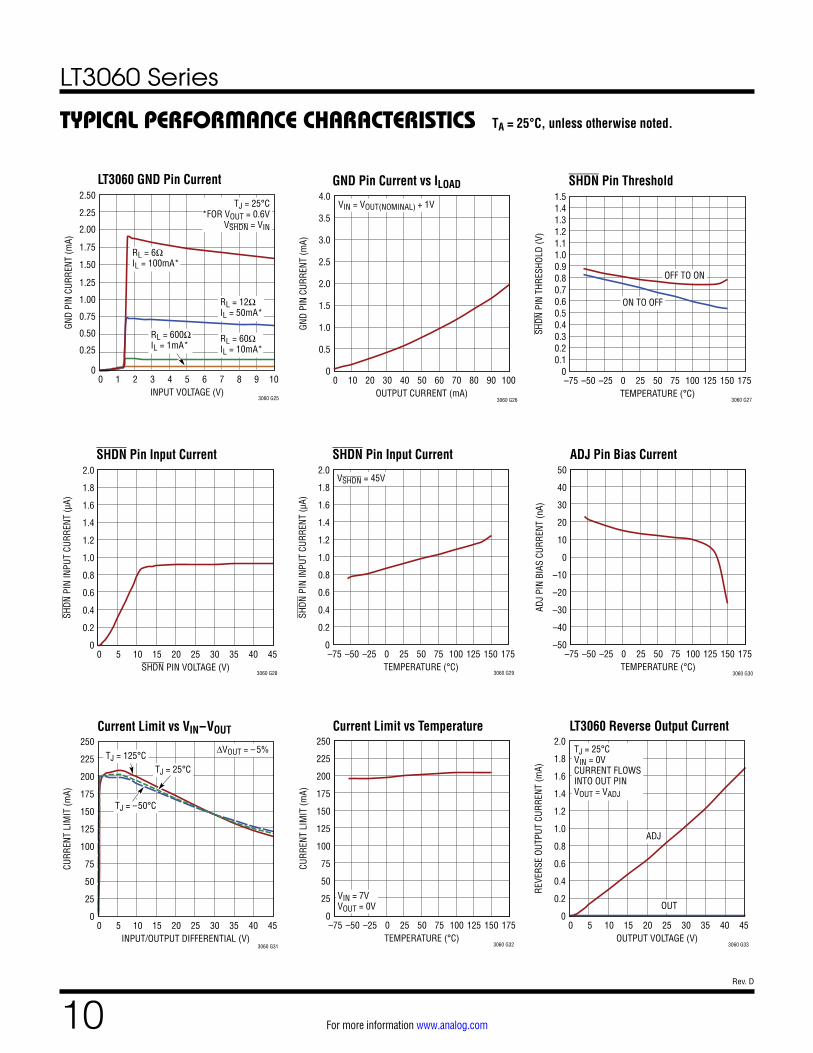
TYPICAL PERFORMANCE CHARACTERISTICS
TEMPERATURE (°C)–75
0
QUIE
SCEN
T CU
RREN
T (µ
A)
50
60
70
40
30
20
10
80
–50 75 100 125 150 175–25 0 25
3060 G04
50
VIN = 6V, VSHDN = VINRL = ∞ (120k FOR LT3060)IL = 0 (5µA FOR LT3060)
LT3060
VSHDN = 0V
LT3060-1.2/-1.5/-1.8/-2.5/-3.3/-5
Quiescent Current LT3060-1.2 Output Voltage LT3060-1.5 Output Voltage
LT3060-1.8 Output Voltage LT3060-2.5 Output Voltage LT3060-3.3 Output Voltage
TA = 25°C, unless otherwise noted.
TEMPERATURE (°C)–75
1.176
OUTP
UT V
OLTA
GE (V
)
1.200
1.204
1.208
1.212
1.216
1.220
1.196
1.1921.1881.184
1.180
1.224
–50 75 100 125 150 175–25 0 25
3060 G05
50
IL = 1mA
TEMPERATURE (°C)–75
1.470
OUTP
UT V
OLTA
GE (V
)
1.500
1.505
1.510
1.515
1.520
1.525
1.495
1.4901.4851.480
1.475
1.530
–50 75 100 125 150 175–25 0 25
3060 G06
50
IL = 1mA
TEMPERATURE (°C)–75
1.764
OUTP
UT V
OLTA
GE (V
)
1.800
1.806
1.812
1.818
1.824
1.830
1.794
1.7881.7821.776
1.770
1.836
–50 75 100 125 150 175–25 0 25
3060 G07
50
IL = 1mA
TEMPERATURE (°C)–75
2.45
OUTP
UT V
OLTA
GE (V
)
2.49
2.50
2.51
2.52
2.53
2.54
2.48
2.47
2.46
2.55
–50 75 100 125 150 175–25 0 25
3060 G08
50
IL = 1mA
TEMPERATURE (°C)–75
3.234
OUTP
UT V
OLTA
GE (V
)
3.300
3.311
3.322
3.333
3.344
3.355
3.289
3.2783.2673.256
3.245
3.366
–50 75 100 125 150 175–25 0 25
3060 G09
50
IL = 1mA

LT3060 Series
8Rev. D
For more information www.analog.com
TYPICAL PERFORMANCE CHARACTERISTICS TA = 25°C, unless otherwise noted.
TEMPERATURE (°C)–75
0.588
ADJ
PIN
VOLT
AGE
(V)
0.600
0.602
0.604
0.606
0.608
0.610
0.598
0.5960.5940.592
0.590
0.612
–50 75 100 125 150 175–25 0 25
3060 G11
50
IL = 1mAVIN = 2.1V
LT3060 ADJ Pin Voltage
0 1 2 7 8 9 103 4 5 6INPUT VOLTAGE (V)
0
QUIE
SCEN
T CU
RREN
T (µ
A)
100
125
150
175
75
50
25
200
3060 G15
TJ = 25°CRL = ∞VOUT = 2.5V
VSHDN = 0V
VSHDN = VIN
LT3060-2.5 Quiescent Current
LT3060-5 Output Voltage LT3060-15 Output Voltage
TEMPERATURE (°C)–75
4.90
OUTP
UT V
OLTA
GE (V
)
4.98
5.00
5.02
5.04
5.06
5.08
4.96
4.94
4.92
5.10
–50 75 100 125 150 175–25 0 25
3060 G10
50
IL = 1mA
LT3060-1.2 Quiescent Current
INPUT VOLTAGE (V)0 1
0
QUIE
SCEN
T CU
RREN
T (µ
A)
100
125
150
175
75
50
25
200
2 7 8 9 103 4 5
3060 G12
6
TJ = 25°CRL = ∞VOUT = 1.2V
VSHDN = 0V
VSHDN = VIN
LT3060-1.5 Quiescent Current
0 1 2 7 8 9 103 4 5 6INPUT VOLTAGE (V)
0
QUIE
SCEN
T CU
RREN
T (µ
A)
100
125
150
175
75
50
25
200
3060 G13
TJ = 25°CRL = ∞VOUT = 1.5V
VSHDN = 0V
VSHDN = VIN
LT3060-1.8 Quiescent Current
0 1 2 7 8 9 103 4 5 6INPUT VOLTAGE (V)
0
QUIE
SCEN
T CU
RREN
T (µ
A)
100
125
150
175
75
50
25
200
3060 G14
TJ = 25°CRL = ∞VOUT = 1.8V
VSHDN = 0V
VSHDN = VIN
LT3060-3.3 Quiescent Current
0 1 2 7 8 9 103 4 5 6INPUT VOLTAGE (V)
0
QUIE
SCEN
T CU
RREN
T (µ
A)
100
125
150
175
75
50
25
200
3060 G16
TJ = 25°CRL = ∞VOUT = 3.3V
VSHDN = 0V
VSHDN = VIN
LT3060-5 Quiescent Current
0 1 2 7 8 9 103 4 5 6INPUT VOLTAGE (V)
0
QUIE
SCEN
T CU
RREN
T (µ
A)
100
125
150
175
75
50
25
200
3060 G17
TJ = 25°CRL = ∞VOUT = 5V
VSHDN = 0V
VSHDN = VIN
TEMPERATURE (°C)–75
14.70
OUTP
UT V
OLTA
GE (V
)
15.00
15.05
15.1015.15
15.20
15.25
14.95
14.90
14.80
14.85
14.75
15.30
–50 75 100 125 150 175–25 0 25
3060 G10a
50
IL = 1mA

LT3060 Series
9Rev. D
For more information www.analog.com
INPUT VOLTAGE (V)0
0
QUIE
SCEN
T CU
RREN
T (µ
A)
70
60
50
40
30
20
10
80
5 30 35 40 4510 15 20
3060 G18
25
TJ = 25°CRL = 120k
VOUT = 0.6V
VSHDN = VIN
VSHDN = 0
LT3060 Quiescent CurrentLT3060-15 Quiescent Current
INPUT VOLTAGE (V)0
0
GND
PIN
CURR
ENT
(mA)
2.25
2.00
1.75
1.50
1.25
1.00
0.75
0.50
0.25
2.50
1 6 7 8 9 102 3 4
3060 G22
5
TJ = 25°C*FOR VOUT = 2.5V
VSHDN = VIN
RL = 25ΩIL = 100mA*
RL = 50ΩIL = 50mA*
RL = 250ΩIL = 10mA*
RL = 2.5kIL = 1mA*
LT3060-2.5 GND Pin Current
TYPICAL PERFORMANCE CHARACTERISTICS TA = 25°C, unless otherwise noted.
LT3060-1.2 GND Pin Current
INPUT VOLTAGE (V)0
0
GND
PIN
CURR
ENT
(mA)
2.25
2.00
1.75
1.50
1.25
1.00
0.75
0.50
0.25
2.50
1 6 7 8 9 102 3 4
3060 G19
5
TJ = 25°C*FOR VOUT = 1.2V
VSHDN = VIN
RL = 12ΩIL = 100mA*
RL = 24ΩIL = 50mA*
RL = 120ΩIL = 10mA*
RL = 1.2kIL = 1mA*
LT3060-1.5 GND Pin Current
INPUT VOLTAGE (V)0
0
GND
PIN
CURR
ENT
(mA)
2.25
2.00
1.75
1.50
1.25
1.00
0.75
0.50
0.25
2.50
1 6 7 8 9 102 3 4
3060 G20
5
TJ = 25°C*FOR VOUT = 1.5V
VSHDN = VIN
RL = 15ΩIL = 100mA*
RL = 30ΩIL = 50mA*
RL = 150ΩIL = 10mA*
RL = 1.5kIL = 1mA*
LT3060-1.8 GND Pin Current
INPUT VOLTAGE (V)0
0
GND
PIN
CURR
ENT
(mA)
2.25
2.00
1.75
1.50
1.25
1.00
0.75
0.50
0.25
2.50
1 6 7 8 9 102 3 4
3060 G21
5
TJ = 25°C*FOR VOUT = 1.8V
VSHDN = VIN
RL = 18ΩIL = 100mA*
RL = 36ΩIL = 50mA*
RL = 180ΩIL = 10mA*
RL = 1.8kIL = 1mA*
LT3060-3.3 GND Pin Current
INPUT VOLTAGE (V)0
0
GND
PIN
CURR
ENT
(mA)
2.25
2.00
1.75
1.50
1.25
1.00
0.75
0.50
0.25
2.50
1 6 7 8 9 102 3 4
3060 G23
5
TJ = 25°C*FOR VOUT = 3.3V
VSHDN = VIN
RL = 33ΩIL = 100mA*
RL = 66ΩIL = 50mA*
RL = 330ΩIL = 10mA*
RL = 3.3kIL = 1mA*
LT3060-5 GND Pin Current LT3060-15 GND Pin Current
0 5 10 35 40 4515 20 25 30INPUT VOLTAGE (V)
0
QUIE
SCEN
T CU
RREN
T (µ
A)
100
125
150
175
75
50
25
200
3060 G17a
TJ = 25°CRL = ∞VOUT = 15V
VSHDN = 0V
VSHDN = VIN
INPUT VOLTAGE (V)0
0
GND
PIN
CURR
ENT
(mA)
2.25
2.00
1.75
1.50
1.25
1.00
0.75
0.50
0.25
2.50
6 7 8 9 1021 3 4
3060 G24
5
TJ = 25°C*FOR VOUT = 5V
VSHDN = VIN
RL = 50ΩIL = 100mA*
RL = 100ΩIL = 50mA*
RL = 500ΩIL = 10mA*
RL = 5kIL = 1mA*
0 5 10 35 40 4515 20 25 30INPUT VOLTAGE (V)
0
QUIE
SCEN
T CU
RREN
T (m
A)
1.50
1.25
1.75
2.00
2.25
1.00
0.75
0.50
0.25
2.50
3060 G24a
TJ = 25°C*FOR VOUT = 15V
VSHDN = VIN
RL = 150ΩIL = 100mA*
RL = 300ΩIL = 50mA*
RL = 1.5kIL = 10mA*
RL = 15kIL = 1mA*
LT3060 Series
10Rev. D
For more information www.analog.com
SHDN Pin Input Current
TEMPERATURE (°C)–75
0
SHDN
PIN
INPU
T CU
RREN
T (µ
A)
1.4
1.6
1.8
1.2
1.0
0.8
0.4
0.6
0.2
2.0
–50 75 100 125 150 175–25 0 25
3060 G29
50
VSHDN = 45V
ADJ Pin Bias Current
TEMPERATURE (°C)–75
–50
ADJ
PIN
BIAS
CUR
RENT
(nA)
20
30
40
10
0
–10
–30
–20
–40
50
–50 75 100 125 150 175–25 0 25
3060 G30
50
Current Limit vs VIN–VOUT
INPUT/OUTPUT DIFFERENTIAL (V)0
0
CURR
ENT
LIM
IT (m
A)
225
150
175
200
125
100
50
75
25
250
5 30 35 40 4510 15 20
3060 G31
25
∆VOUT = – 5%
TJ = 25°CTJ = 125°C
TJ = –50°C
6-PHASE4-PHASE3-PHASE2-PHASE1-PHASE
Current Limit vs Temperature
TEMPERATURE (°C)–75
0
CURR
ENT
LIM
IT (m
A) 175
200
225
150
125
100
50
75
25
250
–50 75 100 125 150 175–25 0 25
3060 G32
50
VIN = 7VVOUT = 0V
LT3060 Reverse Output Current
OUTPUT VOLTAGE (V)0
0
REVE
RSE
OUTP
UT C
URRE
NT (m
A)
1.4
1.6
1.8
1.2
1.0
0.8
0.4
0.6
0.2
2.0
5 30 35 40 4510 15 20
3060 G33
25
ADJ
OUT
TJ = 25°CVIN = 0VCURRENT FLOWSINTO OUT PINVOUT = VADJ
TYPICAL PERFORMANCE CHARACTERISTICS
SHDN Pin Threshold
TEMPERATURE (°C)–75
0
SHDN
PIN
THR
ESHO
LD (V
)
0.70.80.91.01.11.21.31.4
0.60.50.4
0.20.3
0.1
1.5
–50 75 100 125 150 175–25 0 25
3060 G27
50
ON TO OFF
OFF TO ON
SHDN Pin Input Current
SHDN PIN VOLTAGE (V)0
0
SHDN
PIN
INPU
T CU
RREN
T (µ
A)
1.4
1.6
1.8
1.2
1.0
0.8
0.4
0.6
0.2
2.0
5 30 35 40 4510 15 20
3060 G28
25
TA = 25°C, unless otherwise noted.
GND Pin Current vs ILOAD
OUTPUT CURRENT (mA)0
0
GND
PIN
CURR
ENT
(mA)
3.5
3.0
2.5
2.0
1.0
1.5
0.5
4.0
10 60 70 80 90 10020 30 40
3060 G26
50
VIN = VOUT(NOMINAL) + 1V
INPUT VOLTAGE (V)0
0
GND
PIN
CURR
ENT
(mA)
2.25
2.00
1.75
1.50
1.25
1.00
0.75
0.50
0.25
2.50
1 6 7 8 9 102 3 4
3060 G25
5
TJ = 25°C*FOR VOUT = 0.6V
VSHDN = VIN
RL = 6ΩIL = 100mA*
RL = 12ΩIL = 50mA*
RL = 60ΩIL = 10mA*
RL = 600ΩIL = 1mA*
LT3060 GND Pin Current

LT3060 Series
11Rev. D
For more information www.analog.com
Reverse Output Current
TEMPERATURE (°C)–75
0
REVE
RSE
OUTP
UT C
URRE
NT (µ
A)
35
40
45
30
25
20
10
15
5
50
–50 75 100 125 150 175–25 0 25
3060 G35
50
VIN = 0V, VOUT = VADJ = 1.2V (LT3060)VOUT = 1.2V (LT3060-1.2)VOUT = 1.5V (LT3060-1.5)VOUT = 1.8V (LT3060-1.8)VOUT = 2.5V (LT3060-2.5)VOUT = 3.3V (LT3060-3.3)VOUT = 5V (LT3060-5)VOUT = 15V (LT3060-15)
OUT (LT3060)
ADJ (LT3060)
OUT (LT3060-1.2/-1.5/-1.8/2.5/-3.3/-5/-15)
LT3060-1.2/-1.5/-1.8/-2.5/-3.3/-5 /-15 Reverse Output Current
OUTPUT VOLTAGE (V)0
0
REVE
RSE
OUTP
UT C
URRE
NT (µ
A)
250
150
200
100
50
350
300
5 30 35 40 4510 15 20
3060 G34
25
LT3060-1.2
LT3060-5
LT3060-15
LT3060-1.5
LT3060-1.8
LT3060-2.5
LT3060-3.3
TJ = 25°CVIN = 0V
TYPICAL PERFORMANCE CHARACTERISTICS
Input Ripple Rejection
IL = 100mACREF/BYP = CFF = 0VIN = VOUT(NOMINAL) + 1.5V +50mVRMS RIPPLE
FREQUENCY (Hz)10
0
RIPP
LE R
EJEC
TION
(dB)
60
70
80
90
50
40
30
20
10
100
100 10M1k 10k 100k
3060 G36
1M
VOUT = 0.6V
COUT = 10µF
COUT = 2.2µF
VOUT = 5V
VOUT = 1.8VVOUT = 2.5VVOUT = 3.3VVOUT = 0.6V, COUT = 2.2µF
LT3060-5 Input Ripple Rejection LT3060-15 Input Ripple Rejection
FREQUENCY (Hz)10
0
RIPP
LE R
EJEC
TION
(dB)
60
70
80
90
50
40
30
20
10
100
100 10M1k 10k 100k
3060 G37
1M
IL = 100mAVOUT = 5VCOUT = 10µFVIN = 6V + 50mVRMS RIPPLE
CREF/BYP = CFF = 10nF
CREF/BYP = 10nF, CFF = 0
CREF/BYP = CFF = 0
Ripple Rejection vs Temperature
TEMPERATURE (°C)–75
0
RIPP
LE R
EJEC
TION
(dB)
90
80
70
60
40
50
30
20
10
100
–50 75 100 125 150 175–25 0 25
3060 G38
50
CREF/BYP = 10nF
CREF/BYP = 0
IL = 100mAVOUT = 0.6VVIN = 2.6V + 0.5VP-P RIPPLE AT f = 120Hz
Minimum Input Voltage
TEMPERATURE (°C)–75
0
MIN
IMUM
INPU
T VO
LTAG
E (V
)
1.4
1.6
1.8
2.0
1.2
1.0
0.8
0.4
0.6
0.2
2.2
–50 75 100 125 150 175–25 0 25
3060 G39
50
IL = 50mA
IL = 100mA
VSHDN = VIN
Load Regulation Load Regulation
TEMPERATURE (°C)–75
LOAD
REG
ULAT
ION
(mV)
5
0
–5
–10
–20
–15
–25–50 75 100 125 150 175–25 0 25
3060 G40
50
VIN = VOUT(NOMINAL) + 0.55V (LT3060-1.8/-2.5/-3.3/-5)VIN = 2.1V (LT3060/-1.2/-1.5)∆IL = 1mA TO 100mA
LT3060-5LT3060-3.3LT3060-2.5LT3060-1.8LT3060-1.5LT3060-1.2LT3060
TA = 25°C, unless otherwise noted.
FREQUENCY (Hz)10
0
RIPP
LE R
EJEC
TION
(dB)
60
70
80
90
50
40
30
20
10
100
100 10M1k 10k 100k
3060 G37a
1M
IL = 100mAVOUT = 15VCOUT = 10µFVIN = 16V + 50mVRMS RIPPLE
CREF/BYP = CFF = 10nF
CREF/BYP = 10nF, CFF = 0
CREF/BYP = CFF = 0
TEMPERATURE (°C)–75
LOAD
REG
ULAT
ION
(mV)
0
–5
–10
–15
–25
–30
–35
–40
–45
–20
–50–50 75 100 125 150 175–25 0 25
3060 G40a
50
VIN = VOUT(NOMINAL) + 0.55V∆IL = 1mA TO 100mA
LT3060-2.5
LT3060-5
LT3060-15

LT3060 Series
12Rev. D
For more information www.analog.com
RMS Output Noise vs Load Current vs CREF/BYP, CFF = 0
LOAD CURRENT (mA)0.010
OUTP
UT N
OISE
VOL
TAGE
(µV R
MS)
40
30
20
10
110
100
90
80
70
60
50
101 100
3060 G44
0.1
VOUT = 0.6VCOUT = 10µF CREF/BYP = 0
CREF/BYP = 10pF
CREF/BYP = 100pF
CREF/BYP = 1nF
CREF/BYP = 10nF
CREF/BYP = 100nF
TYPICAL PERFORMANCE CHARACTERISTICS
RMS Output Noise vs Feedforward Capacitor (CFF)
RMS Output Noise vs Feedforward Capacitor (CFF)
RMS Output Noise vs Load Current CREF/BYP = 10nF, CFF = 0
RMS Output Noise vs Load Current CREF/BYP = 10nF, CFF = 0
LOAD CURRENT (mA)0.010
OUTP
UT N
OISE
VOL
TAGE
(µV R
MS)
5040302010
170
120130140150160
110100
90807060
101 100
3060 G45
0.1
VOUT = 5V
VOUT = 3.3V
VOUT = 1.2V
VOUT = 2.5V
VOUT = 1.8V
VOUT = 1.5V
VOUT = 0.6V
f = 10Hz TO 100kHzCOUT = 10µFIFB-DIVIDER = 5µA
FEEDFORWARD CAPACITOR, CFF (F)10p
0
OUTP
UT N
OISE
VOL
TAGE
(µV R
MS)
10
120
70
80
90
100
110
60
50
40
30
20
1n 10n
3060 G46
100p
f = 10Hz TO 100kHzCREF/BYP = 10nFCOUT = 10µFIFB-DIVIDER = 5µAIL = 100mA
VOUT = 0.6V
VOUT = 5V
VOUT = 1.8V
VOUT = 1.5V
VOUT = 1.2V
VOUT = 2.5V
VOUT = 3.3V
TA = 25°C, unless otherwise noted.
Output Noise Spectral Density CREF/BYP = 0, CFF = 0
VOUT = 1.8VVOUT = 1.5VVOUT = 1.2VVOUT = 0.6V
VOUT = 15VVOUT = 5VVOUT = 3.3VVOUT = 2.5V
FREQUENCY (Hz)10
0.01OUTP
UT N
OISE
SPE
CTRA
L DE
NSIT
Y (µ
V/√H
z)
10
1
0.1
100
10k 100k100
3060 G41
1k
COUT = 10µFIL = 100mA
Output Noise Spectral Density vs CREF/BYP, CFF = 0
FREQUENCY (Hz)10
0.01OUTP
UT N
OISE
SPE
CTRA
L DE
NSIT
Y (µ
V/√H
z)
1
0.1
10
10k1k 100k
3060 G42
100
VOUT = 5V
CREF/BYP = 10nF
CREF/BYP = 1nF
VOUT = 0.6V
COUT = 10µFIL = 100mA
CREF/BYP = 100pF
Output Noise Spectral Density vs CFF, CREF/BYP = 10nF
FREQUENCY (Hz)10
0.01OUTP
UT N
OISE
SPE
CTRA
L DE
NSIT
Y (µ
V/√H
z)
1
0.1
10
10k1k 100k
3060 G43
100
CFF = 0
CFF = 100pF
CFF = 10nF
VOUT = 5VCOUT = 10µFIL = 100mA
CFF = 1nF
LOAD CURRENT (mA)0.010
OUTP
UT N
OISE
VOL
TAGE
(µV R
MS)
125100755025
350
250275300325
225200175150
101 100
3060 G45a
0.1
VOUT = 15V
VOUT = 5V
VOUT = 2.5V
VOUT = 0.6V
f = 10Hz TO 100kHzCOUT = 10µFIFB-DIVIDER = 5µA
FEEDFORWARD CAPACITOR, CFF (F)10p
0
OUTP
UT N
OISE
VOL
TAGE
(µV R
MS)
25
250
150
175
200
225
125
100
75
50
1n 10n
3060 G46a
100p
f = 10Hz TO 100kHzCREF/BYP = 10nFCOUT = 10µFIFB-DIVIDER = 5µAIL = 100mA
VOUT = 0.6V
VOUT = 15V
VOUT = 5V
VOUT = 2.5V

LT3060 Series
13Rev. D
For more information www.analog.com
LT3060-5 10Hz to 100kHz Output Noise, CREF/BYP = 10nF, CFF = 10nF
LT3060-5 Transient Response, CFF = 0
LT3060-5 Transient Response, CFF = 10nF
1ms/DIVCOUT = 10µFIL = 100mAVOUT = 5V
VOUT100µV/DIV
3060 G48100µs/DIVVIN = 6V
COUT = CIN = 10µFIFB-DIVIDER = 5µA
VOUT50mV/DIV
IOUT50mA/DIV
3060 G49
∆IOUT = 10mA TO 100mA
VOUT = 5V
20µs/DIVVIN = 6VCOUT = CIN = 10µFIFB-DIVIDER = 5µA
VOUT20mV/DIV
IOUT50mA/DIV
3060 G50
∆IOUT = 10mA TO 100mA
VOUT = 5V
LT3060-5 10Hz to 100kHz Output Noise, CREF/BYP = 10nF, CFF = 0
1ms/DIVCOUT = 10µFIL = 100mAVOUT = 5V
VOUT100µV/DIV
3060 G47
TYPICAL PERFORMANCE CHARACTERISTICS
LT3060-5 Transient Response Load Dump
SHDN Transient Response CREF/BYP = 0
SHDN Transient Response CREF/BYP = 10nF
2ms/DIVCOUT = CIN = 2.2µFCREF/BYP = CFF = 10nFIFB-DIVIDER = 5µA
VOUT10mV/DIV
VIN10V/DIV
3060 G51
VIN = 12V TO 45V
VOUT = 5V
4ms/DIV
VOUT2V/DIV
RL = 50Ω
REF/BYP500mV/DIV
SHDN1V/DIV
3060 G52
COUT = CIN = 2.2µFCFF = 0
4ms/DIV
VOUT2V/DIV
RL = 50Ω
REF/BYP500mV/DIV
SHDN1V/DIV
3060 G53
COUT = CIN = 2.2µFCFF = 0
TA = 25°C, unless otherwise noted.

LT3060 Series
14Rev. D
For more information www.analog.com
Start-Up Time vs REF/BYP Capacitor
REF/BYP CAPACITOR (F)10p
0.01
STAR
T-UP
TIM
E (m
s)
10
1
0.1
100
10n 100n100p
3060 G54
1n
CFF = 0
Start-Up Time vs CFF
LT3060-5
LT3060-15
FEEDFORWARD CAPACITOR, CFF (F)10p
STAR
T-UP
TIM
E (m
s)
10n1n 100n
3060 G55
100p
CREF/BYP = 0IFB-DIVIDER = 5µA
0.01
1
10
1000
100
0.1
LT3060-3.3
LT3060-1.2LT3060-1.5
LT3060-1.8
LT3060-2.5
TYPICAL PERFORMANCE CHARACTERISTICS TA = 25°C, unless otherwise noted.

LT3060 Series
15Rev. D
For more information www.analog.com
PIN FUNCTIONSREF/BYP (Pin 1/Pin 8): Reference/Bypass. Connecting a single capacitor from this pin to GND bypasses the LT3060’s reference noise and soft-starts the reference. A 10nF bypass capacitor typically reduces output voltage noise to 30µVRMS in a 10Hz to 100kHz bandwidth. Soft-start time is directly proportional to the REF/BYP capacitor value. If the LT3060 is placed in shutdown, REF/BYP is actively pulled low by an internal device to reset soft-start. If low noise or soft-start performance is not required, this pin must be left floating (unconnected). Do not drive this pin with any active circuitry.
ADJ (Pin 2/Pin 7): Adjust. This pin is the error ampli-fier’s inverting terminal. It’s typical bias current of 15nA flows out of the pin (see curve of ADJ Pin Bias Current vs Temperature in the Typical Performance Characteristics section). The ADJ pin voltage is 600mV referenced to GND.
Connecting a capacitor from ADJ to OUT reduces output noise and improves transient response for output voltages greater than 600mV. See the Applications Information sec-tion for calculating the value of the feedforward capacitor. For fixed voltage versions of the LT3060, if low noise and fast transient response is not required, this pin must be left floating (unconnected).
OUT (Pins 3, 4/Pin 6): Output. These pin(s) supply power to the load. Stability requirements demand a minimum 2.2µF ceramic output capacitor to prevent oscillations. Large load transient applications require larger output capaci-tors to limit peak voltage transients. See the Applications Information section for details on transient response and reverse output characteristics. Permissible output voltage range is 600mV to 44.5V.
IN (Pins 5, 6/Pin 5): Input. These pin(s) supply power to the device. The LT3060 requires a local IN bypass capacitor if it is located more than six inches from the main input filter capacitor. In general, battery output impedance rises with frequency, so adding a bypass capacitor in battery-powered circuits is advisable.
An input bypass capacitor in the range of 1µF to 10µF suffices. The LT3060 withstands reverse voltages on the IN pin with respect to its GND and OUT pins. In a reversed input situation, such as a battery plugged in backwards, the LT3060 behaves as if a large resistor is in series with its input. Limited reverse current flows into the LT3060 and no reverse voltage appears at the load. The device protects itself and the load.
SHDN (Pin 7/Pin 1): Shutdown. Pulling the SHDN pin low puts the LT3060 into a low power state and turns the output off. Drive the SHDN pin with either logic or an open collector/drain with a pull-up resistor. The resistor supplies the pull-up current to the open collector/drain logic, normally several microamperes, and the SHDN pin current, typically less than 3µA. If unused, connect the SHDN pin to IN. The LT3060 does not function if the SHDN pin is not connected. The SHDN pin cannot be driven below GND unless tied to the IN pin. If the SHDN pin is driven below GND while IN is powered, the output may turn on. SHDN pin logic cannot be referenced to a negative supply voltage.
GND (Pin 8, Exposed Pad Pin 9/Pins 2, 3, 4): Ground. For the adjustable LT3060, connect the bottom of the ex-ternal resistor divider that sets the output voltage directly to GND for optimum regulation. For the DFN package, tie exposed pad Pin 9 directly to Pin 8 and the PCB ground. This exposed pad provides enhanced thermal performance with its connection to the PCB ground. See the Applica-tions Information section for thermal considerations and calculating junction temperature.
(DC8/TS8)

LT3060 Series
16Rev. D
For more information www.analog.com
The LT3060 series are micropower, low noise, low drop-out voltage, 100mA linear regulators with shutdown. The devices supply up to 100mA at a typical dropout voltage of 300mV and operate over a 1.6V to 45V input range.
A single external capacitor provides programmable low noise reference performance and output soft-start func-tionality. For example, connecting a 10nF capacitor from the REF/BYP pin to GND lowers output noise to 30µVRMS over a 10Hz to 100kHz bandwidth. This capacitor also soft-starts the reference and prevents output voltage overshoot at turn-on.
The LT3060’s quiescent current is merely 40μA for the adjustable version and 45µA for the fixed voltage versions, while providing fast transient response with a minimum low ESR 2.2μF ceramic output capacitor. In shutdown, quiescent current is less than 1μA and the reference soft-start capacitor is reset.
The LT3060 regulators optimize stability and transient response with low ESR, ceramic output capacitors. The regulators do not require the addition of ESR as is com-mon with other regulators. The LT3060 adjustable version typically provides 0.1% line regulation and 0.03% load regulation. For fixed voltage versions, load regulation is slightly increased due to 20mΩ of typical resistance in series with the output. Curves of load regulation appear in the Typical Performance Characteristics section.
Internal protection circuitry includes reverse-battery pro-tection, reverse-output protection, reverse-current protec-tion, current limit with foldback and thermal shutdown.
This “bullet-proof” protection set makes it ideal for use in battery-powered systems. In battery backup applications where the output is held up by a backup battery and the input is pulled to ground, the LT3060 acts like it has a di-ode in series with its output and prevents reverse current flow. Additionally, in dual supply applications where the regulator load is returned to a negative supply, the output can be pulled below ground by as much as 45V and the device still starts normally and operates.
APPLICATIONS INFORMATION
3060 F01
IN
SHDN
OUT
ADJ
GND REF/BYP
LT3060VIN
VOUT
R2
R1
Figure 1. Adjustable Operation
VOUT = 0.6V 1+R2R1
⎛
⎝⎜
⎞
⎠⎟ – IADJ •R2( )
VADJ = 0.6V
IADJ = 15nA at 25ºC
OUTPUTRANGE = 0.6V to 44.5V
Adjustable Operation
The LT3060 adjustable version has an output voltage range of 0.6V to 44.5V. The output voltage is set by the ratio of two external resistors, as shown in Figure 1. The device servos the output to maintain the ADJ pin voltage at 0.6V referenced to ground. The current in R1 is then equal to 0.6V/R1, and the current in R2 is the current in R1 minus the ADJ pin bias current. The ADJ pin bias current, 15nA at 25°C, flows from the ADJ pin through R1 to GND. Calculate the output voltage using the formula in Figure 1. The value of R1 should be no greater than 124k to provide a minimum 5µA load current so that errors in the output voltage, caused by the ADJ pin bias current, are minimized. Note that in shutdown, the output is turned off and the divider current is zero. Curves of ADJ Pin Voltage vs Temperature and ADJ Pin Bias Cur-rent vs Temperature appear in the Typical Performance Characteristics section.
The adjustable device is tested and specified with the ADJ pin tied to the OUT pin, yielding VOUT = 0.6V. Specifications for output voltages greater than 0.6V are proportional to the ratio of the desired output voltage to 0.6V: VOUT/0.6V. For example, load regulation for an output current change of 1mA to 100mA is 0.2mV (typical) at VOUT = 0.6V. At VOUT = 12V, load regulation is:
12V0.6V
• (0.2mV)= 4mV

LT3060 Series
17Rev. D
For more information www.analog.com
Table 1 shows 1% resistor divider values for some common output voltages with a resistor divider current of about 5µA.
Table 1. Output Voltage Resistor Divider ValuesVOUT (V)
R1 (kΩ)
R2 (kΩ)
1.2 118 118
1.5 121 182
1.8 124 249
2.5 115 365
3 124 499
3.3 124 562
5 115 845
12 124 2370
15 124 3010
Bypass Capacitance, Output Voltage Noise and Transient Response
The LT3060 regulators provide low output voltage noise over the 10Hz to 100kHz bandwidth while operating at full load with the addition of a reference bypass capacitor (CREF/BYP) from the REF/BYP pin to GND. A good quality, low leakage capacitor is recommended. This capacitor bypasses the internal reference of the regulator, provid-ing a low frequency noise pole. With the use of 10nF for CREF/BYP, the output voltage noise decreases to as low as 30µVRMS when the output voltage is set for 0.6V. For higher output voltages (generated by using a feedback resistor divider), the output voltage noise gains up accordingly when using CREF/BYP by itself.
To lower the output voltage noise for higher output volt-ages, include a feedforward capacitor (CFF) from VOUT to the ADJ pin. A good quality, low leakage capacitor is recommended. This capacitor bypasses the error amplifier of the regulator, providing a low frequency noise pole. With the use of 10nF for both CFF and CREF/BYP, output voltage noise decreases to 30µVRMS when the output voltage is set to 5V by a 5µA feedback resistor divider. If the current in the feedback resistor divider is doubled, CFF must also be doubled to achieve equivalent noise performance.
Higher values of output voltage noise are often measured if care is not exercised with regard to circuit layout and testing. Crosstalk from nearby traces induces unwanted noise onto the LT3060’s output. Power supply ripple rejec-tion must also be considered. The LT3060 regulators do not have unlimited power supply rejection and will pass a small portion of the input noise through to the output.
Using a feedforward capacitor (CFF) from VOUT to the ADJ pin has the added benefit of improving transient response for output voltages greater than 0.6V. With no feedforward capacitor, the settling time will increase as the output voltage is raised above 0.6V. Use the equation in Figure 2 to determine the minimum value of CFF to achieve a transient response that is similar to 0.6V output voltage performance regardless of the chosen output voltage (see Figure 3 and Transient Response in the Typical Perf-ormance Characteristics section).
Figure 2. Feedforward Capacitor for Fast Transient Response
Figure 3. Transient Response vs Feedforward Capacitor
APPLICATIONS INFORMATION
3060 F02
IN
SHDN
OUT
ADJ
GND REF/BYP
LT3060VIN
VOUT
CREF/BYP
CFF COUTR2
R1
100µs/DIV
VOUT = 5VCOUT = 10µFIFB-DIVIDER = 5µA
0
1nF
10nF
LOAD CURRENT100mA/DIV
FEED
FORW
ARD
CAPA
CITO
R, C
FF
100pF
3060 F03
VOUT
50mV/DIV
CFF ≥4.7nF5µA
• IFB−DIVIDER( )
IFB−DIVIDER =VOUTR1+R2

LT3060 Series
18Rev. D
For more information www.analog.com
During start-up, the internal reference soft-starts if a reference bypass capacitor is present. Regulator start-up time is directly proportional to the size of the bypass capacitor, slowing to 6ms with a 10nF bypass capacitor (See Start-up Time vs REF/BYP Capacitor in the Typical Performance Characteristics section). The reference by-pass capacitor is actively pulled low during shutdown to reset the internal reference.
Start-up time is also affected by the use of a feedforward capacitor. Start-up time is directly proportional to the size of the feedforward capacitor and output voltage, and is inversely proportional to the feedback resistor divider current, slowing to 15ms with a 4.7nF feedforward ca-pacitor and a 10µF output capacitor for an output voltage set to 5V by a 5µA feedback resistor divider.
Output Capacitance
The LT3060 regulators are stable with a wide range of output capacitors. The ESR of the output capacitor af-fects stability, most notably with small capacitors. Use a minimum output capacitor of 2.2µF with an ESR of 3Ω or less to prevent oscillations. If a feedforward capacitor is used with output voltages set for greater than 24V, use a minimum output capacitor of 4.7µF. The LT3060 is a micropower device and output load transient response is a function of output capacitance. Larger values of output capacitance decrease the peak deviations and provide improved transient response for larger load current
changes. Bypass capacitors, used to decouple individual components powered by the LT3060, increase the effec-tive output capacitor value. For applications with large load current transients, a low ESR ceramic capacitor in parallel with a bulk tantalum capacitor often provides an optimally damped response.
Give extra consideration to the use of ceramic capacitors. Manufacturers make ceramic capacitors with a variety of dielectrics, each with different behavior across tempera-ture and applied voltage. The most common dielectrics are specified with EIA temperature characteristic codes of Z5U, Y5V, X5R and X7R. The Z5U and Y5V dielectrics provide high C-V products in a small package at low cost , but exhibit strong voltage and temperature coefficients, as shown in Figures 4 and 5. When used with a 5V regulator, a 16V 10µF Y5V capacitor can exhibit an effective value as low as 1µF to 2µF for the DC bias voltage applied, and over the operating temperature range. The X5R and X7R dielectrics yield much more stable characteristics and are more suitable for use as the output capacitor.
The X7R type works over a wider temperature range and has better temperature stability, while the X5R is less expensive and is available in higher values. Care still must be exercised when using X5R and X7R ca-pacitors; the X5R and X7R codes only specify operating temperature range and maximum capacitance change over temperature. Capacitance change due to DC bias with X5R and X7R capacitors is better than Y5V and Z5U
Figure 4. Ceramic Capacitor DC Bias Characteristics
APPLICATIONS INFORMATION
DC BIAS VOLTAGE (V)
CHAN
GE IN
VAL
UE (%
)
3060 F04
20
0
–20
–40
–60
–80
–1000 4 8 102 6 12 14
X5R
Y5V
16
BOTH CAPACITORS ARE 16V,1210 CASE SIZE, 10µF
TEMPERATURE (°C)–50
40
20
0
–20
–40
–60
–80
–10025 75
3060 F05
–25 0 50 100 125
Y5V
CHAN
GE IN
VAL
UE (%
) X5R
BOTH CAPACITORS ARE 16V,1210 CASE SIZE, 10µF
Figure 5. Ceramic Capacitor Temperature Characteristics

LT3060 Series
19Rev. D
For more information www.analog.com
4ms/DIV3060 F06
VOUT500µV/DIV
VOUT = 0.6VCOUT = 10µFCREF/BYP = 10nFILOAD = 100mA
Figure 6. Noise Resulting from Tapping on a Ceramic Capacitor
APPLICATIONS INFORMATIONcapacitors, but can still be significant enough to drop capacitor values below appropriate levels. Capacitor DC bias characteristics tend to improve as component case size increases, but expected capacitance at operating voltage should be verified.
Voltage and temperature coefficients are not the only sources of problems. Some ceramic capacitors have a piezoelectric response. A piezoelectric device generates voltage across its terminals due to mechanical stress, similar to the way a piezoelectric accelerometer or mi-crophone works. For a ceramic capacitor, the stress is induced by vibrations in the system or thermal transients. The resulting voltages produced cause appreciable amounts of noise. A ceramic capacitor produced the trace in Figure 6 in response to light tapping from a pencil. Similar vibration induced behavior can masquerade as increased output voltage noise.
allowing the regulator to supply large output currents. With a high input voltage, a problem can occur wherein the removal of an output short will not allow the output to recover. Other regulators, such as the LT1083/LT1084/LT1085 family and LT1764A also exhibit this phenomenon, so it is not unique to the LT3060. The problem occurs with a heavy output load when the input voltage is high and the output voltage is low. Common situations are: (1) immediately after the removal of a short-circuit or (2) if the shutdown pin is pulled high after the input voltage is already turned on. The load line intersects the output current curve at two points creating two stable output operating points for the regulator. With this double intersection, the input power supply needs to be cycled down to zero and brought up again for the output to recover.
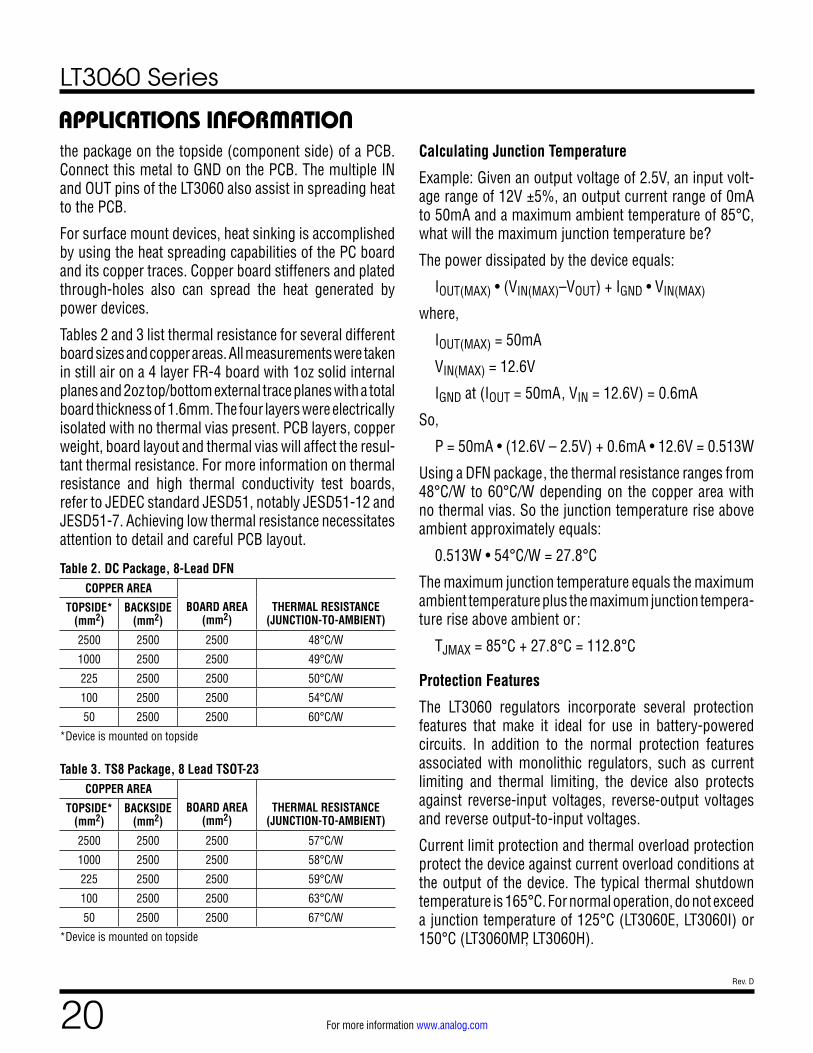
Thermal Considerations
The power handling capability of the device will be limited by the maximum rated junction temperature (125°C for LT3060E, LT3060I or 150°C for LT3060MP, LT3060H). Two components comprise the power dissipated by the device:
1. Output current multiplied by the input/output voltage differential: IOUT • (VIN–VOUT), and
2. GND pin current multiplied by the input voltage: IGND • VIN
GND pin current is determined using the GND Pin Current curves in the Typical Performance Characteristics section. Power dissipation equals the sum of the two components listed above.
The LT3060 regulators have internal thermal limiting that protects the device during overload conditions. For continu-ous normal conditions, the maximum junction temperature of 125°C (E-grade, I-grade) or 150°C (MP-grade, H-grade) must not be exceeded. Carefully consider all sources of thermal resistance from junction-to-ambient including other heat sources mounted in proximity to the LT3060.
The underside of the LT3060 DFN package has exposed metal (1mm2) from the lead frame to the die attachment. The package allows heat to directly transfer from the die junction to the printed circuit board metal to control maxi-mum operating junction temperature. The dual-in-line pin arrangement allows metal to extend beyond the ends of
Overload Recovery
Like many IC power regulators, the LT3060 has safe operating area protection. The safe operating area protec-tion decreases current limit as input-to-output voltage increases, and keeps the power transistor inside a safe operating region for all values of input-to-output voltage. The LT3060 provides some output current at all values of input-to-output voltage up to the specified 45V operational maximum.
When power is first applied, the input voltage rises and the output follows the input; allowing the regulator to start-up into very heavy loads. During start-up, as the input voltage is rising, the input-to-output voltage differential is small,
LT3060 Series
20Rev. D
For more information www.analog.com
the package on the topside (component side) of a PCB. Connect this metal to GND on the PCB. The multiple IN and OUT pins of the LT3060 also assist in spreading heat to the PCB.
For surface mount devices, heat sinking is accomplished by using the heat spreading capabilities of the PC board and its copper traces. Copper board stiffeners and plated through-holes also can spread the heat generated by power devices.
Tables 2 and 3 list thermal resistance for several different board sizes and copper areas. All measurements were taken in still air on a 4 layer FR-4 board with 1oz solid internal planes and 2oz top/bottom external trace planes with a total board thickness of 1.6mm. The four layers were electrically isolated with no thermal vias present. PCB layers, copper weight, board layout and thermal vias will affect the resul-tant thermal resistance. For more information on thermal resistance and high thermal conductivity test boards, refer to JEDEC standard JESD51, notably JESD51-12 and JESD51-7. Achieving low thermal resistance necessitates attention to detail and careful PCB layout.
Table 2. DC Package, 8-Lead DFNCOPPER AREA
BOARD AREA (mm2)
THERMAL RESISTANCE (JUNCTION-TO-AMBIENT)
TOPSIDE* (mm2)
BACKSIDE (mm2)
2500 2500 2500 48°C/W
1000 2500 2500 49°C/W
225 2500 2500 50°C/W
100 2500 2500 54°C/W
50 2500 2500 60°C/W
*Device is mounted on topside
Table 3. TS8 Package, 8 Lead TSOT-23COPPER AREA
BOARD AREA (mm2)
THERMAL RESISTANCE (JUNCTION-TO-AMBIENT)
TOPSIDE* (mm2)
BACKSIDE (mm2)
2500 2500 2500 57°C/W
1000 2500 2500 58°C/W
225 2500 2500 59°C/W
100 2500 2500 63°C/W
50 2500 2500 67°C/W
*Device is mounted on topside
Calculating Junction Temperature
Example: Given an output voltage of 2.5V, an input volt-age range of 12V ±5%, an output current range of 0mA to 50mA and a maximum ambient temperature of 85°C, what will the maximum junction temperature be?
The power dissipated by the device equals:
IOUT(MAX) • (VIN(MAX)–VOUT) + IGND • VIN(MAX)
where,
IOUT(MAX) = 50mA
VIN(MAX) = 12.6V
IGND at (IOUT = 50mA, VIN = 12.6V) = 0.6mA
So,
P = 50mA • (12.6V – 2.5V) + 0.6mA • 12.6V = 0.513W
Using a DFN package, the thermal resistance ranges from 48°C/W to 60°C/W depending on the copper area with no thermal vias. So the junction temperature rise above ambient approximately equals:
0.513W • 54°C/W = 27.8°C
The maximum junction temperature equals the maximum ambient temperature plus the maximum junction tempera-ture rise above ambient or:
TJMAX = 85°C + 27.8°C = 112.8°C
Protection Features
The LT3060 regulators incorporate several protection features that make it ideal for use in battery-powered circuits. In addition to the normal protection features associated with monolithic regulators, such as current limiting and thermal limiting, the device also protects against reverse-input voltages, reverse-output voltages and reverse output-to-input voltages.
Current limit protection and thermal overload protection protect the device against current overload conditions at the output of the device. The typical thermal shutdown temperature is 165°C. For normal operation, do not exceed a junction temperature of 125°C (LT3060E, LT3060I) or 150°C (LT3060MP, LT3060H).
APPLICATIONS INFORMATION

LT3060 Series
21Rev. D
For more information www.analog.com
APPLICATIONS INFORMATIONThe LT3060 IN pin withstands reverse voltages up to 50V. The device limits current flow to less than 300µA (typi-cally less than 50µA) and no negative voltage appears at OUT. The device protects both itself and the load against batteries that are plugged in backwards.
The SHDN pin cannot be driven below GND unless tied to the IN pin. If the SHDN pin is driven below GND while IN is powered, the output may turn on. SHDN pin logic cannot be referenced to a negative supply voltage.
The LT3060 incurs no damage if its output is pulled be-low ground. If the input is left open-circuit or grounded, the output can be pulled below ground by 50V. No cur-rent flows through the pass transistor from the output. However, current flows in (but is limited by) the resistor divider that sets the output voltage. Current flows from the bottom resistor in the divider and from the ADJ pin’s internal clamp through the top resistor in the divider to the external circuitry pulling OUT below ground. If the input is powered by a voltage source, the output sources current equal to its current limit capability and the LT3060 protects itself by thermal limiting. In this case, grounding the SHDN pin turns off the device and stops the output from sourcing current.
The LT3060 incurs no damage if the ADJ pin is pulled above or below ground by less than 50V. For the adjust-able version, if the input is left open-circuit or grounded, the ADJ pin performs like a large resistor (typically 30k) in series with a diode when pulled below ground, and like 30k in series with two diodes when pulled above ground.
In circuits where a backup battery is required, several different input /output conditions can occur. The output voltage may be held up while the input is either pulled to ground, pulled to some intermediate voltage or left open-circuit. Current flow back into the output follows the curve shown in Figures 7 and 8.
If the LT3060’s IN pin is forced below the OUT pin or the OUT pin is pulled above the IN pin, input current typically drops to less than 1µA. This occurs if the LT3060 input is connected to a discharged (low voltage) battery and either a backup battery or a second regulator holds up the output. The state of the SHDN pin has no effect on the reverse current if the output is pulled above the input.
OUTPUT VOLTAGE (V)0
0
REVE
RSE
OUTP
UT C
URRE
NT (m
A)
1.4
1.6
1.8
1.2
1.0
0.8
0.4
0.6
0.2
2.0
5 30 35 40 4510 15 20
3060 F07
25
ADJ
OUT
TJ = 25°CVIN = 0VCURRENT FLOWSINTO OUT PINVOUT = VADJ
Figure 7. LT3060 Reverse Output Current Figure 8. LT3060-1.2/-1.5/-1.8/-2.5/-3.3/-5/-15 Reverse Output Current
OUTPUT VOLTAGE (V)0
0
REVE
RSE
OUTP
UT C
URRE
NT (µ
A)
250
150
200
100
50
350
300
5 30 35 40 4510 15 20
3060 F08
25
LT3060-1.2
LT3060-5
LT3060-15
LT3060-1.5
LT3060-1.8
LT3060-2.5
LT3060-3.3
TJ = 25°CVIN = 0V

LT3060 Series
22Rev. D
For more information www.analog.com
TYPICAL APPLICATION
+IN
GND REF/BYPSHDN
OUT
ADJ
LT3060
IN
GND REF/BYPSHDN
OUT
ADJ
LT3060
VIN > 2.9V C12.2µF
R10.15Ω
R20.15Ω
R3200Ω
R4200Ω
C510nF
C41nF
C31nF
2.5V200mA
C24.7µF
R51k
3
2
7
4
6
SHDN
–
+
R81.91k1%
R61.74k1%
R7604Ω1%
R9604Ω1%
LT1637
3060 TA03
Paralleling of Regulators for Higher Output Current

LT3060 Series
23Rev. D
For more information www.analog.com
DC Package8-Lead Plastic DFN (2mm × 2mm)
(Reference LTC DWG # 05-08-1719 Rev A)
2.00 ±0.10(4 SIDES)
NOTE:1. DRAWING IS NOT A JEDEC PACKAGE OUTLINE2. DRAWING NOT TO SCALE3. ALL DIMENSIONS ARE IN MILLIMETERS4. DIMENSIONS OF EXPOSED PAD ON BOTTOM OF PACKAGE DO NOT INCLUDE MOLD FLASH. MOLD FLASH, IF PRESENT, SHALL NOT EXCEED 0.15mm ON ANY SIDE5. EXPOSED PAD SHALL BE SOLDER PLATED 6. SHADED AREA IS ONLY A REFERENCE FOR PIN 1 LOCATION ON THE TOP AND BOTTOM OF PACKAGE
0.40 ± 0.10
BOTTOM VIEW—EXPOSED PAD
0.64 ± 0.10(2 SIDES)
0.75 ±0.05
R = 0.115TYP
R = 0.05TYP
1.37 ±0.10(2 SIDES)
14
85
PIN 1 BARTOP MARK
(SEE NOTE 6)
0.200 REF
0.00 – 0.05
(DC8) DFN 0409 REVA
0.23 ± 0.050.45 BSC
0.25 ± 0.05
1.37 ±0.05(2 SIDES)
RECOMMENDED SOLDER PAD PITCH AND DIMENSIONSAPPLY SOLDER MASK TO AREAS THAT ARE NOT SOLDERED
0.64 ±0.05(2 SIDES)
1.15 ±0.05
0.70 ±0.05
2.55 ±0.05
PACKAGEOUTLINE
0.45 BSC
PIN 1 NOTCH R = 0.20 OR 0.25 × 45° CHAMFER
PACKAGE DESCRIPTION
LT3060 Series
24Rev. D
For more information www.analog.com
1.50 – 1.75(NOTE 4)
2.80 BSC
0.22 – 0.36 8 PLCS (NOTE 3)
DATUM ‘A’
0.09 – 0.20(NOTE 3)
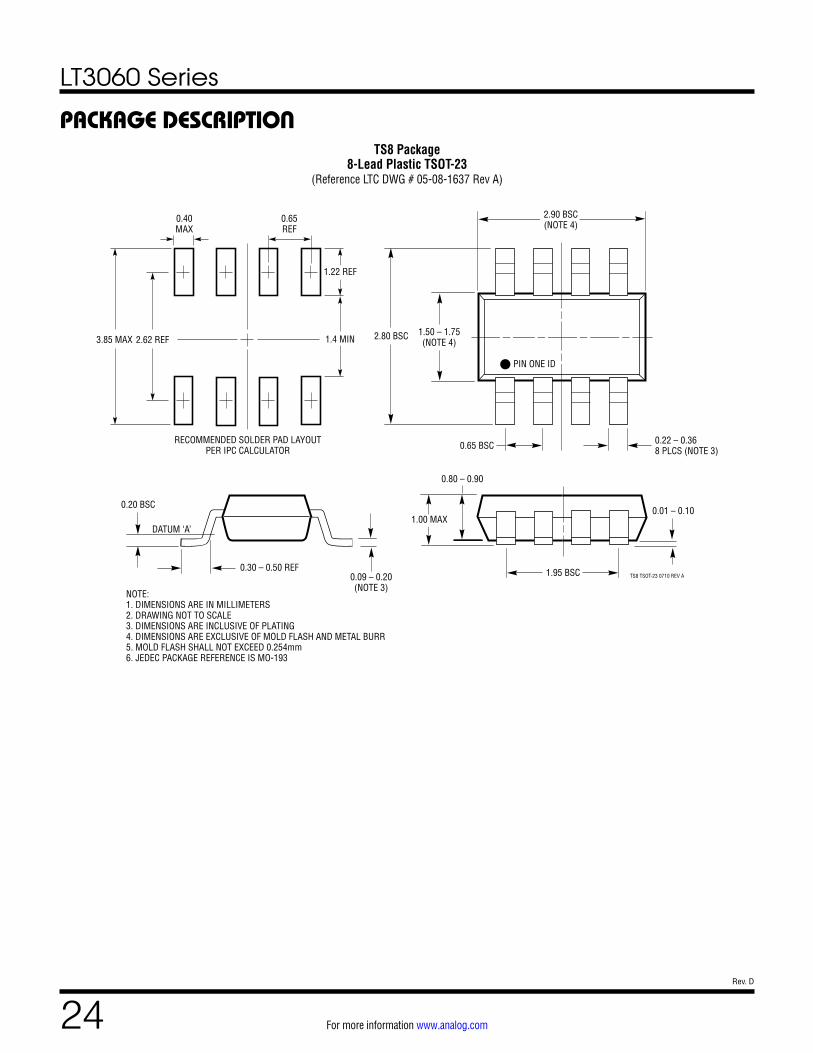
TS8 TSOT-23 0710 REV A
2.90 BSC(NOTE 4)
0.65 BSC
1.95 BSC
0.80 – 0.90
1.00 MAX0.01 – 0.10
0.20 BSC
0.30 – 0.50 REF
PIN ONE ID
NOTE:1. DIMENSIONS ARE IN MILLIMETERS2. DRAWING NOT TO SCALE3. DIMENSIONS ARE INCLUSIVE OF PLATING4. DIMENSIONS ARE EXCLUSIVE OF MOLD FLASH AND METAL BURR5. MOLD FLASH SHALL NOT EXCEED 0.254mm6. JEDEC PACKAGE REFERENCE IS MO-193
3.85 MAX
0.40MAX
0.65REF
RECOMMENDED SOLDER PAD LAYOUTPER IPC CALCULATOR
1.4 MIN2.62 REF
1.22 REF
TS8 Package8-Lead Plastic TSOT-23
(Reference LTC DWG # 05-08-1637 Rev A)
PACKAGE DESCRIPTION

LT3060 Series
25Rev. D
For more information www.analog.com
Information furnished by Analog Devices is believed to be accurate and reliable. However, no responsibility is assumed by Analog Devices for its use, nor for any infringements of patents or other rights of third parties that may result from its use. Specifications subject to change without notice. No license is granted by implication or otherwise under any patent or patent rights of Analog Devices.
REVISION HISTORYREV DATE DESCRIPTION PAGE NUMBER
A 7/10 Added fixed voltage options for 1.2V, 1.5V, 1.8V, 2.5V, 3.3V and 5V 1-26
B 5/11 Extended MP-Grade to 150°CUpdated test conditions for ADJ Pin Bias Current and Reverse Output Current in Applications Information section
2-719-20
C 9/14 Added fixed voltage options for 15VUpdated available packaging in Related Parts section
1 to 14, 17, 2126
D 05/21 Added AEC-Q100 Qualified for Automotive Applications to Features tableReplaced Lead Free Finish with Tape And Reel (Mini)Replaced suffix PBF with TRMPBFAdded “AUTOMOTIVE PRODUCTS**” Table + Supplemental Text”
12, 32, 3
3

LT3060 Series
26Rev. D
For more information www.analog.com ANALOG DEVICES, INC. 2010–2021www.analog.com
05/21
RELATED PARTSPART NUMBER DESCRIPTION COMMENTS
LT1761 100mA, Low Noise LDO 300mV Dropout Voltage, Low Noise: 20µVRMS, VIN = 1.8V to 20V, ThinSOT Package
LT1762 150mA, Low Noise LDO 300mV Dropout Voltage, Low Noise: 20µVRMS, VIN = 1.8V to 20V, MS8 Package
LT1763 500mA, Low Noise LDO 300mV Dropout Voltage, Low Noise: 20µVRMS, VIN = 1.8V to 20V, SO8 and 4mm × 3mm DFN Packages
LT1764/ LT1764A
3A, Fast Transient Response, Low Noise LDO
340mV Dropout Voltage, Low Noise: 40µVRMS, VIN = 2.7V to 20V, TO-220 and DD Packages, LT1764A Version Stable Also with Ceramic Capacitors
LT1962 300mA, Low Noise LDO 270mV Dropout Voltage, Low Noise: 20µVRMS, VIN = 1.8V to 20V, MS8 Package
LT1963/ LT1963A
1.5A Low Noise, Fast Transient Response LDO
340mV Dropout Voltage, Low Noise: 40µVRMS, VIN = 2.5V to 20V, LT1963A Version Stable with Ceramic Capacitors; TO-220, DD, SOT-223 and SO8 Packages
LT1964 200mA, Low Noise, Negative LDO 340mV Dropout Voltage, Low Noise 30µVRMS, VIN = –1.8V to –20V, ThinSOT and 3mm × 3mm DFN Packages
LT1965 1.1A, Low Noise, Low Dropout Linear Regulator
290mV Dropout Voltage, Low Noise: 40µVRMS, VIN: 1.8V to 20V, VOUT: 1.2V to 19.5V, Stable with Ceramic Capacitors; TO-220, DD-Pak, MSOP and 3mm × 3mm DFN Packages
LT3008 20mA, 45V, 3µA IQ Micropower LDO 300mV Dropout Voltage, Low IQ: 3µA, VIN = 2V to 45V, VOUT = 0.6V to 39.5V; ThinSOT and 2mm × 2mm DFN-6 Packages
LT3009 20mA, 3µA IQ Micropower LDO 280mV Dropout Voltage, Low IQ: 3µA, VIN = 1.6V to 20V, 2mm × 2mm DFN and SC70 Packages
LT3050 100mA, Low Noise Linear Regulator with Precision Current Limit and Diagnostic Functions.
340mV Dropout Voltage, Low Noise: 30µVRMS, VIN: 1.6V to 45V, VOUT: 0.6V to 44.5V, Programmable Precision Current Limit: ±5%, Programmable Minimum IOUT Monitor, Output Current Monitor, Fault Indicator, Reverse Protection; 12-Lead 2mm × 3mm DFN and MSOP Packages.
LT3080/ LT3080-1
1.1A, Parallelable, Low Noise, Low Dropout Linear Regulator
300mV Dropout Voltage (2-Supply Operation), Low Noise: 40µVRMS, VIN: 1.2V to 36V, VOUT: 0V to 35.7V, Current-Based Reference with 1-Resistor VOUT Set; Directly Parallelable (No Op Amp Required), Stable with Ceramic Capacitors; TO-220, SOT-223, MSOP and 3mm × 3mm DFN Packages; LT3080-1 Version Has Integrated Internal Ballast Resistor
LT3082 200mA, Parallelable, Single Resistor, Low Dropout Linear Regulator
Outputs May Be Paralleled for Higher Output, Current or Heat Spreading, Wide Input Voltage Range: 1.2V to 40V Low Value Input/Output Capacitors Required: 0.22μF, Single Resistor Sets Output Voltage, Initial Set Pin Current Accuracy: 1%, Low Output Noise: 40μVRMS (10Hz to 100kHz) Reverse-Battery Protection, Reverse-Current Protection; 8-Lead SOT-23, 3-Lead SOT-223 and 8-Lead 3mm × 3mm DFN Packages
LT3085 500mA, Parallelable, Low Noise, Low Dropout Linear Regulator
275mV Dropout Voltage (2-Supply Operation), Low Noise: 40µVRMS, VIN: 1.2V to 36V, VOUT: 0V to 35.7V, Current-Based Reference with 1-Resistor VOUT Set, Directly Parallelable (No Op Amp Required), Stable with Ceramic Capacitors; MS8E and 2mm × 3mm DFN-6 Packages
LT3092 200mA 2-Terminal Programmable Current Source
Programmable 2-Terminal Current Source, Maximum Output Current: 200mA, Wide Input Voltage Range: 1.2V to 40V, Resistor Ratio Sets Output Current, Initial Set Pin Current Accuracy: 1%, Current Limit and Thermal Shutdown Protection, Reverse-Voltage Protection, Reverse-Current Protection; 8-Lead SOT-23, 3-Lead SOT-223 and 8-Lead 3mm × 3mm DFN Packages
12V Low Noise Regulator
TYPICAL APPLICATION
3060 TA04
IN
SHDN
OUT
ADJ
GND REF/BYP
LT3060VIN13V TO45V
VOUT12V AT 100mA30µVRMS NOISE
1µF 10µFCFF10nF
2.37M1%
10nF
124k1%
0 0.1 0.2 0.7 0.8 0.9 1.00.3 0.4 0.5 0.6TIME (ms)
OUTP
UT V
OLTA
GE D
EVIA
TION
50m
V/DI
V
LOADCURRENT
100mA/DIV
3060 TA04b
VIN = 13V
CFF = 0
CFF = 10nF
∆IL = 10mA TO 100mA