Adc
85
SALEM COLLEGE OF ENGINEERING AND TECHNOLOGY SALEM -636111 Department of ECE Analog and Digital Circuits Laboratory PREPARED BY G. MOHANAVEL ASSISTANT PROFESSOR DEPARTMENT OF ECE
-
Upload
kvinothscet -
Category
Documents
-
view
5 -
download
0
description
adc
Transcript of Adc

SALEM COLLEGE
OF ENGINEERING AND TECHNOLOGY
SALEM -636111
Department of ECE
Analog and Digital Circuits Laboratory
PREPARED BY
G. MOHANAVEL
ASSISTANT PROFESSOR
DEPARTMENT OF ECE

Page | 2
EC6311 ANALOG AND DIGITAL CIRCUITS LABORATORY
LIST OF EXPERIMENTS
LIST OF ANALOG EXPERIMENTS
1. Half wave, Full wave rectifiers, filters, Power supplies.
2. Frequency response of CE, CB, CC and CS Amplifiers.
3. Darlington Amplifiers.
4. Differential Amplifiers – Transfer Characteristics, CMRR Measurement.
5. Cascode / Cascade Amplifiers.
6. Class A and Class B Power Amplifiers.
7. Determination of Bandwidth of Single stage and Multi stage Amplifiers.
8. Spice Simulation of Common Emitter and Common Source Amplifiers.
LIST OF DIGITAL EXPERIMENTS
9. Design and Implementation of Code Converters using Logic Gates
(i). BCD to Excess – 3 Code and Vice versa. (ii). Binary to Gray code and vice
versa.
10. Design and implementation of 4-bit binary Adder/Subtractor and BCD adder
using IC 7483.
11. Design and implementation of Multiplexers and Demultiplexers using logic gates.
12. Design and implementation of Encoders and Decoders using logic Gates.
13. Construction and verification of 4 bit ripple counter and Mod 10 and Mod 12
Ripple counters.
14. Design and implementation of Synchronous Up/Down counters.
15. Implementation of SISO, SIPO, PISO, PIPO Shift Registers using Flip Flops.
Page | 3
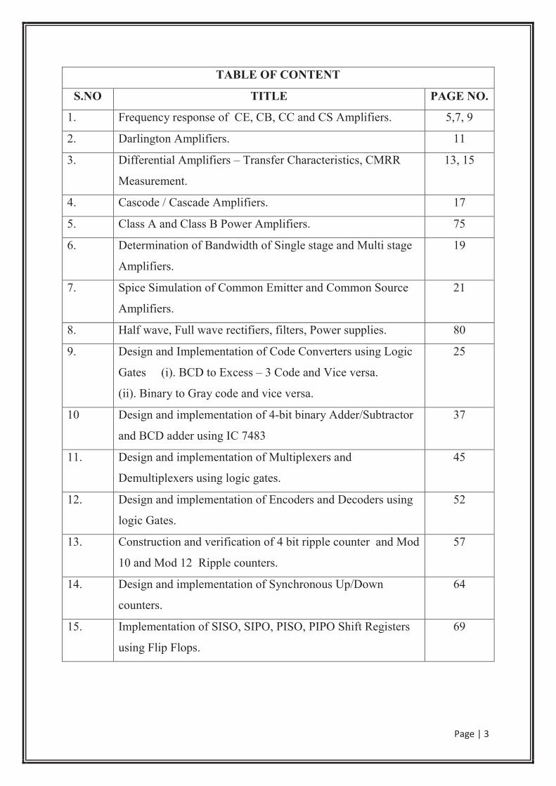
TABLE OF CONTENT
S.NO TITLE PAGE NO.
1. Frequency response of CE, CB, CC and CS Amplifiers. 5,7, 9
2. Darlington Amplifiers. 11
3. Differential Amplifiers – Transfer Characteristics, CMRR
Measurement.
13, 15
4. Cascode / Cascade Amplifiers. 17
5. Class A and Class B Power Amplifiers. 75
6. Determination of Bandwidth of Single stage and Multi stage
Amplifiers.
19
7. Spice Simulation of Common Emitter and Common Source
Amplifiers.
21
8. Half wave, Full wave rectifiers, filters, Power supplies. 80
9. Design and Implementation of Code Converters using Logic
Gates (i). BCD to Excess – 3 Code and Vice versa.
(ii). Binary to Gray code and vice versa.
25
10 Design and implementation of 4-bit binary Adder/Subtractor
and BCD adder using IC 7483
37
11. Design and implementation of Multiplexers and
Demultiplexers using logic gates.
45
12. Design and implementation of Encoders and Decoders using
logic Gates.
52
13. Construction and verification of 4 bit ripple counter and Mod
10 and Mod 12 Ripple counters.
57
14. Design and implementation of Synchronous Up/Down
counters.
64
15. Implementation of SISO, SIPO, PISO, PIPO Shift Registers
using Flip Flops.
69

Page | 75
CLASS – A POWER AMPLIFIER

Page | 76
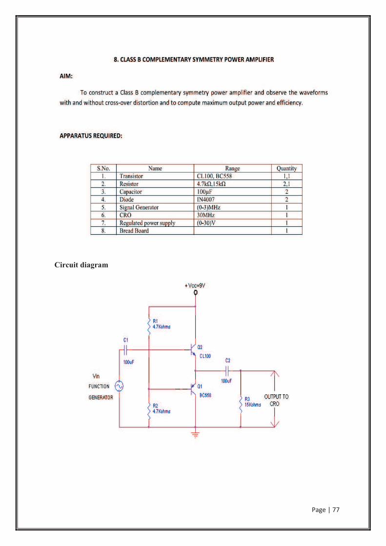
Page | 77
Circuit diagram

Page | 78
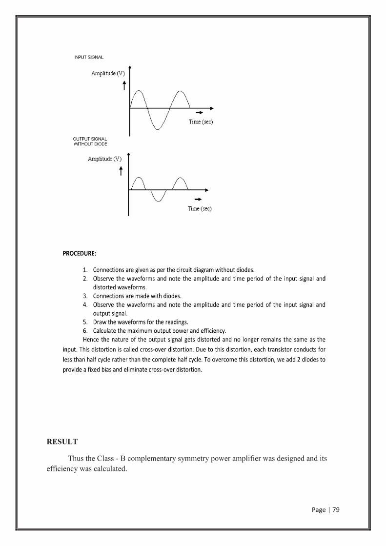
Class – B Complementary Symmetry Amplifier with Diodes
Page | 79
RESULT
Thus the Class - B complementary symmetry power amplifier was designed and its
efficiency was calculated.
Page | 80
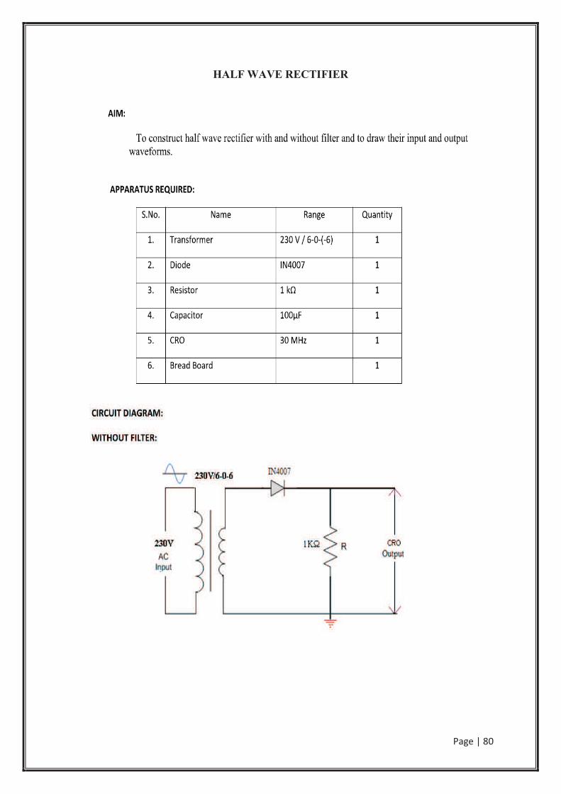
HALF WAVE RECTIFIER

Page | 81

Page | 82

Page | 83
FULL WAVE RECTIFIER

Page | 84
FULL WAVE RECTIFIER WITH FILTER

Page | 85
PROCEDURE
RESULT
Thus the full wave rectifier with and without filter were designed and its waveform were
drawn.

ANALOG AND DIGITAL CIRCUITS LAB MANUAL/ III rd SEM/ ECE Page 25
9. DESIGN AND IMPLEMENTATION OF CODE CONVERTOR
Aim:
To design and implement 4-bit
(i) Binary to gray code converter
(ii) Gray to binary code converter
(iii) BCD to excess-3 code converter
(iv) Excess-3 to BCD code converter
APPARATUS REQUIRED:
Sl.No. Component Specification Qty.
1. X-OR GATE IC 7486 1
2. AND GATE IC 7408 1
3. OR GATE IC 7432 1
4. NOT GATE IC 7404 1
5. IC TRAINER KIT - 1
6. PATCH CORDS - 35
THEORY:
The availability of large variety of codes for the same discrete elements of information
results in the use of different codes by different systems. A conversion circuit must be inserted
between the two systems if each uses different codes for same information. Thus, code converter
is a circuit that makes the two systems compatible even though each uses different binary code.
The bit combination assigned to binary code to gray code. Since each code uses four bits
to represent a decimal digit. There are four inputs and four outputs. Gray code is a non-weighted
code.

ANALOG AND DIGITAL CIRCUITS LAB MANUAL/ III rd SEM/ ECE Page 26
The input variable are designated as B3, B2, B1, B0 and the output variables are
designated as C3, C2, C1, Co. from the truth table, combinational circuit is designed. The
Boolean functions are obtained from K-Map for each output variable.
A code converter is a circuit that makes the two systems compatible even though each
uses a different binary code. To convert from binary code to Excess-3 code, the input lines must
supply the bit combination of elements as specified by code and the output lines generate the
corresponding bit combination of code. Each one of the four maps represents one of the four
outputs of the circuit as a function of the four input variables.
A two-level logic diagram may be obtained directly from the Boolean expressions
derived by the maps. These are various other possibilities for a logic diagram that implements
this circuit. Now the OR gate whose output is C+D has been used to implement partially each of
three outputs.
Logic Diagram:
BINARY TO GRAY CODE CONVERTOR
ANALOG AND DIGITAL CIRCUITS LAB MANUAL/ III rd SEM/ ECE Page 27
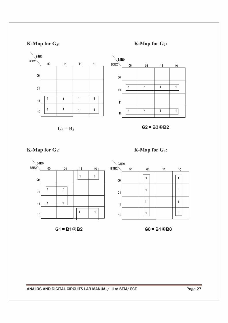
K-Map for G3: K-Map for G2:
G3 = B3
K-Map for G1: K-Map for G0:
ANALOG AND DIGITAL CIRCUITS LAB MANUAL/ III rd SEM/ ECE Page 28
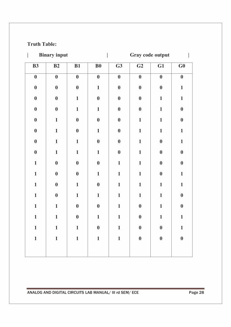
Truth Table:
| Binary input | Gray code output |
B3 B2 B1 B0 G3 G2 G1 G0
0
0
0
0
0
0
0
0
1
1
1
1
1
1
1
1
0
0
0
0
1
1
1
1
0
0
0
0
1
1
1
1
0
0
1
1
0
0
1
1
0
0
1
1
0
0
1
1
0
1
0
1
0
1
0
1
0
1
0
1
0
1
0
1
0
0
0
0
0
0
0
0
1
1
1
1
1
1
1
1
0
0
0
0
1
1
1
1
1
1
1
1
0
0
0
0
0
0
1
1
1
1
0
0
0
0
1
1
1
1
0
0
0
1
1
0
0
1
1
0
0
1
1
0
0
1
1
0

ANALOG AND DIGITAL CIRCUITS LAB MANUAL/ III rd SEM/ ECE Page 29
Logic Diagram:
GRAY CODE TO BINARY CONVERTOR
K-Map for B3: K-Map for B2:
B3 = G3

ANALOG AND DIGITAL CIRCUITS LAB MANUAL/ III rd SEM/ ECE Page 30
K-Map for B1: K-Map for B0:
Truth Table:
| Gray Code | Binary Code |
G3 G2 G1 G0 B3 B2 B1 B0
0
0
0
0
0
0
0
0
0
0
0
0
1
1
1
1
0
0
1
1
1
1
0
0
0
1
1
0
0
1
1
0
0
0
0
0
0
0
0
0
0
0
0
0
1
1
1
1
0
0
1
1
0
0
1
1
0
1
0
1
0
1
0
1

ANALOG AND DIGITAL CIRCUITS LAB MANUAL/ III rd SEM/ ECE Page 31
1
1
1
1
1
1
1
1
1
1
1
1
0
0
0
0
0
0
1
1
1
1
0
0
0
1
1
0
0
1
1
0
1
1
1
1
1
1
1
1
0
0
0
0
1
1
1
1
0
0
1
1
0
0
1
1
0
1
0
1
0
1
0
1
Logic Diagram:
BCD TO EXCESS-3 CONVERTOR
ANALOG AND DIGITAL CIRCUITS LAB MANUAL/ III rd SEM/ ECE Page 32
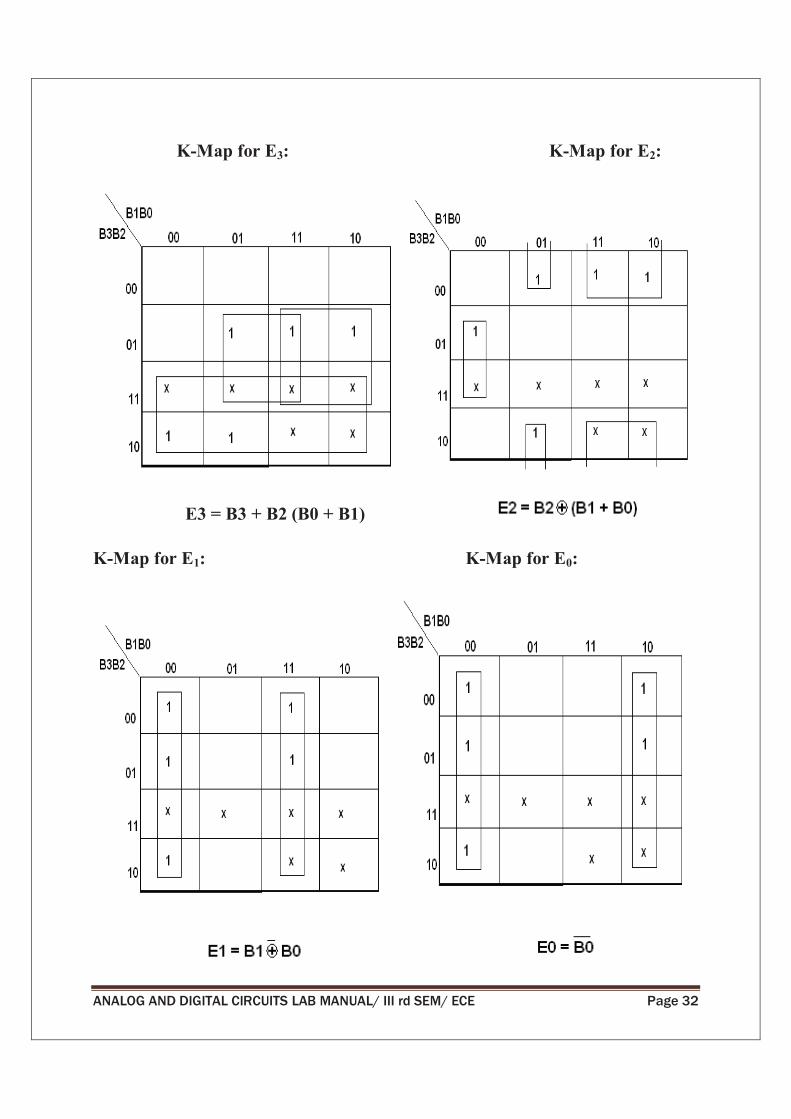
K-Map for E3: K-Map for E2:
E3 = B3 + B2 (B0 + B1)
K-Map for E1: K-Map for E0:

ANALOG AND DIGITAL CIRCUITS LAB MANUAL/ III rd SEM/ ECE Page 33
Truth Table:
| BCD input | Excess 3 output |
B3 B2 B1 B0 G3 G2 G1 G0
0
0
0
0
0
0
0
0
1
1
1
1
1
1
1
1
0
0
0
0
1
1
1
1
0
0
0
0
1
1
1
1
0
0
1
1
0
0
1
1
0
0
1
1
0
0
1
1
0
1
0
1
0
1
0
1
0
1
0
1
0
1
0
1
0
0
0
0
0
1
1
1
1
1
x
x
x
x
x
x
0
1
1
1
1
0
0
0
0
1
x
x
x
x
x
x
1
0
0
1
1
0
0
1
1
0
x
x
x
x
x
x
1
0
1
0
1
0
1
0
1
0
x
x
x
x
x
x

ANALOG AND DIGITAL CIRCUITS LAB MANUAL/ III rd SEM/ ECE Page 34
Logic Diagram:
EXCESS-3 TO BCD CONVERTOR
K-Map for A: K-Map for B:
A = X1 X2 + X3 X4 X1

ANALOG AND DIGITAL CIRCUITS LAB MANUAL/ III rd SEM/ ECE Page 35
K-Map for C: K-Map for D:
Truth Table:
| Excess 3 Input | BCD Output |
B3 B2 B1 B0 G3 G2 G1 G0
0
0
0
0
0
1
1
0
1
1
1
1
0
0
1
0
0
1
1
0
0
1
0
1
0
1
0
1
0
0
0
0
0
0
0
0
0
0
0
1
1
1
0
0
1
1
0
0
1
0
1
0
1
0
1
0

ANALOG AND DIGITAL CIRCUITS LAB MANUAL/ III rd SEM/ ECE Page 36
1
1
1
0
0
1
1
1
0
0
1
0
0
1
1
1
0
0
1
0
0
1
0
1
PROCEDURE:
(i) Connections were given as per circuit diagram.
(ii) Logical inputs were given as per truth table
(iii) Observe the logical output and verify with the truth tables.
Result:
Thus, binary to gray code converter, Gray to binary code converter, BCD to excess-3
code converter, Excess-3 to BCD code converter was implemented.
ANALOG AND DIGITAL CIRCUITS LAB MANUAL/ III rd SEM/ ECE Page 37
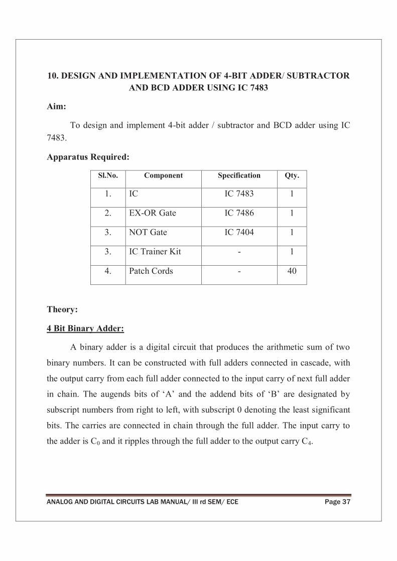
10. DESIGN AND IMPLEMENTATION OF 4-BIT ADDER/ SUBTRACTOR
AND BCD ADDER USING IC 7483
Aim:
To design and implement 4-bit adder / subtractor and BCD adder using IC
7483.
Apparatus Required:
Sl.No. Component Specification Qty.
1. IC IC 7483 1
2. EX-OR Gate IC 7486 1
3. NOT Gate IC 7404 1
3. IC Trainer Kit - 1
4. Patch Cords - 40
Theory:
4 Bit Binary Adder:
A binary adder is a digital circuit that produces the arithmetic sum of two
binary numbers. It can be constructed with full adders connected in cascade, with
the output carry from each full adder connected to the input carry of next full adder
subscript numbers from right to left, with subscript 0 denoting the least significant
bits. The carries are connected in chain through the full adder. The input carry to
the adder is C0 and it ripples through the full adder to the output carry C4.

ANALOG AND DIGITAL CIRCUITS LAB MANUAL/ III rd SEM/ ECE Page 38
4 Bit Binary Subtractor:
The circuit for subtracting A-B consists of an adder with inverters, placed
carry C0 must be equal to 1 when performing subtraction.
4 Bit Binary Adder/Subtractor:
The addition and subtraction operation can be combined into one circuit with
one common binary adder. The mode input M controls the operation. When M=0,
the circuit is adder circuit. When M=1, it becomes subtractor.
4 Bit BCD Adder:
Consider the arithmetic addition of two decimal digits in BCD, together with
an input carry from a previous stage. Since each input digit does not exceed 9, the
output sum cannot be greater than 19, the 1 in the sum being an input carry. The
output of two decimal digits must be represented in BCD and should appear in the
form listed in the columns.
ABCD adder that adds 2 BCD digits and produce a sum digit in BCD. The 2
decimal digits, together with the input carry, are first added in the top 4 bit adder to
produce the binary sum.

ANALOG AND DIGITAL CIRCUITS LAB MANUAL/ III rd SEM/ ECE Page 39
Pin Diagram for IC 7483:
Logic Diagram:
4-Bit Binary Adder

ANALOG AND DIGITAL CIRCUITS LAB MANUAL/ III rd SEM/ ECE Page 40
4-Bit Binary Subtractor
4-Bit Binary Adder/Subtractor

ANALOG AND DIGITAL CIRCUITS LAB MANUAL/ III rd SEM/ ECE Page 41
Truth Table:
Input Data A Input Data B Addition Subtraction
A4 A3 A2 A1 B4 B3 B2 B1 C S4 S3 S2 S1 B D4 D3 D2 D1
1 0 0 0 0 0 1 0 0 1 0 1 0 1 0 1 1 0
1 0 0 0 1 0 0 0 1 0 0 0 0 1 0 0 0 0
0 0 1 0 1 0 0 0 0 1 0 1 0 0 1 0 1 0
0 0 0 1 0 1 1 1 0 1 0 0 0 0 1 0 1 0
1 0 1 0 1 0 1 1 1 0 0 1 0 0 1 1 1 1
1 1 1 0 1 1 1 1 1 1 0 1 0 0 1 1 1 1
1 0 1 0 1 1 0 1 1 0 1 1 1 0 1 1 0 1

ANALOG AND DIGITAL CIRCUITS LAB MANUAL/ III rd SEM/ ECE Page 42
BCD ADDER
K- MAP
Y = S4 (S3 + S2)

ANALOG AND DIGITAL CIRCUITS LAB MANUAL/ III rd SEM/ ECE Page 43
Truth Table:
BCD SUM CARRY
S4 S3 S2 S1 C
0 0 0 0 0
0 0 0 1 0
0 0 1 0 0
0 0 1 1 0
0 1 0 0 0
0 1 0 1 0
0 1 1 0 0
0 1 1 1 0
1 0 0 0 0
1 0 0 1 0
1 0 1 0 1
1 0 1 1 1
1 1 0 0 1
1 1 0 1 1
1 1 1 0 1
1 1 1 1 1

ANALOG AND DIGITAL CIRCUITS LAB MANUAL/ III rd SEM/ ECE Page 44
PROCEDURE:
(i) Connections were given as per circuit diagram.
(ii) Logical inputs were given as per truth table
(iii) Observe the logical output and verify with the truth tables.
Result:
Thus, the 4-bit adder / subtractor and BCD adder using IC 7483 was
designed and implement.

ANALOG AND DIGITAL CIRCUITS LAB MANUAL/ III rd SEM/ ECE Page 45
11. DESIGN AND IMPLEMENTATION OF MULTIPLEXER AND
DEMULTIPLEXER
Aim:
To design and implement multiplexer and De-multiplexer using logic gates and study of
IC 74150 and IC 74154.
Apparatus Required:
Sl.No. Component Specification Qty.
1. 3 I/P AND GATE IC 7411 2
2. OR GATE IC 7432 1
3. NOT GATE IC 7404 1
2. IC TRAINER KIT - 1
3. PATCH CORDS - 32
Theory:
MULTIPLEXER:
Multiplexer means transmitting a large number of information units over a smaller
number of channels or lines. A digital multiplexer is a combinational circuit that selects binary
information from one of many input lines and directs it to a single output line. The selection of a
particular input line is controlled by a set of selection lines. Normally there are 2n input line and
n selection lines whose bit combination determine which input is selected.
DEMULTIPLEXER:
The function of Demultiplexer is in contrast to multiplexer function. It takes information
from one line and distributes it to a given number of output lines. For this reason, the
demultiplexer is also known as a data distributor. Decoder can also be used as demultiplexer.

ANALOG AND DIGITAL CIRCUITS LAB MANUAL/ III rd SEM/ ECE Page 46
In the 1: 4 demultiplexer circuit, the data input line goes to all of the AND gates. The data
select lines enable only one gate at a time and the data on the data input line will pass through the
selected gate to the associated data output line.
Block Diagram for 4:1 Multiplexer:
Function Table:
S1 S0 INPUTS Y
0 0 D0
0 1
1 0
1 1
ANALOG AND DIGITAL CIRCUITS LAB MANUAL/ III rd SEM/ ECE Page 47
Circuit Diagram For Multiplexer:
Truth Table:
S1 S0 Y = OUTPUT
0 0 D0
0 1 D1
1 0 D2
1 1 D3

ANALOG AND DIGITAL CIRCUITS LAB MANUAL/ III rd SEM/ ECE Page 48
Block Diagram for 1:4 Demultiplexer:
Function Table
S1 S0 INPUT
0 0
0 1
1 0
1 1
ANALOG AND DIGITAL CIRCUITS LAB MANUAL/ III rd SEM/ ECE Page 49
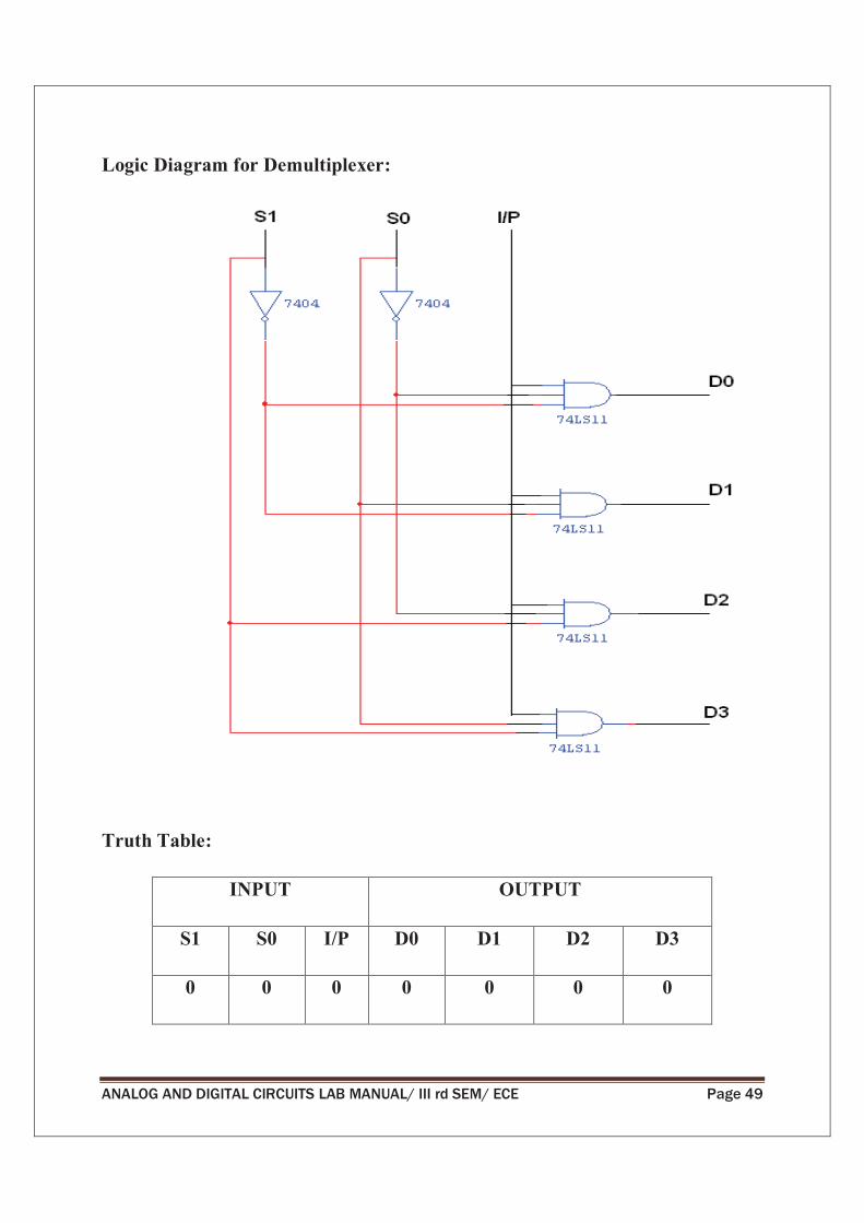
Logic Diagram for Demultiplexer:
Truth Table:
INPUT OUTPUT
S1 S0 I/P D0 D1 D2 D3
0 0 0 0 0 0 0

ANALOG AND DIGITAL CIRCUITS LAB MANUAL/ III rd SEM/ ECE Page 50
0 0 1 1 0 0 0
0 1 0 0 0 0 0
0 1 1 0 1 0 0
1 0 0 0 0 0 0
1 0 1 0 0 1 0
1 1 0 0 0 0 0
1 1 1 0 0 0 1
Pin Diagram for IC 74150:
ANALOG AND DIGITAL CIRCUITS LAB MANUAL/ III rd SEM/ ECE Page 51
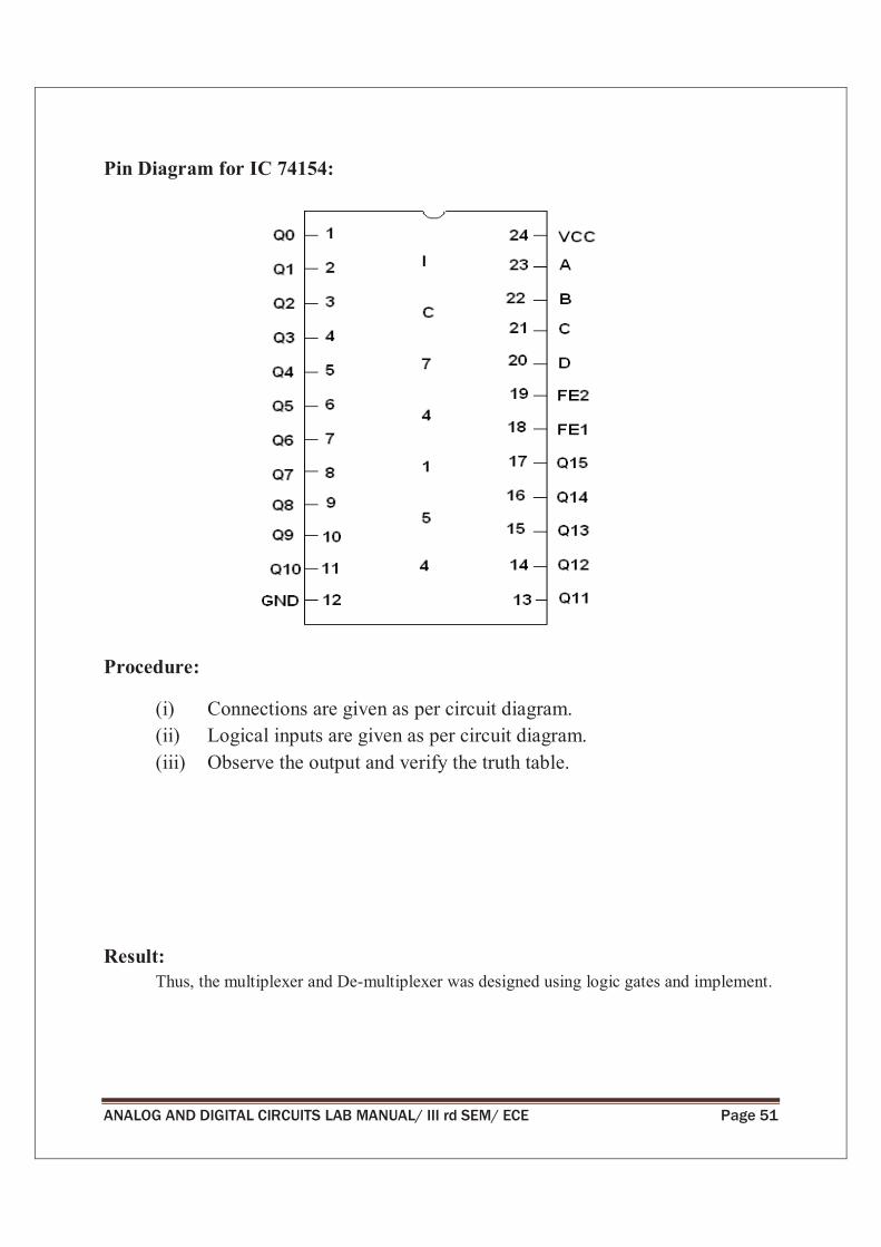
Pin Diagram for IC 74154:
Procedure:
(i) Connections are given as per circuit diagram.
(ii) Logical inputs are given as per circuit diagram.
(iii) Observe the output and verify the truth table.
Result:
Thus, the multiplexer and De-multiplexer was designed using logic gates and implement.

ANALOG AND DIGITAL CIRCUITS LAB MANUAL/ III rd SEM/ ECE Page 52
12. DESIGN AND IMPLEMENTATION OF ENCODER AND DECODER
Aim:
To design and implement encoder and decoder using logic gates and study of IC 7445
and IC 74147.
Apparatus Required:
Sl.No. Component Specification Qty.
1. 3 I/P NAND Gate IC 7410 2
2. OR Gate IC 7432 3
3. NOT Gate IC 7404 1
2. IC Trainer Kit - 1
3. Patch Cords - 27
Theory:
Encoder:
An encoder is a digital circuit that perform inverse operation of a decoder.
An encoder has 2n input lines and n output lines. In encoder the output lines
generates the binary code corresponding to the input value. In octal to binary
encoder it has eight inputs, one for each octal digit and three output that generate
the corresponding binary code. In encoder it is assumed that only one input has a
value of one at any given time otherwise the circuit is meaningless. It has an
ambiguila that when all inputs are zero the outputs are zero. The zero outputs can
also be generated when D0 = 1.
ANALOG AND DIGITAL CIRCUITS LAB MANUAL/ III rd SEM/ ECE Page 53
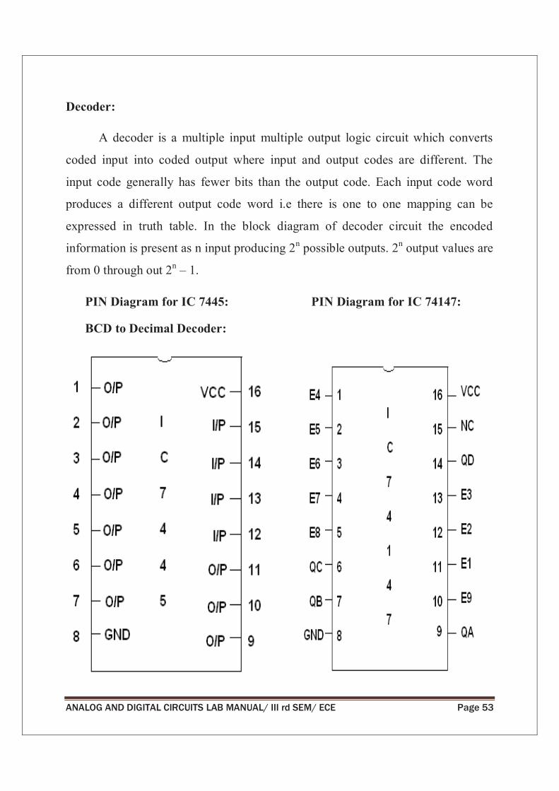
Decoder:
A decoder is a multiple input multiple output logic circuit which converts
coded input into coded output where input and output codes are different. The
input code generally has fewer bits than the output code. Each input code word
produces a different output code word i.e there is one to one mapping can be
expressed in truth table. In the block diagram of decoder circuit the encoded
information is present as n input producing 2n possible outputs. 2
n output values are
from 0 through out 2n
1.
PIN Diagram for IC 7445: PIN Diagram for IC 74147:
BCD to Decimal Decoder:

ANALOG AND DIGITAL CIRCUITS LAB MANUAL/ III rd SEM/ ECE Page 54
Logic Diagram for Encoder:
Truth Table:
INPUT OUTPUT
Y1 Y2 Y3 Y4 Y5 Y6 Y7 A B C
1 0 0 0 0 0 0 0 0 1
0 1 0 0 0 0 0 0 1 0

ANALOG AND DIGITAL CIRCUITS LAB MANUAL/ III rd SEM/ ECE Page 55
0 0 1 0 0 0 0 0 1 1
0 0 0 1 0 0 0 1 0 0
0 0 0 0 1 0 0 1 0 1
0 0 0 0 0 1 0 1 1 0
0 0 0 0 0 0 1 1 1 1
Logic Diagram for Decoder:

ANALOG AND DIGITAL CIRCUITS LAB MANUAL/ III rd SEM/ ECE Page 56
Truth Table:
INPUT OUTPUT
E A B D0 D1 D2 D3
1 0 0 1 1 1 1
0 0 0 0 1 1 1
0 0 1 1 0 1 1
0 1 0 1 1 0 1
0 1 1 1 1 1 0
Procedure:
(i) Connections are given as per circuit diagram.
(ii) Logical inputs are given as per circuit diagram.
(iii) Observe the output and verify the truth table.
Result:
Thus, the encoder and decoder were designed using logic gates and implement.

ANALOG AND DIGITAL CIRCUITS LAB MANUAL/ III rd SEM/ ECE Page 57
13. CONSTRUCTION AND VERIFICATION OF 4 BIT RIPPLE COUNTER
AND MOD 10/MOD 12 RIPPLE COUNTER
Aim:
To design and verify 4 bit ripple counter mod 10/ mod 12 ripple counter.
Apparatus Required:
Sl.No. Component Specification Qty.
1. JK FLIP FLOP IC 7476 2
2. NAND GATE IC 7400 1
3. IC TRAINER KIT - 1
4. PATCH CORDS - 30
Theory:
A counter is a register capable of counting number of clock pulse arriving at
its clock input. Counter represents the number of clock pulses arrived. A specified
sequence of states appears as counter output. This is the main difference between a
register and a counter. There are two types of counter, synchronous and
asynchronous. In synchronous common clock is given to all flip flop and in
asynchronous first flip flop is clocked by external pulse and then each successive
flip flop is clocked by Q or Q output of previous stage. A soon the clock of second
stage is triggered by output of first stage. Because of inherent propagation delay
time all flip flops are not activated at same time which results in asynchronous
operation.

ANALOG AND DIGITAL CIRCUITS LAB MANUAL/ III rd SEM/ ECE Page 58
PIN Diagram for IC 7476:
Logic Diagram for 4 Bit Ripple Counter:

ANALOG AND DIGITAL CIRCUITS LAB MANUAL/ III rd SEM/ ECE Page 59
Truth Table:
CLK QA QB QC QD
0 0 0 0 0
1 1 0 0 0
2 0 1 0 0
3 1 1 0 0
4 0 0 1 0
5 1 0 1 0
6 0 1 1 0
7 1 1 1 0
8 0 0 0 1
9 1 0 0 1
10 0 1 0 1
11 1 1 0 1
12 0 0 1 1
13 1 0 1 1
14 0 1 1 1
15 1 1 1 1

ANALOG AND DIGITAL CIRCUITS LAB MANUAL/ III rd SEM/ ECE Page 60
Logic Diagram for Mod - 10 Ripple Counter:
Truth Table:
CLK QA QB QC QD
0 0 0 0 0
1 1 0 0 0
2 0 1 0 0
3 1 1 0 0
4 0 0 1 0
5 1 0 1 0

ANALOG AND DIGITAL CIRCUITS LAB MANUAL/ III rd SEM/ ECE Page 61
6 0 1 1 0
7 1 1 1 0
8 0 0 0 1
9 1 0 0 1
10 0 0 0 0
Logic Diagram for Mod - 12 Ripple Counter:

ANALOG AND DIGITAL CIRCUITS LAB MANUAL/ III rd SEM/ ECE Page 62
Truth Table:
CLK QA QB QC QD
0 0 0 0 0
1 1 0 0 0
2 0 1 0 0
3 1 1 0 0
4 0 0 1 0
5 1 0 1 0
6 0 1 1 0
7 1 1 1 0
8 0 0 0 1
9 1 0 0 1
10 0 1 0 1
11 1 1 0 1
12 0 0 0 0

ANALOG AND DIGITAL CIRCUITS LAB MANUAL/ III rd SEM/ ECE Page 63
PROCEDURE:
(i) Connections are given as per circuit diagram.
(ii) Logical inputs are given as per circuit diagram.
(iii) Observe the output and verify the truth table.
Result:
Thus, the 4 bit ripple counter mod 10/ mod 12 ripple counters was designed and verified.
ANALOG AND DIGITAL CIRCUITS LAB MANUAL/ III rd SEM/ ECE Page 64
14. DESIGN AND IMPLEMENTATION OF 3 BIT SYNCHRONOUS
UP/DOWN COUNTER
Aim:
To design and implement 3 bit synchronous up/down counter.
Apparatus Required:
Sl.No. Component Specification Qty.
1. JK FLIP FLOP IC 7476 2
2. 3 I/P AND GATE IC 7411 1
3. OR GATE IC 7432 1
4. XOR GATE IC 7486 1
5. NOT GATE IC 7404 1
6. IC TRAINER KIT - 1
7. PATCH CORDS - 35
Theory:
A counter is a register capable of counting number of clock pulse arriving at
its clock input. Counter represents the number of clock pulses arrived. An up/down
counter is one that is capable of progressing in increasing order or decreasing order
through a certain sequence. An up/down counter is also called bidirectional
counter. Usually up/down operation of the counter is controlled by up/down signal.
When this signal is high counter goes through up sequence and when up/down
signal is low counter follows reverse sequence.

ANALOG AND DIGITAL CIRCUITS LAB MANUAL/ III rd SEM/ ECE Page 65
K- MAP
State Diagram:

ANALOG AND DIGITAL CIRCUITS LAB MANUAL/ III rd SEM/ ECE Page 66
Characteristics Table:
Q Qt+1 J K
0 0 0 X
0 1 1 X
1 0 X 1
1 1 X 0
Logic Diagram:

ANALOG AND DIGITAL CIRCUITS LAB MANUAL/ III rd SEM/ ECE Page 67
Truth Table:
Input
Up/Down
Present State
QA QB QC
Next State
QA+1 Q B+1 QC+1
A
JA KA
B
JB KB
C
JC KC
0 0 0 0 1 1 1 1 X 1 X 1 X
0 1 1 1 1 1 0 X 0 X 0 X 1
0 1 1 0 1 0 1 X 0 X 1 1 X
0 1 0 1 1 0 0 X 0 0 X X 1
0 1 0 0 0 1 1 X 1 1 X 1 X
0 0 1 1 0 1 0 0 X X 0 X 1
0 0 1 0 0 0 1 0 X X 1 1 X
0 0 0 1 0 0 0 0 X 0 X X 1
1 0 0 0 0 0 1 0 X 0 X 1 X
1 0 0 1 0 1 0 0 X 1 X X 1
1 0 1 0 0 1 1 0 X X 0 1 X
1 0 1 1 1 0 0 1 X X 1 X 1
1 1 0 0 1 0 1 X 0 0 X 1 X
1 1 0 1 1 1 0 X 0 1 X X 1
1 1 1 0 1 1 1 X 0 X 0 1 X
1 1 1 1 0 0 0 X 1 X 1 X 1

ANALOG AND DIGITAL CIRCUITS LAB MANUAL/ III rd SEM/ ECE Page 68
Procedure:
(i) Connections are given as per circuit diagram.
(ii) Logical inputs are given as per circuit diagram.
(iii) Observe the output and verify the truth table.
Result:
Thus, 3 bit synchronous up/down counter was designed and implemented.

ANALOG AND DIGITAL CIRCUITS LAB MANUAL/ III rd SEM/ ECE Page 69
15. DESIGN AND IMPLEMENTATION OF SHIFT REGISTER
Aim:
To design and implement
(i) Serial in serial out
(ii) Serial in parallel out
(iii) Parallel in serial out
(iv) Parallel in parallel out
Apparatus Required:
Sl.No. COMPONENT SPECIFICATION QTY.
1. D FLIP FLOP IC 7474 2
2. OR GATE IC 7432 1
3. IC TRAINER KIT - 1
4. PATCH CORDS - 35
Theory:
A register is capable of shifting its binary information in one or both
directions is known as shift register. The logical configuration of shift register
consist of a D-Flip flop cascaded with output of one flip flop connected to input of
next flip flop. All flip flops receive common clock pulses which causes the shift in
the output of the flip flop.The simplest possible shift register is one that uses only
flip flop. The output of a given flip flop is connected to the input of next flip flop
of the register. Each clock pulse shifts the content of register one bit position to
right.

ANALOG AND DIGITAL CIRCUITS LAB MANUAL/ III rd SEM/ ECE Page 70
Pin Diagram:
Logic Diagram:
SERIAL IN SERIAL OUT:

ANALOG AND DIGITAL CIRCUITS LAB MANUAL/ III rd SEM/ ECE Page 71
Truth Table:
CLK Serial in Serial out
1 1 0
2 0 0
3 0 0
4 1 1
5 X 0
6 X 0
7 X 1
Logic Diagram:
SERIAL IN PARALLEL OUT:

ANALOG AND DIGITAL CIRCUITS LAB MANUAL/ III rd SEM/ ECE Page 72
Truth Table:
CLK DATA
OUTPUT
QA QB QC QD
1 1 1 0 0 0
2 0 0 1 0 0
3 0 0 0 1 1
4 1 1 0 0 1
Logic Diagram:
PARALLEL IN SERIAL OUT:

ANALOG AND DIGITAL CIRCUITS LAB MANUAL/ III rd SEM/ ECE Page 73
Truth Table:
CLK Q3 Q2 Q1 Q0 O/P
0 1 0 0 1 1
1 0 0 0 0 0
2 0 0 0 0 0
3 0 0 0 0 1
Logic Diagram:
PARALLEL IN PARALLEL OUT:

ANALOG AND DIGITAL CIRCUITS LAB MANUAL/ III rd SEM/ ECE Page 74
Truth Table:
CLK
DATA INPUT OUTPUT
DA DB DC DD QA QB QC QD
1 1 0 0 1 1 0 0 1
2 1 0 1 0 1 0 1 0
Procedure:
(i) Connections are given as per circuit diagram.
(ii) Logical inputs are given as per circuit diagram.
(iii) Observe the output and verify the truth table.
Result:
Thus, the Serial in serial out, Serial in parallel out, Parallel in serial out,
Parallel in parallel out was designed and implemented using flip flops.

ANALOG AND DIGITAL CIRCUITS LAB MANUAL/ III rd SEM/ ECE Page 4
ANALOG EXPERIMENTS

ANALOG AND DIGITAL CIRCUITS LAB MANUAL/ III rd SEM/ ECE Page 5
1(a). COMMON EMITTER AMPLIFIER
Aim: To find the voltage gain of a CE amplifier and to find its frequency response
Apparatus:
S.No. Name Range Quantity
1. Transistor BC107 1
2. Resistor 1,1,1,1
3. Capacitor 10µf 3
4. Regulated power supply (0-30)V 1
5. Function Generator (0-3) MHz 1
6. CRO 30 MHz 1
7. Bread Board 1
Circuit Diagram:
Theory: The CE amplifier is a small signal amplifier. This small signal amplifier accepts low
voltage ac inputs and produces amplified outputs. A single stage BJT circuit may be employed as
a small signal amplifier; has two cascaded stages give much more amplification. Designing for a
particular voltage gain requires the use of a ac negative feedback to stabilize the gain. For good
bias stability, the emitter resistor voltage drop should be much larger than the base -emitter
voltage. And Re resistor will provide the required negative feedback to the circuit. CE is
provided to provide necessary gain to the circuit. All bypass capacitors should be selected to

ANALOG AND DIGITAL CIRCUITS LAB MANUAL/ III rd SEM/ ECE Page 6
have the smallest possible capacitance value, both to minimize the physical size of the circuit for
economy. The coupling capacitors should have a negligible effect on the frequency response of
the circuit.
Procedure: 1. Connect the circuit as per the circuit diagram.
2. Give l00Hz signal and 20mv p-p as Vs from the signal generator
3. Observe the output on CRO and note down the output voltage.
4. Keeping input voltage constant and by varying the frequency in steps 100Hz-1MHz, note
down the corresponding output voltages.
5. Calculate gain in dB and plot the frequency response on semi log sheet
Tabular Form:
Input voltage (Vi)=
FREQUENCY OUTPUT
VOLTAGE(Vo)
GAIN Av=Vo/Vi
GAIN IN dB
GAIN IN dB
20 log gain
Model Graph:
Result:
Thus, the voltage gain and frequency response of a CE amplifier was measured.
ANALOG AND DIGITAL CIRCUITS LAB MANUAL/ III rd SEM/ ECE Page 7
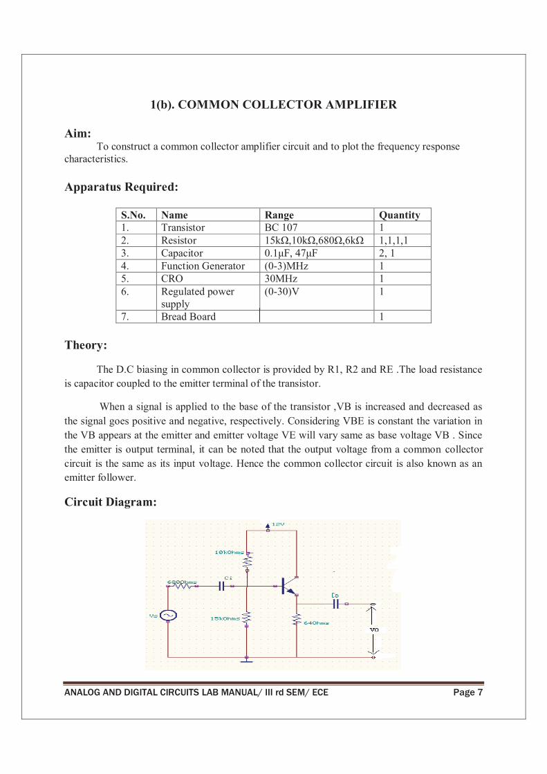
1(b). COMMON COLLECTOR AMPLIFIER
Aim: To construct a common collector amplifier circuit and to plot the frequency response
characteristics.
Apparatus Required:
S.No. Name Range Quantity
1. Transistor BC 107 1
2. Resistor 1,1,1,1
3. Capacitor 2, 1
4. Function Generator (0-3)MHz 1
5. CRO 30MHz 1
6. Regulated power
supply
(0-30)V 1
7. Bread Board 1
Theory:
The D.C biasing in common collector is provided by R1, R2 and RE .The load resistance
is capacitor coupled to the emitter terminal of the transistor.
When a signal is applied to the base of the transistor ,VB is increased and decreased as
the signal goes positive and negative, respectively. Considering VBE is constant the variation in
the VB appears at the emitter and emitter voltage VE will vary same as base voltage VB . Since
the emitter is output terminal, it can be noted that the output voltage from a common collector
circuit is the same as its input voltage. Hence the common collector circuit is also known as an
emitter follower.
Circuit Diagram:
ANALOG AND DIGITAL CIRCUITS LAB MANUAL/ III rd SEM/ ECE Page 8
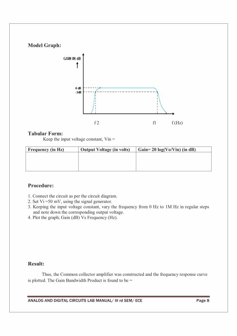
Model Graph:
f 2 f1 f (Hz)
Tabular Form: Keep the input voltage constant, Vin =
Frequency (in Hz) Output Voltage (in volts) Gain= 20 log(Vo/Vin) (in dB)
Procedure:
1. Connect the circuit as per the circuit diagram.
2. Set Vi =50 mV, using the signal generator.
3. Keeping the input voltage constant, vary the frequency from 0 Hz to 1M Hz in regular steps
and note down the corresponding output voltage.
4. Plot the graph; Gain (dB) Vs Frequency (Hz).
Result:
Thus, the Common collector amplifier was constructed and the frequency response curve
is plotted. The Gain Bandwidth Product is found to be =

ANALOG AND DIGITAL CIRCUITS LAB MANUAL/ III rd SEM/ ECE Page 9
2. COMMON SOURCE AMPLIFIER
Aim: To find the voltage gain of a CS amplifier and to find its frequency response
Apparatus:
S.No. Name Range Quantity
1. FET BFW10 2
2. Resistor 1,1,2
3. Capacitor 1.59nf, 0.578µf 2,1
4. Regulated power supply (0-30)V 1
5. Function Generator (0-3) MHz 2
6. CRO 30 MHz 1
7. Bread Board 1
Circuit Diagram:
Theory: The CS amplifier is a small signal amplifier. For good bias stability, the source resistor
voltage drop should be as large as possible. Where the supply voltage is small, Vs may be
reduced to a minimum to allow for the minimum level of Vds.R2 is usually selected as 1M or
less as for BJT capacitor coupled circuit, coupling and bypass capacitors should be selected to
have the smallest possible capacitance values. The largest capacitor in the circuit sets the circuit

ANALOG AND DIGITAL CIRCUITS LAB MANUAL/ III rd SEM/ ECE Page 10
low 3dB frequency (capacitor C2). Generally to have high input impedance FET is used. As in
BJT circuit RL is usually much larger than Zo and Zi is often much larger than Rs.
Procedure: 1. Connect the circuit as per the circuit diagram.
2. Give 1 KHz signal and 25 mv (P-P) as Vs from signal generator.
3. Observe the output on CRO for proper working of the amplifier.
4. After ensuring the amplifier function, vary signal frequency from 50 Hz to 600 Hz in proper
steps for 15-20 readings keeping Vs =25mv(PP) at every frequency ,note down the resulting
output voltage and tabulate in a table.
5. Calculate gain in dB and plot on semi log graph paper for frequency Vs gain in dB.
Tabular Form: Input voltage =
S.No Frequency Output
Voltage(Vo)
Gain Av=Vo/Vi Gain In Db
20 Log Gain
Model Graph:
Result:
Thus, the voltage gain and frequency response of a CS amplifier was measured.
ANALOG AND DIGITAL CIRCUITS LAB MANUAL/ III rd SEM/ ECE Page 11
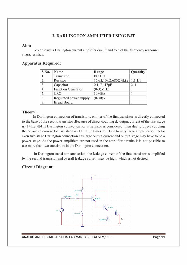
3. DARLINGTON AMPLIFIER USING BJT
Aim: To construct a Darlington current amplifier circuit and to plot the frequency response
characteristics.
Apparatus Required:
S.No. Name Range Quantity
1. Transistor BC 107 1
2. Resistor 1,1,1,1
3. Capacitor 2, 1
4. Function Generator (0-3)MHz 1
5. CRO 30MHz 1
6. Regulated power supply (0-30)V 1
7. Bread Board 1
Theory: In Darlington connection of transistors, emitter of the first transistor is directly connected
to the base of the second transistor .Because of direct coupling dc output current of the first stage
is (1+hfe )Ib1.If Darlington connection for n transitor is considered, then due to direct coupling
the dc output current foe last stage is (1+hfe ) n times Ib1 .Due to very large amplification factor
even two stage Darlington connection has large output current and output stage may have to be a
power stage. As the power amplifiers are not used in the amplifier circuits it is not possible to
use more than two transistors in the Darlington connection.
In Darlington transistor connection, the leakage current of the first transistor is amplified
by the second transistor and overall leakage current may be high, which is not desired.
Circuit Diagram:

ANALOG AND DIGITAL CIRCUITS LAB MANUAL/ III rd SEM/ ECE Page 12
Model Graph:
f2 f1 f (Hz)
Tabular Form: Keep the input voltage constant, Vin =
Frequency (in Hz) Output Voltage (in volts) Gain= 20 log(Vo/Vin) (in dB)
Procedure:
1. Connect the circuit as per the circuit diagram.
2. Set Vi =50 mv, using the signal generator.
3. Keeping the input voltage constant, vary the frequency from 0 Hz to 1M Hz in regular steps
and note down the corresponding output voltage.
4. Plot the graph; Gain (dB) vs Frequency(Hz).
5. Calculate the bandwidth from the graph.
Result:
Thus, the Darlington current amplifier was constructed and the frequency response curve
is plotted. . The Gain Bandwidth Product is found to be =
ANALOG AND DIGITAL CIRCUITS LAB MANUAL/ III rd SEM/ ECE Page 13
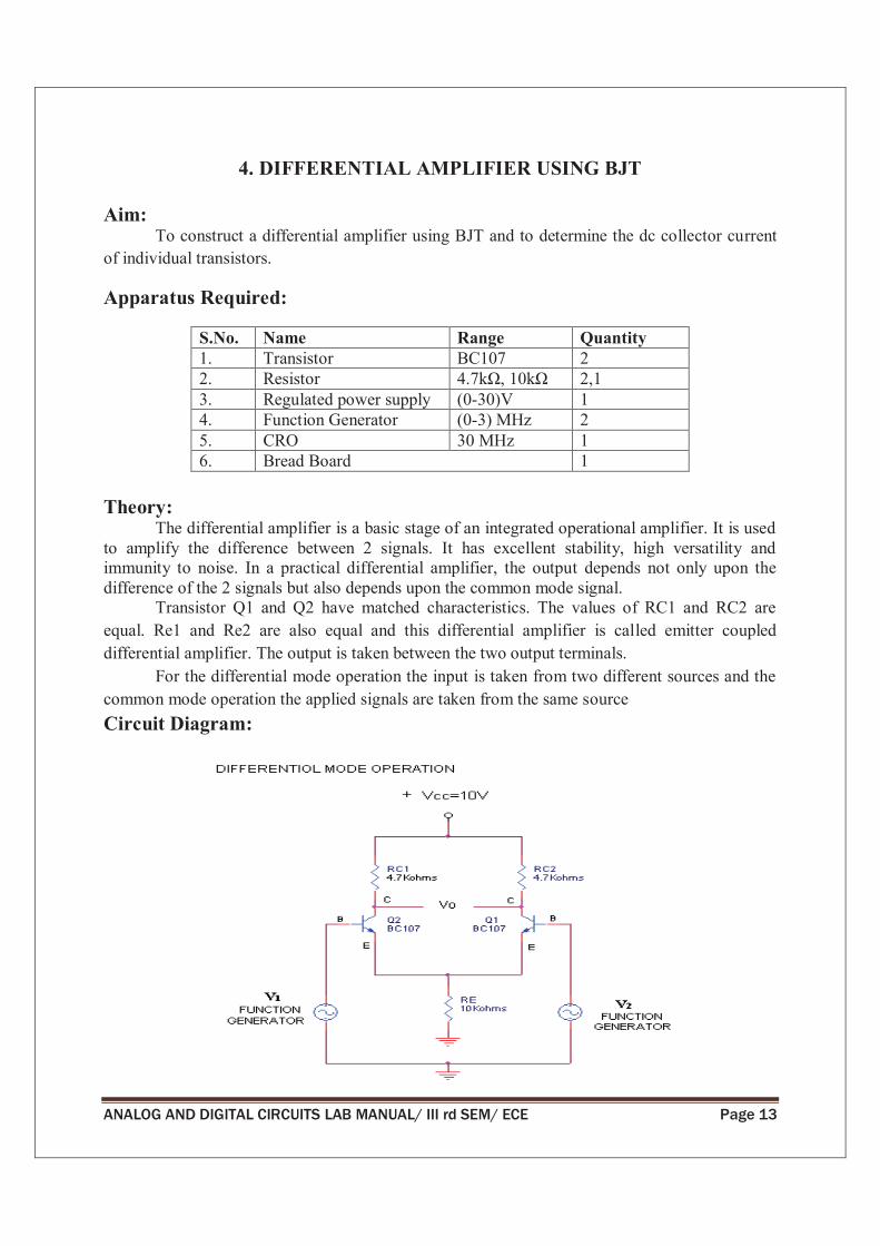
4. DIFFERENTIAL AMPLIFIER USING BJT
Aim: To construct a differential amplifier using BJT and to determine the dc collector current
of individual transistors.
Apparatus Required:
S.No. Name Range Quantity
1. Transistor BC107 2
2. Resistor 2,1
3. Regulated power supply (0-30)V 1
4. Function Generator (0-3) MHz 2
5. CRO 30 MHz 1
6. Bread Board 1
Theory: The differential amplifier is a basic stage of an integrated operational amplifier. It is used
to amplify the difference between 2 signals. It has excellent stability, high versatility and
immunity to noise. In a practical differential amplifier, the output depends not only upon the
difference of the 2 signals but also depends upon the common mode signal.
Transistor Q1 and Q2 have matched characteristics. The values of RC1 and RC2 are
equal. Re1 and Re2 are also equal and this differential amplifier is called emitter coupled
differential amplifier. The output is taken between the two output terminals.
For the differential mode operation the input is taken from two different sources and the
common mode operation the applied signals are taken from the same source
Circuit Diagram:

ANALOG AND DIGITAL CIRCUITS LAB MANUAL/ III rd SEM/ ECE Page 14
Observation:
VIN =VO =AC = VO / VIN
VIN = V1 V2
V0 =
Ad = V0/ VIN
Procedure: 1. Connections are given as per the circuit diagram.
2. To determine the common mode gain, we set input signal with voltage Vin=2V and determine
Vo at the collector terminals. Calculate common mode gain, Ac=Vo/Vin.
3. To determine the differential mode gain, we set input signals with voltages V1 and V2.
Compute Vin=V1-V2 and find Vo at the collector terminals. Calculate differential mode gain,
Ad=Vo/Vin.
4. Calculate the CMRR=Ad/Ac.
5. Measure the dc collector current for the individual transistors.
Result:
Thus, the Differential amplifier was constructed and dc collector current for the
individual transistors is determined.
ANALOG AND DIGITAL CIRCUITS LAB MANUAL/ III rd SEM/ ECE Page 15
5. DIFFERENTIAL AMPLIFIER USING BJT
Aim: To construct a differential amplifier using BJT and to calculate the CMRR.
Apparatus Required:
S.No. Name Range Quantity
1. Transistor BC107 2
2. Resistor 2,1
3. Regulated power supply (0-30)V 1
4. Function Generator (0-3) MHz 2
5. CRO 30 MHz 1
6. Bread Board 1
Formula: Common mode Gain (Ac) = VO / VIN
Differential mode Gain (Ad) = V0 / VIN
Where VIN = V1 V2
Common Mode Rejection Ratio (CMRR) = Ad/Ac
Where, Ad is the differential mode gain
Ac is the common mode gain.
Theory: The differential amplifier is a basic stage of an integrated operational amplifier. It is used
to amplify the difference between 2 signals. It has excellent stability, high versatility and
immunity to noise. In a practical differential amplifier, the output depends not only upon the
difference of the 2 signals but also depends upon the common mode signal.
Transistor Q1 and Q2 have matched characteristics. The values of RC1 and RC2 are
equal. Re1 and Re2 are also equal and this differential amplifier is called emitter coupled
differential amplifier. The output is taken between the two output terminals.
For the differential mode operation the input is taken from two different sources and the
common mode operation the applied signals are taken from the same source
Common Mode Rejection Ratio (CMRR) is an important parameter of the differential
amplifier. CMRR is defined as the ratio of the differential mode gain, Ad to the common mode
gain, Ac.
CMRR = Ad / Ac
In ideal cases, the value of CMRR is very high.

ANALOG AND DIGITAL CIRCUITS LAB MANUAL/ III rd SEM/ ECE Page 16
Circuit Diagram:
Observation:
VIN =VO =AC = VO / VIN
VIN = V1 V2
V0 =
Ad = V0/ VIN
Procedure: 1. Connections are given as per the circuit diagram.
2. To determine the common mode gain, we set input signal with voltage Vin=2V and determine
Vo at the collector terminals. Calculate common mode gain, Ac=Vo/Vin.
3. To determine the differential mode gain, we set input signals with voltages V1 and V2.
Compute Vin=V1-V2 and find Vo at the collector terminals. Calculate differential mode gain,
Ad=Vo/Vin.
4. Calculate the CMRR=Ad/Ac.
5. Measure the dc collector current for the individual transistors.
Result:
Thus, the Differential amplifier was constructed and the CMRR is calculated.

ANALOG AND DIGITAL CIRCUITS LAB MANUAL/ III rd SEM/ ECE Page 17
6. CASCODE AMPLIFIER
Aim: To measure voltage gain, input resistance and output resistance of cascade Amplifier.
Apparatus:
S.No. Name Range Quantity
1. Transistor BC107 2
2. Resistor 1 0 2,1 ,1,2
3. Capacitor 1µf,47µf 3,1
4. Regulated power supply (0-30)V 1
5. Function Generator (0-3) MHz 1
6. CRO 30 MHz 1
7. Bread Board 1
Circuit Diagram:
Theory: Cascode amplifier is a cascade connection of a common emitter and common base
amplifiers. It is used for amplifying the input signals. The common application of cascade
amplifier is for impedance matching. The low impedance of CE age is matched with the medium
of the CB sage.
Procedure: 1. Connect the circuit as per the circuit diagram.
2. Set Vi =50 mV, using the signal generator.
ANALOG AND DIGITAL CIRCUITS LAB MANUAL/ III rd SEM/ ECE Page 18
3. Keeping the input voltage constant, vary the frequency from 0 Hz to 1M Hz in regular steps
and note down the corresponding output voltage.
4. Calculate the voltage gain, input resistance and output resistance of cascade Amplifier.
Design: IB1=VCE-VBE/RB1
IC1=IE2=IC2=ßIB1
VC1=VE2=VB2-VBE
VC2=VCC-IC2*RC2
VCE2=VC2-VE2
Rin=RB1 ß1RE1
Av1=-RL1/RE1=-1
Ro=RC2
RL2=RC2 RL
AV2=RL2/RE2
Av=AV1*AV2
Result:
Thus, the voltage gain, input resistance and output resistance of cascade Amplifier was
measured.

ANALOG AND DIGITAL CIRCUITS LAB MANUAL/ III rd SEM/ ECE Page 19
7. DETERMINATION OF BANDWIDTH OF SINGLE STAGE AND
MULTISTAGE AMPLIFIERS
Aim: To determine the bandwidth of Single Stage and Multistage Amplifiers.
Apparatus:
S.No. Name Range Quantity
1. FET , Transistor BFW10 , BC107 1,2
2. Resistor 1,1,2 ,4,2,2
3. Capacitor 1.59nf, 0.578µf,10µf,100µf 2,1,3,2
4. Regulated power supply (0-30)V 1
5. Function Generator (0-3) MHz 2
6. CRO 30 MHz 1
7. Bread Board 1
Circuit Diagram:
Single Stage Common Source Amplifier Multistage Amplifier
Theory: The CS amplifier is a small signal amplifier. For good bias stability, the source resistor
voltage drop should be as large as possible. Where the supply voltage is small, Vs may be
reduced to a minimum to allow for the minimum level of Vds.R2 is usually selected as 1M or
less as for BJT capacitor coupled circuit, coupling and bypass capacitors should be selected to
have the smallest possible capacitance values. The largest capacitor in the circuit sets the circuit

ANALOG AND DIGITAL CIRCUITS LAB MANUAL/ III rd SEM/ ECE Page 20
low 3dB frequency (capacitor C2). Generally to have high input impedance FET is used. As in
BJT circuit RL is usually much larger than Zo and Zi is often much larger than Rs.
Procedure: 1. Connect the circuit as per the circuit diagram.
2. Give 1 KHz signal and 25 mv (P-P) as Vs from signal generator.
3. Observe the output on CRO for proper working of the amplifier.
4. After ensuring the amplifier function, vary signal frequency from 50 Hz to 600 Hz in proper
steps for 15-20 readings keeping Vs =25mv(PP) at every frequency ,note down the resulting
output voltage and tabulate it.
Model Graph:
Result:
Thus, the bandwidth of Single Stage and Multistage Amplifier was determined.
ANALOG AND DIGITAL CIRCUITS LAB MANUAL/ III rd SEM/ ECE Page 21
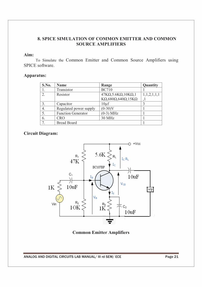
8. SPICE SIMULATION OF COMMON EMITTER AND COMMON
SOURCE AMPLIFIERS
Aim:
To Simulate the Common Emitter and Common Source Amplifiers using
SPICE software.
Apparatus:
S.No. Name Range Quantity
1. Transistor BC710 1
2. Resistor 1,1,2,1,1,1
,1
3. Capacitor 10µf 3
4. Regulated power supply (0-30)V 1
5. Function Generator (0-3) MHz 1
6. CRO 30 MHz 1
7. Bread Board 1
Circuit Diagram:
Common Emitter Amplifiers

ANALOG AND DIGITAL CIRCUITS LAB MANUAL/ III rd SEM/ ECE Page 22
Common Source Amplifiers
Theory:
Common Emitter Amplifiers
The CE amplifier is a small signal amplifier. This small signal amplifier accepts low
voltage ac inputs and produces amplified outputs. A single stage BJT circuit may be employed as
a small signal amplifier; has two cascaded stages give much more amplification. Designing for a
particular voltage gain requires the use of a ac negative feedback to stabilize the gain. For good
bias stability, the emitter resistor voltage drop should be much larger than the base -emitter
voltage. And Re resistor will provide the required negative feedback to the circuit. CE is
provided to provide necessary gain to the circuit. All bypass capacitors should be selected to
have the smallest possible capacitance value, both to minimize the physical size of the circuit for
economy. The coupling capacitors should have a negligible effect on the frequency response of
the circuit.
Common Source Amplifiers
The D.C biasing in common collector is provided by R1, R2 and RE .The load resistance
is capacitor coupled to the emitter terminal of the transistor.
When a signal is applied to the base of the transistor, VB is increased and decreased as
the signal goes positive and negative, respectively. Considering VBE is constant the variation in
ANALOG AND DIGITAL CIRCUITS LAB MANUAL/ III rd SEM/ ECE Page 23
the VB appears at the emitter and emitter voltage VE will vary same as base voltage VB . Since
the emitter is output terminal, it can be noted that the output voltage from a common collector
circuit is the same as its input voltage. Hence the common collector circuit is also known as an
emitter follower.
Procedure for Common Emitter Amplifiers: 1. Connect the circuit as per the circuit diagram.
2. Give l00Hz signal and 20mv p-p as Vs from the signal generator
3. Observe the output on CRO and note down the output voltage.
4. Keeping input voltage constant and by varying the frequency in steps 100Hz-1MHz, note
down the corresponding output voltages.
5. Calculate gain in dB and plot the frequency response on semi log sheet
Procedure for Common Source Amplifiers: 1. Connect the circuit as per the circuit diagram.
2. Set Vi =50 mV, using the signal generator.
3. Keeping the input voltage constant, vary the frequency from 0 Hz to 1M Hz in regular steps
and note down the corresponding output voltage.
4. Plot the graph; Gain (dB) Vs Frequency (Hz).
Result:
Thus, the Common Emitter and Common Source Amplifiers are simulated
using SPICE software.
ANALOG AND DIGITAL CIRCUITS LAB MANUAL/ III rd SEM/ ECE Page 24
DIGITAL EXPERIMENTS