Adaptive Signal to Noise Ratio Scalable Analog Front-End Continuous … · · 2011-08-12Adaptive...
71
Adaptive Signal to Noise Ratio Scalable Analog Front-End Continuous Time Sigma Delta Converter For Digital Hearing Aids by Ilker Deligoz A Dissertation Presented in Partial Fulfillment of the Requirements for the Degree Doctor of Philosophy Approved November 2010 by the Graduate Supervisory Committee: Sayfe Kiaei, Chair Bertan Bakkaloglu Bahar Jalali-Farahani James Aberle Junseok Chae ARIZONA STATE UNIVERSITY December 2010
Transcript of Adaptive Signal to Noise Ratio Scalable Analog Front-End Continuous … · · 2011-08-12Adaptive...
Adaptive Signal to Noise Ratio Scalable
Analog Front-End Continuous Time Sigma Delta Converter
For Digital Hearing Aids
by
Ilker Deligoz
A Dissertation Presented in Partial Fulfillment
of the Requirements for the Degree
Doctor of Philosophy
Approved November 2010 by the
Graduate Supervisory Committee:
Sayfe Kiaei, Chair
Bertan Bakkaloglu
Bahar Jalali-Farahani
James Aberle
Junseok Chae
ARIZONA STATE UNIVERSITY
December 2010

i
ABSTRACT
A dual-channel directional digital hearing aid (DHA) front end using
Micro Electro Mechanical System (MEMS) microphones and an adaptive-power
analog processing signal chain is presented. The analog front end consists of a
double differential amplifier (DDA) based capacitance to voltage conversion
circuit, 40dB variable gain amplifier (VGA) and a continuous time sigma delta
analog to digital converter (CT - Σ∆ ADC). Adaptive power scaling of the 4th
order CT - Σ∆ achieves 68dB SNR at 120µW, which can be scaled down to 61dB
SNR at 67µW. This power saving will increse the battery life of the DHA.

ii
DEDICATION
I dedicate this dissertation to my family, especially my mother and father
for their infinite support and sacrifice. To my wife for inspiring me.

iii
TABLE OF CONTENTS
Page
LIST OF TABLES ....................................................................................................... v
LIST OF FIGURES .................................................................................................... vi
CHAPTER
I. INTRODUCTION ................................................................................................. 1
A. Digital Hearing Aid System Architecture ............................................ 4
B. Front-End System Architecture and Requirements ............................. 6
C. Contributions: Adaptive Power Scaling of ADC ................................. 7
D. Organization of the Thesis .................................................................. 10
II. OVERVIEW OF ANALOG TO DIGITAL CONVERTERS USED AT DHA
SYSTEMS ........................................................................................................... 11
A. Pipeline ADCs .................................................................................... 11
B. Σ∆ ADCs ............................................................................................. 12
C. ADCs Used At DHA Literature ......................................................... 14
III. SYSTEM DESIGN AND DEVELOPMENT OF 4TH
ORDER CT - Σ∆ ADC 17
A. Discrete Time Model .......................................................................... 18
B. Discrete To Continuous Transformation............................................ 19
C. Excess Loop Delay and Jitter ............................................................. 20
IV. CIRCUIT DESIGN AND IMPLEMENTATION OF THE CT - Σ∆
MODULATOR ................................................................................................... 25
A. Integrator Circuit Architectures .......................................................... 25

iv
CHAPTER Page
B. Adaptive Active RC Integrator for Input Stage ................................. 27
C. Circuit for gm-C Integrator .................................................................. 30
D. Circuit for Σ∆ NTF Zero gm-Z ............................................................. 31
E. Feedback Loop DAC .......................................................................... 32
F. Σ∆ Comparator and Control / Timing Circuits .................................. 37
V. ADAPTIVE SNR INPUT STAGE ..................................................................... 42
A. Noise – Power Scaling ........................................................................ 42
B. Switching Transients .......................................................................... 44
VI. IC DESIGN AND MEASUREMENTS ............................................................. 46
VII. ......... CONCLUSION AND FUTURE WORKS .............................................. 50
REFERENCES .......................................................................................................... 51
APPENDIX ................................................................................................................ 54
I. ....... Analog to Digital Conversion ................................................................... 54
II. ...... SQNR Calculation of Σ∆ ADCs ............................................................... 60

v
LIST OF TABLES
Table Page
I Design Objectives for Hearing Aids. .....................................................................6
II Power scaling for quite and noisy environments. ................................................8
III Literature Comparison of Σ∆ ADCs for DHA. .................................................16
IV Power / SNR scaling of the Active RC integrator. ...........................................30

vi
LIST OF FIGURES
Figure Page
1 DHA System Block Diagram................................................................................2
2 Auditory threshold of a healthy human and speech spectrum. .............................5
3 Implemented DHA Architecture. ..........................................................................7
4 Spectrum of voice in quite environment ...............................................................9
5 Spectrum of voice in noisy environment ............................................................10
6 Pipeline ADC Architecture. ................................................................................11
7 Σ∆ ADC Architecture .........................................................................................12
8 Linearized Model of Σ∆ Modulator ....................................................................13
9 Theoretical SQNR of mth
order Σ∆ Modulator ...................................................14
10 Discrete Time Prototype. ..................................................................................18
11 NTF and STF of the Discrete Time Prototype. .................................................19
12 CT Verilog Model. ............................................................................................20
13 Integrator DC Gain vs SQNR ...........................................................................20
14 Model of discrete time and CT - Σ∆ Modulator. ..............................................21
15 CT - Σ∆ loop, with enphasis on the feedback dac ............................................22
16 Clock signals used in the Σ∆ modulator. ..........................................................23
17 SNR degradation due to the jitter......................................................................24
18 Implemented CT - Σ∆ Modulator. ....................................................................25
19 (a) Active RC integrator (b) gm-C integrator ....................................................26

vii
Figure Page
20 Folded Cascode OTA. .......................................................................................28
21 Noise Performance of Adaptive Active RC implementation. ...........................29
22 gm Circuit Schematic. ........................................................................................31
23 gm-Z transconductance stage. .............................................................................32
24 Complementary Return to Zero DAC Architecture. .........................................33
25 Dynamic Current Calibration ............................................................................35
26 Implemented DAC1 ..........................................................................................36
27 Implemented DAC2, DAC3, DCA4 .................................................................37
28 Three Level Quantizer Architecture. ................................................................39
29 The schematic of the Quantizer. .......................................................................39
30 Clock Timing Diagram. ....................................................................................40
31 Non-Overlapping Clock Generator Circuit. ......................................................40
32 Current Starved Delay Circuit. .........................................................................41
33 Small Signal Noise Model of an OTA ..............................................................43
34 Parallel connection of two OTAs ......................................................................43
35 Noise Equivalent of Two OTAs Combined. .....................................................44
36 Switching procedure of the first integrator .......................................................45
37 Micrograph of the dual-channel ADC and application board ...........................46
38 Measured SNR vs. input signal amplitude ........................................................47
39 Measured transfer curve of the Σ∆ ADC showing no peaking and channel gain
flatness ...................................................................................................................48

viii
Figure Page
40 Zero Input Noise Floor for Power Programming ..............................................49
41 Transient effects of dynamic power scaling .....................................................49
42 Sampling of Continuous Time Signals .............................................................54
43 Effect of Aliasing ..............................................................................................55
44 Quantization ......................................................................................................56
45 Quantization Error ............................................................................................56

1
I. INTRODUCTION
Hearing loss is one of the most common human impairments in our time.
Adrian Davis of the British MRC Institute of Hearing research estimates at year
2015 more than seven hundred million people in the world will suffer from mild
hearing loss [1]. Depending on the severity of the hearing loss, most of these
patients can be helped by a hearing aid device. With the advances in the
Integrated System technologies, Hearing aid devices are improving in terms of
performance, size, quality and battery life. State of the art hearing aid devices are
completely in the canal (CIC), where as the full system fits inside the ear cavity.
The first generation of hearing aid devices were introduced in 1905 and were
analog devices comprising of fixed gain amplifiers [2] and the hearing loss of the
patient was compensated mostly by amplifying the audio signal. The gain
compensation approach is not adequate as hearing problems require amplitude
and frequency compensation, directionality (phase, and space), and noise
reduction (not only background white noise, but frequency dependent color noise
reduction). The next generation of hearing aid devices was introduced in 1971
which implemented analog frequency compensation, by using a bank of band-
pass filters in parallel [3]. This approach improved the quality but was power
hungry and did not correct other issues (noise, directionality, differential noise
cancelation, etc.). The breakthrough in this area came around 1986 with the
development of digital hearing aids (DHA) [4] by applying digital signal

processing (DSP) methods for filtering, amplitude/
adaptive noise cancellation techniques.
Fig. 1 DHA System Block Diagram.
A typical modern
Front-End (Typically labe
Front-End. Transmitter Front
signal, and the DSP processes the signal. The digital a
microphone, which converts acoustic signal to electrical signal.
Gain Amplifier (VGA) adjusts the signal level to
the Analog to Digital Conversion (ADC)
output of the ADC is processed by the
digitally processed signal
One of the major short comings of the existing DHA is the lack of audio
recognition in a noisy environment, where the audio signal
ambient background noise.
audio sounds) interferes with the signal and
for the patients [1]. This can be
2
) methods for filtering, amplitude/frequency compensation, and
noise cancellation techniques.
DHA System Block Diagram.
DHA system is shown in Fig. 1, which consists
eled as Transmitter Frond-End), DSP, and Receiver
End. Transmitter Front-End receives the input sound signal, digitizes the
processes the signal. The digital audio signal is sensed by a
microphone, which converts acoustic signal to electrical signal. The Variable
n Amplifier (VGA) adjusts the signal level to an appropriate power level for
Analog to Digital Conversion (ADC). Finally, the digital bit stream from the
output of the ADC is processed by the DSP. The Receiver Front-End converts
signal to analog which drives the DHA speaker.
One of the major short comings of the existing DHA is the lack of audio
noisy environment, where the audio signal is saturated due to the
noise. In this environment, the background noise (other
with the signal and understanding conversation is hard
can be resolved by employing array signal processing
compensation, and
s of
nd Receiver
receives the input sound signal, digitizes the
udio signal is sensed by a
Variable
an appropriate power level for
he digital bit stream from the
End converts the
One of the major short comings of the existing DHA is the lack of audio
saturated due to the
(other
understanding conversation is hard
array signal processing

3
methods with multiple-microphone sensor arrays to reduce interference and
achieve directionality [5]-[6]. Directional DHA uses multiple microphones that
can also help in the identification of the source signal direction. For example, P.
M. Peterson in [5], used array antenna beam forming techniques to give
directionality, thus improve the sound quality of the hearing aid systems. This
paper shows that, compared to a single microphone system, two-microphone
beam former architecture achieves the same 50 percent keyword intelligibility
with 30dB lower target-to-interference ratio.
Multiple microphones using conventional electret microphones for
compact hearing aids, like Completely in the Canal (CIC) or In the Canal (ITC),
are hard to implement due to the microphone size. Human ear canal is
approximately 7 mm in diameter, assuming 1mm packaging; 5mm is left to fit
two microphones. State of the art conventional electret microphones are 2.6mm in
diameter and 2.6mm length [7]. Realistically it is not possible to fit two
microphones in an ear canal. Furthermore, Multi-microphone DHA requires
precise matching of the microphone and the analog front end (AFE) of each
channel. For 10 dB noise cancellation, the output voltage magnitude of the two
microphones (AFE) should match better than +/- 0.5 dB [5]. The size and
matching requirements makes miniature MEMS microphones very attractive for
multi microphone hearing aids

4
A. Digital Hearing Aid System Architecture
Digital hearing aids have many advantages to the analog counter parts; the
most important aspect is the high programmability, which is the customized
tuning capability for individual patient needs [8] - [11]. Another major advantage
of DHAs is implementing interfere noise reduction algorithms [12].
In order to measure the performance of the various DHA systems, we will
review the parameters to measure the quality of the signal.
Sound Pressure Level (SPL): The intensity of the sound wave is called
Sound Pressure Level which has the unit of Pascal (Pa) in SI system. SPL is
commonly used in logarithmic (dB) scale relative to the reference signal of the
lowest sound level that a healthy human can hear (20 µPa):
dBSPL 20 log( )refP P= × (1)
In order to measure the sound level logarithmic scale is used because
human hearing has a very wide range, and the sound sense in humans is in
logarithmic nature. Minimum hearable sound (hearing threshold) is a function of
frequency. Fig. 2 shows the information on the sound spectrum and human
hearing threshold. It can be seen that the hearing threshold is at its lowest at the
center frequency and it goes up both at low frequencies and high frequencies.
Regular conversational speech accrues in the frequency range of 100 Hz - 10
KHz, and amplitude range of 25 – 85 dB SPL. The hearing discomfort starts at
120 dB SPL and 140 dB SPL is the threshold of pain. The designed hearing aid is

targeted to cover the 120 dB dynamic range and the frequencies up to 10 KHz f
better hearing comfort.
Fig. 2 Auditory threshold of a healthy human and speech spectrum.
Another major concern in hearing aid design is the distortion. If the circuit
nonlinearities are high, it would be hard for the patient
conversation speech. The Total Harmonic Distortion (THD) for a hearing aid
should be less than 0.001% (
dB SPL) and above this sound level it should be less than 0.01% (
5
cover the 120 dB dynamic range and the frequencies up to 10 KHz f
Auditory threshold of a healthy human and speech spectrum.
concern in hearing aid design is the distortion. If the circuit
are high, it would be hard for the patient to understand the
conversation speech. The Total Harmonic Distortion (THD) for a hearing aid
should be less than 0.001% (-60 dB) for conversation speech sound levels (<80
dB SPL) and above this sound level it should be less than 0.01% (-40 dB).
cover the 120 dB dynamic range and the frequencies up to 10 KHz for
concern in hearing aid design is the distortion. If the circuit
to understand the
conversation speech. The Total Harmonic Distortion (THD) for a hearing aid
60 dB) for conversation speech sound levels (<80
40 dB).

6
B. Front-End System Architecture and Requirements
Table I summarizes the specifications for a hearing aid. From these
specifications requirements for each building block can be derived.
Frequency Band 300 Hz – 10 KHz
Amplitude Range
Dynamic Range
0 – 120 dB SPL
120 dB
THD
Input < 80 dB SPL
Input > 80 dB SPL
Less than 0.001% (-60 dB)
Less than 0.01% (-40 dB)
Table I Design Objectives for Hearing Aids.
The Architecture of the proposed system is shown in Fig. 3. The
architecture is a dual channel adaptive Power and Signal-to-Noise Ratio (SNR)
TFE. Each channel of the TFE is consists of a MEMS microphone, Capacitance to
Voltage (C2V) Readout Circuit, a VGA, adaptive 4th
order CT - Σ∆ modulator,
the decimation filter and directional array process.

7
Fig. 3 Implemented DHA Architecture.
C. Contributions: Adaptive Power Scaling of ADC
The contribution of this thesis is development and implementation of the
power / SNR scaling of the Σ∆ ADC used. The details of the scaling architecture
are discussed in chapter 4. The scaling shows no hear-able artifacts, where the
SNR is scaled from 90 dB to 81 dB, with total power consumption from 120 µW
to 62 µW by 3 dB steps.
Received Audio Signal Dynamic range shows different characteristics at
different environments. If the received signal power and dynamic range is
reduced, the front-end ADC system is adjusted to reduce the power. Fig. 4 shows

8
the spectrum of a conversation in quiet environment. Noise floor of this waveform
is about 0 dB-SPL and dynamic range of the signal is about 65 dB-SPL. Fig. 5
shows the spectrum of the same conversation in a noisy environment. The signal
power is about 10 dB-SPL higher but the noise floor is also increased to 25 dB-
SPL, resulting in a lower dynamic range of 55dB. If we used a conventional
hearing aid, it should accommodate a signal range from 0 dB-SPL to 100 dB-SPL,
which requires a dynamic range of 100 dB. On the other hand, by adjusting the
power level, and the SNR in a noisy environment, significant power saving can be
achieved.
Conventional AFE Proposed Adaptive AFE
Quite
Environment
Noisy
Environment
Quite
Environment
Noisy
Environment
Maximum
Input Sound
Level
65 dB-SPL 80 dB-SPL 65 dB-SPL 80 dB-SPL
ADC DR 70 70 70 61
VGA Setting 10 dB 0 dB 10 dB 0 dB
Input Referred
Noise Floor 0 dB-SPL 10 dB-SPL 0dB-SPL 19 dB-SPL
Required DR 65 dB 55 dB 65 dB 55 dB
Used DR 70 dB 70 dB 70 dB 61 dB
Power Saving 0 0 0 58 µW
Table II Power scaling for quite and noisy environments.
Reducing the SNR of the DHA in a noisy environment would be seamless
to the patient. Lowering the SNR of Analog Front End (AFE) would save power,
which will increase the battery life of the DHA. On the other side, changing any
configuration of the DHA is prone to transient noises like clicking or popping

sounds, or system instability. Implementing the power/SNR scalability is a
challenge in current DHA systems.
Fig. 4 Spectrum of voice in quite environment
9
sounds, or system instability. Implementing the power/SNR scalability is a
challenge in current DHA systems.
Spectrum of voice in quite environment
sounds, or system instability. Implementing the power/SNR scalability is a

Fig. 5 Spectrum of voice in noisy environment
D. Organization of
Chapter II gives an overview of analog to digital converters (ADC) used at
DHA systems. Chapter III
ADC. Chapter IV gives details of the circuit design and implementation of the CT
- Σ∆ Modulator. Chapter V explains the adaptive SNR input stage. Chapter VI
shows the final design and measurement results. Finally chapter VII gives the
conclusion and future work
10
Spectrum of voice in noisy environment
Organization of the Thesis
Chapter II gives an overview of analog to digital converters (ADC) used at
DHA systems. Chapter III describes the system design and development of the
Chapter IV gives details of the circuit design and implementation of the CT
Modulator. Chapter V explains the adaptive SNR input stage. Chapter VI
shows the final design and measurement results. Finally chapter VII gives the
conclusion and future works for the dissertation.
Chapter II gives an overview of analog to digital converters (ADC) used at
the system design and development of the Σ∆
Chapter IV gives details of the circuit design and implementation of the CT
Modulator. Chapter V explains the adaptive SNR input stage. Chapter VI
shows the final design and measurement results. Finally chapter VII gives the

II. OVERVIEW OF
The objective of this section is to mention the literature survey for ADCs
used in DHAs. There are two types of Analog to Digital Converters (ADC) that
can be used to implement a DH
Oversampling Noise Shaped (
system should be at least 90dB, which corresponds to 15 bits of resolution
(Appendix 1). Because of the high linearity requirement of the
either Pipeline Nyquist ADC architecture or
choice for this application.
A. Pipeline ADCs
Fig. 6 Pipeline ADC Architecture.
11
OVERVIEW OF ANALOG TO DIGITAL CONVERTERS USED AT
DHA SYSTEMS
The objective of this section is to mention the literature survey for ADCs
There are two types of Analog to Digital Converters (ADC) that
plement a DHA System, which are Nyquist ADCs and
Oversampling Noise Shaped (Σ∆) ADCs. Dynamic range of the hearing aid
system should be at least 90dB, which corresponds to 15 bits of resolution
(Appendix 1). Because of the high linearity requirement of the DHA system,
either Pipeline Nyquist ADC architecture or Σ∆ ADC architecture is a good
choice for this application.
Pipeline ADCs
Pipeline ADC Architecture.
ANALOG TO DIGITAL CONVERTERS USED AT
The objective of this section is to mention the literature survey for ADCs
There are two types of Analog to Digital Converters (ADC) that
s. Dynamic range of the hearing aid
system should be at least 90dB, which corresponds to 15 bits of resolution
DHA system,
ADC architecture is a good

Pipeline ADC architecture is an iterative architecture, where the
digital code of the analog signal is calculated in several stages. Every stage uses
2 or 3 level quantizer. In the first clock cycle the MSB is quantized and the
reminder is calculated. In the second clock cycle
is repeated until all the bits are quantized
the final digital code. Fig. 6 shows a generic representation of a
architecture. The advantage of this architecture is
conversion without finishing the first conversion, which is the sampling frequency
is the clock frequency. The shortcomings of it are
cycle delay, and the unit quantizer should be as linear as the final 13 bit quantizer.
This architecture has a very big stress on analog circuit design.
B. Σ∆ ADCs
Fig. 7 Σ∆ ADC Architecture
12
Pipeline ADC architecture is an iterative architecture, where the final
digital code of the analog signal is calculated in several stages. Every stage uses
. In the first clock cycle the MSB is quantized and the
n the second clock cycle the next bit is quantized and
is repeated until all the bits are quantized. The digital sum of each stage
the final digital code. Fig. 6 shows a generic representation of a pipeline
architecture. The advantage of this architecture is: the next sample can start
hout finishing the first conversion, which is the sampling frequency
is the clock frequency. The shortcomings of it are: conversion has an ‘n’ clock
cycle delay, and the unit quantizer should be as linear as the final 13 bit quantizer.
s a very big stress on analog circuit design.
ADC Architecture
final
digital code of the analog signal is calculated in several stages. Every stage uses a
. In the first clock cycle the MSB is quantized and the
next bit is quantized and this
he digital sum of each stage generates
pipeline
the next sample can start
hout finishing the first conversion, which is the sampling frequency
‘n’ clock
cycle delay, and the unit quantizer should be as linear as the final 13 bit quantizer.

13
The linearized small signal model of a Σ∆ modulator can be seen at Fig. 8
the quantizer is modeled as a quantizer gain component and an additive white
noise contribution, where the noise contribution is mentioned at Appendix I.
Fig. 8 Linearized Model of Σ∆ Modulator
Output expression y[n] can be found from linear superposition, at the z
domain. First solution is for the signal path, i.e. “Signal Transfer Function”:
( )( )
( ) 1 ( )
q
q
H z kY zSTF
X z H z k
⋅= =
+ ⋅ (2)
For the noise contribution, i.e. “Noise Transfer Function”:
( ) 1
( ) 1 ( ) q
Y zNTF
E z H z k= =
+ ⋅ (3)
From Appendix II, the SQNR of a N bit Σ∆ ADC with order m is:
2
10 2 2 12
1
2 210 log ( )
1 1 1
12 2 1 2 1
mm
N
SQNR
m OSR
π⋅ +⋅
= ⋅
⋅ ⋅ ⋅
− ⋅ +
(4)
X[n] H(z)+-
y[n]+
e[n]
kq
Quantizer

14
Fig. 9 Theoretical SQNR of mth
order Σ∆ Modulator
The theoretical SQNR calculation of 1 bit Σ∆ ADC converters can be seen
in Fig. 9. It can be seen that as the order is increased there is a dramatic increase
at the SQNR. On the other hand, higher order modulators over 2nd order are
potentially unstable. In order to resolve this NTF should be chosen carefully,
which reduces the SQNR of this theoretical calculation.
C. ADCs Used At DHA Literature
H. G. McAllister reported the first implementation of a Digital Hearing
Aid System in IEEE Computing & Control Engineering Journal at December
1995 [8]. They used TLC32044 Voice-Band Analog Interface CMOS chip, which
0
20
40
60
80
100
120
4 8 16 32 64 128 256 512 1024
SQ
NR
OSR
m=0
m=1
m=2
m=3
m=4
m=5

15
is commercially available from Texas Instruments [13]. The ADC used is a 14 bit
DR ADC with 12.5 KHz sampling rate. The Transmitter Architecture consists of a
switch capacitor anti-aliasing filter and the ADC with internal voltage reference.
It also has a serial port interface to communicate with the DSP. The analog and
mixed signal portion of the chip, both transmitter and receiver front end,
dissipates 40 mA over +5/-5 V supply. The main shortcoming of this
implementation is the high power dissipation and the big and bulky
implementation. Also generating +5/-5 V supply from a single 1.2V zinc-air
battery would require extra hardware.
First application specific analog front end (AFE) for a DHA System is
introduced by H. Neuteboom, in IEEE Journal of Solid-State Circuits, at
November 1997 [9]. They developed a fourth order CT - Σ∆ Modulator in 0.8 um
low-threshold CMOS process. The modulator consists of a fourth order feed
forward loop filter with one bit quantizer output. They used 1024 KHz sampling
frequency and achieved 7 KHz audio signal bandwidth, and Dynamic Range of
77dB. The ADC occupies 0.66 mm2 silicon area and dissipates 110 µA over a
2.15 V supply. The output has a Total Harmonic Distortion (THD) less than -50
dB.
Another reported AFE for DHA is from D. G. Gata in IEEE Journal of
Solid-State Circuits, at December 2002 [10]. They developed a third order
discrete time Σ∆ modulator in 0.6 µm mixed signal CMOS process. The third
order modulator is a cascade of two single bit stages, second order stage followed

16
by a first order stage. It has a simple R-C anti-aliasing filter before the modulator.
They used 1.28 MHz sampling frequency and achieved 10 KHz audio signal
bandwidth and Dynamic Range of 87 dB. The ADC occupies around 0.36 mm2
silicon area and dissipates 66 µA over a 1.1 V supply. The output has a 92 dB
Signal to Distortion Ratio (SDR).
The latest reported AFE for DHA is from S. Kim in IEEE Journal of
Solid-State Circuits, at April 2006 [11]. They developed an adaptive Σ∆
Modulator in 0.25 µm CMOS process. The design has an option of second or
third order discrete time modulator, working at 1.024 MHz or 2.048 MHz option.
The design has dynamic range settings of 72, 81, 78, and 86 dB which consumes
26.4, 26.8, 35.7, and 36.7 µW respectively over 0.9 V supply. The ADC occupies
around 0.3 mm2 silicon area.
[9] [10] [11]
Supply Voltage (V) 2.15 1.1 0.9
Dynamic Range
(dB)
77 87 72 81 78 86
Power
Consumption (µW)
236.5 72.6 6.4 6.8 5.7 36.7
Area (mm2) 0.66 0.36 0.3
CMOS Technology
(µm)
0.8 0.6 0.25
Table III Literature Comparison of Σ∆ ADCs for DHA.

17
III. SYSTEM DESIGN AND DEVELOPMENT OF 4TH
ORDER CT - Σ∆
ADC
The biggest challenge of the Σ∆ modulator in the DHA architecture is
while maintaining the high SNR minimum power consumption is desired. In
discrete time modulators basic integration component is a switched capacitor
integrator. In order to satisfy the SNR requirement integrator should settle to its
final value in half the clock period, which would need high gain bandwidth
product (GBW) thus higher power consumption. Where in the CT modulator, the
loop filter works on the signal bandwidth, which results in a much smaller GBW
requirement and less power consumption [14]. Another advantage of the CT
modulators is an inherent anti-aliasing function of the loop filter. The loop filter
and DAC shape puts a null to the signal transfer function at sampling frequency
(fs), and its multiples, so any aliasing signal is going to be filtered [14]. Discrete
time modulators have a sample and hold stage at the first integrator, so if there is
an aliasing signal at fs, that would be folded over to the digitized signal, in order
to avoid this, a low-pass anti-aliasing filter should be used in these Σ∆ modulators
(Appendix 3 shows detailed comparison of CT and DT Σ∆ architectures).
In order to design the final implemented CT - Σ∆ modulator, first a
discrete time model is developed, than a discrete to continuous time conversion is
performed, and final value of the loop filter is optimized to get the best SNR.

18
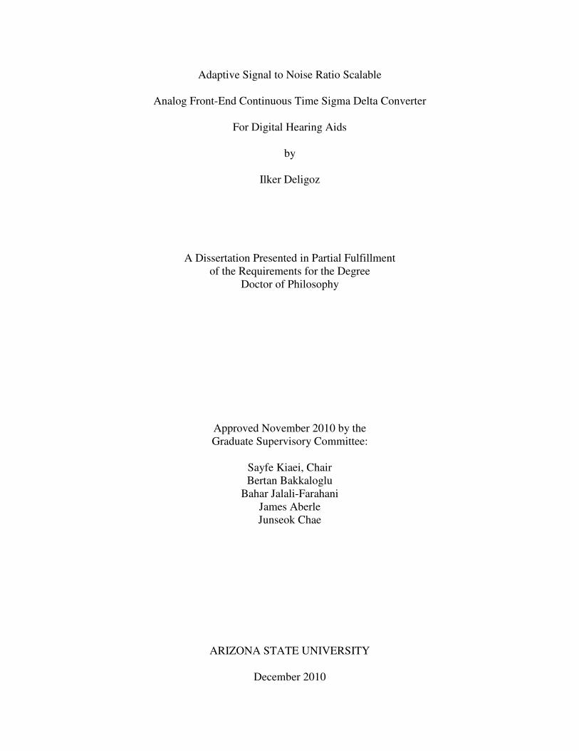
A. Discrete Time Model
Fig. 10 shows the discrete time prototype. A conventional feedback
structure with Noise Transfer Function (NTF) zero is implemented in this design
[15]. 1 MHz clock frequency is chosen to have lower switching loss at the digital
parts and DSP. A fourth order modulator gives enough SQNR to cover the 90 dB
DR required. A three level quantizer is used with Return to Zero (RZ) DAC. RZ
operation reduces the effect of excess loop delay which increases the linearity and
SQNR. NTF gain is set to 1.6 dB to increase the noise shaping which would result
in higher SQNR; the drawback of this approach is it reduces the maximum stable
input voltage to 3.6 dB lower than the quantizer reference levels. Fig. 11 shows
the NTF and STF of the designed discrete time prototype. Noise shaping and
bandwidth can be seen clearly.
Fig. 10 Discrete Time Prototype.
b1X[n] + + + +c3 c4c1 c2
a1 a2 a3 a4
gZ
- - - -
-1
z 1−
1
z 1−
1
z 1−
1
z 1−
DAC
19
Fig. 11 NTF and STF of the Discrete Time Prototype.
B. Discrete To Continuous Transformation
After the design of discrete time prototype, discrete time to continuous
time conversion is applied. Simple Euler Integration is used at each integrator. RZ
DAC scaling for the feedback coefficients is applied. The verilog model shown in
Fig. 12, is developed to validate the transformation. Lossy integrator model is
used to investigate how much DC gain is needed for the integrator. It can be seen
in Fig. 13 that a minimum gain of 60 dB is needed for the desired SQNR level.
102
103
104
105
-40
-35
-30
-25
-20
-15
-10
-5
0
5
ST
F (
Hz)
102
103
104
105
-160
-140
-120
-100
-80
-60
-40
-20
0
20
Frequency (Hz)
NT
F (
dB
)
STF
NTF
NTF
ST
F

20
Fig. 12 CT Verilog Model.
Fig. 13 Integrator DC Gain vs SQNR
C. Excess Loop Delay and Jitter
Fig. 14 shows the discrete time Σ∆ modulator and its continuous time
counterpart. The discrete time modulator and continuous time modulator are
equivalent if the error signal e[n] in both modulators is equivalent. In the signal
path this equivalency is satisfied, when an impulse-invariant transformation is
used to calculate the continuous time transfer function H(s).
x(t) b1 ∫+ c1 + ∫ c2 + ∫ c3 + ∫ c4+
∫ g2
a1
a2
a3
a4
DAC
50
60
70
80
90
100
110
20 30 40 50 60 70 80 90 100
SQ
NR
(d
B)
Integrator DC Gain (dB)

21
Fig. 14 Model of discrete time and CT - Σ∆ Modulator.
Excess loop delay analysis of CT- Σ∆ modulators are described in [16].
The CT - Σ∆ loop, with emphasis on the feedback DAC, and the clock signals
used in the Σ∆ modulator is shown in Fig. 15 and Fig. 16 respectively. C1(t) is
the clock for the comparator, and C2(t) is the clock for the RZ DAC used, C3(t) is
the Non Return to Zero (NRZ) DAC pulse. These signals are generated from a
single clock, with a non overlapping clock generator. When the C1(t) is at zero
the comparator is kept at auto zero phase, where the regenerative latch is kept at
the center point. At time T1, comparator is released; the design makes sure the
comparator latches before T2. From time T2 to T3 a quantized sampled signal is
fed back with the current steering DACs, where τ1 and τ2 are the turn on and turn

22
off time of the DAC respectively. The DAC architecture used is a return to zero
(RZ) architecture, where the DAC current is turned on after the quantizer
stabilizes, and is kept on for half a clock cycle. The DAC pulse returns back to
zero before the next sampling cycle. As a result of this clocking, this DAC
architecture does not show any excess loop delay. Because the loop is closed
before the next cycle, the Σ∆ modulator is a cycle to cycle equivalent to the
discrete counterpart.
In the NRZ case, the feedback signal is turned on and off with the
comparator output, because of the finite turn on time τ3 and the finite turn off time
of τ4, the actual current pulses are delayed from the comparator output. Because
of this delay, next sampling occurs before the full charge transfer, resulting in an
excess loop delay. Resulting in the SNR degradation and a higher signal distortion
is observed.
Fig. 15 CT - Σ∆ loop, with emphasis on the feedback DAC

23
Fig. 16 Clock signals used in the Σ∆ modulator.
The Jitter Effect in a CT - Σ∆ modulators is described in [17], the effect of
a jittery clock is the increase of the noise floor and reduction of the dynamic range
of the modulator. In a higher order Σ∆ modulator, a comparator input is
uncorrelated from the signal amplitude, as a result of this, the Jitter Effect of the
quantizer is minimal. On the other hand the jitter in the feedback DAC has a
major effect to the modulator performance. Because of the constant current in a
clock cycle is fed back to the integrators, uncertainty on the turn on and turn off

24
time of the current sources has a major effect. Fig. 17 shows the SNR
degradation due to the Jitter Effect on the designed fourth order Σ∆ modulator.
The Jitter Effect is minimal if the clock jitter is lower than 10pS.
Fig. 17 SNR degradation due to the jitter
1,000 10,000 100,000-200
-150
-100
-50
SD
Ou
tpu
t (d
bV
/Hz)
Frequency (Hz)
Jitter Performance
100 ps
10 ps
1 ps

25
IV. CIRCUIT DESIGN AND IMPLEMENTATION OF THE CT - Σ∆
MODULATOR
Nonlinearity of the first stage is not shaped by the Σ∆ loop, so high
linearity is needed at this stage. Although Active RC integrators have higher
power requirements than gm-C integrators, an active RC integrator is chosen for
the first stage. Later stage nonlinearities are suppressed by the Σ∆ loop gain, so
gm-C integrators are used for the later stages. After defining the integrator gain
from the verilog model, the coefficients a, b, c and gz are converted to resistor,
capacitor and gm values. Fig. 18 shows the implemented Σ∆ architecture.
Fig. 18 Implemented CT - Σ∆ Modulator.
A. Integrator Circuit Architectures
There are two main integrator topologies that can be used to design a CT -
Σ∆ Modulator, which are Active RC integrator and gm-C integrator. Block level
representations of these integrators can be seen in Fig. 19.

26
Fig. 19 (a) Active RC integrator (b) gm-C integrator
The basic principle of the active RC integrator is, while the OTA keeps the
input nodes at the common mode, the input voltage converts into current over the
integration resistors, and the current integrates over the integration capacitor. For
a gm-C integrator stage, input voltage is converted to current with an active
device, and integrated over the integration capacitor. Active RC integrator is a
feedback integrator on the other hand; a gm-C integrator is an open loop
integrator. Any nonlinearities of the gm device will contribute to the output
linearity directly. Nonlinearities of the active RC integrator will be divided by the
OTA open loop gain, which reduces the non-linearity of the active circuit. Also,
the active circuit noise contribution of the active RC integrator would be smaller
than the gm-C integrator.

27
B. Adaptive Active RC Integrator for Input Stage
The folded cascode OTA architecture at Fig. 20 is used as the active
device. Rp and Rn input resistors convert the voltage signal into current, and the
current is integrated over the Cp and Cn capacitors. Assuming OTA has a high
enough gain integration constant of the active RC integrator can be found as:
Vout(s) = 1/(sRC) (1)
High resistive poly resistors are used as the input resistors. MIM
capacitors are used as the integrating capacitor to increase the linearity of the
integrator. OTA is a well known folded cascode structure with a PMOS input
stage. The Input device body is connected to the source, which eliminates the
back bias effect and increases the linearity. All the devices are optimized such that
1/f corner frequency is low enough that it doesn’t affect the overall noise of the
system. Three binary scaled OTAs are designed to implement the Power / SNR
scaling, where the power consumption is 8.4 µW, 16.8 µW and 33.6 µW
respectively at 1.2 V supply. The input integration resistor is scaled by the OTA
as well. In order to increase the linearity at low power levels, a higher resistance
is used at the low power setting so the integration current is low, hence increasing
the linearity. In order to keep the loop filter unchanged, the integration capacitor
is scaled as well. The input resistor is scaled 100KΩ, 200KΩ, 400KΩ, 800KΩ
when lowering the power consumption and the integration capacitor is scaled
from 100pF, 50pF, 25pF and 12.5pF respectively.

28
Fig. 20 Folded Cascode OTA.
The smallest Active RC integrator has a 69 dB DC gain, with an
integration constant of 65.97 KRad/s.
Fig. 21 shows the input referred noise spectrum of the Active RC
integrator with enabling more OTAs in the integrator. Total current can be
changed from 7 µA to 56 µA.
Table IV shows the integrated input referred noise in the 10 KHz
bandwidth and corresponding SNR value. The effective SNR of the system can be
changed form 81 dB to 90 dB with the appropriate power setting.

29
Fig. 21 Noise Performance of Adaptive Active RC implementation.
0.E+00
2.E-07
4.E-07
6.E-07
8.E-07
1.E-06
1.E+02 1.E+03 1.E+04 1.E+05 1.E+06
Inp
ut
Re
ferr
ed
No
ise
(V
/sq
rt(H
z))
Frequency (Hz)
Noise Responce
7uA
14uA
28uA
58uA

30
Power (µW) Input Referred Noise (µVrms) SNR (dB)
67.2 6.69 90.86
33.6 9.46 87.85
16.8 13.39 84.83
8.4 18.96 81.81
Table IV Power / SNR scaling of the Active RC integrator.
C. Circuit for gm-C Integrator
The gm device converts the input voltage in to current and the current is
integrated over the effective output capacitor. The capacitor voltage is the
integration of the input voltage. The effective capacitor value can be found as a
combination of the differential capacitor and capacitors going to ground as:
Ceff = Cdiff + Cg (2)
The gm circuit at Fig. 22 is used as the voltage to current conversion. A
folded cascode structure is used to increase the integrator DC gain. A resistive
source degeneration is used to fix the transconductance value. Helper amplifiers:
Ampp and Ampn increase the linearity of the source follower where the voltages
Vinn and Vinp are generated at the two ends of the resistor. The input differential
voltage is converted into current over the Rdeg, and steered from one leg of the
input leg to the other. The differential current is copied to the output at the folding
node

31
Fig. 22 gm Circuit Schematic.
The first gm-C integrators have 69 dB DC of gain, a power dissipation of
9.6 µW over a 1.2 V supply, and the integration constants are 65.9, 103.9, 596.8
KRad/s.
D. Circuit for Σ∆ NTF Zero gm-Z
The implementation of the gm-Z puts a zero to the NTF just before the
bandwidth of the modulator, which helps to increase the SQNR of the modulator
around 20 dB. In order to get a SNR in the order of the design specification, this
NTF zero must be implemented. Because of the low frequency of operation the gm
value needed to be implemented a couple of order lower than other gm devices.
Fig. 23 shows the implemented gm-Z transconductance stage. It is a modified
version of the folded cascode transconductance stage. In order to get a low

32
transconductance value without increasing the reference resistor, a current of the
reference branch is mirrored to the desired current in three current mirroring
stages as 200:40:4:1 . As a result of this mirroring, the reference resistor is 200
times smaller than what it should be if the same transconductance stages used in
the loop filter. The gm-Z-C integrator has 42 dB DC of gain, with an integration
constant of 500 R/s. The power dissipation is 5.7 µW over 1.2 V supply.
Fig. 23 gm-Z transconductance stage.
E. Feedback Loop DAC
Current steering DACs are used due to simplify the feedback to the loop
filter. A complimentary current source and sink are used to ease requirements on
the common mode feedback circuit of the OTA and gms of the loop filter. When a
positive pulse comes from the comparator, the PMOS current source supplies
positive current to the positive integration node and the NMOS current source
sinks negative current from the negative integration node. With a negative pulse,
direction of the current sources are changed, so the PMOS current source supplies

33
to the negative integration node, and the NMOS current source sinks current from
positive integration node. For the return to zero phase the integrators are bypassed
and the PMOS current source is connected to the NMOS current source. Fig. 24
shows the simplified block diagram of the implemented RZ DAC.
Vp
Vn
VcnVcp
VcpVcn
Vbp
Vbpc
Idp
IdnVbn
Vbnc
Fig. 24 Complementary Return to Zero DAC Architecture.
In order to implement the CFFB modulator structure, four DACs are
implemented according to the feedback coefficients. DAC1 has the most stringent
requirements because it directly subtracted from the input signal. DAC1 should be
as linear as the full modulator and the noise floor should be lower than the system

34
noise floor. Dynamic current calibration and glitch minimization is used to
overcome these difficulties. Current scaling is implemented for SNR/Power
scaling as well. Fig. 25 shows a conventional dynamic calibration circuit. A bias
circuit generates gate voltages for the NMOS and PMOS current sources, but
when they are scaled up to generate the DAC currents, NMOS and PMOS scale
differently, and there is a current mismatch. In order to equate the final DAC
currents dynamic calibration is used. At the calibration phase S1 and S2 the
switches are closed. A reference current from a PMOS source flows over the fixed
current source Q1 and dynamic current source Q2. Q2 is a diode connected
device, where the extra current flows over it and sets the gate voltage. At the
regular operation S2 the switch is turned off, and the capacitor CH keeps the
calibrated gate voltage. In a conventional dynamic calibration DAC, two identical
DACs are designed. In one clock, phase one of the DACs is calibrated, and the
next phase calibrated a DAC is used in the feedback and the other DAC is set to
calibration.

Fig. 25 Dynamic Current Calibration
Fig. 26 shows the implemented
PMOS current source is calibrated. The major difference of the implemented
DAC is the calibration is done at the return to zero phase, by
extra DAC is not needed, hence saving power.
35
Dynamic Current Calibration
shows the implemented dynamic current calibration where the
PMOS current source is calibrated. The major difference of the implemented
DAC is the calibration is done at the return to zero phase, by doing it this way
extra DAC is not needed, hence saving power.
dynamic current calibration where the
PMOS current source is calibrated. The major difference of the implemented
this way

36
Vp
Vn
VcnVcp
VcpVcn
Qzp
Qzp
Qzp
Vbp
Vbpc
0.96*Idp
0.04*Idp
IdnVbn
Vbnc
Fig. 26 Implemented DAC1
Implementing DAC2, DAC3 and DAC4 does not need to be as linear as
DAC1, because the gain before each stage reduces the requirements of each DAC.
Fig. 27 show the implemented DAC structure. Dynamic current calibration is not
used, but in order for the DAC not to drift away from the common mode, a diode
divider common mode keeper circuit is used. At the zero phase, the PMOS
current source and the NMOS current source are connected together. Because of
the mismatches of the current sources, the common mode voltage at the
connection node can drift either Vdd or Vss. The diode divider sets this common

mode to a known voltage in less than half
current sources is felt into linear region. This reduces the transient glitches, which
improves the modulator stability and SQNR of the modulator.
Fig. 27 Implemented DAC2, DAC3, DCA4
F. Σ∆ Comparator
The three level (1.5 bit) quantizer
Zero phase gives a third level DAC, using a three level quantizer realizes this zero
state as a digital code, which helps the loop stability and increase of the SQNR.
The comparator architecture at
37
n voltage in less than half a clock period, such that neither of the
current sources is felt into linear region. This reduces the transient glitches, which
improves the modulator stability and SQNR of the modulator.
mented DAC2, DAC3, DCA4
Comparator and Control / Timing Circuits
hree level (1.5 bit) quantizer shown in Fig. 28 is used. The Return to
Zero phase gives a third level DAC, using a three level quantizer realizes this zero
state as a digital code, which helps the loop stability and increase of the SQNR.
he comparator architecture at Fig. 29 is used in this design, which consists of a
clock period, such that neither of the
current sources is felt into linear region. This reduces the transient glitches, which
Return to
Zero phase gives a third level DAC, using a three level quantizer realizes this zero
state as a digital code, which helps the loop stability and increase of the SQNR.
is used in this design, which consists of a

38
preamplifier and a regenerative latch. The comparator compares the input
differential signal with the differential reference voltage. When the clock to the
comparator is low, a regenerative latch is equalized, and the input signal is
compared. When the clock is high, the current differential at the output of the
preamplifier stage triggers the regenerative latch to its final value. When the input
differential voltage is greater than the reference voltage, the comparator latches
logic high, and when the input differential voltage is lower than the reference
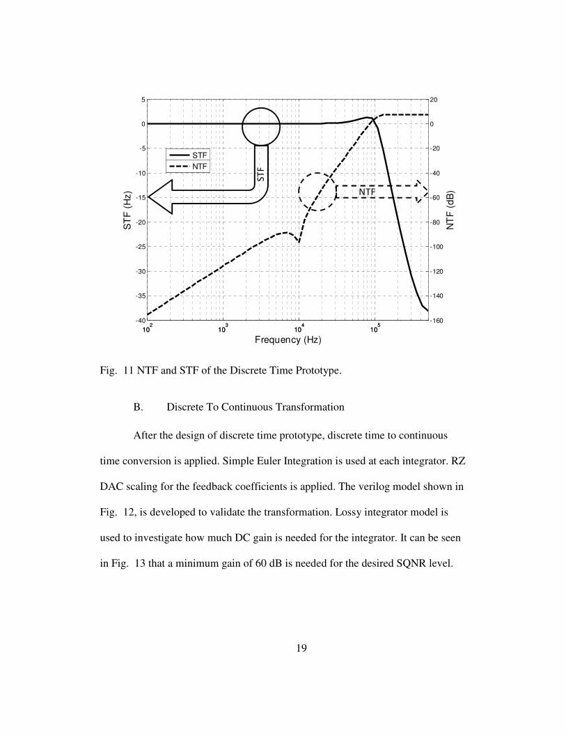
voltage, The comparator latches logic low. As shown in Fig. 30 the quantizer
uses the two phase clock. When φ1 is low the quantizer is equalized, when φ1 is
high, the output of the quantizer is latched, when φ2 is high, the output of the
quantizer is anded with the clock, which gives the return to zero phase. The major
requirement of the quantizer timing is giving enough time to the quantizer for pre-
amplification where keeping the rising edge of the φ1 before the φ2. In order to
satisfy this requirement, the non-overlapping clock generation circuit at Fig. 31 is
used. Input to this circuit is a %50 duty cycle clock, and the output is a higher
duty cycle, where the increase of the duty cycle can be found by the delay of the
NAND gates. The current starved delay architecture at Fig. 32. is used to satisfy
the requirement, the rising edge of the clock (φ1) should be later than the rising
edge of the comparator enable (φ2).

Fig. 28 Three Level Quantizer Architecture.
Fig. 29 The schematic of the Quantizer.
39
Three Level Quantizer Architecture.
The schematic of the Quantizer.
Fig. 30 Clock Timing Diagram.
CLK_IN
Fig. 31 Non-Overlapping Clock Generator Circuit.
40
Clock Timing Diagram.
Overlapping Clock Generator Circuit.
OUT_P
OUT_N

41
Fig. 32 Current Starved Delay Circuit.

42
V. ADAPTIVE SNR INPUT STAGE
Power dissipation of a Digital Hearing Aid is one of the most important
design specifications. Lower power dissipation means higher battery life, hence a
small battery can last longer. As discussed at Chapter I.C. a different SNR of the
audio signal in different environments gives flexibility to change the SNR of the
analog front end, which gives opportunity to save power in some scenarios.
A. Noise – Power Scaling
The Dynamic power / SNR scaling of continuous time filters is introduced
by Ozgun [18]. This thesis uses the same idea to scale the first integrator, which is
the major contributor of input referred noise and linearity of a CT - Σ∆ modulator.
Fig. 33 shows the small signal noise model of an OTA. The total noise of
the system can be modeled as a lumped noise source at the input. When the input
referred noise of an OTA stage is higher than the desired, by combining two
OTAs parallel, as shown at Fig. 34, the combined input referred noise gets
smaller. The input signal is the same at both amplifiers, so the output current adds
in amplitude, but the noise sources are not correlated, so the noise voltage is
summed in power at the output. As a result of this operation the output current
doubles and the output noise voltage quadruples. When we refer this to input, the
new input referred noise is half of the original one. Fig. 35 shows the noise
equivalent of this parallel architecture. This shows that the input referred noise
power of the combined system reduces by 3 dB, where the DC power dissipation

43
is doubled. Therefore in an environment when lower SNR is needed, less OTAs
are connected to reduce power in the expense of reduced system SNR.
2Vn
Fig. 33 Small Signal Noise Model of an OTA
2Vn
2Vn
Fig. 34 Parallel connection of two OTAs

44
2V
2
n
Fig. 35 Noise Equivalent of Two OTAs Combined.
B. Switching Transients
Because of the continuous nature of the input signal, there is no empty
time slot to change the power / SNR configuration of the first integrator. In order
not to have modulator instability or a hearable popping sound, one should be
careful at the transient when the parallel OTAs are connected. The best way to
connect the OTA should be: making sure the input and output nodes settle to the
active OTA in the loop. This is not reasonable because the input signal and the
feedback DAC are changing the output of the first integrator, it would require fast
tracking of the input and the output of the integrator, which would cost power and
die area. Our research shows that if we make sure the input and the output of the
first integrator is kept at the common mode, the effect of the transient is minimal
and the output of the decimated input is seamless. Fig. 36 shows the schematic of
the switching in an OTA at the active RC configuration. Before connecting the
secondary OTA to the loop both inputs are connected to common mode,

45
meanwhile the input and output are connected by transmission gate switches, so
this configuration is a unity gain configuration, where the input is zero. When the
OTA is powered up and the output is settled to common mode. Next, the input of
the OTA is disconnected from the common mode, and then the switches
connecting input to the output are turned off. Finally, the input resistor is scaled to
its final value and input and output of the secondary OTA is connected. This
power up procedure ensures the transient effect is minimal to the Σ∆ loop.
Fig. 36 Switching procedure of the first integrator

VI.
Fig. 27 shows the DHA,
CMOS process, and the MEMS microphones are fabricated in
room with custom MEMS process
frequency of 1 MHz; with an input signal bandwidth of 10KHz. Fig. 29 shows the
measured SNR against the
At the highest quiescent power setting, the CT
SNR, 65dB SNDR, and 60dB THD, respectively. Fig. 30 shows the measured
signal transfer function of the
flat over the 10 KHz bandwidth, and does not show any frequency peaking.
Fig. 37 Micrograph of the dual
46
IC DESIGN AND MEASUREMENTS
Fig. 27 shows the DHA, the analog front end is fabricated on a 0.25
CMOS process, and the MEMS microphones are fabricated in an ASU clean
room with custom MEMS processes. The CT - Σ∆ modulator has a sampling
frequency of 1 MHz; with an input signal bandwidth of 10KHz. Fig. 29 shows the
the Σ∆ modulator input amplitude at the modulator output.
At the highest quiescent power setting, the CT - Σ∆ modulator achieves 6
SNR, 65dB SNDR, and 60dB THD, respectively. Fig. 30 shows the measured
signal transfer function of the Σ∆ modulator. The measured frequency response is
flat over the 10 KHz bandwidth, and does not show any frequency peaking.
Micrograph of the dual-channel ADC and application board
end is fabricated on a 0.25µm
ASU clean
modulator has a sampling
frequency of 1 MHz; with an input signal bandwidth of 10KHz. Fig. 29 shows the
modulator input amplitude at the modulator output.
modulator achieves 68dB
SNR, 65dB SNDR, and 60dB THD, respectively. Fig. 30 shows the measured
modulator. The measured frequency response is
flat over the 10 KHz bandwidth, and does not show any frequency peaking.

Fig. 38 Measured SNR vs. input signal amplitude
103
-180
-160
-140
-120
-100
-80
-60
db
V/H
z
47
Measured SNR vs. input signal amplitude
104
105
Frequency (Hz)

48
Fig. 39 Measured transfer curve of the Σ∆ ADC showing no peaking and channel
gain flatness
Adaptive power scaling of the 4th order CT - Σ∆ achieves 68dB SNR at
120µW, which can be scaled down to 61dB SNR at 67µW. Fig. 31 shows a
measured noise level with zero input for the four power settings. The noise floor
decreases about 2-3 dB with each doubling of the first integrator power. Fig. 32
shows the transient response of the power switching. In this test the power of the
modulator is changed from minimum to maximum and vice-verse every 1ms. The
digital bit stream is then decimated and filtered with a 7th
-order digital butterwoth
filter. The output does not show dramatic artifacts (popping or clicking). This
measurement shows that when the environment changes and the DSP commands
a power level change, the modulator adapts to the change quickly, with only very
little amplitude change. An environment change will happen in a low repetition
rate, once every second or minute, the amplitude change in the output will not be
recognized by the user.
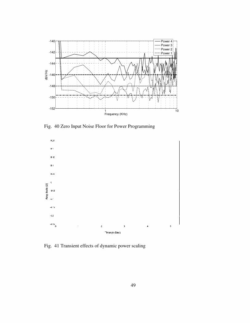
Fig. 40 Zero Input Noise Floor for Power Programming
Fig. 41 Transient effects of dynamic power scaling
-152
-150
-148
-146
-144
-142
-140
dbV
/Hz
49
Zero Input Noise Floor for Power Programming
Transient effects of dynamic power scaling
1 10Frequency (KHz)
Power 4
Power 3
Power 2
Power 1

50
VII. CONCLUSION AND FUTURE WORKS
In this thesis a power scalable Σ∆ ADC for a dual channel, transmitter
front-end digital hearing aid is presented. This system can be integrated in a
multi-chip module, which will reduce the costs of hearing aids offering superior
battery life and background noise suppression. Finally, the power scalable Σ∆
modulator shows a 68dB SNR over 10 KHz bandwidth.
The future work of this thesis is to integrate the microphone interface
circuitry, which would supply the DC bias and capacitance to the voltage
conversion of the MEMS microphone. The DSP control architecture should be
developed to find the environment condition and minimize the power dissipation.
The sensitivity of the two channels should be investigated; digital and/or analog
compensation for this mismatch should be designed to maximize the directivity of
the system.

51
REFERENCES
[1] L. M. Luxon, A. Martini, Audiological Medicine, London: Taylor &
Francis Group, 2003.
[2] The Hugh Hetherington On-line Hearing Aid Museum (n. d.) [online].
Available: http://www.hearingaidmuseum.com
[3] Trinder, E.; , "Experimental hearing-aid circuit with an input-variable
transfer function for the correction of cochlear deafness," Electronics Letters ,
vol.7, no.1, pp.2-3, January 14 1971
[4] Engebretson, A.; Morley, R.; O'Connell, M.; , "A wearable, pocket-sized
processor for digital hearing aid and other hearing prostheses applications,"
Acoustics, Speech, and Signal Processing, IEEE International Conference on
ICASSP '86. , vol.11, no., pp. 625- 628, Apr 1986
[5] P. M. Peterson, N. I. Durlach, W. M. Rabinowitz, P. M. Zurek,
“Multimicrophone adaptive beamforming for interference reduction in hearing
aids” Journal of Rehabilitation Research and Development, vol. 24 no. 4 pp.
103-110, 1987
[6] G.W. Elko, "Adaptive noise cancellation with directional microphones,"
Applications of Signal Processing to Audio and Acoustics, 1997. 1997 IEEE
ASSP Workshop on , pp.4 - 19-22, Oct 1997
[7] Knowles Microphones (n. d.) [online]. Available:
http://www.knowles.com/search/products/microphones.jsp

52
[8] H. G. McAllister, N. D. Black, N. Waterman, “Hearing aids - a
development with digital signal processing devices” IEEE Computing &
Control Engineering Journal, vol. 6, no. 6, pp. 284-291, December 1995
[9] Neuteboom, H.; Kup, B.M.J.; Janssens, M.; , "A DSP-based hearing
instrument IC," Solid-State Circuits, IEEE Journal of , vol.32, no.11, pp.1790-
1806, Nov 1997
[10] Gata, D.G.; Sjursen, W.; Hochschild, J.R.; Fattaruso, J.W.; Fang, L.;
Iannelli, G.R.; Jiang, Z.; Branch, C.M.; Holmes, J.A.; Skorcz, M.L.; Petilli,
E.M.; Chen, S.; Wakeman, G.; Preves, D.A.; Severin, W.A.; , "A 1.1-V 270-
µA mixed-signal hearing aid chip," Solid-State Circuits, IEEE Journal of ,
vol.37, no.12, pp. 1670- 1678, Dec 2002
[11] Sunyoung Kim; Jae-Youl Lee; Seong-Jun Song; Namjun Cho; Hoi-Jun
Yoo; , "An energy-efficient analog front-end circuit for a sub-1-V digital
hearing aid chip," Solid-State Circuits, IEEE Journal of , vol.41, no.4, pp.
876- 882, April 2006
[12] P. M. Peterson, N. I. Durlach, W. M. Rabinowitz, P. M. Zurek,
“Multimicrophone adaptive beamforming for interference reduction in
hearing aids” Journal of Rehabilitation Research and Development, vol. 24
no. 4 pp. 103-110, 1987
[13] TLC32044, Voice-Band Analog Interface Circuits, Texas Instruments.

53
[14] M. Ortmanns, “Continuous-time sigma-delta A/D conversion :
fundamentals, performance limits and robust implementations” New York,
Springer, 2006
[15] R. Schreier, G. C. Temes, “Understanding Delta Sigma Data Converters”,
Piscataway, NJ, IEEE Press, 2005
[16] J. A. Cherry, W. M. Snelgrove, "Excess loop delay in continuous-time
delta-sigma modulators," Circuits and Systems II: Analog and Digital Signal
Processing, IEEE Transactions on , vol.46, no.4, pp.376-389, Apr 1999
[17] Oliaei, O.; , "Clock jitter noise spectra in continuous-time delta-sigma
modulators," Circuits and Systems, 1999. ISCAS '99. Proceedings of the 1999
IEEE International Symposium on , vol.2, no., pp.192-195 vol.2, Jul 1999
[18] Ozgun, M.T.; Tsividis, Y.; Burra, G.; , "Dynamic power optimization of
active filters with application to zero-IF receivers," Solid-State Circuits, IEEE
Journal of , vol.41, no.6, pp. 1344- 1352, June 2006

I.
Analog to digital conversion is performed in two steps, first continuous
time signal is sampled according to the sampling theorem, and then the amplitude
of each sample is quantized into finite number of amplitude levels.
Any band limited continuous time signal can
time samples. Sampling can be represented on time domain by multiplying the
input signal by a pulse train with period of ‘T
corresponds to convolution with a pulse train with period of ‘fs’. Nyqui
states that if the signal is sampled at least twice the frequency of its bandwidth,
there is no distortion of the sampling.
sampling at the time and frequency domain.
Fig. 42 Sampling of Continuous Time Signals
If the signal bandwidth is more than the half sampling frequency, the
signal folds into itself and aliasing occurs. T
54
APPENDIX
Analog to Digital Conversion
digital conversion is performed in two steps, first continuous
time signal is sampled according to the sampling theorem, and then the amplitude
of each sample is quantized into finite number of amplitude levels.
Any band limited continuous time signal can be represented by its discrete
time samples. Sampling can be represented on time domain by multiplying the
input signal by a pulse train with period of ‘Ts’. This in frequency domain
corresponds to convolution with a pulse train with period of ‘fs’. Nyquist theorem
states that if the signal is sampled at least twice the frequency of its bandwidth,
there is no distortion of the sampling. Fig. 42 shows the representation of the
sampling at the time and frequency domain.
Sampling of Continuous Time Signals
the signal bandwidth is more than the half sampling frequency, the
signal folds into itself and aliasing occurs. The effect of aliasing is a distortion
digital conversion is performed in two steps, first continuous
time signal is sampled according to the sampling theorem, and then the amplitude
be represented by its discrete
time samples. Sampling can be represented on time domain by multiplying the
. This in frequency domain
st theorem
states that if the signal is sampled at least twice the frequency of its bandwidth,
he representation of the
the signal bandwidth is more than the half sampling frequency, the
he effect of aliasing is a distortion

and it cannot be reversed.
domain.
Fig. 43 Effect of Aliasing
In a digital system, there is finite number of amplitude levels to represent
each sample. In order to process the analog samples, they should be quant
Fig. 44 shows the input output relationship of a 2 bit quantizer. It can be seen that
after the quantization, there is an error term introduced. In order not to see
aliasing input signal should be filter
sampling operation.
55
reversed. Fig. 43 shows the effect of the aliasing in the frequency
Effect of Aliasing
In a digital system, there is finite number of amplitude levels to represent
each sample. In order to process the analog samples, they should be quant
shows the input output relationship of a 2 bit quantizer. It can be seen that
after the quantization, there is an error term introduced. In order not to see
aliasing input signal should be filtered with an anti-aliasing filter before the
shows the effect of the aliasing in the frequency
In a digital system, there is finite number of amplitude levels to represent
each sample. In order to process the analog samples, they should be quantized.
shows the input output relationship of a 2 bit quantizer. It can be seen that
after the quantization, there is an error term introduced. In order not to see
aliasing filter before the

Fig. 44 Quantization
If we assume the quantization error is white and uniform, the power
spectral density of the noise
density function and power spectrum of the noise.
Fig. 45 Quantization Error
56
If we assume the quantization error is white and uniform, the power
spectral density of the noise can be found easily. Fig. 45 shows the probability
density function and power spectrum of the noise.
Quantization Error
If we assume the quantization error is white and uniform, the power
shows the probability

57
The total quantization power can be calculated from the equation below
using the power density function.
2 2
e ee pdf deσ∞
−∞
= ⋅ ⋅∫ (5)
2 22 2
2
1
12e e deσ
∆
−∆
∆= ⋅ ⋅ =
∆∫ (6)
At the frequency domain, the total noise power is going to distribute from
2sf− to 2sf , so the power spectrum of the noise can be written as:
2 1( )
12e
S ffs
∆= ⋅ (7)
So for a nyquist converter Signal to Quantization Noise Ratio (SQNR) of
the ADC can be calculated as fallowing:
1
2 1N∆ =
− (8)
21
2 2sigP
=
2
2
1 1
12 12 2e N
P∆
= = ⋅ (9)
1010 log ( )sig
e
PSQNR
P= ⋅ (10)
2
102
1
2 210 log ( )
1 1( )
12 2 1N
SQNR
= ⋅
⋅−
(11)

58
1.76 6.02SQNR N= + ⋅ (12)
Where N is the number of bits used at the quantizer output. This shows
that ever one bit added to the quantizer, we gain about 6 dB at SQNR.
Because quantization error power density is inversely proportional to the
sampling frequency, if we sample the input signal with higher a frequency than
the nyquist frequency we can achieve higher SQNR. This technique is called
oversampling. Oversampling ratio (OSR) is defined as the ratio of the sampling
frequency to the nyquist frequency.
2
s
b
fOSR
f= (13)
Where, fb is the bandwidth of the input signal. If we integrate the noise
power from -fb to fb we can see the SQNR improvement:
2 1
12
b
b
f
e
f
P dffs
−
∆= ⋅∫ (14)
2 22 1
12 12
be
fP
fs OSR
∆ ⋅ ∆= ⋅ = ⋅ (15)
we can rewrite the SQNR from this noise power:
1010 log ( )sig
e
PSQNR
P= ⋅ (16)
59
2
102
1
2 210 log ( )
1 1 1( )
12 2 1N
SQNR
OSR
= ⋅
⋅ ⋅−
(17)
101.76 6.02 10 log ( )SQNR N OSR= + ⋅ + ⋅ (18)
This shows that for every doubling of the sampling frequency we get 3.01
dB better SQNR. Which also corresponds to, every quadruple of the sampling
frequency we gain an equivalent bit.

60
II. SQNR Calculation of Σ∆ ADCs
( ) 1( ) ( ) ( )
1 ( ) 1 ( )
q
q q
H z kY z X z E z
H z k H z k
⋅= ⋅ + ⋅
+ ⋅ + ⋅ (19)
For a first order Σ∆ modulator, the loop filter is a simple integrator shown
below:
1
1( )
1
zH z
z
−
−=
− (20)
Assuming the quantizer gain is unity the signal transfer function is:
1
11
1
1
1
11
z
zSTF zz
z
−
−−
−
−
−= =
+−
(21)
This is just a clock cycle delay. The noise transfer function is:
1
1
1
11
11
NTF zz
z
−
−
−
= = −
+−
(22)
This is a high pass filter. So at the low frequencies Σ∆ modulator reduces
the noise of the quantizer, which gives a higher SQNR.
If we derive the output noise power:
2
Q eP P NTF= ⋅ (23)
22
11( ) 112
b
b
f
Q
f
P z dffs
−
−
∆= ⋅ ⋅ −∫ (24)
221
( ) 4 sin ( )12
b
b
f
Q
sf
fP df
fs fπ
−
∆= ⋅ ⋅ ⋅
∫ (25)

61
Where sin( )s s
f f
f fπ π when 0
s
f
fπ ≈ , i.e. OSR >>1
22 21
( ) 4 ( )12
b
b
f
Q
sf
fP df
fs fπ
−
∆= ⋅ ⋅ ⋅
∫ (26)
32 2
2
12 3
bQ
s
fP
f
π ∆ ⋅= ⋅ ⋅
(27)
Where 2
s
b
fOSR
f=
⋅
32 2 1
12 3Q
POSR
π∆ = ⋅ ⋅
(28)
So for a 1 bit quantizer the SQNR expression can be derived as:
2
10 2 32
1
2 210 log ( )
1 1 1
12 2 1 3N
SQNR
OSR
π
= ⋅
⋅ ⋅ ⋅
−
(29)
103.4 6.02 30 log ( )SQNR N OSR= − + ⋅ + ⋅ (30)
Which means, every doubling of the OSR, SQNR increases 9 dB at a first
order Σ∆ Modulator.
For higher order modulators desired Noise Transfer Function is defined
below:
1(1 )mNTF z−= − (31)
Where, ‘m’ is the order of the modulator. The Signal Transfer Function
then becomes:

62
mSTF z
−= (32)
From this NTF, SQNR can be calculated as:
2
10 2 2 12
1
2 210 log ( )
1 1 1
12 2 1 2 1
mm
N
SQNR
m OSR
π⋅ +⋅
= ⋅
⋅ ⋅ ⋅
− ⋅ +
(33)