A Highly-Scalable Analog Equalizer Using a Tunable and ...
5
978 IEEE TRANSACTIONS ON VERY LARGE SCALE INTEGRATION (VLSI) SYSTEMS, VOL. 23, NO. 5, MAY 2015 A Highly-Scalable Analog Equalizer Using a Tunable and Current-Reusable Active Inductor for 10-Gb/s I/O Links Yong Chen, Pui-In Mak, and Yan Wang Abstract— A 0.0015-mm 2 1.28-mW single-branch analog equalizer is demonstrated in 65-nm CMOS for 10-Gb/s input/output links. Instead of using passive inductors that are untunable and unscalable with tech- nologies, gain compensation here is optimized via a tunable and current- reusable active inductor (AI). This AI incorporates a positive-feedback impedance converter with only two MOSFETs and one MOS varactor. Together with the use of: 1) negative Miller capacitors to optimize the pole-zero composition and 2) tunable resistive source degeneration to adjust the low-frequency losses, the analog equalizer recovers an eye- opening rate of minimally 30% up to 10 Gb/s over a pair of 60-cm FR4 microtrip traces. The data Pk-to-Pk jitter is <24 ps, and the RMS jitter is <4 ps, over a number of pseudorandom bit sequence patterns (2 7 –1, 2 15 –1, and 2 31 –1). Index Terms—Active inductor, analog equalizer, CMOS, eye- opening rate, jitter, negative Miller capacitor, positive-feedback. I. I NTRODUCTION High-speed input/output (I/O) links over low-cost FR4 printed circuit boards (PCBs) [1] suffer from frequency-dependent channel loss due to the skin effect and dielectric loss. A response-tunable amplifier, matching the inverse response of the channel-loss profile, can serve as the equalizer to optimize the eye opening. Most analog equalizers, such as [2], were based on a pseudodifferential common- source amplifier with resistive-capacitive source degeneration, and passive inductors at the outputs for gain-peaking and bandwidth enhancement. The former technique can easily incorporate tunable elements (e.g., MOS resistor and varactor) to control the low- frequency losses. For the high-frequency response, however, the latter is hard to be tuned, and is increasingly costly in nanoscale CMOS for its area impact, particularly in multistage designs. Although passive equalizers [3] seem more power efficient, the single-pole single-zero response is limited to slow roll-off compen- sation. Moreover, the pole-zero tuning can mainly rely on switched- capacitor banks that are bulky in size and cannot offer continuous tuning for optimal performance. This brief describes a 65-nm CMOS analog equalizer with continuously tunable low-/high-frequency responses achieved by merging resistive source degeneration and active inductor (AI) techniques in one branch. The presented AI enables wide and continuous tuning of high-frequency complex poles by a volt- age signal, simplifying the system-level adaptation while mini- Manuscript received August 17, 2013; revised April 12, 2014; accepted April 16, 2014. Date of publication May 9, 2014; date of current version April 22, 2015. This work was supported in part by the National 973 Program of China, in part by the National 863 Program of China, in part by the University of Macau under Grant MYRG114 (Y1-L4)-FST13-MPI, and in part by the Macau Science and Technology Development Fund. Y. Chen and Y. Wang are with the Institute of Microelectronics, Tsinghua University, Beijing 100084, China (e-mail: [email protected]; [email protected]). P.-I. Mak is with the State-Key Laboratory of Analog and Mixed- Signal VLSI and FST-ECE, University of Macau, Macau, China (e-mail: [email protected]). Color versions of one or more of the figures in this paper are available online at http://ieeexplore.ieee.org. Digital Object Identifier 10.1109/TVLSI.2014.2318733 Fig. 1. (a) Differential PFIC-based AI that can be merged with another circuitry to work under the same bias current. (b) Half-circuit equivalent showing the transformed admittance (Y xin ) from V xp looks into the PFIC, where V zp is terminated with a current source I b . mizing the die area and parasitics. The equalizer also measures more favorable figure of merit (FOM), area and power efficien- cies than the state of the art. The principles of positive-feedback impedance converter (PFIC) for realizing an AI is described in Section II. The proposed analog equalizer embedded such an AI is described in Section III, followed by the experimental results in Section IV. II. PFIC-BASED AI Conventional AIs were mainly relied on active or passive negative- feedback circuits [4], [5] and can involve extra power [6]. Thus, their area and power efficiencies are generally low, because a high self- resonant frequency demands a sufficient bias current to overcome the parasitic effects induced by the AI. Recently, it has been revealed that a differential AI could be more effectively emulated via a PFIC, especially for analog circuits, such as filters [7]. This brief studies, for the first time, the versatility of PFIC-based AI in the 10-GHz range, using a mainstream 65-nm CMOS process. One possible topology of PFIC-based AI is shown in Fig. 1(a). A pair of MOSFETs ( M 1 ) with cross-diode connection can transfer the capacitive effect of C AI /2 at V zp,n , into an inductive one at V xp,n . This AI topology enjoys a number of merits: 1) easy and wide inductance tunability if C AI is a MOS varactor, which has a high Q-factor in nanoscale CMOS; 2) high self- resonant frequency because of no inner parasitic poles; and 3) power efficient because it can be merged into the main circuit to reuse the bias current and avoid extra V – I and I –V conversions. To understand the admittance transfer characteristics of the AI, its half-circuit equivalent model is studied, as shown in Fig. 1(b). With V zp terminated by an ideal current source I b , the input admittance (Y xin ) at V xp can be derived Y xin ∼ = 1 R p + sC p + 1 s L AI + R s . (1) 1063-8210 © 2014 IEEE. Personal use is permitted, but republication/redistribution requires IEEE permission. See http://www.ieee.org/publications_standards/publications/rights/index.html for more information.
Transcript of A Highly-Scalable Analog Equalizer Using a Tunable and ...

978 IEEE TRANSACTIONS ON VERY LARGE SCALE INTEGRATION (VLSI) SYSTEMS, VOL. 23, NO. 5, MAY 2015
A Highly-Scalable Analog Equalizer Using a Tunable and Current-ReusableActive Inductor for 10-Gb/s I/O Links
Yong Chen, Pui-In Mak, and Yan Wang
Abstract— A 0.0015-mm2 1.28-mW single-branch analog equalizer isdemonstrated in 65-nm CMOS for 10-Gb/s input/output links. Insteadof using passive inductors that are untunable and unscalable with tech-nologies, gain compensation here is optimized via a tunable and current-reusable active inductor (AI). This AI incorporates a positive-feedbackimpedance converter with only two MOSFETs and one MOS varactor.Together with the use of: 1) negative Miller capacitors to optimize thepole-zero composition and 2) tunable resistive source degeneration toadjust the low-frequency losses, the analog equalizer recovers an eye-opening rate of minimally 30% up to 10 Gb/s over a pair of 60-cm FR4microtrip traces. The data Pk-to-Pk jitter is <24 ps, and the RMS jitteris <4 ps, over a number of pseudorandom bit sequence patterns (27–1,215–1, and 231–1).
Index Terms— Active inductor, analog equalizer, CMOS, eye-opening rate, jitter, negative Miller capacitor, positive-feedback.
I. INTRODUCTION
High-speed input/output (I/O) links over low-cost FR4 printedcircuit boards (PCBs) [1] suffer from frequency-dependent channelloss due to the skin effect and dielectric loss. A response-tunableamplifier, matching the inverse response of the channel-loss profile,can serve as the equalizer to optimize the eye opening. Most analogequalizers, such as [2], were based on a pseudodifferential common-source amplifier with resistive-capacitive source degeneration, andpassive inductors at the outputs for gain-peaking and bandwidthenhancement. The former technique can easily incorporate tunableelements (e.g., MOS resistor and varactor) to control the low-frequency losses. For the high-frequency response, however, the latteris hard to be tuned, and is increasingly costly in nanoscale CMOSfor its area impact, particularly in multistage designs.
Although passive equalizers [3] seem more power efficient, thesingle-pole single-zero response is limited to slow roll-off compen-sation. Moreover, the pole-zero tuning can mainly rely on switched-capacitor banks that are bulky in size and cannot offer continuoustuning for optimal performance.
This brief describes a 65-nm CMOS analog equalizer withcontinuously tunable low-/high-frequency responses achieved bymerging resistive source degeneration and active inductor (AI)techniques in one branch. The presented AI enables wide andcontinuous tuning of high-frequency complex poles by a volt-age signal, simplifying the system-level adaptation while mini-
Manuscript received August 17, 2013; revised April 12, 2014; acceptedApril 16, 2014. Date of publication May 9, 2014; date of current versionApril 22, 2015. This work was supported in part by the National 973 Programof China, in part by the National 863 Program of China, in part by theUniversity of Macau under Grant MYRG114 (Y1-L4)-FST13-MPI, and inpart by the Macau Science and Technology Development Fund.
Y. Chen and Y. Wang are with the Institute of Microelectronics,Tsinghua University, Beijing 100084, China (e-mail: [email protected];[email protected]).
P.-I. Mak is with the State-Key Laboratory of Analog and Mixed-Signal VLSI and FST-ECE, University of Macau, Macau, China (e-mail:[email protected]).
Color versions of one or more of the figures in this paper are availableonline at http://ieeexplore.ieee.org.
Digital Object Identifier 10.1109/TVLSI.2014.2318733
Fig. 1. (a) Differential PFIC-based AI that can be merged with anothercircuitry to work under the same bias current. (b) Half-circuit equivalentshowing the transformed admittance (Yxin) from Vxp looks into the PFIC,where Vzp is terminated with a current source Ib.
mizing the die area and parasitics. The equalizer also measuresmore favorable figure of merit (FOM), area and power efficien-cies than the state of the art. The principles of positive-feedbackimpedance converter (PFIC) for realizing an AI is described inSection II. The proposed analog equalizer embedded such an AIis described in Section III, followed by the experimental resultsin Section IV.
II. PFIC-BASED AI
Conventional AIs were mainly relied on active or passive negative-feedback circuits [4], [5] and can involve extra power [6]. Thus, theirarea and power efficiencies are generally low, because a high self-resonant frequency demands a sufficient bias current to overcomethe parasitic effects induced by the AI. Recently, it has been revealedthat a differential AI could be more effectively emulated via a PFIC,especially for analog circuits, such as filters [7]. This brief studies,for the first time, the versatility of PFIC-based AI in the 10-GHzrange, using a mainstream 65-nm CMOS process.
One possible topology of PFIC-based AI is shown in Fig. 1(a).A pair of MOSFETs (M1) with cross-diode connection can transferthe capacitive effect of CAI/2 at Vzp,n, into an inductive one atVxp,n. This AI topology enjoys a number of merits: 1) easy andwide inductance tunability if CAI is a MOS varactor, which has ahigh Q-factor in nanoscale CMOS; 2) high self- resonant frequencybecause of no inner parasitic poles; and 3) power efficient becauseit can be merged into the main circuit to reuse the bias current andavoid extra V –I and I–V conversions.
To understand the admittance transfer characteristics of the AI, itshalf-circuit equivalent model is studied, as shown in Fig. 1(b). WithVzp terminated by an ideal current source Ib, the input admittance(Yxin) at Vxp can be derived
Yxin ∼= 1
Rp+ sCp + 1
sLAI + Rs. (1)
1063-8210 © 2014 IEEE. Personal use is permitted, but republication/redistribution requires IEEE permission.See http://www.ieee.org/publications_standards/publications/rights/index.html for more information.
IEEE TRANSACTIONS ON VERY LARGE SCALE INTEGRATION (VLSI) SYSTEMS, VOL. 23, NO. 5, MAY 2015 979
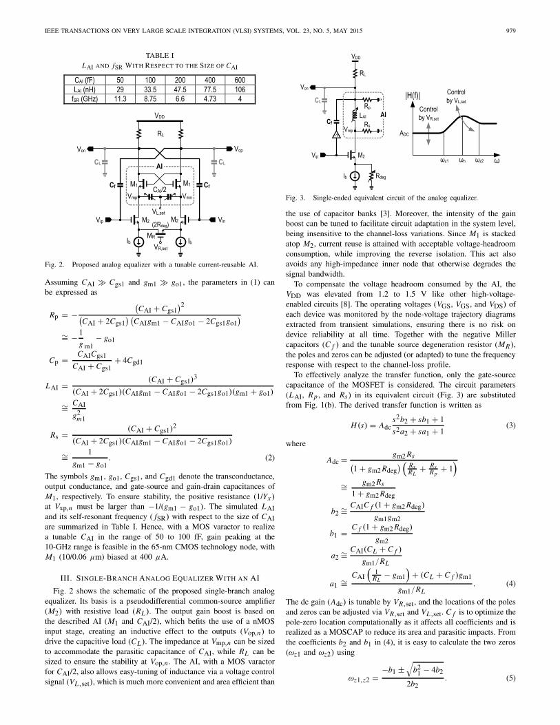
TABLE ILAI AND fSR WITH RESPECT TO THE SIZE OF CAI
Fig. 2. Proposed analog equalizer with a tunable current-reusable AI.
Assuming CAI � Cgs1 and gm1 � go1, the parameters in (1) canbe expressed as
Rp = −(CAI + Cgs1
)2
(CAI + 2Cgs1
) (CAIgm1 − CAIgo1 − 2Cgs1go1
)
∼= − 1
g m1− go1
Cp = CAICgs1
CAI + Cgs1+ 4Cgd1
LAI = (CAI + Cgs1)3
(CAI + 2Cgs1)(CAIgm1 − CAIgo1 − 2Cgs1go1)(gm1 + go1)
∼= CAI
g2m1
Rs = (CAI + Cgs1)2
(CAI + 2Cgs1)(CAIgm1 − CAIgo1 − 2Cgs1go1)
∼= 1
gm1 − go1. (2)
The symbols gm1, go1, Cgs1, and Cgd1 denote the transconductance,output conductance, and gate-source and gain-drain capacitances ofM1, respectively. To ensure stability, the positive resistance (1/Yx )at Vxp,n must be larger than −1/(gm1 − go1). The simulated LAIand its self-resonant frequency ( fSR) with respect to the size of CAIare summarized in Table I. Hence, with a MOS varactor to realizea tunable CAI in the range of 50 to 100 fF, gain peaking at the10-GHz range is feasible in the 65-nm CMOS technology node, withM1 (10/0.06 μm) biased at 400 μA.
III. SINGLE-BRANCH ANALOG EQUALIZER WITH AN AI
Fig. 2 shows the schematic of the proposed single-branch analogequalizer. Its basis is a pseudodifferential common-source amplifier(M2) with resistive load (RL). The output gain boost is based onthe described AI (M1 and CAI/2), which befits the use of a nMOSinput stage, creating an inductive effect to the outputs (Vop,n) todrive the capacitive load (CL). The impedance at Vmp,n can be sizedto accommodate the parasitic capacitance of CAI, while RL can besized to ensure the stability at Vop,n . The AI, with a MOS varactorfor CAI/2, also allows easy-tuning of inductance via a voltage controlsignal (VL ,set), which is much more convenient and area efficient than
Fig. 3. Single-ended equivalent circuit of the analog equalizer.
the use of capacitor banks [3]. Moreover, the intensity of the gainboost can be tuned to facilitate circuit adaptation in the system level,being insensitive to the channel-loss variations. Since M1 is stackedatop M2, current reuse is attained with acceptable voltage-headroomconsumption, while improving the reverse isolation. This act alsoavoids any high-impedance inner node that otherwise degrades thesignal bandwidth.
To compensate the voltage headroom consumed by the AI, theVDD was elevated from 1.2 to 1.5 V like other high-voltage-enabled circuits [8]. The operating voltages (VGS, VGS, and VDS) ofeach device was monitored by the node-voltage trajectory diagramsextracted from transient simulations, ensuring there is no risk ondevice reliability at all time. Together with the negative Millercapacitors (C f ) and the tunable source degeneration resistor (MR),the poles and zeros can be adjusted (or adapted) to tune the frequencyresponse with respect to the channel-loss profile.
To effectively analyze the transfer function, only the gate-sourcecapacitance of the MOSFET is considered. The circuit parameters(LAI, Rp , and Rs ) in its equivalent circuit (Fig. 3) are substitutedfrom Fig. 1(b). The derived transfer function is written as
H(s) = Adcs2b2 + sb1 + 1
s2a2 + sa1 + 1(3)
where
Adc = gm2 Rs(1 + gm2 Rdeg
) (RsRL
+ RsRp
+ 1)
∼= gm2 Rs
1 + gm2 Rdeg
b2 ∼= CAIC f (1 + gm2 Rdeg)
gm1gm2
b1 = C f (1 + gm2 Rdeg)
gm2
a2 ∼= CAI(CL + C f )
gm1/RL
a1 ∼=CAI
(1
RL− gm1
)+ (CL + C f )gm1
gm1/RL. (4)
The dc gain (Adc) is tunable by VR,set, and the locations of the polesand zeros can be adjusted via VR,set and VL ,set. C f is to optimize thepole-zero location computationally as it affects all coefficients and isrealized as a MOSCAP to reduce its area and parasitic impacts. Fromthe coefficients b2 and b1 in (4), it is easy to calculate the two zeros(ωz1 and ωz2) using
ωz1,z2 =−b1 ±
√b2
1 − 4b2
2b2. (5)

980 IEEE TRANSACTIONS ON VERY LARGE SCALE INTEGRATION (VLSI) SYSTEMS, VOL. 23, NO. 5, MAY 2015
Fig. 4. Simulated (a) gain response and (b) pole-zero plot with VR,set sweptfrom 0.85 to 1.25 V.
Fig. 5. Simulated (a) gain response and (b) pole-zero plot with VL ,set sweptfrom 0.5 to 1.1 V.
Fig. 6. Experimental setup for measuring the analog equalizer.
They should be sized as real zeros with different magnitudes, andcan be widely tunable via Rdeg. These conditions require
C f
CAI>
4gm2
gm1(1 + gm2 Rdeg
) . (6)
For the two poles, they should be in complex conjugate and widelytunable via VL ,set. According to the coefficients a2 and a1 in (4),the complex-pole frequency (ωn) and Q are given by
ωn =√
gm1/RL
CAI(CL + C f ), Q =
√CAI(CL+C f )
gm1/RL
(CL + C f )RL − CAI
(RL − 1
gm1
) .
(7)
Clearly, both ωn and Q are function of the tunable element 1/√
CAI.An optimal Q for the high-frequency response can minimize thephase distortion in the eye diagram [11]. From simulations, thetunability of the low-frequency losses (∼18 dB) via VR,set (0.85 to1.25 V) is shown in Fig. 4(a). For the loci of the poles and zeros, theyare plotted in Fig. 4(b) showing the variability trends. ωn is insensitiveto VR,set as expected, but still have 1 to 2 dB gain variation at highfrequency. Thus, VL ,set offers the freedom to finely adjust the high-frequency response without affecting the low-frequency one, such thatthe overall equalization can be optimized. Here, 2 to 3 dB continuousgain tunability offered by VL ,set is adequate. The gain responses and
Fig. 7. 2:1 CML selector with an embedded GAI.
Fig. 8. (a) Three-stage CML buffer with embedded two GAIs in the firstand second stages. (b) Schematic of the GAI. (c) Half-circuit equivalent.
Fig. 9. Die micrograph and zoomed views of the core layouts.
loci of the poles and zeros with respect to VL ,set (0.5 to 1.1 V)are plotted in Fig. 5(a) and (b), respectively, where VR,set is setas 0.9 V. The low-frequency zeros are almost unaffected by VL ,set.In the system level, a proper VR,set should be set first before adaptingVL ,set to optimize the performance.
IV. EXPERIMENTAL SETUP AND MEASUREMENT RESULTS
To aid testing at the 10-Gb/s range, a 2:1 current-mode-logic(CML) selector and a three-stage CML buffer were integrated withthe analog equalizer, as shown in Fig. 6. Both were designed notcontributing the equalization, but just boosting the output swing forhigh-speed testability on PCB. Confirmed by postlayout simulations,the buffer’s output essentially shows the data jitter and eye openingof the core equalizer. The data-input with different pseudorandom bitsequence (PRBS) patterns and dc bias voltages are provided by the

IEEE TRANSACTIONS ON VERY LARGE SCALE INTEGRATION (VLSI) SYSTEMS, VOL. 23, NO. 5, MAY 2015 981
TABLE IIDEVICE SIZES OF THE REALIZED ANALOG EQUALIZER
Fig. 10. Channel loss profile (Sdd21) of a pair of 60-cm microstrip traces.
Fig. 11. Measured performances of the 2:1 CML selector plus three-stageCML buffer with the GAI ON/OFF. Direct connect means just equipment toequipment. (a) Data Pk-to-Pk jitter. (b) RMS jitter.
J-BERT N4903B. The jitter and output eye diagrams were capturedvia the DSA91304A oscilloscope.
The schematics of the 2:1 CML selector and three-stage CMLbuffer are shown in Figs. 7 and 8(a), respectively. Both were embed-ded with grounded AIs (GAIs) [Fig. 8(b)], under the same principleof the PFIC as described in Section II. However, to maximize thevoltage swing and allow ON/OFF control, all GAI are not currentreuse. The GAI is equivalent to a passive network [Fig. 8(c)] witha negative resistor in parallel with a tunable lossy inductance usefulfor bandwidth extension.
The analog equalizer and its test circuitries were fabricated in65-nm CMOS. The die micrograph is shown in Fig. 9, where theanalog equalizer occupies an active area of just 0.0015 mm2. Thedevice sizes are summarized in Table II. Thanks to the single-branchstructure of the proposed equalizer having no high-impedance innernode, and the improved parasitics of the technology, a small Ib of
Fig. 12. Measured eye diagrams (left) before and (right) after equalizationat (a) 4 Gb/s and (b) 10 Gb/s under an input signal with PRBS of 231–1.
Fig. 13. Measured data Pk-to-Pk jitter and RMS jitter versus data rate underdifferent PRBS.
Fig. 14. Measured data eye-opening rate before and after equalization underdifferent PRBS.
0.426 mA is already adequate for 10-Gb/s equalization. Thus, aslong as the output swing is adequate to properly drive the back-endcircuitry, such as the D-flip flop for DFE, the proposed equalizercan be more power and area efficient, while easing the tuning ofhigh-frequency complex poles for optimal equalization.
The parasitic inductance due to the I/O is reduced to ∼600 pH bya parallel use of two bondwires, whereas the corresponding I/O bondpad adds ∼120-fF parasitic capacitance. The chip is mounted onto aFR4 PCB for chip-on-board tests with a pair of experimental 60-cmmicrostrip traces (width: 8 mils, spacing: 30 mils), which were sizedwith a differential characteristic impedance of 100 �. The measuredchannel-loss profile, including the effect of the SMA connectors, isplotted in Fig. 10. The key reference point is at 5 GHz, where thechannel loss is −16.8 dB.
The 2:1 CML selector and three-stage CML buffer with the GAION/OFF are measured first. For an input PRBS of 27–1, the 2:1 CML

982 IEEE TRANSACTIONS ON VERY LARGE SCALE INTEGRATION (VLSI) SYSTEMS, VOL. 23, NO. 5, MAY 2015
TABLE IIICHIP SUMMARY AND BENCHMARK WITH THE PRIOR ART
selector and three-stage CML buffer totally induce a data Pk-to-Pkjitter <15 ps [Fig. 11(a)], and a RMS jitter <2.6 ps [Fig. 11(b)], upto 13-Gb/s input data. These results confirm the capability of themin characterizing the proposed analog equalizer up to 10 Gb/s.
The analog equalizer has an in-band attenuation of −8.3 dB(simulation) but it is uncritical to the equalization performances [3],such as the jitter and eye opening. Yet, in the system level, theoutput signal swing should be cooptimized with the sensitivity of itsback-end circuitry, being the major concern of this equalizer whencomparing with the existing approaches. The eye diagram before andafter equalization at 4 Gb/s [Fig. 12(a)] and 10 Gb/s [Fig. 12(b)]were recorded under an input data PRBS of 231–1. Both the inputand output signal swings are ∼400 MVpp (i.e., around 150 mVppat the output of the equalizer), which is large enough to measurethe data against the environmental and equipment noises. The dataPk-to-Pk jitter (16–24 ps) and RMS jitter (3–4 ps) under 4–10 Gb/s,for a number of PRBS patterns (27–1, 215–1, and 231–1), are plottedin Fig. 13. The eye-opening rate is minimally 30% up to a 10-Gb/sdata rate (Fig. 14).
The chip summary and performance benchmark with [9]–[13] aregiven in Table III. The FOM [13] is given by (Data Rate × ChannelLoss)/Power. This brief is favorable for its improved FOM, powerand area efficiencies.
V. CONCLUSION
A 10-Gb/s single-branch analog equalizer has been reported.It features a tunable and current-reusable AI based on PFIC, mea-suring high area (0.0015 mm2) and power (1.28 mW) efficienciesin 65-nm CMOS. The easy tunability of the AI and resistive-sourcedegeneration allows the intensity of the low-frequency loss and high-frequency gain to be optimized. These beneficial features renderthis brief a superior analog equalizer candidate for cost and powerreduction of wireline systems in expensive nanoscale CMOS.
ACKNOWLEDGMENT
The authors would like to thank S. Yang for assistance and AgilentOpen Lab for measurement support.
REFERENCES
[1] A. Palaniappan and S. Palermo, “A design methodology for powerefficiency optimization of high-speed equalized-electrical I/O architec-tures,” IEEE Trans. Very Large Scale Integr. (VLSI) Syst., vol. 21, no. 8,pp. 1421–1431, Aug. 2013.
[2] J. Lee, “A 20-Gb/s adaptive equalizer in 0.13-μm CMOS technology,”IEEE J. Solid-State Circuits, vol. 41, no. 9, pp. 2058–2066, Sep. 2006.
[3] M. Hossain and A. C. Carusone, “7.4 Gb/s 6.8 mW source synchronousreceiver in 65 nm CMOS,” IEEE J. Solid-State Circuits, vol. 46, no. 6,pp. 1337–1348, Jun. 2011.
[4] M. Maeng et al., “0.18-μm CMOS equalization techniques for 10-Gb/sfiber optical communication links,” IEEE Trans. Microw. Theory Techn.,vol. 53, no. 11, pp. 3509–3519, Nov. 2005.
[5] J. Chen, F. Saibi, J. Lin, and K. Azadet, “Electrical backplane equal-ization using programmable analog zeros and folded active inductors,”IEEE Trans. Microw. Theory Techn., vol. 55, no. 7, pp. 1459–1466,Jul. 2007.
[6] H. Lee et al., “A 16 Gb/s/link, 64 Gb/s bidirectional asymmet-ric memory interface,” IEEE J. Solid-State Circuits, vol. 44, no. 4,pp. 1235–1247, Apr. 2009.
[7] A. Pirola, A. Liscidini, and R. Castello, “Current-mode, WCDMAchannel filter with in-band noise shaping,” IEEE J. Solid-State Circuits,vol. 45, no. 9, pp. 1770–1780, Sep. 2010.
[8] P.-I. Mak and R. P. Martins, “High-/mixed-voltage RF and analogCMOS circuits come of age,” IEEE Circuits Syst. Mag., vol. 10, no. 4,pp. 27–39, Dec. 2010.
[9] D. Lee, J. Han, G. Han, and S. M. Park, “10 Gbit/s 0.0065 mm2 6 mWanalogue adaptive equaliser utilising negative capacitance,” Electron.Lett., vol. 45, no. 17, pp. 863–865, Aug. 2009.
[10] J.-H. Lu, K.-H. Chen, and S.-I. Liu, “A 10-Gb/s inductorless CMOSanalog equaliser with an interleaved active feedback topology,” IEEETrans. Circuits Syst. II, Exp. Briefs, vol. 56, no. 2, pp. 97–101,Feb. 2009.
[11] S. Gondi and B. Razavi, “Equalization and clock and data recoverytechniques for 10-Gb/s CMOS serial-link receivers,” IEEE J. Solid-StateCircuits, vol. 42, no. 9, pp. 1999–2011, Sep. 2007.
[12] J.-H. Lu, C.-L. Luo, and S.-I. Liu, “A passive filter for 10-Gb/s0.18-μm CMOS technology,” in Proc. IEEE A-SSCC, Nov. 2007,pp. 404–407.
[13] M. Ganzerli, L. Larcher, S. Erba, and D. Sanzogni, “An inductor-less13.5-Gbps 8-mW analog equalizer for multi-channel multi-frequencyoperation,” in Proc. IEEE ISCAS, May 2011, pp. 189–192.