AD9161/AD9162/AD9163/AD9164 User Guide (Rev. 0)
22
AD9161/AD9162/AD9163/AD9164 User Guide UG-1526 One Technology Way • P.O. Box 9106 • Norwood, MA 02062-9106, U.S.A. • Tel: 781.329.4700 • Fax: 781.461.3113 • www.analog.com Evaluating the AD9161, AD9162, AD9163, and AD9164 High Speed, RF DACs PLEASE SEE THE LAST PAGE FOR AN IMPORTANT WARNING AND LEGAL TERMS AND CONDITIONS. Rev. 0 | Page 1 of 22 FEATURES Full featured evaluation board for the AD9161, AD9162, AD9163, and AD9164 ACE software for control Direct clocking vs. on-board clocking Showing RF modes of the DAC, including mixed mode and 2× NRZ NCO only mode JESD204B interface mode EVALUATION KIT CONTENTS AD9162-FMC-EBZ, AD9164-FMC-EBZ, AD9162-FMCB-EBZ, AD9164-FMCB-EBZ, AD9161-FMCC-EBZ, AD9162-FMCC- EBZ, AD9163-FMCC-EBZ, or AD9164-FMCC-EBZ Mini USB cable Evaluation board DVD RECOMMENDED EQUIPMENT LIST 12 V dc power supply Dual sinusoidal clock source (5 GHz, <0.5 ps rms jitter) Spectrum analyzer ADS7-V2EBZ pattern generator and data capture board GENERAL DESCRIPTION This user guide is for the AD9161, AD9162, AD9163, and AD9164 evaluation board. The evaluation board connects to an ADS7- V2EBZ pattern generator for quick evaluation of the AD9161, AD9162, AD9163, and AD9164, high speed, RF digital-to-analog converters (RF DACs). The ADS7-V2EBZ automatically formats the data and sends it to the evaluation board, which simplifies evaluation of the device. The evaluation board runs from the FPGA mezzanine card (FMC) power supply. Figure 1 shows the top side of the evaluation board. The evaluation board includes a clock buffer, the AD9508, which provides the reference clock and SYSREF± pins to the ADS7-V2EBZ, and the SYSREF± pins signal to the DAC. The evaluation board can be driven by an external clock or the on-board clock (ADF4355), as shown in Figure 2. There is a single-pole, double throw (SPDT) switch on the board for selecting the clock source. AD9161, AD9162, AD9163, AND AD9164 EVALUATION BOARD PHOTOGRAPH 20160-001 Figure 1.
Transcript of AD9161/AD9162/AD9163/AD9164 User Guide (Rev. 0)

AD9161/AD9162/AD9163/AD9164 User Guide UG-1526
One Technology Way • P.O. Box 9106 • Norwood, MA 02062-9106, U.S.A. • Tel: 781.329.4700 • Fax: 781.461.3113 • www.analog.com
Evaluating the AD9161, AD9162, AD9163, and AD9164 High Speed, RF DACs
PLEASE SEE THE LAST PAGE FOR AN IMPORTANT WARNING AND LEGAL TERMS AND CONDITIONS. Rev. 0 | Page 1 of 22
FEATURES Full featured evaluation board for the AD9161, AD9162,
AD9163, and AD9164 ACE software for control Direct clocking vs. on-board clocking Showing RF modes of the DAC, including mixed mode and 2×
NRZ NCO only mode JESD204B interface mode
EVALUATION KIT CONTENTS AD9162-FMC-EBZ, AD9164-FMC-EBZ, AD9162-FMCB-EBZ,
AD9164-FMCB-EBZ, AD9161-FMCC-EBZ, AD9162-FMCC-EBZ, AD9163-FMCC-EBZ, or AD9164-FMCC-EBZ
Mini USB cable Evaluation board DVD
RECOMMENDED EQUIPMENT LIST 12 V dc power supply Dual sinusoidal clock source (5 GHz, <0.5 ps rms jitter) Spectrum analyzer ADS7-V2EBZ pattern generator and data capture board
GENERAL DESCRIPTION This user guide is for the AD9161, AD9162, AD9163, and AD9164 evaluation board. The evaluation board connects to an ADS7-V2EBZ pattern generator for quick evaluation of the AD9161, AD9162, AD9163, and AD9164, high speed, RF digital-to-analog converters (RF DACs). The ADS7-V2EBZ automatically formats the data and sends it to the evaluation board, which simplifies evaluation of the device. The evaluation board runs from the FPGA mezzanine card (FMC) power supply.
Figure 1 shows the top side of the evaluation board. The evaluation board includes a clock buffer, the AD9508, which provides the reference clock and SYSREF± pins to the ADS7-V2EBZ, and the SYSREF± pins signal to the DAC.
The evaluation board can be driven by an external clock or the on-board clock (ADF4355), as shown in Figure 2. There is a single-pole, double throw (SPDT) switch on the board for selecting the clock source.
AD9161, AD9162, AD9163, AND AD9164 EVALUATION BOARD PHOTOGRAPH
2016
0-00
1
Figure 1.
UG-1526 AD9161/AD9162/AD9163/AD9164 User Guide
Rev. 0 | Page 2 of 22
TABLE OF CONTENTS Features .............................................................................................. 1 Evaluation Kit Contents ................................................................... 1 Recommended Equipment List ...................................................... 1 General Description ......................................................................... 1 AD9161, AD9162, AD9163, and AD9164 Evaluation Board Photograph ........................................................................................ 1 Revision History ............................................................................... 2 Evaluation Board Software .............................................................. 3 Hardware Setup ................................................................................. 4
Configuration 1 ............................................................................ 4 Configuration 2 ............................................................................ 4 Configuration 3: DC Test/NCO Mode Without ADS7-V2EBZ (Only Available for AD9162 and AD9164) ................. 4
Getting Started .................................................................................. 5 Initial Setup ................................................................................... 5
DC Test/NCO Mode (Only Available for AD9162 and AD9164) .............................................................................................6
Configure the Spectrum Analyzer ..............................................6 Configure the Evaluation Board .................................................6
Using the ADS7-V2EBZ to Play a Pattern to the Evaluation Board ...................................................................................................9
Configure Spectrum Analyzer .....................................................9 Load and Play Pattern to the ADS7-V2EBZ ..............................9 Configure the Evaluation Board .............................................. 11 Using External Files ................................................................... 14 Evaluation Boards Differences ................................................. 15 Clock Network Performance Optimization ............................ 16 ACE User Guide ......................................................................... 16 JESD204B Lane Mapping of the Evaluation Board ............... 18 Troubleshooting .......................................................................... 19
REVISION HISTORY 11/2019—Revision 0: Initial Version

AD9161/AD9162/AD9163/AD9164 User Guide UG-1526
Rev. 0 | Page 3 of 22
EVALUATION BOARD SOFTWARE The evaluation board software provides an easy to use graphical user interface called analysis, control, evaluation (ACE). ACE is included on the evaluation board DVD and is available at www.analog.com/EVAL-AD916X.
From the DVD, install the AD9161 series ACE serial peripheral interface (SPI) programmer application. Also, from the DVD (or from wiki.analog.com as a part of the DAC software suite), install the DPGDownloader™. Use this program for loading vectors into the ADS7-V2EBZ.
The ACE SPI programmer application enables full access to the register map of the AD9161, AD9162, AD9163, and AD9164, and has additional functionality, such as the ability to record, load, and save macros, or register sequences, to ease programming of the device.
The ADF4355 and AD9508 are also configured by ACE. Several macros or register sequences are included in this user guide to demonstrate the usefulness of the function and to set up the device. ACE also controls the SPDT switch for selecting the clock source.
OPTIONAL 12VSUPPLY
OPTIONALEXTERNALREFERENCE
OPTIONALDACCLOCK
CRYSTALOSCILLATOR
J61
TP41 ANDTP64
XP2USB
USB
P1
FPGA REF
SYSREF±
J31
J32
SYSREF±AD9508
÷4
ADF4355
HMC849A
HIGH SPEEDDACJESD204B
SPECTRUMANALYZERADS7-V2EBZ
2016
0-00
2
Figure 2. Block Diagram of the Evaluation Board Lab Bench Setup
FMC CONNECTOR
Y61: CRYSTALBOARD VERSION
J1: CRYSTALPOWER JUMPER
TP41: 12V POWER
TP64: GND
XP2: USB
J32: DAC OUTPUT
J31: EXTERNAL CLOCK
J61: ADF4355REF CLOCK
J62: ADF4355 OUTPUT
2016
0-00
3
Figure 3. Evaluation Board: Top Side
UG-1526 AD9161/AD9162/AD9163/AD9164 User Guide
Rev. 0 | Page 4 of 22
HARDWARE SETUP CONFIGURATION 1 Use the external signal generator as the clock source as follows:
1. Remove the jumper on JP1. 2. Connect a low phase noise, high frequency clock source to
the J31 subminiature Version A (SMA) connector. 3. Set the output level to 0 dBm. 4. Connect a second low phase noise, high frequency clock
source (10 MHz to 250 MHz) with a 0 dBm output level that is the reference clock of the ADF4355 to the J61 SMA connector.
5. Synchronize the two clock sources. A unit (such as the Rohde & Schwarz SMA100) has a convenient option for a secondary signal source. Using this option ensures that the two clocks are synchronized. The 10 MHz reference output of the signal generator can also be used as the reference input.
6. Connect the spectrum analyzer to the J32 SMA connector. 7. Connect the evaluation board to the FMC connector of the
ADS7-V2EBZ.
2016
0-00
4
Figure 4. View of the Top of the ADS7-V2EBZ Pattern Generator Board
CONFIGURATION 2 Use the on-board ADF4355 as the clock source as follows:
1. Put the jumper on JP1 (on the evaluation board). 2. Connect the spectrum analyzer to the J32 SMA connector. 3. Connect the evaluation board to the FMC connector of the
ADS7-V2EBZ. 4. Connect the ac adapter to the ADS7-V2EBZ. 5. Press the power switch on the ADS7-V2EBZ to power on
both boards.
CONFIGURATION 3: DC TEST/NCO MODE WITHOUT ADS7-V2EBZ (ONLY AVAILABLE FOR AD9162 AND AD9164) The AD9162 andAD9164 can work in dc test/NCO mode without the ADS7-V2EBZ. However, the devices need to run from an external power supply.
In this case, do not connect the evaluation board to the ADS7-V2EBZ. Instead, complete the following steps:
1. Connect a 12 V dc supply to TP41 (red) and GND to TP64 (black) on the evaluation board. The external power supply must have capacity for 1 A of current.
2. Put the jumper on JP1 if using the on-board ADF4355 as the clock source. If using an external clock source, connect a low phase noise, high frequency clock source to J31.
3. Connect the spectrum analyzer to the J32 SMA connector.

AD9161/AD9162/AD9163/AD9164 User Guide UG-1526
Rev. 0 | Page 5 of 22
GETTING STARTED The software is included in the evaluation board DVD. The installation includes an updated version of the DPGDownloader software and the necessary files for all variants of the AD9161, AD9162, AD9163, and AD9164 evaluation boards, including the schematic, board layout, data sheet, and SPI programmer. Download the DPGDownloader software online from the DAC Software Suite.
Also install the ACE software to configure the device. ACE is the software that is used to load the registers in the AD9161, AD9162, AD9163, and AD9164. The ACE software enables full access to the AD9161, AD9162, AD9163, and AD9164 register map, and has several views and features that simplify its use. Many of the ACE software features are detailed in the ACE User Guide section.
Download this software online from the ACE software page. The ACE software package includes the required plugins for the AD9161, AD9162, AD9163, and AD9164 evaluation board.
INITIAL SETUP Complete the following initial steps to get started with the evaluation of the device:
1. Install the DPGDownloader software on the PC. Analog Devices, Inc. recommends verifying the basic setup before making any modifications to the evaluation board.
2. Connect the PC to the evaluation board using the XP2 mini USB connector after installing the necessary software packages.
3. Connect the PC to the ADS7-V2EBZ using the USB connector.
Several different configurations and scenarios are explained in this user guide with step by step instructions. Choose the configuration that meets the requirements. A summary of the ACE user guide is provided in the ACE User Guide section.
UG-1526 AD9161/AD9162/AD9163/AD9164 User Guide
Rev. 0 | Page 6 of 22
DC TEST/NCO MODE (ONLY AVAILABLE FOR AD9162 AND AD9164) CONFIGURE THE SPECTRUM ANALYZER Configure the spectrum analyzer as follows:
Start frequency = 50 MHz. Stop frequency = 5 GHz. Resolution bandwidth = 300 kHz. Use average/rms
detector setting. Choose input attenuation as 6 dB. This value can be
adjusted later if indications are that the analyzer is causing degradations (warnings on the analyzer itself, or third-order products appearing on the output spectrum).
CONFIGURE THE EVALUATION BOARD Complete the following steps to configure the evaluation board to output a single tone at 1 GHz:
1. Ensure that the evaluation board is configured and powered up using an external power supply according to the Hardware Setup section.
2. Open the ACE software from Start > Programs > Analog Devices > ACE. A window appears, as shown in Figure 5.
3. Open the evaluation board view by double clicking on the AD9162-FMC-EBZ evaluation board icon as shown in Figure 5.
4. For DAC Clock Source, click ADF4355-ADCLK914 as shown in Figure 6.
5. Using the AD916x Startup Wizard on the left side of the window, complete the following steps: a. For Operation Mode, select DC Test Mode. b. Set FDAC to 2.4576 GHz. c. Select the NCO Enable box. d. Set Frequency Shift to 1 GHz. e. Set DC Back-Off(dB) to −0.1 dB. f. Click the Apply button.
A 1 GHz single tone appears on the spectrum analyzer, as shown in Figure 7.
6. Change the NCO frequency and repeat Step 3 to select a different output frequency.
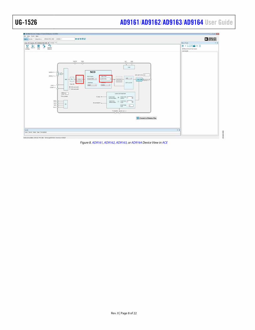
7. To avoid the start-up sequence each time, double click the AD9162-FMC-EBZ evaluation board icon to display the device view as shown in Figure 8. The device view is an interactive view of the AD9161, AD9162, AD9163, or AD9164 device that allows the user to configure more features of the device, including the NCO and the FIR85 enable, the DAC decode mode, and the clock input tuning parameters.
8. After entering a number or selecting an option or clicking on a block to enable or disable it, click the Apply Changes button in the top left corner of the window to apply the changes to the registers of the device.
2016
0-00
5
Figure 5. ACE Software Window

AD9161/AD9162/AD9163/AD9164 User Guide UG-1526
Rev. 0 | Page 7 of 22
12
3
45
6
2016
0-00
6
Figure 6. AD9161, AD9162, AD9163, and AD9164 Evaluation Board View and Clock Source Selection in ACE
2016
0-00
7
Figure 7. Spectrum Analyzer Plot of DAC Output in NCO Mode (Showing a Single Tone at 1 GHz)
UG-1526 AD9161/AD9162/AD9163/AD9164 User Guide
Rev. 0 | Page 8 of 22
2016
0-00
8
Figure 8. AD9161, AD9162, AD9163, or AD9164 Device View in ACE

AD9161/AD9162/AD9163/AD9164 User Guide UG-1526
Rev. 0 | Page 9 of 22
USING THE ADS7-V2EBZ TO PLAY A PATTERN TO THE EVALUATION BOARD CONFIGURE SPECTRUM ANALYZER Configure the spectrum analyzer as follows:
• Start frequency = 50 MHz. • Stop frequency = 5 GHz. • Resolution bandwidth = 300 kHz. • Use average/rms detector setting. • Choose input attenuation as 6 dB. This value can be
adjusted later if indications are that the analyzer is causing degradations (warnings on the analyzer itself, or third-order products appearing on the output spectrum).
LOAD AND PLAY PATTERN TO THE ADS7-V2EBZ Complete the following steps to configure the ADS7-V2EBZ board and load a single tone at 800 MHz to the on-board FPGA:
1. Configure the hardware according to the instructions provided in the Hardware Setup section.
2. To load and play the pattern to the ADS7-V2EBZ, open the DPGDownloader from Start > Programs > Analog Devices > DPG > DPGDownloader.
3. Ensure that the program detects the AD9161, AD9162, AD9163, or AD9164 and reflects the name in the Evaluation Board dropdown list. For this evaluation board, JESD204B.C is the only valid port configuration and it is selected automatically. The Line Rate field may not immediately show a clock frequency.
4. In the lower portion of the screen, choose Subclass 0 from the Subclass dropdown menu. The SYNC Status may show a green check mark or a red cross. See Figure 9.
2016
0-00
9
Figure 9. DPGDownloader Configuration for the AD9161, AD9162, AD9163, and AD9164

UG-1526 AD9161/AD9162/AD9163/AD9164 User Guide
Rev. 0 | Page 10 of 22
5. Select Add Generated Waveform > Single Tone, as shown in Figure 10. A single tone panel is added to the vector list.
6. Enter 2.458 GHz in Data Rate (or DAC clock frequency). 7. Enter 16 bits in DAC Resolution.
The AD9161 resolution is 11 bits and the AD9162, AD9163, and AD9164 resolution is 16 bits. The AD9161 can receive either 16-bit or 11-bit data because the JESD204B data packing engine packs data in 8-bit sizes. If 11-bit data is chosen, the DPGDownloader software zero-pads the data words to create 16-bit words for transfer to the data framer. Because the AD9161 data path is 16 bits, Analog Devices recommends sending 16-bit data to the device so that true 16-bit math is computed with truncation happening prior to the DAC decoder. Sending 16-bit data this way can improve spurious performance as compared to sending 11-bit data.
8. Enter 800 MHz in Desired Frequency. 9. Keep 0.0 dB in Amplitude. 10. Clear the Unsigned Data box because the AD9161,
AD9162, AD9163, and AD9164 accept only twos complement data. Ensure that Generate Complex Data (I & Q) is not selected.
11. From the Vector dropdown list, select 1Q: Single Tone – 750.122 MHz; 0.0 dB; 0.0° (Quadrature) as the data vector.
12. Leave the other options as default values. SYNC Status may show as the red X, as in Figure 11.
13. Click the down arrow button to download the pattern from the computer to the ADS7-V2EBZ unit.
14. Wait for the play button to become active, and then click the play button to begin vector playback to the evaluation board.
2016
0-01
0
Figure 10. Choose Single Tone as the Vector Type
2016
0-01
1
Figure 11. DPGDownloader: Selected Vector and Downloaded to the ADS7-V2EBZ Unit

AD9161/AD9162/AD9163/AD9164 User Guide UG-1526
Rev. 0 | Page 11 of 22
CONFIGURE THE EVALUATION BOARD After configuring the FPGA board (ADS7-V2EBZ), configure the evaluation board using the hardware. Perform the following steps:
1. Open the ACE software from Start > Programs > Analog Devices > ACE). A window appears similar to Figure 5.
2. Open the evaluation board view by double clicking on the AD9161, AD9162, AD9163, and AD9164 evaluation board icon as shown in Figure 5.
3. Using the AD916x Startup Wizard on the left side of the window, follow these steps, as shown in Figure 12:
a. Select SERDES Mode in the Operation Mode dropdown list (Label 1).
b. For DAC Clock Source, click ADF4355-ADCLK914 (Label 2).
c. Set FDAC to 2.4576 GHz (Label 3). d. Set Interpolation to 1 (Label 4). e. Set Serdes Lanes to 8 (Label 5).
Note that 8-lane is the only supported lane number for 1× interpolation (bypass) mode. The minimum interpolation ratio is 1 for the AD9162 and AD9164, 2 for the AD9161, and 6 for the AD9163.
f. Click the Apply button (Label 6) at the bottom of the AD916x Startup Wizard window.
12
345
6
2016
0-01
2
Figure 12. AD9161, AD9162, AD9163, and AD9164 Evaluation Board View and Clock Source Selection in ACE

UG-1526 AD9161/AD9162/AD9163/AD9164 User Guide
Rev. 0 | Page 12 of 22
4. Report the line rate frequency from the AD9161, AD9162, AD9163, or AD9164 in the DPGDownloader as 12.07 Gbps, as shown in Figure 13. SYNC Status shows as a green check mark. An 800 MHz single tone appears on the spectrum analyzer, as shown in Figure 14.
5. Change the frequency of the tone by enabling the NCO in the ACE board view. See Figure 12. Scroll down to the NCO Configuration section and check the NCO Enable box.
6. Set the Frequency Shift field to the desired shift frequency (in Hz).
7. Change DC Back-Off(dB) to 0 dB. This step causes the fundamental tone at 800 MHz to shift by the amount determined in the Frequency Shift field.
8. Choose a new frequency for the DPGDownloader vector generator to create and redownload the vector. The redownload may momentarily disable the JESD204B link. However, the link recovers and resynchronizes, and the new output frequency displays on the spectrum analyzer.
9. Generate and download other vectors after the JESD204B link is active.
10. Repeat Step 2 to Step 5 to run a new setting, such as a different clock rate, interpolation ratio, lanes, and reference clock.
See the Troubleshooting section for debug information (in case the link disappears).
If the interpolation is greater than 1, the DPGDownloader configuration is changed, as shown in Figure 15. The data type is complex, and the Interpolation Mode is set to 1X.
2016
0-01
3
Figure 13. Download Single Tone and Play

AD9161/AD9162/AD9163/AD9164 User Guide UG-1526
Rev. 0 | Page 13 of 22
2016
0-01
4
Figure 14. Spectrum Analyzer Plot of DAC Output in JESD204B 8-Lane, 1× Mode, Showing Single Tone at 800 MHz
2016
0-01
5
Figure 15. DPGDownloader When Configured for Interpolation Ratio > 1

UG-1526 AD9161/AD9162/AD9163/AD9164 User Guide
Rev. 0 | Page 14 of 22
USING EXTERNAL FILES The DPGDownloader software allows users to import and use files generated outside the tool. Perform the following steps to import an external file:
1. Generate a file with the following criteria: a. Text file signed integer b. One value per line c. Minimum value = −2(bits − 1) − 1, (for 16-bit DAC, this is
−(215 − 1) = −32,767 d. Maximum value = 2(bits − 1) − 1, (for 16-bit DAC, this is
(215 − 1) = 32,767 e. File length divisible by 256
2. Import the file on DPGDownloader by choosing the Add Data File button (below the File menu)
3. Click the Add Data File button and add a text file in the dialog box.
4. Select and download this file like any other signal file. Note that an inphase (I) and quadrature phase (Q) file must be generated for any of the complex data modes.
2016
0-01
6
Figure 16. Choosing to Load an External File
AD9161/AD9162/AD9163/AD9164 User Guide UG-1526
Rev. 0 | Page 15 of 22
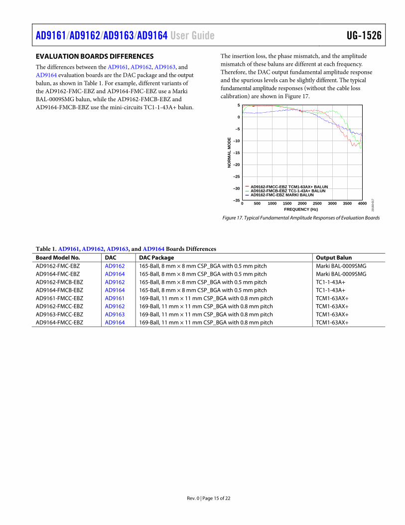
EVALUATION BOARDS DIFFERENCES The differences between the AD9161, AD9162, AD9163, and AD9164 evaluation boards are the DAC package and the output balun, as shown in Table 1. For example, different variants of the AD9162-FMC-EBZ and AD9164-FMC-EBZ use a Marki BAL-0009SMG balun, while the AD9162-FMCB-EBZ and AD9164-FMCB-EBZ use the mini-circuits TC1-1-43A+ balun.
The insertion loss, the phase mismatch, and the amplitude mismatch of these baluns are different at each frequency. Therefore, the DAC output fundamental amplitude response and the spurious levels can be slightly different. The typical fundamental amplitude responses (without the cable loss calibration) are shown in Figure 17.
NORM
AL
MO
DE
5
0
–5
–10
–15
–20
–30
–25
–350 500 1000 1500 2000
FREQUENCY (Hz)2500 3000 3500 4000
2016
0-01
7
AD9162-FMCC-EBZ TCM1-63AX+ BALUNAD9162-FMCB-EBZ TC1-1-43A+ BALUNAD9162-FMC-EBZ MARKI BALUN
Figure 17. Typical Fundamental Amplitude Responses of Evaluation Boards
Table 1. AD9161, AD9162, AD9163, and AD9164 Boards Differences Board Model No. DAC DAC Package Output Balun AD9162-FMC-EBZ AD9162 165-Ball, 8 mm × 8 mm CSP_BGA with 0.5 mm pitch Marki BAL-0009SMG AD9164-FMC-EBZ AD9164 165-Ball, 8 mm × 8 mm CSP_BGA with 0.5 mm pitch Marki BAL-0009SMG AD9162-FMCB-EBZ AD9162 165-Ball, 8 mm × 8 mm CSP_BGA with 0.5 mm pitch TC1-1-43A+ AD9164-FMCB-EBZ AD9164 165-Ball, 8 mm × 8 mm CSP_BGA with 0.5 mm pitch TC1-1-43A+ AD9161-FMCC-EBZ AD9161 169-Ball, 11 mm × 11 mm CSP_BGA with 0.8 mm pitch TCM1-63AX+ AD9162-FMCC-EBZ AD9162 169-Ball, 11 mm × 11 mm CSP_BGA with 0.8 mm pitch TCM1-63AX+ AD9163-FMCC-EBZ AD9163 169-Ball, 11 mm × 11 mm CSP_BGA with 0.8 mm pitch TCM1-63AX+ AD9164-FMCC-EBZ AD9164 169-Ball, 11 mm × 11 mm CSP_BGA with 0.8 mm pitch TCM1-63AX+
UG-1526 AD9161/AD9162/AD9163/AD9164 User Guide
Rev. 0 | Page 16 of 22
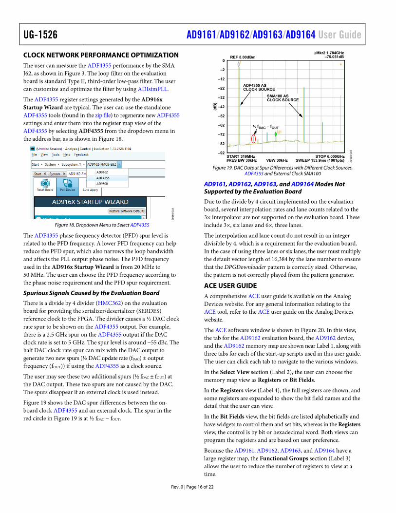
CLOCK NETWORK PERFORMANCE OPTIMIZATION The user can measure the ADF4355 performance by the SMA J62, as shown in Figure 3. The loop filter on the evaluation board is standard Type II, third-order low-pass filter. The user can customize and optimize the filter by using ADIsimPLL.
The ADF4355 register settings generated by the AD916x Startup Wizard are typical. The user can use the standalone ADF4355 tools (found in the zip file) to regenerate new ADF4355 settings and enter them into the register map view of the ADF4355 by selecting ADF4355 from the dropdown menu in the address bar, as is shown in Figure 18.
2016
0-01
8
Figure 18. Dropdown Menu to Select ADF4355
The ADF4355 phase frequency detector (PFD) spur level is related to the PFD frequency. A lower PFD frequency can help reduce the PFD spur, which also narrows the loop bandwidth and affects the PLL output phase noise. The PFD frequency used in the AD916x Startup Wizard is from 20 MHz to 50 MHz. The user can choose the PFD frequency according to the phase noise requirement and the PFD spur requirement.
Spurious Signals Caused by the Evaluation Board
There is a divide by 4 divider (HMC362) on the evaluation board for providing the serializer/deserializer (SERDES) reference clock to the FPGA. The divider causes a ½ DAC clock rate spur to be shown on the ADF4355 output. For example, there is a 2.5 GHz spur on the ADF4355 output if the DAC clock rate is set to 5 GHz. The spur level is around −55 dBc. The half DAC clock rate spur can mix with the DAC output to generate two new spurs (½ DAC update rate (fDAC) ± output frequency (fOUT)) if using the ADF4355 as a clock source.
The user may see these two additional spurs (½ fDAC ± fOUT) at the DAC output. These two spurs are not caused by the DAC. The spurs disappear if an external clock is used instead.
Figure 19 shows the DAC spur differences between the on-board clock ADF4355 and an external clock. The spur in the red circle in Figure 19 is at ½ fDAC − fOUT.
ADF4355 ASCLOCK SOURCE
SMA100 ASCLOCK SOURCE
½ fDAC – fOUT
0
∆Mkr2 1.784GHz–75.051dBREF 8.00dBm
–2
–12
(dB
)
–22
–32
–42
–52
–62
–72
–82
–92START 319MHz#RES BW 30kHz VBW 30kHz
STOP 6.000GHzSWEEP 153.9ms (1001pts) 20
160-
019
Figure 19. DAC Output Spur Differences with Different Clock Sources,
ADF4355 and External Clock SMA100
AD9161, AD9162, AD9163, and AD9164 Modes Not Supported by the Evaluation Board
Due to the divide by 4 circuit implemented on the evaluation board, several interpolation rates and lane counts related to the 3× interpolator are not supported on the evaluation board. These include 3×, six lanes and 6×, three lanes.
The interpolation and lane count do not result in an integer divisible by 4, which is a requirement for the evaluation board. In the case of using three lanes or six lanes, the user must multiply the default vector length of 16,384 by the lane number to ensure that the DPGDownloader pattern is correctly sized. Otherwise, the pattern is not correctly played from the pattern generator.
ACE USER GUIDE A comprehensive ACE user guide is available on the Analog Devices website. For any general information relating to the ACE tool, refer to the ACE user guide on the Analog Devices website.
The ACE software window is shown in Figure 20. In this view, the tab for the AD9162 evaluation board, the AD9162 device, and the AD9162 memory map are shown near Label 1, along with three tabs for each of the start-up scripts used in this user guide. The user can click each tab to navigate to the various windows.
In the Select View section (Label 2), the user can choose the memory map view as Registers or Bit Fields.
In the Registers view (Label 4), the full registers are shown, and some registers are expanded to show the bit field names and the detail that the user can view.
In the Bit Fields view, the bit fields are listed alphabetically and have widgets to control them and set bits, whereas in the Registers view, the control is by bit or hexadecimal word. Both views can program the registers and are based on user preference.
Because the AD9161, AD9162, AD9163, and AD9164 have a large register map, the Functional Groups section (Label 3) allows the user to reduce the number of registers to view at a time.

AD9161/AD9162/AD9163/AD9164 User Guide UG-1526
Rev. 0 | Page 17 of 22
For example, Figure 20 shows the JESD_Control functional group, which is useful because the four registers required to configure the JESD204B link are all in that group.
By selecting this group and expanding the registers, the user can quickly find the registers and update their values. Click the Apply Selected or Apply Changes button above Label 2 after a register is changed to commit the change and program it to the device.
The user can use the Bit Fields view in conjunction with functional groups. In Figure 20 the bit fields associated with the selected functional group is shown.
The Macro Tools section (Label 5) is above the list of macros that are currently open in the session. The user can click the name of the desired macro to make it active in the window. Click the Play button (right pointing triangle) to play the selected macro.
The user can use the Search field (Label 6) to find a bit field.
The user can enable the Macro Tools window from the View menu in the main ACE window and checking Macro Tools. A separate window appears on the right side, as shown in Figure 20.
1
2
3
4 5
6
2016
0-02
0
Figure 20. JESD_Control Functional Group View of the AD9161, AD9162, AD9163, and AD9164 in ACE

UG-1526 AD9161/AD9162/AD9163/AD9164 User Guide
Rev. 0 | Page 18 of 22
JESD204B LANE MAPPING OF THE EVALUATION BOARD The ADS7-V2EBZ is based on a Xilinx® Virtex7 FPGA device. The user can configure another Xilinx Virtex7-based evaluation board to drive the AD9161 series evaluation board. The JESD204B parameters are available in the AD9161, AD9162, AD9163, and AD9164 data sheets.
The physical lanes on the FMC connector are not necessarily connected to the same lanes on the AD9161, AD9162, AD9163, and AD9164. The AD9161, AD9162, AD9163, and AD9164 have a cross bar switch on the JESD204B link. However, in the case of the ADS7-V2EBZ, AD9161, AD9162, AD9163, and AD9164, mapping is done using the cross bar in the Xilinx JESD204B transmitter.
The following list is the mapping between the FMC lanes and the AD9161, AD9162, AD9163, and AD9164 lanes on the evaluation board. The mapping to the Xilinx JESD204B intellectual property (IP) is also provided in the following list for reference.
• Physical Lane 0 on the FMC connector (DP0_C2M) is also Lane 0 on the AD9161, AD9162, AD9163, and AD9164 (Lane 0 the Xilinx JESD204B IP)
• Physical Lane 1 on the FMC connector (DP1_C2M) is also Lane 1 on the AD9161, AD9162, AD9163, and AD9164 (Lane 1 out of the Xilinx JESD204B IP)
• Physical Lane 2 on the FMC connector (DP2_C2M) is also Lane 2 on the AD9161, AD9162, AD9163, and AD9164 (Lane 2 out of the Xilinx JESD204B IP)
• Physical Lane 3 on the FMC connector (DP3_C2M) is also Lane 3 on the AD9161, AD9162, AD9163, and AD9164 (Lane 3 out of the Xilinx JESD204B IP)
• Physical Lane 4 on the FMC connector (DP4_C2M) is Lane 5 on the AD9161, AD9162, AD9163, and AD9164 (Lane 5 out of the Xilinx JESD204B IP)
• Physical Lane 5 on the FMC connector (DP5_C2M) is Lane 7 on the AD9161, AD9162, AD9163, and AD9164 (Lane 7 out of the Xilinx JESD204B IP)
• Physical Lane 6 on the FMC connector (DP6_C2M) is also Lane 6 on the AD9161, AD9162, AD9163, and AD9164 (Lane 6 out of the Xilinx JESD204B IP)
• Physical Lane 7 on the FMC connector (DP7_C2M) is Lane 4 on the AD9161, AD9162, AD9163, and AD9164 (Lane 4 out of the Xilinx JESD204B IP)
There is also input data pin polarity (positive/negative (P/N)) inversion between the transmitter and receiver on the evaluation board to ease layout. The polarity can easily be inverted in the Xilinx physical layer by inverting Physical Lane 4 to Lane 7 (DP4_C2M to DP7_C2M) on the FMC connector (P/N swapped).
When the JESD204B is running, the following are a few debug ideas. Monitor the sync lane.
• If the sync lane stays low, the JESD204B reference frequency needs to be adjusted.
• Sync lane toggles: P/N lanes needs to be adjusted. Otherwise, with inverted polarity, K character passes, but initial lane alignment sequence (ILAS) does not pass, creating sync signal toggling.
• Sync stays high, but output spectrum is not valid. Transport or mapping of lane is wrong.
Note that in 3-lane or 6-lane mode, single-tone record length is multiples of 3. Otherwise, the output spectrum is not correct. An example is shown in Figure 21.
2016
0-02
1
Figure 21. Record Length in 3-Lane/6-Lane Mode

AD9161/AD9162/AD9163/AD9164 User Guide UG-1526
Rev. 0 | Page 19 of 22
TROUBLESHOOTING Debugging the Evaluation Board Using On-Board LEDs
There are five LEDs on the evaluation board, which are the 12 V power supply LED, the ADF4355 reference clock LED, the USB connected LED, the AD9161, AD9162, AD9163, and AD9164 PWR_BAD LED, and the AD9161, AD9162, AD9163, and AD9164 DAC interruption LED.
These LEDs are shown in Figure 22. If the evaluation board is properly configured, the 12 V power LED, ADF4355 reference clock LED, and USB connected LED are lit. The PWR_BAD LED is lit when the AD9161, AD9162, AD9163, and AD9164 are not powered properly.
XCR1: USB CONNECTION LED
DS2: 12V POWER SUPPLY LED 2016
0-02
2
CR5: DAC INTERRUPT REQUEST
J61: ADF4355REF CLOCK
DS1: POWER_BAD ERROR
Figure 22. Five LEDs on the Evaluation Board

UG-1526 AD9161/AD9162/AD9163/AD9164 User Guide
Rev. 0 | Page 20 of 22
DPGDownloader Does Not Recognize the Evaluation Board
The evaluation board can be run with or without an ADS7-V2EBZ. To download a valid image to the FPGA, open the DPGDownloader with the USB cable connected to the PC and the ADS7-V2EBZ. The DPGDownloader recognizes the ADS7-V2EBZ and reads the board ID of the evaluation board (if it is connected) through the FMC connector. The DPGDownloader then downloads a valid image and powers on the evaluation board automatically.
There may be cases where the DPGDownloader does not recognize the evaluation board. If this occurs, open the DPGDownloader and unplug then replug the USB cable. If DPGDownloader still does not recognize the evaluation board, there is a chance that the firmware of the board is not updated and the evaluation board must be reprogrammed with new firmware. Contact a local Analog Devices sales person or distributor to arrange for this reprogramming to be done.
DPGDownloader Does Not Recognize an ADS7-V2EBZ
The DPGDownloader software may not recognize the ADS7-V2EBZ board. Unplug the USB cable from the ADS7-V2EBZ and replug it into the ADS7-V2EBZ. The DPGDownloader software recognizes the ADS7-V2EBZ.
If the DPGDownloader recognizes the ADS7-V2EBZ, the DPGDownloader downloads a generic image to the FPGA. If the evaluation board is plugged into the ADS7-V2EBZ with the FMC connector prior to the USB cable being plugged in to the ADS7-V2EBZ, the DPGDownloader software recognizes the ADS7-V2EBZ, reads the evaluation board identifier through the FMC connector, and downloads an AD9161, AD9162, AD9163, or AD9164 image to the evaluation board.
JESD204B Link Is Not Established
The start-up sequences referenced in this user guide are tested on the evaluation board and known to work. There may be cases when the JESD204B link is not established. This section provides debug solutions for that situation. However, this section does not cover every possible scenario. When in doubt, power cycle all hardware, reopen the ACE software, reopen the
DPGDownloader software, and follow one of the quick start routines mentioned in this user guide. Notice the differences from the routines in this user guide as compared to the setup and make the changes step by step, and observe where the issue is created.
The following are some debugging suggestions for when the SERDES link is not established:
Check to ensure that the DPGDownloader has a pattern selected and the pattern is playing, for example, sending data to the evaluation board. The link is not established if there is no data being sent to the DAC.
Check that Subclass 0, the default subclass, is selected. The user guide examples all use Subclass 0.
Ensure that the JESD204B Line Rate reported by the DPGDownloader is exactly reflecting the same line rate that ACE reports.
If the evaluation board was previously configured for either NCO mode or JESD204B mode, reset the board by performing a power cycle, by using the Reset Board button in the evaluation board view window (see Figure 6) of ACE, or by using the Reset Chip button in the device view window (see Figure 8).
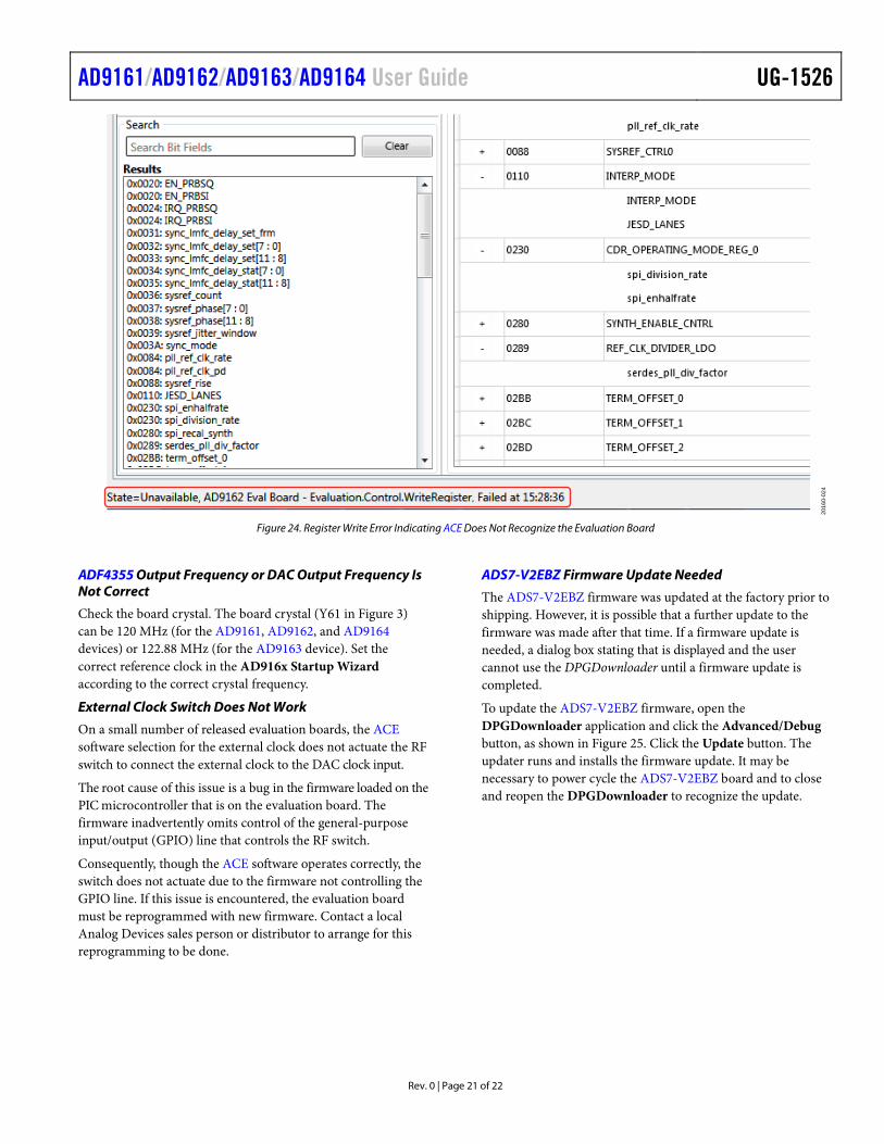
ACE Does Not Recognize the Evaluation Board
One of two possible errors can be generated, as shown in Figure 23 and Figure 24. Both of these error messages indicate that the ACE software does not recognize the evaluation board.
These errors can occur if the ACE software is started before powering up and connecting the evaluation board to the PC, or if the evaluation board is power cycled and ACE is not restarted.
The most basic remedy for this issue is to close ACE and reopen it (restart). As long as the evaluation board is powered up and connected to the PC, ACE recognizes the evaluation board and the scripts and register writes work again.
2016
0-02
3
Figure 23. Script Error Window Indicating ACE Does Not Recognize the Evaluation Board
AD9161/AD9162/AD9163/AD9164 User Guide UG-1526
Rev. 0 | Page 21 of 22
2016
0-02
4
Figure 24. Register Write Error Indicating ACE Does Not Recognize the Evaluation Board
ADF4355 Output Frequency or DAC Output Frequency Is Not Correct
Check the board crystal. The board crystal (Y61 in Figure 3) can be 120 MHz (for the AD9161, AD9162, and AD9164 devices) or 122.88 MHz (for the AD9163 device). Set the correct reference clock in the AD916x Startup Wizard according to the correct crystal frequency.
External Clock Switch Does Not Work
On a small number of released evaluation boards, the ACE software selection for the external clock does not actuate the RF switch to connect the external clock to the DAC clock input.
The root cause of this issue is a bug in the firmware loaded on the PIC microcontroller that is on the evaluation board. The firmware inadvertently omits control of the general-purpose input/output (GPIO) line that controls the RF switch.
Consequently, though the ACE software operates correctly, the switch does not actuate due to the firmware not controlling the GPIO line. If this issue is encountered, the evaluation board must be reprogrammed with new firmware. Contact a local Analog Devices sales person or distributor to arrange for this reprogramming to be done.
ADS7-V2EBZ Firmware Update Needed
The ADS7-V2EBZ firmware was updated at the factory prior to shipping. However, it is possible that a further update to the firmware was made after that time. If a firmware update is needed, a dialog box stating that is displayed and the user cannot use the DPGDownloader until a firmware update is completed.
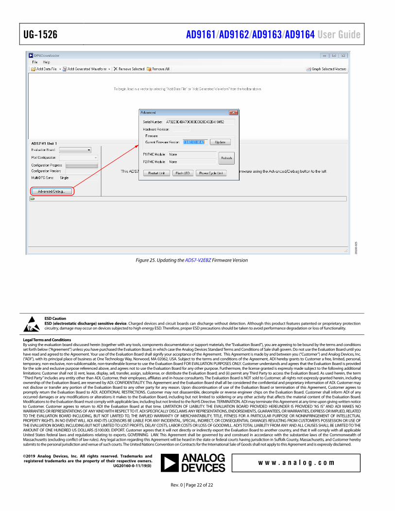
To update the ADS7-V2EBZ firmware, open the DPGDownloader application and click the Advanced/Debug button, as shown in Figure 25. Click the Update button. The updater runs and installs the firmware update. It may be necessary to power cycle the ADS7-V2EBZ board and to close and reopen the DPGDownloader to recognize the update.
UG-1526 AD9161/AD9162/AD9163/AD9164 User Guide
Rev. 0 | Page 22 of 22
2016
0-02
5
Figure 25. Updating the ADS7-V2EBZ Firmware Version
ESD Caution ESD (electrostatic discharge) sensitive device. Charged devices and circuit boards can discharge without detection. Although this product features patented or proprietary protection circuitry, damage may occur on devices subjected to high energy ESD. Therefore, proper ESD precautions should be taken to avoid performance degradation or loss of functionality.
Legal Terms and Conditions By using the evaluation board discussed herein (together with any tools, components documentation or support materials, the “Evaluation Board”), you are agreeing to be bound by the terms and conditions set forth below (“Agreement”) unless you have purchased the Evaluation Board, in which case the Analog Devices Standard Terms and Conditions of Sale shall govern. Do not use the Evaluation Board until you have read and agreed to the Agreement. Your use of the Evaluation Board shall signify your acceptance of the Agreement. This Agreement is made by and between you (“Customer”) and Analog Devices, Inc. (“ADI”), with its principal place of business at One Technology Way, Norwood, MA 02062, USA. Subject to the terms and conditions of the Agreement, ADI hereby grants to Customer a free, limited, personal, temporary, non-exclusive, non-sublicensable, non-transferable license to use the Evaluation Board FOR EVALUATION PURPOSES ONLY. Customer understands and agrees that the Evaluation Board is provided for the sole and exclusive purpose referenced above, and agrees not to use the Evaluation Board for any other purpose. Furthermore, the license granted is expressly made subject to the following additional limitations: Customer shall not (i) rent, lease, display, sell, transfer, assign, sublicense, or distribute the Evaluation Board; and (ii) permit any Third Party to access the Evaluation Board. As used herein, the term “Third Party” includes any entity other than ADI, Customer, their employees, affiliates and in-house consultants. The Evaluation Board is NOT sold to Customer; all rights not expressly granted herein, including ownership of the Evaluation Board, are reserved by ADI. CONFIDENTIALITY. This Agreement and the Evaluation Board shall all be considered the confidential and proprietary information of ADI. Customer may not disclose or transfer any portion of the Evaluation Board to any other party for any reason. Upon discontinuation of use of the Evaluation Board or termination of this Agreement, Customer agrees to promptly return the Evaluation Board to ADI. ADDITIONAL RESTRICTIONS. Customer may not disassemble, decompile or reverse engineer chips on the Evaluation Board. Customer shall inform ADI of any occurred damages or any modifications or alterations it makes to the Evaluation Board, including but not limited to soldering or any other activity that affects the material content of the Evaluation Board. Modifications to the Evaluation Board must comply with applicable law, including but not limited to the RoHS Directive. TERMINATION. ADI may terminate this Agreement at any time upon giving written notice to Customer. Customer agrees to return to ADI the Evaluation Board at that time. LIMITATION OF LIABILITY. THE EVALUATION BOARD PROVIDED HEREUNDER IS PROVIDED “AS IS” AND ADI MAKES NO WARRANTIES OR REPRESENTATIONS OF ANY KIND WITH RESPECT TO IT. ADI SPECIFICALLY DISCLAIMS ANY REPRESENTATIONS, ENDORSEMENTS, GUARANTEES, OR WARRANTIES, EXPRESS OR IMPLIED, RELATED TO THE EVALUATION BOARD INCLUDING, BUT NOT LIMITED TO, THE IMPLIED WARRANTY OF MERCHANTABILITY, TITLE, FITNESS FOR A PARTICULAR PURPOSE OR NONINFRINGEMENT OF INTELLECTUAL PROPERTY RIGHTS. IN NO EVENT WILL ADI AND ITS LICENSORS BE LIABLE FOR ANY INCIDENTAL, SPECIAL, INDIRECT, OR CONSEQUENTIAL DAMAGES RESULTING FROM CUSTOMER’S POSSESSION OR USE OF THE EVALUATION BOARD, INCLUDING BUT NOT LIMITED TO LOST PROFITS, DELAY COSTS, LABOR COSTS OR LOSS OF GOODWILL. ADI’S TOTAL LIABILITY FROM ANY AND ALL CAUSES SHALL BE LIMITED TO THE AMOUNT OF ONE HUNDRED US DOLLARS ($100.00). EXPORT. Customer agrees that it will not directly or indirectly export the Evaluation Board to another country, and that it will comply with all applicable United States federal laws and regulations relating to exports. GOVERNING LAW. This Agreement shall be governed by and construed in accordance with the substantive laws of the Commonwealth of Massachusetts (excluding conflict of law rules). Any legal action regarding this Agreement will be heard in the state or federal courts having jurisdiction in Suffolk County, Massachusetts, and Customer hereby submits to the personal jurisdiction and venue of such courts. The United Nations Convention on Contracts for the International Sale of Goods shall not apply to this Agreement and is expressly disclaimed.
©2019 Analog Devices, Inc. All rights reserved. Trademarks and registered trademarks are the property of their respective owners. UG20160-0-11/19(0)