AD568 12-Bit Ultrahigh Speed Monolithic D/A Converter · FUNCTIONAL BLOCK DIAGRAM REV. A...
14
FUNCTIONAL BLOCK DIAGRAM REV. A Information furnished by Analog Devices is believed to be accurate and reliable. However, no responsibility is assumed by Analog Devices for its use, nor for any infringements of patents or other rights of third parties which may result from its use. No license is granted by implication or otherwise under any patent or patent rights of Analog Devices. a 12-Bit Ultrahigh Speed Monolithic D/A Converter AD568 FEATURES Ultrahigh Speed: Current Settling to 1 LSB in 35 ns High Stability Buried Zener Reference on Chip Monotonicity Guaranteed Over Temperature 10.24 mA Full-Scale Output Suitable for Video Applications Integral and Differential Linearity Guaranteed Over Temperature 0.3" “Skinny DIP” Packaging Variable Threshold Allows TTL and CMOS Interface MIL-STD-883 Compliant Versions Available PRODUCT DESCRIPTION The AD568 is an ultrahigh-speed, 12-bit digital-to-analog con- verter (DAC) settling to 0.025% in 35 ns. The monolithic de- vice is fabricated using Analog Devices’ Complementary Bipolar (CB) Process. This is a proprietary process featuring high-speed NPN and PNP devices on the same chip without the use of di- electric isolation or multichip hybrid techniques. The high speed of the AD568 is maintained by keeping impedance levels low enough to minimize the effects of parasitic circuit capacitances. The DAC consists of 16 current sources configured to deliver a 10.24 mA full-scale current. Multiple matched current sources and thin-film ladder techniques are combined to produce bit weighting. The DAC’s output is a 10.24 mA full scale (FS) for current output applications or a 1.024 V FS unbuffered voltage output. Additionally, a 10.24 V FS buffered output may be gen- erated using an onboard 1 kΩ span resistor with an external op amp. Bipolar ranges are accomplished by pin strapping. Laser wafer trimming insures full 12-bit linearity. All grades of the AD568 are guaranteed monotonic over their full operating temperature range. Furthermore, the output resistance of the DAC is trimmed to 100 Ω ± 1.0%. The gain temperature coeffi- cient of the voltage output is 30 ppm/°C max (K). The AD568 is available in three performance grades. The AD568JQ and KQ are available in 24-pin cerdip (0.3") packages and are specified for operation from 0°C to +70°C. The AD568SQ features operation from –55°C to +125°C and is also packaged in the hermetic 0.3" cerdip. One Technology Way, P.O. Box 9106, Norwood, MA 02062-9106, U.S.A. Tel: 617/329-4700 Fax: 617/326-8703 PRODUCT HIGHLIGHTS 1. The ultrafast settling time of the AD568 allows leading edge performance in waveform generation, graphics display and high speed A/D conversion applications. 2. Pin strapping provides a variety of voltage and current output ranges for application versatility. Tight control of the abso- lute output current reduces trim requirements in externally- scaled applications. 3. Matched on-chip resistors can be used for precision scaling in high speed A/D conversion circuits. 4. The digital inputs are compatible with TTL and +5 V CMOS logic families. 5. Skinny DIP (0.3") packaging minimizes board space require- ments and eases layout considerations. 6. The AD568 is available in versions compliant with MIL- STD-883. Refer to the Analog Devices Military Products Databook or current AD568/883B data sheet for detailed specifications.
Transcript of AD568 12-Bit Ultrahigh Speed Monolithic D/A Converter · FUNCTIONAL BLOCK DIAGRAM REV. A...

FUNCTIONAL BLOCK DIAGRAM
REV. A
Information furnished by Analog Devices is believed to be accurate andreliable. However, no responsibility is assumed by Analog Devices for itsuse, nor for any infringements of patents or other rights of third partieswhich may result from its use. No license is granted by implication orotherwise under any patent or patent rights of Analog Devices.
a 12-Bit Ultrahigh SpeedMonolithic D/A Converter
AD568FEATURES
Ultrahigh Speed: Current Settling to 1 LSB in 35 ns
High Stability Buried Zener Reference on Chip
Monotonicity Guaranteed Over Temperature
10.24 mA Full-Scale Output Suitable for Video
Applications
Integral and Differential Linearity Guaranteed Over
Temperature
0.3" “Skinny DIP” Packaging
Variable Threshold Allows TTL and CMOS
Interface
MIL-STD-883 Compliant Versions Available
PRODUCT DESCRIPTIONThe AD568 is an ultrahigh-speed, 12-bit digital-to-analog con-verter (DAC) settling to 0.025% in 35 ns. The monolithic de-vice is fabricated using Analog Devices’ Complementary Bipolar(CB) Process. This is a proprietary process featuring high-speedNPN and PNP devices on the same chip without the use of di-electric isolation or multichip hybrid techniques. The high speedof the AD568 is maintained by keeping impedance levels lowenough to minimize the effects of parasitic circuit capacitances.
The DAC consists of 16 current sources configured to deliver a10.24 mA full-scale current. Multiple matched current sourcesand thin-film ladder techniques are combined to produce bitweighting. The DAC’s output is a 10.24 mA full scale (FS) forcurrent output applications or a 1.024 V FS unbuffered voltageoutput. Additionally, a 10.24 V FS buffered output may be gen-erated using an onboard 1 kΩ span resistor with an external opamp. Bipolar ranges are accomplished by pin strapping.
Laser wafer trimming insures full 12-bit linearity. All grades ofthe AD568 are guaranteed monotonic over their full operatingtemperature range. Furthermore, the output resistance of theDAC is trimmed to 100 Ω ± 1.0%. The gain temperature coeffi-cient of the voltage output is 30 ppm/°C max (K).
The AD568 is available in three performance grades. TheAD568JQ and KQ are available in 24-pin cerdip (0.3") packagesand are specified for operation from 0°C to +70°C. TheAD568SQ features operation from –55°C to +125°C and is alsopackaged in the hermetic 0.3" cerdip.
One Technology Way, P.O. Box 9106, Norwood, MA 02062-9106, U.S.A.
Tel: 617/329-4700 Fax: 617/326-8703
PRODUCT HIGHLIGHTS1. The ultrafast settling time of the AD568 allows leading edge
performance in waveform generation, graphics display andhigh speed A/D conversion applications.
2. Pin strapping provides a variety of voltage and current outputranges for application versatility. Tight control of the abso-lute output current reduces trim requirements in externally-scaled applications.
3. Matched on-chip resistors can be used for precision scaling inhigh speed A/D conversion circuits.
4. The digital inputs are compatible with TTL and +5 VCMOS logic families.
5. Skinny DIP (0.3") packaging minimizes board space require-ments and eases layout considerations.
6. The AD568 is available in versions compliant with MIL-STD-883. Refer to the Analog Devices Military ProductsDatabook or current AD568/883B data sheet for detailedspecifications.

Model AD568J AD568K AD568SMin Typ Max Min Typ Max Min Typ Max Units
RESOLUTION 12 12 12 Bits
ACCURACY1
Linearity –1/2 +1/2 –1/4 +1/4 –1/2 +1/2 LSBTMIN to TMAX –3/4 +3/4 –1/2 +1/2 –3/4 +3/4 LSB
Differential Nonlinearity –1 +1 –1/2 +1/2 –1 +1 LSBTMIN to TMAX –1 +1 –1 + 1 –1 –1 LSB
Monotonicity GUARANTEED OVER RATED SPECIFICATION TEMPERATURE RANGEUnipolar Offset –0.2 +0.2 * * * * % of FSRBipolar Offset –1.0 +1.0 * * * * % of FSRBipolar Zero –0.2 +0.2 * * * * % of FSRGain Error –1.0 +1.0 * * * * % of FSR
TEMPERATURE COEFFICIENTS2
Unipolar Offset –5 +5 –3 +3 –5 +5 ppm of FSR/°CBipolar Offset –30 +30 –20 +20 –30 +30 ppm of FSR/°CBipolar Zero –15 +15 • • • • ppm of FSR/°CGain Drift –50 +50 –30 +30 –50 +50 ppm of FSR/°CGain Drift (IOUT) –150 +150 * * * * ppm of FSR/°C
DATA INPUTSLogic Levels (TMIN to TMAX)
VIH 2.0 7.0 * * * * VVIL 0.0 0.8 * * * * V
Logic Currents (TMIN to TMAX)IIH –10 0 +10 * * * * * * µAIIL –0.5 –60 –100 * * * * –100 –200 µAVTH Pin Voltage 1.4 * * V
CODING BINARY, OFFSET BINARY
CURRENT OUTPUT RANGES 0 to 10.24, ±5.12 mA
VOLTAGE OUTPUT RANGES 0 to 1.024, ±0.512 V
COMPLIANCE VOLTAGE –2 +1.2 * * * * V
OUTPUT RESISTANCEExclusive of RL 160 200 240 * * ΩInclusive of RL 99 100 101 * * Ω
SETTLING TIMECurrent to
± 0.025% 35 * * ns to 0.025% of FSR± 0.1% 23 * * ns to 0.1% of FSR
Voltage50 Ω Load3, 0.512 V p-p,
to 0.025% 37 * * ns to 0.025% of FSRto 0.1% 25 * * ns to 0.1% of FSRto 1% 18 * * ns to 1% of FSR
75 Ω Load3, 0.768 V p-p,to 0.025% 40 * * ns to 0.025% of FSRto 0.1% 25 * * ns to 0.1% of FSRto 1% 20 * * ns to 1% of FSR
100 Ω (Internal RL)3, 1.024 V p-p,to 0.025% 50 * * ns to 0.025% of FSRto 0.1% 38 * * ns to 0.1% of FSRto 1% 24 * * ns to 1% of FSR
Glitch Impulse4 350 * * pV-secPeak Amplitude 15 * * % of FSR
FULL-SCALE TRANSlTlON5
10% to 90% Rise Time 11 * * ns90% to 10% Fall Time 11 * * ns
POWER REQUIREMENTS+13.5 V to +16.5 V 27 32 * * * * mA–13.5 V to –16.5 V –7 –8 * * * * mAPower Dissipation 525 625 * * * * mWPSRR 0.05 * * % of FSR/V
TEMPERATURE RANGE Rated Specification2 0 +70 0 +70 –55 +125 °C
Storage –65 +150 * * * * °C
NOTES*Same as AD568J.1Measured in IOUT mode.2Measured in VOUT mode, unless otherwise specified. See text for further information.3Total Resistance. Refer to Figure 3,4At the major carry, driven by HCMOS logic. See text for further explanation.5Measured in VOUT mode.
Specifications shown in boldface are tested on all production units at final electrical test.Specifications subject to change without notice.
REV. A–2–
(@ = +258C, VCC, VEE = 615 V unless otherwise noted)AD568–SPECIFICATIONS
AD568
REV. A –3–
ORDERING GUIDE
Linearity VoltageTemperature Error Max Gain T.C.
Modell Package Option2 Range 8C @ 258C Max ppm/8C
AD568JQ 24-Lead Cerdip (Q-24) 0 to +70 ±1/2 ±50AD568KQ 24-Lead Cerdip (Q-24) 0 to +70 ±1/4 ±30AD568SQ 24-Lead Cerdip (Q-24) –55 to +125 ±1/2 ±50NOTES1For details on grade and package offerings screened in accordance with MIL-STD-883, refer to the Analog Devices Military Products Databook or current AD568/883B data sheet.2Q = Cerdip.
DefinitionsLINEARITY ERROR (also called INTEGRAL NONLINEAR-ITY OR INL): Analog Devices defines linearity error as themaximum deviation of the actual analog output from the idealoutput (a straight line drawn from 0 to FS) for any bit combina-tion expressed in multiples of 1 LSB. The AD568 is lasertrimmed to 1/4 LSB (0.006% of FS) maximum linearity error at+25°C for the K version and 1/2 LSB for the J and S versions.
DIFFERENTIAL LINEARITY ERROR (also called DIFFER-ENTIAL NONLINEARITY or DNL): DNL is the measure ofthe variation in analog value, normalized to full scale, associatedwith a 1 LSB change in digital input code. Monotonic behavior
WARNING!
ESD SENSITIVE DEVICE
CAUTIONESD (electrostatic discharge) sensitive device. Electrostatic charges as high as 4000 V readilyaccumulate on the human body and test equipment and can discharge without detection.Although the AD568 features proprietary ESD protection circuitry, permanent damage mayoccur on devices subjected to high energy electrostatic discharges. Therefore, proper ESDprecautions are recommended to avoid performance degradation or loss of functionality.
requires that the differential linearity error not exceed 1 LSB inthe negative direction.
MONOTONICITY: A DAC is said to be monotonic if the out-put either increases or remains constant as the digital inputincreases.
UNIPOLAR OFFSET ERROR: The deviation of the analogoutput from the ideal (0 V or 0 mA) when the inputs are set toall 0s is called unipolar offset error.
BIPOLAR OFFSET ERROR: The deviation of the analog out-put from the ideal (negative half-scale) when the inputs are setto all 0s is called bipolar offset error.
18
6789101112 12345
19
20
23
24
13
14
17
2X 4X
MSBLSB
PNPCURRENTSOURCES
1.4VBAND-GAPREF
THRESHOLDCONTROL
THRESHOLDCOMMON
LADDERCOMMON
PNPSWITCHES
DIFFUSED R-2R LADDER(10 - 20Ω)
THIN-FILM R-2R LADDER(100 - 200Ω)
BIPOLARCURRENT
GENERATOR
BURIEDZENER
REFERENCE
21
22
200Ω
ANALOGCOMMON
VCC
IOUT
REFERENCECOMMON
1kΩ
15
16
LOAD RESISTOR(RL)
BIPOLAROFFSET (IBPO)10V SPANRESISTOR
10V SPANRESISTOR
IOUT
IOUT
AD568
VEE
Figure 1. Functional Block Diagram
ABSOLUTE MAXIMUM RATINGS1
VCC to REFCOM . . . . . . . . . . . . . . . . . . . . . . . . 0 V to +18 VVEE to REFCOM . . . . . . . . . . . . . . . . . . . . . . . . . 0 V to –18 VREFCOM to LCOM . . . . . . . . . . . . . . . . . +100 mV to –10 VACOM to LCOM . . . . . . . . . . . . . . . . . . . . . . . . . . . ±100 mVTHCOM to LCOM . . . . . . . . . . . . . . . . . . . . . . . . . . ±500 mVSPANs to LCOM . . . . . . . . . . . . . . . . . . . . . . . . . . . . . ±12 VIBPO to LCOM . . . . . . . . . . . . . . . . . . . . . . . . . . . . . . . . . ±5 VIOUT to LCOM . . . . . . . . . . . . . . . . . . . . . . . . . . . –5 V to VTH
Digital Inputs to THCOM . . . . . . . . . . . . . –500 mV to +7.0 VVoltage Across Span Resistor . . . . . . . . . . . . . . . . . . . . . . 12 VVTH to THCOM . . . . . . . . . . . . . . . . . . . . . . –0.7 V to +1.4 VLogic Threshold Control Input Current . . . . . . . . . . . . . 5 mA
Power Dissipation . . . . . . . . . . . . . . . . . . . . . . . . . . . 100 mWStorage Temperature Range
Q (Cerdip) Package . . . . . . . . . . . . . . . . . –65°C to +150°CJunction Temperature . . . . . . . . . . . . . . . . . . . . . . . . . . 175°CThermal Resistance
θJA . . . . . . . . . . . . . . . . . . . . . . . . . . . . . . . . . . . . . . 75°C/WθJC . . . . . . . . . . . . . . . . . . . . . . . . . . . . . . . . . . . . . . 25°C/W
1Stresses above those listed under “Absolute Maximum Ratings” may causepermanent damage to the device. This is a stress rating only and functionaloperation of the device at these or any other conditions above those indicated in theoperational section of this specification is not implied. Exposure to absolutemaximum rating conditions for extended periods may affect device reliability.
PIN CONFIGURATION

AD568
REV. A–4–
their glitch impulse. It is specified as the net area of the glitch innV-sec or pA-sec.
COMPLIANCE VOLTAGE: The range of allowable voltage atthe output of a current-output DAC which will not degrade theaccuracy of the output current.
SETTLING TIME: The time required for the output to reachand remain within a specified error band about its final value,measured from the digital input transition.
TIME – ns
0.8
0 25050
OU
TP
UT
– V
OL
TS
100 150 200
0.6
0.4
Figure 2. Glitch Impulse
Connecting the AD568UNBUFFERED VOLTAGE OUTPUT
Unipolar ConfigurationFigure 3 shows the AD568 configured to provide a unipolar 0 to+1.024 V output range. In this mode, the bipolar offset termi-nal, Pin 21, should be grounded if not used for offset trimming.
The nominal output impedance of the AD568 with Pin 19grounded has been trimmed to 100 Ω, ±1%. Other output im-pedances can be generated with an external resistor, REXT, be-tween Pins 19 and 20. An REXT equalling 300 Ω will yield atotal output resistance of 75 Ω, while an REXT of 100 Ω will pro-vide 50 Ω of output resistance. Note that since the full-scaleoutput current of the DAC remains 10.24 mA, changing theload impedance changes the unbuffered output voltage accord-ingly. Settling time and full-scale range characteristics for theseload impedances are provided in the specifications table.
Bipolar ConfigurationFigure 4 shows the connection scheme used to provide a bipolaroutput voltage range of 1.024 V. The bipolar offset (–0.512 V)occurs when all bits are OFF (00 . . . 00), bipolar zero (0 V) oc-curs when the MSB is ON with all other bits OFF (10 . . . 00),and full-scale minus 1 LSB (0.51175 V) is generated when allbits are ON (11 . . . 11). Figure 5 shows an optional bipolarmode with a 2.048 V range. The scale factor in this mode willnot be as accurate as the configuration shown in Figure 4, be-cause the laser-trimmed resistor RL is not used.
13
16
15
14
24
23
22
21
20
19
18
17
12
11
10
9
8
1
2
3
4
7
6
5
AD568
+15V
REFCOM
–15V
IBPO
RL
ACOM
LCOM
SPAN
SPAN
THCOM
VTH
IOUT
DIGITALINPUTS
0.2µF
0.1µF
0.1µF
0.1µF
–15V+15V
ANALOGGND PLANE
DIGITALGND PLANE DIGITAL
SUPPLYGROUND
100pF
RTH1kΩ
+5V
ANALOGOUTPUT
REXT(OPTIONAL)
FERRITE BEADSSTACKPOLE 57-1392ORAMIDON FB-43B-101OR EQUIVALENT
NC
NC
ANALOGSUPPLY GROUND
Figure 3. Unipolar Output Unbuffered 0 V to +1.024 V
13
16
15
14
24
23
22
21
20
19
18
17
12
11
10
9
8
1
2
3
4
7
6
5
AD568
+15V
REFCOM
–15V
IBPO
RL
ACOM
LCOM
SPAN
SPAN
THCOM
VTH
IOUT
DIGITALINPUTS
0.2µF
0.1µF
0.1µF
0.1µF
–15V+15V
ANALOGGND PLANE
DIGITALGND PLANE DIGITAL
SUPPLYGROUND
100pF
+5V
ANALOGOUTPUT
ANALOGSUPPLYGROUND
Figure 4. Bipolar Output Unbuffered ±0.512 V
Figure 4 also demonstrates how the internal span resistor maybe used to bias the VTH pin (Pin 13) from a 5 V supply. Thiseliminates the requirement for an external RTH in applicationsthat do not require the precision span resistor.
BIPOLAR ZERO ERROR: The deviation of the analog outputfrom the ideal half-scale output of 0 V (or 0 mA) for bipolarmode when only the MSB is on (100 . . .00) is called bipolarzero error.
GAIN ERROR: The difference between the ideal and actualoutput span of FS –1 LSB, expressed in % of FS, or LSB, whenall bits are on.
GLITCH IMPULSE: Asymmetrical switching times in a DACgive rise to undesired output transients which are quantified by
AD568
REV. A –5–
13
16
15
14
24
23
22
21
20
19
18
17
12
11
10
9
8
1
2
3
4
7
6
5
AD568
+15V
REFCOM
–15V
IBPO
RL
ACOM
LCOM
SPAN
SPAN
THCOM
VTH
IOUT
DIGITALINPUTS
0.2µF
0.1µF
0.1µF
0.1µF
–15V+15V
ANALOGGND PLANE
DIGITALGND PLANE DIGITAL
SUPPLYGROUND
100pF
RTH1kΩ
+5V
NC
NC
ANALOGOUTPUT
ANALOGSUPPLYGROUND
Figure 5. Bipolar Output Unbuffered ±1.024 V
Optional Gan and Zero AdjustmentThe gain and offset are laser trimmed to minimize their effectson circuit performance. However, in some applications, it maybe desirable to externally reduce these errors further. In thosecases, the following procedures are suggested.
UNIPOLAR MODE: (Refer to Figure 6)Step 1 – Set all bits (BIT 1–BIT 12) to Logic “0” (OFF)—notethe output voltage. This is the offset error.
Step 2 – Set all bits to Logic “1” (ON). Adjust the gain trim re-sistor so that the output voltage is equal to the desired full scaleminus 1 LSB plus the offset error measured in step 1.
Step 3 – Reset all bits to Logic “0” (OFF). Adjust the offsettrim resistor for 0 V output.
13
16
15
14
24
23
22
21
20
19
18
17
12
11
10
9
8
1
2
3
4
7
6
5
AD568IBPO
RL
ACOM
LCOM
IOUT
DIGITALINPUTS
5.11kΩ
BIT 1MSB
BIT 12LSB
ANALOGOUTPUT(0 TO 1.024V)100Ω
OFFSET
GAIN
20Ω
Figure 6. Unbuffered Unipolar Gain and Zero Adjust
BIPOLAR MODE (Refer to Figure 7)Step 1 – Set bits to offset binary “zero” (10 . . . 00). Adjust thezero resistor to produce 0 V at the DAC output. This removesthe bipolar zero error.
Step 2 – Set all bits to Logic “1” (ON). Adjust gain trim resistorso the output voltage is equal to the desired full-scale minusl LSB .
Step 3 – (Optional) If precise trimming of the bipolar offset ispreferred to trimming of bipolar zero: set all bits to Logic “0”(OFF). Trim the zero resistor to produce the desired negative
full scale at the DAC output. Note: this may slightly compro-mise the bipolar zero trim.
13
16
15
14
24
23
22
21
20
19
18
17
12
11
10
9
8
1
2
3
4
7
6
5
AD568IBPO
RL
ACOM
LCOM
IOUT
DIGITALINPUTS
5.11kΩ
BIT 1MSB
BIT 12LSB
ANALOGOUTPUT
(–0.512 TO0.512V)75Ω
GAIN
20Ω 20kΩ
VEE
VCC
ZERO
Figure 7. Bipolar Unbuffered Gain and Zero Adjust
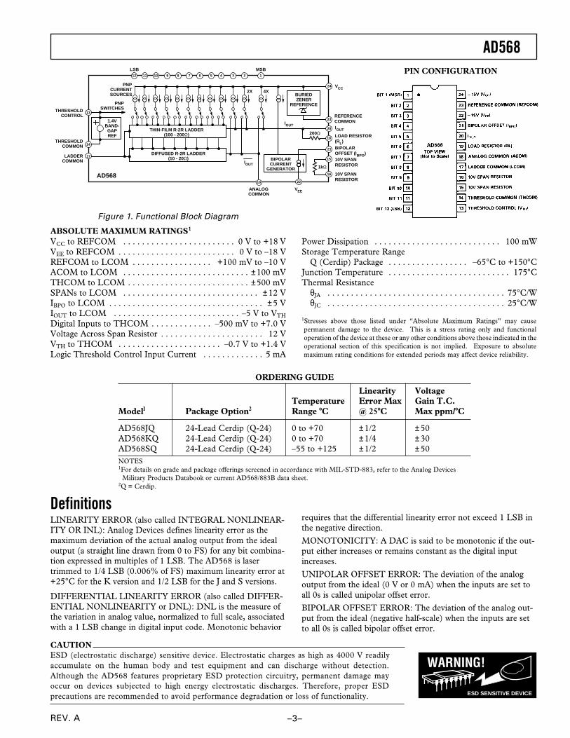
BUFFERED VOLTAGE OUTPUTFor full-scale outputs of greater than 1 V, some type of externalbuffer amplifier is required. The AD840 fills this requirementperfectly, settling to 0.025% from a 10 V full-scale step in lessthan 100 ns.
A 1 kΩ span resistor has been provided on chip for use as afeedback resistor in buffered applications. Using RSPAN (Pins 15,16) introduces a 100 mW code-dependent power source ontothe chip which may generate a slight degradation in linearity.Maximum linearity performance can be realized by using an ex-ternal span resistor.
13
16
15
14
24
23
22
21
20
19
18
17
12
11
10
9
8
1
2
3
4
7
6
5
AD568
+15V
REFCOM
–15V
IBPO
RL
ACOM
LCOM
SPAN
SPAN
THCOM
VTH
IOUT
DIGITALINPUTS
0.2µF
0.1µF
0.1µF
0.1µF
–15V+15V
ANALOGGND PLANE
DIGITALGND PLANE
DIGITALSUPPLYGROUND
100pF
+5V
ANALOGOUTPUT
ANALOGSUPPLYGROUND5pF
–VS +VS
100Ω
RTH1kΩ
AD840
AMPLIFIER NOISE GAIN: 11
Figure 8. Unipolar Output Buffered 0 to –10.24V
Unipolar Inverting ConfigurationFigure 8 shows the connections for producing a – 10.24 V full-scale swing. This configuration uses the AD568 in the currentoutput mode into a summing junction at the inverting input ter-minal of the external op amp. With the load resistor RL
grounded, the DAC has an output impedance of 100 Ω. Thisproduces a noise gain of 11 from the noninverting terminal ofthe op amp, and hence, satisfies the stability criterion of theAD840 (stable at a gain of 10). The addition of a 5 pF compen-

AD568
REV. A–6–
sation capacitor across the 1 kΩ feedback resistor produces opti-mal settling. Lower noise gain can be achieved by connecting RL
to IOUT, increasing the DAC output impedance to approximately200 Ω, and reducing the noise gain to 6 (illustrated in Figure 9).While the output in this configuration will feature improvednoise performance, it is somewhat less stable and may sufferfrom ringing. The compensation capacitance should be in-creased to 7 pF to maintain stability at this reduced gain.
13
16
15
14
24
23
22
21
20
19
18
17
12
11
10
9
8
1
2
3
4
7
6
5
AD568
+15V
REFCOM
–15V
IBPO
RL
ACOM
LCOM
SPAN
SPAN
THCOM
VTH
IOUT
DIGITALINPUTS
0.2µF
0.1µF
0.1µF
0.1µF
–15V+15V
ANALOGGND PLANE
DIGITALGND PLANE
DIGITALSUPPLYGROUND
100pF
+5V
ANALOGOUTPUT
ANALOGSUPPLYGROUND5pF
–VS +VS
100Ω
RTH1kΩ
AD840
AMPLIFIER NOISE GAIN: 11
Figure 8. Unipolar Output Buffered 0 to –10.24V
13
16
15
14
24
23
22
21
20
19
18
17
12
11
10
9
8
1
2
3
4
7
6
5
AD568
+15V
REFCOM
–15V
IBPO
RL
ACOM
LCOM
SPAN
SPAN
THCOM
VTH
IOUT
DIGITALINPUTS
0.2µF
0.1µF
0.1µF
0.1µF
–15V+15V
ANALOGGND PLANE
DIGITALGND PLANE
DIGITALSUPPLYGROUND
100pF
+5V
ANALOGOUTPUT
ANALOGSUPPLYGROUND7pF
–VS +VS
200Ω
RTH1kΩ
AD840
AMPLIFIER NOISE GAIN: 6
Figure 9. Bipolar Output Buffered ±5.12 V
Bipolar Inverting ConfigurationFigure 9 illustrates the implementation of a +5.12 V to –5.12 Vbipolar range, achieved by connecting the bipolar offset current,IBPO, to the summing junction of the external amplifier. Notethat since the amplifier is providing an inversion, the full-scaleoutput voltage is –5.12 V, while the bipolar offset voltage (allbits OFF) is +5.12 V at the amplifier output.
Noninverting ConfigurationIf a positive full-scale output voltage is required, it can be imple-mented using the AD568 in the unbuffered voltage output modefollowed by the AD840 in a noninverting configuration (Figure10). The noise gain of this topology is 10, requiring only 5 pFacross the feedback resistor to optimize settling.
13
16
15
14
24
23
22
21
20
19
18
17
12
11
10
9
8
1
2
3
4
7
6
5
AD568
+15V
REFCOM
–15V
IBPO
RL
ACOM
LCOM
SPAN
SPAN
THCOM
VTH
IOUT
DIGITALINPUTS
0.2µF
0.1µF
0.1µF
0.1µF
–15V+15V
ANALOGGNDPLANE
DIGITALSUPPLYGROUND
100pF
+5V
ANALOGOUTPUT
ANALOGSUPPLYGROUND5pF
–VS +VS
111Ω
RTH1kΩ
AD840
AMPLIFIER NOISE GAIN: 10
DIGITAL GND PLANE
Figure 10. Unipolar Output Buffered 0 V to +10.24 V
Guidelines for Using the AD568The designer who seeks to combine high speed with high preci-sion faces a challenging design environment. Where tens ofmilliamperes are involved, fractions of an ohm of misplacedimpedance can generate several LSBs of error. Increasingbandwidths make formerly negligible parasitic capacitances andinductances significant. As system performance reaches and ex-ceeds that of the measurement equipment, time-honored testmethods may no longer be trustworthy. The DAC’s placementon the boundary between the analog and digital domains intro-duces additional concerns. Proper RF techniques must be usedin board design, device selection, supply bypassing, grounding,and measurement if optimal performance is to be realized. TheAD568 has been configured to be relatively easy to use, even insome of the more treacherous applications. The device charac-teristics shown in this data sheet are readily achievable if properattention is paid to the details. Since a solid understanding ofthe circuit involved is one of the designer’s best weapons againstthe difficulties of RF design, the following sections provide illus-trations, explanations, examples, and suggestions to facilitatesuccessful design with the AD568.
Current Output vs. Voltage OutputAs indicated in Figures 3 through 10, the AD568 has beendesigned to operate in several different modes depending on theexternal circuit configuration. While these modes may becategorized by many different schemes, one of the most impor-tant distinctions to be made is whether the DAC is to be used togenerate an output voltage or an output current. In the currentoutput mode, the DAC output (Pin 20) is tied to some type ofsumming junction, and the current flowing from the DAC intothis summing junction is sensed (e.g., Figures 8 and 9). In this

AD568
REV. A –7–
The threshold of the digital inputs is set at 1.4 V and does notvary with supply voltage. This is provided by a bandgap refer-ence generator, which requires approximately 3 mA of bias cur-rent achieved by tying RTH to any +VL supply where
RTH =
+V L –1.4V3mA
The input lines operate with small input currents to easilyachieve interface with unbuffered CMOS logic. The digital in-put signals to the DAC should be isolated from the analog out-put as much as possible. To minimize undershoot, ringing, andpossible digital feedthrough noise, the interconnect distances tothe DAC inputs should be kept as short as possible. Termina-tion resistors may improve performance if the digital lines be-come too long. The digital input should be free from largeglitches and ringing and have maximum 10% to 90% rise andfall times of 5 ns. Figure 12 shows the equivalent digital inputcircuit of the AD568.
1.28mA
125Ω
RTH(EXTERNAL)
VTHRESHOLD
1.4VBANDGAPDIODE
THRESHOLDCOMMON
LADDERCOMMON
TOIOUT
TO ANALOGCOMMON
TOTHRESHOLD
COMMON
+VL
5pF
BITINPUT
58pF
Figure 12. Equivalent Digital Input
Due to the high-speed nature of the AD568, it is recommendedthat high-speed logic families such as Schottky TTL, high-speedCMOS, or the new lines of FAST* TTL be used exclusively.Table I shows how DAC performance can vary depending onthe driving logic used. As this table indicates, STTL, HCMOS,and FAST represent the most viable families for driving theAD568.
Table I. DAC Performance vs. Drive Logic1
DAC10-90% Settling Time2, 3 Maximum
Logic DAC 1% 0.1% 0.025% Glitch4 GlitchFamily Rise Time2 Impulse Excursion
TTL 11 ns 18 ns 34 ns 50 ns 2.5 nV-s 240 mVLSTTL 11 ns 28 ns 46 ns 80 ns 950 pV-s 160 mVSTTL 9.5 ns 16 ns 33 ns 50 ns 850 pV-s 150 mVHCMOS 11 ns 24 ns 38 ns 50 ns 350 pV-s 115 mVFAST* 12 ns 16 ns 36 ns 42 ns 1.0 nV-s 250 mV
NOTES1All values typical, taken in rest fixture diagrammed in Figure 13.2Measurements are made for a 1 V full-scale step into 100 Ω DAC load
resistance.3Settling time is measured from the time the digit input crosses the threshold
voltage (1.4 V) to when the output is within the specified range of its finalvalue.
4The worst case glitch impulse, measured on the major carry DAC full scaleis 1 V.
mode, the DAC output scale is insensitive to whether the loadresistor, RL, is shorted (Pin 19 connected to Pin 20), orgrounded (Pin 19 connected to Pin 18). However, this doesaffect the output impedance of the DAC current and may have asignificant impact on the noise gain of the external circuitry. Inthe voltage output mode, the DAC’s output current flowsthrough its own internal impedance (perhaps in parallel with anexternal impedance) to generate a voltage, as in Figures 3, 4, 5,and 10. In this case, the DAC output scale is directly dependenton the load impedance. The temperature coefficient of theAD568’s internal reference is trimmed in such a way that thedrift of the DAC output in the voltage output mode is centeredon zero. The current output of the DAC will have an additionaldrift factor corresponding to the absolute temperature coeffi-cient of the internal thin-film resistors. This additional drift maybe removed by judicious placement of the 1 kΩ span resistor inthe signal path. For example, in Figures 8 and 9, the currentflowing from the DAC into the summing junction could sufferfrom as much as 150 ppm/°C of thermal drift. However, sincethis current flows through the internal span resistor (Pins 15 and16) which has a temperature coefficient that matches the DACladder resistors, this drift factor is compensated and the bufferedvoltage at the amplifier output will be within specified limits forthe voltage output mode.
Output Voltage ComplianceThe AD568 has a typical output compliance range of +1.2 V to–2.0 V (with respect to the LCOM Pin). The current-steering output stages will be unaffected by changes in the out-put terminal voltage over that range. However, as shown in Fig-ure 11, there is an equivalent output impedance of 200 Ω inparallel with 15 pF at the output terminal which produces anequivalent error current if the voltage deviates from the laddercommon. This is a linear effect which does not change with in-put code. Operation beyond the maximum compliance limitsmay cause either output stage saturation or breakdown resultingin nonlinear performance. The positive compliance limit is notaffected by the positive power supply, but is a function of outputcurrent and the logic threshold voltage at VTH, Pin 13.
IOUT = 10.24mA x DIGITAL IN4096
IOUT = 10.24mA x DIGITAL IN4096
10.24mA
RLADDER(200Ω)
15pF
ANALOGCOMMON
LADDERCOMMON
RLOAD(200Ω)
15pF
COMPLIANCETO VTHRESHOLD
RLOAD IOUT
RLADDER(200Ω)
COMPLIANCE TOLOGIC LOW VALUE
(1 – )
Figure 11. Equivalent Output
Digital Input ConsiderationsThe AD568 uses a standard positive true straight binary codefor unipolar outputs (all 1s full-scale output), and an offset bi-nary code for bipolar output ranges. In the bipolar mode, withall 0s on the inputs, the output will go to negative full scale;with 111 . . . 11, the output will go to positive full scale less1 LSB; and with 100 . . 00 (only the MSB on), the output willgo to zero.

AD568
REV. A–8–
The variations in settling times can be attributed to differencesin the rise time and current driving capabilities of the variousfamilies. Differences in the glitch impulse are predominantly de-pendent upon the variation in data skew. Variations in thesespecs occur not only between logic families, but also betweendifferent gates and latches within the same family. When select-ing a gate to drive the AD568 logic input, pay particular atten-tion to the propagation delay time specs: tPLH and tPHL.Selecting the smallest delays possible will help to minimize thesettling time, while selection of gates where tPLH and tPHL areclosely matched to one another will minimize the glitch impulseresulting from data skew. Of the common latches, the 74374 oc-tal flip-flop provides the best performance in this area for manyof the logic families mentioned above.
*FAST is a registered trademark of Fairchild Camera and Instrumentation Corporation.
1A
1B
2A
2B
3A
3B
4A
4B
VCC
1V
2V
3V
4V
STROBE
GND
1A
1B
2A
2B
3A
3B
4A
4B
VCC
1V
2V
3V
4V
STROBE
GND
1A
1B
2A
2B
3A
3B
4A
4B
VCC
1V
2V
3V
4V
STROBE
GND
1
2
3
4
5
6
7
8
9
10
11
12
VCC
REFCOM
ACOM
THCON
VEE
IBPO
IOUT
RL
RSPAN
VTH
LCOM
RSPAN
AD568
+15V –15V
VOUT
1k
+5V
+5VCLOCK IN
WORD A12
12WORD B
SELECT
74158
SELECT
74158
SELECT
74158
Figure 13. Test Setup for Glitch Impulse and Settling
Time Measurements
Settling Time ConsiderationsAs can be seen from Table I and the specifications page, the set-tling time of the AD568 is application dependent. The fastestsettling is achieved in the current-output mode, since the volt-age output mode requires the output capacitance to be chargedto the appropriate voltage. The DAC’s relatively large outputcurrent helps to minimize this effect, but settling-time sensitiveapplications should avoid any unnecessary parasitic capacitanceat the output node of voltage output configurations. Direct mea-surement of the fine scale DAC settling time, even in the voltageoutput mode, is extremely tricky: analog scope front ends aregenerally incapable of recovering from overdrive quickly enoughto give an accurate settling representation. The plot shown inFigure 14 was obtained using Data Precision’s 640 16-bit sam-pling head, which features the quick overdrive recovery charac-teristic of sampling approaches combined with high accuracyand relatively small thermal tail.
TIME – ns0 12020
DA
C O
UT
PU
T –
VO
LT
S
40 60 80 100
1.026
1.024
1.022
Figure 14. Zero to Full-Scale Settling
Glitch ConsiderationsIn many high-speed DAC applications, glitch performance is acritical specification. In a conventional DAC architecture suchas the AD568 there are two basic glitch mechanisms: data skewand digital feedthrough. A thorough understanding of thesesources can help the user to minimize glitch in any application.
DIGITAL FEEDTHROUGH—As with any converter product,a high-speed digital-to-analog converter is forced to exist on thefrontier between the noisy environment of high-speed digitallogic and the sensitive analog domain. The problems of this in-terfacing are particularly acute when demands of high speed(greater than 10 MHz switching times) and high precision (12bits or more) are combined. No amount of design effort canperfectly isolate the analog portions of a DAC from the spectralcomponents of a digital input signal with a 2 ns risetime. Inevi-tably, once this digital signal is brought onto the chip, some ofits higher frequency components will find their way to the sensi-tive analog nodes, producing a digital feedthrough glitch. Tominimize the exposure to this effect, the AD568 has intention-ally omitted the on-board latches that have been included inmany slower DACs. This not only reduces the overall level ofdigital activity on chip, it also avoids bringing a latch clock pulseon board, whose opposite edge inevitably produces a substantialglitch, even when the DAC is not supposed to be changingcodes. Another path for digital noise to find its way onto a con-verter chip is through the reference input pin. The completelyinternal reference featured in the AD568 eliminates this noiseinput, providing a greater degree of signal integrity in the analogportions of the chip.
DATA SKEW—The AD568, like many of its slower predeces-sors, essentially uses each digital input line to switch a separate,weighted current to either the output (IOUT) or some other node(ANALOG COM). If the input bits are not changed simulta-neously, or if the different DAC bits switch at different speeds,then the DAC output current will momentarily take on some in-correct value. This effect is particularly troublesome at the“carry points”, where the DAC output is to change by only oneLSB, but several of the larger current sources must be switchedto realize this change. Data skew can allow the DAC output tomove a substantial amount towards full scale or zero (dependingupon the direction of the skew) when only a small transition isdesired. Great care was taken in the design and layout of theAD568 to ensure that switching times of the DAC switches aresymmetrical and that the length of the input data lines are short
AD568
REV. A –9–
and well matched. The glitch-sensitive user should be equallydiligent about minimizing the data skew at the AD568’s inputs,particularly for the 4 or 5 most significant bits. This can beachieved by using the proper logic family and gate to drive theDAC, and keeping the interconnect lines between the logic out-puts and the DAC inputs as short and as well matched as pos-sible, particularly for the most significant bits. The top 6 bitsshould be driven from the same latch chip if latches are used.
Glitch Reduction SchemesBIT-DESKEWING—Even carefully laid-out boards using theproper driving logic may suffer from some degree of data-skewinduced glitch. One common approach to reducing this effect isto add some appropriate capacitance (usually several pF) toeach of the 2 or 3 most significant bits. The exact value of eachcapacitor for a given application should be determined experi-mentally, as it will be dependent on circuit board layout and thetype of driving logic used. Table II presents a few examples ofhow the glitch impulse may be reduced through passivedeskewing.
Table II. Bit Delay Glitch Reduction Examples1
Logic Uncompensated Compensation CompensatedFamily Gate Glitch Used Glitch
HCMOS 74157 350 pV-s C2 = 5 pF 250 pV-sSTTL 74158 850 pV-s R1 = 50 Ω, 600 pV-s
C1 = 7 pF
NOTE1Measurements were made using a modified version of the fixture shown inFigure 13, with resistors and capacitors placed as shown in Figure 15. Resis-tance and capacitance values were set to zero except as noted.
As Figure 15 indicates, in some cases it may prove useful toplace a few hundred ohms of series resistance in the input lineto enhance the delay effect. This approach also helps to reducesome of the digital feedthrough glitch, as the higher frequencyspectral components are being filtered out of the most signifi-cant bits’ digital inputs.
1
2
3
4
5
6
R1
R2
R3
FROMDRIVING
LOGIC
BIT 1 (MSB)
BIT 2
BIT 3
BIT 4
BIT 5
BIT 6
AD568
R – C BIT DESKEWING SCHEME
Figure 15. R-C Bit Deskewing Scheme
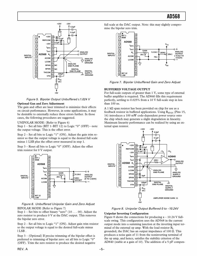
THRESHOLD SHIFT—It is also possible to reduce the dataskew by shifting the level of logic voltage threshold, VTH (Pin13). This can be readily accomplished by inserting some resis-tance between the THRESHOLD COM pin (Pin 14) andground, as in Figure 16. To generate threshold voltages below
1.4 V, Pin 13 may be directly driven with a voltage source, leav-ing Pin 14 tied to the ground plane. As Note 2 in Table III indi-cates, lowering the threshold voltage may reduce output voltagecompliance below the specified limits, which may be of concernin an unbuffered voltage output topology.
14
13
+5V
RA
RBTHCOM
VTH
C1
AD568C1: 1000pF CHIP CAPACITOR
ANALOGGROUNDPLANE
Figure 16. Positive Threshold Voltage Shift
Table III shows the glitch reduction achieved by shifting thethreshold voltage for HCMOS, STTL, and FAST logic.
Table III. Threshold Shift for Glitch Improvement1
Logic Uncompensated Modified ResultingFamily Gate Glitch Threshold2 Glitch
HCMOS 74HC158 350 pV-s 1.7 V 150 pV-sSTTL 74S158 850 pV-s 1.0 V 200 pV-sFAST 74F158 1000 pV-s 1.3 V 480 pV-s
NOTES1Measurements made on a modified version of the circuit shown in Figure 13,with a 1 V full scale.
2Use care in any scheme that lowers the threshold voltage since the output volt-age compliance of the DAC is sensitive to this voltage. If the DAC is to be op-erating in the voltage output mode, it is strongly suggested that the thresholdvoltage be set at least 200 mV above the output voltage full scale.
DeglitchingSome applications may prove so sensitive to glitch impulse thatreduction of glitch impulse by an order of magnitude or more isrequired. In order to realize glitch impulses this low, some sortof sample-and-hold amplifier (SHA)-based deglitching schememust be used.
There are high-speed SHAs available with specifications suffi-cient to deglitch the AD568, however most are hybrid in designat costs which can be prohibitive. A high performance, low costalternative shown in Figure 17 is a discrete SHA utilizing ahigh-speed monolithic op amp and high-speed DMOS FETswitches.
This SHA circuit uses the inverting integrator architecture. TheAD841 operational amplifier used (300 MHz gain bandwidthproduct) is fabricated on the same high-speed process as theAD568. The time constant formed by the 200 Ω resistor and the100 pF capacitor determines the acquisition time and also bandlimits the output signal to eliminate slew induced distortion.
A discrete drive circuit is used to achieve the best performancefrom the SD5000 quad DMOS switch. This switch driving cellis composed of MPS571 RF npn transistors and an MC10124TTL to ECL translator. Using this technique provides bothhigh speed and highly symmetrical drive signals for the SD5000switches. The switches are arranged in a single-throw double-pole (SPDT) configuration. The 360 pF “flyback” capacitor isswitched to the op amp summing junction during the hold modeto keep switching transients from feeding to the output. The ca-pacitor is grounded during sample mode to minimize its effecton acquisition time.

AD568
REV. A–10–
Circuit layout for a high speed SHA is almost as critical as thedesign itself. Figure 17 shows a recommended layout of thedeglitching cell for a double sided printed circuit board. Thelayout is very compact with care taken that all critical signalpaths are short.
–5V
MC10124 249Ω
169Ω510Ω
360Ω360Ω
–5V
169Ω
249Ω
500pF
OUTPUT
75Ω
200Ω200Ω
IN4735
+15V
–15V
–15V
20kΩ
1.6Ω 0.39µF
TO PIN 2SD5000
100pF
4
5
10
11
916
14
13 12
6 8
5
43
1
AD841
Figure 17. High Performance Deglitcher
Grounding RulesThe AD568 brings out separate reference, output, and digitalpower grounds. This allows for optimum management of signalground currents for low noise and high-speed-settling perfor-mance. The separate ground returns are provided to minimizechanges in current flow in the analog signal paths. In this way,logic return currents are not summed into the same return pathwith the analog signals.
It is important to understand which supply and signal currentsare flowing in which grounds so that they may be returned tothe proper power supply in the best possible way.
The majority of the current that flows into the VCC supply (Pin24) flows out (depending on the DAC input code) either theANALOG COMMON (Pin 18), the LADDER COMMON(Pin 17), and/or IOUT (Pin 20).
The current in the LADDER COMMON is configured to becode independent when the output current is being summedinto a virtual ground. If IOUT is operated into its own output im-pedance (or in any unbuffered voltage output mode) the currentin LADDER COMMON will become partially code dependent.
The current in the ANALOG COMMON (Pin 18) is an ap-proximate complement of the current in IOUT, i.e., zero whenthe DAC is at full scale and approximately 10 mA at zero inputcode.
A relatively constant current (not code dependent) flows out theREFERENCE COMMON (Pin 23).
The current flowing out of the VEE supply (Pin 22) comes froma combination of reference ground and BIPOLAR OFFSET(Pin 21). The plus and minus 15 V supplies are decoupled tothe REFERENCE COMMON.
The ground side of the load resistor RL, ANALOG COMMONand LADDER COMMON should be tied together as close tothe package pins as possible. The analog output voltage is thenreferred to this node and thus it becomes the “high quality”
ground for the AD568. The REFERENCE COMMON (andBipolar offset when not used), should also be connected to thisnode.
All of the current that flows into the VTH terminal (Pin 13) fromthe resistor tied to the 5 V logic supply (or other convenientpositive supply) flows out the THRESHOLD COMMON (Pin14). This ground pin should be returned directly to the digitalground plane on its own individual line.
The +5 V logic supply should be decoupled to the THRESH-OLD COMMON.
Because the VTH pin is connected directly to the DAC switchesit should be decoupled to the analog output signal common.
In order to preserve proper operation of the DAC switches, thedigital and analog grounds need to eventually be tied together.This connection between the ground planes should be madewithin 1/2" of the DAC.
The Use of Ground and Power PlanesIf used properly, ground planes can perform a myriad of func-tions on high-speed circuit boards: bypassing, shielding, currenttransport, etc. In mixed signal design, the analog and digital por-tions of the board should be distinct from one another, with theanalog ground plane covering analog signal traces and the digitalground plane confined to areas covering digital interconnect.
The two ground planes should be connected at or near theDAC. Care should be taken to insure that the ground plane isuninterrupted over crucial signal paths. On the digital side, thisincludes the digital input lines running to the DAC and anyclock lines. On the analog side, this incudes the DAC outputsignal as well as the supply feeders. The use of side runs orplanes in the routing of power lines is also recommended. Thisserves the dual function of providing a low series impedancepower supply to the part as well as providing some ‘‘free’’ ca-pacitive decoupling to the appropriate ground plane. Figure18 illustrates many of the points discussed above. If more layersof interconnect are available, even better results are possible.
Using the Right Bypass CapacitorsProbably the most important external components associatedwith any high-speed design are the capacitors used to bypassthe power supplies. Both selection and placement of these ca-pacitors can be critical and, to a large extent, dependent uponthe specifics of the system configurations. The dominant consid-eration in selection of bypass capacitors for the AD568 is mini-mization of series resistance and inductance. Many capacitorswill begin to look inductive at 20 MHz and above, the very fre-quencies we are most interested in bypassing. Ceramic and film-type capacitors generally feature lower series inductance thantantalum or electrolytic types. A few general rules are of univer-sal use when approaching the problem of bypassing:
Bypass capacitors should be installed on the printed circuitboard with the shortest possible leads consistent with reliableconstruction. This helps to minimize series inductance in theleads. Chip capacitors are optimal in this respect.
Some series inductance between the DAC supply pins and thepower supply plane often helps to filter out high-frequencypower supply noise. This inductance can be generated using asmall ferrite bead.

AD568
REV. A –11–
5V
DIGITAL GROUNDPLANE
CLOCKANALOG GROUND
PLANE
+15V
–15V
OUTPUT
5V
INPUTWORDS
AD568SETTLING/GLITCH
EVALUATION BOARD
Component Side
ANALOG +5V
+5V
ANALOG VCC
ANALOG VEE
Foil Side
Figure 18. Printed Circuit Board Layout
High-Speed Interconnect and RoutingIt is essential that care be taken in the signal and power groundcircuits to avoid inducing extraneous voltage drops in the signalground paths. It is suggested that all connections be short anddirect, and as physically close to the package as possible, so thatthe length of any conduction path shared by external compo-nents will be minimized. When runs exceed an inch or so inlength, some type of termination resistor may be required. Thenecessity and value of this resistor will be dependent upon thelogic family used.
For maximum ac performance, the DAC should be mounted di-rectly to the circuit board; sockets should not be used as they in-troduce unwanted capacitive coupling between adjacent pins ofthe device.
Applications1 ms, 12-BIT SUCCESSIVE APPROXIMATION A/DCONVERTERThe AD568’s unique combination of high speed and true 12-bitaccuracy can be used to construct a 12-bit SAR-type A/D con-verter with a sub-µs conversion time. Figure 19 shows the con-figuration used for this application. A negative analog inputvoltage is converted into current and brought into a summingjunction with the DAC current. This summing junction isbidirectionally clamped with two Schottky diodes to limit itsvoltage excursion from ground. This voltage is differentially am-plified and passed to a high-speed comparator. The comparatoroutput is latched and fed back to the successive approximationregister, which is then clocked to generated the next set of codesfor the DAC.
13
16
15
14
24
23
22
21
20
19
18
17
+15V
REFCOM
–15V
IBPO
RL
ACOM
LCOM
SPAN
SPAN
THCOM
VTH
IOUT
12
11
10
9
8
1
2
3
4
7
6
5 DAC
AD568
0.2µF
0.1µF
0.1µF
0.1µF
–15V+15V
ANALOGGND PLANE
100pF
1k
+5V
NC
NC
4
7
6
5
21
20
19
18
17
16
9
8
Q11
Q10
Q9
Q8
Q6
Q5
Q4
Q3
Q2
Q1
Q0
Q7
11
3
14
1
13
24
12
2
23
22
15
10
VCC
GND
D0
Q11
NC
NC
CP
E
S
CC
D
NC
+5V
PARALLEL DATAOUT
SAR2504
0.01µF
1k620 620
2.5k
VI0 TO –10.24V
N +5V –5V
–5V
1k
150
Q1 Q2
Q3
D1 D227k
–15V
1
2
3
4
8
7
6
5
V+
+IN
V–
–IN
OUT
OUT
LCH
GND
COMPARATORLT1016
D3
IN4148
CONVERSION COMPLETE
START COMVERT
CHIP ENABLE
150kΩ
+5V
INVERTER74HC04
15kΩ150kΩ
Q4
Q5
Figure 19. AD568 1 µs Successive Approximation A/D Application

AD568
REV. A–12–
Circuit DetailsFigure 20 shows an approximate timing budget for the A/D con-verter. If 12 cycles are to be completed in 1 µs, approximately80 ns is allowed for each cycle. Since the Schottky diodes clampthe voltage of the summing junction, the DAC settling time ap-proaches the current-settling value of 35 ns, and hence uses upless than half the timing budget.
To maintain simplicity, a simple clock is used that runs at aconstant rate throughout the conversion, with a duty cycle ofapproximately 90%. If absolute speed is worth the additionalcomplexity, the clock frequency can be increased as the conver-sion progresses since the DAC must settle from increasinglysmaller steps.
When seeking a cycle time of less than 100 ns, the delays gener-ated by the older generation SAR registers become problematic.Newer, high speed SAR logic chips are becoming available inthe classic 2504 pinout that cuts the logic overhead in half. Oneexample of this is Zyrel’s ZR2504.
Finding a comparator capable of keeping up with this DAC ar-rangement is fairly difficult: it must respond to an overdrive of250 µV (1 LSB) in less than 25 ns. Since no inexpensive com-parator exists with these specs, special arrangements must bemade. The LT106 comparator provides relatively quick re-sponse, but requires at least 5 mV of overdrive to maintain thisspeed. A discrete preamplifier may be used to amplify the sum-ming junction voltage to sufficiently overdrive the comparator.Care must be exercised in the layout of the preamp/comparatorblock to avoid introducing comparator instability with thepreamp’s additional gain.
10ns 35ns 15ns 10ns 10ns
0 10ns 20ns 30ns 40ns 50ns 60ns 70ns 80ns
CLOCKPULSE
START OF NEXTCLOCK CYCLE
LATCH COMPARATOR
START OFCLOCK CYCLE
SARDELAY DAC SETTLING
PREAMPDELAY
COMPARATORDELAY
Figure 20. Typical Clock Cycle for a 1 µs SAR A/D
Converter
HIGH-SPEED MULTIPLYING DACA powerful use for the AD568 is found in multiplying applica-tions, where the DAC controls the amplitude of a high-speedsignal. Specifically, using the AD568 as the control voltageinput signal for the AD539 60 MHz analog multiplier and
AD5539 wideband op amp, a high-speed multiplying DAC canbe built.
In the application shown in Figure 21, the AD568 is used in abuffered voltage output mode to generate the input to theAD539’s control channel. The speed of the AD568 allowsoversampling of the control signal waveform voltage, therebyproviding increased spectral purity of the amplitude envelopethat modulates the analog input channels.
The AD568 is configured in the unbuffered unipolar outputmode. The internal 200 Ω load resistor creates the 0-1 V FSoutput signal, which is buffered and amplified to a 0-3 V rangesuitable for the control channel of the AD539.
A 500 Ω input impedance exists at Pin 1, the input channel. Toprovide a buffer for the 0-1 V output signal from the AD568looking into the impedance and to achieve the full-scale range,the AD841, high-speed, fast settling op amp is included. Thegain of 3 is achieved with a 2 kΩ resistor configured in followermode with a 1 kΩ pot and 500 Ω resistor. A 20 kΩ pot withconnections to Pins 3, 4 and 12 is provided for offset trim.
The AD539 can accept two separate input signals, each with anominal full-scale voltage range of ±2 V. Each signal can thenbe simultaneously controlled by the AD568 signal at the com-mon input channels, Pins 11 and 14, applied to the AD5539 ina subtracting configuration, provide the voltage output signal:
VOUT =
D4096
×VY1 –VY 2
2V(0≤D ≤4095)
For applications where only a single channel is involved, chan-nel 2, VY2, is tied to ground. This provides:
VOUT =
D4096
×VY1
2V(0≤D ≤4095)
Some AD539 circuit details: The control amplifier compensa-tion capacitor for Pin 2, CC, must have a minimum value of300 pF to provide circuit stability. For improved bandwidth andfeedthrough, the feedthrough capacitor between Pins 1 and 2should be 5-20% of CC. A Schottky diode at Pin 2 can improverecovery time from small negative values of VX. Lead lengthsalong the path of the high-speed signal from AD568 should bekept at a minimum.

AD568
REV. A –13–
16
15
13
16
15
14
24
23
22
21
20
19
18
17
12
11
10
9
8
1
2
3
4
7
6
5
AD568
+15V
REFCOM
–15V
IBPO
RL
ACOM
LCOM
SPAN
SPAN
THCOM
VTH
IOUT
DIGITALINPUTS
0.2µF
0.1µF
0.1µF
0.1µF
–15V+15V
ANALOGGND PLANE
DIGITALGND PLANE DIGITAL
SUPPLYGROUND
100pF
RTH1kΩ
+5V
NC
NC
ANALOGOUTPUT
ANALOGSUPPLYGROUND
43
10
12
6
5Cff100pF
Cc3000pF
75Ω
1µF
1µF
–VS
20kΩ
AD841
2kΩ1kΩ
500Ω
+VS
13
14
1
2
3
4
5
6
7
8 9
10
11
12
AD568
W1
Z1
CH1OUTPUT
BASECOMMON
Z2
W2
CH2OUTPUT
11
+VS
–VS
CONTROL
HFCOMP
CH1INPUT
INPUTCOMMON
OUTPUTCOMMON
CH2INPUT
VX
75Ω
VY1IN
VY1IN
10Ω
10Ω
+9V
–9V
200ΩGAIN
ADJUST(±4% RANGE)
10
7
1
14
–9V
AD5539N 8
100k
180Ω
470Ω
2.7Ω 0.47µF
–9V
50k(OPTIONAL)OUTPUTOFFSET
–9V
+9V
+9V
0.47µF2.7Ω
VOUT
3
D1
180Ω
CF
0.25pF –1.5pF
D1: THOMPSON CSFBAR – 10 OR SIMILAR SCHOTTKY DIODE
SHORT, DIRECT CONNECTION TO GROUND PLANE.
Figure 21. Wideband Digitally Controlled Multiplier
OUTLINE DIMENSIONSDimensions shown in inches and (mm).
24-Pin Cerdip (Suffix Q)

C1
01
4a
–9
–7
/87
PR
INT
ED
IN
U.S
.A.
–14–

![Crystals with Ultrahigh Piezoelectricityvixra.org/pdf/2001.0316v1.pdfCrystals with Ultrahigh Piezoelectricity ... smartphones to advanced microprocessors. [26] ... probabilistic smears](https://static.fdocuments.in/doc/165x107/6045ca6abb58fa5d2f40bf63/crystals-with-ultrahigh-p-crystals-with-ultrahigh-piezoelectricity-smartphones.jpg)