ACT8945AQJ305-PK020 Rev G
46
ACT8945A Advanced PMU for Atmel SAMA5Dx Series & SAM9 Series Processors Data Sheet Rev. G, January 2020 | Subject to change without notice 1 of 46 www.qorvo.com © 2020 Qorvo US, Inc. All rights reserved. FEATURES • Three Step-Down DC/DC Converters • Four Low-Dropout Linear Regulators • Integrated ActivePath TM Charger • I 2 C TM Serial Interface • Advanced Enable/Disable Sequencing Controller • Minimal External Components • Tiny 5×5mm TQFN55-40 Package - 0.75mm Package Height - Pb-Free and RoHS Compliant GENERAL DESCRIPTION The ACT8945A is a complete, cost effective, highly- efficient ActivePM TM power management solution, optimized for the unique power, voltage- sequencing, and control requirements of the Atmel SAMA5D3 series: SAMA5D[31/33/34/35/36], and Atmel SAM9 series: SAM9G[15/25/35/45/46], SAM9X[25/35], SAM9M[10/11], SAM9N[11/12] processors. It is ideal for a wide range of high performance portable handheld applications such as human-machine interfaces, control panels, smart grid infrastructures, network gateways, M2M systems, 2D barcode scanners, barcode printers, machine vision equipment, as well as home and commercial building automations, POS terminals, medical devices and white goods. This device integrates the ActivePath TM complete battery charging and management system with seven power supply channels. This device features three step-down DC/DC converters and four low-noise, low-dropout linear regulators, along with a complete battery charging solution featuring the advanced ActivePath TM system-power selection function. The three DC/DC converters utilize a high- efficiency, fixed-frequency (2MHz), current-mode PWM control architecture that requires a minimum number of external components. Two DC/DCs are capable of supplying up to 1100mA of output current, while the third supports up to 1200mA. All four low-dropout linear regulators are high- performance, low-noise regulators that supply up to 320mA of output current. The ACT8945A is available in a compact, Pb-Free and RoHS-compliant TQFN55-40 package TYPICAL APPLICATION DIAGRAM
Transcript of ACT8945AQJ305-PK020 Rev G

ACT8945A
Advanced PMU for Atmel SAMA5Dx Series & SAM9 Series Processors
Data Sheet Rev. G, January 2020 | Subject to change without notice 1 of 46 www.qorvo.com
© 2020 Qorvo US, Inc. All rights reserved.
FEATURES
• Three Step-Down DC/DC Converters
• Four Low-Dropout Linear Regulators
• Integrated ActivePathTM Charger
• I2CTM Serial Interface
• Advanced Enable/Disable Sequencing Controller
• Minimal External Components
• Tiny 5×5mm TQFN55-40 Package
− 0.75mm Package Height
− Pb-Free and RoHS Compliant
GENERAL DESCRIPTION
The ACT8945A is a complete, cost effective, highly-
efficient ActivePMTM power management solution,
optimized for the unique power, voltage- sequencing,
and control requirements of the Atmel SAMA5D3 series:
SAMA5D[31/33/34/35/36], and Atmel SAM9 series:
SAM9G[15/25/35/45/46], SAM9X[25/35], SAM9M[10/11],
SAM9N[11/12] processors. It is ideal for a wide range of
high performance portable handheld applications such as
human-machine interfaces, control panels, smart grid
infrastructures, network gateways, M2M systems, 2D
barcode scanners, barcode printers, machine vision
equipment, as well as home and commercial building
automations, POS terminals, medical devices and white
goods. This device integrates the ActivePathTM complete
battery charging and management system with seven
power supply channels.
This device features three step-down DC/DC
converters and four low-noise, low-dropout linear
regulators, along with a complete battery charging
solution featuring the advanced ActivePathTM
system-power selection function.
The three DC/DC converters utilize a high-
efficiency, fixed-frequency (2MHz), current-mode
PWM control architecture that requires a minimum
number of external components. Two DC/DCs are
capable of supplying up to 1100mA of output
current, while the third supports up to 1200mA. All
four low-dropout linear regulators are high-
performance, low-noise regulators that supply up to
320mA of output current.
The ACT8945A is available in a compact, Pb-Free
and RoHS-compliant TQFN55-40 package
TYPICAL APPLICATION DIAGRAM

Data Sheet Rev. G, January 2020 | Subject to change without notice 2 of 46 www.qorvo.com
© 2020 Qorvo US, Inc. All rights reserved.
ACT8945A
Advanced PMU for Atmel SAMA5Dx Series & SAM9 Series Processors
TABLE OF CONTENTS
General Information ..................................................................................................................................................... p. 01
Functional Block Diagram ............................................................................................................. p. 04
Ordering Information ................................................................................................................................................... p. 05
Pin Configuration ......................................................................................................................................................... p. 05
Pin Descriptions .......................................................................................................................................................... p. 06
Absolute Maximum Ratings ......................................................................................................................................... p. 08
I2C Interface Electrical Characteristics ........................................................................................................................ p. 09
Global Register Map .................................................................................................................................................... p. 10
Register and Bit Descriptions ...................................................................................................................................... p. 11
System Control Electrical Characteristics.................................................................................................................... p. 16
Step-Down DC/DC Electrical Characteristics .............................................................................................................. p. 17
Low-Noise LDO Electrical Characteristics................................................................................................................... p. 18
ActivePathTM Charger Electrical Characteristics ......................................................................................................... p. 19
Typical Performance Characteristics ........................................................................................................................... p. 21
System Control Information ......................................................................................................................................... p. 27
Interfacing with the Atmel SAMA5D3 Series & SAM9 Series Processors ................................................................... p. 27
Control Signals .............................................................................................................................................. p. 28
Push-Button Control ...................................................................................................................................... p. 29
Control Sequences ........................................................................................................................................ p. 29
Functional Description ................................................................................................................................................. p. 30
I2C Interface ................................................................................................................................................... p. 30
Voltage Monitor and Interrupt ........................................................................................................................ p. 30
Thermal Shutdown ........................................................................................................................................ p. 31
Step-Down DC/DC Regulators .................................................................................................................................... p. 32
General Description ....................................................................................................................................... p. 32
100% Duty Cycle Operation .......................................................................................................................... p. 32
Synchronous Rectification ............................................................................................................................. p. 32
Soft-Start........................................................................................................................................................ p. 32
Compensation ............................................................................................................................................... p. 32
Configuration Options .................................................................................................................................... p. 32
OK[ ] and Output Fault Interrupt .................................................................................................................... p. 33
PCB Layout Considerations........................................................................................................................... p. 33
Low-Noise, Low-Dropout Linear Regulators ................................................................................................................ p. 35
General Description ....................................................................................................................................... p. 35
Output Current Limit ...................................................................................................................................... p. 35
Compensation ............................................................................................................................................... p. 35
Configuration Options .................................................................................................................................... p. 35
OK[ ] and Output Fault Interrupt .................................................................................................................... p. 35
PCB Layout Considerations........................................................................................................................... p. 35
ActivePathTM Charger .................................................................................................................................................. p. 37
General Description ....................................................................................................................................... p. 37
ActivePath Architecture ................................................................................................................................. p. 37
System Configuration Optimization ............................................................................................................... p. 37
Input Protection .............................................................................................................................................. p. 37
Battery Management ..................................................................................................................................... p. 37

Data Sheet Rev. G, January 2020 | Subject to change without notice 3 of 46 www.qorvo.com
© 2020 Qorvo US, Inc. All rights reserved.
ACT8945A
Advanced PMU for Atmel SAMA5Dx Series & SAM9 Series Processors
Charge Current Programming ....................................................................................................................... p. 38
Charger Input Interrupts................................................................................................................................. p. 38
Charge-Control State Machine ...................................................................................................................... p. 41
State Machine Interrupts................................................................................................................................ p. 41
Thermal Regulation ....................................................................................................................................... p. 42
Charge Safety Timers .................................................................................................................................... p. 42
Charger Timer Interrupts ............................................................................................................................... p. 42
Charge Status Indicator ................................................................................................................................. p. 42
Reverse-Current Protection ........................................................................................................................... p. 42
Battery Temperature Monitoring .................................................................................................................... p. 42
Battery Temperature Interrupts ..................................................................................................................... p. 43
Errata Info .................................................................................................................................................................... p. 44
Errata Name .................................................................................................................................................. p. 44
Device Identification ....................................................................................................................................... p. 44
Description ..................................................................................................................................................... p. 44
Recommendation ........................................................................................................................................... p. 44
Workaround .................................................................................................................................................... p. 44
Package Outline and Dimensions ............................................................................................................................... p. 45

Data Sheet Rev. G, January 2020 | Subject to change without notice 4 of 46 www.qorvo.com
© 2020 Qorvo US, Inc. All rights reserved.
ACT8945A
Advanced PMU for Atmel SAMA5Dx Series & SAM9 Series Processors
FUNCTIONAL BLOCK DIAGRAM

Data Sheet Rev. G, January 2020 | Subject to change without notice 5 of 46 www.qorvo.com
© 2020 Qorvo US, Inc. All rights reserved.
ACT8945A
Advanced PMU for Atmel SAMA5Dx Series & SAM9 Series Processors
ORDERING INFORMATION
PART NUMBER VOUT1/
VSTBY1
VOUT2/ VSTBY2
VOUT3/ VSTBY3
VOUT4 VOUT5 VOUT6 VOUT7 PACKAGE PINS TEMPERATURE
RANGE
ACT8945AQJ305-T 1.8V/1.8V 1.2V/1.0V 3.3V/3.3V 2.5V 3.3V OFF OFF TQFN55-40 40 -40°C to +85°C
ACT8945AQJ405-T 1.5V/1.35V 1.2V/1.2V 3.3V/3.3V 2.5V 3.3V OFF OFF TQFN55-40 40 -40°C to +85°C
: Standard product options are listed in this table. Contact factory for custom options. Minimum order quantity is 15,000 units.
: To select VSTBYx as the output regulation voltage for REGx, drive VSEL to logic high. VSTBYx can be set by software via I2C interface. Refer to
appropriate sections of this datasheet for VSTBYx setting.
: VOUT1 = 1.35V @VSEL=VIN and VOUT1 = 1.5V @VSEL=0 for ACT8945AQJ405-T regulator setting.
PIN CONFIGURATION
TOP VIEW
Thin - QFN (TQFN55-40)

Data Sheet Rev. G, January 2020 | Subject to change without notice 6 of 46 www.qorvo.com
© 2020 Qorvo US, Inc. All rights reserved.
ACT8945A
Advanced PMU for Atmel SAMA5Dx Series & SAM9 Series Processors
PIN DESCRIPTIONS
PIN NAME DESCRIPTION
1 REFBP Reference Bypass. Connect a 0.047μF ceramic capacitor from REFBP to GA. This pin is discharged to GA in shutdown.
2 OUT1 Output Feedback Sense for REG1.
3 GA Analog Ground. Connect GA directly to a quiet ground node. Connect GA, GP12 and GP3 together at a single point as close to the IC as possible.
4 OUT4 REG4 output. Capable of delivering up to 320mA of output current. Connect a 3.3µF ceramic capacitor from OUT4 to GA. The output is discharged to GA with 1.5kΩ resistor when disabled.
5 OUT5 REG5 output. Capable of delivering up to 320mA of output current. Connect a 3.3µF ceramic capacitor from OUT5 to GA. The output is discharged to GA with 1.5kΩ resistor when disabled.
6 INL Power Input for REG4, REG5, REG6, and REG7. Bypass to GA with a high quality ceramic capacitor placed as close to the IC as possible.
7 OUT7 REG7 output. Capable of delivering up to 320mA of output current. Connect a 3.3µF ceramic capacitor from OUT7 to GA. The output is discharged to GA with 1.5kΩ resistor when disabled.
8 OUT6 REG6 output. Capable of delivering up to 320mA of output current. Connect a 3.3µF ceramic capacitor from OUT6 to GA. The output is discharged to GA with 1.5kΩ resistor when disabled.
9 nPBIN Master Enable Input. Drive nPBIN to GA through a 50kΩ resistor to enable the IC, drive nPBIN directly to GA to assert a manual reset condition. Refer to the nPBIN Multi-Function Input section for more information. nPBIN is internally pulled up to VSYS through a 35kΩ resistor.
10 PWRHLD Power Hold Input. Enable input for all regulators. PWRHLD is internally pulled down to GA through a 500kΩ resistor. Refer to the Control Sequences section for more information.
11 nRSTO Active Low Reset Output. See the nRSTO Output section for more information.
12 nIRQ Open-Drain Interrupt Output. nIRQ is asserted any time an unmasked fault condition exists or a charger interrupt occurs. See the nIRQ Output section for more information.
13 nPBSTAT Active-Low Open-Drain Push-Button Status Output. nPBSTAT is asserted low whenever the nPBIN is pushed, and is high-Z otherwise. See the nPBSTAT Output section for more information.
14 GP3 Power Ground for REG3. Connect GA, GP12, and GP3 together at a single point as close to the IC as possible.
15 SW3 Switching Node Output for REG3.
16 VP3 Power Input for REG3. Bypass to GP3 with a high quality ceramic capacitor placed as close to the IC as possible.
17 OUT3 Output Feedback Sense for REG3.
18 PWREN Power Enable Input. Refer to the Control Sequences section for more information.
19 nLBO Low Battery Indicator Output. nLBO is asserted low whenever the voltage at LBI is lower than 1.2V, and is high-Z otherwise. See the Precision Voltage Detector section for more information.
20 LBI Low Battery Input. The input voltage is compared to 1.2V and the output of this comparison drives nLBO. See the Precision Voltage Detector section for more information.
21 ACIN AC Input Supply Detection. See the Charge Current Programming section for more information.
22 CHGLEV Charge Current Selection Input. See the Charge Current Programming section for more information.

Data Sheet Rev. G, January 2020 | Subject to change without notice 7 of 46 www.qorvo.com
© 2020 Qorvo US, Inc. All rights reserved.
ACT8945A
Advanced PMU for Atmel SAMA5Dx Series & SAM9 Series Processors
PIN DESCRIPTIONS CONT’D
PIN NAME DESCRIPTION
23 ISET Charge Current Set. Program the charge current by connecting a resistor (RISET) between ISET and GA.
See the Charge Current Programming section for more information.
24 TH Temperature Sensing Input. Connect to battery thermistor. TH is pulled up with a 102µA (typ) current internally. See the Battery Temperature Monitoring section for more information.
25 VSEL Step-Down DC/DCs Output Voltage Selection. Drive to logic low to select default output voltage. Drive to logic high to select secondary output voltage. See the Output Voltage Programming section for more information.
26 SCL Clock Input for I2C Serial Interface.
27 SDA Data Input for I2C Serial Interface. Data is read on the rising edge of SCL.
28 nSTAT Active-Low Open-Drain Charger Status Output. nSTAT has a 8mA (typ) current limit, allowing it to directly drive an indicator LED without additional external components. See the Charge Status Indicator section for more information.
29, 30 BAT Battery Charger Output. Connect this pin directly to the battery anode (+ terminal)
31, 32 VSYS System Output Pin. Bypass to GA with a 10µF or larger ceramic capacitor.
33 CHGIN Power Input for the Battery Charger. Bypass CHGIN to GA with a capacitor placed as close to the IC as possible.
34 OUT2 Output Feedback Sense for REG2.
35 VP2 Power Input for REG2. Bypass to GP12 with a high quality ceramic capacitor placed as close to the IC as possible.
36 SW2 Switching Node Output for REG2.
37 GP12 Power Ground for REG1 and REG2. Connect GA, GP12 and GP3 together at a single point as close to the IC as possible.
38 SW1 Switching Node Output for REG1.
39 VP1 Power Input for REG1. Bypass to GP12 with a high quality ceramic capacitor placed as close to the IC as possible.
40 NC1 No Connect. Not internally connected.
EP EP Exposed Pad. Must be soldered to ground on PCB.

Data Sheet Rev. G, January 2020 | Subject to change without notice 8 of 46 www.qorvo.com
© 2020 Qorvo US, Inc. All rights reserved.
ACT8945A
Advanced PMU for Atmel SAMA5Dx Series & SAM9 Series Processors
ABSOLUTE MAXIMUM RATINGS
PARAMETER VALUE UNIT
VP1, VP2 to GP12 VP3 to GP3 -0.3 to + 6 V
BAT, VSYS, INL to GA -0.3 to + 6 V
CHGIN to GA -0.3 to + 14 V
SW1, OUT1 to GP12 -0.3 to (VVP1 + 0.3) V
SW2, OUT2 to GP12 -0.3 to (VVP2 + 0.3) V
SW3, OUT3 to GP3 -0.3 to (VVP3 + 0.3) V
nIRQ, nLBO, nPBSTAT, nRSTO, nSTAT to GA -0.3 to + 6 V
nPBIN, ACIN, CHGLEV, ISET, LBI, PWRHLD, PWREN, REFBP, SCL, SDA, TH, VSEL to GA -0.3 to (VSYS + 0.3) V
OUT4, OUT5, OUT6, OUT7 to GA -0.3 to (VINL + 0.3) V
GP12, GP3 to GA -0.3 to + 0.3 V
Operating Ambient Temperature -40 to 85 °C
Maximum Junction Temperature 125 °C
Maximum Power Dissipation
TQFN55-40 (Thermal Resistance θJA = 30oC/W)
2.7 W
Storage Temperature -65 to 150 °C
Lead Temperature (Soldering, 10 sec) 300 °C
: Do not exceed these limits to prevent damage to the device. Exposure to absolute maximum rating conditions for long periods may affect
device reliability.

Data Sheet Rev. G, January 2020 | Subject to change without notice 9 of 46 www.qorvo.com
© 2020 Qorvo US, Inc. All rights reserved.
ACT8945A
Advanced PMU for Atmel SAMA5Dx Series & SAM9 Series Processors
I2C INTERFACE ELECTRICAL CHARACTERISTICS (VVSYS = 3.6V, TA = 25°C, unless otherwise specified.)
PARAMETER TEST CONDITIONS MIN TYP MAX UNIT
SCL, SDA Input Low VVSYS = 3.1V to 5.5V, TA = -40ºC to 85ºC 0.35 V
SCL, SDA Input High VVSYS = 3.1V to 5.5V, TA = -40ºC to 85ºC 1.55 V
SDA Leakage Current 1 µA
SCL Leakage Current 2 µA
SDA Output Low IOL = 5mA 0.35 V
SCL Clock Period, tSCL 1.5 µs
SDA Data Setup Time, tSU 100 ns
SDA Data Hold Time, tHD 300 ns
Start Setup Time, tST For Start Condition 100 ns
Stop Setup Time, tSP For Stop Condition 100 ns
Figure 1:
I2C Compatible Serial Bus Timing

Data Sheet Rev. G, January 2020 | Subject to change without notice 10 of 46 www.qorvo.com
© 2020 Qorvo US, Inc. All rights reserved.
ACT8945A
Advanced PMU for Atmel SAMA5Dx Series & SAM9 Series Processors
GLOBAL REGISTER MAP
: Default values of ACT8945AQJ305.
2: All bits are automatically cleared to default values when the input power is removed or falls below the system UVLO.
OUTPUT ADDRESS BITS
D7 D6 D5 D4 D3 D2 D1 D0
SYS 0x00 NAME TRST nSYSMODE nSYSLEVMSK nSYSSTAT SYSLEV[3] SYSLEV[2] SYSLEV[1] SYSLEV[0]
DEFAULT 1 1 0 R 0 1 1 1
SYS 0x01 NAME Reserved Reserved MSTROFF Reserved SCRATCH SCRATCH SCRATCH SCRATCH
DEFAULT 0 0 0 0 0 0 0 0
REG1 0x20 NAME Reserved Reserved VSET1[5] VSET1[4] VSET1[3] VSET1[2] VSET1[1] VSET1[0]
DEFAULT 0 0 1 0 0 1 0 0
REG1 0x21 NAME Reserved Reserved VSET2[5] VSET2[4] VSET2[3] VSET2[2] VSET2[1] VSET2[0]
DEFAULT 0 0 1 0 0 1 0 0
REG1 0x22 NAME ON PHASE MODE DELAY[2] DELAY[1] DELAY[0] nFLTMSK OK
DEFAULT 1 0 1 0 0 1 0 R
REG2 0x30 NAME Reserved Reserved VSET1[5] VSET1[4] VSET1[3] VSET1[2] VSET1[1] VSET1[0]
DEFAULT 0 0 0 1 1 0 0 0
REG2 0x31 NAME Reserved Reserved VSET2[5] VSET2[4] VSET2[3] VSET2[2] VSET2[1] VSET2[0]
DEFAULT 0 0 0 1 0 0 0 0
REG2 0x32 NAME ON PHASE MODE DELAY[2] DELAY[1] DELAY[0] nFLTMSK OK
DEFAULT 1 0 1 0 1 0 0 R
REG3 0x40 NAME Reserved Reserved VSET1[5] VSET1[4] VSET1[3] VSET1[2] VSET1[1] VSET1[0]
DEFAULT 0 0 1 1 1 0 0 1
REG3 0x41 NAME Reserved Reserved VSET2[5] VSET2[4] VSET2[3] VSET2[2] VSET2[1] VSET2[0]
DEFAULT 0 0 1 1 1 0 0 1
REG3 0x42 NAME ON PWRSTAT MODE DELAY[2] DELAY[1] DELAY[0] nFLTMSK OK
DEFAULT 1 0 1 0 0 0 0 R
REG4 0x50 NAME Reserved Reserved VSET[5] VSET[4] VSET[3] VSET[2] VSET[1] VSET[0]
DEFAULT 0 0 1 1 0 0 0 1
REG4 0x51 NAME ON DIS LOWIQ DELAY[2] DELAY[1] DELAY[0] nFLTMSK OK
DEFAULT 1 1 0 0 1 1 0 R
REG5 0x54 NAME Reserved Reserved VSET[5] VSET[4] VSET[3] VSET[2] VSET[1] VSET[0]
DEFAULT 0 0 1 1 1 0 0 1
REG5 0x55 NAME ON DIS LOWIQ DELAY[2] DELAY[1] DELAY[0] nFLTMSK OK
DEFAULT 1 1 0 0 0 0 0 R
REG6 0x60 NAME Reserved Reserved VSET[5] VSET[4] VSET[3] VSET[2] VSET[1] VSET[0]
DEFAULT 0 0 0 0 0 0 0 0
REG6 0x61 NAME ON DIS LOWIQ DELAY[2] DELAY[1] DELAY[0] nFLTMSK OK
DEFAULT 0 1 0 0 0 0 0 R
REG7 0x64 NAME Reserved Reserved VSET[5] VSET[4] VSET[3] VSET[2] VSET[1] VSET[0]
DEFAULT 0 0 0 0 0 0 0 0
REG7 0x65 NAME ON DIS LOWIQ DELAY[2] DELAY[1] DELAY[0] nFLTMSK OK
DEFAULT 0 1 0 0 0 0 0 R
APCH 0x70 NAME Reserved Reserved Reserved Reserved Reserved Reserved Reserved Reserved
DEFAULT 0 1 0 1 0 0 0 0
APCH 0x71 NAME SUSCHG Reserved TOTTIMO[1] TOTTIMO[0] PRETIMO[1] PRETIMO[0] OVPSET[1] OVPSET[0]
DEFAULT 0 1 1 0 1 0 0 0
APCH 0x78 NAME TIMRSTAT TEMPSTAT INSTAT CHGSTAT TIMRDAT TEMPDAT INDAT CHGDAT
DEFAULT 0 0 0 0 R R R R
APCH 0x79 NAME TIMRTOT TEMPIN INCON CHGEOCIN TIMRPRE TEMPOUT INDIS CHGEOCOUT
DEFAULT 0 0 0 0 0 0 0 0
APCH 0x7A NAME Reserved Reserved CSTATE[0] CSTATE[1] Reserved Reserved ACINSTAT Reserved
DEFAULT 0 0 R R 0 R R R
Data Sheet Rev. G, January 2020 | Subject to change without notice 11 of 46 www.qorvo.com
© 2020 Qorvo US, Inc. All rights reserved.
ACT8945A
Advanced PMU for Atmel SAMA5Dx Series & SAM9 Series Processors
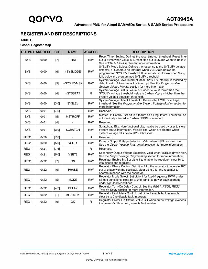
REGISTER AND BIT DESCRIPTIONS
Table 1:
Global Register Map
OUTPUT ADDRESS BIT NAME ACCESS DESCRIPTION
SYS 0x00 [7] TRST R/W Reset Timer Setting. Defines the reset time-out threshold. Reset time-out is 64ms when value is 1, reset time-out is 260ms when value is 0. See nRSTO Output section for more information.
SYS 0x00 [6] nSYSMODE R/W
SYSLEV Mode Select. Defines the response to the SYSLEV voltage detector, 1: Generate an interrupt when VVSYS falls below the programmed SYSLEV threshold, 0: automatic shutdown when VVSYS falls below the programmed SYSLEV threshold.
SYS 0x00 [5] nSYSLEVMSK R/W System Voltage Level Interrupt Mask. SYSLEV interrupt is masked by default, set to 1 to unmask this interrupt. See the Programmable System Voltage Monitor section for more information
SYS 0x00 [4] nSYSSTAT R System Voltage Status. Value is 1 when VVSYS is lower than the SYSLEV voltage threshold, value is 0 when VVSYS is higher than the system voltage detection threshold.
SYS 0x00 [3:0] SYSLEV R/W System Voltage Detect Threshold. Defines the SYSLEV voltage threshold. See the Programmable System Voltage Monitor section for more information.
SYS 0x01 [7:6] - R/W Reserved.
SYS 0x01 [5] MSTROFF R/W Master Off Control. Set bit to 1 to turn off all regulators. The bit will be automatically cleared to 0 when nPBIN is asserted.
SYS 0x01 [4] - R/W Reserved.
SYS 0x01 [3:0] SCRATCH R/W Scratchpad Bits. Non-functional bits, maybe be used by user to store system status information. Volatile bits, which are cleared when system voltage falls below UVLO threshold.
REG1 0x20 [7:6] - R Reserved.
REG1 0x20 [5:0] VSET1 R/W Primary Output Voltage Selection. Valid when VSEL is driven low. See the Output Voltage Programming section for more information.
REG1 0x21 [7:6] - R Reserved.
REG1 0x21 [5:0] VSET2 R/W Secondary Output Voltage Selection. Valid when VSEL is driven high. See the Output Voltage Programming section for more information.
REG1 0x22 [7] ON R/W Regulator Enable Bit. Set bit to 1 to enable the regulator, clear bit to 0 to disable the regulator.
REG1 0x22 [6] PHASE R/W Regulator Phase Control. Set bit to 1 for the regulator to operate 180° out of phase with the oscillator, clear bit to 0 for the regulator to operate in phase with the oscillator.
REG1 0x22 [5] MODE R/W Regulator Mode Select. Set bit to 1 for fixed-frequency PWM under all load conditions, clear bit to 0 to transit to power-savings mode under light-load conditions.
REG1 0x22 [4:2] DELAY R/W Regulator Turn-On Delay Control. See the REG1, REG2, REG3 Turn-on Delay section for more information.
REG1 0x22 [1] nFLTMSK R/W Regulator Fault Mask Control. Set bit to 1 enable fault-interrupts, clear bit to 0 to disable fault-interrupts.
REG1 0x22 [0] OK R Regulator Power-OK Status. Value is 1 when output voltage exceeds the power-OK threshold, value is 0 otherwise.

Data Sheet Rev. G, January 2020 | Subject to change without notice 12 of 46 www.qorvo.com
© 2020 Qorvo US, Inc. All rights reserved.
ACT8945A
Advanced PMU for Atmel SAMA5Dx Series & SAM9 Series Processors
REGISTER AND BIT DESCRIPTIONS CONT’D
OUTPUT ADDRESS BIT NAME ACCESS DESCRIPTION
REG2 0x30 [7:6] - R Reserved.
REG2 0x30 [5:0] VSET1 R/W Primary Output Voltage Selection. Valid when VSEL is driven low. See the Output Voltage Programming section for more information.
REG2 0x31 [7:6] - R Reserved.
REG2 0x31 [5:0] VSET2 R/W Secondary Output Voltage Selection. Valid when VSEL is driven high. See the Output Voltage Programming section for more information.
REG2 0x32 [7] ON R/W Regulator Enable Bit. Set bit to 1 to enable the regulator, clear bit to 0 to disable the regulator.
REG2 0x32 [6] PHASE R/W Regulator Phase Control. Set bit to 1 for the regulator to operate 180° out of phase with the oscillator, clear bit to 0 for the regulator to operate in phase with the oscillator.
REG2 0x32 [5] MODE R/W Regulator Mode Select. Set bit to 1 for fixed-frequency PWM under all load conditions, clear bit to 0 to transit to power- savings mode under light-load conditions.
REG2 0x32 [4:2] DELAY R/W Regulator Turn-On Delay Control. See the REG1, REG2, REG3 Turn-on Delay section for more information.
REG2 0x32 [1] nFLTMSK R/W Regulator Fault Mask Control. Set bit to 1 enable fault- interrupts, clear bit to 0 to disable fault-interrupts.
REG2 0x32 [0] OK R Regulator Power-OK Status. Value is 1 when output voltage exceeds the power-OK threshold, value is 0 otherwise.
REG3 0x40 [7:6] - R Reserved.
REG3 0x40 [5:0] VSET1 R/W Primary Output Voltage Selection. Valid when VSEL is driven low. See the Output Voltage Programming section for more information.
REG3 0x41 [7:6] - R Reserved.
REG3 0x41 [5:0] VSET2 R/W Secondary Output Voltage Selection. Valid when VSEL is driven high. See the Output Voltage Programming section for more information.
REG3 0x42 [7] ON R/W Regulator Enable Bit. Set bit to 1 to enable the regulator, clear bit to 0 to disable the regulator.
REG3 0x42 [6] - R/W Reserved.
REG3 0x42 [5] MODE R/W Regulator Mode Select. Set bit to 1 for fixed-frequency PWM under all load conditions, clear bit to 0 to transit to power- savings mode under light-load conditions.
REG3 0x42 [4:2] DELAY R/W Regulator Turn-On Delay Control. See the REG1, REG2, REG3 Turn-on Delay section for more information.
REG3 0x42 [1] nFLTMSK R/W Regulator Fault Mask Control. Set bit to 1 enable fault- interrupts, clear bit to 0 to disable fault-interrupts.
REG3 0x42 [0] OK R Regulator Power-OK Status. Value is 1 when output voltage exceeds the power-OK threshold, value is 0 otherwise.

Data Sheet Rev. G, January 2020 | Subject to change without notice 13 of 46 www.qorvo.com
© 2020 Qorvo US, Inc. All rights reserved.
ACT8945A
Advanced PMU for Atmel SAMA5Dx Series & SAM9 Series Processors
REGISTER AND BIT DESCRIPTIONS CONT’D
OUTPUT ADDRESS BIT NAME ACCESS DESCRIPTION
REG4 0x50 [7:6] - R Reserved.
REG4 0x50 [5:0] VSET R/W Output Voltage Selection. See the Output Voltage Programming section for more information.
REG4 0x51 [7] ON R/W Regulator Enable Bit. Set bit to 1 to enable the regulator, clear bit to 0 to disable the regulator.
REG4 0x51 [6] DIS R/W
Output Discharge Control. When activated, LDO output is discharged to GA through 1.5kΩ resistor when in shutdown. Set bit to 1 to enable output voltage discharge in shutdown, clear bit to 0 to disable this function.
REG4 0x51 [5] LOWIQ R/W LDO Low-IQ Mode Control. Set bit to 1 for low-power operating mode, clear bit to 0 for normal mode.
REG4 0x51 [4:2] DELAY R/W Regulator Turn-On Delay Control. See the REG4, REG5, REG6, REG7 Turn-on Delay section for more information.
REG4 0x51 [1] nFLTMSK R/W Regulator Fault Mask Control. Set bit to 1 enable fault- interrupts, clear bit to 0 to disable fault-interrupts.
REG4 0x51 [0] OK R Regulator Power-OK Status. Value is 1 when output voltage exceeds the power-OK threshold, value is 0 otherwise.
REG5 0x54 [7:6] - R Reserved.
REG5 0x54 [5:0] VSET R/W Output Voltage Selection. See the Output Voltage Programming section for more information.
REG5 0x55 [7] ON R/W Regulator Enable Bit. Set bit to 1 to enable the regulator, clear bit to 0 to disable the regulator.
REG5 0x55 [6] DIS R/W
Output Discharge Control. When activated, LDO output is discharged to GA through 1.5kΩ resistor when in shutdown. Set bit to 1 to enable output voltage discharge in shutdown, clear bit to 0 to disable this function.
REG5 0x55 [5] LOWIQ R/W LDO Low-IQ Mode Control. Set bit to 1 for low-power operating mode, clear bit to 0 for normal mode.
REG5 0x55 [4:2] DELAY R/W Regulator Turn-On Delay Control. See the REG4, REG5, REG6 , REG7 Turn-on Delay section for more information.
REG5 0x55 [1] nFLTMSK R/W Regulator Fault Mask Control. Set bit to 1 enable fault- interrupts, clear bit to 0 to disable fault-interrupts.
REG5 0x55 [0] OK R Regulator Power-OK Status. Value is 1 when output voltage exceeds the power-OK threshold, value is 0 otherwise.
REG6 0x60 [7:6] - R Reserved.
REG6 0x60 [5:0] VSET R/W Output Voltage Selection. See the Output Voltage Programming section for more information.
REG6 0x61 [7] ON R/W Regulator Enable Bit. Set bit to 1 to enable the regulator, clear bit to 0 to disable the regulator.
REG6 0x61 [6] DIS R/W
Output Discharge Control. When activated, LDO output is discharged to GA through 1.5kΩ resistor when in shutdown. Set bit to 1 to enable output voltage discharge in shutdown, clear bit to 0 to disable this function.
REG6 0x61 [5] LOWIQ R/W LDO Low-IQ Mode Control. Set bit to 1 for low-power operating mode, clear bit to 0 for normal mode.
REG6 0x61 [4:2] DELAY R/W Regulator Turn-On Delay Control. See the REG4, REG5, REG6, REG7 Turn-on Delay section for more information.
REG6 0x61 [1] nFLTMSK R/W Regulator Fault Mask Control. Set bit to 1 enable fault- interrupts, clear bit to 0 to disable fault-interrupts.

Data Sheet Rev. G, January 2020 | Subject to change without notice 14 of 46 www.qorvo.com
© 2020 Qorvo US, Inc. All rights reserved.
ACT8945A
Advanced PMU for Atmel SAMA5Dx Series & SAM9 Series Processors
REGISTER AND BIT DESCRIPTIONS CONT’D
OUTPUT ADDRESS BIT NAME ACCESS DESCRIPTION
REG6 0x61 [0] OK R Regulator Power-OK Status. Value is 1 when output voltage exceeds the power-OK threshold, value is 0 otherwise.
REG7 0x64 [7:6] - R Reserved.
REG7 0x64 [5:0] VSET R/W Output Voltage Selection. See the Output Voltage Programming section for more information.
REG7 0x65 [7] ON R/W Regulator Enable Bit. Set bit to 1 to enable the regulator, clear bit to 0 to disable the regulator.
REG7 0x65 [6] DIS R/W
Output Discharge Control. When activated, LDO output is discharged to GA through 1.5kΩ resistor when in shutdown. Set bit to 1 to enable output voltage discharge in shutdown, clear bit to 0 to disable this function.
REG7 0x65 [5] LOWIQ R/W LDO Low-IQ Mode Control. Set bit to 1 for low-power operating mode, clear bit to 0 for normal mode.
REG7 0x65 [4:2] DELAY R/W Regulator Turn-On Delay Control. See the REG4, REG5, REG6, REG7 Turn-on Delay section for more information.
REG7 0x65 [1] nFLTMSK R/W Regulator Fault Mask Control. Set bit to 1 enable fault- interrupts, clear bit to 0 to disable fault-interrupts.
REG7 0x65 [0] OK R Regulator Power-OK Status. Value is 1 when output voltage exceeds the power-OK threshold, value is 0 otherwise.
APCH 0x70 [7:0] - R/W Reserved.
APCH 0x71 [7] SUSCHG R/W Charge Suspend Control Input. Set bit to 1 to suspend charging, clear bit to 0 to allow charging to resume.
APCH 0x71 [6] - R/W Reserved.
APCH 0x71 [5:4] TOTTIMO R/W Total Charge Time-out Selection. See the Charge Safety Timers section for more information.
APCH 0x71 [3:2] PRETIMO R/W Precondition Charge Time-out Selection. See the Charge Safety Timers section for more information.
APCH 0x71 [1:0] OVPSET R/W Input Over-Voltage Protection Threshold Selection. See the Input Over-Voltage Protection section for more information.
APCH 0x78 [7] TIMRSTAT1 R/W
Charge Time-out Interrupt Status. Set this bit with TIMRPRE[ ] and/or TIMRTOT[ ] to 1 to generate an interrupt when charge safety timers expire, read this bit to get charge time-out interrupt status. See the Charge Safety Timers section for more information.
APCH 0x78 [6] TEMPSTAT1 R/W
Battery Temperature Interrupt Status. Set this bit with TEMPIN[ ] and/or TEMPOUT[ ] to 1 to generate an interrupt when a battery temperature event occurs, read this bit to get the battery temperature interrupt status. See the Battery Temperature Monitoring section for more information.
APCH 0x78 [5] INSTAT R/W
Input Voltage Interrupt Status. Set this bit with INCON[ ] and/or INDIS[ ] to generate an interrupt when UVLO or OVP condition occurs, read this bit to get the input voltage interrupt status. See the Charge Current Programming section for more information.
APCH 0x78 [4] CHGSTAT1 R/W
Charge State Interrupt Status. Set this bit with CHGEOCIN[ ] and/or CHGEOCOUT[ ] to 1 to generate an interrupt when the state machine gets in or out of EOC state, read this bit to get the charger state interrupt status. See the State Machine Interrupts section for more information.
APCH 0x78 [3] TIMRDAT1 R Charge Timer Status. Value is 1 when precondition time-out or total charge time-out occurs. Value is 0 in other case.
: Valid only when CHGIN UVLO Threshold< VCHGIN <CHGIN OVP Threshold.

Data Sheet Rev. G, January 2020 | Subject to change without notice 15 of 46 www.qorvo.com
© 2020 Qorvo US, Inc. All rights reserved.
ACT8945A
Advanced PMU for Atmel SAMA5Dx Series & SAM9 Series Processors
REGISTER AND BIT DESCRIPTIONS CONT’D
OUTPUT ADDRESS BIT NAME ACCESS DESCRIPTION
APCH 0x78 [2] TEMPDAT1 R Temperature Status. Value is 0 when battery temperature is outside of valid range. Value is 1 when battery temperature is inside of valid range.
APCH 0x78 [1] INDAT R Input Voltage Status. Value is 1 when a valid input at CHGIN is present. Value is 0 when a valid input at CHGIN is not present.
APCH 0x78 [0] CHGDAT1 R Charge State Machine Status. Value is 1 indicates the charger state machine is in EOC state, value is 0 indicates the charger state machine is in other states.
APCH 0x79 [7] TIMRTOT R/W
Total Charge Time-out Interrupt Control. Set both this bit and TIMRSTAT[ ] to 1 to generate an interrupt when a total charge time-out occurs. See the Charge Safety Timers section for more information.
APCH 0x79 [6] TEMPIN R/W
Battery Temperature Interrupt Control. Set both this bit and TEMPSTAT[ ] to 1 to generate an interrupt when the battery temperature goes into the valid range. See the Battery Temperature Monitoring section for more information.
APCH 0x79 [5] INCON R/W
Input Voltage Interrupt Control. Set both this bit and INSTAT[ ] to 1 to generate an interrupt when CHGIN input voltage goes into the valid range. See the Charge Current Programming section for more information.
APCH 0x79 [4] CHGEOCIN R/W Charge State Interrupt Control. Set both this bit and CHGSTAT[ ] to 1 to generate an interrupt when the state machine goes into the EOC state. See the State Machine Interrupts section for more information.
APCH 0x79 [3] TIMRPRE R/W
PRECHARGE Time-out Interrupt Control. Set both this bit and TIMRSTAT[ ] to 1 to generate an interrupt when a PRECHARGE time-out occurs. See the Charge Safety Timers section for more information.
APCH 0x79 [2] TEMPOUT R/W
Battery Temperature Interrupt Control. Set both this bit and TEMPSTAT[ ] to 1 to generate an interrupt when the battery temperature goes out of the valid range. See the Battery Temperature Monitoring section for more information.
APCH 0x79 [1] INDIS R/W
Input Voltage Interrupt Control. Set both this bit and INSTAT[ ] to 1 to generate an interrupt when CHGIN input voltage goes out of the valid range. See the Charge Current Programming section for more information.
APCH 0x79 [0] CHGEOCOUT R/W
Charge State Interrupt Control. Set both this bit and CHGSTAT[ ] to 1 to generate an interrupt when the state machines jumps out of the EOC state. See the State Machine Interrupts section for more information.
APCH 0x7A [7:6] - R Reserved.
APCH 0x7A [5:4] CSTATE R Charge State. Values indicate the current charging state. See the State Machine Interrupts section for more information.
APCH 0x7A [3:2] - R Reserved.
APCH 0x7A [1] ACINSTAT R
ACIN Status. Indicates the state of the ACIN input, typically in order to identify the type of input supply connected. Value is 1 when ACIN is above the 1.2V precision threshold, value is 0 when ACIN is below this threshold.
APCH 0x7A [0] - R Reserved.
: Valid only when CHGIN UVLO Threshold< VCHGIN <CHGIN OVP Threshold.

Data Sheet Rev. G, January 2020 | Subject to change without notice 16 of 46 www.qorvo.com
© 2020 Qorvo US, Inc. All rights reserved.
ACT8945A
Advanced PMU for Atmel SAMA5Dx Series & SAM9 Series Processors
SYSTEM CONTROL ELECTRICAL CHARACTERISTICS (VVSYS = 3.6V, TA = 25°C, unless otherwise specified.)
PARAMETER TEST CONDITIONS MIN TYP MAX UNIT
Input Voltage Range 2.7 5.5 V
UVLO Threshold Voltage VVSYS Rising 2.2 2.45 2.65 V
UVLO Hysteresis VVSYS Falling 200 mV
Supply Current
REG1, REG2, REG3, REG4, REG5, REG6 and REG7 Enabled. (PWM Mode)
14 mA
REG1, REG2, REG3, REG4, REG5, REG6 and REG7 Enabled. (PFM Mode, VIN = 3.6V)
420 µA
Shutdown Supply Current All Regulators Disabled 8 18 µA
Oscillator Frequency 1.8 2 2.2 MHz
Logic High Input Voltage1 1.4 V
Logic Low Input Voltage 0.4 V
Leakage Current VnIRQ = VnRSTO = 4.2V 1 µA
LBI Threshold Voltage VBAT Falling 1.03 1.2 1.31 V
LBI Hysteresis Threshold VBAT Rising 200 mV
Low Level Output Voltage2 ISINK = 5mA 0.35 V
nRSTO Delay 64 ms
PWRHLD Pull Down Resistor 500 kΩ
Thermal Shutdown Temperature Temperature rising 160 °C
Thermal Shutdown Hysteresis 20 °C
: PWRHLD, PWREN, VSEL are logic inputs.
2: nLBO, nPBSTAT, nIRQ, nRSTO are open drain outputs.
3: Typical value shown. Actual value may vary from (T-1ms) x 88% to T x 112%, where T = 64ms.

Data Sheet Rev. G, January 2020 | Subject to change without notice 17 of 46 www.qorvo.com
© 2020 Qorvo US, Inc. All rights reserved.
ACT8945A
Advanced PMU for Atmel SAMA5Dx Series & SAM9 Series Processors
STEP-DOWN DC/DC ELECTRICAL CHARACTERISTICS (VVP1 = VVP2 = VVP3 = 3.6V, TA = 25°C, unless otherwise specified.)
PARAMETER CONDITIONS MIN TYP MAX UNIT
Operating Voltage Range 2.7 5.5 V
UVLO Threshold Input Voltage Rising 2.5 2.6 2.7 V
UVLO Hysteresis Input Voltage Falling 100 mV
Quiescent Supply Current Regulator Enabled (PWM Mode) 4.5 mA
Regulator Enabled (PFM Mode) 65 µA
Shutdown Current VVP = 5.5V, Regulator Disabled 0 1 µA
Output Voltage Accuracy VOUT ≥ 1.2V, IOUT = 10mA -1% VNOM
1%
V VOUT < 1.2V, IOUT = 10mA -2% VNOM
2%
Line Regulation VVP = Max (VNOM1 +1, 3.2V) to 5.5V 0.15 %/V
Load Regulation IOUT = 10mA to IMAX2 0.0017 %/mA
Power Good Threshold VOUT Rising 93 %VNOM
Power Good Hysteresis VOUT Falling 2 %VNOM
Oscillator Frequency VOUT ≥ 20% of VNOM 1.8 2 2.2 MHz
VOUT = 0V 500 kHz
Soft-Start Period 400 µs
Minimum On-Time 75 ns
REG1
Maximum Output Current 1.1 A
Current Limit 1.55 1.80 2.05 A
PMOS On-Resistance ISW1 = -100mA 0.16 Ω
NMOS On-Resistance ISW1 = 100mA 0.16 Ω
SW1 Leakage Current VVP1 = 5.5V, VSW1 = 0 or 5.5V 0 1 µA
REG2
Maximum Output Current 1.1 A
Current Limit 1.55 1.80 2.05 A
PMOS On-Resistance ISW2 = -100mA 0.16 Ω
NMOS On-Resistance ISW2 = 100mA 0.16 Ω
SW2 Leakage Current VVP2 = 5.5V, VSW2 = 0 or 5.5V 0 1 µA
REG3
Maximum Output Current 1.2 A
Current Limit 1.55 1.80 2.05 A
PMOS On-Resistance ISW3 = -100mA 0.16 Ω
NMOS On-Resistance ISW3 = 100mA 0.16 Ω
SW3 Leakage Current VVP3 = 5.5V, VSW3 = 0 or 5.5V 0 1 µA
: VNOM refers to the nominal output voltage level for VOUT as defined by the Ordering Information section.
2: IMAX Maximum Output Current.

Data Sheet Rev. G, January 2020 | Subject to change without notice 18 of 46 www.qorvo.com
© 2020 Qorvo US, Inc. All rights reserved.
ACT8945A
Advanced PMU for Atmel SAMA5Dx Series & SAM9 Series Processors
LOW-NOISE LDO ELECTRICAL CHARACTERISTICS (VINL = 3.6V, COUT4 = COUT5 = COUT6 = COUT7 = 3.3µF, LOWIQ[ ] = [0], TA = 25°C, unless otherwise specified.)
PARAMETER TEST CONDITIONS MIN TYP MAX UNIT
Operating Voltage Range 2.5 5.5 V
Output Voltage Accuracy VOUT ≥ 1.2V, TA = 25°C, IOUT = 10mA -1% VNOM
2% V
VOUT < 1.2V, TA = 25°C, IOUT = 10mA -2% VNOM 4%
Line Regulation VINL = Max (VOUT + 0.5V, 3.6V) to 5.5V LOWIQ[ ] = [0] 0.05
mV/V VINL = Max (VOUT + 0.5V, 3.6V) to 5.5V LOWIQ[ ] = [1] 0.5
Load Regulation IOUT = 1mA to IMAX2 0.08 V/A
Power Supply Rejection Ratio f = 1kHz, IOUT = 20mA, VOUT =1.2V 75
dB f = 10kHz, IOUT = 20mA, VOUT =1.2V 65
Supply Current per Output
Regulator Enabled, LOWIQ[ ] = [0] 37 60
µA Regulator Enabled, LOWIQ[ ] = [1] 31 52
Regulator Disabled 0 1
Soft-Start Period VOUT = 2.9V 140 µs
Power Good Threshold VOUT Rising 89 %
Power Good Hysteresis VOUT Falling 3 %
Output Noise IOUT = 20mA, f = 10Hz to 100kHz, VOUT = 1.2V 50 µVRMS
Discharge Resistance LDO Disabled, DIS[ ] = 1 1.5 kΩ
REG4
Dropout Voltage IOUT = 80mA, VOUT > 3.1V 90 180 mV
Maximum Output Current 320 mA
Current Limit VOUT = 95% of regulation voltage 400 mA
Stable COUT4 Range 3.3 20 µF
REG5
Dropout Voltage IOUT = 80mA, VOUT > 3.1V 140 280 mV
Maximum Output Current 320 mA
Current Limit VOUT = 95% of regulation voltage 400 mA
Stable COUT5 Range 3.3 20 µF
REG6
Dropout Voltage IOUT = 80mA, VOUT > 3.1V 90 180 mV
Maximum Output Current 320 mA
Current Limit VOUT = 95% of regulation voltage 400 mA
Stable COUT6 Range 3.3 20 µF
REG7
Dropout Voltage IOUT = 80mA, VOUT > 3.1V 140 280 mV
Maximum Output Current 320 mA
Current Limit VOUT = 95% of regulation voltage 400 mA
Stable COUT7 Range 3.3 20 µF
: VNOM refers to the nominal output voltage level for VOUT as defined by the Ordering Information section.
2: IMAX Maximum Output Current.
3: Dropout Voltage is defined as the differential voltage between input and output when the output voltage drops 100mV below the regulation
voltage (for 3.1V output voltage or higher)
: LDO current limit is defined as the output current at which the output voltage drops to 95% of the respective regulation voltage.

Data Sheet Rev. G, January 2020 | Subject to change without notice 19 of 46 www.qorvo.com
© 2020 Qorvo US, Inc. All rights reserved.
ACT8945A
Advanced PMU for Atmel SAMA5Dx Series & SAM9 Series Processors
ActivePathTM CHARGER ELECTRICAL CHARACTERISTICS (VCHGIN = 5.0V, TA = 25°C, unless otherwise specified.)
PARAMETER TEST CONDITIONS MIN TYP MAX UNIT
ActivePath
CHGIN Operating Voltage Range 4.35 6.0 V
CHGIN UVLO Threshold CHGIN Voltage Rising 3.1 3.5 3.9 V
CHGIN UVLO Hysteresis CHGIN Voltage Falling 0.5 V
CHGIN OVP Threshold CHGIN Voltage Rising 6.0 6.6 7.2 V
CHGIN OVP Hysteresis CHGIN Voltage Falling 0.4 V
CHGIN Supply Current
VCHGIN < VUVLO 35 70 µA
VCHGIN < VBAT, + 50mV VCHGIN > VUVLO 100 200 µA
VCHGIN > VBAT + 150mV, VCHGIN > VUVLO
Charger disabled, IVSYS = 0mA 1.3 2.0 mA
CHGIN to VSYS On-Resistance IVSYS = 100mA 0.3 Ω
CHGIN to VSYS Current Limit
ACIN = VSYS 1.5 2 A
ACIN = GA, CHGLEV = GA 80 90 100 mA
ACIN = GA, CHGLEV = VSYS 400 450 500
VSYS REGULATION
VSYS Regulated Voltage IVSYS = 10mA 4.45 4.6 4.8 V
nSTAT OUTPUT
nSTAT Sink current VnSTAT = 2V 4 8 12 mA
nSTAT Leakage Current VnSTAT = 4.2V 1 µA
ACIN AND CHGLEV INPUTS
CHGLEV Logic High Input Voltage 1.4 V
CHGLEV Logic Low Input Voltage 0.4 V
CHGLEV Leakage Current VCHGLEV = 4.2V 1 µA
ACIN Voltage Thresholds ACIN voltage rising 1.03 1.2 1.31 V
ACIN Hysteresis Voltage ACIN voltage falling 200 mV
ACIN Leakage Current VACIN = 4.2V 1 µA
TH INPUT
TH Pull-Up Current VCHGIN > VBAT + 100Mv, Hysteresis = 50mV
91 102 110 µA
VTH Upper Temperature Voltage Threshold (VTHH) Hot Detect NTC Thermistor 0.47 0.50 0.53 V
VTH Lower Temperature Voltage Threshold (VTHL) Cold Detect NTC Thermistor 2.44 2.51 2.58 V
VTH Hysteresis Upper and Lower Thresholds 30 mV

Data Sheet Rev. G, January 2020 | Subject to change without notice 20 of 46 www.qorvo.com
© 2020 Qorvo US, Inc. All rights reserved.
ACT8945A
Advanced PMU for Atmel SAMA5Dx Series & SAM9 Series Processors
ActivePathTM CHARGER ELECTRICAL CHARACTERISTICS CONT’D (VCHGIN = 5.0V, TA = 25°C, unless otherwise specified.)
PARAMETER TEST CONDITIONS MIN TYP MAX UNIT
CHARGER
BAT Reverse Leakage Current VCHGIN = 0V, VBAT = 4.2V, IVSYS = 0mA 8 µA
BAT to VSYS On-Resistance 70 mΩ
ISET Pin Voltage Fast Charge 1.2
V Precondition 0.13
Charge Termination Voltage VTERM TA = -20°C to 70°C 4.179 4.2 4.221
V TA = -40°C to 85°C 4.170 4.2 4.230
Charge Current VBAT = 3.8V
RISET = 6.8K
ACIN = VSYS, CHGLEV = VSYS -10% ICHG1 +10%
mA ACIN = VSYS, CHGLEV = GA -10% ICHG/5 +10%
ACIN = GA, CHGLEV = VSYS 400 450 500
ACIN = GA, CHGLEV = GA 80 90 100
Precondition Charge Current VBAT = 2.7V
RISET = 6.8K
ACIN = VSYS, CHGLEV = VSYS 10% ICHG
mA ACIN = VSYS, CHGLEV = GA 10% ICHG
ACIN = GA, CHGLEV = VSYS 45
ACIN = GA, CHGLEV = GA 45
Precondition Threshold Voltage VBAT Voltage Rising 2.75 2.85 3.0 V
Precondition Threshold Hysteresis VBAT Voltage Falling 150 mV
END-OF-CHARGE Current Threshold
VBAT = 4.15V,
ACIN = VSYS, CHGLEV = VSYS 10% ICHG
mA ACIN = VSYS, CHGLEV = GA 10% ICHG
ACIN = GA, CHGLEV = VSYS 45
ACIN = GA, CHGLEV = GA 45
Charge Restart Threshold VTERM - VBAT, VBAT Falling 190 205 220 mV
Precondition Safety Timer PRETIMO[ ] = 10 80 min
Total Safety Timer TOTTIMO[ ] = 10 5 hr
Thermal Regulation Threshold 100 °C
: RISET (kΩ) = 2336 × (1V/ICHG (mA)) - 0.205

Data Sheet Rev. G, January 2020 | Subject to change without notice 21 of 46 www.qorvo.com
© 2020 Qorvo US, Inc. All rights reserved.
ACT8945A
Advanced PMU for Atmel SAMA5Dx Series & SAM9 Series Processors
TYPICAL PERFORMANCE CHARACTERISTICS (VVSYS = 3.6V, TA = 25°C, unless otherwise specified.)
Data Sheet Rev. G, January 2020 | Subject to change without notice 22 of 46 www.qorvo.com
© 2020 Qorvo US, Inc. All rights reserved.
ACT8945A
Advanced PMU for Atmel SAMA5Dx Series & SAM9 Series Processors
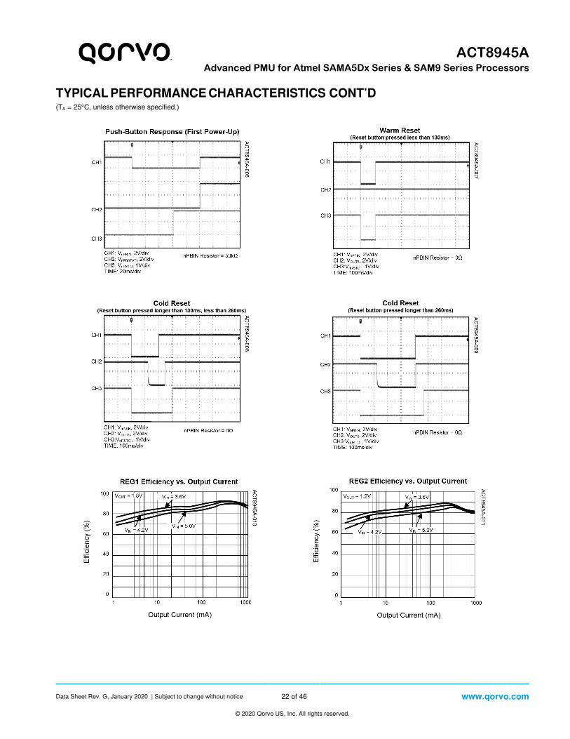
TYPICAL PERFORMANCE CHARACTERISTICS CONT’D (TA = 25°C, unless otherwise specified.)

Data Sheet Rev. G, January 2020 | Subject to change without notice 23 of 46 www.qorvo.com
© 2020 Qorvo US, Inc. All rights reserved.
ACT8945A
Advanced PMU for Atmel SAMA5Dx Series & SAM9 Series Processors
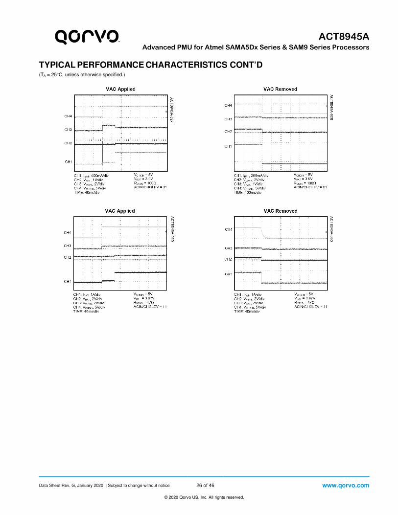
TYPICAL PERFORMANCE CHARACTERISTICS CONT’D (TA = 25°C, unless otherwise specified.)

Data Sheet Rev. G, January 2020 | Subject to change without notice 24 of 46 www.qorvo.com
© 2020 Qorvo US, Inc. All rights reserved.
ACT8945A
Advanced PMU for Atmel SAMA5Dx Series & SAM9 Series Processors
TYPICAL PERFORMANCE CHARACTERISTICS CONT’D (TA = 25°C, unless otherwise specified.)

Data Sheet Rev. G, January 2020 | Subject to change without notice 25 of 46 www.qorvo.com
© 2020 Qorvo US, Inc. All rights reserved.
ACT8945A
Advanced PMU for Atmel SAMA5Dx Series & SAM9 Series Processors
TYPICAL PERFORMANCE CHARACTERISTICS CONT’D (TA = 25°C, unless otherwise specified.)
Data Sheet Rev. G, January 2020 | Subject to change without notice 26 of 46 www.qorvo.com
© 2020 Qorvo US, Inc. All rights reserved.
ACT8945A
Advanced PMU for Atmel SAMA5Dx Series & SAM9 Series Processors
TYPICAL PERFORMANCE CHARACTERISTICS CONT’D (TA = 25°C, unless otherwise specified.)

Data Sheet Rev. G, January 2020 | Subject to change without notice 27 of 46 www.qorvo.com
© 2020 Qorvo US, Inc. All rights reserved.
ACT8945A
Advanced PMU for Atmel SAMA5Dx Series & SAM9 Series Processors
SYSTEM CONTROL INFORMATION
Interfacing with the Atmel SAMA5D3 Series & SAM9 Series Processors
The ACT8945A is optimized for use in applications using the following Atmel platforms: SAMA5D2, SAMA5D3, and
SAM9 series processors, supporting all the power domains as shown in the following table.
Table 2:
ACT8945A and Atmel SAMA5D2, SAMA5D3, and SAM9 Series Power Domains
POWER DOMAIN ACT8945A CHANNEL TYPE DEFAULT VOLTAGE CURRENT CAPABILITY
VDDIODDR/VDDCORE_LPDDR etc. REG1 DC/DC 1.8V / 1.5V / 1.35V 1100mA
VDDCORE_GBIT ENET, VDDIO_LPDDR etc.
REG2 DC/DC 1.2V / 1.0V 1100mA
VDDIOP, VDDOSC, VDDUTMII, VDDIOM,10/100 ENET etc.
REG3 DC/DC 3.3V 1200mA
VDDFUSE REG4 LDO 2.5V 320mA
VDDANA REG5 LDO 3.3V 320mA
Auxiliary 1 REG6 LDO 0.6V 320mA
Auxiliary 2 REG7 LDO 0.6V 320mA
: VOUT2 = 1.2V @ VSEL=0 (SAMA5 series) and VOUT2 = 1.0V @ VSEL=VIN (SAM9 series)

Data Sheet Rev. G, January 2020 | Subject to change without notice 28 of 46 www.qorvo.com
© 2020 Qorvo US, Inc. All rights reserved.
ACT8945A
Advanced PMU for Atmel SAMA5Dx Series & SAM9 Series Processors
SYSTEM CONTROL INFORMATION
Control Signals
Enable Inputs
The ACT8945A features a variety of control inputs,
which are used to enable and disable outputs
depending upon the desired mode of operation.
PWRHLD is a logic input, while nPBIN is a unique,
multi-function input.
nPBIN Multi-Function Input
ACT8945A features the nPBIN multi-function pin, which
combines system enable/disable control with a
hardware reset function. Select either of the two pin
functions by asserting this pin, either through a direct
connection to GA, or through a 50kΩ resistor to GA, as
shown in Figure 2.
Figure 2:
nPBIN Input
Warm/Cold Manual Reset Function
The second major function of the nPBIN input is to
provide warm and cold manual reset function. To
manually reset the processor, drive nPBIN directly to
GA through a low impedance (less than 2.5kΩ). An
internal timer detects the duration of the manual reset
event.
Short Press/Warm Reset
When the manual reset button is pressed for less than
130ms, ACT8945A commences a warm reset operation
where nRSTO immediately asserts low, then remains
asserted low until the manual reset button is released
for 64ms.
Long Press / Cold Reset (Power Cycle)
When the manual reset button is pressed for more than
130ms, ACT8945A commences a power cycle routine
in which case all regulators are turned off and then
turned back on after reset button is released with all the
registers reloaded to default values. When the
ACT8945A turns on again, it stays enabled for 128ms,
the PWRHLD need to be asserted during this time so
that the system remains powered, otherwise the
ACT8945A automatically shuts down.
nPBSTAT Output
nPBSTAT is an open-drain output that reflects the state
of the nPBIN input; nPBSTAT is asserted low whenever
nPBIN is asserted, and is high-Z otherwise. This output
is typically used as an interrupt signal to the processor,
to initiate a software-programmable routine such as
operating mode selection or to open a menu. Connect
nPBSTAT to an appropriate supply voltage (typically
OUT3) through a 10kΩ or greater resistor.
nRSTO Output
nRSTO is an open-drain output which asserts low upon
startup or when manual reset is asserted via the nPBIN
input. When asserted on startup, nRSTO remains low
until reset time-out period expires after OUT1 reaches
its power-OK threshold. When asserted due to manual-
reset, nRSTO immediately asserts low, then remains
asserted low until the nPBIN input is de-asserted and
the reset time-out period expires.
Connect a 10kΩ or greater pull-up resistor from nRSTO
to an appropriate voltage supply (typically OUT3).
nIRQ Output
nIRQ is an open-drain output that asserts low any time
an interrupt is generated. Connect a 10kΩ or greater
pull-up resistor from nIRQ to an appropriate voltage
supply. nIRQ is typically used to drive the interrupt input
of the system processor.
Many of the ACT8945A's functions support interrupt-
generation as a result of various conditions. These are
typically masked by default, but may be unmasked via
the I2C interface. For more information about the
available fault conditions, refer to the appropriate
sections of this datasheet.
Note that under some conditions a false interrupt may
be generated upon initial startup. For this reason, it is
recommended that the interrupt service routine check
and validate nSYSLEVMSK[ ] and nFLTMSK[ ] bits
before processing an interrupt generated by these bits.
These interrupts may be validated by nSYSSTAT[ ],
OK[ ] bits.

Data Sheet Rev. G, January 2020 | Subject to change without notice 29 of 46 www.qorvo.com
© 2020 Qorvo US, Inc. All rights reserved.
ACT8945A
Advanced PMU for Atmel SAMA5Dx Series & SAM9 Series Processors
Push-Button Control
The ACT8945A is designed to initiate a system enable
sequence when the nPBIN multi-function input is
asserted. Once this occurs, a power-on sequence
commences, as described below. The power-on
sequence must complete and the microprocessor must
take control (by asserting PWRHLD) before nPBIN is
de-asserted. If the microprocessor is unable to
complete its power-up routine successfully before the
user releases the push-button, the ACT8945A
automatically shuts the system down. This provides
protection against accidental or momentary assertions
of the push- button. If desired, longer “push-and-hold”
times can be implemented by simply adding an
additional time delay before asserting PWRHLD.
Control Sequences
The ACT8945A features a variety of control sequences
that are optimized for supporting system enable and
disable sequences of Atmel SAMA5D2 and SAMA5D3
series and SAM9 series application processors.
Enabling/Disabling Sequence
ACT8945AQJ305 Sequence
A typical enable sequence is initiated whenever the
following conditions occurs:
1) nPBIN is asserted low via 50KΩ resistance, or
2) A valid input voltage is present at CHGIN.
The enable sequence begins by enabling REG3/REG5.
When REG3/REG5 reaches its power-OK threshold,
nRSTO is asserted low, resetting the microprocessor.
When REG3/REG5 reaches its power-OK threshold for
2ms, REG1 is enabled. When REG3/REG5 reaches its
power-OK threshold for 4ms, REG2 is enabled. When
REG3/REG5 reaches its power-OK threshold for 8ms,
REG4 is enabled. When REG3 is above its power-OK
threshold when the reset timer expires, nRSTO is de-
asserted, allowing the microprocessor to begin its boot
sequence. REG6 and REG7 can be enabled or disabled
by PWREN after system powers up.
During the boot sequence, the microprocessor must
assert PWRHLD, holding the regulators to ensure that
the system remains powered after nPBIN is released.
As with the enable sequence, a typical disable
sequence is initiated when the user presses the push-
button, which interrupts the processor via the nPBSTAT
output. The actual disable sequence is completely
software-controlled, but typically involved initiating
various “clean-up” processes before finally set
MSTROFF[ ] bit to 1 to shut the system down.
Figure 3:
ACT8945AQJ305-T Enable/Disable Sequence
: Typical value shown, actual delay time may vary from (T-1ms) x 88% to T x 112%, where T is the typical delay time setting.

Data Sheet Rev. G, January 2020 | Subject to change without notice 30 of 46 www.qorvo.com
© 2020 Qorvo US, Inc. All rights reserved.
ACT8945A
Advanced PMU for Atmel SAMA5Dx Series & SAM9 Series Processors
FUNCTIONAL DESCRIPTION
I2C Interface
The ACT8945A features an I2C interface that allows
advanced programming capability to enhance overall
system performance. To ensure compatibility with a
wide range of system processors, the I2C interface
supports clock speeds of up to 400kHz (“Fast-Mode”
operation) and uses standard I2C commands. I2C
write-byte commands are used to program the
ACT8945A, and I2C read-byte commands are used to
read the ACT8945A’s internal registers. The
ACT8945A always operates as a slave device, and is
addressed using a 7-bit slave address followed by an
eighth bit, which indicates whether the transaction is a
read-operation or a write-operation, [1011011x].
SDA is a bi-directional data line and SCL is a clock
input. The master device initiates a transaction by
issuing a START condition, defined by SDA
transitioning from high to low while SCL is high. Data is
transferred in 8-bit packets, beginning with the MSB,
and is clocked-in on the rising edge of SCL. Each
packet of data is followed by an “Acknowledge” (ACK)
bit, used to confirm that the data was transmitted
successfully.
For more information regarding the I2C 2-wire serial
inter face, go to the NXP webs ite:
http://www.nxp.com.
Voltage Monitor and Interrupt
Programmable System Voltage Monitor
The ACT8945A features a programmable system-
voltage monitor, which monitors the voltage at VSYS
and compares it to a programmable threshold voltage.
The programmable voltage threshold is programmed by
SYSLEV[3:0], as shown in Table 4.
SYSLEV[ ] is set to 3.0V by default. There is a 200mV
rising hysteresis on SYSLEV[ ] threshold such that
VVSYS needs to be 3.2V(typ) or higher in order to
power up the IC.
The nSYSSTAT[ ] bit reflects the output of an internal
voltage comparator that monitors VVSYS relative to the
SYSLEV[ ] voltage threshold, the value of nSYSTAT[ ]
= 1 when VVSYS is lower than the SYSLEV[ ] voltage
threshold, and nSYSTAT[ ] = 0 when VVSYS is higher
than the SYSLEV[ ] voltage threshold. Note that the
SYSLEV[ ] voltage threshold is defined for falling
voltages, and that the comparator produces about
200mV of hysteresis at VSYS. As a result, once VVSYS
falls below the SYSLEV threshold, its voltage must
increase by more than about 200mV to clear that
condition.
After the IC is powered up, the ACT8945A responds in
one of two ways when the voltage at VSYS falls below
the SYSLEV[ ] voltage threshold:
1) If nSYSMODE[ ] = 1 (default case), when system
voltage level interrupt is unmasked (nSYSLEVMSK[
]=1) and VVSYS falls below the programmable threshold,
the ACT8945A asserts nIRQ, providing a software
“under-voltage alarm”. The response to this interrupt is
controlled by the CPU, but will typically initiate a
controlled shutdown sequence either or alert the user
that the battery is low. In this case the interrupt is
cleared when VVSYS rises up again above the SYSLEV
rising threshold and nSYSSTAT[ ] is read via I2C.
2) If nSYSMODE[ ] = 0, when VVSYS falls below the
programmable threshold the ACT8945A shuts down,
immediately disabling all regulators. This option is
useful for implementing a programmable “under- voltage
lockout” function that forces the system off when the
battery voltage falls below the SYSLEV threshold
voltage. Since this option does not support a controlled
shutdown sequence, it is generally used as a "fail-safe"
to shut the system down when the battery voltage is
too low.
Table 4:
SYSLEV Falling Threshold
SYSLEV[3:0] SYSLEV Falling Threshold
(Hysteresis = 200mV)
0000 2.3
0001 2.4
0010 2.5
0011 2.6
0100 2.7
0101 2.8
0110 2.9
0111 3.0
1000 3.1
1001 3.2
1010 3.3
1011 3.4
1100 3.5
1101 3.6
1110 3.7
1111 3.8
Data Sheet Rev. G, January 2020 | Subject to change without notice 31 of 46 www.qorvo.com
© 2020 Qorvo US, Inc. All rights reserved.
ACT8945A
Advanced PMU for Atmel SAMA5Dx Series & SAM9 Series Processors
Precision Voltage Detector
The LBI input connects to one input of a precision
voltage comparator, which can be used to monitor a
system voltage such as the battery voltage. An external
resistive-divider network can be used to set voltage
monitoring thresholds, as shown in Functional Block
Diagram. The output of the comparator is present at the
nLBO open-drain output.
Thermal Shutdown
The ACT8945A integrates thermal shutdown protection
circuitry to prevent damage resulting from excessive
thermal stress, as may be encountered under fault
conditions. This circuitry disables all regulators if the
ACT8945A die temperature exceeds 160°C, and
prevents the regulators from being enabled until the IC
temperature drops by 20°C (typ).
Data Sheet Rev. G, January 2020 | Subject to change without notice 32 of 46 www.qorvo.com
© 2020 Qorvo US, Inc. All rights reserved.
ACT8945A
Advanced PMU for Atmel SAMA5Dx Series & SAM9 Series Processors
STEP-DOWN DC/DC REGULATORS
General Description
The ACT8945A features three synchronous, fixed-
frequency, current-mode PWM step down converters
that achieve peak efficiencies of up to 97%. REG1 and
REG2 are capable of supplying up to 1100mA of output
current, while REG3 supports up to 1200mA. These
regulators operate with a fixed frequency of 2MHz,
minimizing noise in sensitive applications and allowing
the use of small external components.
100% Duty Cycle Operation
Each regulator is capable of operating at up to 100%
duty cycle. During 100% duty-cycle operation, the high-
side power MOSFET is held on continuously, providing
a direct connection from the input to the output (through
the inductor), ensuring the lowest possible dropout
voltage in battery powered applications.
Synchronous Rectification
REG1, REG2, and REG3 each feature integrated n-
channel synchronous rectifiers, maximizing efficiency
and minimizing the total solution size and cost by
eliminating the need for external rectifiers.
Soft-Start
When enabled, each output voltages tracks an internal
400μs soft-start ramp, minimizing input current during
startup and allowing each regulator to power up in a
smooth, monotonic manner that is independent of
output load conditions.
Compensation
Each buck regulator utilizes current-mode control and
a proprietary internal compensation scheme to
simultaneously simplify external component selection
and optimize transient performance over its full
operating range. No compensation design is required;
simply follow a few simple guidelines described below
when choosing external components.
Input Capacitor Selection
The input capacitor reduces peak currents and noise
induced upon the voltage source. A 4.7μF ceramic
capacitor is recommended for each regulator in most
applications.
Output Capacitor Selection
For most applications, 22μF ceramic output capacitors
are recommended for REG1, REG2 and REG3.
Despite the advantages of ceramic capacitors, care
must be taken during the design process to ensure
stable operation over the full operating voltage and
temperature range. Ceramic capacitors are available
in a variety of dielectrics, each of which exhibits
different characteristics that can greatly affect
performance over their temperature and voltage
ranges.
Two of the most common dielectrics are Y5V and
X5R. Whereas Y5V dielectrics are inexpensive and can
provide high capacitance in small packages, their
capacitance varies greatly over their voltage and
temperature ranges and are not recommended for
DC/DC applications. X5R and X7R dielectrics are
more suitable for output capacitor applications, as their
characteristics are more stable over their operating
ranges, and are highly recommended.
Inductor Selection
REG1, REG2, and REG3 utilize current-mode control
and a proprietary internal compensation scheme to
simultaneously simplify external component selection
and optimize transient performance over their full
operating range. These devices were optimized for
operation with 2.2μH inductors, although inductors in
the 1.5μH to 3.3μH range can be used. Choose an
inductor with a low DC-resistance, and avoid inductor
saturation by choosing inductors with DC ratings that
exceed the maximum output current by at least 30%.
Configuration Options
Output Voltage Programming
By default, each regulator powers up and regulates to
its default output voltage. Output voltage is selectable
by setting VSEL pin that when VSEL is low, output
voltage is programmed by VSET1[ ] bits, and when
VSEL is high, output voltage is programmed by VSET2[
] bits. However, once the system is enabled, each
regulator's output voltage may be independently
programmed to a different value, typically in order to
minimize the power consumption of the microprocessor
during some operating modes. Program the output
voltages via the I2C serial interface by writing to the
regulator's VSET1[ ] register if VSEL is low or VSET2
[ ] register if VSEL is high as shown in Table 5.
Enable / Disable Control
During normal operation, each buck may be enabled or
disabled via the I2C interface by writing to that
regulator's ON[ ] bit. The regulator accept rising or
falling edge of ON[ ] bit as on/off signal. To enable the
regulator, clear ON[ ] to 0 first then set to 1. To disable
the regulator, set ON[ ] to 1 first then clear it to 0.

Data Sheet Rev. G, January 2020 | Subject to change without notice 33 of 46 www.qorvo.com
© 2020 Qorvo US, Inc. All rights reserved.
ACT8945A
Advanced PMU for Atmel SAMA5Dx Series & SAM9 Series Processors
REG1, REG2, REG3 Turn-on Delay
Each of REG1, REG2 and REG3 features a
programmable Turn-on Delay which help ensure a
reliable qualification. This delay is programmed by
DELAY[2:0], as shown in Table 6.
Table 6:
REGx/DELAY[ ] Turn-On Delay
DELAY[2] DELAY[1] DELAY[0] TURN-ON DELAY(2)
0 0 0 0 ms
0 0 1 2 ms
0 1 0 4 ms
0 1 1 8 ms
1 0 0 16 ms
1 0 1 32 ms
1 1 0 64 ms
1 1 1 128 ms
Operating Mode
REG1, REG2, and REG3 each operate in fixed-
frequency PWM mode at medium to heavy loads when
MODE[ ] bit is set to 0, and transition to a proprietary
power-saving mode at light loads in order to maximize
standby battery life. In applications where low noise is
critical, force fixed-frequency PWM operation across
the entire load current range, at the expense of light-
load efficiency, by setting the MODE[ ] bit to 1.
OK[ ] and Output Fault Interrupt
Each DC/DC features a power-OK status bit that can be read by the system microprocessor via the I2C
interface. If an output voltage is lower than the power-OK threshold, typically 7% below the programmed regulation voltage, that regulator's OK[ ] bit will be 0. If a DC/DC's nFLTMSK[ ] bit is set to 1, the ACT8945A will interrupt the processor if that DC/DC's output voltage falls below the power-OK threshold. In this case, nIRQ will assert low and remain asserted until either the regulator is turned off or back in regulation, and the OK[ ] bit has been read via I2C.
PCB Layout Considerations
High switching frequencies and large peak currents
make PC board layout an important part of step-
down DC/DC converter design. A good design
minimizes excessive EMI on the feedback paths and
voltage gradients in the ground plane, both of which
can result in instability or regulation errors.
Step-down DC/DCs exhibit discontinuous input current,
so the input capacitors should be placed as close as
possible to the IC, and avoiding the use of via if
possible. The inductor, input filter capacitor, and
output filter capacitor should be connected as close
together as possible, with short, direct, and wide
traces. The ground nodes for each regulator's power
loop should be connected at a single point in a star-
ground configuration, and this point should be
connected to the backside ground plane with multiple
via. The output node for each regulator should be
connected to its corresponding OUTx pin through the
shortest possible route, while keeping sufficient
distance from switching nodes to prevent noise
injection. Finally, the exposed pad should be directly
connected to the backside ground plane using multiple
via to achieve low electrical and thermal resistance.

Data Sheet Rev. G, January 2020 | Subject to change without notice 34 of 46 www.qorvo.com
© 2020 Qorvo US, Inc. All rights reserved.
ACT8945A
Advanced PMU for Atmel SAMA5Dx Series & SAM9 Series Processors
Table 5:
REGx/VSET[ ] Output Voltage Setting
REGx/VSET[2:0] REGx/VSET[5:3]
000 001 010 011 100 101 110 111
000 0.600 0.800 1.000 1.200 1.600 2.000 2.400 3.200
001 0.625 0.825 1.025 1.250 1.650 2.050 2.500 3.300
010 0.650 0.850 1.050 1.300 1.700 2.100 2.600 3.400
011 0.675 0.875 1.075 1.350 1.750 2.150 2.700 3.500
100 0.700 0.900 1.100 1.400 1.800 2.200 2.800 3.600
101 0.725 0.925 1.125 1.450 1.850 2.250 2.900 3.700
110 0.750 0.950 1.150 1.500 1.900 2.300 3.000 3.800
111 0.775 0.975 1.175 1.550 1.950 2.350 3.100 3.900
Data Sheet Rev. G, January 2020 | Subject to change without notice 35 of 46 www.qorvo.com
© 2020 Qorvo US, Inc. All rights reserved.
ACT8945A
Advanced PMU for Atmel SAMA5Dx Series & SAM9 Series Processors
LOW-NOISE, LOW-DROPOUT LINEAR REGULATORS
General Description
REG4, REG5, REG6, and REG7 are low-noise, low-
dropout linear regulators (LDOs) that supply up to
320mA. Each LDO has been optimized to achieve low
noise and high-PSRR, achieving more than 65dB
PSRR at frequencies up to 10kHz.
Output Current Limit
Each LDO contains current-limit circuitry featuring a
current-limit fold-back function. During normal and
moderate overload conditions, the regulators can
support more than their rated output currents. During
extreme overload conditions, however, the current
limit is reduced by approximately 30%, reducing power
dissipation within the IC.
Compensation
The LDOs are internally compensated and require
very little design effort, simply select input and output
capacitors according to the guidelines below.
Input Capacitor Selection
Each LDO requires a small ceramic input capacitor to
supply current to support fast transients at the input
of the LDO. Bypassing each INL pin to GA with 1μF.
High quality ceramic capacitors such as X7R and X5R
dielectric types are strongly recommended.
Output Capacitor Selection
Each LDO requires a 3.3μF ceramic output capacitor
for stability. For best performance, each output
capacitor should be connected directly between the
output and GA pins, as close to the output as
possible, and with a short, direct connection. High
quality ceramic capacitors such as X7R and X5R
dielectric types are strongly recommended.
Configuration Options
Output Voltage Programming
By default, each LDO powers up and regulates to its
default output voltage. Once the system is enabled,
each output voltage may be independently programmed
to a different value by writing to the regulator's VSET[ ]
register via the I2C serial interface as shown in
Table 6.
Enable / Disable Control
During normal operation, each LDO may be enabled or
disabled via the I2C interface by writing to that LDO's
ON[ ] bit. The regulator accept rising or falling edge of
ON[ ] bit as on/off signal. To enable the regulator, clear
ON[ ] to 0 first then set to 1. To disable the regulator,
set ON[ ] to 1 first then clear it to 0.
REG4, REG5, REG6, REG7 Turn-on Delay
Each of REG4, REG5, REG6 and REG7 features a
programmable Turn-on Delay which help ensure a
reliable qualification. This delay is programmed by
DELAY[2:0], as shown in Table 6.
Output Discharge
Each of the ACT8945A’s LDOs features an optional
output discharge function, which discharges the output
to ground through a 1.5kΩ resistance when the LDO is
disabled. This feature may be enabled or disabled by
setting DIS[ ]; set DIS[ ] to 1 to enable this function, clear
DIS[ ] to 0 to disable it.
Low-Power Mode
Each of ACT8945A's LDOs features a LOWIQ[ ] bit
which, when set to 1, reduces the LDO's quiescent
current by about 16%, saving power and extending
battery lifetime.
OK[ ] and Output Fault Interrupt
Each LDO features a power-OK status bit that can be
read by the system microprocessor via the interface.
If an output voltage is lower than the power-OK
threshold, typically 11% below the programmed
regulation voltage, the value of that regulator's OK[ ]
bit will be 0.
If a LDO's nFLTMSK[ ] bit is set to 1, the ACT8945A
will interrupt the processor if that LDO's output voltage
falls below the power-OK threshold. In this case, nIRQ
will assert low and remain asserted until either the
regulator is turned off or back in regulation, and the
OK[ ] bit has been read via I2C.
PCB Layout Considerations
The ACT8945A’s LDOs provide good DC, AC, and
noise performance over a wide range of operating
conditions, and are relatively insensitive to layout
considerations. When designing a PCB, however,
careful layout is necessary to prevent other circuitry
from degrading LDO performance.
A good design places input and output capacitors as
close to the LDO inputs and output as possible, and
utilizes a star-ground configuration for all regulators
to prevent noise-coupling through ground. Output
traces should be routed to avoid close proximity to
noisy nodes, particularly the SW nodes of the DC/DCs.
REFBP is a noise-filtered reference, and internally has
a direct connection to the linear regulator controller.
Any noise injected onto REFBP will directly affect the

Data Sheet Rev. G, January 2020 | Subject to change without notice 36 of 46 www.qorvo.com
© 2020 Qorvo US, Inc. All rights reserved.
ACT8945A
Advanced PMU for Atmel SAMA5Dx Series & SAM9 Series Processors
outputs of the linear regulators, and therefore special
care should be taken to ensure that no noise is
injected to the outputs via REFBP. As with the LDO
output capacitors, the REFBP bypass capacitor should
be placed as close to the IC as possible, with short,
direct connections to the star-ground. Avoid the use of
via whenever possible. Noisy nodes, such as from the
DC/DCs, should be routed as far away from REFBP as
possible.

Data Sheet Rev. G, January 2020 | Subject to change without notice 37 of 46 www.qorvo.com
© 2020 Qorvo US, Inc. All rights reserved.
ACT8945A
Advanced PMU for Atmel SAMA5Dx Series & SAM9 Series Processors
ActivePathTM CHARGER
General Description
The ACT8945A features an advanced battery charger
that incorporates the patent-pending ActivePath
architecture for system power selection. This
combination of circuits provides a complete, advanced
battery-management system that automatically selects
the best available input supply, manages charge current
to ensure system power availability, and provides a
complete, high- accuracy (±0.5%), thermally regulated,
full-featured single-cell linear Li+ charger that can
withstand input voltages of up to 12V.
ActivePath Architecture
The ActivePath architecture performs three important
functions:
1) System Configuration Optimization
2) Input Protection
3) Battery-Management
System Configuration Optimization
The ActivePath circuitry monitors the state of the
input supply, the battery, and the system, and
automatically reconfigures itself to optimize the power
system. If a valid input supply is present, ActivePath
powers the system from the input while charging the
battery in parallel. This allows the battery to charge as
quickly as possible, while supplying the system. If a
valid input supply is not present, ActivePath powers the
system from the battery. Finally, if the input is present
and the system current requirement exceeds the
capability of the input supply, ActivePath allows system
power to be drawn from both the battery and the
input supply.
Input Protection
Input Over-Voltage Protection
The ActivePath circuitry features input over-voltage
protection circuitry. This circuitry disables charging
when the input voltage exceeds the voltage set by
OVPSET[ ] as shown in Table 7, but stands off the
input voltage in order to protect the system. Note that
the adjustable OVP threshold is intended to provide
the charge cycle with adjustable immunity against
upward voltage transients on the input, and is not
intended to allow continuous charging with input
voltages above the charger's normal operating voltage
range. Independent of the OVPSET[ ] setting, the
charge cycle is not allowed to resume until the input
voltage falls back into the charger's normal operating
voltage range (i.e. below 6.0V).
In an input over-voltage condition this circuit limits
VVSYS to 4.6V, protecting any circuitry connected to
VSYS from the over-voltage condition, which may
exceed this circuitry's voltage capability. This circuit is
capable of withstanding input voltages of up to 12V.
Table 7:
Input Over-Voltage Protection Setting
OVPSET[1] OVPSET[0] OVP THRESHOLD
0 0 6.6V
0 1 7.0V
1 0 7.5V
1 1 8.0V
Input Supply Overload Protection
The ActivePath circuitry monitors and limits the total
current drawn from the input supply to a value set by
the ACIN and CHGLEV inputs, as well as the resistor
connected to ISET. Drive ACIN to a logic- low for “USB
Mode”, which limits the input current to either 100mA,
when CHGLEV is driven to a logic- low, or 450mA,
when CHGLEV is driven to a logic- high. Drive ACIN to
a logic-high for “AC-Mode”, which limits the input current
to 2A, typically.
Input Under Voltage Lockout
If the input voltage applied to CHGIN falls below
3.5V (typ), an input under-voltage condition is
detected and the charger is disabled. Once an input
under-voltage condition is detected, a new charge
cycle will initiate when the input exceeds the under-
voltage threshold by at least 500mV.
Battery Management
The ACT8945A features a full-featured, intelligent
charger for Lithium-based cells, and was designed
specifically to provide a complete charging solution
with minimum system design effort.
The core of the charger is a CC/CV (Constant-
Current/Constant-Voltage), linear-mode charge
controller. This controller incorporates current and
voltage sense circuitry, an internal 70mΩ power
MOSFET, thermal-regulation circuitry, a full- featured
state machine that implements charge control and
safety features, and circuitry that eliminates the reverse
blocking diode required by conventional charger
designs.
The charge termination voltage is highly accurate
(±0.5%), and features a selection of charge safety
time-out periods that protect the system from
operation with damaged cells. Other features include
pin-programmable fast-charge current and one
current-limited nSTAT output that can directly drive
Data Sheet Rev. G, January 2020 | Subject to change without notice 38 of 46 www.qorvo.com
© 2020 Qorvo US, Inc. All rights reserved.
ACT8945A
Advanced PMU for Atmel SAMA5Dx Series & SAM9 Series Processors
LED indicator or provide a logic-level status signal to
the host microprocessor.
Dynamic Charge Current Control (DCCC)
The ACT8945A's ActivePath charger features dynamic charge current control (DCCC) circuitry, which acts to ensure that the system remains powered while operating within the maximum output capability of the power adapter. The DCCC circuitry continuously monitors VVSYS, and if the voltage at VSYS drops by
more than 200mV, the DCCC circuitry automatically reduces charge current in order to prevent VVSYS from
continuing to drop.
Charge Current Programming
The ACT8945A's ActivePath charger features a
flexible charge current-programming scheme that
combines the convenience of internal charge current
programming with the flexibility of resistor based
charge current programming. Current limits and charge
current programming are managed as a function of the
ACIN and CHGLEV pins, in combination with RISET, the
resistance connected to the ISET pin.
ACIN is a logic input that configures the current-limit of
ActivePath's linear regulator as well as that of the
battery charger. ACIN features a precise 1.2V logic
threshold, so that the input voltage detection threshold
may be adjusted with a simple resistive voltage
divider. This input also allows a simple, low- cost dual-
input charger switch to be implemented with just a
few, low-cost components.
When the voltage at ACIN is above the 1.2V
threshold, the charger operates in “AC-Mode” with a
charge current programmed by RISET, and the RISET is
given by:
RISET (kΩ) = 2336 × (1V/ICHG (mA)) - 0.205
With a given RISET then charge current will reduce 5
times when CHGLEV is driven low.
When ACIN is below the 1.2V threshold, the charger
operates in “USB-Mode”, with a maximum CHGIN
input current and charge current defined by the
CHGLEV input; 450mA, if CHGLEV is driven to a logic-
high, or 100mA, if CHGLEV is driven to a logic-low.
The ACT8945A's charge current settings are
summarized in Table 8.
Note that the actual charge current may be limited to
a current lower than the programmed fast charge
current due to the ACT8945A’s internal thermal
regulation loop. See the Thermal Regulation section for
more information.
Charger Input Interrupts
In order to ease input supply detection and eliminate
the size and cost of external detection circuitry, the
charger has the ability to generate interrupts based
upon the status of the input supply. This function is
capable of generating an interrupt when the input is
connected, disconnected, or both. An interrupt is
generated any time the input supply is connected when
INSTAT[ ] bit is set to 1 and the INCON[ ] bit is set to
1, and an interrupt is generated any time the input
supply is disconnected when INSTAT[ ] bit is set to 1
and the INDIS[ ] bit is set to 1.
INDAT[ ] indicates the status of the CHGIN input
supply. A value of 1 indicates that a valid CHGIN
input (CHGIN UVLO Threshold<VCHGIN<CHGIN OVP
Threshold) is present, a value of 0 indicates a valid
input is not present.
When an interrupt is generated by the input supply,
reading the INSTAT[ ] returns a value of 1. INSTAT
[ ] is automatically cleared to 0 upon reading. When
no interrupt is generated by the input supply, reading
the INSTAT[ ] returns a value of 0.
When responding to an Input Status Interrupt, it is
often useful to know the state of the ACIN input. For
example, in a dual-input charger application knowing
the state of the ACIN input can identify which type
of input supply has been connected. The state of the
ACIN input can be read at any time by reading the
ACINSTAT[ ] bit, where a value of 1 indicates that
the voltage at ACIN is above the 1.2V threshold
(indicating that a wall-cube has been attached), and a
value of 0 indicates that the voltage is below this
threshold (indicating that ACIN input is not valid and
USB supply input is selected).

Data Sheet Rev. G, January 2020 | Subject to change without notice 39 of 46 www.qorvo.com
© 2020 Qorvo US, Inc. All rights reserved.
ACT8945A
Advanced PMU for Atmel SAMA5Dx Series & SAM9 Series Processors
Table 8:
ACIN and CHGLEV Inputs
ACIN CHGLEV CHARGE CURRENT (mA) PRECONDITION CHARGE CURRENT (mA)
0 0 90 45
0 1 450 45
1 0 ICHG/5 10% × ICHG
1 1 ICHG 10% × ICHG

Data Sheet Rev. G, January 2020 | Subject to change without notice 40 of 46 www.qorvo.com
© 2020 Qorvo US, Inc. All rights reserved.
ACT8945A
Advanced PMU for Atmel SAMA5Dx Series & SAM9 Series Processors
Figure 5:
Typical Li+ charge profile and ACT8945A charge states
Figure 6:
Charger State Diagram

Data Sheet Rev. G, January 2020 | Subject to change without notice 41 of 46 www.qorvo.com
© 2020 Qorvo US, Inc. All rights reserved.
ACT8945A
Advanced PMU for Atmel SAMA5Dx Series & SAM9 Series Processors
Charge-Control State Machine
PRECONDITION State
A new charging cycle begins with the
PRECONDITION state, and operation continues in this
state until VBAT exceeds the Precondition Threshold
Voltage. When operating in PRECONDITION state,
the cell is charged at 10% of the programmed
maximum fast-charge constant current, ICHG.
Once VBAT reaches the Precondition Threshold Voltage,
the state machine jumps to the FAST- CHARGE state.
If VBAT does not reach the Precondition Threshold
Voltage before the Precondition Time-out period
expires, then the state machine jumps to the TIME-
OUT-FAULT state in order to prevent charging a
damaged cell. See the Charge Safety Timers section
for more information.
FAST-CHARGE State
In the FAST-CHARGE state, the charger operates in
constant-current (CC) mode and regulates the charge
current to the current set by RISET . Charging continues
in CC mode until VBAT reaches the charge termination
voltage (VTERM), at which point the state- machine jumps
to the TOP-OFF state. If VBAT does not reach VTERM
before the total time out period expires then the state-
machine will jump to the “EOC” state and will re-initiate
a new charge cycle after 32ms “relax”. See the Current
Limits and Charge Current Programming sections for
more information about setting the maximum charge
current.
TOP-OFF State
In the TOP-OFF state, the cell charges in constant-
voltage (CV) mode. In CV mode operation, the charger
regulates its output voltage to the 4.20V charge
termination voltage, and the charge current is naturally
reduced as the cell approaches full charge. Charging
continues until the charge current drops to END-OF-
CHARGE current threshold, at which point the state
machine jumps to the END- OF-CHARGE (EOC) state.
If the state-machine does not jump out of the TOP-
OFF state before the Total-Charge Time-out period
expires, then the state machine jumps to the EOC
state and will re-initiate a new charge cycle if VBAT falls
below termination voltage 205mV (typ). For more
information about the charge safety timers, see the
Charging Safety Times section.
END-OF-CHARGE (EOC) State
In the END-OF-CHARGE (EOC) state, the charger
presents a high-impedance to the battery, minimizing
battery current drain and allowing the cell to “relax”.
The charger continues to monitor the cell voltage, and
re-initiates a charging sequence if the cell voltage
drops to 205mV (typ) below the charge termination
voltage.
SUSPEND State
The state-machine jumps to the SUSPEND state any
time the battery is removed, and any time the input
voltage either falls below the CHGIN UVLO threshold
or exceeds the OVP threshold. Once none of these
conditions are present, a new charge cycle initiates.
A charging cycle may also be suspended manually by
setting the SUSPEND[ ] bit. In this case, initiate a new
charging sequence by clearing SUSPEND[ ] to 0.
State Machine Interrupts
The charger features the ability to generate interrupts
when the charger state machine transitions, based
upon the status of the CHG_ bits. Set CHGEOCIN[ ] bit
to 1 and CHGSTAT[ ] bit to 1 to generate an interrupt
when the charger state machine goes into the END-OF-
CHARGE (EOC) state. Set CHGEOCOUT[ ] bit to 1 and
CHGSTAT[ ] bit to 1 to generate an interrupt when the
charger state machine exits the EOC state.
CHGDAT[ ] indicates the status of the charger state
machine. A value of 1 indicates that the charger
state machine is in END-OF-CHARGE state, a value of
0 indicates the charger state machine is in other states.
When an interrupt is generated by the charger state
machine, reading the CHGSTAT[ ] returns a value of
1. CHGSTAT[ ] is automatically cleared to 0 upon
reading. When no interrupt is generated by the charger
state machine, reading the CHGSTAT[ ] returns a value
of 0.
For additional information about the charge cycle,
CSTATE[1:0] may be read at any time via I2C to
determine the current charging state.
Table 9:
Charging Status Indication
CSTATE[1] CSTATE[0] STATE MACHINE STATUS
1 1 PRECONDITION State
1 0 FAST-CHARGE/TOP-OFF State
0 1 END-OF-CHARGE State
0 0 SUSPEND/DISABLED/
FAULT State

Data Sheet Rev. G, January 2020 | Subject to change without notice 42 of 46 www.qorvo.com
© 2020 Qorvo US, Inc. All rights reserved.
ACT8945A
Advanced PMU for Atmel SAMA5Dx Series & SAM9 Series Processors
Thermal Regulation
The charger features an internal thermal regulation
loop that monitors die temperature and reduces
charging current as needed to ensure that the die
temperature does not exceed the thermal regulation
threshold of 110°C. This feature protects against
excessive junction temperature and makes the device
more accommodating to aggressive thermal designs.
Note, however, that attention to good thermal designs
is required to achieve the fastest possible charge time
by maximizing charge current.
Charge Safety Timers
The charger features programmable charge safety
timers which help ensure a safe charge by detecting
potentially damaged cells. These timers are
programmable via the PRETIMO[1:0] and
TOTTIMO[1:0] bits, as shown in Table 10 and Table 11.
Note that in order to account for reduced charge current
resulting from DCCC operation in thermal regulation
mode, the charge time-out periods are extended
proportionally to the reduction in charge current. As a
result, the actual safety period may exceed the
nominal timer period.
Charger Timer Interrupts
The charger features the ability to generate interrupts
based upon the status of the charge timers. Set the
TIMRPRE[ ] bit to 1 and TIMRSTAT[ ] bit to 1 to
generate an interrupt when the Precondition Timer
expires. Set the TIMRTOT[ ] bit to 1 and TIMRSTAT[
] bit to 1 to generate an interrupt when the Total-
Charge Timer expires.
TIMRDAT[ ] indicates the status of the charge timers.
A value of 1 indicates a precondition time- out or a
total charge time-out occurs, a value of 0 indicates
other cases.
When an interrupt is generated by the charge timers,
reading the TIMRSTAT[ ] returns a value of 1.
TIMRSTAT[ ] is automatically cleared to 0 upon
reading. When no interrupt is generated by the charge
timers, reading the TIMRSTAT[ ] returns a value of 0.
Table 10:
PRECONDITION Safety Timer Setting
PRETIMO[1]PRETIMO[0]PRECONDITION TIME-
OUT PERIOD
0 0 40 mins
0 1 60 mins
1 0 80 mins
1 1 Disabled
Table 11:
Total Safety Timer Setting
Charge Status Indicator
The charger provides a charge-status indicator output,
nSTAT. nSTAT is an open-drain output which sinks
current when the charger is in an active-charging
state, and is high-Z otherwise. nSTAT features an
internal 8mA current limit, and is capable of directly
driving a LED without the need of a current-limiting
resistor or other external circuitry. To drive an LED,
simply connect the LED between nSTAT pin and an
appropriate supply, such as VSYS. For a logic-level
charge status indication, simply connect a resistor from
nSTAT to an appropriate voltage supply.
Table 12:
Charging Status Indication
STATE nSTAT
PRECONDITION Active
FAST-CHARGE Active
TOP-OFF Active
END-OF-CHARGE High-Z
SUSPEND High-Z
TEMPERATURE FAULT High-Z
TIME-OUT-FAULT High-Z
Reverse-Current Protection
The charger includes internal reverse-current
protection circuitry that eliminates the need for
blocking diodes, reducing solution size and cost as well
as dropout voltage relative to conventional battery
chargers. When the voltage at CHGIN falls below VBAT,
the charger automatically reconfigures its power switch
to minimize current drawn from the battery.
Battery Temperature Monitoring
In a typical application, the TH pin is connected to the
battery pack's thermistor input, as shown in Figure 7.
The charger continuously monitors the temperature of
the battery pack by injecting a 102μA (typ) current into
the thermistor (via the TH pin) and sensing the voltage
at TH. The voltage at TH is continuously monitored,
and charging is suspended if the voltage at TH
exceeds either of the internal VTHH and VTHL thresholds
of 0.5V and 2.51V, respectively.
TOTTIMO[1] TOTTIMO[0] TOTAL TIME-OUT
PERIOD
0 0 3 hrs
0 1 4 hrs
1 0 5 hrs
1 1 Disabled

Data Sheet Rev. G, January 2020 | Subject to change without notice 43 of 46 www.qorvo.com
© 2020 Qorvo US, Inc. All rights reserved.
ACT8945A
Advanced PMU for Atmel SAMA5Dx Series & SAM9 Series Processors
The net resistance (from TH to GA) required to cross
the thresholds are given by:
102μA × RNOM × kHOT = 0.5V → RNOM × kHOT
≈ 5kΩ
102μA × RNOM × kCOLD = 2.51V → RNOM ×
kCOLD ≈ 25kΩ
where RNOM is the nominal thermistor resistance at
room temperature, and kHOT and kCOLD represent
the ratios of the thermistor's resistance at the desired
hot and cold thresholds, respectively, to the resistance
at 25°C.
Battery Temperature Interrupts
In order to ease detecting the status of the battery
temperature, the charger features the ability to
generate interrupts based upon the status of the
battery temperature. Set the TEMPOUT[ ] bit to 1 and
TEMPSTAT[ ] bit to 1 to generate an interrupt when
battery temperature goes out of the valid temperature
range. Set the TEMPIN[ ] bit to 1 and TEMPSTAT[ ]
bit to 1 to generate an interrupt when battery
temperature returns to the valid range.
TEMPDAT[ ] indicates the status of the battery
temperature. A value of 1 indicates the battery
temperature is inside of the valid range, a value of 0
indicates the battery is outside of the valid range.
When an interrupt is generated by the battery
temperature event, reading the TEMPSTAT[ ] returns a
value of 1. TEMPSTAT[ ] is automatically cleared to 0
upon reading. When no interrupt is generated by the
battery temperature event, reading the TEMPSTAT[ ]
returns a value of 0.
Figure 7:
Simple Configuration
Data Sheet Rev. G, January 2020 | Subject to change without notice 44 of 46 www.qorvo.com
© 2020 Qorvo US, Inc. All rights reserved.
ACT8945A
Advanced PMU for Atmel SAMA5Dx Series & SAM9 Series Processors
ERRATA INFO
Errata Name: ACT8945A creates I2C BUS contention
Device Identification: Parts marked
ACT8945AQJ305
Description:
The ACT8945A features an I2C interface that only
supports standard single-byte I2C command. After it detects a START condition, it will wait for its correct device address to issue the Acknowledge (ACK) by
pulling the SDA low. Therefore, if the ACT8945A I2C bus
shares with a multiple-byte I2C device, it would accidently issue an ACK once its address is detected and pull SDA low during mass data transmission between the MCU and the co-slave device. This action would
cause the I2C BUS to be frozen unexpectedly.
Recommendation:
To avoid the I2C BUS contention, we highly recommend customer to use ACT8945A I2C separately from a
multiple-byte I2C device such as a touch screen controller.
However, in case the ACT8945A has to share the I2C bus with a multiple-byte I2C device, the ACT8945A features a function to allow customer to disable its I2C interface to avoid the conflict.
Workaround:
For cases where ACT8945A I2C lines are already shared with some other components, ACT8945A
features a function to allow user to disable its I2C
interface to avoid conflicts. The following I2C write sequences perform this operation and configure SDA and SCL as high-Z pin.
Disable ACT8945AQJ305 I2C Interface
To disable the I2C interface of ACT8945AQJ305 and configure the SDA and SCL pins to input logic pins,
customer can use I2C to write the following commands in sequence below:
1. Write address 0x0B with 0xEE
2.Write address 0x02 with 0x07
3.Write address 0x03 with 0x01
4.Write address 0x0B with 0xEF
5.Write address 0x02 with 0x07
6.Write address 0x03 with 0x01

Data Sheet Rev. G, January 2020 | Subject to change without notice 45 of 46 www.qorvo.com
© 2020 Qorvo US, Inc. All rights reserved.
ACT8945A
Advanced PMU for Atmel SAMA5Dx Series & SAM9 Series Processors
PACKAGE OUTLINE AND DIMENSIONS
Top View Bottom View
Side View
Notes

Data Sheet Rev. G, January 2020 | Subject to change without notice 46 of 46 www.qorvo.com
© 2020 Qorvo US, Inc. All rights reserved.
ACT8945A
Advanced PMU for Atmel SAMA5Dx Series & SAM9 Series Processors
Important Notice
The information contained herein is believed to be reliable; however, Qorvo makes no warranties regarding the information contained
herein and assumes no responsibility or liability whatsoever for the use of the information contained herein. All information contained
herein is subject to change without notice. Customers should obtain and verify the latest relevant information before placing orders
for Qorvo products. The information contained herein or any use of such information does not grant, explicitly or implicitly, to any
party any patent rights, licenses, or any other intellectual property rights, whether with regard to such information itself or anything
described by such information. THIS INFORMATION DOES NOT CONSTITUTE A WARRANTY WITH RESPECT TO THE
PRODUCTS DESCRIBED HEREIN, AND QORVO HEREBY DISCLAIMS ANY AND ALL WARRANTIES WITH RESPECT TO
SUCH PRODUCTS WHETHER EXPRESS OR IMPLIED BY LAW, COURSE OF DEALING, COURSE OF PERFORMANCE,
USAGE OF TRADE OR OTHERWISE, INCLUDING THE IMPLIED WARRANTIES OF MERCHANTABILITY AND FITNESS FOR
A PARTICULAR PURPOSE.
Without limiting the generality of the foregoing, Qorvo products are not warranted or authorized for use as critical components in
medical, life-saving, or life-sustaining applications, or other applications where a failure would reasonably be expected to cause
severe personal injury or death.
Copyright 2019 © Qorvo, Inc. | Qorvo® and Active-Semi® are trademarks of Qorvo, Inc.
Product Compliance
This part complies with RoHS directive 2011/65/EU as amended by (EU) 2015/863.
This part also has the following attributes:
• Lead Free
• Halogen Free (Chlorine, Bromine)
Contact Information
For the latest specifications, additional product information, worldwide sales and distribution locations:
Web: www.qorvo.com Tel: 1-844-890-8163
Email: [email protected]
For technical questions and application information:
Email: [email protected]
Pb