
AC POWER LINE CARRIER COMMUNICATION - · PDF fileA PROJECT REPORT ON AC POWER LINE CARRIER...
64
A PROJECT REPORT ON AC POWER LINE CARRIER COMMUNICATION BY Dinesh Auti Nikhil Asawadekar Rohan Shroff Rohankumar Samal Under the guidance of Prof. Sachin Charbhe Submitted as a partial fulfillment of B.E.(Semester VIII), Electronics Engineering From RIZVI COLLEGE OF ENGINEERING BANDRA(W), MUMBAI - 400 050. UNIVERSITY OF MUMBAI. FOR THE ACADEMIC YEAR 2011-2012.
Transcript of AC POWER LINE CARRIER COMMUNICATION - · PDF fileA PROJECT REPORT ON AC POWER LINE CARRIER...

A PROJECT REPORT ON
AC POWER LINE CARRIER COMMUNICATION
BY
Dinesh AutiNikhil Asawadekar
Rohan ShroffRohankumar Samal
Under the guidance of
Prof. Sachin Charbhe
Submitted as a partial fulfillment of
B.E.(Semester VIII), Electronics EngineeringFrom
RIZVI COLLEGE OF ENGINEERINGBANDRA(W), MUMBAI - 400 050.
UNIVERSITY OF MUMBAI.FOR THE ACADEMIC YEAR 2011-2012.
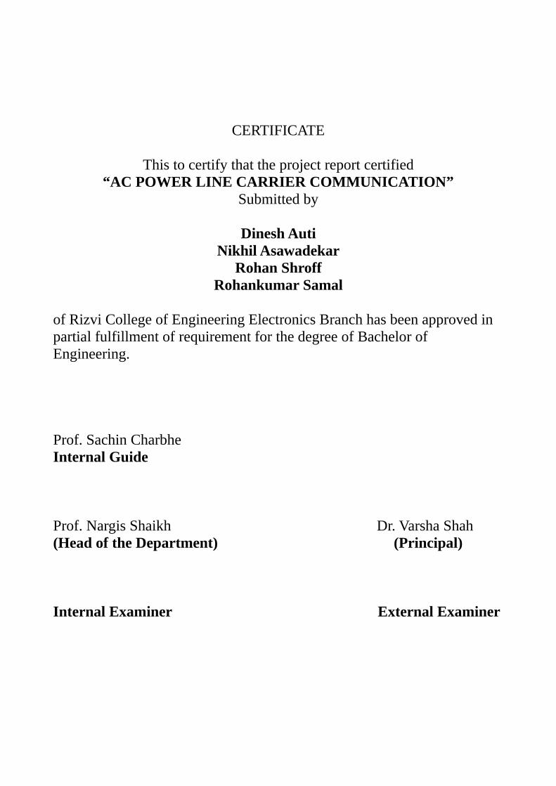
CERTIFICATE
This to certify that the project report certified“AC POWER LINE CARRIER COMMUNICATION”
Submitted by
Dinesh AutiNikhil Asawadekar
Rohan ShroffRohankumar Samal
of Rizvi College of Engineering Electronics Branch has been approved in partial fulfillment of requirement for the degree of Bachelor of Engineering.
Prof. Sachin CharbheInternal Guide
Prof. Nargis Shaikh Dr. Varsha Shah(Head of the Department) (Principal)
Internal Examiner External Examiner

ACKNOWLEDGEMENT
It is with great pleasure that we are submitting this report on “POWER LINE CARRIER
COMMUNICATION”. As in case project, we faced many problems while giving shape to
our ideas and making the project mold into reality.
We take this opportunity to express our sense of gratitude towards our internal guide Prof.
Sachin Charbhe for his valuable suggestions and guidance from time to time. We have
received constant support from Principal Prof. Varsha Shah, who has always encouraged
us to be innovative in our approach. We are also thankful to the head of department, Prof.
Nargis Shaikh and the remaining staff for making facilities available and giving their
support and guidance.
We express our sincere thanks to Prof. Ramkumar Maurya and Prof. Amit Redkar for
their apt advices and their valuable time that helped our project gain the desired form and
bring our ideas to reality. Guidance from Executive Engineer S.S.Lokare (MSEB, Airoli)
and Bhargav Thakkar (Technical Head at ABB Corporation) added to our conceptual
understanding of PLC systems.
Although we have not mentioned each name, we would like to say that we appreciate
every individual who was associated with our project and made experience satisfying and
fulfilling one.
iii

ABSTRACT
Our project aims at introducing an old technology in a new way. As an alternative to
existing communication systems. Traditional Power Line Communication (PLC) is
widely used to provide real-time communications for protection of high voltage
transmission lines. PLC is often the most economical and reliable high-speed dedicated
channel available for protective relaying. PLC system is mainly used for managing the
high voltage link and for communications between different substations.
Our project PLCC, Power Line Carrier Communication, is an approach to utilize the
existing power lines in the house or office for the transmission of information. Every
house and building has properly installed electricity lines. By using the existing AC
power lines as a medium to transfer the information, it becomes easy to connect the
houses with a high speed network access point without installing new wiring.
A power line carrier system includes three basic elements: a transmission line, presenting
a channel for the transmission of carrier signal between two communicating nodes.
Transformers and coupling equipment, providing a means of connection to the high-
voltage transmission line and to provide electrical isolation between power line and
circuitry. Transmitters and receivers circuitry . The simplified functional diagram of a
power line carrier system is shown and explained further in the report.
iv

List Of Figures
Name Of Figure Page No. Illustration No.
PLC Modem 7 1
PLC Modem Circuit 7 2
Block Diagram of PLCC 9 3
RGB VI Block Diagram 13 4
4RGB Front Panel 13 5
Hamming Code Encoder 14 6
G Matrix 15 7
G Matrix Front Panel 16 8
Hamming Code Encoder Output
16 9
XR 2206 Modulator 18 10
FSK Modulator Board Layout
18 11
Modulator Output (f1) 19 12
Modulator Output (f2) 19 13
Basic Coupling Circuit 20 14
Coupling Circuitry 21 15
Output (L=75%) 22 16
Output (L=25%) 22 17
Measuring Impedance Of Power Line
23 18
Impedance vs Frequency 24 19
Attenuation Measurement 24 20
Attenuation Survey 25 21
FSK Demodulator Schematics
29 22
FSK Demodulator Board Layout
29 23
Syndrome Matrix 32 24
Decoding Process 33 25
Parity Matrix 34 27
v

Parity Check Matrix 35 28
P and HT Matrix 35 29
Possible Error Patterns 36 30
Hamming Decoder 36 31
Original Message 37 32
Corrected Output 37 33
Transmitter Side 38 34
No Transmission Error 38 35
Single Bit Transmission Error
39 36
Two Bit Transmission Error 39 37
Multi Bit Transmission Error
39 38
vi

List Of Tables
Table Page No. Table No.
PLCC & Comparison 5 1
Syndrome Table 33 2
Modulator Components 43 3
Demodulator Components 44 4
Miscellaneous 44 5
vii

List Of Symbols & Abbreviations
Symbol Description
k Message bits
q Check Bits
n Code Word Length
M Message Vector
HT Parity Check Matrix
X Code Vector
Y Output Vector
G Generator Matrix
S Syndrome Vector
E Error Vector
C Check Bits Vector
RC Code Rate
IK (Identity Matrix) K * K
P Parity Matrix
SIndex Syndrome Index
CENELEC European Electro Technical Standards Committee
PLC Power Line Communication
PLCC Power Line Carrier Communication
PLL Phase Locked Loop
BPS Bits Per Seconds
ULP User Language Program
viii

Table of Contents
Acknowledgements........................................................................................................iii Abstract.........................................................................................................................iv List of figures.................................................................................................................v List of tables.................................................................................................................vii List of Symbols and abbreviations..............................................................................viii
1. Introduction............................................................................................................1
2. Literature Survey....................................................................................................22.1 PLCC Paper Analysis.......................................................................................22.2 Site Survey........................................................................................................4
3. Market Study.......................................................................................................... 53.1 Need According to Customer Point of View................................................... 5
3.1.1 Advantages Over Other Communication Systems............................63.2 Product Analysis & Study.................................................................................7
4. Block Diagram .........................................................................................................94.1 Block Description.............................................................................................10
5. Circuit Explanation................................................................................................12 5.1 Random bits generator......................................................................................12 5.2 Hamming Block Decoder.................................................................................14
5.3 Modulators........................................................................................................175.4 Coupling Circuitry............................................................................................205.5 Power line Characteristics................................................................................235.6 Receiver Side Coupling....................................................................................265.7 Demodulator.....................................................................................................275.8 Hamming Decoder............................................................................................30
6. Tools Used................................................................................................................406.1 Softwares used................................................................................................406.2 Hardware used................................................................................................44
7. Conclusion...............................................................................................................48
8. PLM v1.0 …............................................................................................................49
9. Applications............................................................................................................50
10. Future Scope.........................................................................................................53
11. References..............................................................................................................54
Index..............................................................................................................................55

Chapter 1 Introduction
1. Introduction
Data Transmission in the twentieth century mainly meant the transmission of
telephonic data over the wires. This had many disadvantages. Telephonic Equipment is
comparatively costlier. Telephone Circuits were often unreliable. Telephone Lines were
found to be unable to sustain the harsh weather conditions in the mountainous terrain and
the extreme weather. In addition the electrical interference between the parallel power
lines and the telephone lines was a case of concern. On the flip side the power Lines were
much more robust and reliable. Since power Lines were already available it made much
more sense to use them rather than investing in the making of new lines. Power Lines
Communication gained a lot of ground in the early twentieth century. The advantages
that were offered by the implementations of this technology and its social and economic
impacts led to many companies investing in this technology and using it in their own grid.
These Companies (GE, WestingHouse and much later AT&T) pioneered the development
of this technology. Today Data Transmission through Power Lines has covered a lot of
ground from its inception. It is available at a much lower cost and in a much compact
design.
1

Chapter 2 Literature Survey
2. Literature Survey
2.1 PLCC Paper Analysis
“ A Power Line Communication Tutorial - Challenges and Technologies ”
The Power Lines available today were built for the purpose of power transmission from
one place to another. The attempt to transmit data over these power lines leads to the
reception of a lot of noise. This noise is due to the numerous devices connected to the
power lines. An analysis of this noise and their characteristics helps us better understand
how to tackle the problem of noise elimination in the Power Lines. The characteristics of
the modulation techniques and their subsequent analysis gives us an idea of the
advantages and disadvantages of each technique. The receiver contains a phase locked
loop. We studied the modulation techniques and compared their performance in the
present of noise. Finally Spread Spectrum technology is reviewed for the use of
communications on Power Lines. Spread Spectrum is a method of signal modulation
where the transmitted signal occupies a bandwidth considerably higher than the minimum
necessary to send the information and some function other than the information being
sent is used to increase this Bandwidth. Spread Spectrum was found to be unsuitable and
rather detrimental for the PLCC system. Inference : After carefully studying the various
technology we infer that Digital Signal Processing is absolutely necessary for the system
to function efficiently. Spread Spectrum is found to be having a negative impact on the
output and hence should be avoided. FSK is found to be the most immune to noise and
hence chosen for our project.
2

Chapter 2 Literature Survey
“ Design Of Domestic Power Line Communication ”
This report discusses the power-line communication over the low-voltage grid, which has
A very high potential growth in the near future. The main advantage with power-line
communication is the use of an existing infrastructure. Wires exist to every household
connected to the power-line network. This report starts with a general introduction to
power line communication. Then it discusses the application of an existing home
automation system, then communicating over a low-voltage grid is investigated in order
to obtain some knowledge of how the power line acts as a communication channel. The
power-line communication channel can in general be modeled as a system with frequency
dependent signal-to-noise ratio varying with time over the communication bandwidth.
Finally we describe the basic parts of the system that eventually could be used for
information transfer over the power-line communication channel.
3

Chapter 2 Literature Survey
2.2 Site Survey
The best way to study any technology is to take guidance from the people who are
working in similar field. We came to know that Maharashtra State Electricity Board
(MSEB) and ABB Corporation are the two giants in the industry who use similar
technology. So our first step was to take help of technical experts working there in order
to tackle problems we are going to face.
We went to MSEB (Airoli) where Executive Engineer S.S.Lokare Sir helped us a lot to
make us aware of how PLCC actually works. He gave us examples of different sub-
stations situated near Navi-Mumbai & Mumbai area and explained us how actually power
flows from one sub-station to another via gantries and also how the main station situated
at Airoli controls everything. He also explained us how voice data travels through the
power line and showed us technical aspects of the same. He backed us for our project and
ensured that digital data can be made to flow over power line. By using modulation
techniques.
When we started struggling with coupling and isolation related problems we visited ABB
Corporation to take some help. We had surfed on the net that ABB works with PLCC
Technology. A visit to ABB was indeed of lot of help and support. Technical Head at ABB
Mr. Bhargav Thakkar helped us explaining how PLC Systems work on broader context.
He told us that for coupling purpose Current Voltage Transformer (CVT) which costs in
lakhs and is used to block the AC Power signal coming into the transmitter/receiver
system. Also we came to that Line Matching Unit (LMU) is used in PLCC which is used
to match the impedance of input and output circuitry and building prototype for it is not
possible. But he also ensured that for general prototype as a final year project a coupling
circuitry can be used instead. which consist of capacitors and inductors. This really
boosted our confidence and we started working accordingly.
4

Chapter 3 Market Study
3. Market Study
3.1 Need According to Customers Point of View
PLCC system in the market will have to compete against telephone and intercom
systems. PLCC system has the potential to outperform telephone and intercom systems.
As these systems require additional resources and installations. Which incur a lot of setup
cost. Plus the additional wiring makes system bulky and unportable. Whereas a power
line system does not incur any setup cost has no additional wiring and can perform rather
more efficiently than the conventional telephone and intercom systems. With the help of
PLCC system one can transmit and receive data as well as voice signals. PLCC is a plug
and play kind of system which can be plugged into any electric socket and
communication can be established within a same building or nearby areas. The customers
will be required to buy a PLCC system adapters which is a one time cost and can be used
for lifetime. Also the size of adapters is small which makes it easily portable unlike
telephone or intercom. So the user can take these adapters to a new place or new office
and the system is established within no time. All the user has to do is to plug the adapters
in sockets in the rooms he/she wants. Considering the above stated merits PLCC system
is certainly the best fit in today’s modern age. PLCC systems completely fit the need of
the customers as it eliminates the shortcomings of the conventional system. Now the only
concern according to customer point of view is the cost factor. Lets see the cost wise
analysis of PLCC system with telephone and intercom.
Intercom Telephone PLCC
Cost/unit( in Rs) 1650 500 + service tax* + installation charges
+ monthly rental
1350
Cost after one year/unit(in Rs.)
1650 12 X (service tax* + monthly rental)
1350
5

Chapter 3 Market Study
3.1.1 Advantages Over Other Communication Techniques
PLCC uses existing power line for communication so it provides many advantages over
traditionally used telephone models and other communication systems. The main
advantage of power line carrier communication is cost on infrastructure is reduced to a
large extent. Consider any building or company office as an example. To supply
electricity for the whole structure first Mains cables are dropped throughout the building
and it bears all the load thruster by fridge , fans and all the other equipments or devices
run on electricity. If PLCC modem is used in such an area , no additional wiring or
cabling is required as PLCC uses this power line only. Data is sent on this with
equipotential coupling circuitry using modulator and it's retrieved at the receiver's side
using demodulator. Thus elimination of wiring or cabling is the biggest bliss in
communication system. This is also a flexible type of service which can have different
formulations as per the need or application. Half duplex PLCC or Full Duplex PLCC
modems are available. Thus they are now greatly used in houses and small office
networks. It is also considered asx a replacement to intercom as it doesn't need any extra
cabling.The biggest relief to the customers is when you talk about installation charges and
service tax. Apart from initial installation charges , user doesn't need to pay service tax
and government taxes for it as he's using existing power line only for communication.
With built-in Error Checking and direct interface with uc as an ad-on , it's the biggest
source of Research and Development since last 50 years. With other applications like
Automatic meter reading , Fire & Security Alarm Systems and Lighting Control this
serves as the major Integration for all the tasks that can be computed easily. With the
invention of new modems such as PLC Modem from Sunrom Technologies , care has
been taken that though using a same platform for transmitter and receiver side , high
power side and low power side are isolated so chances of shock hazards are reduced to
large extent and device is made more user friendly.
6

Chapter 3 Market Study
3.2 Product Analysis
The successive step in study of PLCC is to have a glance on devices which are
using this technology. Technical Experts from ABB Corp and MSEB suggested us two
such devices mentioned below.
This device which supports Windows XP/Pro , Linux OS is like a home plug adapter in
the power line network for signal transmission, to achieve any power outlet next to
Internet . With data rate 200Mbps and working temperature range -20 to -60 degrees , this
serves as easy to connect, easy to use, plug and play device for home and small office
networking environment.
The above device has built-in on board AC isolated coupling circuit, which allows direct
and simple connections to mains. Due to isolation on AC part, there is no worry to get
7
Illustration 1: PLC Modem
Illustration 2: PLC Modem Circuit

Chapter 3 Market Study
shock on the low voltage side when working with it. So it's user friendly device. It has
high immunity to electrical noise persistence in the power line and built in error checking
so it never gives out corrupt data. It transmits and receives serial data at 9600 bps.
Transmission is based on byte by byte basis. Once you give one byte to module for
transmission, you will have to wait at least 500ms before a new byte is given to module
again since the module waits for zero crossing of AC mains to transfer a bit. For AC 50Hz
system the zero crossing of AC signals happens every 10ms and modem needs 50 zero
crossings to transmit one byte with error checking data. That is why it takes 500ms for
one byte. As a half duplex system it normally operates in Receiver mode , once your
application gives serial data to transmit on its RX-IN pin, it switches over to transmit and
transmits the data through power line. Due to low cost , built in error checking, it's mainly
used for Home Automation and Process Control.
8

Chapter 4 Block Diagram & Description
4. Block Diagram & Description
4.1 Block Diagram
9
Illustration 3: Block Diagram Of PLCC

Chapter 4 Block Diagram & Description
4.2 Block Diagram Description
This block diagram explanation will give the basic idea about the flow of data from
one user to another. It will give the general idea about the processing that the data
underwent from one section to another. Following is the end to end jest of the project. We
first generated a sequence of random bits with the use of Labview. This will act as the
data given by the user which is to be transmitted to the receiver. Random bits are
generated for illustration purpose. Random bits generator can generate bits form 4 bit to
as many bits desired. These random bits which is considered as data cannot be directly
sent over the power line because the data is bound to introduce an error due to noise
present on the power line. Noise on the line cannot be curbed but the error introduced can
be detected and corrected. For that Hamming codes are used which is capable of detecting
multiple errors but can correct multiple errors. In hamming code check bits are appended
at the end which will help the receiver to correct the error if any. Now we have a bit
stream of data and check bits. We need an interfacing device will will help us interface
the labview which is on the computer with the FSK modulator. That job is done by
arduino. Arduino takes the bit stream from the computer and generates the same bit
stream from one of its output pin. This stream of bits is now given to FSK modulator
which will convert the digital data to analog form so that it can be sent over a power line.
This is done because if digital data is sent over any channel then it will consume lot of
bandwidth and the signal will also get corrupted very easily. FSK modulator converts
logic 1 to sine wave of 2200Hz and logic 0 to sine wave of 1200Hz We have used XR
2206 as our FSK modulator. Now our information in in the frequency of the sine wave.
Noise on any channel affects frequency the least. So our data is safe But the power line is
of high voltage so care has to be taken so that the high voltage does not enter the
transmitter circuitry. For that coupling is done .Coupling provides the necessary isolation
between low and high voltage.
10

Chapter 4 Block Diagram & Description
The functioning of the receiver side blocks is the exact opposite as that of transmitter
side. The coupling circuitry on the receiver side not just provides the isolation but also
acts as a tuned circuit will allows only the high frequency in a selected band i.e. between
800Hz to 3000Hz to enter the receiver side. The FSK demodulator doe the exact opposite
of FSK modulator. It decodes the two frequencies into respective 1's and 0's. We have
used XR 2211 as or FSK demodulator. For the FSk demodulator to detect the input signal
it should be greater than 10mV. But not exceeding 3Vrms. Arduino is used for interfacing
the demodulator with the labview. The hamming decoder in Labview will detect and
correct error if any. by using the check bits. The hamming decoder can detect multiple
errors but correct only single bit errors. After the corrected code word is received the
decoder will remove the check bits so that the original data transmitted is extracted from
codeword and displayed.
11

Chapter 5 Circuit Explanation
5. Circuit Explanation
The PLCC system has been shown in the form of a block diagram representation in
illustration 3. The description below provides a flow of data from its origin to its
destination. Each block will be explained but importance will be given to its
implementation in the system above. First, let's take a look at the origin of data i.e.
possible sources of data and the form in which the data is available. The input to the
above system will be in the form of one's & zero's, so the analog counterpart needs to be
converted to its appropriate digital equivalent via suitable methods (not listed in the block
diagram). While doing so care has to taken that the baud rate must remain appropriate so
as to not violate the modulators design constraints.
Before starting it is assumed that the data at the input of the system is digital. Also
the code provided is graphical & is simulated in LabVIEW development environment.
Following is the block by block introduction to the system.
5.1 Random Bits Generator (RBG)
It is purely for simulation purposes that instead of giving any particular data, a
random bits stream is applied at the input of the system. It is based on the principle of
Bernoulli's noise. It generates a pseudo random sequence of one's & zero's depending on
the probability p, which is given as a input. For example if p=0.7 then there is a 70%
probability that the outcome of the Bernoulli's noise generator is 1.
P(X = i) = pi(1 – p)^(1 – i) (i = 0, 1)
Bernoulli noise is a special case of Binomial noise.
12

Chapter 5 Circuit Explanation
We will make a RBG in LabVIEW with the Bernoulli's noise VI (Virtual Instrument)
found in the Signal processing Toolkit. Below is the snapshot of the RBG.
The input to the Bernoulli's noise VI is the number of samples, which has a default
value of 128. The value of p is 0.5 (not shown). At the output a not equal to block is used
to convert the output of Bernoulli's noise to one's & zero's.
This the output snapshot of Bernoulli's noise showing a random bits pattern in
binary format. Now the output from the RBG is given to an Hamming coder, which will
provide the required noise immunity to our data. This is called as channel coding.
13
Illustration 4: RBG VI Block Diagram
Illustration 5: RBG Front Panel

Chapter 5 Circuit Explanation
5.2 Hamming Block Encoder
Hamming code is a type of linear block code. A block of data has 'k' message bits
and 'q' check bits. A random bits stream enters the hamming block encoder and output is
data packets each of size 'k+q'. This 'k+q' is denoted by 'n' and is called the block size.
Where,
n = 2q - 1 ; n>q
k = n - q
These codes have d min = 3, which means that they can detect up to two errors or correct
one single error. For example, if k=4 & q=3 then n =7. This represents a (7,4) hamming
code [6].
Code rate : It is defined as message length divided by code word length.
Code Rate = Rc = k/n ;
Higher the code rate is better and becomes more efficient
M = message vector = ( m1, m2, m3,....)1xk
C = check bits vector = ( c1, c2, c3,.......)1xq
X = Code vector = (M | C)1xn
14
Illustration 6: Hamming Code Encoder
Chapter 5 Circuit Explanation
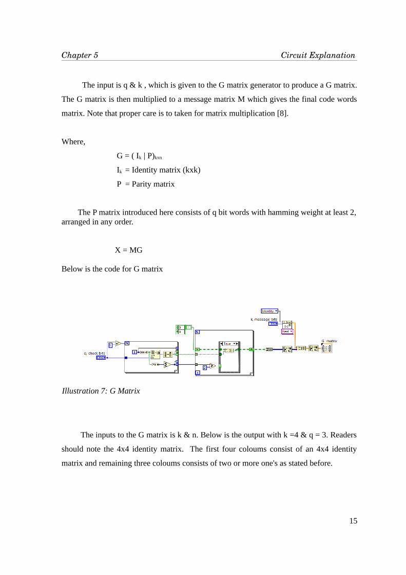
The input is q & k , which is given to the G matrix generator to produce a G matrix.
The G matrix is then multiplied to a message matrix M which gives the final code words
matrix. Note that proper care is to taken for matrix multiplication [8].
Where,
G = ( Ik | P)kxn
Ik = Identity matrix (kxk)
P = Parity matrix
The P matrix introduced here consists of q bit words with hamming weight at least 2, arranged in any order.
X = MG
Below is the code for G matrix
The inputs to the G matrix is k & n. Below is the output with k =4 & q = 3. Readers
should note the 4x4 identity matrix. The first four coloums consist of an 4x4 identity
matrix and remaining three coloums consists of two or more one's as stated before.
15
Illustration 7: G Matrix

Chapter 5 Circuit Explanation
Consider any one of the sixteen 4 bit messages Let's say M = (0110). Then for values of k
= 4 & q = 3, we get the following code word as shown in the snapshot below.
The important thing to note here is that the matrix multiplication between M & G is
a modulo 2 multiplication.
16
Illustration 8: G matrix Front Panel
Illustration 9: Hamming Code Encoder Output

Chapter 5 Circuit Explanation
5.3 Modulator
Let’s consider the Modulator. Modulation is the technique of forwarding low frequency
baseband signal to high frequency bandpass signal. The need of modulation here is to
mainly transform digital signal into equivalent analog signal using a form of modulation
known as Frequency Shift Keying (FSK). XR-2206 is a function generator IC which can
produce stabilized modulated FSK waveforms at frequencies ranging from 0.01 Hz to
1MHz.The XR-2206 is comprised of four functional blocks; a voltage-controlled
oscillator (VCO), an analog multiplier and sine-shaper; a unity gain buffer amplifier; and
a set of current switches. It offers output impedance in the range 600Ω + 10% .
The Mark and Space frequencies can be independently set by the choice of timing
resistors R1 and R2 respectively and the capacitor C0. So depending upon our
requirement we can select proper values of design variables [2]. C0 is chosen as 0.1uf and
from this we have evaluated the values needed for Mark and Space frequencies i.e R1 =
8.333KΩ and R2 = 4.545KΩ
17

Chapter 5 Circuit Explanation
Below is a schematic of the XR2206 Modulator from Exar.
The PCB Layout of the above modulator schematic is shown below.
18
Illustration 10: XR2206 Modulator
Illustration 11: FSK Modulator Board Layout

Chapter 5 Circuit Explanation
Output of the Modulator :
Following are the screen-shots of the DSO which was connected at the output of the
modulator.
19
Illustration 13: Modulator Output (f2)
Illustration12: Modulator output (f1)

Chapter 5 Circuit Explanation
5.4 Coupling Circuitry
A coupling circuit is used to connect the communication system to the power-line. The
purpose of the coupling circuits is two-fold. Firstly, it prevents the 50 Hz signal, used for
power distribution, to enter the equipment. Secondly, it certifies that the
receiver/transmitter circuit is tuned to work in a particular band of frequency. This
increases the efficiency of the receiver and makes sure that the receiver does not detect
any unwanted signal. The transformer in the coupling circuitry provides the necessary
impedance matching as well. The output of modulator which is a high frequency
bandpass signal is fed to the coupling circuitry which consist of transistor 2N2222 which
acts as a valve that allows only the high frequency modulated signal from the modulator
to reach the power line and block the 50Hz from entering the modulator circuitry. The
coupling circuit also incorporates a tank circuit which has a precharge capacitor so that
the oscillation amplitude remains steady. The frequency output of the tank circuit can be
tuned to a desired one by varying the inductor value of the slug-tuned IF(Intermediate
frequency ) transformer. The output frequency value depends upon the inductor and
capacitor value. The capacitors in series helps to attenuate the 50Hz signal and allow high
frequency from the tank circuit to pass through retaining its full strength [1].
20
Illustration 14: Basic Coupling Circuit

Chapter 5 Circuit Explanation
The circuit shown in illustration14 is explained above. The illustration below is a
snapshot of the simulation the coupling circuit. Illustration13 & 14 are the outputs of this
circuit for different values of inductor. The voltages and current at various nodes are
shown in the figure below.
21
Illustration 15: Coupling circuitry

Chapter 5 Circuit Explanation
Illustration 16 shows the condition when the value of the inductor is set to approximately 75% of its value. The attenuation of the sine wave for this value is negligible.
Illustration 17 shows the condition when the value of the inductor is set to approximately 25% of its value. The attenuation of the sine wave for this value is considerably satisfactory.
22
Illustration 16: Output (L = 75%)
Illustration 17: Output (L = 25%)

Chapter 5 Circuit Explanation
5.5 Power Line Characteristics
Impedance and attenuation measurements are performed on the loaded power lines
into three categories: rural, urban and the industrial power lines. Impedance of the power
lines looked at a wall receptacle in research building is measured by the circuit shown in
illustration 18. The frequency range of measurement is selected between 10 kHz and 150
kHz because these frequencies belong to the CENELEC bands. The measurements system
is described in illustration 18. A signal generator (SG) is used to simulate PLC carrier
signal and an AC millivoltmeter is used to measure the values of voltages: V1, V2 and V3
are shown in the circuit diagram. In the circuit, a coupling transformer T, and the coupling
capacitor C , are added to the measurements system because of this component should be
used on the PLC. Every modem must consist a coupling transformer and a coupling
capacitor to send or receive carrier from or to power lines. So, T and C are necessary
elements on the power line communications.
Power line impedance is a very important parameter on the design of power line
communications modem architecture. Variations on the impedance of the power line
affect the communications circuit performance. In order to determine impedance of the
power lines, measurements were carried out in Turkey at frequencies ranging from 10 to
170 kHz . Measurements were conducted in three categories: rural, urban and the
industrial power lines. The measured impedances were determined as 4-21 ohms for
urban. Here is a resonance and a local max at 60 kHz for urban power lines and
impedance of 4 to 12 ohms at 60-80 kHz bands at the urban power lines. After 80KHz the
impedance increases.
23
Illustration 18: Measuring Impedance of Power Line

Chapter 5 Circuit Explanation
Attenuation measurements are made using the hardware layout shown in illustration 20.
Two transceiver modems are used, one of them is a transmitter, the other one is the
receiver. T1 and C are the coupling transformer and coupling capacitor on the transmitter
modem and the others T2 and C are the same components on the receiver side. An AC
millivoltmeter is used to measure V1 and V2 voltages in order to calculate signal
attenuations on the along the power lines. Experiments on signal attenuations of the
power line are realized at different parts of homes. The parameters of the signal
attenuation measurements are line length, carrier frequency, the numbers of connector
box. The conductors of phase-neutral, phase-ground and neutral-ground may be used as
the communication channels. Normally phase-neutral conductors are used as PLC
channel, but in this study other ground conductor also observed. The reason of the
selection different channel ways is to examine the characteristics of the possible channels
in the PLC[7].
24
Illustration 19: Impedance vs Frequency

Chapter 5 Circuit Explanation
Phase-neutral power line channel in rural area has more attenuation with respect to other
phase- ground channels and neutral-ground channels up to frequencies 120 kHz, is shown
in illustration 21. Attenuation measurements in rural power lines are carried out at the
different plugs in the normally loaded homes. Selected homes are similar the each others
with about 120 m2. Attenuations are observed between 4-19 dB. Urban homes are
normally located at the city centers. Illustration 21 shows that power lines attenuations in
the urban decrease versus frequency after 70 kHz. Attenuation value may raise up to 23
dB in urban areas. Attenuation measurements at the all the different PLC channels such as
rural, urban and the industrial power lines are given in illustration 21 Measured o
attenuation values at the industrial power lines are bigger than rural and urban due to
heavy loads in this kind of power lines. These measurements are made inside homes
between different plugs on the wall, so line length is small such as a few ten meters.
These results may be used at the home automation modems via PLC.
25
Illustration 20: Attenuation Measurement
Illustration 21: Attenuation Survey

Chapter 5 Circuit Explanation
5.6 Receiver Side Coupling
Coupling at receiver side also performs the same job as that of transmitter side that to
block high voltage 50Hz and allow low voltage, high frequency carrier signal to pass
through. The circuitry and the role of the components in the circuit are exactly the same.
A coupling circuit is used to connect the communication system to the power-line. The
purpose of the coupling circuits is two-fold. Firstly, it prevents the 50 Hz signal, used for
power distribution, to enter the equipment. Secondly, it certifies that the
receiver/transmitter circuit is tuned to work in a particular band of frequency. This
increases the efficiency of the receiver and makes sure that the receiver does not detect
any unwanted signal. The transformer in the coupling circuitry provides the necessary
impedance matching as well.
The output of modulator which is a high frequency bandpass signal is fed to the coupling
circuitry which consist of transistor 2N2222 which acts as a valve that allows only the
high frequency modulated signal from the modulator to reach the power line and block
the 50Hz from entering the modulator circuitry. The coupling circuit also incorporates a
tank circuit which has a precharge capacitor so that the oscillation amplitude remains
steady. The frequency output of the tank circuit can be tuned to a desired one by varying
the inductor value of the slug-tuned IF(Intermediate frequency ) transformer. The output
frequency value depends upon the inductor and capacitor value. The capacitors in series
helps to attenuate the 50Hz signal and allow high frequency from the tank circuit to pass
through retaining its full strength.
26

Chapter 5 Circuit Explanation
Receiver Side :
The receiver side starts with a coupling to the power line. This is essential because
we need to separate low voltage circuit from high voltage power line. The coupling part
explained in the above section. After the coupling we need step down transformer to step
down the 230V voltage to 12V required by the receiver circuit to operate. Another main
reason for the transformer is to isolate the low power circuit from the high power circuit.
The low voltage step down signal is then passed to a tuned circuit, which will allow only
a select band of frequencies to pass. Arrangement for the above explanation is shown in
illustration 13. The signal that we get after the above step is then required to be
demodulated and then decoded. The demodulation is done using XR2211 FSK
DEMODULATOR from Exar Corporation. A hamming decoder is used to decode the
message.
Below is a block by block explanation of the receiver side.
5.7 Demodulator :
The XR -2211 is a Phase Locked Loop (PLL) integrated circuit especially designed
for data communication and particularly suited for FSK applications. It operates over a
frequency range of 0.01 Hz to 300KHz and can accommodate analog input signals
between 10mV(RMS) to 3V(RMS) [3]. Frequency shift keyed input signals fed into pin 2
of the XR-2211 must be capacitively coupled through a 0.1uf capacitor. The internal
impedance is 20K and the minimum recommended input signal is 10mV. The first order
of business is to set center frequency of the demodulator passband at the center of
frequency band that we wish to detect. For showing a prototype we have chosen center
frequency 1624 Hz. Mark frequency we have selected is 1200 Hz and space frequency is
2200 Hz. The center frequency of the two frequencies is 1624 Hz. The component values
are computed as follows.
27

Chapter 5 Circuit Explanation
f0 = 1/(R0*C0).
where R0 is 15.788K. The value of R0 is adjusted by using a 10K resistor and a variable
pot for fine adjustment. The value of C0 is chosen as 39nf. R1 sets the system bandwidth
and C1 states the loop filter time constant. and damping factor. The value of R1 is
determined by Mark and Space frequencies .
R1 = (R0*f0) / (f1-f2).
The value of C1 is chosen approximately as C0/4. The Resistor Rb provides positive
feedback across the fsk comparator and facilitates rapid transition between output logic
states. Cf and Rf form a single pole post detection filter for FSK data output. Rf is most
often set at 100K and Cf smooths the data output. Its value is roughly calculated [1].
Cf = 3/(Data Rate in Bits per second).
Because this modem is designed for operation at 1200 BPS , a value of 2.2nf is
acceptable.
28

Chapter 5 Circuit Explanation
The schematics of the XR2211 is show below.
Illustration 23 is the board layout of Demodulator using XR2211.
29
Illustration22: FSK Demodulator Schematics
Illustration 23: FSK Demodulator Board Layout

Chapter 5 Circuit Explanation
The output of the demodulator is in the form of ones & zeros. In order to read the values
of the demodulator we need a micro controller, which would properly interpret the
demodulators output so that it can be further processed & message can be decoded.
5.8 Hamming Decoder :
As shown below the generator matrix is used to generate a Code word from
message. If we use an ideal channel i.e. no transmission errors then the transmitted code
word should be equal to the received code word. But in reality this may not be the case.
There may be single bit or multiple bit errors. Errors are denoted by error vector E as
shown below. Error vector is the list of all possible error patterns that can be introduced
during transmission.
We know that the G matrix is represented as an augmentation of identity matrix and a
parity matrix as shown below
G = ( Ik | P)kxn
Ik = Identity matrix (kxk)
P = Parity matrix
30
Message
Error Vector
Received Code WordM X
E
Y
Code Word
G

Chapter 5 Circuit Explanation
The corresponding equivalent in the decoder is the Parity Check Matrix HT . The
parity check matrix is also a combination of an identity matrix and a parity matrix but
they are stacked one below the other as shown below
HT = ( P / Iq )n x q
One of the most important properties of the Parity Check Matrix HT is that modulo
2 multiplication of X and HT is always a zero vector. The only condition that is
required to be fulfilled is that X should be a valid code word.
Symbolically,
( HT )*( X ) = {0,0.........0}
This becomes the basis for error detection. In simple words if X is not a valid
codeword the product is going to be a non zero value.
We next define a matrix called as Syndrome Matrix denoted by 'S'
S = Y * ( HT )
Syndrome Vector is a 1/Q matrix.
Y is a 1/N matrix and H is N/Q matrix.
Consider Y = X+E
E = Vector of error patterns
X = Transmitted code word
Substituting value of Y in above equation , we get
S = (X+E) * ( HT )
S = X*( HT ) + E*( HT )
Note that addition in the above equation is Modulo2 addition.
31

Chapter 5 Circuit Explanation
From the above theory we know that X*( HT ) = 0.
Therefore S = E*( HT )
Suppose S = (00....) , this has two possible interpretations.
1. There are no transmission errors in the received codeword. Thus E = 0.
2. Occurrence of an undetectable transmission error that is Y appears to look like a
valid codeword.
Whenever S is not equal to zero , we say that error has been detected.
That error can be single bit error or multiple bit error.
Hamming code is a type of block code in which we can detect up to two bit errors
and correct upto one bit.
Since our syndrome has q bits , there are 2q possible syndromes and 2n possible error
patterns.
For eg. In our case ,
q = 3 for a (7,4) hamming code.
23 = 8 Syndrome patterns and 27 = 128 Error patterns.
Therefore we get 16 (128/8) , different errors produce the same syndrome.
That is not all errors can be corrected.
We adopt a procedure called as Maximum Likelihood Decoding wherein
1. 0 errors is most likely
2. Single bit error is next most likely.
We need to associate each possible syndrome with its most likely error pattern.
32
Illustration 24: Syndrome Matrix

Chapter 5 Circuit Explanation
In the above block diagram , we use the received codeword as the input in order to
calculate 'S'. Then we use a notation called as Syndrome Index Si which is used to point
to the suitable error pattern in the table of error pattern. The output of the table of error
patterns is E^. This E^ is our best possible guess of the position where the error has
occurred. Now we perform a modulo2 addition of E^ and the received codeword Y to get
the corrected code word X.
Syndrome (S) Error pattern (E)
000 0000 000
001 0000 001
010 0000 010
011 0010 000
100 0000 100
101 0100 000
110 1000 000
111 0001 000
Above table illustrates the Syndrome tables and the corresponding Error vector values.
33
Illustration 25: Decoding Process

Chapter 5 Circuit Explanation
Thus using concept of syndrome and the possible error vector values we are able to
correct the received code word which has up to single bit of error.
Following is a graphical code snapshot of the Parity Check Matrix HT .
As we can see in the illustration above we need the Parity Matrix as the input to
generate the parity check matrix. Consider the Parity matrix shown below
The parity matrix shown above consists of all the three bit values that contain one
or more than one 1's.
34
Illustration 26: Parity Check Matrix
Illustration 26: Parity Matrix

Chapter 5 Circuit Explanation
The parity check matrix is a (n x q) matrix as shown below. It is represented as
follows
HT = ( P / Iq )n x q
35
Illustration 28: Parity Check Matrix
Illustration 29: P and HT Matrix

Chapter 5 Circuit Explanation
List of all possible error patterns that can occur in a (7,4) hamming block code.
Figure below shows the entire decoder in a graphical form.
36
Illustration 31: Hamming Decoder
Illustration30: Possible Error patterns

Chapter 5 Circuit Explanation
Let's say that we send an encoded message shown in illustration 28 via the power line
towards the receiver. The encoded message consists of a 4-bit message and a 3-bit check
bit.
Below is an example of M = 0110 011.
Wherein,
m = 0110 ; message bits (4)
q = 011 ; Check bits (3)
The message that has been encoded i.e. m = 0110 is one of the valid sixteen
message words. Therefore if we assume a error free transmission then the output would
look like as shown in illustration 29.
If a error occurs during transmission then there may be following cases :
1. Single bit error transmission
2. Two bit error transmission
3. Multi bit error transmission
These cases are shown below
37
Illustration 32: Original Message
Illustration 33: Corrected Output

Chapter 5 Circuit Explanation
Transmitter side :
The illustration 30 shows the front panel of the transmitter side. The encoded bits section
shows the 7 bits that are to be transmitted serially out of the Power Line Communication
Modem. The figure also shows a boolean representation of the 7 bits encoded message.
The values of k, q and n are as shown in the illustration.
The value of n that is the codeword size depends upon the no. of check bits that are required. In our case, it's k = 4 , q = 3 and n = 7.
Receiver side :
1. No transmission error
38
Illustration 34: Tx side
Illustration 35: No transmission error

Chapter 5 Circuit Explanation
2. Single bit transmission error
3. Two bit transmission error
4. Multi bit transmission error
39
Illustration 36: Single bit transmission error
Illustration 37: Two bit transmission error
Illustration 38: Multi bit transmission error

Chapter 6 Tools Used
6. Tools Used
6.1 Softwares Used
1. NI LabVIEW
LabVIEW (short for Laboratory Virtual Instrumentation Engineering Workbench) is a
platform and development environment for a visual programming language from National
Instruments. The purpose of such programming is auto mating the usage of processing
and measuring equipment in any laboratory setup. LabVIEW is a graphical programming
environment used by engineers and scientists to develop sophisticated measurement, test,
and control systems using intuitive graphical icons and wires that resemble a flowchart. It
offers unrivaled integration with thousands of hardware devices and provides hundreds of
built-in libraries for advanced analysis and data visualization – all for creating virtual
instrumentation.
40
LabVIEW

Chapter 6 Tools Used
2. Eagle CAD
EAGLE provides quality PCB design software with the features that get the job done. For
over 20 years, EAGLE has been satisfying design engineers around the world, by offering
the same core functionality as expensive commercial software, at the fraction of the cost.
Easy to learn
•Schematic editor, layout editor, library editor modules with identical user interfaces
•Free service support through dedicated experts
•Compatible with Windows®, Linux®, Mac®
Easy to buy
•Purchase and license on-line or with personal support from our distributors
•No maintenance fees or add on contracts
Easy to use
•Flexible User Language Programs (ULPs) enable custom features, such as
individual instruction sequences, simulation, data export and import
•Export Gerber files that can be used at any board house:
•Gerber 274X & Gerber 274D
•Excellon NC Drill Format
•SM1000 and SM3000
•Custom user-defined export formats
•Online import of product & pricing information through DesignLink
•Active customer forums to share files, libraries ULPs, design tips and more
•Parse and paste your data outside of EAGLE (XM datastructure)
41
Chapter 6 Tools Used
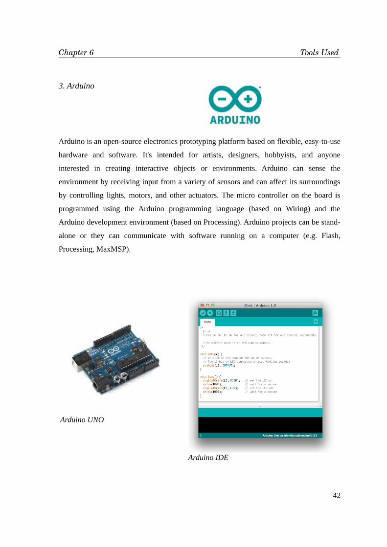
3. Arduino
Arduino is an open-source electronics prototyping platform based on flexible, easy-to-use
hardware and software. It's intended for artists, designers, hobbyists, and anyone
interested in creating interactive objects or environments. Arduino can sense the
environment by receiving input from a variety of sensors and can affect its surroundings
by controlling lights, motors, and other actuators. The micro controller on the board is
programmed using the Arduino programming language (based on Wiring) and the
Arduino development environment (based on Processing). Arduino projects can be stand-
alone or they can communicate with software running on a computer (e.g. Flash,
Processing, MaxMSP).
42
Arduino IDE
Arduino UNO

Chapter 6 Tools Used
4. MultiSim
NI Multisim (formerly MultiSIM) is an electronic schematic capture and simulation
program which is part of a suite of circuit design programs, along with NI Ultiboard.
Multisim is one of the few circuit design programs to employ the original Berkeley
SPICE based software simulation. Multisim was originally created by a company named
Electronics Workbench, which is now a division of National Instruments. Multisim
includes microcontroller simulation (formerly known as MultiMCU), as well as
integrated import and export features to the Printed Circuit Boardlayout software in the
suite, NI Ultiboard.
43

Chapter 6 Tools Used
6.2 Hardware Used
Modulator Components
Part Value Package Library Position(inch)
Orientation
C 10uF CPOL-R AD SparkFun (1.6.0.65) R180
C2 10uF CPOL-R AD SparkFun (2.05 1.75) R0
C3 1uF CPOL-R AD SparkFun (0.75 1.6) R90
C4 M01PTH_L CPOL-R AD SparkFun (0.85 0.75) R0
FSKIN M01PTH_L 1X01_L SparkFun (2.35 1.05) R90
FSKOUT M01PTH_L 1X01_L SparkFun (1.1 0.35) R0
Ground M01PTH_L 1X01_L SparkFun (2.35 1.45) R90
Ground 1 M01PTH_L 1X01_L SparkFun (0.5 0.35) R0
JP1 1X01_LS SparkFun (0.3 1.65) R90
R3 200 AXIAL_0.5 SparkFun (1.4 1.6) R0
R4 5.1K AXIAL_0.5 SparkFun (1.8 2.1) R0
R5 5.1K AXIAL_0.5 SparkFun (1.3 1.9) R0
U$1 TRIM_POT SparkFun (2.05 0.35) R90
U$2 TRIM_POT SparkFun (0.55 1.15) R180
U$3 TRIM_POT SparkFun (2.35 0.75) R180
u1 XR2206 DIL16 SparkFun (1.55 1.15) R0
Total Cost = Rs. 200
44

Chapter 6 Tools Used
Demodulator Components
Part Value Package Library Position(Inch)
Orientation
C 0.1uF CPOL_RAD SparkFun (1.1 1.9) R90
C0 27nF CPOL_RAD SparkFun (2 1.8) R90
C1 2.7nF CPOL_RAD SparkFun (2.2 0.4) R0
C2 0.1uF CPOL_RAD SparkFun (1 1.6) R0
C4 0.1uF CPOL_RAD SparkFun (2.6 1.6) R270
CF 1nF CPOL_RAD SparkFun (2.8 1.3) R270
DATAOUT MO1PTH_L 1x01_L SparkFun (0.8 0.5) R0
FSKIN MO1PTH_L 1x01_L SparkFun (0.4 0.8) R90
GND MO1PTH_L 1x01_L SparkFun (1.2 0.5) R0
GND2 MO1PTH_L 1x01_L SparkFun (0.4 1.3) R0
IC1 DIL14 SparkFun (1.55 1.5) R270
R0 5K 1% AXIAL-0.5 SparkFun (2.3 1.5) R90
R1 35.2K 1% AXIAL-0.5 SparkFun (2 1.1) R270
RB 510K AXIAL-0.5 SparkFun (1.5 0.8) R0
RF AXIAL-0.5 SparkFun (2.5 0.9) R180
RL 5.1K 1% AXIAL-0.5 SparkFun (0.7 1.6) R90
RX 20K TRIM_POT SparkFun (1.5 0.5) R0
SUPPLY 1X02_L SparkFun (2 2.2) R0
Total Cost = Rs.210
45
Chapter 6 Tools Used
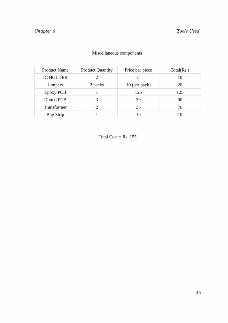
Miscellaneous components
Product Name Product Quantity Price per piece Total(Rs.)
IC HOLDER 2 5 10
Jumpers 2 packs 10 (per pack) 20
Epoxy PCB 1 125 125
Dotted PCB 3 30 90
Transformer 2 35 70
Bug Strip 1 10 10
Total Cost = Rs. 155
46
Chapter 6 Tools Used
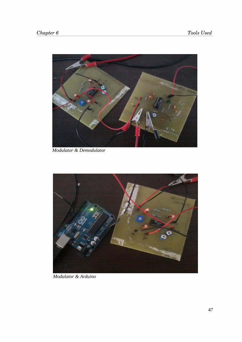
47
Modulator & Arduino
Modulator & Demodulator

Chapter 7 Conclusion
7. Conclusion
The project has the capability of transforming the information highway in India. In
a way that India has bypassed the land-line telephone revolution, the adaptation of PLCC
can help propel India into an elite group of countries with a very deep Internet
penetration. This would in turn help in dispelling the superstitions and ignorance that
prevails in some of the backward areas of the country. India’s image as a low cost
development country in the world would get a major boost by the implementation of this
technology on a wider scale. Power Lines Communication would result in a very large
scale savings of the tax payers money. Efficiency of the existing infrastructure would be
enhanced thus giving more value for money. It aims to ensure that the PLCC system can
be used as a plug and play device without any major investments on the part of the
consumer. PLCC is a technology that has the potential to revolutionize communication
and to change the lives of the citizens if factors such as cost, effectiveness and security
are carefully handled.
48

Chapter 8 PLM v1.0
8. PLM v1.0
Now as we have been through the practical and thesis sessions of this PLCC
project , our next aim is how to get it in compact form. As it includes many advantages
over other types of communication , it can be constructed or structured into compact form
or portable form. And yes , to get a PLC modem in compact or portable form is possible.
The duplex form of PLC is used now a days which allows the user to transmit and receive
the data from the same platform. This is the biggest revolution in PLCC technology as far
as communication over small houses , office networks and hub communication is
concerned. SMD components are used to build the circuitry which reduces circuit size
and weight of the product and thus restrictions over its portability can be eliminated. Built
in board AC connection circuits with direct connection to AC mains and built in carrier
generation technique can be used to reduce the external periferals which make the product
bulky. At the same time by using LEDs for transmission and receiption , built in error
checking can be implemented so correct data is guaranteed and it never gives corrupt
data. Also High Power circuitry and Low Power circuitry can be isolated on same PCB
thus serving both purposes less space, weight and hazard free device. AC isolated
coupling circuit, allows direct and simple connections to mains. Due to isolation on AC
part, there is no worry to get shock on the low voltage side when working with it. The
total cost of the entire trans-receiver unit does not exceed Rs.1500. Thus an economical
solution has been provided for data communication via PLCC modem by this project.
49
Chapter 9 Applications
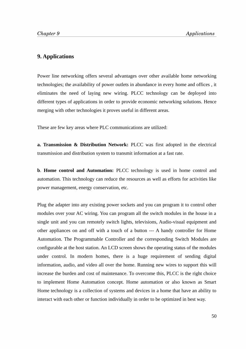
9. Applications
Power line networking offers several advantages over other available home networking
technologies; the availability of power outlets in abundance in every home and offices , it
eliminates the need of laying new wiring. PLCC technology can be deployed into
different types of applications in order to provide economic networking solutions. Hence
merging with other technologies it proves useful in different areas.
These are few key areas where PLC communications are utilized:
a. Transmission & Distribution Network: PLCC was first adopted in the electrical
transmission and distribution system to transmit information at a fast rate.
b. Home control and Automation: PLCC technology is used in home control and
automation. This technology can reduce the resources as well as efforts for activities like
power management, energy conservation, etc.
Plug the adapter into any existing power sockets and you can program it to control other
modules over your AC wiring. You can program all the switch modules in the house in a
single unit and you can remotely switch lights, televisions, Audio-visual equipment and
other appliances on and off with a touch of a button --- A handy controller for Home
Automation. The Programmable Controller and the corresponding Switch Modules are
configurable at the host station. An LCD screen shows the operating status of the modules
under control. In modern homes, there is a huge requirement of sending digital
information, audio, and video all over the home. Running new wires to support this will
increase the burden and cost of maintenance. To overcome this, PLCC is the right choice
to implement Home Automation concept. Home automation or also known as Smart
Home technology is a collection of systems and devices in a home that have an ability to
interact with each other or function individually in order to be optimized in best way.
50

Chapter 9 Applications
Using PLCC technology, existing power wiring of the house is used to connect home
appliances with each other as well as with Internet. Architecture of a PLCC based home
automation system is shown in the above image. Various home appliances are connected
within a loop through the existing power cables. This technology can connect each device
with the network which is connected to an AC outlet. All appliances are also connected
with a centralized control panel which controls them.
c. Entertainment: PLCC is used to distribute the multimedia content throughout the
home.
d. Telecommunication: Data transmission for different types of communications like
telephonic communication, audio, video communication can be made with the use of
PLCC technology.
e. Security Systems: In monitoring houses or businesses through surveillance cameras,
PLCC technology is far useful. The surveillance cameras connected over Power System
in a light bulb is unique; simply screw it into any light socket. Hidden inside the "bulb" is
a sophisticated Low-Light Monochrome Camera, coupled with PLCC circuitry. The video
signal is "encoded" by this circuit and fed directly to the power line. Each Video Over
Power System features a companion Decoder, which plugs into any wall outlet. A typical
homeowner would plug in the decoder at the outlet nearest the TV. A standard video
output connects the decoder to any TV or VCR using line-level RCA-type cables.
51

Chapter 9 Applications
Once the Decoder is plugged in and connected, live video is delivered to the TV or VCR.
It's simple and easy. There are no wires to run, no holes to drill, and no antennas or
complicated "tuning" is required.
f. Automatic Meter Reading : Automatic Meter reading applications use the PLCC
technology to send the data from home meters to Host Central Station. Automatic Meter
Reading using PLCC technology is quite useful as it saves a lot of human efforts and also
makes the whole system more efficient. The automatic meter reading system consists of
three components, namely, Multifunction Node (MFN), Concentrator & Communication
Node (CCN) and Operation & Management System (OMS). Different components and
their inter-connections are shown in the figure.
MFN is a unit installed in household meters, either incorporated in the meter itself or
externally connected to it. Its function is to take reading of the meter on an hourly basis
and store it in a memory chip. CNN is another part which manages all MFNs within a
particular area and collects meter readings from all MFNs. It is generally installed on
substations and needs a computer. The computer is installed with Operation and
Management System (OMS) which further manages all the data and meter readings from
CNNs.
52

Chapter 10 Future Scope
10. Future Scope
a. Telecommunication: Data transmission for different types of communications like
telephonic communication, audio, video communication can be made with the use of
PLCC technology. The user will be free to choose the necessary mode of communication.
b. Industrial Automation: In an industrial environment the PLC communication
networks can be used to give electric energy related services, such as meter reading,
demand management and remote billing but also to give value added services like remote
control and security, automation or even, education, information and e business
opportunities. On the other hand it can also offer telecommunication services such as
traditional telephony and Internet.
c. System protection: The communication link can be used to transit control signals that
may be used to protect the system. For example, PLC can be successfully used in order to
detect is landing operation of DER units.
d. Telecommunication services: Current PLC networks are able to reach speeds of
200Mbps. Telephony and Internet services can be delivered at high speed through
broadband PLC networks. Traditional telephony uses Plesiochronous Digital Hierarchy,
PDH. PDH uses Time Division Multiplexing, TDM. One possibility is to send the TDM
frame over IP, and the voice over TDM, VoTDM. However, this service should
accomplish the quality and reliability criteria, like Bit Error Rate, timing and latency, and
unfortunately the delay in VoTDM transmissions exceeds 25ms. Nevertheless, it is
possible to give a good telephony service over IP. Over TCP/IP, VoIP and Internet
services can be delivered at a 200Mbps speed, so it can be possible to compete with
technologies such as ADSL.
53

Chapter 11 References
11. References
[1] Ciarcia's Circuit Cellar, Volume 7
Build a Power-Line Carrier Current modem.
[2] Designing Reliable Powerline Communications Published in EDN
Ashish Garg and Angad Singh Gill, Cypress Semiconductor -- EDN, Dec 2, 2010
[3] Power Line Communication Modem
Power Line Communication Modem Solutions from Texas Instruments
[4] Data communication and networking - Behrouz A Forouzan.
Hamming Code - page 280.
[5] Measurements and attenuation for power line communication systems.
[6] NI LabVIEW Getting Started
[7] XR2206 Datasheet
[8] XR2211 Datasheet
54

Index
Index
AArduino
BBlock descriptionblock diagram
Ccoupling circuitry
DDemodulator
HHamming block codehamming Decoder
P Power line characteristics
RRandom Bits Generation
MModulatorMultiSim
NNI Labview
55