
A WIDEBAND FREQUENCY-SHIFT KEYING MODULA- TION … · Progress In Electromagnetics Research, Vol....
25
Progress In Electromagnetics Research, Vol. 143, 421–445, 2013 A WIDEBAND FREQUENCY-SHIFT KEYING MODULA- TION TECHNIQUE USING TRANSIENT STATE OF A SMALL ANTENNA Mohsen Salehi 1 , Majid Manteghi 1, * , Seong-Youp Suh 2 , Soji Sajuyigbe 2 , and Harry G. Skinner 2 1 Bradley Department of Electrical and Computer Engineering, Virginia Polytechnic Institute and State University, VA 24061, USA 2 Intel Labs, Intel Corp., Hillsboro, OR 97124, USA Abstract—The rate of wireless data transmission is limited by the antenna bandwidth. We present an efficient technique to realize a high-rate direct binary FSK modulation by using the transient properties of high-Q antennas. We show that if the natural resonance of a narrowband resonant-type antenna is switched at a high rate, the radiating signal follows the variation of resonant frequency and provides a high-rate data-transmission regardless of the narrowband characteristics of the antenna. The bit-rate in this method is dictated by the switching speed rather than the impedance bandwidth. Since the proposed technique employs the antenna in a time-varying arrangement, carrier frequencies are not required to be simultaneously within the antenna bandwidth. When demanded, the antenna is tuned to required carrier frequency according to a sequence of digital data. Moreover, if the switching frequency is properly chosen such that the stored energy in the near-zone is not dramatically disturbed, any variation in the antenna resonance will instantaneously appear in the far-field radiation due to the previously accumulated energy in the near field. Therefore, depending on the Q factor and switching speed, radiation bandwidth of the antenna can be improved independently from the impedance bandwidth. Furthermore, we show that a single RF source is sufficient to excite both carrier frequencies and the need for a VCO is obviated. Experimental results are presented to validate the feasibility of the proposed technique. Received 22 October 2013, Accepted 18 November 2013, Scheduled 20 November 2013 * Corresponding author: Majid Manteghi ([email protected]). Invited paper dedicated to the memory of Robert E. Collin.
Transcript of A WIDEBAND FREQUENCY-SHIFT KEYING MODULA- TION … · Progress In Electromagnetics Research, Vol....

Progress In Electromagnetics Research, Vol. 143, 421–445, 2013
A WIDEBAND FREQUENCY-SHIFT KEYING MODULA-TION TECHNIQUE USING TRANSIENT STATE OF ASMALL ANTENNA
Mohsen Salehi1, Majid Manteghi1, *, Seong-Youp Suh2,Soji Sajuyigbe2, and Harry G. Skinner2
1Bradley Department of Electrical and Computer Engineering,Virginia Polytechnic Institute and State University, VA 24061, USA2Intel Labs, Intel Corp., Hillsboro, OR 97124, USA
Abstract—The rate of wireless data transmission is limited by theantenna bandwidth. We present an efficient technique to realizea high-rate direct binary FSK modulation by using the transientproperties of high-Q antennas. We show that if the natural resonanceof a narrowband resonant-type antenna is switched at a high rate,the radiating signal follows the variation of resonant frequency andprovides a high-rate data-transmission regardless of the narrowbandcharacteristics of the antenna. The bit-rate in this method isdictated by the switching speed rather than the impedance bandwidth.Since the proposed technique employs the antenna in a time-varyingarrangement, carrier frequencies are not required to be simultaneouslywithin the antenna bandwidth. When demanded, the antenna is tunedto required carrier frequency according to a sequence of digital data.Moreover, if the switching frequency is properly chosen such thatthe stored energy in the near-zone is not dramatically disturbed, anyvariation in the antenna resonance will instantaneously appear in thefar-field radiation due to the previously accumulated energy in thenear field. Therefore, depending on the Q factor and switching speed,radiation bandwidth of the antenna can be improved independentlyfrom the impedance bandwidth. Furthermore, we show that a singleRF source is sufficient to excite both carrier frequencies and the needfor a VCO is obviated. Experimental results are presented to validatethe feasibility of the proposed technique.
Received 22 October 2013, Accepted 18 November 2013, Scheduled 20 November 2013* Corresponding author: Majid Manteghi ([email protected]).
Invited paper dedicated to the memory of Robert E. Collin.

422 Salehi et al.
1. INTRODUCTION
Wireless communication techniques have been widely developed duringthe past decades due to their extensive applications. One desirablecharacteristic of most wireless systems is a wide bandwidth. Thisproblem becomes significant when a high-rate data-transmission isrequired along with a very small-size antenna. Therefore, designingultra-wideband (UWB) antennas which are capable of transmittinghigh data-rate information while occupying a small volume, is oneof the challenges that has drawn a great deal of attention. Forinstance, biomedical implants are among the most critical devicesthat are required to be shrunk in the size while transmitting highdata-rate information. Particularly, devices that interact with thenervous systems such as cochlear and visual prostheses need totransmit a large amount of data in order to provide high-resolutionsensing for the user [1–3]. Even though a high data-rate can beachieved in broadband systems by increasing the carrier frequency,in low-frequency applications such as biomedical implantable devices,wideband data-transmission remains an open challenge. It is well-understood that in linear time-invariant (LTI) structures, antennabandwidth is in contradiction with the size. Hence, small-size antennassuffer from narrow bandwidth [4–6]. Our team has been involved inresearch to break through the fundamental limits of antennas by usingnonlinear time-variant techniques [7–13].
The technique proposed in this paper employs an antenna in atime-varying fashion such that the data-rate is not correlated to thetraditional definition of the impedance bandwidth. We show that fora high-Q antenna, if the fundamental natural resonance is shifted overthe time, the electromagnetic fields that construct the stored energyin the near-zone simultaneously shift to a new resonant frequency.Since the radiative power is tightly coupled to the stored energy ofthe antenna, far-field radiation responds to any abrupt variation ofthe antenna resonant frequency provided that the total stored energydoesn’t decay dramatically. Therefore, if the resonant frequency ofthe antenna is switched at a high rate, a fast frequency-shift keying(FSK) modulation can be directly realized. We also show that ahigh-Q antenna can be used in the transient mode by imposing initialconditions on the current distribution and therefore, a single RF sourceis sufficient to excite both resonant frequencies when operating inthe transient mode. Hence, an FSK signal can be generated andtransmitted by exciting the antenna by only a single-tone sourcewithout needing to use a VCO.
To demonstrate this idea, we utilize a high-Q miniaturized antenna

Progress In Electromagnetics Research, Vol. 143, 2013 423
loaded by switched capacitors as tuning elements. In order to providea comprehensive analysis, we first study the transient characteristicsof a high-Q switched-resonator as an equivalence of small antennas.We show that if a reactive component in a high-Q resonator which ismatched and fed at frequency f1 is switched to a different value, thefrequency of the voltage waveform at the resistive load shifts to a newresonant frequency, f2, as well. Thus, the frequency can be modulatedby the switching signal which is coded by a sequence of digital dataand an FSK modulation can be generated directly by the antenna.The maximum realized bit-rate is therefore a function of switchingrate rather than impedance bandwidth of the antenna.
In Section 2, we present an analogy between a resonant-typeantenna and its equivalent circuit model in the time domain and showthat the transient characteristics of the antenna can be mimicked bythe circuit model. In Section 3, the principles of switched resonatorsare studied. The proposed direct modulation technique is presentedin Section 4. Experimental results are given in Section 5 in order tovalidate the simulation results. Full-wave simulations in this paper arecarried out in CST Microwave Studio while Agilent ADS is used toperform the transient circuit simulations.
2. CIRCUIT MODEL FOR SMALL ANTENNAS
Modeling the antennas by lumped-element equivalent circuit has beenextensively studied. Wheeler [14] introduced the concept of LC circuitequivalence in a parallel or series arrangement for TM01 and TE01
modes, respectively. Schaubert [15] applied Prony’s method to Time-Domain Reflectometer (TDR) data to synthesize a rational functionwith real coefficients that describes the input impedance of the antennaas the summation of poles. Schelkunoff [16] introduced a generalrepresentation of impedance functions based on an arbitrary number ofresonant frequencies and developed a wideband equivalent circuit. Kimand Ling [17] used a rational-function approximation in conjunctionwith Cauchy method [18] to find the coefficients by using the frequency-domain data. Also, the Singularity Expansion Method (SEM) [19] andMethod of Moments (MoM) [20] have been used to derive equivalentcircuit for antennas. Many different approaches to find broadbandequivalent circuit for antennas have been proposed as well [21–26].
Nevertheless, high-Q small antennas excite only one sphericalmode and the input impedance can be matched only at thefundamental resonant frequency. A self-resonant small antenna canbe represented by an RLC circuit. Although an equivalent circuit isfound by mimicking the input impedance of the antenna by that of an

424 Salehi et al.
RLC circuit, transient properties of the radiated fields such as dampingfactor (or time constant) are also similar to those of the circuit model.Since the radiation resistance of the antenna is lumped into a resistor,one can compare the radiated fields of an antenna excited at the nthresonant mode with the load voltage of an equivalent RLC circuit thatis tuned to the resonant frequency of the antenna and resembles theantenna input impedance. Figure 1 shows an antenna that operates ina single resonant mode (nth mode) and its equivalent circuit with thesame input impedance. Current distribution on the antenna surfacefor the tuned mode can be expressed as:
Jn
(r′, s
)=
Jn (r′)(s− sn)(s− s∗n)
(1)
where sn and s∗n are the unloaded conjugate poles associated withthe nth resonance of the antenna, and Jn(r′) is the spatial currentdistribution. Assuming that the current distribution is known, electricfar field can be expressed as:
En (r, s) =µ
4πr
∫
S′s · Jn
(r′, s
)e−
r−r·r′c
sdS′
=µ
4πr
s
(s− sn) (s− s∗n)
∫
S′Jn
(r′
)e−
r−r·r′c
sdS′ (2)
Equation (2) denotes that the electric field in the far-field zone has thesame poles as the surface current. These poles can be found by usingthe equivalent RLC circuit as depicted in Figure 1(b). Input currentand the input impedance of the RLC circuit can be expressed as:
Iin =Vs
Rs + Zin(3)
Zin =1C s
(s− sn)(s− s∗n)(4)
(a) (b)
Rs
Vs
Z in
E (r,s)ffr
Rs
Vs
Z in
Cn Ln Rn Vo
Figure 1. (a) A single-mode excited antenna and (b) equivalent circuitmodel.

Progress In Electromagnetics Research, Vol. 143, 2013 425
where:
sn = − ω0n
2Qn+ jω0n
√1− 1
4Q2n
(5)
ω0n and Qn are the resonant frequency and unloaded Q factor of thecircuit and are defined as:
ω0n =1√
LnCn; Qn = RnCnω0n (6)
The load voltage can be now expressed as:
Vo = Zin · Iin =1
RsC s · Vs
(s− snloaded)(s− s∗nloaded
) (7)
where loaded poles are:
snloaded= − ω0n
2Qnloaded
+ jω0n
√1− 1
4Q2nloaded
(8)
Qnloadedis the loaded quality factor, and is equal to Qnloaded
=(Rn ‖ Rs)Cnω0n. Equation (8) gives the electric far-field poles ofany arbitrary small antenna that operates in single mode at resonantfrequency, ω0n, with corresponding Q factor, Qnloaded
. The equivalentcircuit model can be constructed based on simulated or measured inputimpedance. Since the poles of the modal currents are preserved inthe far zone, the equivalent circuit can be employed to evaluate thetransient characteristics of the antenna in the far field. Even thoughthe circuit model doesn’t account for the time delay, free-space loss nordirectional aspects of the radiation such as polarization and directivity,these parameters don’t contribute to the radiation poles and affect onlythe residue of each pole, i.e., magnitude of the electric fields. Moreover,electric near-field can be also represented by the same poles. Generally,if the current distribution is expanded by the antenna’s natural poles,any time-derivation or integration of Maxwell’s equations will notimpact the location of the poles. In other words, damping factor of thefields for each resonant mode is identical at any measurement point.
Equation (8) suggests that the damping factor for the electricfields of the nth resonance is equal to:
αn =ω0n
2Qnloaded
(9)
In small antennas with Q À 1, Q can be well approximated by theinverse of 3-dB impedance bandwidth as [27]:
Qnloaded=
1BW3 dB
=f0n
∆fn3 dB
(10)

426 Salehi et al.
where ∆fn3 dB= fH−3 dB−fL−3 dB. Equation (9) implies that damping
factor is inversely proportional to the loaded Q of the antenna. Since athigher order resonances, electrical size of the antenna, i.e., ka, is larger,Q factor will be smaller [28]. Therefore, the lowest damping factor isassociated with the fundamental mode. By combining Equations (9)and (10) one finds:
αn = π ·∆fn3 dB(11)
Equation (11) shows that the damping factor of the nth resonantfield can be found by knowing the absolute 3-dB bandwidth of theantenna. It should be emphasized that Equation (11) is based on theequivalent circuit model and is valid only if the antenna is narrowbandsuch that Equation (10) holds, which is the case in a typical small-sizeantenna.
In order to validate Equation (11) we shall study the time-domainelectric fields of two typical resonant-type antennas: dipole and PlanarInverted-F Antenna (PIFA). Figure 2 shows the antenna structures.The dipole is a half-wavelength center-fed with a diameter of 0.2 mmand the dimensions of the PIFA are L×W × h = 13 cm× 7 cm× 5 cmon a 0.3λ×0.6λ ground plane. Both antennas are designed to resonateat 300 MHz. To excite the antennas, a power source matched to 50Ωwith a Gaussian pulse voltage is used in the simulations. As shownin Figure 3, the full-width at half-maximum (FWHM) of the inputpulse is chosen to be τFWHM = 1.35 ns to ensure that high order modesare not excited and only the fundamental resonance contributes to theradiation.
L
h
W
(a) (b)
Figure 2. Simulated antenna structures: (a) PIFA and (b) half-wavelength center-fed dipole antenna
Figure 4 shows the return loss for each antenna. According toEquation (10), Q factors of the dipole and PIFA can be found about3.9 and 22, respectively. Based on the circuit model, i.e., Equation (9)or (11), damping factor of the radiated fields for the dipole and PIFA

Progress In Electromagnetics Research, Vol. 143, 2013 427
Time [ns]
0 2 3 6
Inpu
t pul
se [V
]
0.00
0.25
0.50
0.75
1.00
541
Figure 3. Input Gaussian pulseused to excite the PIFA anddipole.
Frequency [MHz]
0 100 200 300 400 500 600
S
[dB
]11
-20
-15
-10
-5
0
DipolePIFA
Figure 4. Simulated return lossfor the PIFA and dipole.
Time [ns]
0 10 20 30 40
Mag
nitu
de [V
/m]
-1.0
-0.5
0.0
0.5
1.0Electric fielde-αdipole(t-t )d
Time [ns]
0 40 80 120 160
Mag
nitu
de [V
/m]
-0.2
-0.1
0.0
0.1
0.2Electric field
(a) (b)
e-α PIFA(t-t )d
Figure 5. Time-domain z-component of the electric fields in theazimuth plane measured at 2 meters from the antennas: (a) dipoleand (b) PIFA.
is αdipole = 0.23/ns and αPIFA = 0.04/ns. Figure 5 shows the time-domain z-component of the electric fields in the azimuth plane of eachantenna which is measured at a distance of 2 m from the antennas.For comparison, the decaying exponential function, E0e
−α(t−td), isshown as well. E0 is the magnitude of the field at the first peakand td accounts for the travelling time delay and is set to the firstpeak time. As illustrated in Figure 5, damping factor of the electricfields agrees with that predicted by the circuit model. Moreover,Equation (8) indicates that the damped resonant frequency of thecircuit model (transient oscillations) is approximately equal to thesteady-state resonant frequency if Q À 1. Therefore, for the resonant-

428 Salehi et al.
type small antennas we can utilize the equivalent circuit to evaluatethe transient characteristics of the antenna.
3. THE PRINCIPLES OF SWITCHED-CAPACITORRESONATORS
Switching a reactive component in a network rearranges the locationof the poles and hence, one should expect a variation in dampingfactor and resonant frequency after the switching instant. Since theinput reactance of a switched resonator changes due to the change of areactive component, the resonator will be tuned out with respect to thesource frequency and the input impedance deviates from the matchingcondition. Figure 6(a) shows an RLC circuit with a switched capacitorfed by a matched source RL = RS at frequency f1 = 1/2π
√L1C1. At
t = ts, the capacitor C2 is added to C1 which was resonating togetherwith the inductor L. The switched capacitor will change the steady-state resonant frequency to f2 = 1/2π
√L1(C1 + C2) where the new
input reactance is zero and hence, the source will be mismatched withrespect to the input impedance of the new circuit topology. As aresult, a small fraction of the power from the source leaks into theresonator and will be dissipated in the load. If the mismatch factoris high enough, the source will be totally isolated from the resonator.However, the stored energy in the capacitor and inductor before theswitching instant will be discharged to the load at a different frequencywhich is determined by the switched capacitor. Figures 6(b)–(c) showthe equivalent topology of the circuit before and after the switchingmoment.
After switching, i.e., t > ts, voltage at the load is composed oftwo frequency components. The first component is a leakage from thesource at frequency f1. Transmission coefficient from the source to theload after the switching instant can be expressed as:
|T | = 1√1 + K2
; T = −tan−1K (12)
where:
K = Q2f21 − f2
2
f1f2(13)
Q2 is the new loaded quality factor and is equal to RL2
√C1+C2
L .Equations (12) and (13) show that if either the secondary Q factor(Q2) or the difference of the squares of f1 and f2 which is determinedby the value of switched capacitor, C2, is sufficiently large such thatthe power transmission from the source to the load is negligible, circuit

Progress In Electromagnetics Research, Vol. 143, 2013 429
(a)
C2
L R LC1V
t=ts
Rs
Rs
C1 L R L
V0
C + C1 2
I0 L RL||R S
(b) (c)
s
Vs
Figure 6. (a) Topology of the switched RLC circuit fed by a matchedsource (RL = RS) at frequency f1 and its equivalent topologies:(b) before and (c) after the switching moment.
topology after the switching is equivalent to a source-free RLC circuitas depicted in Figure 6(c).
The second frequency component f2 is due to a transient responseproduced by the initial conditions of the inductor and capacitor at theswitching time. The voltage across the load according to the equivalenttopology in Figure 6(c) can be expressed as:
vR
(t′)
= e−αt′ [V1 sin(ωdt
′) + V2 cos(ωdt
′)] (14)
where t′ = t− ts. α and ωd are damping factor and damped resonantfrequency, respectively:
α =ω2
2Q2; ωd = ω2
√1− 1
4Q22
(15)
V1 and V2 are determined by initial conditions and can be found as:
V1 =1ω d
(αV0 +
I0
C
); V2 = V0 (16)
where C is total capacitance, defined as C1 + C2, and Q2 is the loadedquality for t > ts. To find the initial conditions, one must satisfy thecontinuity of the electric charge and magnetic flux, i.e.,
q(t+s
)= q
(t−s
); ϕ
(t+s
)= ϕ
(t−s
)(17)

430 Salehi et al.
From (17), V0 and I0 are found as:
V0 = vR
(t+s
)=
C1
C1 + C2vR
(t−s
)(18)
I0 = iL(t+s
)= iL
(t−s
)(19)
Equation (18) indicates that in order to satisfy the charge continuity,a voltage discontinuity occurs across the capacitors to compensate theabrupt variation of the capacitance. The voltage discontinuity in turn,imposes an energy loss in the capacitors and causes the energy to bereflected back to the source. Therefore, by switching a capacitor att = ts, part of the electric stored energy in the capacitor dissipatesin the source impedance. Since the inductor current is continuousaccording to (19), stored magnetic energy is not interrupted at theswitching time and therefore, the amount of energy reduction can beexpressed as the variation of stored electric energy:
∆W = ∆W e = We|t=t+s− We|t=t−s
=12C1
∣∣vR
(t−s
)∣∣2 − 12
(C1 + C2)∣∣vR
(t+s
)∣∣2
=12C1
∣∣vR
(t−s
)∣∣2(
11 + C1/C2
)(20)
Equation (20) suggests that if vR(t−s ) = 0, the entire stored energywill be preserved. In fact, if the switching time is synchronous withthe zero-crossing of the capacitor voltage at the switching instant, ts,total energy is stored in the inductor in the form of magnetic energyand a capacitance discontinuity will not affect the total stored energy.Therefore, one may set the switching time such that the voltage acrossthe capacitor is zero and the current of the inductor is maximum atthe switching moment, i.e.,
V0 = 0; I0 =Vs
2Lω1(21)
Substituting these initial conditions in (16) and (14), the voltage acrossthe load can be expressed as:
vR
(t′)
=Vs
2LCω1ωde−αt′ sin
(ωdt
′) =Vs
2ω2
2
ω1ωde− ω2
2Q2t′ sin
(ωdt
′) (22)
If the resonator is high-Q (Q À 1), damped resonant frequency ωd
can be approximated by steady-state resonant frequency ω2, accordingto (15) and the load voltage can be simplified as:
vR
(t′)
=ω2
ω1e− ω2
2Q2t′
[Vs
2sin
(ω2t
′)]
(23)

Progress In Electromagnetics Research, Vol. 143, 2013 431
Time [ns]
480 490 500 510 520
Vol
tage
[V]
-0.75
-0.50
-0.25
0.00
0.25
0.50
0.75
Time [ns]
480 490 500 510 520
Vol
tage
[V]
-0.75
-0.50
-0.25
0.00
0.25
0.50
0.75
(a) (b)
Figure 7. Voltage across the load resistor around the switchingmoment at ts = 500 ns, (a) the switch connects C2 to C1 and (b)the switch disconnects C2 from C1.
Figure 7 shows the voltage across the load resistor around theswitching moment at ts = 500 ns in a switched resonator withcomponent values equal to C1 = 2546 pF, C2 = 1431 pF, L = 39.8 pHand RL = RS = 50 Ω. For these values, the 1st and 2nd resonantfrequencies are f1 = 500 MHz and f2 = 400 MHz with Q1 = 200 andQ2 = 250.
In order to study the effect of opening and closing the switch, twocases are shown. In the first case, as shown in Figure 7(a), the sourcefrequency is set to f1 and at ts = 500 ns capacitor C2 is connectedto C1. In the second case, the source frequency is set to f2 and atts = 500 ns capacitor C2 is disconnected from C1 and the resonantfrequency shifts to f1 as depicted in Figure 7(b). In both cases thesource amplitude is 1 V.
As illustrated, right after the switching instant, resonant frequencychanges according to the capacitance variations. From (23), the firstpeak of the transient response right after the switching occurs atωt′ = π
2 and its value is equal to:
Vpeak =ω2
ω1· Vs
2e− π
4Q2 (24)
Since Qs are much larger than 1, Vpeak can be approximated byω2ω1· Vs
2 . The amplitude of the steady-state voltage before the switchingis equal to Vs
2 , therefore the ratio of consequent peaks before and afterthe switching instant is equal to the ratio of frequencies:
Vpeak(>ts)
Vpeak(<ts)≈ f2
f1(25)
432 Salehi et al.
It should be emphasized that in addition to the secondary resonantfrequency after the switching moment, there is a small component inthe transient response due to the imperfect mismatch between thesource and the circuit topology in the transient mode. The amplitudeof this component is found using (12) and (13) equal to 9 mV and11mV for the simulated voltage waveforms in Figures 7(a) and (b),respectively. However, since this component is much smaller than thesecond frequency component, one may neglect it. Damping factor ofthe transient response can be also calculated from (11).
It is obvious that since the absolute impedance bandwidth,∆fn3 dB
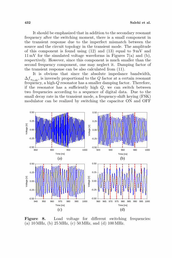
, is inversely proportional to the Q factor at a certain resonantfrequency, a high-Q resonator has a smaller damping factor. Therefore,if the resonator has a sufficiently high Q, we can switch betweentwo frequencies according to a sequence of digital data. Due to thesmall decay rate in the transient mode, a frequency-shift keying (FSK)modulator can be realized by switching the capacitor ON and OFF
(a)
(c) (d)
Time [ns]
850 900 950 1000
Vol
tage
[V]
-0.50
-0.25
0.00
0.25
0.50
920 940 960 980 1000
Time [ns]
940 950 960 970 980 990 1000
Time [ns]
960 965 970 975 980 985 990 995 1000
(b)Time [ns]
Vol
tage
[V]
-0.50
-0.25
0.00
0.25
0.50
Vol
tage
[V]
-0.50
-0.25
0.00
0.25
0.50
Vol
tage
[V]
-0.50
-0.25
0.00
0.25
0.50
Figure 8. Load voltage for different switching frequencies:(a) 10 MHz, (b) 25MHz, (c) 50 MHz, and (d) 100 MHz.

Progress In Electromagnetics Research, Vol. 143, 2013 433
based on a data-coded controlling signal.In order to preserve the stored energy, both switch-ON and switch-
OFF instants should be synchronous with the zero-crossing of thecapacitor voltage. In other words, the switching frequency mustbe a common factor of two resonant frequencies. Figure 8 showsthe load voltage for different switching frequencies, 10, 25, 50 and100MHz. Duty cycle of the modulating pulse is 50% and each pulserepresents a pair of 0 and 1 with bit duration of Tb, where 2Tb is thepulse period. In order to generate orthogonal FSK signals, separationbetween frequencies should be an integer multiplication of switchingfrequency fs = 1/Ts [29]. Since each switching pulse represents a pairof 0 and 1, bit-rate is twice the switching frequency. In fact, by using afast switching mechanism, a simple narrowband RLC resonator excitedby a single-tone source can be employed to generate a high data-rateFSK signal. 1st frequency is the same as the source frequency and 2ndfrequency can be tuned by the switched capacitor.
4. DIRECT FSK MODULATION USING A NARROW-BAND SWITCHED-ANTENNA
As discussed in Section 2, a single-mode small antenna can be modeledby an RLC resonator that mimics the antenna in both time andfrequency domain. As a result, the switched-capacitor techniquepresented in Section 3 can be applied to a small antenna in orderto realize a high bit-rate direct FSK modulation. A great benefitof employing the switched-capacitor technique to create a directantenna modulation is that the data-rate is not limited by the antennabandwidth. Figure 9 shows the block diagram of the direct BFSKmodulation. Two capacitors, C1 and C2 are used to tune the antennaat f1 and f2, respectively. The antenna is fed at f1 and a single pole-double throw (SPDT) switch controlled by the data sequence is usedto switch between the resonant frequencies.
Starting at t = 0, C1 loads the antenna and reactive energy beginsto build up at frequency f1. A portion of the energy is stored in C1
and the rest is stored in the near-field zone of the antenna. At themoment of zero-crossing of the capacitor voltage, the switch changesits state to connect C2 and shifts the fundamental natural resonanceof the antenna to f2. Hence, the antenna will operate in the transientmode and radiating fields shift to f2. Since the capacitor C1 doesn’tface a voltage discontinuity, the stored electric energy is not disturbedand if the capacitor is high-Q, the entire stored energy is preserveduntil the next cycle of charging.
Depending on the time constant, after several cycles, stored energy

434 Salehi et al.
in the near-field and capacitors builds up to a maximum. During thetransient operation of the antenna, the stored energy within the near-field decays slightly and provides the radiative power. The amountof energy decay depends on the Q factor of the antenna. Therefore,if the antenna has a high Q, total amount of near-field stored energywill not change dramatically and the bandwidth of the antenna willbe decoupled from the stored energy, i.e., any abrupt variation in thesurface current distribution will appear in the far-field momentarily, ifthe transmission delay is ignored.
By using a pulse train as the switch control signal where a pair of“0” and “1” can be represented by each pulse cycle, f1 associated withC1 represents a “1” and C2 associated with f2 represents a “0”.
In contrast with the resonator, an antenna may excite higherorder modes. Even though the higher order modes have largerdamping factors, part of the input power may couple to thesemodes and high-order resonances appear in the radiated fields. Asmall antenna typically excites the fundamental mode; however, forswitching application an antenna structure with only one excitednatural resonance is required. Recently, an electrically-coupled loopantenna (ECLA) has been introduced as a dual for planar inverted-F antenna (PIFA) [30]. Since ECLA uses an electrically coupledfeeding mechanism, further impedance matching is not required andthe antenna can be highly miniaturized. As a result, the antenna canoperate at a single resonance with a very high Q factor. In addition,ECLA shows excellent radiation efficiency compared to its counterpart,PIFA. These considerations make the ECLA a suitable choice for theproposed modulation technique.
Figure 10 shows the structure of ECLA. The antenna is fed viaa capacitive plane (Wf ) which is used to match the input impedance.
Source(f )1
High-Q antennaRadiation(f & f )1 2
DataSequence SPDT Switch
C1 C2
Figure 9. Block diagram of the proposed direct BFSK modulation.

Progress In Electromagnetics Research, Vol. 143, 2013 435
(a)
(b)
W f
L
L
Wc
hc
fh
W
W f
Tuningport
Figure 10. Structure of the electrically-coupled loop antenna(ECLA): (a) perspective view and (b) side view.
Frequency [MHz]
300 400 500 600 700
S11
[dB
]
-20
-15
-10
-5
0
UnloadedC1=1.93 pFC2=4.74 pF
Figure 11. Return loss of a simulated ECLA with L = 20 mm, W =15mm, wf = 3.2mm, hc = 0.5mm, wc = 10 mm and hf = 2.5mm.
The loop (L × L ×W ) resonates along with a tunable capacitive gap(hc) that tunes the resonant frequency and miniaturizes the antenna.In order to change the resonant frequency, the tuning port is locatedat the edge of the capacitive gap. Therefore, a switched capacitor canbe placed in parallel with the capacitive gap and contribute to thenatural resonance of the antenna. Figure 11 shows the return loss ofa simulated ECLA with L = 20 mm, W = 15 mm, wf = 3.2mm,hc = 0.5mm, wc = 10 mm and hf = 2.5mm. The unloadedantenna resonates at f0 = 630 MHz with 1.65 MHz 3-dB bandwidth(Q0 ≈ 382). The electrical dimension of the unloaded antenna is0.04λ × 0.04λ × 0.03λ. By loading the antenna with two capacitors

436 Salehi et al.
C1 = 1.93 pF and C2 = 4.74 pF, resonant frequency can be tunedat f1 = 500 MHz and f2 = 400 MHz with a 3-dB bandwidth ofB1 = 1.6MHz and B2 = 0.8MHz (Q1 = 312.5 and Q2 = 500).
Figure 12 shows the simulation set-up for the switched antenna.A small dipole is placed 1 meter away from the antenna in the E-planeto measure the electric field. The measuring dipole is aligned with theco-pol direction and terminated by a high impedance. As discussedin Section 3, in order to preserve the stored energy in the capacitors,switching moment must be synchronous with the zero-crossing of thecapacitors voltage. This requires the resonant frequencies to be integermultiples of the switching frequency.
Source (500 MHz)
VRInput port
C =4.74 pF2
Tuning port
1 m +
-
Vc1
Vc2
C =1.93 pF1SPDT Switch
Figure 12. Simulation set-up for the switched antenna.
It is worthwhile to point out that due to the transmission-line delay, voltage zero-crossings may slightly change. This can becompensated by delaying the switch signal such that the switchingmoments coincide with the voltage zero-crossing of the capacitors.Figure 13 shows the voltage of the capacitors in conjunction withswitching signal at 50 MHz. Since the distance between the feeding andtuning ports is small, transmission-line delay would not be significantwith this configuration.
The switching signal is a two-level voltage waveform. “0” indicatesthe OFF state of the switch which is associated with the capacitor C1
and frequency f1, while “1” indicates the ON state of the switch whichputs the capacitor C2 in charge of the transient radiation at frequencyf1.
Figure 14 shows the received signal by the measuring dipole for4 different switching frequencies: 10, 25, 50 and 100MHz. Since eachpulse represents two bits, the bit-rate is twice the switching frequency.

Progress In Electromagnetics Research, Vol. 143, 2013 437
.
Time [µs]0.95 0.96 0.97 0.98 0.99 1.00
Cap
acito
r V
olta
ge [V
]
-0.6
-0.3
0.0
0.3
0.6
VC1
VC2
Time [µs]0.95 0.96 0.97 0.98 0.99 1.00
Sw
itch
sign
al [V
]
0.00
0.25
0.50
0.75
1.00
Figure 13. Voltage of the capacitors in conjunction with switchingsignal at 50MHz.
It can be seen that regardless of the extremely narrow bandwidth ofthe antenna, bit-rate can be as high as the carrier frequency. Thishigh bit-rate achievement is mainly due to two factors. Firstly, thetime-varying property of the antenna obviates the need for coveringthe carrier frequency deviation, ∆f = f2 − f1. In other words, theantenna is instantaneously tuned to f1 and f2 when logic “0” and“1” are to be transmitted, respectively. Secondly, since the loadingcapacitors change the natural resonances of the antenna, near-fieldreactive energy switches between different frequencies. After severalswitching cycles, the stored energy reaches a maximum and afterwards,the fields shift between two resonant frequencies due to variation of theantenna’s fundamental resonance, resulting in radiative power shiftsbetween the two frequencies. The nature of this frequency shiftingarises from the variation of antenna poles and is not linked to theantenna input signal. Therefore, if the antenna is sufficiently high-Qand the switching moment is properly chosen such that during thetransient mode the stored energy doesn’t discharge dramatically and

438 Salehi et al.
1.30 1.35 1.40 1.45 1.50
Vol
tage
[mV
]
-0.6
-0.3
0.0
0.3
0.6
1.46 1.47 1.48 1.49 1.50 1.460 1.465 1.470 1.475 1.480 1.485 1.490 1.495 1.500
Time [µs] Time [µs]
1.30 1.35 1.40 1.45 1.50
Vol
tage
[mV
]
-0.6
-0.3
0.0
0.3
0.6
Vol
tage
[mV
]
-0.6
-0.3
0.0
0.3
0.6
Vol
tage
[mV
]
-0.6
-0.3
0.0
0.3
0.6
(a)
(c) (d)
(b)
Time [µs] Time [µs]
Figure 14. Simulated received signals by the measuring dipoleat switching frequencies: (a) 10 MHz, (b) 25MHz, (c) 50MHz and(d) 100 MHz.
remains close to its maximum, the conventional impedance bandwidthwill not limit the radiation bandwidth and the antenna is able torespond to any fast frequency shifting caused by switching the naturalresonances.
5. EXPERIMENTAL RESULTS
To validate the proposed technique, an ECLA was prototyped andmeasured. The experiments are performed at a low frequency inorder to implement a high-Q antenna and achieve a good isolationbetween the two alternating frequencies. In addition, realizing anultra-fast and high-Q switching mechanism is a challenge as most ofthe commercial RF switches suffer from a relatively high insertion lossand low speed. Nevertheless, ultra-fast switching can be addressedby recently developed technologies such as SiGe transistors [31]. The

Progress In Electromagnetics Research, Vol. 143, 2013 439
(a) (b)
Figure 15. (a) Prototyped antenna with dimensions: L = 100 mm,W = 30mm, wf = 25 mm, hc = 0.51mm, wc = 30 mm andhf = 2.5mm, (b) switching circuitry attached to the antenna on aRT/Duroid 5880 with thickness 20 mil.
Switchsignal
LPF
C1pf
L1pfC t
PIN diode
Antenna
RFsource
Figure 16. Switching circuitry.
prototyped antenna is shown in Figure 15 with dimensions: L =100mm, W = 30mm, wf = 25 mm, hc = 0.51 mm, wc = 30 mmand hf = 2.5 mm. The bottom side of the antenna that includes theswitch circuitry is supported by a 20 mil Rogers RT/duroid 5880. Inour experiment, we use a low-loss PIN diode (Avago HSMP-482) in ashunt arrangement as depicted in Figure 16 which shows the switchingcircuitry. The switching signal is separated from the antenna by alow pass filter. When the PIN diode is in reverse bias (switch-OFF),tuning port is open-circuited and the antenna is not loaded. Thereforethe antenna resonates at its original resonant frequency, f1. In theforward-bias state (switch-ON), the antenna is loaded by the capacitorCt through a 0.6 Ω resistance of the forward-biased PIN diode andresonates at the lower frequency, f2.
Although the capacitors and PIN diode are chip components,however due to relatively low-Q properties, particularly for thecapacitors, measurement shows that the loaded Q is considerablyaffected. Figure 17 compares the measured return loss with the results

440 Salehi et al.
Frequency [MHz]
30 40 50 60 70
S
[dB
]11
Switch-ON (Meas)Switch-OFF (Meas)Switch-ON (Sim)Switch-OFF (Sim)
-25
-20
-15
-10
-5
0
Figure 17. Measured and simulated return loss.
Time [ns]
0 200 400 600 800 1000
Ano
de v
olta
ge [V
]
-4
-3
-2
-1
0
1
OFF to ONON to OFF
Time [ns]
0 500 1000 1500 2000
Ano
de v
olta
ge [V
]
-4
-3
-2
-1
0
1
(a) (b)
Figure 18. Measured voltage waveform across the PIN diode:(a) comparing the ON and OFF times and (b) switch signal is a 2MHzperiodic pulse varying between ±2 V with 50% duty-cycle.
of full-wave simulation that uses an ideal capacitor. The measuredresonant frequencies are f1 = 57.75 MHz and f2 = 42 MHz where thetuning capacitor is Ct = 47 pF. The low pass filter with Clpf = 470 pFand Llpf =1µH provides a suppression equal to 30 dB and 25 dB atfrequencies f1 and f2, respectively. Measured Q factors at f1 andf2 are Q1 = 18.6 and Q2 = 52.5. The magnitude of return loss ateach frequency is measured less than 0.04 dB when the antenna istuned to the other frequency and hence the leakage is sufficiently small.Since the Q factors are still much greater than one and two resonantfrequencies are well-isolated from each other, this configuration canbe used to validate the proposed technique. The maximum practical

Progress In Electromagnetics Research, Vol. 143, 2013 441
bit-rate in our experiment depends on the switching speed which isdetermined by the PIN diode rise and fall time. Figure 18(a) showsthe measured response of the utilized PIN diode to a step-like functionvarying between ±2V. The ON and OFF time based on 0 to 0.65Vand vice versa is measured about 65 ns. This limits the switching speedto about 15MHz. Also, the PIN diode exhibits an overshoot about 1.5times the biasing voltage at the falling edge causing the OFF timeto be shortened. The switch signal measured as the anode voltage atfrequency 2 MHz is shown in Figure 18(b). Even though the duty cycleof the pulse is 50%, the switch-ON duration associated with the lowerfrequency, f2, is approximately twice the switch-OFF duration thatrepresents the higher frequency, f1.
Figure 19 shows the voltage waveform at the receiving dipole whenthe switched ECLA is in transmitting mode. The RF source is an R&S
1.0 1.2 1.4 1.6 1.8 2.0
Rec
eive
d vo
ltage
[mV
]
-2
-1
0
1
2
Rec
eive
d vo
ltage
[mV
]
-2
-1
0
1
2
1.5 1.6 1.7 1.8 1.9 2.0
Rec
eive
d vo
ltage
[mV
]
-2
-1
0
1
2
1.5 1.6 1.7 1.8 1.9 2.0
Rec
eive
d vo
ltage
[mV
]
-2
-1
0
1
2
Time [µs] Time [µs]
(a)
(c) (d)
(b)
Time [µs] Time [µs]
1.0 1.2 1.4 1.6 1.8 2.0
Figure 19. Measured voltage waveform received by a small dipolefor different switching frequencies: (a) fs = 2 MHz, (b) fs = 4 MHz,(c) fs = 8 MHz, and (d) fs = 12 MHz.

442 Salehi et al.
ZVA50 vector network analyzer in the CW mode which excites theantenna at the frequency f2 = 42MHz. A Tektronix AFG3252 signalgenerator is used to provide a periodic pulse as the switching signal.Time-domain electric fields are measured by a Tektronix MSO4102oscilloscope with 1 MΩ input impedance. The electric fields shown inFigure 19 are measured at switching frequencies 2 MHz, 4MHz, 8 MHzand 12 MHz. It can be seen that even though the antenna bandwidthis measured about 3 MHz at the upper band, an FSK modulation witha bit-rate equal to R = 2×12 = 24 Mb/s is realized. The restriction onthe switching frequency is due to the time constant of the low-pass filterand also the ON and OFF time of the PIN diode. Hence, the bit-ratecan be further improved by using a faster switch and improving thefilter performance. For demonstration purposes, the antenna has alsobeen measured in the receiving mode. Figure 20 shows the receivedvoltage at the input port of the ECLA when connected to a 1 MΩoscilloscope. Both frequencies are on the air with the same powerlevel. Similar to the transmitting mode, the switched antenna receivesboth frequencies according to the switching frequency.
1.0 1.2 1.4 1.6 1.8 2.0Rec
eive
d vo
ltage
[mV
]
1.0 1.2 1.4 1.6 1.8 2.0Rec
eive
d vo
ltage
[mV
]
-100
-50
0
50
100
Time [µs] Time [µs]
(a) (b)
-100
-50
0
50
100
Figure 20. Measured voltage waveform received by the ECLA whenoperating in Rx mode at different switching frequencies: (a) fs =5MHz and (b) fs = 10 MHz.
6. CONCLUSION
A new technique to realize a wideband data-transmission by usinga narrowband antenna was presented. The proposed technique usesthe transient property of a high-Q antenna to implement a binaryFSK modulation with a high data-rate. The properties of a switchedresonator was studied and it was shown that if the Q factor issufficiently high such that the transient damping factor is small, theresonator or antenna can be switched to the transient mode andgenerate a binary FSK signal by using only a single source with aproper switching frequency. An electrically coupled loop antenna wasprototyped and measured to validate the proposed technique.

Progress In Electromagnetics Research, Vol. 143, 2013 443
ACKNOWLEDGMENT
This work is supported in part by Intel Corp.. The authors thankShyam C. Nambiar for his help in preparing this manuscript.
REFERENCES
1. Ghovanloo, M. and K. Najafi, “A wideband frequency-shift keyingwireless link for inductively powered biomedical implants,” IEEETransactions on Circuits and Systems I: Regular Papers, Vol. 51,No. 12, 2374–2383, Dec. 2004.
2. Miranda, H., V. Gilja, C. A. Chestek, K. V. Shenoy, andT. H. Meng, “HermesD: A high-rate long-range wireless transmis-sion system for simultaneous multichannel neural recording appli-cations,” IEEE Transactions on Biomedical Circuits and Systems,Vol. 4, No. 3, 181–191, Jun. 2010.
3. Lee, S. B., M. Yin, J. R. Manns, and M. Ghovanloo, “A widebanddual-antenna receiver for wireless recording from animals behavingin large arenas,” IEEE Transactions on Biomedical Circuits andSystems, Vol. 60, No. 7, 1993–2004, Jul. 2013.
4. Chu, L. J., “Physical limitations on omni-directional antennas,”Journal of Applied Physics, Vol. 19, 1163–1175, Dec. 1948.
5. Harrington, R. F., “Effect of antenna size on gain, bandwidth,and efficiency,” Journal of Research of the National Bureau ofStandards, Vol. 64D, 1–12, Jan.–Feb. 1960.
6. McLean, J. S., “A re-examination of the fundamental limits on theradiation Q of electrically small antennas,” IEEE Transactions onAntennas and Propagation, Vol. 44, No. 5, 672–675, May 1996.
7. Salehi, M. and M. Manteghi, “Utilizing non-linear inductors forbandwidth improvement,” URSI-USNC National Radio ScienceMeeting, Boulder, CO, 2011.
8. Salehi, M. and M. Manteghi, “Bandwidth enhancement usingnonlinear inductors,” 2011 IEEE Antennas and PropagationSociety International Symposium (APSURSI), 1–4, 2011.
9. Manteghi, M., “An inexpensive phased array design usingimpedance modulation,” URSI-USNC National Radio ScienceMeeting, Boulder, CO, 2010.
10. Manteghi, M., “Non-LTI systems, a new frontier in electromag-netics theory,” 2010 IEEE Antennas and Propagation Society In-ternational Symposium (APSURSI), 1–4, 2010.

444 Salehi et al.
11. Manteghi, M., “Antenna miniaturization beyond the fundamentallimits,” URSI-USNC National Radio Science Meeting, Boulder,CO, 2009.
12. Manteghi, M., “A switch-band antenna for software-defined radioapplications,” IEEE Antennas and Wireless Propagation Letters,Vol. 8, 3–5, 2009.
13. Manteghi, M., “Antenna miniaturization beyond the fundamentallimits using impedance modulation,” 2009 IEEE Antennas andPropagation Society International Symposium, (APSURSI), 1–4,2009.
14. Wheeler, H. A., “Fundamental limitations of small antennas,”Proceedings of the IRE, Vol. 35, No. 12, 1479–1484, Dec. 1947.
15. Schaubert, D. H., “Application of Prony’s method to time-domain reflecto-meter data and equivalent circuit synthesis,”IEEE Transactions on Antennas and Propagation, Vol. 27, No. 2,180–184, Mar. 1979.
16. Schelkunoff, S. A., “Representation of impedance functions interms of resonant frequencies,” Proceedings of the IRE, Vol. 32,No. 2, 83–90, Feb. 1944.
17. Kim, Y. and H. Ling, “Equivalent circuit modeling of broadbandantennas using a rational function approximation,” Microwaveand Optical Technology Letter, Vol. 48, No. 5, 950–953, May 2006.
18. Adve, R. S., T. K. Sarkar, S. M. Rao, E. K. Miller, andD. R. Pflug, “Application of the cauchy method for extrapolat-ing/interpolating narrow-band system responses,” IEEE Transac-tions on Microwave Theory and Techniques, Vol. 45, No. 5, 837–845, May 1997.
19. Michalski, K. A. and L. W. Pearson, “Equivalent circuit synthesisfor a loop antenna based on the singularity expansion method,”IEEE Transactions on Antennas and Propagation, Vol. 32, No. 5,433–441, May 1984.
20. Simpson, T. L., J. C. Logan, and J. W. Rockway, “Equivalentcircuits for electrically small antennas using LS-decompositionwith the method of moments,” IEEE Transactions on Antennasand Propagation, Vol. 37, No. 12, 1632–1635, Dec. 1989.
21. Hamid, M. and R. Hamid, “Equivalent circuit of dipole antennaof arbitrary length,” IEEE Transactions on Antennas andPropagation, Vol. 45, No. 11, 1695–1696, Nov. 1997.
22. Love, A. W., “Equivalent circuit for aperture antennas,”Electronics Letters, Vol. 23, No. 13, 708–710, 1987.
Progress In Electromagnetics Research, Vol. 143, 2013 445
23. Vainikainen, P., J. Ollikainen, O. Kivekas, and I. Kelander,“Resonator-based analysis of the combination of mobile handsetantenna and chassis,” IEEE Transactions on Antennas andPropagation, Vol. 50, No. 10, 1433–1444, Oct. 2002.
24. Tang, T. G., Q. M. Tieng, and M. W. Gunn, “Equivalent circuit ofa dipole antenna using frequency-independent lumped elements,”IEEE Transactions on Antennas and Propagation, Vol. 41, No. 1,100–103, Jan. 1993.
25. Streable, G. W. and L. W. Pearson, “A numerical study onrealizable broad-band and equivalent admittances for dipoleand loop antennas,” IEEE Transactions on Antennas andPropagation, Vol. 29, No. 5, 707–717, Sep. 1981.
26. Liu, G. K. H. and R. D. Murch, “Compact dual-frequency PIFAdesign using LC resonators,” IEEE Transactions on Antennas andPropagation, Vol. 49, No. 7, 1016–1019, Oct. 2001.
27. Chu, L. J., “Physical limitations of omni-directional antennas,”Journal of Applied Physics, Vol. 19, 1163–1175, Dec. 1948.
28. Davis, W. A., T. Yang, E. D. Caswell, and W. L. Stutzman,“Fundamental limits on antenna size: A new limit,” IETMicrowaves, Antennas & Propagation, Vol. 5, No. 11, 1297–1302,2011.
29. Proakis, J. G. and M. Salehi, Digital Communications, 5thEdition, McGraw Hill, NY, 2008.
30. Manteghi, M., “Electrically coupled loop antenna as a dual for theplanar inverted-F antenna,” Microwave and Optical TechnologyLetters, Vol. 55, No. 6, 1409–1412, Jun. 2013.
31. Hancock, T. M. and G. M. Rebeiz, “Design and analysis of a 70-ps SiGe differential RF switch,” IEEE Transactions on MicrowaveTheory and Techniques, Vol. 53, No. 7, 2403–2410, Jul. 2005.