A VLSl Single (255,223) Reed-Solomon Encoder With lnterleaver
7
TDA Progress Report 42-89 January-March 1987 A VLSl Single Chip (255,223) Reed-Solomon Encoder With lnterleaver I. S. Hsu, L. J. Deutsch, and T. K. Truong Communications Systems Research Section I. S. Reed Electrical Engineering Department University of Southern California This article presents a description of a single-chip implementation of a Reed-Solomon encoder with interleaving capability. The code used was adapted by the CCSDS (Consula- tive Committee on Space Data Systems). It forms the outer code of the NASA standard concatenated coding system which includes a convolutional inner code of rate 112 and constraint length 7. The architecture, leading to this single VLSI chip design, makes use of a bit-serial finite field multiplication algorithm due to E. R . Berlekamp. 1. Introduction A concatenated coding system consisting of a convolutional inner code and a Reed-Solomon outer code has been adopted as a guideline for downlink telemetry for future space missions by CCSDS (Consultative Committee for Space Data Systems) [I]. The participants in t h s committee include the European Space Agency (ESA) and NASA as well as space agencies from many other nations. The convolutional inner code is the same (7,1/2) code used by NASA’s Voyager project. The outer Reed-Solomon code is a (255, 223) block code on 8-bit symbols and it is capable of correcting up to 16 symbol errors. The performance of such a scheme is investigated in [2]. It is shown that this concate- nated channel provides a coding gain of almost 2 dB over the convolutional-only channel at a decoded bit error rate of One of the benefits of concatenated coding, and one of the main motivations for its acceptance as a standard system, is that it provides for nearly error free communication links at fairly low signal power levels. This means that source data compression techniques [3] can be used to help increase channel throughput without a substantial change in overall error rate. Data compression algorithms, while promising to remove substantial information redundancy are very sensitive to transmission errors. An end-to-end study of a system using concatenated coding with data compression can be found in [41. The interleaving buffers are required because the inner decoder errors tend to occur in bursts, which occasionally are as long as several constraint lengths. The outer decoder remains undisturbed by burst errors which occur within a given 8-bit symbol (which corresponds to about one con- 41
Transcript of A VLSl Single (255,223) Reed-Solomon Encoder With lnterleaver
TDA Progress Report 42-89 January-March 1987
A VLSl Single Chip (255,223) Reed-Solomon Encoder With lnterleaver
I. S. Hsu, L. J. Deutsch, and T. K. Truong Communications Systems Research Section
I. S. Reed Electrical Engineering Department University of Southern California
This article presents a description of a single-chip implementation o f a Reed-Solomon encoder with interleaving capability. The code used was adapted by the CCSDS (Consula- tive Committee on Space Data Systems). It forms the outer code of the NASA standard concatenated coding system which includes a convolutional inner code of rate 112 and constraint length 7. The architecture, leading to this single VLSI chip design, makes use of a bit-serial finite field multiplication algorithm due to E. R . Berlekamp.
1. Introduction A concatenated coding system consisting of a convolutional
inner code and a Reed-Solomon outer code has been adopted as a guideline for downlink telemetry for future space missions by CCSDS (Consultative Committee for Space Data Systems) [ I ] . The participants in t h s committee include the European Space Agency (ESA) and NASA as well as space agencies from many other nations.
The convolutional inner code is the same (7,1/2) code used by NASA’s Voyager project. The outer Reed-Solomon code is a (255, 223) block code on 8-bit symbols and it is capable of correcting up to 16 symbol errors. The performance of such a scheme is investigated in [2]. It is shown that this concate- nated channel provides a coding gain of almost 2 dB over the convolutional-only channel at a decoded bit error rate of
One of the benefits of concatenated coding, and one of the main motivations for its acceptance as a standard system, is that it provides for nearly error free communication links at fairly low signal power levels. This means that source data compression techniques [3] can be used to help increase channel throughput without a substantial change in overall error rate. Data compression algorithms, while promising to remove substantial information redundancy are very sensitive to transmission errors. An end-to-end study of a system using concatenated coding with data compression can be found in [41.
The interleaving buffers are required because the inner decoder errors tend to occur in bursts, which occasionally are as long as several constraint lengths. The outer decoder remains undisturbed by burst errors which occur within a given 8-bit symbol (which corresponds to about one con-
41
straint length of the inner convolutional code). However, its performance is severely degraded by highly correlated errors among several successive symbols. As a consequence, inter- leaving is required for best performance.
A Reed-Solomon encoder is basically a circuit which performs polynomial division in a finite field. Such circuits are well known [5] and the implementation is straight for- ward. The major problem in designing a small encoder is the large quantity of hardware that is necessary to perform the finite field multiplications.
Due to the limited weight, space and power that can be allotted to a spacecraft instrument, the equipment used must be as light and as small as possible. Therefore, a single chip Reed-Solomon encoder can have a significant advantage in deep-space probe missions. Such an encoder represents a considerable space, weight and power savings over the smallest existing encoder (about 30 chips).
A conventional encoder described in [SI for the (255,223) RS code, requires 32 finite field multipliers. These multipliers are usually implemented as full parallel multipliers or table lookup multipliers. The use of either of these multiplication algorithms prohibits the implementation of the encoder on a single medium density VLSI chip.
Fortunately, E, R. Berlekamp [ 6 ] developed a serial algo- rithm for finite field multiplication over a binary field. Berle- kamp’s algorithm requires only shifting and exclusive-OR operation. Recently, it is shown [7] that this multiplication algorithm makes possible the design of a workable VLSI architecture and that this new dual-basis (255, 223) RS encoder can be readily realized on a single VLSI chip with NMOS technology.
In this article, an extension of the previous work is pre- sented. It is demonstrated in this article that a (255, 223) RS encoder with 5-depth interleaving capability also can be implemented on a single VLSI chip with NMOS technology.
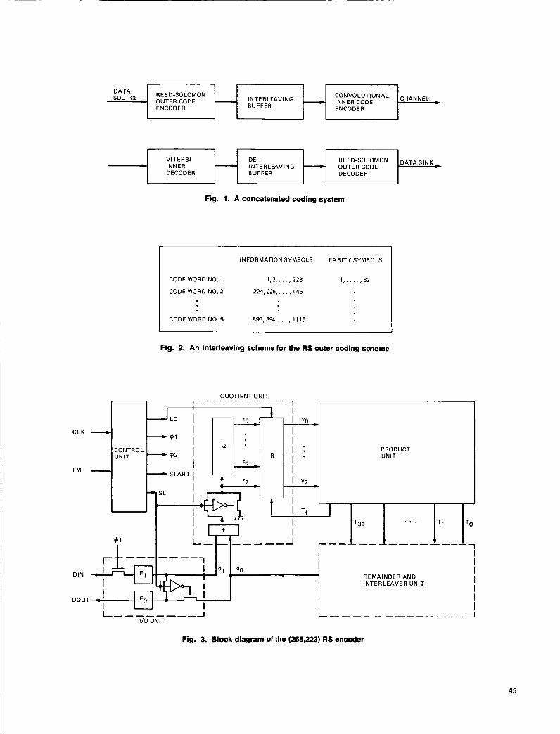
II. Review of Interleaving Algorithm The basic block diagram of a concatenated coding system
is shown in Fig. 1. The inner encoder-decoder is a convolu- tional encoder, while the receiver utilizes Viterbi (maximum likelihood) decoder. The outer code is a high rate block code.
It is demonstrated [ 2 ] that this concatenated channel provides more than 2 dB of coding gain over the convolutional- only channel. However, the performance of the recommended Reed-Solomon coding scheme in the concatenated coding
system can only be achieved when the bursts of errors appear- ing at the Viterbi decoder output are dispersed in such a manner that the RS symbols at the outer decoder input are randomized sufficiently. This randomization can be achieved by interleaving [ 151 .
In the (255, 223) RS code, each code word contains 255 symbols, and each symbol contains 8 bits. These symbols are grouped into frames. The frames, together, form a block or format. Figure 2 shows an interleaving scheme for the RS outer coding scheme. The numbers used in this figure are for illustration purposes only.
To achieve interleaving, the information and parity symbols are transmitted column-by-column from left-to-right and each column from top-to-bottom. As a result, a bursty error event of the Viterbi decoder will tend to affect only one symbol of each code word provided the number of rows in each inter- leaving array is sufficiently high. This number is called the interleaving depth.
The standard RS interleaving depths used for deep-space probes are less than or equal to five [ l ] . As a consequence, a chip was designed which is capable of being programmed. The interleaving depth can be changed from one to five at the user’s convenience.
111. A Single VLSI Chip of a (255,223) RS Encoder With lnterleaver
Berlekamp’s bit-serial multiplication algorithm for a (255, 223) RS-encoder over GF (2*) is presented in [7] and [8] (also see M. Perlman and J. J . Lee “Reed-Solomon Encoders- Conventional Versus Berlekamp’s Architecture,” JPL Internal Document, No. 3610-81-1 19ISMP, dated July, 1981). The block diagram of the (255, 223) RS encoder with program- mable interleaver is exhibited here in Fig. 3.
In Fig. 3, one observes that the circuit is divided into five units: the Product unit, Remainder and Interleaver unit, Quotient unit, I/O unit, and Control Unit. The use of each unit is explained in detail in [8]. However, the Remainder and Interleaver unit is different from that in [8 ] . This is due to the fact that the interleaver is included in this design, while in [8] , no such capability was available.
The function of the Remainder and Interleaver unit is dis- cussed in detail in what follows. Figure 4 shows the block diagram of the Remainder and Interleaver unit. The Remainder and Interleaver unit is used to store the coefficients of the remainder during the division process. This unit also performs the interleaving operation.
42

In Fig. 4, Si .’s for 0 Q i Q 30, 1 Q j Q 5 are 8-bit shift registers. The addition used in the circuit is a modulo 2 addi- tion or Exclusive-OR operation.
The “Turn” and “No-turn” signals are used to program the interleaving depth and the “No-turn’’ signals are the logical complement of the corresponding “Turn” signals. For example, if “Turn 2” equals 1 and all other “Turn” signals equal 0, then obviously signal “No-turn 2” will equal 0 and all other “No-turn” signals will equal 1. These will turn transistors T2, T3, T6, T8, T9 and transistors in the corresponding positions in Fig. 2 on. Also, transistors Tl, T4, T5, T,, T l0 , Tl l , Tlz and their corresponding transistors in Fig. 2 will be turned off. Therefore, data can be transferred from registers Si, l’s to Si,2’s for 0 d i d 30.
The outputs of registers Si,2’s, for 0 Q i d 30, are sent to the inputs of modulo 2 adders by bus lines Lis , for 1 Q i Q 3 1. Since transistor T4 and transistors in its corresponding posi- tions in Fig. 4 are off, outputs of Si,2’s can not be sent to Si,3’s, for 0 < i < 30, which means only a depth of 2 inter- leaving operation is allowed in this manner. The depths of 3, 4 or 5 of interleaving can be carried out similarly.
An overall block diagram of the chip is shown in Fig. 5. In Fig. 5 , V,, and GND are power pins. The signals and qj2 are the two phases of a system clock. The information symbols are fed into the chip serially through the data-in pin, DIN.
Similarly, the encoded code word is transmitted out of the chip sequentially from the data-out pin, DOUT.
The control signal, SL, is set to 1 (logic 1) when the inform- ation symbols are loaded into the chip. After this, SL is set to 0. The control signal “START” resets a 3-bit word counter in the chip before the encoding process begins. The “Turn” signals are used to program the interleaving depth.
The entire chip was simulated on a general purpose com- puter using ESIM (a logic level simulation program) [9] and SPICE (a transistor level circuit simulation program) [ 101 . The layout of this chip was accomplished using the program CAESAR [12]. LYRA [12] was used to check the resulting layout against a set of geometric rules supplied by the fabri- cator. Timing simulation was accomplished using CRYSTAL ~ 4 1 .
This circuit comprises about 10,000 transistors. It was fabricated using the MOSIS service [13] . The technology used is 4 p m NMOS. The layout of this encoder is shown in Fig. 6 . The chip was successfully tested and the maximum clock frequency is about 1.5 MHz. The operating speed of this chip is limited mainly by the long clock lines associate with the two-phase clocks used in the dynamic shift registers and there are more than 1250 dynamic registers used on this chip. The chip area is about 4800 X 3220 pm2. The power consumption at the maximum clock frequency is about 300 mW.
43

References
[ 11 “Recommendation for Space Data System Standards: Telemetry Channel Coding,“ (Blue Book), Consulative Committee for Space Data Systems, CCSDS Secretariat, Communications and Data Systems Division, Code TS, NASA, Washington, D.C., May 1984.
[2] R. L. Miller, L. J. Deutsch and S . A. Butman, “On the Error Statistics of Viterbi Decoding and the Performance of Concatenated Codes,” JPL Publication, 81-9, Jet Propulsion Laboratory, Pasadena, California, pp. 33-39, September 1, 1981.
[3] R. F. Rice, “Some Practical Universal Noiseless Coding Techniques,” JPL Publica- tion, 79-22, Jet Propulsion Laboratory, Pasadena, California, March 15, 1979.
[4] R. F. Rice, “End-To-End Imaging Information Rate Advantages of Various Alter- native Communication Systems,” JPL Publication, 82-61, Jet Propulsion Lab- oratory, Pasadena, California, September 1, 1982.
[5] W. W. Peterson and E. J. Weldon Error-Correcting Codes, Cambridge: MIT Press, 1972.
[6] E. R. Berlekamp, “Bit-Serial Reed-Solomon Encoders,” IEEE Trans. on Informa-
[7] I. S. Hsu, L. J. Deutsch, T. K. Truong, and I. S. Reed, “A VLSI Single Chip (255 , 223) Reed-Solomon Encoder,” TDA Progress Report 42-83, vol. July-September 1985, Jet Propulsion Laboratory, Pasadena, California, pp. 51-56, November 15, 1985.
[8] I. S. ”I, I. S . Reed, T. K. Truong, K. Wang, C. S. Yeh, and L. J. Deutsch, “The VLSI Implementation of a Reed-Solomon Encoder Using Berlekamp’s Bit-Serial Multiplier Algorithm,” IEEE Trans. on Computers, Vol. C-33, No. 10, pp. 906- 91 1 , October 1984.
[9] C. Terman, “ESIM - An Event Driven Simulator,” Documentation of 1983 VLSI Tools, Computer Science Division, Univerisity of California, Berkeley, California, 1983.
[ lo ] L. W. Negal and D. 0. Pederson, “SPICE - Simulation Program with Integrated Circuit Emphasis,” Memorandum No. ERL-4382, Electronic Research Laboratory, University of California, Berkeley, April, 1973.
[ 111 J. Ousterhout, “CAESAR - Editing VLSI Circuit with CAESAR,” Documentation o f 1 983 VLSI Tools, Computer Science Division, University of California, Berkeley, California, 1983.
[12] J. Ousterhout, “LYRA - A Design Rule Checker,” Documentation of 1983 VLSI Tools, Computer Science Division, University of California, Berkeley, California, 1983.
[13] MOSIS Project, “The MOSIS System (what it is and how to use it),” Information Science Institute, University of Southern California, Publication ISI/TM-84-128, Marina Del Rey, California, 1984.
[14] J. Ousterhout, “Using Crystal for Timing Analysis,” Documentation of I983 VLSI Tools, Computer Science Division, University of California, Berkeley, California, 1983.
[ 151 J. L. Ramsey, “Realization of Optimum Interleavers,” IEEE Trans. on Information
tion Theory, vol. IT-28, No. 6, pp. 869-874, November 1982.
Theory, vol. IT-16, pp. 338-345, May 1970.
CLK
LM
DIN
I
ENCODER H BUFFER H ENCODER
INTERLEAVING
T1 To . . . T31
I 1 I 1 I 1
H BUFFER DE- H DECODER INTERLEAVING
VlTERBl INNER DECODER
Fig. 1. A concatenated coding system
INFORMATION SYMBOLS PARITY SYMBOLS
CODE WORD NO. 1
CODE WORD NO. 2
1,2,. . . ,223
224,225,. . . ,446
CODE WORD NO. 5 893,894, . . . , 1115
1,. . . , ,32
Fig. 2. An interleaving scheme for the RS outer coding scheme
QUOTIENT UNIT r-------- 1 I
PRODUCT UNIT
Fig. 3. Block diagram of the (255,223) RS encoder
45

T3 1
T T
+ 1 1
'31.2
+ 1
'31.3
1
T I 3 1
'31,4
1
T
+ 1 1
'31.5
1
'30.1 3 T
T '30,2
,
I
'30.3
'30.4
1
T
+ 1 1
'30,5
1
T 1
TO
'1.4
TURN 1
NO-TURN 1
T
TURN 2
NO-TURN 2
1
TURN 3
+* NO-TURN 3
I
'0.4
T T12 7 i T 8
r" '0,5
I
TURN 4
NO-TURN 4
Fig. 4. The block diagram of the remainder and interleaver unit
46

GRIGINAL PAGE r? OF m R QUALITY
TURN NO. 1
TURN NO. 2
TURN NO. 3
TURN NO. 4
+1
+2 DIN
t GND
DOUT
SL t START
Fig. 5. The symbolic diagram of a (255,223) RS encoder chip
_.._ -A I=-4 ' C6& L--,
Fig. 6. Layout of the (255,223) RS encoder with interieaver chip
47