
A VIRTUAL PROTOTYPE OF SCALABLE NETWORK-ON-CHIP …
77
A VIRTUAL PROTOTYPE OF SCALABLE NETWORK-ON-CHIP DESIGN A Thesis by KA CHON IEONG Submitted to the Office of Graduate and Professional Studies of Texas A&M University in partial fulfillment of the requirements for the degree of MASTER OF SCIENCE Chair of Committee, Rabi N. Mahapatra Committee Members, Jyh-Charn Liu Mi Lu Head of Department, Nancy M. Amato May 2014 Major Subject: Computer Engineering Copyright 2014 Ka Chon Ieong
Transcript of A VIRTUAL PROTOTYPE OF SCALABLE NETWORK-ON-CHIP …

A VIRTUAL PROTOTYPE OF SCALABLE NETWORK-ON-CHIP DESIGN
A Thesis
by
KA CHON IEONG
Submitted to the Office of Graduate and Professional Studies of
Texas A&M University
in partial fulfillment of the requirements for the degree of
MASTER OF SCIENCE
Chair of Committee, Rabi N. Mahapatra
Committee Members, Jyh-Charn Liu
Mi Lu
Head of Department, Nancy M. Amato
May 2014
Major Subject: Computer Engineering
Copyright 2014 Ka Chon Ieong

ii
ABSTRACT
A Virtual Prototype of Network-on-Chip (NoC) that interconnects IPs in System-
on-Chip is presented in this thesis. A Virtual Prototype is a software model describing
various components of NoC put together for simulation and experiments of large SoCs
(System-on-Chips). It is a practical way to validate interconnection and working of SoCs
with a large number of components in scalable manner. In spite of extensive studies on
NoC design, a virtual prototype of NoC is unavailable to academic community. The
proposed cycle accurate model of NoC is perhaps the first academic virtual prototype of
NoC (VPNoC). The VPNoC can provide similar functionalities as the NoC in the
existing simulators. Furthermore, since it is implemented on Carbon SoC Designer, an
ARM based SoC development tool, it can be applied directly to current/future SoC
design. The proposed VPNoC has been used to demonstrate the design of two SoC
applications. In this study, we have achieved: 1) designs and implementations of the
NoC components and the VPNoC, 2) measurement of throughput and latency for the
VPNoC, and 3) two data intensive applications and their performance analysis.

iii
ACKNOWLEDGEMENTS
I would like to thank my committee chair, Dr. Rabi Mapapatra for his guidance
and support throughout the course of this research, and also Dr. Aalap for his inspiration.
Thanks also go to my friends and colleagues of the Embedded Systems &
Codesign Group, Gabriel, Dharanidhar and Biplab, for their valuable suggestions on this
thesis.
In addictions, thanks to Carbon Design Systems for supporting this research with
the required tools.
Finally, thanks to my mother and father for their support and to Jessica for her
love.

iv
NOMENCLATURE
BF Bloom Filter
CF Collaborative Filtering
CNI Core-Network-Interface
EC Execution Controller
FIFO First in, First out
FSM Finite State Machine
HW Hardware
IP Intellectual Property
MNI Master Network Interface
NoC Network-on-Chip
PE Processing Element
RC Recommender Core
RCU Route Computation Unit
RPE Reconfigurable Processing Element
RTL Register-transfer Level
SIF Semantic Information Filtering
SNI Slave Network Interface
SoC System-on-Chip
SW Software
VC Virtual Channel

v
VP Virtual Prototype
VPNoC Virtual Prototype of Network-on-Chip

vi
TABLE OF CONTENTS
Page
ABSTRACT .......................................................................................................................ii
ACKNOWLEDGEMENTS ............................................................................................. iii
NOMENCLATURE .......................................................................................................... iv
TABLE OF CONTENTS .................................................................................................. vi
LIST OF FIGURES ........................................................................................................ viii
LIST OF TABLES ............................................................................................................ xi
CHAPTER I INTRODUCTION ....................................................................................... 1
I.1 Related Work ............................................................................................................ 3 I.2 Contribution and Overview of the Thesis ................................................................. 3
CHAPTER II NETWORK-ON-CHIP DESIGN ............................................................... 6
II.1 Network-on-Chip Architecture ................................................................................ 6 II.1.1 Processing Element ........................................................................................... 6 II.1.2 Core-Network-Interface .................................................................................... 7
II.1.3 Router ............................................................................................................... 7 II.1.4 Topology ........................................................................................................... 8
II.1.5 Flow Control ..................................................................................................... 8 II.1.6 Routing ............................................................................................................. 8
II.2 Core-Network-Interface Design .............................................................................. 9 II.2.1 Master-Network-Interface .............................................................................. 11 II.2.2 Slave-Network-Interface ................................................................................. 13 II.2.3 Link Controller ............................................................................................... 14 II.2.4 Packet Format ................................................................................................. 15
II.3 Microarchitecture of Network-on-Chip Router ..................................................... 18 II.4 Virtual Prototype of Network-on-Chip.................................................................. 20
II.4.1 Carbon Tools Set ............................................................................................ 21 II.4.2 Virtual Prototype of Network-on-Chip Development .................................... 22
CHAPTER III NETWORK-ON-CHIP EVALUATION ................................................ 26

vii
III.1 Experiment Setup ................................................................................................. 26 III.1.1 Evaluation Platform ....................................................................................... 27 III.1.2 Simulation Parameters ................................................................................... 27
III.2 Simulation Result ................................................................................................. 29
III.2.1 Comparison of Network Size ........................................................................ 29 III.2.2 Comparison of Workload .............................................................................. 35
CHAPTER IV NETWORK-ON-CHIP IN SYSTEM-ON-CHIP DESIGN
CHAPTER IV DATA-INTENSIVE APPLICATION .................................................... 38
IV.1 Reconfigurable Computing Architecture for Data-Intensive Applications ......... 38
IV.2 Semantic Information Filtering ............................................................................ 40
IV.2.1 Introduction of Semantic Information Filtering ............................................ 40
IV.2.2 SoC Design for Semantic Information Filtering ........................................... 43 IV.2.3 System Performance Analysis ....................................................................... 47
IV.3 Collaborative Filtering Recommendation Systems.............................................. 49 IV.3.1 Introduction of Recommendation Systems ................................................... 49
IV.3.2 SoC Design for Collaborative Filtering Recommendation Systems ............. 52 IV.3.3 System Performance Analysis ....................................................................... 56
CHAPTER V CONCLUSION AND FUTURE WORK ................................................. 60
V.1 Conclusion ............................................................................................................. 60 V.2 Future Work .......................................................................................................... 61
REFERENCES ................................................................................................................. 62

viii
LIST OF FIGURES
Page
Figure 1 4x4 mesh Network-on-Chip ................................................................................. 7
Figure 2 Block diagram of Core-Network-Interface ........................................................ 10
Figure 3 Microarchitecture of Core-Network-Interface ................................................... 11
Figure 4 Example of handshaking mechanism ................................................................ 17
Figure 5 Microarchitecture of router ................................................................................ 19
Figure 6 Carbon component of router with CNI .............................................................. 22
Figure 7 Actual view of a 4x4 mesh NoC in Carbon SoC Designer ................................ 23
Figure 8 Carbon component of VPNoC ........................................................................... 24
Figure 9 Development process of VPNoC ....................................................................... 24
Figure 10 Performance evaluation platform for VPNoC ................................................. 27
Figure 11 Latency with different network sizes under uniform traffic ............................ 30
Figure 12 Latency of 4x4 under uniform traffic............................................................... 30
Figure 13 Throughput with different network sizes under uniform traffic ...................... 31
Figure 14 Latency with different network sizes under matrix transpose ......................... 32
Figure 15 Throughput with different network sizes under matrix transpose ................... 32
Figure 16 Latency with different network sizes under hotspot ........................................ 33
Figure 17 Latency of 4x4 mesh network under hotspot ................................................... 33
Figure 18 Throughput with different network sizes under hotspot .................................. 34
Figure 19 Throughput of 4x4 mesh network under hotspot ............................................. 34

ix
Figure 20 Latency of 4x4 mesh with different workloads under matrix transpose .......... 35
Figure 21 Latency of 4x4 mesh using quarter workload under matrix transpose ............ 36
Figure 22 Throughput of 4x4 mesh with different workloads under matrix transpose .... 36
Figure 23 Latency of 4x4 mesh with different workloads under hotspot ........................ 37
Figure 24 Throughput of 4x4 mesh with different workloads under hotspot .................. 37
Figure 25 Reconfigurable computing architecture for data-intensive application ........... 39
Figure 26 Tensor example ................................................................................................ 41
Figure 27 Proposed reconfigurable SoC for SIF .............................................................. 44
Figure 28 Reconfigurable Processing Element (RPE) for SIF ......................................... 45
Figure 29 BF-Sync module .............................................................................................. 47
Figure 30 Execution time with increasing the number of RPEs ...................................... 48
Figure 31 Computation process of a collaborative filtering recommendation system ..... 49
Figure 32 m x n item-user matrix ..................................................................................... 50
Figure 33 Prediction computation for user u .................................................................... 52
Figure 34 Proposed reconfigurable SoC for CF ............................................................... 53
Figure 35 Recommender Core (RC) for CF ..................................................................... 54
Figure 36 Rearranged data format .................................................................................... 55
Figure 37 Execution time for different items size on the 32RCs 32 Mem system........... 57
Figure 38 Computation time for different items size on the 32RCs 32 Mem system ...... 57
Figure 39 Communication time for different items size on the 32RCs 32 Mem system . 57
Figure 40 Comparison of ideal result and proposed result (normalized) ......................... 58
Figure 41 Execution time for different configurations ..................................................... 59

x
Figure 42 Computation time for different configurations ................................................ 59
Figure 43 Communication time for different configurations ........................................... 59

xi
LIST OF TABLES
Page
Table 1 Packet format ...................................................................................................... 15
Table 2 Write request packet format ................................................................................ 16
Table 3 Read request packet format ................................................................................. 16
Table 4 Selection of types of packets ............................................................................... 18
Table 5 Type of payload of feedback packet ................................................................... 18
Table 6 Experiment parameters ........................................................................................ 29
Table 7 Simulation speed ................................................................................................. 58

1
CHAPTER I
INTRODUCTION
System-on-Chip (SoC) integrates all essential components of computing
elements or other specific system onto a single chip [1]. According to the International
Technology Roadmap for Semiconductors, it is expected that the number of transistors
grows 10 times from 2008 to 2018. It enables a complex SoC system contains hundreds
of components/subsystems. Efficient communications among components using
traditional bus schemes are infeasible due to clock synchronization, load balance, power
dissipation and area utilization [2]. Network-on-Chip (NoC) is regarded as a feasible
solution to replace the bus communication structure within a complex system on a chip.
It addresses the bus synchronization issue with introduction of Globally Asynchronous
Locally synchronous scheme [3; 4]. In order to meet system performance goals, one way
is to achieve more parallelism. Benini and De Micheli applied the concept of packet
switching on a chip to solve this architecture issue [3]. A typical on-chip network
consists of Core-Network-Interface (CNI) [5], routers and the interconnection network
[6]. A router, like the one used in computer networks, transfers data from source to
destinations. The interconnection network is the way to connect among routers. The
network size and the network topology are basic NoC parameters. The CNI bridges the
processing elements and network. In other words, CNI acts as a translator for processing
units to talk/interact with a chip wide network.

2
Design and verification of complex SoC systems has been a challenge to SoC
community [7]. With the demand of shortening time to market and increasing the
productivity, the design of system is needed to be verified at an early stage of the
development process [8]. Hardware/Software co-design enables the design of complex
systems to be isolated from over-design or under-design, which can save the system
development cost and cycle [8]. During the HW/SW co-design process, Virtual
Prototyping is the stage where SW/HW modules are represented by fully functional
software model called Virtual Prototype (VP) [9]. It enables designers to integrate and
test software in advance of physical hardware built. By applying VP in the device
development projects, it can save as much as 60% developing time [10]. The stand-alone
NoC simulators [11-15] are available for NoC related explorations. Some of these
simulators are able to model an entire system/application with the NoC. However, such
approaches are only applied very late in the system development stage. Virtual Prototype
of NoC is desired to solve pre-silicon design issues for complex SoC applications.
In the commercial environment, Arteris’s FlexNoC [16] is a NoC component in
Carbon SoC Designer [17]. Carbon SoC Designer is an industrial ARM based SoC
development tool. Due to business issue, universal researchers are unable to access the
component level design of the FlexNoC. Carbon MxAXIv2 [17] is another interconnect
component in the development tool. It is an infeasible crossbar IP block. The simulation
of the systems which utilizes MxAXIv2 can’t provide a practical view of system
performance. It causes an inaccurate design evaluation. Moreover, both of them are not
scalable for new complex SoC design. In addition, the NoC research community hasn’t

3
yet developed a virtual prototype of NoC component. Considering the above issues, we
propose to develop a virtual prototype of NoC (VPNoC) component for different levels
studies of NoC in SoC design. Integrating the VPNoC in complex SoCs can drive further
research on SoC design.
I.1 Related Work
The existing NoC simulators provide various features and functionalities. Noxim
[12] can simulate 2D mesh topology NoC systems. Nostrum [14] is a SoC design
platform with defining a 2D mesh topology NoC. Nirgam [11] is a NoC simulator that
can model mesh or torus topology NoC. Garnet[13] is the simulator which is compatible
with the GEMS [18] framework so that can simulate a full multiprocessor environment.
NoCBench [15] not only provides the network simulation and a full system simulation,
but also is the first simulator to be able to do benchmarking.
The simulation tools mentioned above are mostly used to verify or improve NoC
designs. The NoCs are deeply integrated to the simulators. None of them can be directly
adopted in an earlier stage of any SoC designs. Although some commercial companies
provided on-chip-interconnect solutions, like ARM NIC 400 [19] and Arteris FlexNoC
[16], they are not open-source for the academic community for further NoC researches.
I.2 Contribution and Overview of the Thesis
Routers are prime components in Network-on-Chip (NoC). A five input/output
router has been implemented in RTL using Verilog. Each router uses four I/O ports to
connect to other routers in its neighborhood. The fifth I/O port is used for NoC to

4
communicate with the IP core. Each core communicates with the NoC via Core-
Network-Interface (CNI). Thus, CNI is an interface between a core and a router. We
have designed and implemented CNI containing a master-network-interface (MNI) and a
slave-network-interface (SNI) [20]. MNI transfers the raw data from the IP to the
network. SNI receives and decomposes the incoming packets to the IP. A virtual
prototype of NoC (VPNoC) has been designed and implemented using the router and
CNI using Carbon SoC Designer.
A network evaluation in terms of throughput and latency has been carried out
using various sizes of NoC to demonstrate scalability. We have applied different
injection rates in the experiments and tested them with static XY routing [21].
This way we have demonstrated that the VPNoC can be conveniently utilized in
the complex SoC designs. Two data intensive applications, i.e. Sematic Information
Filtering [22] and Collaborative Filtering [23] recommendation systems, have been
considered for mapping on to the VPNoC. In order to meet the computing requirements
in the above applications, we have proposed detail design of computing elements that
have an IP core connected through VPNoC. We have evaluated both application systems
with the computation time and the communication time.
We believe our cycle accurate model of NoC is the first academic virtual
prototype of NoC. VPNoC can be configured with different NoC specifications as the
NoC in the academic simulators does. Furthermore, since it is implemented in an
industrial development tool, VPNoC can be applied directly in current/future complex
SoC designs.

5
The rest of the thesis is organized as follows: Chapter II provides the details of
design of Core-Network-Interface, design of NoC router and development process of
VPNoC. In chapter III, we present the evaluation of VPNoC. Chapter IV demonstrates
the designs of two SoC systems for data intensive applications with employing VPNoC.
Conclusion and future work can be found in chapter V.

6
CHAPTER II
NETWORK-ON-CHIP DESIGN
II.1 Network-on-Chip Architecture
A typical 4x4 mesh Network-on-Chip (NoC) is shown in Figure 1. The packet-
switch based NoC consists of routers, Core-Network-Interfaces (CNIs) and processing
elements. The routers with 5 pairs of Input/Output ports can be organized in numerous
ways to achieve the optimal system performance. Each router is assigned with a unique
address (x and y coordinates) based on the position within the network. The source
processing element generates the raw information, then, it is processed by the CNI to
become a network packet. Each packet contains fields for source address, destination
address, sequence number, type and payload. The path for the packet traveling from the
source to the destination is computed by a routing algorithm. Namely, the router
computes next hop of the packet. Once it arrives at the destination, the CNI decomposes
the packet into data for the receiver to process.
The following sections introduce the components of NoC in detail.
II.1.1 Processing Element
A processing element (PE) is a communication end-point of the NoC, such as
DSP core, memory etc. A CNI connects a PE with a router. A raw data generated by the
PE is translated by the CNI to make it understandable by the network.

7
(1,0)(0,0) (2,0) (3,0)
(1,1)(0,1) (2,1) (3,1)
(1,2)(0,2) (2,2) (3,2)
(1,3)(0,3) (2,3) (3,3)
CNI
PE
Router
N
S
EW
c
Processing element
Core-Network-Interface
Figure 1 4x4 mesh Network-on-Chip
II.1.2 Core-Network-Interface
The Core-Network-Interface (CNI) bridges a processing element with the
network. It acts as a translator to convert raw information from the core into network
packets which can be recognized by the network, and vice versa. Section II.2 discusses
the CNI design in detail.
II.1.3 Router
Similar to standard computer networks, the router is desired to efficiently route
data packets through the network. A router consists of input channels to receive the
network formatted packets, output channels for sending, a virtual circuit network for

8
switching and a routing logic for making routing decision. Section II.3 provides more
information about the microarchitecture of the router.
II.1.4 Topology
The network topology defines the number of routers and the connectivity among
them. It also provides the basic estimation of network performance and power
consumption. The choice of an appropriate topology relies on the 1)performance
2)requirement, 3)scalability, 4)simplicity, 5)distance span, 6)physical constraints, and
7)reliability and 8)fault tolerance [6].
Several network topologies like fat-tree [4], mesh [24], torus [25], folded torus
[26], octagon [27] and butterfly fat-tree [28] have been investigated in [29]. The mesh
topology is a two-dimensional architecture. It consists of m columns and n rows.
Due to its scalability and simplicity, we use mesh topology to build our NoC.
II.1.5 Flow Control
Flow control defines the communication mechanism among routers. It
determines the transmission protocol between two routers in neighbor. It becomes a
critical design parameter, as it affects the resource utilization of the network and the
overall performance. In our design, we employ the scheme that is virtual channel (VC)
flow control [30]. The detailed introduction is presented in section II.3.
II.1.6 Routing
The routing algorithm computes the path for a given packet from its starting
point to its destination. It does affect the workload balance of the network and the

9
average path length. Hence, it can become a performance bottleneck in a network. In
general, we have two categories of routing algorithms:
1) Deterministic routing: It completely specifies the path from source node to target
node. Its decision is made without the consideration of network condition. Also,
it has low computation overhead and is easy to implement. Dimension-Order
Routing (DOR) [21] is a typical deterministic routing. Most of NoC designs
employ the DOR. For our research purpose, XY routing [21] (a DOR) is
implemented.
2) Adaptive routing: It computes the path based on the workload condition of the
network. However, its implementation is complicated and costly. Minimal
adaptive [31], fully adaptive [31], odd-even [32], etc. are the adaptive routing
algorithms.
II.2 Core-Network-Interface Design
Core-Network-Interface (CNI) provides a solution for the communication
between processing elements and a network. The architectures of CNI differ in
accordance to various requirements, as shown in [33; 34]. In [5], the Core-Network-
Interface was designed to provide numerous services: 1) protocol translation from a core
to a router (packetization/de- packetization), 2) reliable end-to-end communication, 3)
power management, 4) communication scheduling, 5) fault tolerance, etc. Apart from
providing the desired services, an ideal CNI must bring in low implementation overhead
and low processing latency. Bhojwani and Mahapatra in their study [35] demonstrated
that hardware implementation of packetization scheme has better area efficient and

10
lower latency than the software implementation does. In fact, there is always a trade-off
between availability of the full services and implementation overhead.
The proposed CNI provides the fundamental service: decoupling between
computation and communication. In other words, the CNI only translates the “language”
from a core to a network or reverse. In order to reuse numerous IPs, our CNI supports
Advance Extensible Interface (AXI) protocol [36], an ARM-based bus communication
protocol. Once the CNI receives an AXI transaction from the corresponding core, it
packetizes the AXI transaction and forwards it to the network. If a packet comes from
the network, it will be de-packetized to an AXI transaction to notify the core.
MNILink
Controller(LinkC)
Core Network Interface
rou
ter
SNI
AXI Master
AXI Slave
AXI Slave
AXI Master
PE
Figure 2 Block diagram of Core-Network-Interface
Figure 2 represents the block diagram of the CNI. It consists of 1) Master-
Network-Interface (MNI), 2) Slave-Network-Interface (SNI) and 3) Link Controller
(LinkC). Since IPs are classified into masters and slaves, we have the MNI that has a
AXI slave interface to interact with master cores, and the SNI is used to communicate
with slave cores with AXI master interface. Each time only MNI or SNI can
communicate with the router. Hence, we need the LinkC to arbitrate for them. The

11
design of the CNI is inspired from the simplified CNI architecture mentioned in [5] and
the idea proposed in [33].
The followings section elaborates the design details for each CNI component.
Core Network Interface
Link Controller
MNI
AXI Slave
MNIController
Addressdecoder
de-PACK
PACK
Reordertable
write data queue
read data queue
MNI out queue
MNI in queue
SNI
AXI Master
SNIController
de-PACK
PACK
Reordertable
write data queue
read data queue
SNI out queue
SNI in queue
Arbiter
CNI out queue
CNI in queue
rou
ter
Back pressure out
Back pressure in
Figure 3 Microarchitecture of Core-Network-Interface
II.2.1 Master-Network-Interface
A core actively interacts with a network via Master-Network-Interface (MNI).
The outgoing path of the MNI transfers AXI requests to the network. As shown in
Figure 3, it is composed of a write data queue, a MNI controller, an Address decoder, a
PACK module and a MNI out queue. The reverse path is to receive responses from the

12
network. It is composed by a read data queue, the MNI controller, a Reorder table, a de-
PACK module and a MNI in queue. The followings describe the detail of each module in
the MNI.
1) AXI Slave: It is an AXI Slave interface to connect a master core.
2) Write data queue: It is a FIFO buffer. It temporarily registers the data coming
from the AXI master during an AXI write transaction.
3) Read data queue: When an AXI read request is received at the AXI Slave, the
MNI will wait for the corresponding packet from the network. The read data
queue then store the de-packetized data from the MNI in queue. After that, the
AXI Slave will answer the AXI master with the data to complete the read
transaction. It is also a FIFO buffer.
4) MNI controller: This is the control unit of the MNI. It determines the data flow
and drives the AXI slave, a PACK module, a de-PACK module and a Reorder
table. A finite-state-machine (FSM) is implemented for the controller.
5) Address decoder: It is a pre-defined address mapping unit. An AXI address is
converted into a network address for the routing algorithm of the router. In the
mesh topology, the unit produces a pair of x and y coordinates.
6) PACK: It converts either the data at the write data queue or an AXI transaction
request into a network packet. The network packet contains five parts: source
network address, destination network address, sequence number, type and
payload. More details of the packet format are provided in the later section.
Afterward, the packet is sent to the MNI out queue and ready for transmission.

13
7) De-PACK: It performs the reverse process of the PACK. It takes the data from
MNI in queue and decodes the data so that the MNI controller can determine the
next action for the data.
8) Reorder table: It maintains the order of the received data for one transaction,
specifically for handling an AXI read request. The read request is received at the
AXI Slave and is forwarded to the network after packetization. It may require
several data in one transaction. The destination responses this request with the
desired data using different packets. Not only the packets need to be correctly
transmitted, but also maintaining their order is vital. However, the network
doesn’t keep the order for the packets belonging to the same transaction.
Therefore, a way to reorganize the packets at the data receiving side is
considered. Similarly, there is also a Reorder table in the Slave-Network-
Interface (SNI) for processing the AXI write request sending more than one
packet.
9) MNI out queue: The ready network packets are placed in this FIFO buffer. It
waits for the LinkC forwarding packets to the CNI out queue.
10) MNI in queue: This FIFO buffer keeps the incoming network packets from the
CNI in queue.
II.2.2 Slave-Network-Interface
A processing element with an AXI slave interface can be accessed by other end
points in a network via the Slave-Network-Interface (SNI). As shown in Figure 3, the
architecture of SNI is almost the same as that of MNI. It contains an AXI Master instead

14
of an AXI Slave. Other modules in the SNI have the identical functionality as that of the
corresponding modules in the MNI. Although the SNI and the MNI are similar, the
directions of data flow are different.
The SNI gets activated when it receives an incoming network packet. All
incoming packets are classified by the LinkC and are forwarded to either the MNI or the
SNI. First, the packet is placed in a SNI in queue if it is identified belonging to the SNI.
After de-packetization, the SNI controller decides where it should go next, e.g. putting it
to the Reorder table if it is a data for an AXI write request, driving the AXI master if it is
a AXI write/read request. If an AXI write request packet is received from the network,
the SNI will wait for the following write packets. If an AXI read request packet arrives
at the SNI, it results in creating an AXI read request. The SNI’s AXI master issues an
AXI transaction to the AXI slave of a processing element. Once the AXI master receives
the reading data from the processing element, the SNI controller activates the PACK
module, and pushes the packetized data to the SNI out queue.
II.2.3 Link Controller
While the MNI converts the data from a processing element and issues it to a
network, the SNI receives the data from the network and processes it for the connected
processing element. They work independently, and they may require the network
resource at the same time, e.g. both of them want to send packets. But there is only one
port in a router for the CNI connection. Therefore, we need a 2 to 1 multiplexer in the
CNI to service both MNI and SNI. In our design, Link Controller (LinkC) does that.

15
The LinkC consists of a CNI out queue, a CNI in queue, and an arbiter, as shown
in Figure 3.
1) CNI out queue: It is the last FIFO buffer for all outgoing ready packets from
both MNI and SNI in the CNI. It directly connects to an input port of a router.
2) CNI in queue: It is the first FIFO buffer in the CNI for all incoming packets.
An output port of a router connects to it directly.
3) Arbiter: A finite-state-machine (FSM) decides the order of accessing the CNI
out queue between MNI out queue and SNI out queue. It also forwards the
packets in CNI in queue to either MNI in queue or SNI in queue according to
the type of packets.
II.2.4 Packet Format
A network packet consists of payload, sequence number, packet type, destination
and source, as shown in Table 1. The data widths of type and sequence number are fixed.
Here the widths of destination and source are based on a 4x4 mesh network, as known in
Figure 1. The length of payload depends on the data size of AXI protocol [36]. It can be
32bits, 64bits or 128bits. Throughout this thesis, the default data size of AXI protocol is
64bits and the address is 32bits.
Table 1 Packet format
Field payload sequence number type destination source
Bit [77:14] [13:10] [9:8] [7:4] [3:0]

16
1) Payload: It can be AXI write request, AXI read request, AXI write data or AXI
read data. Specifically, if it represents an AXI write/read request, it follows the
format in Table 2/Table 3. Those signals, e.g. AWSIZE etc., are essential to
initialize an AXI transaction request. The one bit signal Is_write indicates the
payload is a write request while it is 1, otherwise it is a read request.
Table 2 Write request packet format
AWID AWPROT AWBURST AWSIZE AWLEN AWADDR Is_Write
[48:45] [44:42] [41:40] [39:37] [36:33] [32:1] [0:0]
Table 3 Read request packet format
ARID ARPROT ARBURST ARSIZE ARLEN ARADDR Is_Write
[48:45] [44:42] [41:40] [39:37] [36:33] [32:1] [0:0]
2) Sequence number: Because of burst mode [36] of AXI protocol, an AXI
transaction may contain several data. They are sent to a network using different
packets. As we mentioned before, we have the Reorder tables in both MNI and
SNI to maintain the order of the packets for one transaction. The sequence
number records the correct order for the packets. It helps the Reorder table to
organize the disordered packets which belong to the same transaction.
3) Type: The purpose of having type is to construct a simple communication
protocol among the CNIs. Considering the situation where several processing
elements try to interact with an identical core simultaneously. Every time a CNI
can only response to another CNI. We need a protocol among the CNIs to solve

17
this problem. Therefore, we design a plain handshaking mechanism. The
mechanism is represented in Figure 4. At the beginning, B sends a write request
to A. After A receives the request, it responses B with a feedback saying A is
ready for receiving data. Then B starts to issue the data to A. Meanwhile, C sends
a request to A. As we know A is now waiting for data from B. Consequently, A
sends a feedback with a rejection to C. Eventually, C will try again after certain
an amount of time. If A is still not available during that period, the rejecting
process will occur again.
A
B
C
1. write
request
2. ready fe
edback
3. write
1st data
4. write request5. busy feedback
6. write
2nd data
Figure 4 Example of handshaking mechanism
Accordingly, we have defined four kinds of network packets (Table 4):
request packet, feedback packet, write data packet and read data packet. A
request packet shows a packet is either write request or read request. A feedback
packet indicates whether a CNI is busy or not. In such a packet, the payload can

18
only be either 1 or 0 as shown in Table 5. A write/read data packet represents the
payload is the write/read data.
4) Source/destination: They are the representation of the router location within a
network.
Table 4 Selection of types of packets
description request feedback write data read data
type value 00 01 10 11
Table 5 Type of payload of feedback packet
description Ready Not Ready
payload value 0 1
II.3 Microarchitecture of Network-on-Chip Router
Several router microarchitectures, like CLICHE, Octagon, have been proposed in
[6; 24; 27; 37]. Low power consumption, low network latency etc. such ideal desired
features for a router requires complex design and implementation. This research
concerns more about the functionality of NoC rather than the high performance or other
special features. Hence, a regular router microarchitecture [6] has been used here for this
study.
A three stage pipelined virtual-channel router is implemented for our NoC and is
represented in Figure 5. It has 5 pairs of Input/output ports, such as N (North), S (South),
E (East), W (West), and C (Central), also shown in Figure 1. Each input port is assigned
with 6 virtual channel buffers (VCs).

19
RouterN Input
C Input
W Input
E Input
S Input
N Output
C Output
W Output
E Output
S Output
buffer_in
RCU
VC1
VC6
VC2...
Round-RobinN Input
North Input
North Back Pressure Out
DM
VC_slot
To C Output
To W Output
To E Output
To S OutputM1
Stage 1 Stage 2
S Output
buffer_out
From N Input
From C Input
From W Input
From E Input
South Output
South Back Pressure In
Round-Robin
driverM2
Stage 2 Stage 3
Figure 5 Microarchitecture of router
The following we briefly describe the three pipeline stages:
1) Buffer Assign & Route Compute: An incoming packet of the input port is placed
at a register, the Buffer_in block. The route computation unit (RCU) calculates
the output port for the address of the packet. Then one of the free virtual channel

20
buffers (VC1-VC6) determined by VC_slot is assigned with the value of the
packet along with its output port. The upstream router receives an one bit back-
pressure signal (BP) from this input port to learn the availability of virtual
channel buffer.
2) Output Port Allocation: This stage determines when a packet in the input virtual
channel buffers (VC1-VC6) can pass to a physical channel at the output port. A
Round-Robin algorithm [5] processes the decision in two steps. Let’s look at
Figure 5 as an example. We currently enter the N input channel. First, the Round-
Robin function selects one of the 6 virtual channel buffers (VC1-VC6). Once the
packet passes through M1 from the virtual channel, the S output channel needs to
choose one of the 4 input channels. In fact, other output channels have the same
action as well. The second step begins: M2 apply the Round-Robin algorithm to
make the arbitration for the four input channels. Finally, the packet is written into
the Buffer_out. Meanwhile, the S output channel receives a one bit back-pressure
signal which indicates the unavailability of the virtual channel buffers at the
downstream router. If the signal is low, the Round-Robin logic stops working for
M2.
3) Link Traversal: The packet at the Buffer_out can be sent out through the output
link in this final pipeline stage.
II.4 Virtual Prototype of Network-on-Chip
We have implemented the CNI and router in RTL using Verilog. Their initial
functional verifications have been performed using ModelSim from Mentor Graphics.

21
Taking the codes of CNI and router, a virtual prototype of NoC composed of the CNIs
and routers is able to create using Carbon Model Studio and Carbon SoC Designer from
Carbon Design Systems [17]. This virtual prototype tool set is industry standard in
providing system level modeling and validation for complex SoC design.
II.4.1 Carbon Tools Set
In our study, we use Carbon Model Studio to generate components for Carbon
SoC Designer from Verilog source codes of the CNI and the router. Carbon SoC
Designer provides the development platform for constructing the system and verifies the
design.
Carbon SoC Designer: It is a simulation environment for complex SoC systems
design and system verification using C++. It provides high simulation speed and
100% accuracy [17]. Its graphical application allows designers to create SoC
systems or modify existing systems in a graphical representation that shows
components, their ports, and connection among the ports. Its simulator not only
provides extensive debugging features, but also can interact with third party
debuggers. The component library there contains elementary components, such
as AXI compatible memory controller, ARM Cortex-A9, and it is supported by
other companies like ARM, Cadence etc. through an IP exchange platform. Users
can also build their own library.
Carbon Model Studio: It can generate, validate and execute hardware-accurate
software models. Its compiler converts an RTL hardware model into a Carbon
model or other platform specific component for various simulation platforms,

22
such as Carbon SoC Designer, Synopsis Platform Architect [38] and SystemC
[39].
II.4.2 Virtual Prototype of Network-on-Chip Development
In the previous sections, we have presented the designs of CNI and router, the
two prime components of NoC. Here we are going to introduce the development process
of the virtual prototype of Network-on-Chip (VPNoC).
Figure 6 Carbon component of router with CNI
First, we build a RTL model written in Verilog for a CNI and a router. A top
module is used to connect the CNI and the router; it is named C_router. Second, using
Carbon Model Studio Compiler creates a Carbon model for the C_router. Third, the
Carbon Model Studio generates a Carbon component of the C_router. At this stage, we

23
can use the C_router in the Carbon SoC Designer, like Figure 6. Forth, we develop a
sub-system composed of certain amount of C_routers in Carbon SoC Designer. The
network topology and size determine the connectivity among the C_routers and the
number of components. E.g. A 4x4 mesh NoC requires total 16 C_routers in the sub-
system, as shown in Figure 7. Finally, a new Carbon SoC component is created by
packing the sub-system built in the fourth step. This component is the VPNoC, which
now can be used in SoC designs. In Figure 8, it represents a 4x4 mesh NoC and can be
connected with maximum 16 master cores and maximum 16 slave cores. Figure 9
summarizes the VPNoC development process.
Figure 7 Actual view of a 4x4 mesh NoC in Carbon SoC Designer
(number indicates a router)

24
Figure 8 Carbon component of VPNoC
Figure 9 Development process of VPNoC
create a RTL model for the CNI and the router
compile the model using Carbon Model Studio Compiler
create a Carbon SoC Designer component for the compiled model
create a sub-system in Carbon SoC Designer with the new compoent according to the network topology and size
pack the sub-system as a new Carbon SoC Designer component
apply VPNoC in SoC designs

25
In this chapter, we first have given the background of Network-on-Chip. The
design of a five ports 3 pipelined stages router for the VPNoC is introduced. According
to the behavior of the router, we have proposed a specialized Core-Network-Interface
(CNI) for processing elements interacting the network. Finally, we have described the
development process of the VPNoC using an industry standard virtual prototype
development platform. In next chapter, we are going to evaluate the performance of
VPNoC with various network sizes and different workloads.

26
CHAPTER III
NETWORK-ON-CHIP EVALUATION
III.1 Experiment Setup
We have used Carbon SoC Designer to evaluate throughput and latency of the
virtual prototype of Network-on-Chip (VPNoC).
Throughput: It is the rate that packets traversed the network. In [29], we can
calculate throughput using the Equation (1), where total transmitted packets is
the number of packets that successfully reach the destinations, packet length is
measured in bytes, and total running time is the time used in the communication.
( ) ( )
(1)
Latency: It is defined as the average time (measured in cycle) to transmit a
packet. Equation (2) shows how to compute latency. transmission time of each
packet refers to the time used by a packet traveling from the beginning node to
the target node. total transmitted packets is the number of packets that
successfully arrive at the destinations.
∑
(2)

27
III.1.1 Evaluation Platform
We construct a simulation platform that consists of traffic generators, traffic
receivers and an on-chip-network in Carbon SoC Designer. Figure 10 shows the system
for measuring the throughput and latency of the VPNoC. The Main Measure script
manages the simulation process and collects data from the traffic generators and traffic
receivers to compute the throughput and latency. A traffic generator is a processing
element injecting packets to the VPNoC. The Control script defines how and when each
traffic generator produces traffic. All the packets transmitted through the network are
received by the traffic receivers.
VPNoC
TrafficGenerators
TrafficReceivers
Control scripts
Main Measure
script
Data Data
Figure 10 Performance evaluation platform for VPNoC
III.1.2 Simulation Parameters
In the VPNoC performance evaluation, we measure the throughput and the
latency for three different network sizes. We apply three synthetic traffics for each

28
measurement. Each kind of traffic is generated under various injection rates. We also test
the VPNoC using different workloads.
1) Traffic pattern: It specifies the destination for each packet at each node. Three
synthetic traffics such as uniform traffic, matrix transpose and hotspot are
commonly used to examine a mesh network.
Uniform traffic: The possibilities of a node communicating to other nodes
follow the uniform distribution.
Matrix transpose: The packets from the node xn-1, xn-2, …, x1, x0 are sent to
the target xn/2-1, …,x0, xn-1,…, xn/2.
Hotspot: All the nodes in a network send packets to the same destination
except the destination itself.
2) Injection rate: It is the capability of packets injecting to the network of a node.
The rate is measured in packet per cycle. E.g. 0.1 injection rate is each traffic
generator injects 0.1 packets to the network every cycle. The injection rate is
always converted to the time interval between two packets.
3) Network size: We demonstrate the scalability of the VPNoC by using different
sizes of network: 4x4 mesh, 6x6 mesh, 8x8 mesh and 10x10 mesh.
4) Workload: It indicates the number of active traffic generators injecting packets to
the network. We investigate how the VPNoC behaves using full, half and quarter
workloads. For example, the maximum number of traffic generators of testing a
4x4 mesh VPNoC is 16. The full workload means all of them inject packets to

29
the network. Half of them are activated if it is half. Only one fourth of them are
used in the test if we apply quarter.
III.2 Simulation Result
The evaluation platform is constructed in Carbon SoC Designer and executed in
Carbon SoC Simulator. We use Microsoft Excel to analyze the data and plot the
diagrams. Table 6 summarizes the simulation parameters for the VPNoC performance
evaluation.
Table 6 Experiment parameters
network size 4x4 mesh, 6x6 mesh, 8x8 mesh, 10x10 mesh
traffic pattern uniform traffic, matrix transpose, hotspot
injection rate various
workload full, half, quarter
III.2.1 Comparison of Network Size
Four sizes of network are tested under uniform traffic, matrix transpose and
hotspot with full workload. As shown in Figure 11, the latency of all four sizes of
network increases as the injection rate raises. When the injection rate reaches some
certain points (saturation point), a huge change of latency has happened except 4x4 mesh.
Under uniform traffic, the network resource is utilized fairly. Therefore, the latency of
small networks ( 4x4 mesh, 6x6 mesh) smoothly increases, as shown in Figure 12.
Figure 13 demonstrates that the similar phenomenon happens on throughput. It is
expected that the performance in terms of latency of a large network is worse than a
network of small size. A larger network produces longer average distance for

30
transmitting packets. The chance getting conflicts is bigger than in a small one as well
since we activate all traffic generators. On the other hand, a larger network can consume
more packets during a given period because of great network resources. Therefore, as
shown in Figure 11 and Figure 13, a 10x10 mesh NoC obtains the largest latency but the
greatest throughput.
Figure 11 Latency with different network sizes under uniform traffic
Figure 12 Latency of 4x4 under uniform traffic
0
100
200
300
400
500
0.03 0.12 0.21 0.3 0.39 0.48 0.57 0.66
late
ncy
(cyc
les)
Injection rate(packet/cycle)
uniform traffic
4x4
6x6
8x8
10x10
45
50
55
60
65
0.03 0.12 0.21 0.3 0.39 0.48 0.57 0.66
late
ncy
(cyc
les)
Injection rate(packet/cycle)
uniform traffic
4x4

31
Figure 13 Throughput with different network sizes under uniform traffic
For matrix transpose and hotspot traffics, we obtain similar result as we have for
uniform traffic, as shown in Figure 14 to Figure 19. But this time, the 4x4 mesh has
reached the saturation point as well. Another thing is the injection rates in both cases are
very small. As the destination of each packet is fixed when it is assigned at the source
node, the XY routing only specifies a constant path for a packet. The network resource
has not been utilized completely. Therefore, saturation points are located at the small
injection rates.
In Figure 18 and Figure 19, the throughputs of all networks eventually become
1.6Mbytes/s. Since only one node is receiving packets in hotspot traffic, the throughput
turns out to be the receiving rate of packets of the node. It is obviously that each node
has the identical capability of receiving packets.
0
20
40
60
80
0.03 0.12 0.21 0.3 0.39 0.48 0.57 0.66thro
ugh
pu
t(M
Byt
es/
s)
Injection rate(packet/cycle)
uniform traffic
4x4
6x6
8x8
10x10

32
Figure 14 Latency with different network sizes under matrix transpose
Figure 15 Throughput with different network sizes under matrix transpose
0
50
100
150
200
250
300
350
0.1 1.1 2.1 3.1 4.1 5.1 6.1 7.1 8.1 9.1 10.1 11.1
late
ncy
(cyc
les)
Injection rate(packet/cycle,100x)
matrix transpose
4x4
6x6
8x8
10x10
0
5
10
15
20
25
30
0.1 1.1 2.1 3.1 4.1 5.1 6.1 7.1 8.1 9.1 10.1 11.1
thro
ugh
pu
t(M
Byt
es/
s)
Injection rate(packet/cycle,100x)
matrix transpose
4x4
6x6
8x8
10x10

33
Figure 16 Latency with different network sizes under hotspot
Figure 17 Latency of 4x4 mesh network under hotspot
0
200
400
600
800
1000
1200
0.0
1
0.0
5
0.0
9
0.1
3
0.1
7
0.2
1
0.2
5
0.2
9
0.3
3
0.3
7
0.4
1
0.4
5
0.4
9
0.5
3
0.5
7
0.6
1
late
ncy
(cyc
les)
Injection rate(packet/cycle, 100x)
hotspot
6x6
8x8
10x10
0
100
200
300
400
500
600
0.1 0.3 0.5 0.7 0.9 1.1 1.3 1.5
late
ncy
(cyc
les)
Injection rate(packet/cycle,100x)
hotspot
4x4

34
Figure 18 Throughput with different network sizes under hotspot
Figure 19 Throughput of 4x4 mesh network under hotspot
0
0.2
0.4
0.6
0.8
1
1.2
1.4
1.6
1.8
0.0
1
0.0
5
0.0
9
0.1
3
0.1
7
0.2
1
0.2
5
0.2
9
0.3
3
0.3
7
0.4
1
0.4
5
0.4
9
0.5
3
0.5
7
0.6
1
0.6
5
thro
ugh
pu
t(M
Byt
es/
s)
Injection rate(packet/cycle, 100x)
hotspot
6x6
8x8
10x10
0
0.2
0.4
0.6
0.8
1
1.2
1.4
1.6
1.8
0.1 0.3 0.5 0.7 0.9 1.1 1.3 1.5 1.7
thro
ugh
pu
t(M
Byt
es/
s)
Injection rate(packet/cycle,100x)
hotspot
4x4

35
III.2.2 Comparison of Workload
A 4x4 mesh network is tested with using different workloads. Activating more
traffic generators, the more packets are injected into the network; the NoC gets
congested in a very short period. We would see that the more workload is applied, the
earlier the network reaches the saturation point.
Under matrix transpose traffic, there are sudden changes in the latency of half
and full workload at 0.241 packet/cycle and 0.111 packet/cycle respectively, see Figure
20. But the latency of quarter workload increases smoothly while the injection rate
increases, as shown in Figure 21. The reason for that is the amount of packets injected to
the network is not large enough to utilize the related buffer resources. In Figure 22, using
full workload can send more packets via high utilization of hardware resources.
Figure 20 Latency of 4x4 mesh with different workloads under matrix transpose
0
20
40
60
80
100
120
140
160
180
200
0.1 5.1 10.1 15.1 20.1 25.1 30.1
late
ncy
(cyc
les)
Injection rate(packet/cycle, 100x)
matrix transpose
quarter
half
full

36
Figure 21 Latency of 4x4 mesh using quarter workload under matrix transpose
Figure 22 Throughput of 4x4 mesh with different workloads under matrix
transpose
45.5
46
46.5
47
47.5
48
48.5
49
49.5
50
0.1 0.2 0.3 0.4 0.5 0.6 0.7
late
ncy
(cyc
les)
Injection rate(packet/cycle)
matrix transpose
0123456789
10
0.1
2.1
4.1
6.1
8.1
10
.1
12
.1
14
.1
16
.1
18
.1
20
.1
22
.1
24
.1
26
.1
28
.1
30
.1
32
.1
34
.1
36
.1
thro
ugh
pu
t(M
Byt
es/
s/u
nit
)
Injection rate(packet/cycle, 100x)
matrix transpose
quarter
half
full

37
Under hotspot traffic, the 4x4 mesh network reaches the saturation point in all
workload conditions (Figure 23 and Figure 24).
Figure 23 Latency of 4x4 mesh with different workloads under hotspot
Figure 24 Throughput of 4x4 mesh with different workloads under hotspot
0
100
200
300
400
500
600
0.1 1.1 2.1 3.1 4.1 5.1 6.1 7.1
late
ncy
(cyc
les)
Injection rate(packet/cycle, 100x)
hotspot
quarter
half
full
0
0.2
0.4
0.6
0.8
1
1.2
1.4
1.6
1.8
0.1 0.7 1.3 1.9 2.5 3.1 3.7 4.3 4.9 5.5 6.1 6.7 7.3
thro
ugh
pu
t(M
Byt
es/
s/u
nit
)
Injection rate(packet/cycle, 100x)
hotspot
quarter
half
full

38
CHAPTER IV
NETWORK-ON-CHIP IN SYSTEM-ON-CHIP DESIGN FOR DATA-INTENSIVE
APPLICATION
We have applied the VPNoC for data-intensive applications to demonstrate its
valuable capability in SoC design. The NoCs in existing academic simulators are lacking
in flexibility to involve in new practical SoC design, especially at the early design stage.
They are mainly used in studies of characteristics and performance improvement of NoC
systems. Although the commercial on-chip interconnect provides the transparency of
communication within the system, it is necessary to access the component level of the
interconnection to obtain the optimal system performance. In other words, people are
able to specialize the interconnect network for their systems.
The following sections show how to integrate the VPNoC into the complex
system designs for Semantic Information Filtering and Collaborative Filtering
Recommendation Systems.
IV.1 Reconfigurable Computing Architecture for Data-Intensive Applications
As the amount of digital information continues to grow [40], it consumes more
time for people doing search and the search result is unsatisfactory [41]. The traditional
data centers employ distributed computing framework to solve these problem through
coarse grained task parallelism. However, it brings in new energy inefficient and
resource intensive issues. People in computer architecture community realize that many-
core integrated on a single chip can achieve higher performance than the traditional

39
processors. In addition, it is more realistic than higher clock speeds of CPU [42; 43].
Therefore, it is a common recognition that many-core System-on-Chips will become the
compute engines for future datacenters.
Inspired from coarse grained reconfigurable arrays (CGRAs) [44], we have
proposed a reconfigurable computing platform for data-intensive applications in our
previous study [22]. Figure 25 illustrates the overall architecture of the platform at a high
level. It contains an Execution Controller (EC), a large amount of Reconfigurable
Processing Elements (RPE), a Core-Core interconnect network and a Memory-Core
interconnect network.
1) Execution Controller (EC): The EC takes care of initialization for RPEs,
synchronize the RPEs and distributes tasks to RPEs. It helps the host CPU (e.g.
RISC processor) to manage the RPEs.
DRAM Bank1
Me
mo
ry-C
ore
In
terc
on
ne
ct
Ne
two
rk
DRAM Bank2
DRAM Bank3
DRAM Bank4
DRAM Bank5
DRAM Bank r
RISC Processor HDD Controller DMA Controller
System BUS
Core-Core Interconnect Network
Exe
cu
tio
n C
on
tro
ller
Reconfigurable
Processing
Element(RPE)
Configuration
Registers
Specialized
Functional
Unit
Figure 25 Reconfigurable computing architecture for data-intensive application

40
2) Reconfigurable Processing Elements (RPE): A RPE is an application specific
computing unit. It can contain various computing logics for different
applications. It is configurable based on the instruction from the EC. The RPEs
are designed to independently execute application logic. Each of them is able
to read and write memory banks.
3) Core-Core/Memory-Core interconnect network: Memory-mapped crossbar or
Network-on-Chip can be used as the interconnect network. Core-Core network
provides service for the communication among the RPEs. Memory-Core
network enables RPEs to interact with off-chip memory blanks. DMA
controller will fill the memory blanks if it is needed.
IV.2 Semantic Information Filtering
IV.2.1 Introduction of Semantic Information Filtering
Semantic Information Filtering (SIF) is an information retrieval technique for
huge amounts of data. People are facing the increasing amount of information generated
by the Internet today. They process more data than before. The infinite growing number
of data makes search difficult and time consuming [41]. Information filtering techniques
have been carried out to effectively decrease the information overload. Search engines
typically provide string matching based searches service. The strings are represented and
compared by vector-based models without considering semantics. For example, two
phases: “Chinese man likes Indian food.” and “Indian man likes Chinese food.” are
consider 100% similar. The reason is they contain the same keywords. Obviously, they
represent distinct concepts. It is the drawback of using vector-based models to describe
41
strings. Meanwhile, users desire the searching service is able to handle more
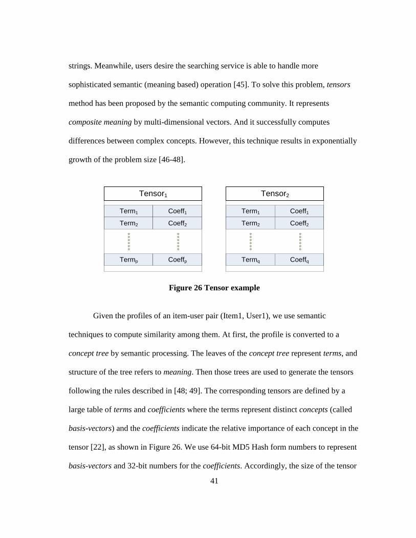
sophisticated semantic (meaning based) operation [45]. To solve this problem, tensors
method has been proposed by the semantic computing community. It represents
composite meaning by multi-dimensional vectors. And it successfully computes
differences between complex concepts. However, this technique results in exponentially
growth of the problem size [46-48].
Term1
Term2
Coeff1
Coeff2
Termp Coeffp
Tensor1
Term1
Term2
Coeff1
Coeff2
Termq Coeffq
Tensor2
Figure 26 Tensor example
Given the profiles of an item-user pair (Item1, User1), we use semantic
techniques to compute similarity among them. At first, the profile is converted to a
concept tree by semantic processing. The leaves of the concept tree represent terms, and
structure of the tree refers to meaning. Then those trees are used to generate the tensors
following the rules described in [48; 49]. The corresponding tensors are defined by a
large table of terms and coefficients where the terms represent distinct concepts (called
basis-vectors) and the coefficients indicate the relative importance of each concept in the
tensor [22], as shown in Figure 26. We use 64-bit MD5 Hash form numbers to represent
basis-vectors and 32-bit numbers for the coefficients. Accordingly, the size of the tensor

42
can become extremely large [46]. More details can be found in our previous published
work [22].
The similarity between every pair of user-item profiles represented as tensors is
computed in three steps using Semantic Information Filtering. Figure 26 shows two
tensors (T1 and T2) of size p, q. The computation of semantic similarity (s12) between T1
and T2 follows: 1) identify common terms in T1 and T2 (say total k); 2) multiply the
corresponding coefficients of the every common terms to produce k products; and 3) sum
all the k products to yield s12.
If the computation of s12 has high performance and energy efficiency, it produces
large economic benefit and better user experience as web data centers and users are
using similar technique. A traditional sequential processor computes the semantic
similarity in O(pq) time, if applying binary search tree it can become O(plogq). In fact,
people have achieved a time complexity of O(p+q) using Bloom filter [50] technique. A
Bloom filter (BF) is an n-bit long bit-vector. It provides a probabilistic method to fast
compute the intersection of two sets. Hence, the common k terms of T1 and T2 can be
identified quickly using BF. We construct two phases to look for common terms in two
tensors. The first phase called BF set is to insert “1” to m positions in an empty BF based
on the given indices. The term values of one tensor pass throughput several independent
hash functions respectively to obtain those indices. Once the insertion completes, the
second phase, BF test, takes each term values in another tensor to compare its
corresponding positions in BF whether or not are “1”. The positions are also generated
using the same hash functions. If all are “1”, we consider the corresponding term value is

43
common between the two tensors. The BF set and BF test can be performed in parallel
(every processing element processes different term values) using a shared BF. Once the
common terms are identified, the products and sum operations of semantic similarity can
be computed easily.
IV.2.2 SoC Design for Semantic Information Filtering
In last section, we discuss the computation process of Semantic Information
Filtering (SIF). This section describes how we use the proposed reconfigurable
computing platform to parallelize the SIF process.
As shown in Figure 27, our SoC design for SIF contains an ARM Cortex A9, an
Execution Controller, RPE matrix with 128 units, a BF-Sync module with 32 AXI Slave
interfaces, a RPE-BF interconnect network, Memory-core interconnect network, CAM-
core interconnect network, RAM units and CAM units.
The ARM Cortex A9 is a low-power RISC processor. In our system, its clock
runs at 1GHz. It initializes the operation of the system, distributes data to the RAM and
CAM units, handles the interrupts from the Execution Controller (EC) and performs the
final sum operations. The input tensor data (Tensor1 and Tensor2) are partitioned into the
RAM units via the DMA Controller. Only the terms of Tensor1 is loaded into the RAM
units whereas the entire Tensor1 is load into the CAM units. The terms and coefficients
of Tensor2 both are written to the RAM units following the Tensor1’s data. At the
moment when all the operations of participating RPE complete, the CPU gets activated
by receiving an interrupt from the EC. It then fetches the partial sums from the RPE and

44
computes the s12 (similarity between Tensor1 and Tensor2) via accumulating the received
sums.
DRAM Bank1
Me
mo
ry-C
ore
In
terc
on
ne
ct
Ne
two
rk
Exe
cu
tio
n C
on
tro
ller
DRAM Bank2
DRAM Bank3
DRAM Bank4
DRAM Bank5
DRAM Bank r
ARM Cortex A9 HDD Controller DMA Controller
System BUS
CAM Bank1
CA
M-C
ore
In
terc
on
ne
ct N
etw
ork
CAM Bank2
CAM Bank3
CAM Bank4
CAM Bank5
CAM Bank s
BF-Sync
AXI Master
RPE0
AXI Master 1
AXI Master 2
AXI Master 3
AXI Slave
RPE-BF Interconnect Network
RPE1
AXI Master 1
AXI Master 2
AXI Master 3
AXI Slave
RPE63
AXI Master 1
AXI Master 2
AXI Master 3
AXI Slave
RPE64
AXI Master 1
AXI Master 2
AXI Master 3
AXI Slave
RPE65
AXI Master 1
AXI Master 2
AXI Master 3
AXI Slave
RPE66
AXI Master 1
AXI Master 2
AXI Master 3
AXI Slave
RPE127
AXI Master 1
AXI Master 2
AXI Master 3
AXI Slave
RPE128
AXI Master 1
AXI Master 2
AXI Master 3
AXI Slave
AXI Master
AXI Master
AXI Master
RPE0
RPE1
RPE128
RPE0
RPE1
RPE128
RPE0 RPE1 RPE128
Figure 27 Proposed reconfigurable SoC for SIF
The Execution Controller (EC) configures RPEs, monitors RPE’s computing
process, and notifies the host core when RPEs complete the desired tasks. First, it
initializes RPEs with the BF set phase configuration so that the RPEs execute the BF set
logic (details are provided in the latter description of RPEs). A complete signal is
received if RPEs finish the execution. Second, the EC sends the BF test phase instruction

45
to the RPEs. This time they enther the BF test phase. The EC waits for the complete
signals for the BF test phase from the RPEs. Finally, it retrieves all the partial sums from
the terminated RPE and then generates an interrupt to the host processor.
RPE State Registers
AXI Master
subcomponent
(Port 1)
To Interconnect 2
Memory Bank
AXI Slave
subcomponent
1.Load processing data
Config Registers
Operation done
To BF-Sync module
From BF-Sync module
32
To Interconnect 3
BF-Sync module
2. Calculate BF index
3.Set Bloom Filter
4. Test Bloom Filter
5. Calculate local SUM s12
Test_success
Test_valid
AXI Master
subcomponent
(Port 2)
AXI Master
subcomponent
(Port 3) To Interconnect 4
CAM Bank
Figure 28 Reconfigurable Processing Element (RPE) for SIF
A Reconfigurable Processing Element (RPE) contains 5 computation logics for
two phases: BF set and BF test. The logics are shown in Figure 28 which is an overview
of a RPE. It has 4 communication ports: one AXI Slave interface and 3 AXI Master
interfaces. The operation 1, Load processing data, loads data from the RAM units via
Port 1. The operation 2, Calculate BF index, generates the indices for BF using 7
independent hash functions for a given input. The operation 3, Set Bloom Filter, sends
the generated BF indices through an AXI Master (Port 2) to the BF-Sync module. The
operation 4, Test Bloom Filter, asks BF-Sync module to check whether a new group of
generated BF indices is presented in the BF. This request is also carried by the Port 2.

46
But the test result is directly given by Test_success and Test_valid from the BF-Sync
module. Test_valid indicates the result is ready and Test_success means we find a term
match. The operation 5 is associated with the operation 4. Once a RPE receives a
positive answer from Test Bloom Filter, the RPE looks for the corresponding coefficient
of Tensor1 in the CAM units. The last AXI Master (port 3) involves in this
communication. During the BF set phase, each RPE executes 1, 2 and 3 serially. Once
the set phase of all RPEs completes, operation 1, 2, 4 and 5 are executed serially.
BF-Sync module (Figure 29) consists of the Bloom Filter (an n-bit vector), the
control logic, 32 AXI Slave interfaces, and 128 pairs of Test_valid and Test_success.
The control logic performs the insertion of the BF and the test of presence using the data
from the AXI Slave ports. It is noticed that the number of AXI Slave ports of the module
may be less than the number of RPEs. Hence, a network is required to enable the
communication between RPEs and BF-Sync. Our VPNoC is the solution. Without the
VPNoC, we are not able to complete the SoC design of the application. Obviously, the
number of AXI Slave interfaces can be determined according to the performance
requirement and the power & area limitation.
RPE-BF interconnect network is our virtual prototype of Network-on-Chip
(VPNoC) component. The network employs static XY routing algorithm and mesh
topology.
Memory-Core interconnect network and CAM-Core interconnect network are
simple crossbar network. As each RAM unit and CAM unit are assigned to a single RPE,

47
using crossbar can reduce the complexity of the system development, and doesn’t affect
the correctness of the evaluation.
1 1 1 0 0 1 1 1 0 0
1 1 1 0 1 1 0 1 0 0
1
1
0
1...
...
...
BF-Sync
Control logic
BF
Test_success1
Test_valid1
Test_success128
Test_valid128
.....
AXI
Slave 1
AXI
Slave 32
Figure 29 BF-Sync module
IV.2.3 System Performance Analysis
Because of the need to observe the RPE in the context of a data-intensive
application and its complexity, we have created a full SoC virtual prototype using
Carbon Model Studio and Carbon SoC Designer. We measure computation time,
communication time and overall execution time for the SIF design on Carbon SoC
Designer simulator. The experiments focus on a single semantic comparison. For the
demonstrative purpose, the computing platform has used three different numbers of
RPEs, e.g. 32, 64 & 128, to process Tensor size of 160k. The similarity is 10%.
In the previous sections, we have mentioned that there is set phase and test phase
in the SIF algorithm. Figure 30 shows the averaged overall and two phases execution
time. Core Active (Set) refers to the time a RPE doing the actual computation during the
set phase; Core Active (Test) is for test phase. Core Stall (Mem read) indicates the
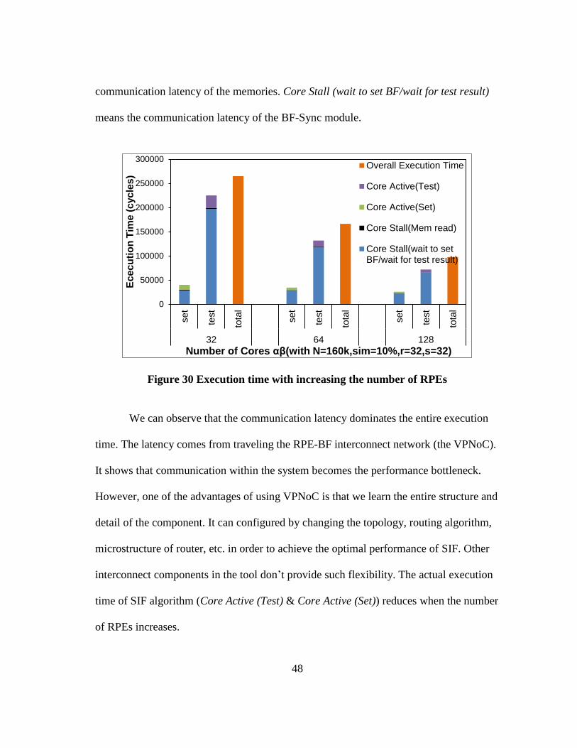
48
communication latency of the memories. Core Stall (wait to set BF/wait for test result)
means the communication latency of the BF-Sync module.
Figure 30 Execution time with increasing the number of RPEs
We can observe that the communication latency dominates the entire execution
time. The latency comes from traveling the RPE-BF interconnect network (the VPNoC).
It shows that communication within the system becomes the performance bottleneck.
However, one of the advantages of using VPNoC is that we learn the entire structure and
detail of the component. It can configured by changing the topology, routing algorithm,
microstructure of router, etc. in order to achieve the optimal performance of SIF. Other
interconnect components in the tool don’t provide such flexibility. The actual execution
time of SIF algorithm (Core Active (Test) & Core Active (Set)) reduces when the number
of RPEs increases.
0
50000
100000
150000
200000
250000
300000
set
test
tota
l
set
test
tota
l
set
test
tota
l
32 64 128
Ec
ec
uti
on
Tim
e (
cyc
les
)
Number of Cores αβ(with N=160k,sim=10%,r=32,s=32)
Overall Execution Time
Core Active(Test)
Core Active(Set)
Core Stall(Mem read)
Core Stall(wait to setBF/wait for test result)

49
IV.3 Collaborative Filtering Recommendation Systems
IV.3.1 Introduction of Recommendation Systems
Nowadays, recommendation systems are widely used in many websites such as
YouTube, Amazon, Netflix, etc. It can follow the steps of its user, observe the interests
of a group of similar users and pick items that best suit the user based on either items the
user liked (content-based filtering) or implicit observations of the user’s
followers/friends who have similar tastes (collaborative filtering). Most of
recommendation systems today employ collaborative filtering (CF) approach as it is
domain-free and easy to collect new user-item relation from user history (e.g.
preferences, ratings etc.) [51]. On the other hand, addition information is required for
content-based filtering. And it may not be found in every application domain.
Figure 31 Computation process of a collaborative filtering recommendation system
CF approach is described in 4 stages, as shown in Figure 31. First, user
preference information is explicitly and implicitly collected by those operating
recommendation systems. Explicit data collection may let a user to rate for the items he
has seen/bought. Implicit method may use the data from items placed on a wish list,
items seen, search made etc. A profile of user-preferences can be built on the data
collected in a recommendation system. In our study, we use generated data, (uID, iID,
collect user perference
calculate item-item pair similarity
compute predictions for
a user
identify top-k recommended
items

50
rate), as the collected information, where uID is the unique id of a user, iID is the id of
an item and rate represents the rating of the item given by the user. rate is in the range of
1 to 5.
ru2
rui
1 2 u.. .. v n..
1
2
i
..
j
m
....
rvj
Users
Ite
ms
unrated ratedusers rated
both items i & j
Figure 32 m x n item-user matrix
Second, CF approach calculates the similarity between all item-item pairs. Given
a set of n different users , a set of m distinct items ,
rui represents the rate that user assigns for the item . In a realistic situation, it
is very likely that users do not rate for all items. Therefore, if a user does not rate for an
item, we still regard this item is rated by this user, but with a rate of 0. Figure 32 visually
shows the relationship between u, i, and rui using a matrix. We compute the
similarity between two items using Pearson’s correlation coefficient [23]. It can
be defined as Equation (3) where sij denotes the similarity metric, Uij is the subset of
users who have rated for item i and item j, and ̅ ( ̅) refers to the average rating of the

51
item i (j). It is obvious that . indicates that all users who have rated
both item i and j have the same opinion, and when they always disagree with
each other. All sij forms a similarity matrix as known in Figure 33. Since each sij can be
independently computed, we easily parallelize this step via assigning computations of sij
to numerous processing units.
∑ ( ̅)( ̅)
√∑ ( ̅) √∑ ( ̅)
(3)
Third, the predictions for the unrated items of a user are computed in this stage.
Given an item i that user u has not seen, the prediction pui that the rating u will give i is
calculated using the multiplication of row i of the similarity matrix and column u of the
item-user matrix. Figure 33 shows the above computation process.
Finally, the top “K” entries among the predicted items are selected to present to
the user.
In this section, we have discussed the computation process of Collaborative
Filtering (CF). The next section describes how we use the proposed reconfigurable
computing platform for CF recommendation system.

52
sij
1 2 i.. .. j m..
Items
1
2
i
..
j
m
....
Ite
ms
1
2
i
..
j
m
....
Ite
ms
u
1
2
i
..
j
m
....
Ite
ms
u
=X
unrated
rated
predicted
similarity matrix
pui
Figure 33 Prediction computation for user u
IV.3.2 SoC Design for Collaborative Filtering Recommendation Systems
People have study CF problem applying MapReduce scheme on traditional
clusters [52; 53] . In [23], they designed a CF recommender with MapReduce
programming paradigm on Intel SCC platform, an experimental 48-core on chip
architecture, and obtained ~2x speedup as compared to those clusters. As the successful
experience of applying the proposed architecture (mentioned in IV.1 section) for
Semantic Information Filtering, can we also take advantages of the architecture in CF
problem? To the best of our knowledge, it is the first time to apply Network-on-Chip for
the design of CF recommendation system.
As shown in Figure 34, our SoC design for CF contains an ARM Cortex A9, an
Execution Controller, Recommender Core (RC) matrix, a Memory-Core interconnect
network, and DRAM units.

53
DRAM Bank1
Me
mo
ry-C
ore
In
terc
on
ne
ct
Ne
two
rk
Exe
cu
tio
n C
on
tro
lle
r
DRAM Bank2
DRAM Bank3
DRAM Bank4
DRAM Bank5
DRAM Bank r
ARM Cortex A9 HDD Controller DMA Controller
System BUS
AXI Master
RC1
AXI Master 1AXI Slave
RC2
AXI Master 1AXI Slave
RCn/2-1
AXI Master 1AXI Slave
RCn/2
AXI Master 1AXI Slave
RCn/2+1
AXI Master 1AXI Slave
RCn/2+2
AXI Master 1AXI Slave
RCn-1
AXI Master 1AXI Slave
RCn
AXI Master 1AXI Slave
AXI Master
AXI Master
AXI Master
RC1
RC2
RCn
Figure 34 Proposed reconfigurable SoC for CF
The ARM Cortex A9 is a low-power RISC processor. In our system, its clock
runs at 1GHz. It initializes the operation of the system, distributes data to the DRAMs,
handles the interrupts from the Execution Controller (EC) and retrieves the top-K
recommended items for users from the DRAMs. The data contained numerous entries
formatted (uID, iID, rate) are partitioned into the RAM units via the DMA Controller.
At the moment when all the operations of participating RCs complete, the CPU gets
activated by receiving an interrupt from the EC. It then fetches the recommended items
for a user from the DRAMs.
The Execution Controller (EC) configures RCs, monitors RC’s computing
process, and notifies the host core when RCs complete the desired tasks. The entire
computation process involves in 4 stages: group operation, correlation coefficient,
matrix multiplication and sort (more details can be found in the latter introduction of

54
RCs). The EC initializes RCs with the corresponding instruction at the beginning of each
stage. A complete signal is received if a RC finishes an execution.
A Recommender Core (RC) is a Reconfigurable Processing Element and
contains 4 computation logics. The logics are shown in Figure 35 which is an overview
of a RC. The AXI Slave subcomponent receives instructions from EC and writes to the
Config Registers. Then the RC State Registers indicate an operation that the RC is going
to execute. The data required at each operation comes from the DRAMs via the AXI
Master subcomponent. The following introduces the intention of each operation.
RC State Registers
AXI Master
subcomponent
To Interconnect
Memory Bank
AXI Slave
subcomponent
Execution
Controller1. group operation
Config Registers
Operation done
322. correlation coefficient
3. matrix multiplication
4. sort
Figure 35 Recommender Core (RC) for CF
At the very beginning, we only know the number of entries of the data needed to
process. The group operation first computes the number of users and number of
items. It then rearranges the data as known in Figure 36. If a user does not rate
for an item, we will assign the rating of 0.
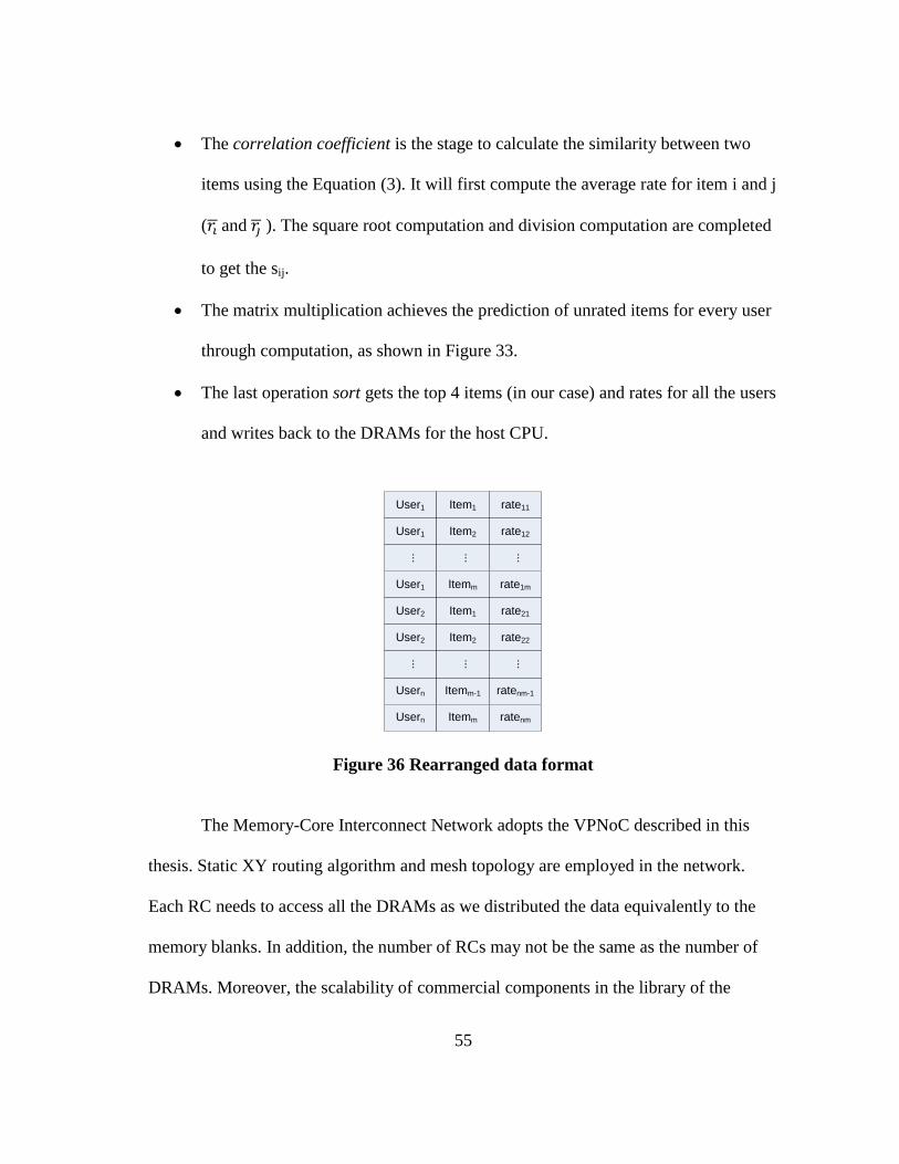
55
The correlation coefficient is the stage to calculate the similarity between two
items using the Equation (3). It will first compute the average rate for item i and j
( ̅ and ̅ ). The square root computation and division computation are completed
to get the sij.
The matrix multiplication achieves the prediction of unrated items for every user
through computation, as shown in Figure 33.
The last operation sort gets the top 4 items (in our case) and rates for all the users
and writes back to the DRAMs for the host CPU.
User1 Item1 rate11
User1 Item2 rate12
User1 Itemm rate1m
...
User2 Item1 rate21
User2 Item2 rate22
Usern Itemm-1 ratenm-1
Usern Itemm ratenm
...
...
...
...
...
Figure 36 Rearranged data format
The Memory-Core Interconnect Network adopts the VPNoC described in this
thesis. Static XY routing algorithm and mesh topology are employed in the network.
Each RC needs to access all the DRAMs as we distributed the data equivalently to the
memory blanks. In addition, the number of RCs may not be the same as the number of
DRAMs. Moreover, the scalability of commercial components in the library of the

56
simulation tool does not allow the system to achieve the expected behavior. Considering
the above reasons, VPNoC is the best suitable interconnection component in our
simulation environment.
IV.3.3 System Performance Analysis
In this section, we have conducted the experiments to evaluate the performance
of our proposed architecture. We can change (1) size of the input data, (2) number of
RCs and number of memory blanks in the evaluation of the system. Our goal is to
demonstrate that the reconfigurable computing platform can perform collaborative
filtering using a traditional approach and obtain the speedup and energy saving with
reference to the state-of-the-art.
The system has been developed and tested in Carbon SoC Designer. It ran at
500MHz clock speed. We applied various sizes of dataset using 32 RCs and 32 memory
blanks. The configurations of (16 RCs, 16 memory blanks) and (64 RCs, 64 memory
blanks) were tested also respectively with 128 users and 256 items dataset. To verify that
our architecture works on practical datasets, the Movielens [54] consisting of 100k
ratings was used in the system configured with 8 RCs and 8 memory blanks, as in [23]
their result was performed using 8 cores.
We measure communication time and computation time for each experiment.
Figure 37 - Figure 39 shows the times for the system configured with 32RCs and 32
memory blanks using a synthetic dataset while increasing number of items. Since we
used brute-force algorithm to compute CF, it is possible to calculate the relationship

57
between number of items and execution time. As shown in Figure 40, our result is
almost the same as the ideal curve.
Figure 37 Execution time for different items size on the 32RCs 32 Mem system
Figure 38 Computation time for
different items size on the 32RCs 32
Mem system
Figure 39 Communication time for
different items size on the 32RCs 32
Mem system
0100200300400500600700800
64I 128I 256I 512I
64U 64U 64U 64U
Tim
e(m
s)
#Item #User
Execution time
0
2
4
6
8
10
12
14
64I 128I 256I 512I
64U 64U 64U 64U
Tim
e(m
s)
#Item #User
Computation time
0
100
200
300
400
500
600
700
64I 128I 256I 512I
64U 64U 64U 64U
Tim
e(m
s)
#Item #User
Communication time

58
Figure 40 Comparison of ideal result and proposed result (normalized)
Figure Figure 41 – Figure 43 demonstrates the performance of different hardware
configurations for 128 Users and 256 Items synthetic dataset. Using more hardware
resource, we were able to gain the speedup accordingly. We cannot go beyond 64RCs
and 64 Memory blanks due to the slow simulation speed, as shown in Table 7.
Table 7 Simulation speed
16 RCs 16 Mems 32 RCs 32 Mems 64 RCs 64 Mems
speed (cycles/sec) 1500 750 350
Applying the practical Movielens-100k dataset (1000 distinct users and 1700
distinct items) on 8 RCs 8 Mems system, it took 273s to complete the computation of
similarity of all item-item pairs, which is better than the result from the state-of-the art.
Intel’s SCC needed 350.2s and cluster service that employed Hadoop required 800s [23].
Both of them were configured with 8 cores and used MapReduce scheme.
0
10
20
30
40
50
60
70
64I 128I 256I 512I
64U 64U 64U 64U
Axi
s Ti
tle
#Item #User
ideal
proposed

59
Figure 41 Execution time for different configurations
Figure 42 Computation time for
different configurations
Figure 43 Communication time for
different configurations
0
100
200
300
400
500
600
16 RC 32 RC 64 RC
16 Mem 32 Mem 64 Mem
Tim
e(m
s)
#cores #memory
Execution time
0
2
4
6
8
10
12
14
16 RC 32 RC 64 RC
16 Mem 32 Mem 64 Mem
Tim
e(m
s)
#cores #memory
Computation time
0
100
200
300
400
500
600
16 RC 32 RC 64 RC
16 Mem 32 Mem 64 Mem
Tim
e(m
s)
#cores #memory
Communication time

60
CHAPTER V
CONCLUSION AND FUTURE WORK
V.1 Conclusion
The increasing complexity of SoC design requires the verification of system
architecture as early as possible during the development process to avoid over-design or
under-design to meet system specification. As the number of component placed on a
single chip continues to grow, handling communication among them becomes a
challenge. Although researchers have proposed Network-on-Chip to solve the on chip
communication issue, designers are not able to use their result directly at the early design
stage. In this thesis, a virtual prototype of scalable NoC for complex SoC design has
been developed to address the above issues. First, RTL model of NoC components
including the router and the CNI have been implemented using Verilog. Then, a virtual
prototype of mesh NoC is constructed in an industrial standard SoC development
platform. A performance evaluation system of NoC is also given to measure the
throughput and latency for different sizes of network under various traffic patterns with
different injection rates. We have applied several workload conditions as well.
The simulation result has demonstrated the scalability of the VPNoC. By
changing the sizes of network, the packets in a larger network experience larger latency.
And a larger network can deliver more packets. We have obtained the consistent result
using all traffic patterns. Moreover, the VPNoC has behaved properly while changing
the workload (number of traffic generators).

61
Finally, we have applied the VPNoC for two data intensive applications. We are
able to complete the proposed reconfigurable computing platform because of utilization
of VPNoC. The interconnect component plays an essential role in the system. For the
collaborative filtering recommendation system, we have demonstrated the system is
scalable and it can achieve a better performance compared with current literature. In
addition, the VPNoC can help us to evaluate the SoC design more precisely as it is a
feasible cycle accurate component.
V.2 Future Work
The next goal of this study is to develop a Fast Model of NoC. A fast model has
better simulation speed but sacrificing the accuracy. In the evaluation of the network, the
simulation time of a bigger size network has increased significantly. Therefore, a
balance between speed and accuracy is needed especially when it is employed to a
complex SoC design.
We also can optimize CNI design and add more service on it (e.g. security, fault
tolerance, etc.). The designers will know the impact to the system after adding new
service at the early development stage of SoC design. It is desired to have the
implementations of adaptive routing algorithms and different topologies.
For the CF application, although we currently only use a brute-force method to
compute the recommended items for users using the proposed reconfigurable
architecture, we still have obtained a promising result. It will be interesting to see if we
map the MapReduce scheme to our platform for CF.

62
REFERENCES
1. Edenfeld, D., Kahng, A. B., Rodgers, M., & Zorian, Y. (2004). Technology
roadmap for semiconductors. Computer, 37(1), 47-56.
2. Bjerregaard, T., & Mahadevan, S. (2006). A survey of research and practices of
network-on-chip. ACM Computing Surveys (CSUR), 38(1), 1-51.
3. Benini, L., & De Micheli, G. (2002). Networks on chips: a new SoC paradigm.
Computer, 35(1), 70-78.
4. Guerrier, P., & Greiner, A. (2000). A generic architecture for on-chip packet-
switched interconnections. In the Proceedings of the Conference on Design,
Automation and Test in Europe, Paris, France (pp. 250-256).
5. Bhojwani, P., & Mahapatra, R. N. (2006). Core Network Interface architecture
and latency constrained on-chip communication. In the Proceedings of the 7th
International Symposium on Quality Electronic Design, San Jose, CA (pp. 358-
363).
6. Duato, J., Yalamanchili, S., & Ni, L. M. (2003). Interconnection networks: an
engineering approach. San Francisco, CA: Morgan Kaufmann.
7. Silburt, A., Perryman, I., Bergeron, J., Nichols, S., Dufresne, M., & Ward, G.
(1995). Accelerating concurrent hardware design with behavioural modelling and
system simulation. In the Proceedings of the 32nd ACM/IEEE Design
Automation Conference, San Francisco, CA (pp. 528-533).
8. De Michell, G., & Gupta, R. K. (1997). Hardware/software co-design.
Proceedings of the IEEE, 85(3), 349-365.
9. Holzer, M., Knerr, B., Belanovic, P., Rupp, M., & Sauzon, G. (2004). Faster
complex SoC design by virtual prototyping. In the International Conference on
Cybernetics and Information Technologies, Systems, and Applications, New
Orlando, FL (pp. 305-309).
10. Schutter, T. D. (2013). The power of developing hardware and software in
parallel: how virtual prototypes reduce risk in a high-stakes game. Available
from http://www.design-reuse.com/articles/31951/the-power-of-developing-
hardware-and-software-in-parallel.html
11. Lavina, J. (2010). Nirgam. Available from http://nirgam.ecs.soton.ac.uk
12. Palesi, M., Patti, D., & Fazzino, F. (2010). Noxim. Available from
http://noxim.sourceforge.net/

63
13. Kumar, A., Agarwal, N., Peh, L.-S., & Jha, N. K. (2008). A system-level
perspective for efficient NoC design. In the IEEE International Parallel and
Distributed Processing, Miami, FL (pp. 1-5).
14. Lu, Z., Thid, R., Millberg, M., Nilsson, E., & Jantsch, A. (2005). NNSE: nostrum
network-on-chip simulation environment. In the Processing Swedish System-on-
Chip Conference, Tammsvik, Sweden (pp. 1-4).
15. Mandal, S. K., Gupta, N., Mandal, A., Malave, J., Lee, J. D., & Mahapatra, R.
(2009). NoCBench: a benchmarking platform for network on chip. In the
Workshop on Unique Chips and Systems, Boston, MA.
16. Arteris Inc. (2013). Arteris FlexNoC interconnect IP. Available from
http://www.arteris.com/flexnoc
17. Carbon Design Systems. (2002). Carbon SoC designer. Available from
http://www.carbondesignsystems.com/
18. Martin, M. M., Sorin, D. J., Beckmann, B. M., Marty, M. R., Xu, M.,
Alameldeen, A. R., . . . Wood, D. A. (2005). Multifacet's general execution-
driven multiprocessor simulator (GEMS) toolset. ACM SIGARCH Computer
Architecture News, 33(4), 92-99.
19. ARM Ltd. (2013). ARM CoreLink NIC-400 network interconnect. Available
from http://www.arm.com/products/system-ip/interconnect/axi/
20. Jung, E. B., Cho, H. W., Park, N., & Song, Y. H. (2006). Sona: an on-chip
network for scalable interconnection of amba-based ips. In the International
Conference on Computational Science, Reading, Berkshire, United Kingdom (pp.
244-251).
21. Dally, W. J., & Seitz, C. L. (1987). Deadlock-free message routing in
multiprocessor interconnection networks. Computers, IEEE Transactions on,
100(5), 547-553.
22. Tripathy, A., Ieong, K. C., Patra, A., & Mahapatra, R. (2013). A reconfigurable
computing architecture for semantic information filtering. In the IEEE
International Conference on Big Data, Santa Clara, CA (pp. 212-218).
23. Tripathy, A., Patra, A., Mohan, S., & Mahapatra, R. (2012). Designing a
collaborative filtering recommender on the single chip cloud computer. In the
High Performance Computing, Networking, Storage and Analysis, Salt Lake City,
UT (pp. 838-847).

64
24. Kumar, S., Jantsch, A., Soininen, J.-P., Forsell, M., Millberg, M., Oberg, J., . . .
Hemani, A. (2002). A network on chip architecture and design methodology. In
the IEEE Computer Society Annual Symposium on VLSI, Pittsburgh, PA (pp.
105-112).
25. Dally, W. J., & Towles, B. (2001). Route packets, not wires: on-chip
interconnection networks. In the Proceedings of Design Automation Conference,
Las Vegas, NV (pp. 684-689).
26. Dally, W. J., & Seitz, C. L. (1986). The torus routing chip. Distributed
computing, 1(4), 187-196.
27. Karim, F., Nguyen, A., & Dey, S. (2002). An interconnect architecture for
networking systems on chips. Micro, IEEE, 22(5), 36-45.
28. Pande, P. P., Grecu, C., Ivanov, A., & Saleh, R. (2003). Design of a switch for
network on chip applications. In the Proceedings of the International Symposium
on Circuits and Systems, Bangkok, Thailand (pp. 217-220).
29. Pande, P. P., Grecu, C., Jones, M., Ivanov, A., & Saleh, R. (2005). Performance
evaluation and design trade-offs for network-on-chip interconnect architectures.
Computers, IEEE Transactions on, 54(8), 1025-1040.
30. Dally, W. J. (1992). Virtual-channel flow control. Parallel and Distributed
Systems, IEEE Transactions on, 3(2), 194-205.
31. Dally, W. J., & Towles, B. P. (2004). Principles and practices of interconnection
networks. San Francisco, CA: Morgan Kaufmann.
32. Hu, J., & Marculescu, R. (2004). DyAD: smart routing for networks-on-chip. In
the Proceedings of the 41st annual Design Automation Conference, San Diego,
CA (pp. 260-263).
33. Daneshtalab, M., Ebrahimi, M., Liljeberg, P., Plosila, J., & Tenhunen, H. (2012).
Memory-efficient on-chip network with adaptive interfaces. Computer-Aided
Design of Integrated Circuits and Systems, IEEE Transactions on, 31(1), 146-
159.
34. Radulescu, A., Dielissen, J., Pestana, S. G., Gangwal, O. P., Rijpkema, E.,
Wielage, P., & Goossens, K. (2005). An efficient on-chip NI offering guaranteed
services, shared-memory abstraction, and flexible network configuration.
Computer-Aided Design of Integrated Circuits and Systems, IEEE Transactions
on, 24(1), 4-17.

65
35. Bhojwani, P., & Mahapatra, R. (2003). Interfacing cores with on-chip packet-
switched networks. In the Proceedings of the 16th International Conference on
VLSI Design, New Delhi, India (pp. 382-387).
36. ARM Ltd. (2003). AMBA AXI Protocol Specification. Available from
http://www.arm.com/products/system-ip/amba/amba-open-specifications.php
37. Mullins, R., West, A., & Moore, S. (2004). Low-latency virtual-channel routers
for on-chip networks. ACM SIGARCH Computer Architecture News, 32(2), 188-
197.
38. Synopsys Inc. (2013). Synopsys platform architect. Available from
http://www.synopsys.com/Systems/ArchitectureDesign/Pages/PlatformArchitect.
aspx
39. Panda, P. R. (2001). SystemC-a modeling platform supporting multiple design
abstractions. In the Proceedings of the 14th International Symposium on System
Synthesis, Montréal, Québec, Canada (pp. 75-80).
40. Gantz, J., & Reinsel, D. (2011). Extracting value from chaos. IDC iView, 1-12.
41. Mitchell, J., & Lapata, M. (2008). Vector-based models of semantic composition.
In the ACL, Columbus, OH (pp. 236-244).
42. Oracle. (2008). Oracle information architecture: an architect's guide to big data.
Available from http://www.oracle.com/technetwork/topics/entarch/articles/oea-
big-data-guide-1522052.pdf
43. IBM Systems and Technology Group. (2011). Dealing with the massive data
generated by many-core systems. Available from
http://www.bscmsrc.eu/sites/default/files/media/bsc-workshop-grice.pdf
44. Kim, Y., Mahapatra, R. N., Park, I., & Choi, K. (2009). Low power
reconfiguration technique for coarse-grained reconfigurable architecture. Very
Large Scale Integration (VLSI) Systems, IEEE Transactions on, 17(5), 593-603.
45. Juan Carlos Perez. (2009). Google joins crowd, adds semantic search capabilities.
Available from
http://www.computerworld.com/s/article/9130318/Google_joins_crowd_adds_se
mantic_search_capabilities_
46. Tripathy, A., Mohan, S., & Mahapatra, R. (2011). Optimizing a semantic
comparator using CUDA-enabled graphics hardware. In the 5th IEEE
International Conference on Semantic Computing, Palo Alto, CA (pp. 125-132).

66
47. Biswas, A., Mohan, S., & Mahapatra, R. (2009). Search co-ordination by
semantic routed network. In the Proceedings of 18th Internatonal Conference on
Computer Communications and Networks, San Francisco, CA (pp. 1-7).
48. Biswas, A., Mohan, S., Panigrahy, J., Tripathy, A., & Mahapatra, R. (2009).
Representation of complex concepts for semantic routed network. In the
Distributed Computing and Networking, Innsbruck, Austria (pp. 127-138).
49. Biswas, A., Mohan, S., Tripathy, A., Panigrahy, J., & Mahapatra, R. N. (2009).
Semantic key for meaning based searching. In the 3rd IEEE International
Conference on Semantic Computing, Berkeley, CA (pp. 209-214).
50. Broder, A., & Mitzenmacher, M. (2004). Network applications of bloom filters: a
survey. Internet Mathematics, 1(4), 485-509.
51. Jannach, D., Zanker, M., Felfernig, A., & Friedrich, G. (2010). Recommender
systems: an introduction. Cambridge, NY: Cambridge University Press.
52. Schelter, S., Boden, C., & Markl, V. (2012). Scalable similarity-based
neighborhood methods with mapreduce. In the Proceedings of the 6th ACM
Conference on Recommender Systems, Dublin, Ireland (pp. 163-170).
53. Jiang, J., Lu, J., Zhang, G., & Long, G. (2011). Scaling-up item-based
collaborative filtering recommendation algorithm based on hadoop. In the IEEE
World Congress on Services, Washington, D.C. (pp. 490-497).
54. Herlocker, J. L., Konstan, J. A., Borchers, A., & Riedl, J. (1999). An algorithmic
framework for performing collaborative filtering. In the Proceedings of the 22nd
International ACM SIGIR Conference on Research and Development in
Information Retrieval, Berkeley, CA (pp. 230-237).