
A Three-Phase Step-Up DC–DC Converter With a Three-Phase ... · Sérgio Vidal Garcia Oliveira,...
14
IEEE TRANSACTIONS ON INDUSTRIAL ELECTRONICS, VOL. 58, NO. 8, AUGUST 2011 3567 A Three-Phase Step-Up DC–DC Converter With a Three-Phase High-Frequency Transformer for DC Renewable Power Source Applications Sérgio Vidal Garcia Oliveira, Member, IEEE, and Ivo Barbi, Fellow, IEEE Abstract—This paper presents a new three-phase step-up dc–dc converter with a three-phase high-frequency (HF) isolation trans- former in an average current-mode controlled closed loop. This converter was developed for industrial applications where the dc input voltage is lower than the output voltage, for instance, in installations fed by battery units, photovoltaic arrays, or fuel cell systems. The converter’s main characteristics are reduced input ripple current, step-up voltage, HF transformer, reduced output- voltage ripple due to three-pulse output current, and the presence of only three active switches connected to the same reference, this being a main advantage of this converter. By means of a specific switch modulation, the converter allows two operational regions, each one depending upon the number of switches in overlapping conditions—if there are two switches, it is called R 2 region, and if there are three switches, it is called R 3 region. An average current-mode control strategy is applied to input-current and output-voltage regulation. Theoretical expressions and experimen- tal results are presented for a 6.8-kW prototype, operating in the R 2 region, and for a 3.4-kW prototype, operating in the R 3 region, both in continuous conduction mode. Index Terms—Average current-mode control, dc–dc power con- version, dc–dc step-up converter, high-frequency (HF) three-phase transformer, installations fed by dc power sources. I. I NTRODUCTION T HE great necessity in several areas, particularly the in- dustrial sector, for switch mode power converters with larger power ratings in the end of the 80s was the starting point for the appearance of high-frequency (HF) three-phase dc–dc converter. Since the first three-phase dc–dc isolated converter introduced by Prazad et al. in 1988 [1], the three-phase dc–dc development follows two paths, both with the same goal: to increase the electronic power density ratings. The new topolo- gies are from the first path and have important propositions [1]–[9]. The second path is the soft commutation with its main contributions given in [10]–[12]. The typical architecture of an HF three-phase dc–dc isolated converter is shown in Fig. 1. In the input stage, the most Manuscript received July 1, 2009; revised December 4, 2009 and February 12, 2010; accepted March 26, 2010. Date of publication October 7, 2010; date of current version July 13, 2011. This work was supported in part by the Coordenação de Aperfeiçoamento de Pessoal de Nível Superior and in part by the Conselho Nacional de Desenvolvimento Científico e Tecnológico (CNPq). S. V. G. Oliveira is with the Universidade Regional de Blumenau–FURB, Blumenau 89030-000, Brazil (e-mail: sergio_vidal@ ieee.org). I. Barbi is with the Instituto de Eletrônica de Potência, Universidade Fed- eral de Santa Catarina, Florianópolis 88040-970, Brazil (e-mail: ivobarbi@ inep.ufsc.br). Digital Object Identifier 10.1109/TIE.2010.2084971 common configuration is this stage to operate as a voltage source, while the output stage has current source characteristics like in [1], [3], [4], [6], [9], [11], and [12]. The advantages of three-phase dc–dc isolated solutions are as follows: 1) reduction of the input and output filters’ volume, as well as the reduction of weight and size of the isolation transformers; 2) lower rms current levels through the power components, when compared to single-phase solutions for the same power ratings. With the increasing threat of the fast depletion of resources such as petroleum, coal, and natural gas forces, people seek renewable energy sources, such as solar, wind, geothermal, and hydraulic energies. In recent years, fuel cell (FC) research and development have received special attention for their higher energy-conversion efficiency and lower CO 2 emissions than thermal engines in the processes of converting fuel into usable energies. For these systems, different power converter topolo- gies can be used for the power electronic interface between them and the load. Basically, low-voltage high-current struc- tures are needed because of its electrical characteristics. In these systems, a classical boost converter is often selected as a possible converter. However, a classical boost converter will be limited when the power increases (greater than 4.5 kW) or for higher step-up ratios (greater than two times). The major problems of using a single dc/dc converter connected with FC in high-power applications are the difficulty of the design of magnetic component and high FC ripple current, which may lead to the reduction of its stack lifetime. To overcome these limitations, the use of paralleling power converters with interleaved technique is also applied and may offer some better performances [13]–[19]. In industrial applications, the inverter systems, together with dc–dc high-voltage-ratio converters, that feed electrical power from low-voltage-level systems into the grid must convert their direct current into alternating current for the grid. In [20], a study focusing on this, offering a comparative view of some dc–dc converters applied in systems in the medium power range of 20 kW and higher, is presented. The three-phase step-up dc–dc isolated converter presented in this paper, Fig. 2, has all of the main advantages of the three-phase solutions presented up until now. Moreover, the reduced number of switches, if compared with other topologies, such as presented in [21], and the voltage step-up character- istic improve the efficiency and reduce, along with a high 0278-0046/$26.00 © 2010 IEEE
Transcript of A Three-Phase Step-Up DC–DC Converter With a Three-Phase ... · Sérgio Vidal Garcia Oliveira,...

IEEE TRANSACTIONS ON INDUSTRIAL ELECTRONICS, VOL. 58, NO. 8, AUGUST 2011 3567
A Three-Phase Step-Up DC–DC Converter Witha Three-Phase High-Frequency Transformer for
DC Renewable Power Source ApplicationsSérgio Vidal Garcia Oliveira, Member, IEEE, and Ivo Barbi, Fellow, IEEE
Abstract—This paper presents a new three-phase step-up dc–dcconverter with a three-phase high-frequency (HF) isolation trans-former in an average current-mode controlled closed loop. Thisconverter was developed for industrial applications where the dcinput voltage is lower than the output voltage, for instance, ininstallations fed by battery units, photovoltaic arrays, or fuel cellsystems. The converter’s main characteristics are reduced inputripple current, step-up voltage, HF transformer, reduced output-voltage ripple due to three-pulse output current, and the presenceof only three active switches connected to the same reference, thisbeing a main advantage of this converter. By means of a specificswitch modulation, the converter allows two operational regions,each one depending upon the number of switches in overlappingconditions—if there are two switches, it is called R2 region, andif there are three switches, it is called R3 region. An averagecurrent-mode control strategy is applied to input-current andoutput-voltage regulation. Theoretical expressions and experimen-tal results are presented for a 6.8-kW prototype, operating inthe R2 region, and for a 3.4-kW prototype, operating in theR3 region, both in continuous conduction mode.
Index Terms—Average current-mode control, dc–dc power con-version, dc–dc step-up converter, high-frequency (HF) three-phasetransformer, installations fed by dc power sources.
I. INTRODUCTION
THE great necessity in several areas, particularly the in-dustrial sector, for switch mode power converters with
larger power ratings in the end of the 80s was the starting pointfor the appearance of high-frequency (HF) three-phase dc–dcconverter. Since the first three-phase dc–dc isolated converterintroduced by Prazad et al. in 1988 [1], the three-phase dc–dcdevelopment follows two paths, both with the same goal: toincrease the electronic power density ratings. The new topolo-gies are from the first path and have important propositions[1]–[9]. The second path is the soft commutation with its maincontributions given in [10]–[12].
The typical architecture of an HF three-phase dc–dc isolatedconverter is shown in Fig. 1. In the input stage, the most
Manuscript received July 1, 2009; revised December 4, 2009 andFebruary 12, 2010; accepted March 26, 2010. Date of publication October 7,2010; date of current version July 13, 2011. This work was supportedin part by the Coordenação de Aperfeiçoamento de Pessoal de NívelSuperior and in part by the Conselho Nacional de Desenvolvimento Científicoe Tecnológico (CNPq).
S. V. G. Oliveira is with the Universidade Regional de Blumenau–FURB,Blumenau 89030-000, Brazil (e-mail: sergio_vidal@ ieee.org).
I. Barbi is with the Instituto de Eletrônica de Potência, Universidade Fed-eral de Santa Catarina, Florianópolis 88040-970, Brazil (e-mail: [email protected]).
Digital Object Identifier 10.1109/TIE.2010.2084971
common configuration is this stage to operate as a voltagesource, while the output stage has current source characteristicslike in [1], [3], [4], [6], [9], [11], and [12]. The advantages ofthree-phase dc–dc isolated solutions are as follows:
1) reduction of the input and output filters’ volume, aswell as the reduction of weight and size of the isolationtransformers;
2) lower rms current levels through the power components,when compared to single-phase solutions for the samepower ratings.
With the increasing threat of the fast depletion of resourcessuch as petroleum, coal, and natural gas forces, people seekrenewable energy sources, such as solar, wind, geothermal, andhydraulic energies. In recent years, fuel cell (FC) research anddevelopment have received special attention for their higherenergy-conversion efficiency and lower CO2 emissions thanthermal engines in the processes of converting fuel into usableenergies. For these systems, different power converter topolo-gies can be used for the power electronic interface betweenthem and the load. Basically, low-voltage high-current struc-tures are needed because of its electrical characteristics. Inthese systems, a classical boost converter is often selected asa possible converter. However, a classical boost converter willbe limited when the power increases (greater than 4.5 kW) orfor higher step-up ratios (greater than two times). The majorproblems of using a single dc/dc converter connected withFC in high-power applications are the difficulty of the designof magnetic component and high FC ripple current, whichmay lead to the reduction of its stack lifetime. To overcomethese limitations, the use of paralleling power converters withinterleaved technique is also applied and may offer some betterperformances [13]–[19]. In industrial applications, the invertersystems, together with dc–dc high-voltage-ratio converters, thatfeed electrical power from low-voltage-level systems into thegrid must convert their direct current into alternating currentfor the grid.
In [20], a study focusing on this, offering a comparative viewof some dc–dc converters applied in systems in the mediumpower range of 20 kW and higher, is presented.
The three-phase step-up dc–dc isolated converter presentedin this paper, Fig. 2, has all of the main advantages of thethree-phase solutions presented up until now. Moreover, thereduced number of switches, if compared with other topologies,such as presented in [21], and the voltage step-up character-istic improve the efficiency and reduce, along with a high
0278-0046/$26.00 © 2010 IEEE

3568 IEEE TRANSACTIONS ON INDUSTRIAL ELECTRONICS, VOL. 58, NO. 8, AUGUST 2011
Fig. 1. Typical three-phase dc–dc converter architecture.
Fig. 2. Three-phase step-up dc–dc isolated converter.
TABLE IOPERATION REGIONS FOR THE CONVERTER
switching frequency, the output filter volume, respectively.Furthermore, due to the input-current-source characteristic ornonpulsed input current, this topology can be adopted in alltypes of applications supplied by alternative energy sources,such as battery or photovoltaic (PV) arrays and, the more recent,FC systems. In this way, for the proposed converter, threeconverter operation regions are defined, each one dependingupon the number of switches in overlapping conditions, Table I.Theoretical expressions and experimental results are presentedfor a 6.8-kW prototype, operating in region R2, and for a3.4 kW-prototype, operating in region R3, both in continuousconduction mode (CCM).
II. PROPOSED CONVERTER AND
THE OPERATION PRINCIPLE
A. Circuit Description
Fig. 2 shows the power stage of the proposed circuit [7].The left side of the circuit (inverter) comprises three inductors
and three switches connected to a dc link. The right side ofthe circuit is a traditional three-branch six-diode rectifier with acapacitive output filter. An HF three-phase transformer links toboth sides.
The three-phase step-up dc–dc isolated converter character-istics are as follows.
1) The proposed three-phase inverter (left-side) circuitpresents a low input ripple current, because it acts asnonpulsed current source, independent of both operationmodes and regions of the converter.
2) The output-voltage ripple is reduced due to the three-pulse output current; consequently, a small capacitancevalue is required.
3) Only the three switches connected to the same referenceattribute simplicity to the drive and control circuits.
4) The voltage level applied across the switches is reduceddue to the employed transformer.
B. Analysis of Operation
To facilitate the analysis of the circuit operation, Fig. 2 showsa simplified circuit diagram. In the simplified circuit, Tr1 ismodeled as an ideal transformer with turns ratio n = 1. It isassumed that its magnetizing inductance is large enough thatit can be neglected. Moreover, it is assumed that the filtercapacitor C is large enough and, thus, its output-voltage ripple

OLIVEIRA AND BARBI: STEP-UP DC–DC CONVERTER WITH HF TRANSFORMER FOR POWER SOURCE APPLICATIONS 3569
Fig. 3. Power switch driving signals for region R2.
is small compared to its dc voltage. Finally, it is assumedthat all semiconductor components are ideal, i.e., they presentzero impedance when on and infinite impedance when off.The power flux transfer and the output/input voltage ratio arecontrolled by the duty ratio D of the switches.
A PWM technique is used for switches S1, S2, and S3. Theduty ratio D is defined by (1), where tON is the on-time intervalof the switches and TS is the switching period
D =tON
TS. (1)
C. Operation Regions
The circuit proposed has three different operation regionsaccording to Table I. Each one differs from each other bythe number of switches in the ON state at the same time(overlapping). For each region, the duty cycle ratio can assumedifferent values. Due to the converter’s input-current-sourcecharacteristic, at least one switch must always be on. Hence,the first region, R1 is forbidden. Fig. 3 shows a modulation ofthe switches for the converter operation in region R2.
D. Steady-State Stage Operations for Region R2
Fig. 4 shows the six topological stages of the converter’soperation at R2 region during a switching period.
1) First Stage (t0, t1)—Fig. 4(a): In t0, switch S1 is turnedon and conducts along with switch S3. Inductances L1 andL3 store energy from source E. The energy stored in L2 istransferred to the load through D2, D4, and D6. CurrentsiD4(t) and iD6(t) are added to iS1(t) and iS3(t), respectively.This stage finishes in t1 when S3 is turned off.
2) Second Stage (t1, t2)—Fig. 4(b): In t1, S3 is turned off,and the energy stored in L2 and L3 is transferred to the loadthrough D3, D2, and D4. Current iD4(t) is added to iS1(t).This stage finishes in t2 when S2 is turned on.
3) Third Stage (t2, t3)—Fig. 4(c): In t2, the energy ofsource E is stored in inductances L1 and L2. The energy storedin L3 continues to be transferred to the load through D3, D4,and D5. This stage finishes in t3 when S1 is turned off.
4) Fourth stage (t3, t4)—Fig. 4(d): In t3, the energy storedin L1 and L3 is transferred to the load through D1, D3, andD5. Current iD5(t) is added to iS2(t). This stage finishes in t4when S3 is turned on. Fig. 4. Topological stages of the converter in region R2.

3570 IEEE TRANSACTIONS ON INDUSTRIAL ELECTRONICS, VOL. 58, NO. 8, AUGUST 2011
Fig. 5. Power switch driving signals for region R3.
5) Fifth Stage (t4, t5)—Fig. 4(e): In t4, the energy of sourceE is stored in inductances L2 and L3. The energy stored in L1
continues to be transferred to the load through D1, D5, and D6.This stage finishes in t5 when S2 is turned off.
6) Sixth Stage (t5, t6)—Fig. 4(f): The converter’s last stageof operation in a TS switching period starts at t5, when S2 isturned off. The energy from source E stored in inductancesL2 and L1 is then transferred to the load through D1, D2, andD6. iD6(t) is added to switch current iS3(t). In t6, a switchingperiod is finished.
E. Steady-State Stage Operations for Region R3
Fig. 5 shows the modulation of the switches for the con-verter’s operation in region R3. Fig. 6 shows the topologicalstages of the converter’s operation in R3 region.
1) First Stage (t0, t1)—Fig. 6(a): In t0, switch S1 is turnedon and conducts along with switches S2 and S3. InductancesL1, L2, and L3 stored energy from source E. This stage finishesin t1 when S2 is turned off.
2) Second Stage (t1, t2)–Fig. 6(b): In t1, S2 is turned off,and the energy stored in L2 is transferred to the load throughdiodes D2, D4, and D6. Currents iD4(t) and iD6(t) are addedto currents iS1(t) and iS3(t), respectively. This stage finishesin t2 when S2 is turned on.
3) Third Stage (t2, t3)—Fig. 6(a): In t2, S2 is turned on, andthe first stage is repeated, with the energy of the source beingstored in inductances L1, L2, and L3. This stage finishes in t3when S3 is turned off.
4) Fourth Stage (t3, t4)—Fig. 6(c): When S3 is turned off,the energy stored in L3 is transferred to the load through D3,D4, and D5. Currents iD4(t) and iD5(t) are added to switchcurrents iS1(t) and iS2(t), respectively. This stage finishes int4 when S3 is turned on again.
5) Fifth Stage (t4, t5)—Fig. 6(a): In t4, S3 is turned on, andthe first stage is repeated, with the energy off the source beingstored in inductances L1, L2, and L3. This stage finishes in t5when S1 is turned off.
6) Sixth Stage (t5, t6)—Fig. 6(d): The last stage starts at t5,with S1 being turned off and the energy stored in inductance L1
being transferred to the load through diodes D1, D5, and D6.Diode currents iD5(t) and iD6(t) are added to switch currentsiS2(t) and iS3(t), respectively. In t6, one period of switchingoperation is concluded.
Fig. 6. Topological stages of the converter in operational region R3.
III. POWER STAGE DESIGN PROCEDURE
The main equations (2)–(9) are used to design the powerstage of the converter. Equation (2) gives the normalized outputcurrent, and (3) gives the turns ratio. By means of (4) and (5),the designer can determine the minimum value of inductances
OLIVEIRA AND BARBI: STEP-UP DC–DC CONVERTER WITH HF TRANSFORMER FOR POWER SOURCE APPLICATIONS 3571
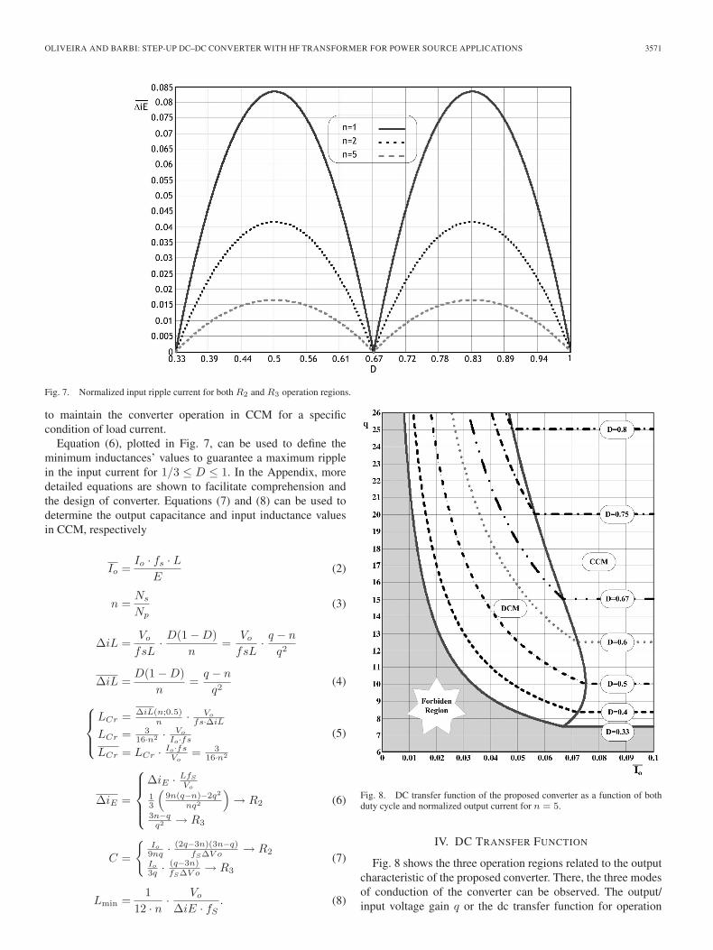
Fig. 7. Normalized input ripple current for both R2 and R3 operation regions.
to maintain the converter operation in CCM for a specificcondition of load current.
Equation (6), plotted in Fig. 7, can be used to define theminimum inductances’ values to guarantee a maximum ripplein the input current for 1/3 ≤ D ≤ 1. In the Appendix, moredetailed equations are shown to facilitate comprehension andthe design of converter. Equations (7) and (8) can be used todetermine the output capacitance and input inductance valuesin CCM, respectively
Io =Io · fs · L
E(2)
n =Ns
Np(3)
ΔiL =Vo
fsL· D(1 − D)
n=
Vo
fsL· q − n
q2
ΔiL =D(1 − D)
n=
q − n
q2(4)
⎧⎪⎨⎪⎩LCr = ΔiL(n;0.5)
n · Vo
fs·ΔiL
LCr = 316·n2 · Vo
Io·fs
LCr = LCr · Io·fsVo
= 316·n2
(5)
ΔiE =
⎧⎪⎪⎨⎪⎪⎩ΔiE · LfS
Vo
13
(9n(q−n)−2q2
nq2
)→ R2
3n−qq2 → R3
(6)
C =
{Io
9nq · (2q−3n)(3n−q)fSΔV o → R2
Io
3q · (q−3n)fSΔV o → R3
(7)
Lmin =1
12 · n · Vo
ΔiE · fS. (8)
Fig. 8. DC transfer function of the proposed converter as a function of bothduty cycle and normalized output current for n = 5.
IV. DC TRANSFER FUNCTION
Fig. 8 shows the three operation regions related to the outputcharacteristic of the proposed converter. There, the three modesof conduction of the converter can be observed. The output/input voltage gain q or the dc transfer function for operation

3572 IEEE TRANSACTIONS ON INDUSTRIAL ELECTRONICS, VOL. 58, NO. 8, AUGUST 2011
area R2 in CCM is limited to a maximum of three times thetransformer’s turns ratio. Otherwise, in region R3, the mini-mum value of the output voltage in CCM is three times thetransformer’s turns ratio. The gain q for the three modes andtwo regions of converter operation is given by (9), detailed inthe Appendix, and is shown in Fig. 8, highlighting that the dutycycle must be higher than 33% for the correct functionality ofthe converter.
Equation (9) was obtained applying the inductor voltage–second balance described in [22] and [23]. Figs. 9 and 10 showthe theoretical waveforms for both regions of operation R2
and R3
q =
⎧⎪⎪⎪⎪⎨⎪⎪⎪⎪⎩qCCM = n
(1
1−D
)qCrCM = 1
4Io
(3 ±
√9 − 24nIo
)qDCM = n + 3
2
(D2
Io
).
(9)
V. CONTROL DESIGN
In this section, the average current-mode control techniqueapplied to the regulation of both input current and outputvoltage of the converter is described [24]. Fig. 11 shows thefeedback loop for input-current and output-voltage regulation.There are two loops, namely, inner current loop and outer volt-age loop. Gi(s) is the control-to-input-current transfer function,where the controlled variable is the input current IE(s) andthe control variable is the duty ratio d(s). Gv(s) is the line-to-output or input-current-to-output-voltage transfer function.Ci(s) and Cv(s) are the current and voltage compensators,respectively. Vref and Iref are the references to be reached.The inner loop imposes an input current IE(s) as a function ofthe reference current generated by the outer loop. The currentcompensation network is designed as a function of the controlcriterion and by the response of the system.
The output-voltage control-loop action must change theinput-current reference slowly, in relation to the current control-loop action in order to avoid the interference of the outer controlloop.
A. Control Design Equations
The control transfer functions Gi(s) and Gv(s) are describedby (10) and (11), respectively. Other modeling equations arepresented at the Appendix
Gi(S) =IE(S)VC(S)
= Gid(S + ωZi)(
S2
ω2o
+ SωoQ + 1
)Gid =
Vo · CVs(1 − D)2
ωZi =2
RC
ωo =(1 − D)√
LCQ =
√L
CR(1 − D) (10)
Gv(S) =Vo(S)IE(S)
= Gvo(S + ωZv)
S(S + ωPv)
Gvo =R · Rse(1 − D)
(R + Rse)nωZv =
1RseC
ωPv =1
(R + Rse)C. (11)
VI. PROTOTYPE DESCRIPTION AND EXPERIMENTATION
The goal of this analysis is to show the advantages of usingthe proposed converter. The experimental results are obtainedfor a system with the following specifications:
1) Po = 3.4 and 6.8 = kW, output power;2) V o = 450 V, rated output voltage;3) E = 27 and 47 V dc, rated input voltages;4) fs = 20 kHz, switching frequency;5) n = 21/4, transformer’s turns-ratio;6) ΔV o ≤ 9 V, output ripple voltage;7) ΔIE ≤ 3 A, input ripple current.
A. DC Voltage Gain
From the output and input rated voltages, the gain q isgiven by
q =450V
47V= 9.57. (12)
B. Duty Ratio
The duty cycle ratio is given by
D =q − n
q=
9.57 − 5.259.57
∼= 0.45. (13)
C. Input Inductances
The values of the inductances were defined, taking intoaccount that the converter keeps operating in CCM, even with10% of the rated power. Under these conditions, the inductancevalues are given by
L1,2,3 ≥ 10LCr ·Vo
fs · Io
∼= 134 μH. (14)
D. Output Capacitance
The value of output capacitance is obtained using (7). How-ever, due to its rms current stress, it was changed to 2000 μF/500 V.
E. Controller Design
The implementation of the compensators for input currentand output voltage is realized by
Ci(S) =Vc(S)
ViHall(S)= Ki
(S + ωZci)S(S + ωPci)
Ki =1
RciC2fi= 555556
OLIVEIRA AND BARBI: STEP-UP DC–DC CONVERTER WITH HF TRANSFORMER FOR POWER SOURCE APPLICATIONS 3573
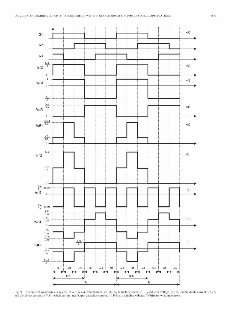
Fig. 9. Theoretical waveforms in R2 for D = 0.5. (a) Command pulses. (b) L1 inductor current. (c) L2 inductor voltage. (d) D1 output diode current. (e) D5
and D6 diode currents. (f) S1 switch current. (g) Output capacitor current. (h) Primary winding voltage. (i) Primary winding current.

3574 IEEE TRANSACTIONS ON INDUSTRIAL ELECTRONICS, VOL. 58, NO. 8, AUGUST 2011
Fig. 10. Theoretical waveforms in R3 for D = 0.83. (a) Command pulses. (b) L1 inductor current. (c) L2 inductor voltage. (d) D1 output diode current.(e) D5 and D6 diode currents. (f) S1 switch current. (g) Output capacitor current. (h) Primary winding voltage. (i) Primary winding current.
OLIVEIRA AND BARBI: STEP-UP DC–DC CONVERTER WITH HF TRANSFORMER FOR POWER SOURCE APPLICATIONS 3575
Fig. 11. Feedback loop for input-current and output-voltage regulation.
ωZi =1
RfiC1fi= 1191
rads
ωPi =(
C1fi + C2fi
C2fi
)ωZi = 100397
rads
(15)
Cv(S) =IRef (S)VvHall(S)
= Kv(S + ωZcv)
S(S + ωPcv)
Kv =1
RcvC2fv= 60.6
ωZcv =1
RfvC1fv= 1250
rads
ωPcv =(
C1fv + C2fv
C2fv
)ωZc = 3230
rads
. (16)
The crossover frequencies obtained from the current controland the voltage control loop are 12.2 and 1.8 kHz, respectively.The crossover frequency must be lower than the switching fre-quency, and a phase margin near to 45◦ provides good responsewith very little output-voltage overshoot. The conventionalphase-margin and gain-margin stability criteria are applied tomaintain the system stable.
F. Prototype Description
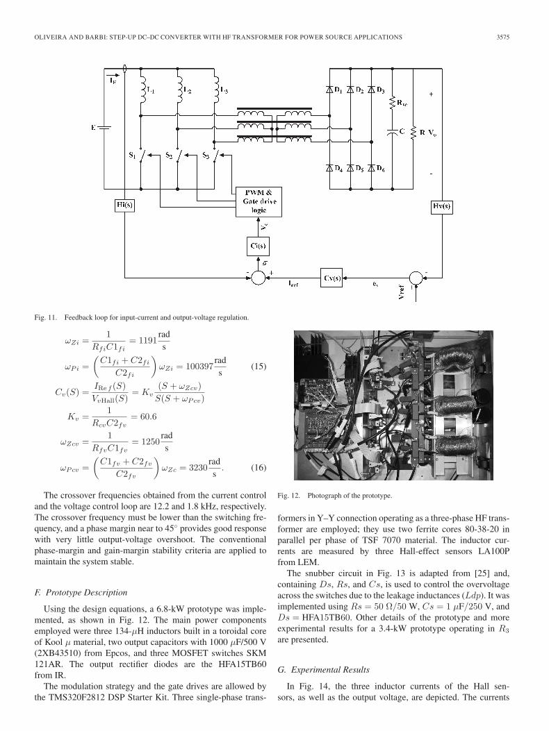
Using the design equations, a 6.8-kW prototype was imple-mented, as shown in Fig. 12. The main power componentsemployed were three 134-μH inductors built in a toroidal coreof Kool μ material, two output capacitors with 1000 μF/500 V(2XB43510) from Epcos, and three MOSFET switches SKM121AR. The output rectifier diodes are the HFA15TB60from IR.
The modulation strategy and the gate drives are allowed bythe TMS320F2812 DSP Starter Kit. Three single-phase trans-
Fig. 12. Photograph of the prototype.
formers in Y–Y connection operating as a three-phase HF trans-former are employed; they use two ferrite cores 80-38-20 inparallel per phase of TSF 7070 material. The inductor cur-rents are measured by three Hall-effect sensors LA100Pfrom LEM.
The snubber circuit in Fig. 13 is adapted from [25] and,containing Ds, Rs, and Cs, is used to control the overvoltageacross the switches due to the leakage inductances (Ldp). It wasimplemented using Rs = 50 Ω/50 W, Cs = 1 μF/250 V, andDs = HFA15TB60. Other details of the prototype and moreexperimental results for a 3.4-kW prototype operating in R3
are presented.
G. Experimental Results
In Fig. 14, the three inductor currents of the Hall sen-sors, as well as the output voltage, are depicted. The currents
3576 IEEE TRANSACTIONS ON INDUSTRIAL ELECTRONICS, VOL. 58, NO. 8, AUGUST 2011
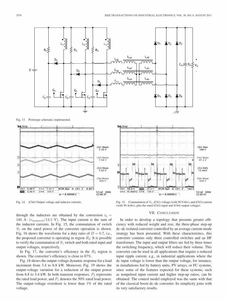
Fig. 13. Prototype schematic implemented.
Fig. 14. (Ch4) Output voltage and inductor currents.
through the inductors are obtained by the conversion iL =100 A · (vsensored/13.5 V). The input current is the sum ofthe inductor currents. In Fig. 15, the commutation of switchS1 on the rated power of the converter operation is shown.Fig. 16 shows the waveforms for a duty ratio of D = 0.7, i.e.,the proposed converter is operating in region R3. It is possibleto verify the commutation of S1 switch and both rated input andoutput voltages, respectively.
In Fig. 17, the converter’s efficiency in the R2 region isshown. The converter’s efficiency is close to 87%.
Fig. 18 shows the output-voltage dynamic response for a loadincrement from 3.4 to 6.8 kW. Moreover, Fig. 19 shows theoutput-voltage variation for a reduction of the output powerfrom 6.8 to 3.4 kW. In both transient responses, P2 representsthe rated load power, and P1 denotes the 50% rated load power.The output-voltage overshoot is lower than 1% of the ratedvoltage.
Fig. 15. Commutation of S1, (Ch1) voltage (with 50 V/div), and (Ch3) current(with 50 A/div), plus the rated (Ch2) input and (Ch4) output voltages.
VII. CONCLUSION
In order to develop a topology that presents greater effi-ciency with reduced weight and size, the three-phase step-updc–dc isolated converter controlled by an average current-modestrategy has been presented. With these characteristics, thisconverter contains only three controlled switches and an HFtransformer. The input and output filters are fed by three timesthe switching frequency, which will reduce their volume. Thisconverter can be used in all applications that require a reducedinput ripple current, e.g., in industrial applications where thedc input voltage is lower than the output voltage, for instance,in installations fed by battery units, PV arrays, or FC systems,since some of the features expected for these systems, suchas nonpulsed input current and higher step-up ratios, can beobtained. The control model employed was the same with thatof the classical boost dc–dc converter. Its simplicity joins withits very satisfactory results.

OLIVEIRA AND BARBI: STEP-UP DC–DC CONVERTER WITH HF TRANSFORMER FOR POWER SOURCE APPLICATIONS 3577
Fig. 16. Experimental results for operational region R3: Commutation of S1,(Ch1) voltage (with 50 V/div) and (Ch3) current (with 50 A/div), plus the rated(Ch2) input and (Ch4) output voltages.
Fig. 17. Output converter’s experimental efficiency on R2.
Fig. 18. Output voltage for an increment of 50% in the output power.
During the converter assembly, special care was taken inthe construction of the transformer, mainly with respect to thereduction of its leakage inductance. This characteristic is animportant constraint for choosing switching frequency.
The obtained efficiency for the converter operating at regionR2 was close to 87%; it can be considered high, consideringits rated power and that it works with hard-switching commu-
Fig. 19. Output voltage for a reduction of 50% in the output power.
tation. With the goal of performing tests in both operationalregions using the same prototype, in region R3, results wereobtained for a 3.4-kW output power and a 27-V input voltagefor the same rated output voltage.
APPENDIX
A. DC Transfer Function
In the following equations, the load variations are repre-sented by means of the normalized output current Io. Accordingto the converter’s operational steps, the average output currentis the sum of the average currents of the diodes (D1, D2, andD3) given by (17). Using (18) and (19), (20), which evaluatesthe average load current, is obtained. From that, the normalizedoutput current Io is obtained by means of (21)
Io = 3ID1 =32iLmax
Δtd
TS(17)
iLmax =V o
fsL· D
q(18)
Δtd =iLmax · n · L
Vo − nE(19)
Io =32· D2
q − n· E
fs · L (20)
Io = Io ·fs · L
E=
32· D2
q − n. (21)
From (21), the dc voltage gain in discontinuous conduc-tion mode (DCM)(qDCM)) can be obtained by means of thefollowing:
qDCM = n +32
(D2
Io
). (22)
In the critical conduction mode (CrCM), i.e., the boundarybetween the CCM and DCM, both qCCM and qDCM are equal,
3578 IEEE TRANSACTIONS ON INDUSTRIAL ELECTRONICS, VOL. 58, NO. 8, AUGUST 2011
and qCrCM is described by means of (23). Thus, (9) synthesizesthe voltage gain relations for all operational modes
qMCC = qMCD
n
1 − D= n +
32· D2
Io
D =qCrCM−n
qCrCM
2Ioq2CrCM−3qCrCM+3n = 0
qCrCM =1
4Io
·(3 ±
√9−24nIo
). (23)
B. Modeling and Control
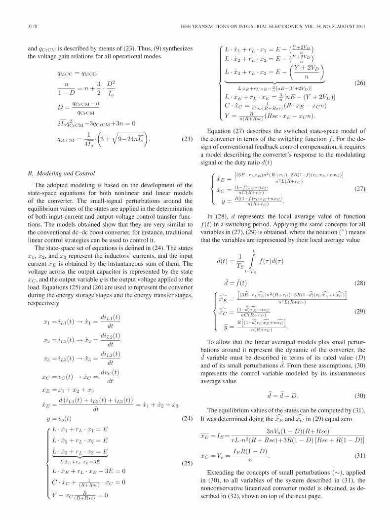
The adopted modeling is based on the development of thestate-space equations for both nonlinear and linear modelsof the converter. The small-signal perturbations around theequilibrium values of the states are applied in the determinationof both input-current and output-voltage control transfer func-tions. The models obtained show that they are very similar tothe conventional dc–dc boost converter, for instance, traditionallinear control strategies can be used to control it.
The state-space set of equations is defined in (24). The statesx1, x2, and x3 represent the inductors’ currents, and the inputcurrent xE is obtained by the instantaneous sum of them. Thevoltage across the output capacitor is represented by the statexC , and the output variable y is the output voltage applied to theload. Equations (25) and (26) are used to represent the converterduring the energy storage stages and the energy transfer stages,respectively
x1 = iL1(t) → x1 =diL1(t)
dt
x2 = iL2(t) → x2 =diL2(t)
dt
x3 = iL3(t) → x3 =diL3(t)
dt
xC = vC(t) → xC =dvC(t)
dt
xE = x1 + x2 + x3
xE =d (iL1(t) + iL2(t) + iL3(t))
dt= x1 + x2 + x3
y = vo(t) (24)⎧⎪⎪⎪⎪⎪⎪⎪⎪⎪⎪⎪⎪⎨⎪⎪⎪⎪⎪⎪⎪⎪⎪⎪⎪⎪⎩
L · x1 + rL · x1 = E
L · x2 + rL · x2 = E
L · x3 + rL · x3 = E︸ ︷︷ ︸L·xE+rL·xE=3E
L · xE + rL · xE − 3E = 0
C · xC + 1(R+Rse) · xC = 0
Y − xCR
(R+Rse) = 0
(25)
⎧⎪⎪⎪⎪⎪⎪⎪⎪⎪⎪⎪⎪⎪⎨⎪⎪⎪⎪⎪⎪⎪⎪⎪⎪⎪⎪⎪⎩
L · x1 + rL · x1 = E −(
Y +2VD
n
)L · x2 + rL · x2 = E −
(Y +2VD
n
)L · x3 + rL · x3 = E −
(Y + 2VD
n
)︸ ︷︷ ︸
L·xE+rL·xE= 3n [nE−(Y +2VD)]
L · xE + rL · xE = 3n [nE − (Y + 2VD)]
C · xC = 1C·n·(R+Rse) (R · xE − xCn)
Y = Rn(R+Rse) (Rse · xE − xCn).
(26)
Equation (27) describes the switched state-space model ofthe converter in terms of the switching function f . For the de-sign of conventional feedback control compensation, it requiresa model describing the converter’s response to the modulatingsignal or the duty ratio d(t)⎧⎪⎪⎨⎪⎪⎩
xE = [(3E−rLxE)n2(R+rC)−3R(1−f)(rCxE+nxC)]n2L(R+rC)
xC = (1−f)xE−nxC
nC(R+rC)
y = R[(1−f)rCxE+nxC ]n(R+rC) .
(27)
In (28), d represents the local average value of functionf(t) in a switching period. Applying the same concepts for allvariables in (27), (29) is obtained, where the notation (∧) meansthat the variables are represented by their local average value
d(t) =1TS
t∫t−TS
f(τ)d(τ)
d = f(t) (28)⎧⎪⎪⎪⎪⎨⎪⎪⎪⎪⎩xE =
[(3E−rLxE)n2(R+rC)−3R(1−d)(rC xE+nxC)
]n2L(R+rC)xC = (1−d)xE−nxC
nC(R+rC)
y =R[(1−d)rC xE+nxC
]n(R+rC) .
(29)
To allow that the linear averaged models plus small pertur-bations around it represent the dynamic of the converter, thed variable must be described in terms of its rated value (D)and of its small perturbations d. From these assumptions, (30)represents the control variable modeled by its instantaneousaverage value
d = d + D. (30)
The equilibrium values of the states can be computed by (31).It was determined doing the xE and xC in (29) equal zero
xE = IE =3nVo(1 − D)(R+Rse)
rL·n2(R + Rse)+3R(1 − D) [Rse + R(1 − D)]
xC =Vo =IER(1 − D)
n. (31)
Extending the concepts of small perturbations (∼), appliedin (30), to all variables of the system described in (31), thenonconservative linearized converter model is obtained, as de-scribed in (32), shown on top of the next page.
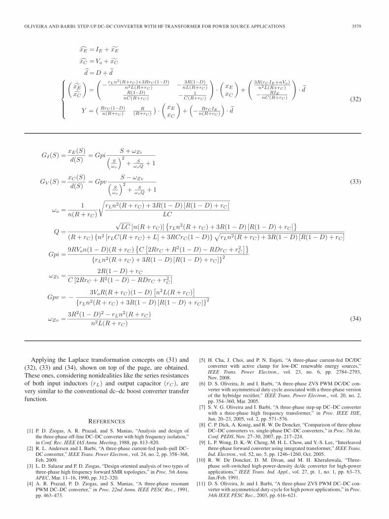
OLIVEIRA AND BARBI: STEP-UP DC–DC CONVERTER WITH HF TRANSFORMER FOR POWER SOURCE APPLICATIONS 3579
xE = IE + xE
xC =Vo + xC
d =D + d⎧⎪⎪⎪⎪⎨⎪⎪⎪⎪⎩
( ˙xE˙xC
)=
(− rLn2(R+rC)+3RrC(1−D)
n2L(R+rC) − 3R(1−D)nL(R+rC)
R(1−D)nC(R+rC) − 1
C(R+rC)
)·(
xE
xC
)+
(3R(rCIE+nVo)
n2L(R+rC)
− RIE
nC(R+rC)
)· d
Y =( RrC(1−D)
n(R+rC)R
(R+rC)
)·(
xE
xC
)+
(− RrCIE
n(R+rC)
)· d
(32)
GI(S) =xE(S)d(S)
= GpiS + ωZi(
Sωo
)2
+ SωoQ + 1
GV (S) =xC(S)d(S)
= GpvS − ωZv(
Sωo
)2
+ SωoQ + 1
(33)
ωo =1
n(R + rC)
√rLn2(R + rC) + 3R(1 − D) [R(1 − D) + rC ]
LC
Q =
√LC [n(R + rC)]
{rLn2(R + rC) + 3R(1 − D) [R(1 − D) + rC ]
}(R + rC) {n2 [rLC(R + rC) + L] + 3RCrC(1 − D)}
√rLn2(R + rC) + 3R(1 − D) [R(1 − D) + rC ]
Gpi =9RVon(1 − D)(R + rC)
{C
[2RrC + R2(1 − D) − RDrC + r2
C
]}{rLn2(R + rC) + 3R(1 − D) [R(1 − D) + rC ]}2
ωZi =2R(1 − D) + rC
C [2RrC + R2(1 − D) − RDrC + r2C ]
Gpv = −3VoR(R + rC)(1 − D)
[n2L(R + rC)
]{rLn2(R + rC) + 3R(1 − D) [R(1 − D) + rC ]}2
ωZv =3R2(1 − D)2 − rLn2(R + rC)
n2L(R + rC)(34)
Applying the Laplace transformation concepts on (31) and(32), (33) and (34), shown on top of the page, are obtained.These ones, considering nonidealities like the series resistancesof both input inductors (rL) and output capacitor (rC), arevery similar to the conventional dc–dc boost converter transferfunction.
REFERENCES
[1] P. D. Ziogas, A. R. Prazad, and S. Manias, “Analysis and design ofthe three-phase off-line DC–DC converter with high frequency isolation,”in Conf. Rec. IEEE IAS Annu. Meeting, 1988, pp. 813–820.
[2] R. L. Andersen and I. Barbi, “A three-phase current-fed push–pull DC–DC converter,” IEEE Trans. Power Electron., vol. 24, no. 2, pp. 358–368,Feb. 2009.
[3] L. D. Salazar and P. D. Ziogas, “Design oriented analysis of two types ofthree-phase high frequency forward SMR topologies,” in Proc. 5th Annu.APEC, Mar. 11–16, 1990, pp. 312–320.
[4] A. R. Prazad, P. D. Ziogas, and S. Manias, “A three-phase resonantPWM DC–DC converter,” in Proc. 22nd Annu. IEEE PESC Rec., 1991,pp. 463–473.
[5] H. Cha, J. Choi, and P. N. Enjeti, “A three-phase current-fed DC/DCconverter with active clamp for low-DC renewable energy sources,”IEEE Trans. Power Electron., vol. 23, no. 6, pp. 2784–2793,Nov. 2008.
[6] D. S. Oliveira, Jr. and I. Barbi, “A three-phase ZVS PWM DC/DC con-verter with asymmetrical duty cycle associated with a three-phase versionof the hybridge rectifier,” IEEE Trans. Power Electron., vol. 20, no. 2,pp. 354–360, Mar. 2005.
[7] S. V. G. Oliveira and I. Barbi, “A three-phase step-up DC–DC converterwith a three-phase high frequency transformer,” in Proc. IEEE ISIE,Jun. 20–23, 2005, vol. 2, pp. 571–576.
[8] C. P. Dick, A. Konig, and R. W. De Doncker, “Comparison of three-phaseDC–DC converters vs. single-phase DC–DC converters,” in Proc. 7th Int.Conf. PEDS, Nov. 27–30, 2007, pp. 217–224.
[9] L. P. Wong, D. K.-W. Cheng, M. H. L. Chow, and Y.-S. Lee, “Interleavedthree-phase forward converter using integrated transformer,” IEEE Trans.Ind. Electron., vol. 52, no. 5, pp. 1246–1260, Oct. 2005.
[10] R. W. De Doncker, D. M. Divan, and M. H. Kheraluwala, “Three-phase soft-switched high-power-density dc/dc converter for high-powerapplications,” IEEE Trans. Ind. Appl., vol. 27, pt. 1, no. 1, pp. 63–73,Jan./Feb. 1991.
[11] D. S. Oliveira, Jr. and I. Barbi, “A three-phase ZVS PWM DC–DC con-verter with asymmetrical duty-cycle for high power applications,” in Proc.34th IEEE PESC Rec., 2003, pp. 616–621.

3580 IEEE TRANSACTIONS ON INDUSTRIAL ELECTRONICS, VOL. 58, NO. 8, AUGUST 2011
[12] A. K. S. Bhat and L. Zeng, “Analysis and design of three-phase LCC-typeresonant converter,” in Proc. IEEE PESC Rec., 1996, pp. 252–258.
[13] P. Thounthong, B. Davat, S. Rael, and P. Sethakul, “Fuel cell high-power applications,” IEEE Ind. Electron. Mag., vol. 3, no. 1, pp. 32–46,Mar. 2009.
[14] S.-S. Lee, S.-W. Rhee, and G.-W. Moon, “Coupled inductor incorporatedboost half-bridge converter with wide ZVS operation range,” IEEE Trans.Ind. Electron., vol. 56, no. 7, pp. 2505–2512, Jul. 2009.
[15] S. V. Araújo, R. P. T. Bascopé, and G. V. T. Bascopé, “Highly efficienthigh step-up converter for fuel-cell power processing based on three-statecommutation cell,” IEEE Trans. Ind. Electron., vol. 57, no. 6, pp. 1987–1997, Jun. 2010.
[16] C. Pan and C. Lai, “A high efficiency high step-up converter with lowswitch voltage stress for fuel cell system applications,” IEEE Trans. Ind.Electron., vol. 57, no. 6, pp. 1998–2006, Jun. 2010.
[17] C.-S. Leu and M.-H. Li, “A novel current-fed boost converter with ripplereduction for high-voltage conversion applications,” IEEE Trans. Ind.Electron., vol. 57, no. 6, pp. 2018–2023, Jun. 2010.
[18] M. Nymand and M. A. E. Andersen, “High-efficiency isolated boost dc–dcconverter for high-power low-voltage fuel-cell applications,” IEEE Trans.Ind. Electron., vol. 57, no. 2, pp. 505–514, Feb. 2010.
[19] S.-K. Changchien, T.-J. Liang, J.-F. Chen, and L.-S. Yang, “Novel highstep-up dc–dc converter for fuel cell energy conversion system,” IEEETrans. Ind. Electron., vol. 57, no. 6, pp. 2007–2017, Jun. 2010.
[20] M. Mohr, W. T. Franke, B. Wittig, and F. W. Fuchs, “Converter systemsfor fuel cells in the medium power range: A comparative study,” IEEETrans. Ind. Electron., vol. 57, no. 6, pp. 2024–2032, Jun. 2010.
[21] G. Franceschini, E. Lorenzani, M. Cavatorta, and A. Bellini, “3boost:A high-power three-phase step-up full-bridge converter for automotiveapplications,” IEEE Trans. Ind. Electron., vol. 55, no. 1, pp. 173–183,Jan. 2008.
[22] R. W. Erickson and D. Maksimovi, Fundamentals of Power Electronics,2nd ed. New York: Kluwer, 2001, ch. 2.
[23] M. K. Kazimierczuk, Pulse-Width Modulated DC–DC Converters, 1st ed.New York: Wiley, 2008, ch. 3.
[24] S. V. G. Oliveira, C. E. Marcussi, and I. Barbi, “An average current-mode controlled three-phase step-up DC–DC converter with a three-phasehigh frequency transformer,” in Proc. IEEE 36th PESC, Jun. 16, 2005,pp. 2623–2629.
[25] F. J. Nome and I. Barbi, “A ZVS clamping mode current-fed push pullDC–DC converter,” in Proc. IEEE ISIE, Jul. 1998, pp. 617–621.
Sérgio Vidal Garcia Oliveira (S’00–M’05) wasborn in Lages, Brazil, in 1974. He received the B.S.degree in electrical engineering from UniversidadeRegional de Blumenau–FURB, Blumenau, Brazil, in1999 and the M.Sc. and Ph.D. degrees in electri-cal engineering from the Universidade Federal deSanta Catarina, Florianopolis, Brazil, in 2001 and2006, respectively.
Since 2005, he has been a Lecturer on powerelectronics and electric drives with the UniversidadeRegional de Blumenau–FURB. His research topics
of interests are ac–ac and dc–dc power converters, adjustable speed drives, dis-tributed generation systems, and converters applied to hybrid vehicle electronicsystems and to embedded systems.
Dr. Oliveira is a member of the Brazilian Power Electronics Society(SOBRAEP).
Ivo Barbi (M’78–SM’90–F’11) was born in Gaspar,Brazil, in 1949. He received the B.S. and M.S. de-grees in electrical engineering from the UniversidadeFederal de Santa Catarina (UFSC), Florianopolis,Brazil, in 1973 and 1976, respectively, and theDr.Ing. degree from the Institut National Polytech-nique de Toulouse, Toulouse, France, in 1979.
He is the Founder of the Power Electronics Insti-tute, UFSC, where he is currently a Professor and theLeader of the Power Electronics Program.
Dr. Barbi has served on the IEEE Industrial Elec-tronics Society as an Associate Editor of the IEEE TRANSACTIONS ON
INDUSTRIAL ELECTRONICS in the power converter area. He is the Founderof the Brazilian Power Electronics Society.


