A Study of Plasma Etching for Use on Active Metals Keane T ...
63
A Study of Plasma Etching for Use on Active Metals by Keane T. Nishimoto S.B. Mechanical Engineering Massachusetts Institute of Technology, 2003 Submitted to the Department of Mechanical Engineering in Partial Fulfillment of the Requirements for the Degree of Master of Science in Mechanical Engineering at the Massachusetts Institute of Technology September 2005 Copyright 2005 Massachusetts Institute of Technology. All rights reserved Signature of Author ................................................. Department of Mechanical Engineering August 16, 2005 Certified by .......... Jung-Hoon Chun Professor, Mechanical Engineering Thesis Supervisor A ccepted by ............................................................. Lallit Anand Chairman, Departmental Committee on Graduate Studies Department of Mechanical Engineering MASSjACHUSETTS INS E OF TECHNOLOGY NOV 0 7 2005 LIBRARIES 1 BARKER
Transcript of A Study of Plasma Etching for Use on Active Metals Keane T ...
A Study of Plasma Etching for Use on Active Metals
by
Keane T. NishimotoS.B. Mechanical Engineering
Massachusetts Institute of Technology, 2003
Submitted to the Department of Mechanical Engineering in Partial Fulfillment of theRequirements for the Degree of
Master of Science in Mechanical Engineeringat the
Massachusetts Institute of Technology
September 2005
Copyright 2005 Massachusetts Institute of Technology. All rights reserved
Signature of Author .................................................Department of Mechanical Engineering
August 16, 2005
Certified by ..........Jung-Hoon Chun
Professor, Mechanical EngineeringThesis Supervisor
A ccepted by .............................................................Lallit Anand
Chairman, Departmental Committee on Graduate Studies
Department of Mechanical EngineeringMASSjACHUSETTS INS EOF TECHNOLOGY
NOV 0 7 2005
LIBRARIES1
BARKER

A Study of Plasma Etching for Use on Active Metals
by
Keane T. Nishimoto
Submitted to the Department of Mechanical Engineeringon August 16, 2005 in Partial Fulfillment of the
Requirements for the Degree ofMaster of Science in Mechanical Engineering
ABSTRACT
Active metals can be used as a getter pump, removing impurities in ultra-purehigh vacuum environments. To relieve the difficulties involved with the transportation,storage and handling of these metals, a process is being developed to create a protectivecoating by removing the active metal component from the surface of a mixture of theactive metal and a stable element via immersion in a wet chemical bath.
It is the purpose of this thesis to investigate the utility of a plasma etching processin the removal of the active metal. A decision tree for the selection of a suitable etchantgas was developed and experiments were conducted to validate the process.
Magnesium coated glass slides were etched with chlorine, fluorine, andfluorocarbon gasses alone and in the presence of argon to determine which chemistrywould etch the fastest. Magnesium was chosen because it was the easiest to handleamong the active metals. It was determined that chlorine gas with argon provided thehighest etch rate. Next, a set of factorial experiments were conducted to determine thesensitivity of the etch process to changing radio frequency power input, chamberpressure, and the ratio of chlorine to argon. Factor levels were arranged in an orthogonalarray and the main effects of each parameter were estimated using analysis of means. Itwas found that the etch rate increases strongly with increasing power and decreasingamounts of chlorine. Dependence on pressure was less pronounced. These resultsindicate that the etching mechanism is dependent on physical sputtering. Etch rates of upto 30 nm/min were achieved at 350 W power, 20 mTorr chamber pressure, and a10%/90% chlorine to argon ratio.
In conclusion, although the etch rate is not currently high enough for practicaluse, the steps in the decision tree were validated by the first set of experiments while thesecond set was able to characterize the basic mechanism of the etch process.
Thesis Supervisor: Jung-Hoon ChunTitle: Professor, Mechanical Engineering
2
Acknowledgements
First of all, I would like to thank Professor Jung-Hoon Chun for giving me the
chance to do this research and for the guidance and advice along the way. You really
helped turn this into a personal learning experience as well as an academic one.
Thank you to Kurt Broderick for all your help and patience in the fab. I really
don't think that I would have gotten anywhere on this project if it wasn't for your
expertise and dedication to helping all the users of the EML. You were an invaluable
source of knowledge on practical plasma etching, and the sometimes quirky workings of
the Plasmatherm.
Thank you to Tim McClure for aiding me on the profilometer and making the lab
so accessible to everyone. It was always a nice break to come down to the CMSE and
hear some of your stories.
Thank you to Dr. Nilanjan Chatterjee and Dr. Anthony Garratt-Reed for all their
help and prompt responses to my questions on SEMs, microprobes, x-rays, and more.
Finally, a big, big thanks to my parents and sister, Angie. You guys always had a
way of telling me what I needed to hear to keep me on track. I know as a fact that none
of this would have gotten done without your love and support.
3

Table of Contents
A BSTRA CT ............................................................ 2
ACKNOWLEDGEMENTS .............................................. 3
CHAPTER 1 Introduction .............................................. 51.1 Getters and active metals ....................................... 51.2 Current active metal packaging and storage technology ................ 71.3 Proposed active metal storage method .............................. 9
CHAPTER 2 Process development ....................................... 122.1 Plasma etching .............................................. 122.2 Decision tree for etchant selection ............................... 17
CHAPTER 3 Experimentation .......................................... 233.1 Samples and apparatus ........................................ 233.2 Selection of plasma chemistry .................................. 26
3.2.1 Procedure ............................................ 263.2.2 Results ............................................ 273.2.3 Discussion .......................................... 27
3.3 Process characterization ....................................... 283.3.1 Design of experiments ................................. 283.3.2 Procedure .......................................... 293.3.3 Results ............................................ 323.3.4 Discussion .......................................... 41
CHAPTER 4 Conclusions .............................................. 454.1 Evaluation of etching results ................................... 454.2 Recommendations for future work ............................... 45
APPENDIX A Experimental data ........................................ 47
APPENDIX B Design of experiments ..................................... 59
BIBLIOGRAPHY ...................................................... 62
4

1 Introduction
1.1 Getters and active metals
Most metallic elements are prone to some degree of chemical interaction with the
environment that results in corrosion or other chemical reaction. Some metals exhibit
relatively high sensitivity to exposure to the ordinary atmosphere, corroding quickly or
reacting violently when in contact with air. These active metals include the alkali metals
(Li, Na, K, Rb, Cs), the alkali earth metals (Mg, Ca, Sr, Ba, Ra), and others including La,
Pr, Er, Eu, Yb, U, Pu, and Tl.
One of the main uses of active metals is as gas capture pumps, or getters. The
getter takes gasses out of the environment through adsorption, absorption, or chemical
compound formation. Adsorption is the deposition of gaseous elements as a solid or
liquid on the surface of the getter material. This process is slightly different from
absorption, which is the diffusion of gasses or adsorbed material into the bulk of the
getter material. These processes often take place simultaneously and are difficult to
differentiate. The use of getters dates back as far as 1894 when red phosphorus was
painted onto the inside of a carbon filament lamp to precipitate residual water vapor left
after mechanical pumping and speed up the process of exhausting the bulb and achieving
a high vacuum [Stout, Howell]. Getter technology progressed to mainstream use in the
1950s when emerging work in the semiconductor industry, space science, materials
research, and particle physics required the contaminant free environment that getters help
to create. Getter pumps are currently involved in ultra-high vacuum applications ranging
from aerospace technology to materials development.
The two main classifications of capture pumps are evaporable and non-
evaporable. In an evaporable getter pump, an active metal is sublimated and deposited on
the walls of the pump enclosure. Evaporation of the metal can be activated by resistive
or radiative heating, or by ion bombardment and physical sputtering. Evaporable getter
metals include calcium, barium, titanium, thorium, molybdenum, and zirconium
[Hucknall 99].
5

A simple evaporable getter pump is schematically shown in Figure 1.1. The
diagram shows that an evaporable getter pump can be as simple as a stainless steel body
containing the evaporation source such as a titanium filament, and sometimes a screen
collector for the evaporated material to deposit on where the gettering will take place. If
there is no screen collector, evaporated metal is deposited onto the walls of the pump
body, which then serve as the gettering surface.
Mounting flangeattached to system Vacuum gauge
Evaporable metal filament port
Filament holder
------------ ------------------------------------------ port
Pumping surface
Figure 1.1: A simple evaporable getter pump.
Non-evaporable getters (NEGs) adsorb gas on the surface and rapidly diffuse it
into the bulk of the material. Because they do not need to be evaporated, NEG materials
can be reactive at room temperature. However, oxides and carbides formed on the
surface can pacify the getter and slow sorption of gasses. To counter this pacification,
the material is heated to speed up the diffusion of oxygen and carbon into the bulk.
Common NEG metals include tantalum, titanium, or zirconium, as well as alloys
such as zirconium-aluminum or zirconium-vanadium-iron.
In general, evaporable getters are preferable to NEGs when there is enough
surface area for the evaporated material to deposit on. Examples of cases where use of an
NEG would be advantageous include systems where there is not enough surface area or
6

volume to support evaporable getter use due to space limitations of the system, the
possibility of high vapor pressure getter materials migrating into other sections of the
system, and the chance of further gas-phase reactions with the evaporated material
leading to the formation of unwanted products [Ferrario 364].
1.2 Current active metal packaging and storage technology
Titanium proves to be one of the most practical and effective materials in
evaporative getter pumps [Welch]. Titanium is much easier to handle and store than
many of the other active metals used in gettering applications. Metals with relatively
high reactivity, such as the alkali and alkali earth metals, require special considerations to
prevent contamination by contact with the environment and, in some cases, dangerously
violent chemical reactions.
There are two general methods for protecting these active metals from the
environment. The metal can either be sealed within a protective coating or mixed with
other substances to reduce its reactivity.
Sealing active metals is made difficult by the fact that they are highly reactive to
many different materials. This property rules out many developed methods of applying a
protective coating such as vapor or sputter deposition, spraying, plating, oxidation or
nitriding. At present, active metals must be stored in hermetically sealed shells, like
metal containers or glass ampoules under an inert atmosphere. Metal containers are
convenient and reliable for the storage and transportation of active metals due to their
durability and high isolation of the metal from the environment. However, because
special tools are required to open the casing or break the shell, this method makes it
difficult to extract fine dosages at the usage stage. Similarly, extraction of a precise
amount of active metal from a glass ampoule proves difficult.
The other method of protecting an active metal, mixing it with other substances to
make it less sensitive to exposure to the environment, makes it easier to control the
amount of metal being released in the usage stage. This method, however, suffers from
drawbacks related to the production, storage and use of the metal mixtures. Three
proposed methods are listed below along with their drawbacks.
7

One method of releasing vapors of an active metal A requires starting with an
inorganic compound or intermetallic compound AX, which is a stable form of active
metal A [Ferrario]. Compounds such as inorganic chromates or BaAl4 could serve as the
AX material. Exposing the compound AX to a reducing agent Me and heat releases Avap,
the vapor of A as shown as Equation 1.1,
AX + Me heat > MeX+Aap (1.1)
Some drawbacks to this type of reaction are its exothermic nature and the carcinogenicity
of chrome compounds.
Thermal decomposition of an intermetallic compound AB is another proposed
method of reducing active metal reactivity while allowing control over its release. This
mechanism is shown as Equation 1.2,
AB heat > Ava + B (1.2)
where B is the component that the active metal is mixed with. The major drawback to
this approach is that AB remains very active, retaining the difficulties in storage and
handling.
The third proposed method to combine active metals with other substances
involves organic synthesis reactions of the general form shown as Equations 1.3 and 1.4,
AY+R >AR+Y (1.3)
R A'solvent > AR (1.4)
where AY is a compound of an active metal A with an substance Y, R is an organic
substance, and the solvent can be a solution of liquid ammonia or tetrahydrofuran type.
The main drawbacks of organic synthesis are the use of flammable reagents and the
difficulty involved with separating the products of the reaction from the other dissolved
material.
8

1.3 Proposed active metal storage method
A new method was conceived and patented for the protection of active metals
during the storage and transportation phases while still allowing for the controllable
release of the metal during use [Konstantin]. The process, shown in Figure 1.2, involves
Liquid L
t t t t t t t I t I tb0000000000o0o
M ixtr
Metal A
(a)
Liquid L
U U(b
ixure A
(b)
Liquid L
Mixture AB//////// /
Islands of B metalforming
Continuous B metal
film
(c)
Figure 1.2: Progress of the Konstantin surface passification process.
creating a mixture AB of the active metal A and a stable element or alloy B. The surface
of the solidified mixture is then exposed to a liquid L that dissolves the active metal, but
does not react with the stable B material as shown in Figure 1.2a. As particles of metal A
9
are removed from the surface, small islands of pure material B begin to form as shown in
Figure 1.2b. The process is to be conducted at a temperature higher than the melting
point of material B, but lower than the melting point of metal A so that, eventually, the
molten B material fills the voids left by the departing A metal to leave a continuous,
protective coating of the stable material B as shown in Figure 1.2c.
Activation of the sealed particles is achieved by heating to above the melting
point of material B. This process will allow the protective coating to become a semi-
permeable membrane that allows atoms of the active metal A to pass through the
protective layer. Depending on the composition of the core mixture AB, the activation
process can either result in metal A migrating to the outer surface and evaporating, or it
can lead to the creation of a mixture of A and B on the surface which exhibits greater
chemical activity than pure metal A. The former is like metal vapor sources or
evaporable getters while the latter may be used as the chemisorbant in vacuum
applications that exceeds the performance of current non-evaporable getters due to its
ability to become activated at room temperature.
The Konstantin surface pacification process requires a judicious choice of both
the AB compound and the liquid L. The ongoing development of the process involves
analyzing different combinations of active metals and protective layer metals and pairing
them with appropriate liquids that will dissolve the A metal while exhibiting low or no
reactivity to the stable B metal and the mixture AB. Selection of usable components is
complicated by the fact that the B metal must melt at a temperature lower than the boiling
temperature of liquid L for it to form a continuous protective layer.
Gas and plasma phase processes can be conducted under very low pressures
resulting in longer mean free paths of gas phase species. It is therefore possible that such
a process may be able to increase the purity of the pacifying layer by decreasing the
frequency of contaminants impacting and depositing on the etched surface. Plasma
etching processes provide an appealing avenue due to their high etch rate capabilities.
However, plasma etching technology has mainly been applied to semiconductor and
micro-electro-mechanical system (MEMS) applications. The effect of the limited breadth
10

of use is that plasma etching processes have only been developed for materials used in
semiconductors or MEMS.
It is the purpose of this research to create a general set of guidelines for the
development of a process for the plasma etching of active metals. Criteria for selection
of the etching chemistry, as well as alternative dry etching processes will be presented.
That section will be followed by a description of the two sets of experiments that were
conducted. The purpose of the first set was to validate the chemistry selection process,
while the second set characterizes the process' sensitivity to changing parameters. The
procedure and results of the experiments will be presented with comments and discussion
of the data. Finally, recommendations will be made for future work on the topic.
11
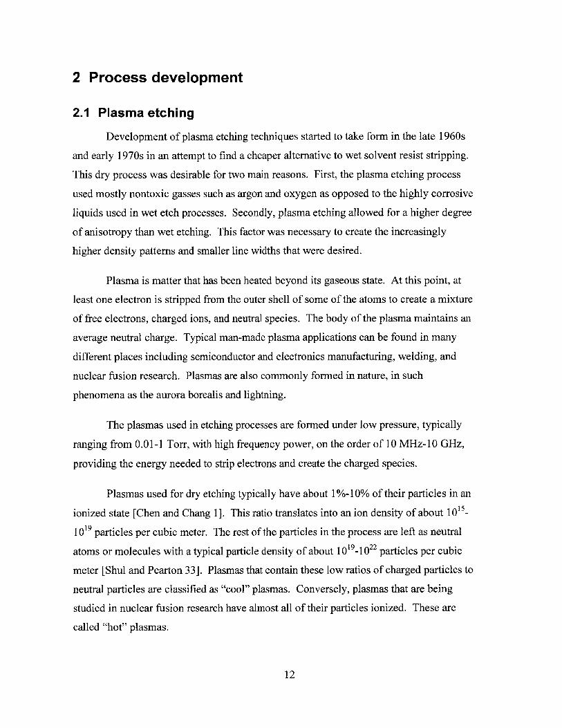
2 Process development
2.1 Plasma etching
Development of plasma etching techniques started to take form in the late 1960s
and early 1970s in an attempt to find a cheaper alternative to wet solvent resist stripping.
This dry process was desirable for two main reasons. First, the plasma etching process
used mostly nontoxic gasses such as argon and oxygen as opposed to the highly corrosive
liquids used in wet etch processes. Secondly, plasma etching allowed for a higher degree
of anisotropy than wet etching. This factor was necessary to create the increasingly
higher density patterns and smaller line widths that were desired.
Plasma is matter that has been heated beyond its gaseous state. At this point, at
least one electron is stripped from the outer shell of some of the atoms to create a mixture
of free electrons, charged ions, and neutral species. The body of the plasma maintains an
average neutral charge. Typical man-made plasma applications can be found in many
different places including semiconductor and electronics manufacturing, welding, and
nuclear fusion research. Plasmas are also commonly formed in nature, in such
phenomena as the aurora borealis and lightning.
The plasmas used in etching processes are formed under low pressure, typically
ranging from 0.01-1 Torr, with high frequency power, on the order of 10 MHz- 10 GHz,
providing the energy needed to strip electrons and create the charged species.
Plasmas used for dry etching typically have about 1%-10% of their particles in an
ionized state [Chen and Chang 1]. This ratio translates into an ion density of about 1015-
1019 particles per cubic meter. The rest of the particles in the process are left as neutral
atoms or molecules with a typical particle density of about 1019-102 particles per cubic
meter [Shul and Pearton 33]. Plasmas that contain these low ratios of charged particles to
neutral particles are classified as "cool" plasmas. Conversely, plasmas that are being
studied in nuclear fusion research have almost all of their particles ionized. These are
called "hot" plasmas.
12
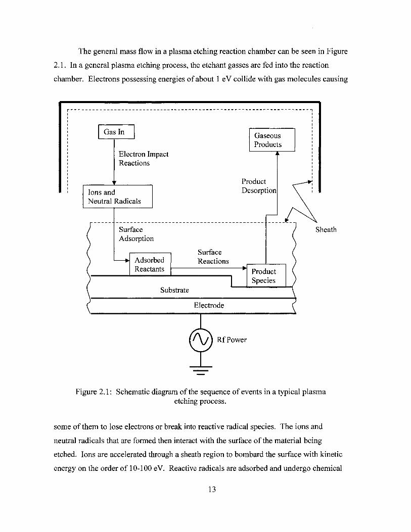
The general mass flow in a plasma etching reaction chamber can be seen in Figure
2.1. In a general plasma etching process, the etchant gasses are fed into the reaction
chamber. Electrons possessing energies of about 1 eV collide with gas molecules causing
r ------------------------------------------------------
Gas In GaseousProducts
Electron ImpactReactions
Product
Ions and DesorptionNeutral Radicals
Surface SheathAdsorption
Surface-, Adsorbed Reactions
Reactants Prdc
Substrate
Electrode
Rf Power
Figure 2.1: Schematic diagram of the sequence of events in a typical plasmaetching process.
some of them to lose electrons or break into reactive radical species. The ions and
neutral radicals that are formed then interact with the surface of the material being
etched. Ions are accelerated through a sheath region to bombard the surface with kinetic
energy on the order of 10-100 eV. Reactive radicals are adsorbed and undergo chemical
13
interactions with the surface. These surface reactions include the formation of
evaporable compounds and other product species that are then desorbed either
spontaneously or with the aid of energetic ion bombardment. Finally, the gaseous
products are recycled into more ions and neutral radicals, redeposited on the chamber
walls, or pumped out of the reaction chamber.
Plasma etching mechanisms can be separated into three general categories,
chemically based etching, ion-assisted etching, and physical sputter etching. Most
etching processes fall somewhere between these main categories. The process may rely
on chemistry to form more volatile products on the sample surface, which are then
removed physically by ion bombardment. Alternatively, the process may be mainly
chemically based, but allowed to progress at higher rates by the presence of neutral
radicals and charged species. By carrying out an etching process in between the three
main regimes of plasma etching, optimal etching parameters may be found where a
desirable rate of reaction and amount of selectivity and anisotropy are possible.
If the material being etched reacts readily enough with the molecular species
forming the plasma, pure chemical reactions can occur that carry out the etching process
without aid from ions or ionizing electrons. In this case, the reaction could take place by
simply immersing the material to be etched in the etching gas, where neutral species
combine with the surface to create volatile products that spontaneously desorb. A
schematic diagram of this process is shown in Figure 2.2. The chemical based process is
very similar to wet chemical etching. Examples of dry chemical etching are the etching
of silicon with fluorine and etching of aluminum with chlorine [Chen and Chang 167].
Among the three types of etching, pure chemical etching can achieve the greatest
level of selectivity. Since chemical reactions are the main determinant of the etch rate,
the etching gas can be chosen to etch one material over another preferentially. The main
downside of relying on chemical mechanisms in plasma etching is the loss of anisotropy.
Since one of the main benefits of plasma etching over wet etching is the anisotropic, high
aspect ratio patterns that may be formed, the highly isotropic characteristic of chemical
14

etching increases undercutting and makes it unfavorable for submicron line width
semiconductor applications.
ReactiveSpecies
Surfaceadsorption/reactions
Desorption
Volatile reactionproducts
Substrate_____1
IElectrode
Figure 2.2: Schematic diagram of a pure chemical plasma etching process.
ReactiveSpecies
Surfaceadsorption/reactions
mnbardmentace
Energetic ionbombardmentof reactionproducts
0T
Volatile reactionproducts
Substrate
Electrode
Figure 2.3: Schematic diagram of the ion-assisted plasma etching process.
Ion assisted etching makes some use of chemical reactivity between neutrals in
the plasma and the surface being etched, but unlike pure chemical etching, an inert gas
15
k
Desorption
Ion boof surf
.I
L
A
---------------------------
I F- -- -+
such as argon is added to the plasma to aid the etching process. A schematic diagram of
the ion assisted etching process is shown in Figure 2.3. Ions of the inert gas are
accelerated through a large voltage drop in the region called the sheath to bombard the
surface being etched. It is believed that the ionized inert particles enhance the formation
of volatile product molecules. In some cases, the high energy ions facilitate the
formation of products that do not form under normal conditions. Finally, the high energy
bombardment of ions may also help facilitate the desorbtion of product species. The end
effect of these factors is an etching process that can produce higher rates than chemical or
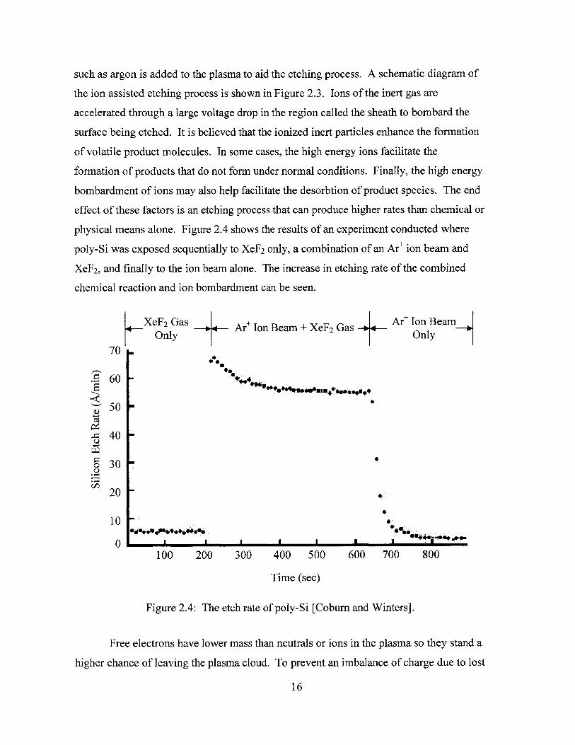
physical means alone. Figure 2.4 shows the results of an experiment conducted where
poly-Si was exposed sequentially to XeF 2 only, a combination of an Ar+ ion beam and
XeF2, and finally to the ion beam alone. The increase in etching rate of the combined
chemical reaction and ion bombardment can be seen.
XeF2 Gas + Ion Beam + XeF2 Gas -+. Ar+ Ion BeamOnly Only
70
600
50
40
30
20
10
0100 200 300 400 500 600 700 800
Time (sec)
Figure 2.4: The etch rate of poly-Si [Coburn and Winters].
Free electrons have lower mass than neutrals or ions in the plasma so they stand a
higher chance of leaving the plasma cloud. To prevent an imbalance of charge due to lost
16

electrons, a local positively charged "sheath" region is formed between the bulk plasma
and all the surfaces within the reactor. A voltage drop of up to several hundred volts may
exist across the sheath. This potential difference gives ions kinetic energy on the order of
10-100 eV and directs them perpendicular to the plane of the sheath. This directional ion
bombardment of the surface being etched allows ion assisted etching to produce isotropic
etch profiles. Some etching of sidewalls still occurs due to purely chemical interactions,
but the etch rate in the ion assisted direction will be much larger.
Purely physical plasma etching takes advantage of ion bombardment as the main
mechanism of material removal. A schematic diagram of the sputter etching process is
shown in Figure 2.5. Ions accelerated through the sheath region attain energies of up to
1 00s of eV and crash into the surface being etched, using their kinetic energy to break
bonds within the substrate being etched. Because all the ions impact traveling
perpendicular to the surface, highly anisotropic etch profiles are possible. The main
drawback of sputter etching is a lack of selectivity. The ions hit all materials with about
the same energy, so the etch yields for different substrates remains generally constant.
Sheath Ejection of sputtered) (E material
Ionbombardmentof surface " Physical sputtering
Substrate
Electrode
Figure 2.5: Schematic diagram of the physical sputter etching process.
2.2 Decision tree for etchant selection
Plasma etching processes for most materials used in the fabrication of
semiconductor devices have been experimented with and optimized for etch rate,
17

selectivity over other materials, and minimization of damage due to high-energy
bombardment and implantation. However, research on the utilization of plasma etching
on other materials for use in other sectors has generally been absent. With the current
trend towards miniaturization and micro- and nano-scale machinery, it will be of great
importance to develop patterning and manufacturing techniques to be used on a variety of
materials at that scale.
The decision tree shown in Figure 2.6 depicts a general method of developing a
plasma etch process. In the following sections, the different steps in the decision tree will
be explained in concept, followed by examples from existing etch processes.
Start
Does a volatilecompound exist?
-determine evaporability-as simple as possible
Yes
Can you make it?-spontaneous reaction
No -relative ease of formation
No
No
Is there another way toremove the compound?
-dry/wet two-step process
Yes
Yes
Does it work?-etching experiments-optimizing parameters
Yes
End
Figure 2.6: Decision tree for the selection of etchant gasses for plasma etching.
18
Material removal in a plasma etching process relies on the spontaneous desorption
of products from the surface being etched. For this reason, the existence of a volatile
target compound or family of compounds is of primary importance. This compound
should include the material being etched. In the etching of silicon, SiF 4 and SiCl 4 are the
volatile target product compounds of the etch process. Sometimes, families of etch
products are formed. In the fluorocarbon etching of Si, Si0 2 , and Si3N4 , intermediate
products of the form SiFxOy are found on the surface as products of the reaction with
chemicals in the plasma [Matsui, Tatsumi, and Sekine 1282]. Furthermore, families of
reaction products may be formed as a result of the wide variety of neutral radicals and
ions that may be present in the plasma cloud itself. For example, in plasma formed from
C2F6 gas, as many as 5 different species were detected using mass spectrometry. In
plasmas based on larger molecules, such as C5F8 , over 20 different species were detected
in various concentrations [Imai, Motomura, and Tachibana 1484].
The volatility of the target product compound would most accurately be
determined by looking at its vapor pressure at the etching conditions. However, this
information is not generally measured or recorded, and is therefore very difficult to find.
Instead of the vapor pressure, a material's melting temperature can be used as an
indicator of how easily it will be to vaporize. Figure 2.7 shows the results of etch rate
measurements of various metals [Williams, et. al] as a function of the melting point of the
reaction product of the metal with fluorine gas. The curve in Figure 2.7 is a best fit
power law curve. The metals were etched in two different fluorine chemistries, SF 6 and
CF4, in a Surface Technology Systems 320 parallel plate RIE tool under 1 00-W power at
13.56 MHz with a process pressure of 20 mTorr. Although the relationship is not perfect,
a general correlation between melting point temperature of the product and resulting etch
rate can be seen. Using this trend, it is possible to determine which family of etch gasses
will provide the highest etch rate for a specific material.
19

160
140
120
C100-
T 80
60-
40-
20-
00 200 400 600 800 1000 1200 1400 1600
Melting Point (C)
Figure 2.7: Effects of the melting point of various fluoride metal compounds onetch rate.
Once a target product compound has been chosen, it must be determined whether
or not the corresponding etch gas will be able to form the desired compound. That is, the
reaction between the surface material and the etch gas to form the evaporable product
compound must be thermodynamically favorable. If the forward, product-forming,
reaction is not naturally favored, there will be very little chemical enhancement of the
etch rate and physical sputtering mechanisms will determine the overall etch rate. In
such a case, higher energy particles will be necessary to increase etch rate, the use of
which may also lead to the undesirable consequence of damage electrical components on
the sample, as well as a loss of selectivity.
The direction that a reaction naturally progresses in can be determined by
calculating the change in Gibbs free energy,
AG = AH - TAS (2.1)
20

where AG is the change in Gibbs free energy, AH is the change in enthalpy, T is the
temperature, and AS is the change in entropy for the reaction. Equation 2.1 assumes that
the reaction is taking place at constant temperature and pressure.
A negative value of AG for the reaction indicates that it is thermodynamically
favorable and will naturally proceed to form products. If the reaction that has been
chosen to create the target product has a positive AG, the reaction will prefer to remain as
reactants instead of forming products and etching rate may be low.
In the case that there is no thermodynamically favorable reaction to create a
specific volatile product, experiments may be conducted to test the actual nature of the
reaction within the etching environment. Because plasma etching takes place under very
low pressure in the presence of very high energy particles, some reactions that are not
predicted to be carried out under normal conditions are able to proceed.
In some cases, volatile compounds of a material cannot be found. Such is the
case with many of the alkali and alkali earth metals which form mostly high melting
temperature salts when exposed to the halogens. Other metals, such as silver and copper,
also form nonvolatile, high melting temperature compounds when exposed to halogens.
If etching of such a material is desired, alternate means of material removal must be
found. One such method that has been developed utilizes a combination of dry and wet
etching processes. In general, a plasma or dry chemical etch is used to create reaction
products on the surface of the sample. A solvent bath is then used to selectively remove
the product compound from the surface.
By applying a plasma etch followed by a wet chemical etch, material removal
rates of up to 200 nm/min have been reported [Nguyen, et. al]. The documented process
exposed silver films to plasmas composed of CF 4 and CF4 mixed with 02 followed by
soaking of the sample in Microstrip-3001 solvent which removed the photoresist mask as
well as reacted silver-fluorine compounds.
Other groups have developed two step etching processes for silver as well as
copper. Higher etch rates coupled with deeper diffusion of reactive neutral particles into
21

the film being etched have been achieved. Under a Cl2 inductively coupled plasma
raising the substrate temperature was found to allow etch rates as high as 1000 nm/min
when the substrate was heated to 200C [Park, et. al 287]. Furthermore, etch rates of
about 200 nm/min were achieved for the two step etching of copper in a C12 plasma
followed by a dilute HCl bath [Lee and Kuo].
22

3 Experimentation
Experiments were conducted to test the utility of the decision tree presented in
Section 2.2. The first set of experiments exposed samples coated with magnesium metal
to a variety of etchant chemistries to determine which would work best. The etch depth
for each trial and the most readily formed compounds as a result of exposing magnesium
to each gas were recorded to test the validity of using melting point as an indicator of
relative evaporability. From the results, the most suitable etch chemistry was chosen to
be used in the rest of the experiments.
A second set of experiments used an organized factorial experiment to
characterize the etch process with respect to source power, background pressure, and the
ratio of the two etchant gasses. An array of nine experiments was conducted and the
relative effects of each process parameter were estimated based on the results.
This section will start with an outline of the samples and equipment used in the
experiments followed by the procedure, results, and discussion of the two sets of
experiments that were performed.
3.1 Samples and apparatus
The samples being etched during the experimental process were composed of a
glass substrate coated with 0.5 ptm of pure magnesium. The glass substrates were created
by cutting 25-mm x 75-mm glass microscope slides into approximately 12-mm x 12-mm
pieces. The slides were scored with a normal, handheld glass cutter wheel.
Magnesium was selected as the material to be etched because it is the most easily
handled member of the alkali or alkali earth metal groups. The other elements in these
groups undergo more vigorous reactions when they come in contact with the air.
Magnesium may also be immersed in water without causing a violent reaction. This
feature was viewed as a positive as it would aid any investigation into a two-step process
involving removal of a water-soluble salt as described in Section 2.2.
23
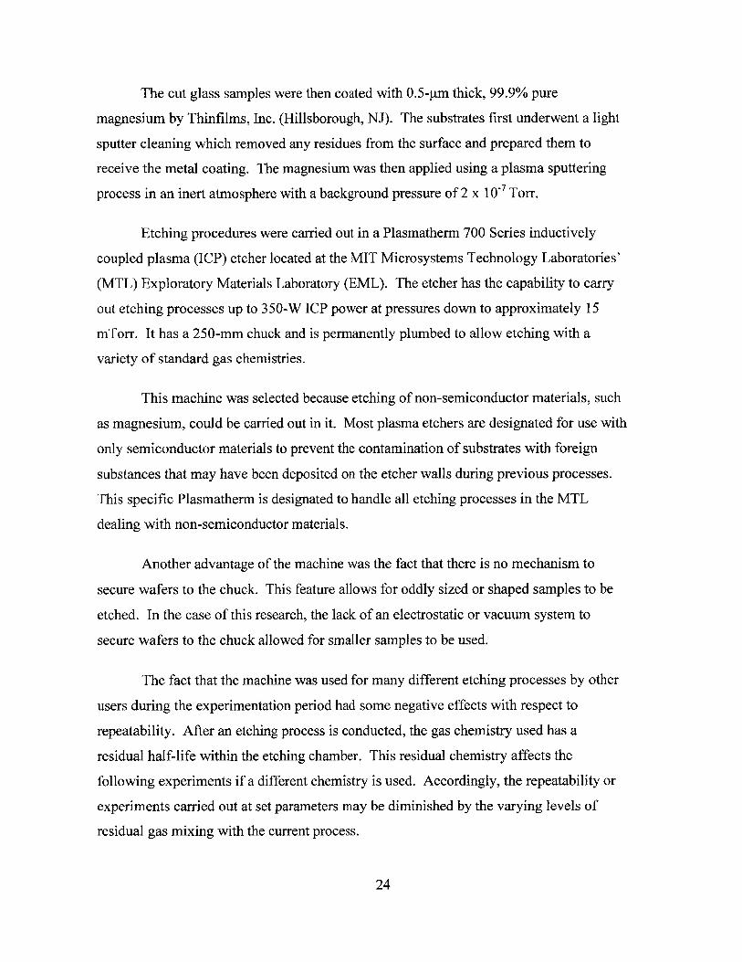
The cut glass samples were then coated with 0.5-ptm thick, 99.9% pure
magnesium by Thinfilms, Inc. (Hillsborough, NJ). The substrates first underwent a light
sputter cleaning which removed any residues from the surface and prepared them to
receive the metal coating. The magnesium was then applied using a plasma sputtering
process in an inert atmosphere with a background pressure of 2 x 10⁻⁷ Torr.
Etching procedures were carried out in a Plasmatherm 700 Series inductively
coupled plasma (ICP) etcher located at the MIT Microsystems Technology Laboratories'
(MTL) Exploratory Materials Laboratory (EML). The etcher has the capability to carry
out etching processes up to 350-W ICP power at pressures down to approximately 15
mTorr. It has a 250-mm chuck and is permanently plumbed to allow etching with a
variety of standard gas chemistries.
This machine was selected because etching of non-semiconductor materials, such
as magnesium, could be carried out in it. Most plasma etchers are designated for use with
only semiconductor materials to prevent the contamination of substrates with foreign
substances that may have been deposited on the etcher walls during previous processes.
This specific Plasmatherm is designated to handle all etching processes in the MTL
dealing with non-semiconductor materials.
Another advantage of the machine was the fact that there is no mechanism to
secure wafers to the chuck. This feature allows for oddly sized or shaped samples to be
etched. In the case of this research, the lack of an electrostatic or vacuum system to
secure wafers to the chuck allowed for smaller samples to be used.
The fact that the machine was used for many different etching processes by other
users during the experimentation period had some negative effects with respect to
repeatability. After an etching process is conducted, the gas chemistry used has a
residual half-life within the etching chamber. This residual chemistry affects the
following experiments if a different chemistry is used. Accordingly, the repeatability or
experiments carried out at set parameters may be diminished by the varying levels of
residual gas mixing with the current process.
24

A further drawback of the machine used to carry out etching experiments was the
lack of a substrate temperature control. Because the volatility of many substances is tied
closely to temperature, the ability to control the substrate temperature is desirable.
However, for the reasons mentioned above regarding the difficulty in finding facilities to
etch non-semiconductor materials, the lack of substrate temperature control was
unavoidable in this study.
Finally, the gasses available for use in etching processes was limited by the fixed
plumbing connected to the etcher. A schematic diagram of the gas distribution system is
shown in Figure 3.3. The etching gasses are paired up with each pair corresponding to
one channel. For any given etching process, one gas may be chosen on each channel.
For example, an etching process may use either HC23 or BCl 3, but not both. In the same
manner, a process may use argon or methane, chlorine or SF 6, and/or helium or oxygen.
For any process, the mass flow controller (MFC) for a channel may be closed so that
neither gas on that channel is included in the etching chemistry.
Mass FlowControllers (MFCs)
BCTl_
Ar
CH4 Toetching
Cl2 chamber
SF6
He
02
Figure 3.3: Schematic diagram of the gasetcher.
distribution system for the plasma
25

3.2 Selection of plasma chemistry
The purpose of the first set of experiments was to survey the available gas
chemistries and determine which, if any, could etch the magnesium deposited on the
samples. The results of this experiment would also be used to validate or disprove the
selection criteria presented in Section 2. Characterizing experiments would follow once
the most effective etchant was determined, so for this experiment, it was desired simply
to qualitatively observe which gas produced the best results.
3.2.1 Procedure
Of the available gasses shown in Figure 3.3, helium and oxygen were not used in
this experiment due to the low chemical reactivity of helium, and the assumed formation
of magnesium oxide upon exposure of the samples to oxygen. From the remaining
gasses, CH 4 was not examined because it was desired to try each chemistry with and
without argon sputtering, and since argon and methane are on the same channel, it was
not possible to control the proportion of each gas fed to the etching chamber. The
remaining gasses, SF 6, Cl2 , BCl 3, and the fluorocarbon HC23 (CHF 3) were used one at a
time alone and in combination with argon in the order listed in Table 3.1. For all trials,
the power was set at 300 W with a background pressure of 25 mTorr.
Table 3.1: Gas chemistries and their respective flow rates used in selection ofplasma chemistry experiments.
Chemistry Flow Rate(sccm)
SF 6 25SF 6/Ar 13/13
Cl2 25C12/Ar 13/13BCl 3 25
BCl3/Ar 13/13CHF3 25
CHF3/Ar 13/13Ar 25
Prior to etching, a piece of glass microscope cover slide measuring approximately
3mm x 3mm was placed on top of the sample to act as a mask. The area under the mask
26

would not be exposed to the plasma and would serve as a reference height to determine
how much etching had taken place.
The etched samples were examined using a Tencor P-10 surface profilometer. At
least 3 scans were taken for each sample along the cleanest masked edge. Using the
profilometer's integrated leveling algorithm, the scan data was manipulated so that the
masked area showed up as level.
3.2.2 Results
The samples that were etched with SF 6 and CHF3 showed very little activity. The
fluorocarbon chemistry with the addition of argon appeared to have removed about 30 A
of material during the 5-minute etch period.
The chlorine containing gasses, Cl2 and BCl 3, displayed greater reactivity
resulting in approximately 100-A and 50-A etch depths respectively when combined with
argon. These samples also contained a large rough area adjacent to the masked edge, as
well as a texture over the rest of the sample. For the C12 and argon etched sample, the
rough area was up to 1000 ptm wide with peaks of about 6000-8000 A. The texture over
the rest of the sample was composed of 1000-2000-A peaks spaced about 50 jim apart.
The rough area on the BCl 3 and argon etched sample was much rougher with peaks in the
12000-14000 A range. The rest of the sample was also much rougher with closely spaced
bumps of about 4000-6000 A height.
In all cases, the samples etched without argon exhibited smaller step heights and
greater roughness in the etched areas.
3.2.3 Discussion
The fact that the chlorine containing gasses showed an increased etch rate over
the fluorine compounds supports the theory presented in Section 2. It is assumed that the
reaction between magnesium and chlorine will form magnesium salts, particularly,
magnesium chloride, MgCl 2. In the presence of fluorine, magnesium, which easily shares
2 electrons from its outer shell, will most likely react to form MgF2. Although neither of
27

these compounds exhibits spontaneous volatility, it was predicted that MgC 2, with a
melting point of 714 'C compared to 1263 'C for MgF2, would be easier to etch.
The rough area adjacent to the masked area is a common etching phenomenon
known as shadowing. The relative height of the mask material, the glass slide cover in
this case, blocks gas flow and ion bombardment of areas near it. This effect slows
etching within the shadowed region as well as providing a sheltered area for gas-phase
compounds to deposit themselves.
Roughness found in other areas of the etched samples is suspected to be due to the
low volatility of the compounds formed during the process. The roughness was more
pronounced on samples that were etched without the addition of argon, supporting the
theory that they are nonvolatile reaction products or redeposited material. The addition
of argon lessened the roughness by providing a physical sputtering effect that could
energetically break off the nonevaporable compounds.
3.3 Process characterization
After determining that C12 with argon provided the best results of the available
etchant chemistries, a series of experiments was conducted to characterize the sensitivity
of the process to three controllable parameters: source power, background pressure, and
C12/Ar ratio.
3.3.1 Design of experiments
A matrix experiment was used to investigate the dependence of the etch process
on each of the three factors. The three levels of each factor are shown below in Table
3.2. The levels were limited by the capabilities of the Plasmatherm etcher. The power
Table 3.2: The factors and levels used in the sensitivity experiments.
LevelsFactor 1 2 3
A. Source power (W) 150 250 350B. Background pressure (mTorr) 15 30 45C. C12/Ar ratio (%C12/%Ar) 90/10 50/50 10/90
28

setting was limited to a 350-W maximum because the etcher could not produce higher
outputs. The pressure levels were limited on the low end because the etcher had a
difficult time keeping the plasma ignited at pressures lower than 15 mTorr. Finally, the
C12/Ar levels were set to cover the full range of the experimental region.
The settings for each experiment were selected based on the standard orthogonal
L9 Taguchi array [Phadke 44]. The settings for each experiment are shown in Table 3.3.
The specific combinations of factor levels for each experiment are chosen to preserve a
balance so that, for any pair of columns, every possible combination of levels appears
exactly once. This feature is important because it allows the effects of each of the three
factors to be determined by conducting only nine experiments, compared with the 27
experiments that it would take to run every combination of factor levels once. More on
the design of experiments can be found in Appendix B.
Table 3.3: The factor level settings for each run of the matrix experiment asadapted from the L9 Taguchi standard orthogonal array.
Factor
A. Source B. Background C. C12/Ar ratioTrial No. Power level pressure level level
1 1 1 1
2 1 2 2
3 1 3 3
4 2 1 2
5 2 2 3
6 2 3 1
7 3 1 3
8 3 2 1
9 3 3 2
3.3.2 Procedure
Since the etcher being used in these experiments is in a shared facility, the etch
chamber had to be cleaned and prepared before any experiments were run. First, an
oxygen plasma was ignited at 250 W and 45 mTorr for 15 minutes to clean the chamber
29

walls of residual compounds that may have been deposited on them during previous runs.
Next, a dummy run using a C12/Ar plasma was run for 15 minutes with no sample in the
chamber to condition the etch chamber with the atmosphere that would be used for the
characterizing experiments. A polyamide sheet was placed on the bottom electrode to
increase the repeatability of experiments by suppressing residual chemistry effects from
previous runs. The same polyamide sheet was used for all experiments.
Following the cleaning and conditioning of the chamber, the orthogonal
experiments were conducted. Trials were run in a random order in an attempt to
minimize the effects of systemic variations and processing flaws. The samples were
again masked using a small piece of microscope cover glass and were placed in the center
of the etch chamber on top of the polyamide sheet. Each trial began by pumping the
chamber below 5 mTorr followed by purging the chamber of moist air by pumping
nitrogen gas through it. The chamber would then be pumped down below 5 mTorr again
before the desired C12/Ar chemistry was pumped in for 45 seconds at the desired
proportion. During the next step, the plasma was ignited and allowed to bum at the
specified factor levels for 5 minutes. After plasma shutoff, 2 more cycles of purging and
evacuating the chamber took place before the chamber was vented to atmospheric
pressure and the etched sample was removed.
During experimentation, it was found that the etcher could not ignite the plasma at
15 mTorr. To solve this problem the plasma was lit at 45 mTorr and stepped down to 30
mTorr. The pressure was allowed to settle for approximately 20 seconds after which the
pressure setting was stepped down again to 15 mTorr. Even though the pressure was set
to 15 mTorr, the etcher was only able to reduce chamber pressure to approximately 20
mTorr.
Measurements of etch depths were again conducted on a Tencor P- 10
profilometer. The software running the profilometer adjusted the data so that the
averages of two specified sections of the line plot were level. This feature allowed the
resulting plots to be manipulated so that the portion of the scan relating to the section of
the sample under the mask appeared level. The step height was then determined by
30

comparing the average height of the section of the plot corresponding to the masked
section of the sample to the average of a small, flat section of the plot in the etched region
of the sample.
The recorded step height data was used to determine the relative contributions of
each factor. The effect of each factor level was calculated by taking the average of
results from each trial that the factor was included in. For example, if hi is the step height
measured for trial i, the effect of etching at 15mTorr can be found by calculating the
average of Runs 1, 4, and 7,
M 5 mTor= (h,+h 4 +h7 ) 3.1)
where msmTorr is the average step height achieved when the pressure was set at 15
mTorr, also known as the main effect. The effect of each level of each factor was
calculated the same way and graphed to show the main effects of each factor.
Optical images of the sample surfaces were captured using a Carl Zeiss Axioplan
optical microscope and an attached Carl Zeiss Axiocam MRc digital camera. The
microscope was operated in reflected light mode since transmission of light through the
samples would have been minimal. Images were magnified by a lOx objective lens on
the microscope before being recorded using Zeiss' Axiovision software package.
The etched areas of samples were also analyzed in a JEOL JXA-733 Superprobe
electron probe microanalyzer (EPMA). The EPMA analyzes the x-ray spectrum that is
generated by the sample in response to striking the surface with a focused electron beam.
The intensity of the x-rays was measured by energy dispersive spectrometry to get a
qualitative indication of the elements present in the etched area of the samples.
Compositional analysis of the surface deposits was complicated by the deposited
layer, which was too thin to prevent transmission of electrons through it. Electrons that
penetrated the surface deposits would reflect x-rays from the glass substrate as well as the
pure magnesium layer. These penetrating electrons rule out use of x-ray diffraction since
31
a wide "amorphous curve" would result from interference of the glass and drown out
signal peaks.
Quantitative analysis of the compounds left on the surface may have been
possible using a transmission electron microscope (TEM). To prevent interference from
layers beneath the deposited compound, it would be necessary to remove the rough
crystals from the samples without capturing the pure magnesium beneath them and apply
them to carbon tape. To get accurate results the TEM requires that the tops of the crystals
be very flat and normal to the microscope's electron beam. This level of precision could
be met by ion-beam milling the crystals.
The EPMA was selected for use because it was able to provide reasonable,
qualitative data quickly and with no sample preparation necessary.
3.3.3 Results
Below are some typical profilometer scan plots and optical microscope images of
sample surfaces after etching in several trials. These images were chosen because they
will be used as examples to explain the possible causes of roughness in the etched area in
the discussion section. Typical profilometer data and optical images of trials at all
settings can be found in Appendix A.
The profile of a sample that was etched at 150 W, 45 mTorr, and with a 10%/90%
ratio of C12 to argon is shown in Figure 3.4. The masked area proceeds up to the 200-gm
mark with typical roughness of 500-1500-A height in the etched section. A change in
slope accompanies the shift from the masked portion to the unmasked portion. This
feature appeared in almost all of the profilometer scans that were taken
32

2000
1500
E 10000-
500
-5000 100 200 300 400 500 600 700 800
Length (um)
Figure 3.4: Profilometer scan of sample etched at 150 W, 45 mTorr with10%/90% C12/Ar ratio.
Figure 3.5 is a 1 Ox optical image of a sample that was etched at 150-W source
power with a background pressure of 45 mTorr and 10%/90% C12/Ar ratio. The masked
area is the smooth region on the right. The transition at the end of the masked region is
clearly visible, as is the texture appearing in the etched portion of the sample. The dark
spots and lighter squiggles that appear in the etched portion of the sample are
unvaporized or redeposited compounds that cause the surface roughness seen in the
profilometer scans.
33

Figure 3.5: Optical image of a sample etched at 150 W, 45 mTorr, and a10%/90% C12/Ar ratio.
A line plot taken on a sample that was etched at 350 W with a background
pressure of 20 mTorr and a 90%/10% ratio of Cl2 to argon is shown in Figure 3.6.
Samples etched at this setting were very smooth with widely spaced peaks. The mask
extended to just past the 200-pm mark in the scan. Note the built up peak that formed at
the edge of the mask by the shadowing effect described earlier.
Figure 3.7 is an optical image of the surface of a sample that was etched at 350
W, 20 mTorr, and a 10%/90% ratio of Cl2 to argon. The masked portion of the sample
appears on the right side of the image. Note how sparsely present the roughness features
are on the etched portion of the sample. This feature was typical of samples etched at this
setting. Also note the light build up near the end of the mask due to shadowing effects.
34

3500
3000 -
2500 -
E 2000 -0I-
0)1; 1000-
500 -
0-
-500-0 100 200 300 400 500 600 700 800
Length (urn)
Figure 3.6: Profilometer scan of a sample etched at 350 W, 20 mTorr, and a10%/90% C12/Ar ratio.
Figure 3.7: Optical image of a sample etched at 350 W, 20 mTorr, and a10%/90% C12/Ar ratio.
35
-~
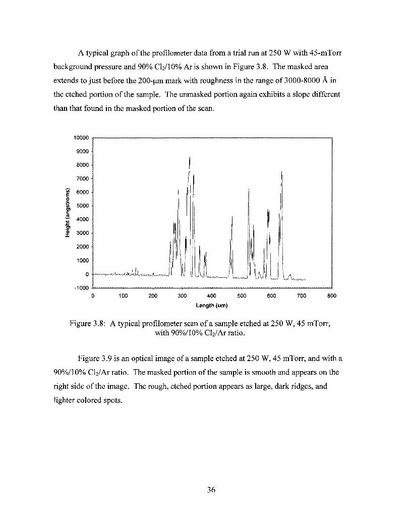
A typical graph of the profilometer data from a trial run at 250 W with 45-mTorr
background pressure and 90% C12/10% Ar is shown in Figure 3.8. The masked area
extends to just before the 200-jim mark with roughness in the range of 3000-8000 A in
the etched portion of the sample. The unmasked portion again exhibits a slope different
than that found in the masked portion of the scan.
U)E0
UOC)'U
CM
10000
9000 -
8000 -
7000 -
6000 -
5000 -
4000 -
3000 -
2000 -
1000 -
0-
-1000 -0 100 200 300 400
Length (urn)
500 600 700
Figure 3.8: A typical profilometer scan of a sample etchedwith 90%/10% C12/Ar ratio.
800
at 250 W, 45 mTorr,
Figure 3.9 is an optical image of a sample etched at 250 W, 45 mTorr, and with a
90%/10% C12/Ar ratio. The masked portion of the sample is smooth and appears on the
right side of the image. The rough, etched portion appears as large, dark ridges, and
lighter colored spots.
36

Figure 3.9: Optical image of a sample etched at 250 W, 45 mTorr, with90%/10% C12/Ar ratio.
Figure 3.10 is a scan typical of the experiments run at 250-W power and a
pressure of 20 mTorr. The chemical fraction for this run was 50% Cl2 to 50% argon.
The sample was masked until just past the 200-pm point of the scan. The scan reveals
must less roughness than the previous examples with just a couple of peaks in the 1000-
2000 A range.
Figure 3.11 is an optical image of a sample etched under the same conditions as
the one scanned in Figure 3.8. Once again, the edge of the masked area is clearly defined
with an abrupt transition into the texured, etched area. Note that the texture, although
very densely present, appears as smaller dots compared to the larger squiggles and
connected ridges shown in the etched area of the sample in Figure 3.9.
37

2500
2000-
1500-E
0)1000-
500-
0-
? T ~
0 100 200 300 400 500 600 700
Length ( urn)
Figure 3.10: Profilometer scan of sample etched at 25050%/50% C12/Ar ratio.
W, 20 mTorr, and a
Figure 3.11: Optical image of a sample etched at 250 W, 20 mTorr, and a50%/50% C12/Ar ratio
38
800-500
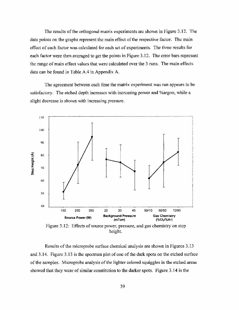
The results of the orthogonal matrix experiments are shown in Figure 3.12. The
data points on the graphs represent the main effect of the respective factor. The main
effect of each factor was calculated for each set of experiments. The three results for
each factor were then averaged to get the points in Figure 3.12. The error bars represent
the range of main effect values that were calculated over the 3 runs. The main effects
data can be found in Table A.4 in Appendix A.
The agreement between each time the matrix experiment was run appears to be
satisfactory. The etched depth increases with increasing power and %argon, while a
slight decrease is shown with increasing pressure.
110
100
90
R)
0.
0
80
70
60
50
40
150 250 350 20 30 45 90/10 50/50 10/90
Source Power (W) Background Pressure Gas Chemistry(mTorr) (%C12/%Ar)
Figure 3.12: Effects of source power, pressure, and gas chemistry on stepheight.
Results of the microprobe surface chemical analysis are shown in Figures 3.13
and 3.14. Figure 3.13 is the spectrum plot of one of the dark spots on the etched surface
of the samples. Microprobe analysis of the lighter colored squiggles in the etched areas
showed that they were of similar constitution to the darker spots. Figure 3.14 is the
39

spectrum plot of a smooth region of the etched surface. This plot is very similar to Figure
3.13 except that the chlorine peak is absent.
Si
Mg
0 2 4 86keV
Figure 3.13: Microprobe spectrum of rough etched area.
Mg
0
Si
Ca
CLK
2 4keV
6 8
Figure 3.14: Microprobe spectrum of smooth etched area.
40
Cl Ca
K

Due to the problems associated with electrons penetrating the crystals on the
surface explained in Section 3.3.2, Si, K, and Ca peaks representing the glass substrates
are present. Since the Cl peak appears in Figure 3.13 and is absent from Figure 3.14, it is
concluded that the crystals are some combination of magnesium and chlorine.
3.3.4 Discussion
The trends expressed in Figure 3.12 can be used to describe the general
mechanisms by which the magnesium was etched. The fact that the amount of material
etched increased with increasing power, decreasing pressure, and increased proportion of
argon showed that the process is dominated by a physical sputter etching mechanism.
This result was expected based on the chemical compounds that were expected to be
formed most readily during exposure of the magnesium to a chlorine atmosphere. As
mentioned earlier, the magnesium salt, MgCl 2, is not spontaneously evaporable at low
temperatures. Therefore, the etching process was expected to depend on physical
sputtering to remove the compound once it has formed on the surface.
Increasing the power being put into the system increases the amount of ionization
that takes place within the plasma. This allows a greater degree of formation of Ar+ ions
that are responsible for the physical sputtering of the surface. Each ion that impacts the
surface transfers some of its energy into the surface and has a chance to physically break
some particles free. An increase in the number of ions hitting the surface logically results
in a greater amount of material being sputtered off.
Decreasing pressure within the etching chamber increases the amount of sputter
etching by increasing the energy possessed by ions bombarding the surface being etched.
A lower pressure increases the mean free path of particles in the etching chamber. A
longer mean free path relates to a decrease in the amount of collisions between particles.
Of particular interest is the decrease in collisions between electrons and neutrals. If the
number of collisions between electrons and neutrals is decreased, more electrons are
allowed to try to escape the plasma. In an attempt to slow this escape of charged particles
from the plasma, the insulating sheath layer that forms between the plasma and the
chamber's surfaces thickens. The voltage drop across the sheath also increases. This
41
increase in voltage drop causes ions to be accelerated at a greater rate toward the surfaces
of the chamber, including the sample being etched, thereby increasing the amount of
physical sputter etching that takes place.
The sputter dominated etching mechanism is also supported by the increased etch
rate as the amount of argon was increased. A higher fraction of argon in the etching
recipe allowed a greater amount of Ar+ ions to form, resulting in more bombardment of
the surface and more sputter etching yield.
The roughness present in most of the etched specimens may be a result of
nonevaporable compounds that formed on the surface and were not sputtered off,
redeposition of compounds that were initially located in the gas phase, or, more likely, a
combination of the two.
The theory that the roughness was due to nonevaporable compounds that were not
removed from the surface is supported by Figures 3.4 and 3.6. The sample represented in
Figure 3.4 was etched with a low fraction of Cl2 and retained a rough surface while the
sample shown in Figure 3.6 was etched with the same amount of C12 , but has a very
smooth etched surface. These features can also be seen in the corresponding images,
Figure 3.5 displays a greater frequency of rough compound built up on the surface when
compared to the relatively clean surface of the sample in Figure 3.7. The higher power,
350 W versus 150 W, and low pressure, 20 mTorr to 45 mTorr, of the sample in Figure
3.7 caused a greater degree of sputter etching which was able to remove most of the
compound that remained in Figures 3.4 and 3.5.
Redeposition of gas phase compounds can be seen by comparing Figure 3.8 to
Figure 3.10. Figure 3.8 shows much more roughness as the peaks are higher and closer
together than those found in Figure 3.10. Comparing the optical image in Figure 3.9 to
the one in Figure 3.11 reveals that the bumps are also larger in size. The marks in Figure
3.9 appear as an interconnected system of ridges while those found in Figure 3.11 appear
to be small, discrete spots. Both samples were etched at the same power with similar gas
fractions. The main difference lies in the pressures at which the two samples were
etched, 20 mTorr for the sample in Figure 3.10, and 45 mTorr for the sample in Figure
42

3.8. The higher pressure may have decreased the amount of sputtering by a bit, but it
could also have caused more evaporated compounds to strike the surface with a chance of
condensing and redepositing themselves. The increased height and area of the bumps
also seems to indicate that redeposition was the cause of the roughness because both
samples would have exhibited roughness of about the same size if it was only caused by
the formation of higher volume nonevaporable compounds.
The change in slope on the profilometer scans was worrisome because it was
difficult to distinguish whether it originated from an artifact of the measurement process,
or if the slope physically existed on the surface. Since the transition was observed in
every scan, and to greatly varying degrees on different scans of the same sample, it was
determined that the slope is an artifact of the scan process. On the scale of the features
that were measured, unnoticeable rocking of the sample due to debris under the sample
during scans or a bumpy interface between the sample and the profilometer's translating
table could result in such an effect. However, because the slope change appeared in
every scan exactly at the point where the masking ends, it is unlikely that dust or a bumpy
interface was the cause. It is more likely that the feature came from a change in
electrostatic or frictional forces between the sample and the profilometer's stylus as the
tip moved from the smooth, masked area to the rough, etched area. Interactions at the
micro-scale, where masses and forces are very small, are more greatly influenced by
electrostatic, rather than inertial, forces. If the etched and masked areas built up different
amounts of static charge due to varying chemical compositions and topography, the
resulting change in electrostatic force could be responsible for the observed slope.
Another possible cause of the artifact was the light, 6-mg touch of the stylus against the
surface. As the tip translated over relatively large peaks in the etched region, it may have
lost contact for short periods of time, leading it to report false data.
Based on the EPMA data, it can reasonably be concluded that the compound
deposited on the samples was magnesium chloride, MgCl 2. Magnesium normally takes
up a 2+ charge due to relatively low first and second ionization energies of 737.7 kJ/mol
and 1450.7 kJ/mol, respectively. More electrons are not normally shared because the
third ionization energy of magnesium is much higher at 7732.7 kJ/mol. On the other
43

hand, chlorine is a halogen with a valence shell missing one electron. Chlorine is very
electronegative with a Pauling scale value of 3.16, readily accepting 1 electron to end up
at a I- charge. For these reasons, it is very unfavorable for magnesium and chlorine to
form compounds other than MgCl 2.
44

4 Conclusions
4.1 Evaluation of etching results
It was the purpose of this thesis to outline a general process to facilitate the
selection of an etchant that would work with materials that are not normally used in the
semiconductor industry, specifically active metals. The decision tree featured in Chapter
2 was tested and the data from experimentation seems to indicate that the outlined steps
can be used to select a working etchant species. Although the range of etchant
chemistries was limited to those normally used for semiconductor processes, the
principles of the decision tree were confirmed. Chlorine gas was found to be more
effective at etching the magnesium coated samples than either fluorine or fluorocarbon
chemistries. This result supports the theory that comparable suitability as an etchant can
be determined by the melting temperature of compounds formed by reaction between the
gas and surface.
The etching characterization experiments were not as successful as the etch
chemistry selection process. Within the available parameter range, the magnesium films
etched very slowly. Etch rates of up to 30 nm/minute would not be sufficient for use in a
process to pacify active metals. Furthermore, the large amount of redeposited or
unetched compounds found on the surface of the etched samples is undesirable. Active
metal getter pumps are intended for use in ultra-clean environments, where purity of the
metals is crucial. Therefore, contamination of the etched surface by etchant gas or
redeposited compounds would not be acceptable.
4.2 Recommendations for future work
This thesis has shown that plasma etching of active metals is possible. However,
it has also shown that much more must be understood before the process can be used in
the production of active metals with a pacified surface. The main problems that must be
solved at present are the low etch rate and the contamination of the etched surface by
compounds containing the etchant gas. Secondary problems such as selectivity of the
etch process over prospective stable B materials, as depicted in Figure 1.2, and further
45
characterization of the etch process must also be investigated before plasma etching of
active metals is practical. The following research topics are proposed to further develop
the work started in this thesis:
1. Find an etchant that is more effective than those normally used in the
semiconductor industry. Active metals are called active because they
react with many different substances. Arriving at a chemistry that can
achieve greater etch rates than conventional gasses would be a large
step toward applying plasma etching technology toward pacifying
active metals.
2. Run characterizing experiments in different parameter ranges. The
range of settings available in this work was limited by the capabilities
of the available etcher. Newer machines can handle higher powers and
sustain plasmas at lower pressures. They also have additional features
such as substrate temperature control. Spectroscopic analysis of the
gasses within the etch chamber, as well as those flowing out of it
would provide information about the compounds being removed from
the substrate.
3. Experiment with a plasma etch followed by immersion in a wet bath.
TEM analysis of the residual compounds on the etched surface to
determine their exact chemical composition will prove helpful in
choosing a wet bath chemistry that will dissolve the compound, but not
react with the active metal. Also, optimizing the cycle times for
etching and immersion to balance the process, along with batch
processing, could increase throughput to practical levels.
46
Appendix A
Experimental data
Raw data from the characterization experiments is presented in this appendix.
Included are graphs of typical results for each of the nine trial settings that were run for
the factorial experiment, optical images of the etched samples' surfaces, and tables listing
the measured step height for each sample, as well as the calculated values of the main
effects of each factor value.
In the following figures, the masked area typically ends just before the 200-pm
mark. Characteristic buildup of redeposited material is usually present following the
interface, with the normal roughness of the bulk of the etched area further down the scan.
E0
9000
8000
7000
6000
5000
4000
3000
2000
1000
0
-10000 100 200 300 400
Length (urn)
500 600 700 800
Figure A. 1: A typical profilometer plot of a sample etched at 150 W, 20 mTorr,and a 90%/10% C12/Ar ratio.
47
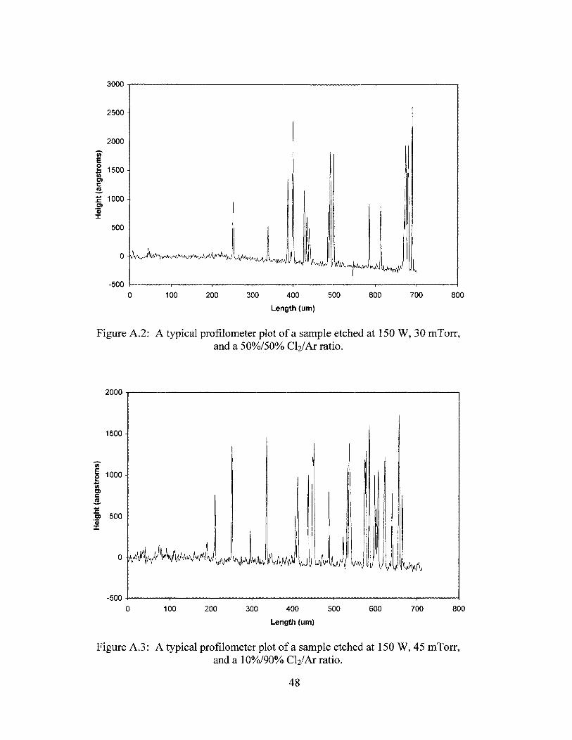
3000
2500 -
2000 -
E0. 1500 -
CM
1000 -
500-
0-
-5000 100 200 300 400 500 600 700 800
Length (urn)
Figure A.2: A typical profilometer plot of a sample etched at 150 W, 30 mTorr,and a 50%/50% C12/Ar ratio.
2000
1500 -
2 1000-00-U)
C
0)500 -Z
0
-5000 100 200 300 400 500 600 700 800
Length (urn)
Figure A.3: A typical profilometer plot of a sample etched at 150 W, 45 mTorr,and a 10%/90% C12/Ar ratio.
48
I) ULL
I
O k Vr w N L ka L v -&

2500
2000 -
1500 -
1000 -
500-
0
-5000 100 200 300 400 500 600 700 800
Length ( urn)
Figure A.4: A typical profilometer plot of a sample etched at 250 W, 20 mTorr,and a 50%/50% C12/Ar ratio.
3000
2500 -
2000
1500
1000-
500
0-
-500-0 100 200 300 400 500 600 700 800
Length (urn)
Figure A.5: A typical profilometer plot of a sample etched at 250 W, 30 mTorr,and a 10%/90% C12/Ar ratio.
49
U)E0U)
0).5
U)E0
U)
CO
WAAb- "
MYX o,4

10000
9000
8000
7000
6000
5000
4000
3000
2000
1000
0
-10000 100 200 300 500 600 700
Figure A.6: A typical profilometer plot of a sample etched at 250 W, 45 mTorr,and a 90%/l0% C12/Ar ratio.
3500
3000
2500
2000
1500
1000
500
0
-Ann
0 100 200 300 400 500 600 700 80
Length (urn)
Figure A.7: A typical profilometer plot of a sample etched at 350 W, 20 mTorr,and a 10%/90% C12/Ar ratio.
50
U)E
0)
x)
400
Length (um)
800
E
0x)
0
i
6000
5000 -
4000 -
3000 -
2000 -
1000 -
0-
-1000-0 100 200 300 400
Length (um)
500 600 700 800
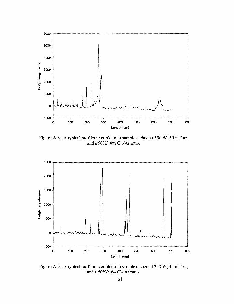
Figure A.8: A typical profilometer plot of a sample etched at 350 W, 30 mTorr,and a 90%/10% C12/Ar ratio.
5000-
4000 -
3000 -
2000 -
1000 -
0
-10000 100 200 300 400 500 600 700 800
Length (um)
Figure A.9: A typical profilometer plot of a sample etched at 350 W, 45 mTorr,and a 50%/50% C12/Ar ratio.
51
CDE
E0
U)(U
LIAIV,

The following optical images were captured on a Carl Zeiss Axiocam MRc digital
camera through a Carl Zeiss Axioplan optical microscope using the 1Ox objective lens.
Figure A.10: Sample etched at 150 W, 20 mTorr, and 90%/10% C12/Ar ratio.
Figure A. 11: Sample etched at 150 W, 30 mTorr, and 50%/50% C12/Ar ratio.
52

Figure A.12: Sample etched at 150 W, 45 mTorr, and 10%/90% C12/Ar ratio.
Figure A. 13: Sample etched at 250 W, 20 mTorr, and 50%/50% C12/Ar ratio
53
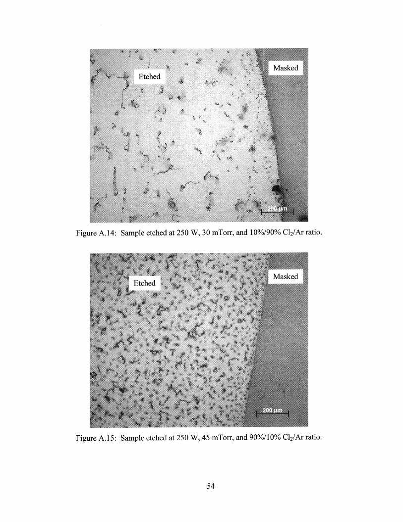
Figure A.14: Sample etched at 250 W, 30 mTorr, and 10%/90% C12/Ar ratio.
Figure A.15: Sample etched at 250 W, 45 mTorr, and 90%/10% C12/Ar ratio.
54

Figure A.16: Sample etched at 350 W, 20 mTorr, and 10%/90% C12/Ar ratio.
Figure A.17: Sample etched at 350 W, 30 mTorr, and 90%/10% C12/Ar ratio.
55

Figure A.18: Sample etched at 350 W, 45 mTorr, and 50%/50% C12/Ar ratio.
Tables A. 1 -A.3 contain raw data of the measured step heights for each sample of
the 3 sets of factorial experiments. The three step height measurements were taken at
random spots along the interface between the masked and etched areas. The average is
the simple mean of the measurements. The settings column refers to the levels of each
factor used in each trial. The first number is the power level, the second is the pressure
setting, and the third is the gas chemistry used. The value of each level can be found in
Table 3.2.
56

Table A. 1: The measurements of step heights found in the samples etchedduring the first set of sensitivity experiments.
Measured step height (A)Settings Site 1 Site 2 Site 3 Average (A)
111 39 18 30 29122 73 43 48 55133 55 43 67 55212 37 73 70 60223 45 66 65 59231 52 55 60 56313 85 112 107 101321 78 65 85 76332 34 51 63 49
Table A.2: The measurements of step heights found in the samples etchedduring the second set of sensitivity experiments.
Measured step height (A)Settings Site 1 Site 2 Site 3 Average (A)
111 32 45 20 32122 27 63 60 50133 55 72 81 69212 87 85 71 81223 67 68 72 69231 63 59 61 61313 145 131 146 141
321 94 78 87 86332 81 104 75 87
57
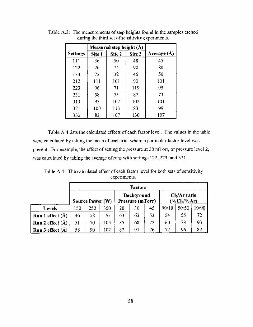
Table A.3: The measurements of step heights found in the samples etchedduring the third set of sensitivity experiments.
Measured step height (A)Settings Site 1 Site 2 Site 3 Average (A)
111 36 50 48 45122 76 74 90 80133 72 32 46 50212 111 101 90 101223 96 71 119 95231 58 73 87 73313 93 107 102 101321 100 113 83 99332 83 107 130 107
Table A.4 lists the calculated effects of each factor level. The values in the table
were calculated by taking the mean of each trial where a particular factor level was
present. For example, the effect of setting the pressure at 30 mTorr, or pressure level 2,
was calculated by taking the average of runs with settings 122, 223, and 321.
Table A.4: The calculated effect of each factor level forexperiments.
both sets of sensitivity
Factors
Source Power (W)Background
Pressure (mTorr)C12/Ar ratio(%C12/%Ar)
Levels 150 250 350 20 30 45 90/10 50/50 10/90
Run 1 effect (A) 46 58 76 63 63 53 54 55 72
Run 2 effect(A) 51 70 105 85 68 72 60 73 93
Run 3 effect(A) 58 90 102 82 91 76 72 96 82
58

Appendix B
Design of experiments
Establishment of the earliest methodological approach to planning and designing
experiments is credited to Sir Ronald A. Fisher. In his approach, he outlined important
aspects of experimental design such as randomization, replication, and the use of factorial
experiments instead of testing the system's response to each factor individually. Fishers
ideas were expanded by Genichi Taguchi and applied to his statistical methods to
improve quality control. Taguchi created a set of standard orthogonal arrays which could
be used to determine the effects that changing certain factors had on a resulting product.
The array used in this research was the L9 array with the modification that the last
column, referring to a fourth factor, was omitted because only three factors were
examined. The modified array is shown in Table B. 1.
The L9 array is referred to as orthogonal based on the balanced combinations of
levels over the full set of runs. In other words, for any pair of factors, every combination
of levels is present exactly once in the nine experiments. Accordingly, each factor level
appears the same total number of times.
Table B. 1: The factor level settings for each run of the matrix experiment asadapted from the L9 Taguchi standard orthogonal array.
Factor
A. Source B. Background C. C12/Ar ratioTrial No. Power level pressure level level
1 1 1 1
2 1 2 2
3 1 3 3
4 2 1 2
5 2 2 3
6 2 3 1
7 3 1 3
8 3 2 1
9 3 3 2
59

Estimation of the factor effects involves simple calculations that take advantage
of the balanced nature of the experimental array. To start off using this research as an
example, the mean, m, is expressed as,
(B.1)
where hi is the step height measured for trial i.
The effect of a factor level can be thought of as the deviation that it causes from
the overall mean as calculated in Equation B. 1. With that in mind, let ai be the deviations
from m caused by the ith level of factor a. Therefore,
A]+A 2+A3=0 (B.2)
where A refers to the factor A, or the power setting for the etch process. Similarly,
B1+B2 +B3=0
C1+C 2+C3=0
(B.3)
(B.4)
where B refers to factor B, the background pressure, and C refers to the ratio of Cl2 to
argon. Furthermore, the observed step height for experiment 6, h6 , can be expressed as,
h 6 =m+A 2 +B 3 +C (B.5)
or the deviation from the mean caused by factor levels A2, B3, and C1. Using this
definition of the observed results of each run, the main effect of any factor level, say
setting pressure at 30 mTorr, can be calculated by,
60
and,
19m=-Lh9H
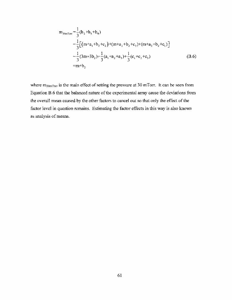
1m30mTorr -(h 2+h5 +h8 )3
= [(m+a, +b2 +c2 )+(m+a 2 +b 2 +c 3 )(m+a 3 +b 2 +c,)]
1 1 1-(3m+3b 2)+ - (a +a2 +a3 )+- (c +c2 +c3 ) (B.6)3 3 3
=m+b2
where m3omTorf is the main effect of setting the pressure at 30 mTorr. It can be seen from
Equation B.6 that the balanced nature of the experimental array cause the deviations from
the overall mean caused by the other factors to cancel out so that only the effect of the
factor level in question remains. Estimating the factor effects in this way is also known
as analysis of means.
61
Bibliography
1. Chen, Francis F., and Jane P. Chang. Lecture Notes on Principles of Plasma
Processing. New York: Kluwer Academic/Plenum Publishers, 2003.
2. Coburn, J. W. and Harold F. Winters. "Ion- and Electron-Assisted Gas-Surface
Chemistry - An Important Effect in Plasma Etching." Journal of Applied Physics
50 (1979): 3189-3196.
3. Dushman, Saul. Scientific Foundations of Vacuum Technique. New York: John
Wiley & Sons, Inc., 1962.
4. Ferrario, B. "Chemical Pumping in Vacuum Technology." Vacuum 47 (1996):
363-370.
5. Howell, John W. "Lamp Developments in America." Electrical World. 85 (1925):
395.
6. Hucknall, David. Vacuum Technology and Applications. Oxford: Butterworth-
Heinemann Ltd., 1991.
7. Imai, Shin-ichi, Hideki Motomura, and Kunihide Tachibana. "Photoresist
Selectivity Mechanism in Si0 2 Etching by Inductively Coupled Plasma Using
Fluorocarbon Gases." Journal of Vacuum Science Technology B 20 (2002): 1482-
1488.
8. Konstantin, Chuntonov. "United States Patent Application Publication No.
US2005/0089627 Al." 28 Apr 2005.
9. Lee, Sangheon, and Yue Kuo. "Chlorine Plasma/Copper Reaction in a New
Copper Dry Etching Process." Journal of the Electrochemical Society 148.9
(2001): G524-G529.
62

10. Matsui, Miyako, Tetsuya Tatsumi, and Makoto Sekine. "Observation of Surface
Reaction Layers Formed in Highly Selective SiO2 Etching." Journal of Vacuum
Science Technology A 19 (2001): 1282-1288.
11. Nguyen, Phucanh, Yuxiao Zeng, and T. L. Alford. "Novel Technique to Pattern
Silver Using CF4 and CF4/0 2 Glow Discharges." Journal of Vacuum Science
Technology B 19 (2001): 158-165.
12. Park, S. D., et al. "Etch Characteristics of Silver by Inductively Coupled Fluorine-
Based Plasmas." Thin Solid Films 445 (2003): 138-143.
13. Phadke, Madhav S. Quality Engineering Using Robust Design. New Jersey:
Prentice Hall, 1989.
14. "Physical Constants of Inorganic Compounds." Handbook of Chemistry and
Physics. 85th Edition, 2004-2005.
15. Power, B. D.. High Vacuum Pumping Equipment. London: Chapman and Hall
Ltd., 1966.
16. Shul, R. J., and S. J. Pearton, eds. Handbook of Advanced Plasma Processing
Techniques. New York: Springer, 2000.
17. Stout, V. L., and M. D. Gibbons. "Gettering of Gas by Titanium." Journal of
Applied Physics. 26 (1955): 1488-1492.
18. Welch, Kimo M. Capture Pumping Technology. 2nd ed. Amsterdam: Elsevier
Science B.V., 2001.
19. Williams, Kirt R., Kishan Gupta, and Matthew Wasilik. "Etch Rates for
Micromachining Processing - Part II." Journal of Microelectromechanical
Systems 12 (2003): 761-778.
63