
A PFC power supply with minimized energy storage ... · A PFC power supply with minimized energy...
107
A PFC power supply with minimized energy storage components and a new control technique for cascaded SMPS by Damien F. Frost A thesis submitted in conformity with the requirements for the degree of Master of Applied Science Graduate Department of Electrical and Computer Engineering University of Toronto Copyright c 2009 by Damien F. Frost
Transcript of A PFC power supply with minimized energy storage ... · A PFC power supply with minimized energy...

A PFC power supply with minimized energy storagecomponents and a new control technique for cascaded
SMPS
by
Damien F. Frost
A thesis submitted in conformity with the requirements
for the degree of Master of Applied ScienceGraduate Department of Electrical and Computer Engineering
University of Toronto
Copyright c© 2009 by Damien F. Frost

Abstract
A PFC power supply with minimized energy storage components and a new control
technique for cascaded SMPS
Damien F. Frost
Master of Applied Science
Graduate Department of Electrical and Computer Engineering
University of Toronto
2009
This Master of Applied Science thesis proposes a new design of low power, power factor
corrected (PFC), power supplies. By lifting the hold up time restriction for devices that
have a battery built in, the energy storage elements of the converter can be reduced,
permitting a small and inexpensive power converter to be built. In addition, a new
control technique for controlling cascaded converters is presented, named duty mode
control (DMC). Its advantages are shown through simulations. The system was proven
using a prototype developed in the laboratory designed for a universal ac input voltage
(85 - 265VRMS at 50 - 60Hz) and a 40W output at 12V . It consisted of two interleaved
phases sensed and digitally controlled on the isolated side of the converter. The prototype
was able to achieve a power factor of greater than 0.98 for all operating conditions, and
input harmonic current distortion well below any set of standards.
ii

To my parents, Sam and Geraldine Frost.
iii

Acknowledgements
I would like to express my gratitude to both of my supervising professors, Professor Peter
Lehn and Professor Aleksandar Prodic, who gave me both the opportunity to study with
them and this exciting project for my thesis. Furthermore, their guidance and support
were invaluable assets that led to the completion of this work.
I also would like to thank all of the fellow students in the SMPS laboratory for their
insight and patience, especially Zdravko Lukic and Amir Parayandeh.
I would also like to acknowledge all of my friends and the members of The Attic for
their constant support and for all of the great memories I have from my graduate studies.
Finally, I would like to thank my family for their unconditional love and support
throughout all of my studies.
iv

Contents
1 Introduction and Background 1
1.1 Background . . . . . . . . . . . . . . . . . . . . . . . . . . . . . . . . . . 2
1.1.1 Simple active PFCs . . . . . . . . . . . . . . . . . . . . . . . . . . 4
1.2 Motivation . . . . . . . . . . . . . . . . . . . . . . . . . . . . . . . . . . . 5
1.3 Literary review . . . . . . . . . . . . . . . . . . . . . . . . . . . . . . . . 6
1.3.1 PFCs . . . . . . . . . . . . . . . . . . . . . . . . . . . . . . . . . . 6
1.3.2 Control of cascaded SMPS . . . . . . . . . . . . . . . . . . . . . . 8
1.4 Objectives . . . . . . . . . . . . . . . . . . . . . . . . . . . . . . . . . . . 8
2 Proposed System 10
2.1 Energy storage in PFCs . . . . . . . . . . . . . . . . . . . . . . . . . . . 11
2.2 New PFC design . . . . . . . . . . . . . . . . . . . . . . . . . . . . . . . 11
2.3 Duty mode control . . . . . . . . . . . . . . . . . . . . . . . . . . . . . . 14
2.4 Centralized digital control . . . . . . . . . . . . . . . . . . . . . . . . . . 14
3 Capacitor Ripple Voltage and Steady State Analysis 15
3.1 Limitations on the capacitor voltage ripple . . . . . . . . . . . . . . . . . 15
3.2 Flyback in steady state . . . . . . . . . . . . . . . . . . . . . . . . . . . . 19
3.2.1 Differential equations of the converter . . . . . . . . . . . . . . . . 19
3.2.2 The flyback converter in steady state . . . . . . . . . . . . . . . . 20
3.2.3 Control for unity power factor operation . . . . . . . . . . . . . . 21
v

3.2.4 A comment on theory . . . . . . . . . . . . . . . . . . . . . . . . 23
4 System Modeling and Control 25
4.1 Duty mode control (DMC) . . . . . . . . . . . . . . . . . . . . . . . . . . 25
4.1.1 Advantages of DMC . . . . . . . . . . . . . . . . . . . . . . . . . 25
4.1.2 Two stage DMC example . . . . . . . . . . . . . . . . . . . . . . . 27
4.1.3 DMC model with downstream PID compensator . . . . . . . . . . 30
4.1.4 State space model . . . . . . . . . . . . . . . . . . . . . . . . . . . 31
4.1.5 Control to output transfer function . . . . . . . . . . . . . . . . . 33
4.1.6 DMC vs. conventional control . . . . . . . . . . . . . . . . . . . . 35
4.2 System models . . . . . . . . . . . . . . . . . . . . . . . . . . . . . . . . 38
4.2.1 Lossy buck converter in state space . . . . . . . . . . . . . . . . . 38
4.2.2 Lossy flyback converter in state space . . . . . . . . . . . . . . . . 38
4.2.3 Additional parts of the system model . . . . . . . . . . . . . . . . 45
4.2.4 Complete system model in state space . . . . . . . . . . . . . . . 48
4.3 Controller design . . . . . . . . . . . . . . . . . . . . . . . . . . . . . . . 54
4.3.1 Voltage controller design for buck converter . . . . . . . . . . . . 54
4.3.2 Current controller design for the flyback converter . . . . . . . . . 56
4.3.3 DMC controller design for the flyback converter . . . . . . . . . . 58
5 Experimental Results 62
5.1 Flyback component selection . . . . . . . . . . . . . . . . . . . . . . . . . 62
5.1.1 Flyback transformer . . . . . . . . . . . . . . . . . . . . . . . . . 62
5.1.2 Main energy storage capacitor . . . . . . . . . . . . . . . . . . . . 63
5.2 Converter specifications . . . . . . . . . . . . . . . . . . . . . . . . . . . 64
5.3 Steady state operation . . . . . . . . . . . . . . . . . . . . . . . . . . . . 64
5.4 Power factor and THD . . . . . . . . . . . . . . . . . . . . . . . . . . . . 67
5.5 Transient response . . . . . . . . . . . . . . . . . . . . . . . . . . . . . . 69
vi

5.6 Energy storage comparison . . . . . . . . . . . . . . . . . . . . . . . . . . 70
5.7 Limitations of the proposed system . . . . . . . . . . . . . . . . . . . . . 71
5.7.1 Current measurement . . . . . . . . . . . . . . . . . . . . . . . . . 71
5.7.2 Loss in main energy storage capacitor . . . . . . . . . . . . . . . . 72
5.7.3 Hold up time . . . . . . . . . . . . . . . . . . . . . . . . . . . . . 73
6 Conclusions and Future Work 76
6.1 Conclusions . . . . . . . . . . . . . . . . . . . . . . . . . . . . . . . . . . 76
6.2 Future work . . . . . . . . . . . . . . . . . . . . . . . . . . . . . . . . . . 77
6.2.1 PFC supplies with minimized energy storage . . . . . . . . . . . . 77
6.2.2 DMC . . . . . . . . . . . . . . . . . . . . . . . . . . . . . . . . . . 77
6.2.3 On chip integration . . . . . . . . . . . . . . . . . . . . . . . . . . 78
Appendices 80
A Circuit Schematic 80
A.1 Circuit schematics . . . . . . . . . . . . . . . . . . . . . . . . . . . . . . 80
A.2 Bill of materials . . . . . . . . . . . . . . . . . . . . . . . . . . . . . . . . 88
B Measurement Devices 89
Bibliography 94
vii

List of Tables
3.1 Parameters of the flyback converter simulation . . . . . . . . . . . . . . . 23
4.1 Parameters used to compare DMC and conventional control. . . . . . . . 35
4.2 Parameters used in the buck converter developed in lab. . . . . . . . . . 55
4.3 Parameters used in the flyback converter developed in lab. . . . . . . . . 57
4.4 Parameters from the laboratory used in the complete system model. . . . 59
5.1 Technical specifications for the main energy storage capacitor. . . . . . . 63
5.2 Technical specifications of the main energy storage capacitor . . . . . . . 63
5.3 Performance specifications of the converter designed in the laboratory. . . 64
5.4 Technical specifications of each phase of the converter . . . . . . . . . . . 65
5.5 Voltage ripple on the main energy storage capacitor . . . . . . . . . . . . 67
5.6 Energy storage comparison . . . . . . . . . . . . . . . . . . . . . . . . . . 71
B.1 Table of measurement devices used. . . . . . . . . . . . . . . . . . . . . . 89
viii

List of Figures
1.1 The traditional diode bridge rectifier used as an ac to dc power supply. . 3
1.2 The voltage and current waveforms of the diode bridge rectifier . . . . . . 3
1.3 Topology of the flyback converter. . . . . . . . . . . . . . . . . . . . . . . 4
1.4 The averaged switch model of the flyback converter in DCM. . . . . . . . 4
2.1 A typical two stage PFC supply. . . . . . . . . . . . . . . . . . . . . . . . 12
2.2 Topology of the proposed system. . . . . . . . . . . . . . . . . . . . . . . 13
2.3 Block diagram depicting DMC. . . . . . . . . . . . . . . . . . . . . . . . 14
3.1 The ripple current in the capacitor . . . . . . . . . . . . . . . . . . . . . 16
3.2 The ac power absorbed by the storage capacitor . . . . . . . . . . . . . . 18
3.3 The flyback converter with the main switch, Q1, on. . . . . . . . . . . . . 19
3.4 The flyback converter with the main switch, Q1, off. . . . . . . . . . . . . 19
3.5 Flyback operating at unity power factor simulation . . . . . . . . . . . . 24
4.1 Block diagram depicting DMC. . . . . . . . . . . . . . . . . . . . . . . . 26
4.2 Converter used to illustrate DMC. . . . . . . . . . . . . . . . . . . . . . . 28
4.3 The linearized model of the buck converter with losses. . . . . . . . . . . 29
4.4 Complete model of two converters in series to show the properties of DMC. 31
4.5 Transfer functions of DMC vs. conventional control . . . . . . . . . . . . 36
4.6 Step response simulation of conventional control vs. DMC . . . . . . . . 37
4.7 The buck converter with losses and switching network shown. . . . . . . 38
ix

4.8 The flyback converter with losses. . . . . . . . . . . . . . . . . . . . . . . 39
4.9 A PI controller in state space. . . . . . . . . . . . . . . . . . . . . . . . . 48
4.10 The complete small signal model of the system. . . . . . . . . . . . . . . 48
4.11 Bode plot of GBvc (s) . . . . . . . . . . . . . . . . . . . . . . . . . . . . . . 55
4.12 Compensated bode plot of GBvc (s) . . . . . . . . . . . . . . . . . . . . . . 56
4.13 Bode plot of GAic (s) . . . . . . . . . . . . . . . . . . . . . . . . . . . . . . 58
4.14 Compensated bode plot of GAic (s) . . . . . . . . . . . . . . . . . . . . . . 59
4.15 Bode plot of DMC transfer function . . . . . . . . . . . . . . . . . . . . . 60
4.16 Compensated bode plot of DMC transfer function . . . . . . . . . . . . . 61
5.1 input voltage and current of prototype . . . . . . . . . . . . . . . . . . . 65
5.2 Voltage of energy storage capacitor while operating at full load . . . . . . 66
5.3 Comparing the theoretical and experimental duty cycles. . . . . . . . . . 67
5.4 The measured power factor of the converter developed in the laboratory. 68
5.5 The THD of the prototype converter . . . . . . . . . . . . . . . . . . . . 68
5.6 Harmonic current emissions from the prototype vs. IEC61000-3-2 . . . . 69
5.7 Transient response of the prototype - load increase . . . . . . . . . . . . . 70
5.8 Transient response of the prototype - load decrease . . . . . . . . . . . . 70
5.9 Current sensing waveform . . . . . . . . . . . . . . . . . . . . . . . . . . 72
5.10 The CBEMA Curve [1]. . . . . . . . . . . . . . . . . . . . . . . . . . . . 74
5.11 Hold up time of the prototype . . . . . . . . . . . . . . . . . . . . . . . . 75
A.1 Overall circuit schematic of the converter built in the laboratory. . . . . . 81
A.2 Circuit schematic for the ADCs, ADC circuit.SchDoc. . . . . . . . . . . . 82
A.3 Circuit schematic for the linear regulators, LinearRegulator.SchDoc. . . . 83
A.4 Circuit schematic for the non inverting operational amplifier . . . . . . . 84
A.5 Circuit schematic for the power stage, PowerStage.SchDoc. . . . . . . . . 85
A.6 Circuit schematic of the gate drivers, GateDriver.SchDoc. . . . . . . . . . 86
x

A.7 Circuit schematic for the inverting operational amplifiers . . . . . . . . . 87
A.8 Bill of materials for one phase of the power stage. . . . . . . . . . . . . . 88
xi

List of Abbreviations
ac Alternating CurrentADC Analog to Digital Converter
CBEMA Computer and Business Equipment Manufacturers AssociationCCM Continuous Conduction Mode
dc Direct CurrentDCM Discontinuous Conduction ModeDMC Duty Mode Control
DPWM Digital Pulse Width ModulatorESR Equivalent Series ResistanceFFT Fast Fourier Transform
FPGA Field Programmable Gate ArrayIC Integrated Circuit
ICS Input Current ShaperIEC International Electrotechnical Commission
IEEE Institute of Electrical and Electronics EngineersIT Information Technology
ITIC Information Technology Information CouncilPF Power Factor
PFC Power Factor CorrectionPI Proportional Integral
PID Proportional Integral DifferentialRMS Root Mean Square
SMPS Switch Mode Power SupplyTHD Total Harmonic Distortion
xii

Notation
X (t), x (t) time dependent quantity〈x (t)〉Ts time averaged quantity over period Ts
x small signalX dc signal or constant quantityX constant matrix or vectorx vector of small signals
X (s) continuous time transfer functionx [n] discrete time quantity
xiii

Chapter 1
Introduction and Background
This chapter introduces the main topic of this work, low power, power factor corrected
(PFC), power supplies. In this area, two main foci will be addressed. First, the reduction
of the size of energy storage elements in PFC supplies and second, a new control method
to control cascaded switch-mode power supplies.
The size of energy storage elements in the converter is reduced by allowing a large
ripple voltage to appear on the main energy storage capacitor, greatly reducing the size
of this component. This ripple voltage is as much as 37% of the nominal value.
The new control method proposed utilizes the duty cycle of the downstream converter
to control the output voltage of the upstream stage. This reduces the number of sensors
required by one, and also provides a better transient response.
First a brief introduction to power factor correction is presented, followed by the
motivation of this work. A review of existing solutions is then presented and the chapter
concludes with the goals of this thesis.
The rest of the work is organized as follows:
Chapter 2 contains a description of the proposed system and describes its novel as-
pects.
Chapter 3 demonstrates how to use a capacitor in a PFC to its designed limits,
1

Chapter 1. Introduction and Background 2
utilizing its full energy storage capabilities.
Chapter 4 models the proposed system in state space and introduces a new control
method for cascaded converters, duty mode control (DMC). From this model, controllers
are designed for the proposed system that are verified in the laboratory.
Chapter 5 shows the results from the prototype converter built in the laboratory.
Chapter 6 summarizes the results from this work and suggests future directions that
can be investigated.
1.1 Background
Power factor is a measure of how effectively energy is transmitted between a source and
a load in a system. From [2] there are two different definitions for power factor and these
are shown in Equations (1.1) and (1.2). Equation (1.1) calculates the power factor in
the presence of harmonics in either the supply voltage or supply current. Equation (1.2)
calculates the power factor assuming the voltage and current are purely sinusoidal and
is only a function of the angle between the voltage phasor and current phasor, φ.
(power factor)1 =(average power)
(rms voltage) (rms current)(1.1)
(power factor)2 = cos (φ) (1.2)
For this work, Equation (1.1) will be used to calculate the power factor. Both equa-
tions stipulate that the power factor is a value between zero and one, and in order to
have the most efficient energy transmitting network, a power factor of one is necessary.
However, this only occurs when the load is a perfect resistor. Other loads such as reactive
and non linear loads introduce imaginary power and distortion into the system and will
cause current to flow from the source to the load and back again without doing any real

Chapter 1. Introduction and Background 3
Figure 1.1: The traditional diode bridge rectifier used as an ac to dc power supply.
0 0.005 0.01 0.015 0.02 0.025 0.03
Source Voltage
Time (s)V
olta
ge
0 0.005 0.01 0.015 0.02 0.025 0.03
Source Current
Time (s)
Cur
rent
Figure 1.2: The voltage and current waveforms of the diode bridge rectifier of Figure 1.1
work. This additional current requires all the components in the system to have higher
ratings and it also contributes to the heating of power transformers and transmission
lines. Therefore, it would be ideal if all loads had a power factor of one. For this reason,
many high power, and now low power, loads are required to meet government regula-
tions on current harmonic limits through standards set by the institute of Electrical and
Electronics Engineers (IEEE) and the International Electrotechnical Commission (IEC).
An example of such a non linear load is the traditional diode bridge rectifier, shown
in Figure 1.1, used as an ac to dc power supply. This circuit is highly non linear and the
current and voltage waveforms are shown in Figure 1.2. The power factor of this circuit
is typically around 0.55 to 0.65 [2].
The power factor of the diode bridge rectifier circuit can be improved either passively
or actively. A passive solution is to add a filter to the input of the diode bridge. This is
rarely done in practice, as the filter required would be large, expensive and would only
work for a certain input frequency. The second way to improve the power factor of this
circuit is to add a switching network after the diode bridge to regulate the input current.

Chapter 1. Introduction and Background 4
1:n
C1
Q1
D1
D
R
Figure 1.3: Topology of the flyback converter.
C1
D
RTnD
L22
2
p(t) T
Figure 1.4: The averaged switch model of the flyback converter in DCM.
This is commonly implemented and is discussed in greater detail in the next section.
1.1.1 Simple active PFCs
Simple active PFCs are circuits that emulate an ideal resistance when attached to an ac
system. The analysis of power converters based on average switch modeling [2], shows
that many common topologies are natural PFCs when operated in the discontinuous
conduction mode (DCM), without additional control. These converters include the buck-
boost, flyback, SEPIC and Cuk [2]. Therefore, using one of these converters as a PFC
is a simple choice. Figure 1.4 shows the averaged switch model of the flyback converter
of Figure 1.3. As shown, the input port of the converter is modeled as a lossless resistor
whose power is transferred over to the power source, connecting the load. The duty cycle
of the boost converter simply changes the value of the loss-less resistor to either increase
or decrease the input, and by consequence the output, power.
Although theoretically very effective, in a practical implementation of this system an

Chapter 1. Introduction and Background 5
electromagnetic interference (EMI) filter will be required to filter out the discontinuous
input current.
1.2 Motivation
Until recently, power factor correction has been limited to high power loads, through
standards like IEEE519 [3]. However in 2001 the European Union adopted the Inter-
national Electro-Technical Commission’s IEC61000-3-2 standard for electrical equipment
which puts harmonic current limits on all devices that draw up to 16A and consume more
than 75W in a 220V ac system [4]. Since then, Britain, China and Japan have adopted
similar standards [5].
These standards have yet to be adopted for North America, however one can assume
that they will be at least as strict as the IEC61000-3-2 in the near future. The inconsis-
tency in restrictions is due to the differences between the European and North American
distribution systems. North American distribution systems are predominantly a wye-wye
system and therefore, are more susceptible to triplen harmonics (3rd, 9th, 15th, etc.).
As a result, any limitations that might be imposed in North America will most likely be
very different from those set in the IEC61000-3-2 standard [6].
Furthermore, the restrictions are being applied to lower power devices most likely be-
cause there are an increasing number of highly non-linear loads being used by consumers
everyday, as seen in Canada [7], [8]. If all of the ac-dc power supplies found in an average
household were implemented with the diode bridge rectifier of Figure 1.1, the spikes in
the current generated by these circuits would not go unnoticed.
Finally, there are significant indications that there will be a market for inexpensive,
low power, PFC supplies. This work will fill this area by proposing a solution that
provides power factor correction with minimized energy storage elements, thus producing
lower cost, more compact power supplies.

Chapter 1. Introduction and Background 6
1.3 Literary review
1.3.1 PFCs
As shown in [9], PFC converters can be categorized into two main groups: sinusoidal line
current and non-sinusoidal line current. Converters with a non-sinusoidal line current
are the converters that meet harmonic specifications like the IEC61000-3-2, however
they may not be able to meet future harmonics specifications. Therefore, the discussion
here focuses on sinusoidal line current PFC converters.
1.3.1.1 The boost PFC
The boost topology operating in discontinuous conduction mode (DCM) is one of the
most natural PFC topologies. However, it has a few drawbacks, two of which are outlined
here. First, the energy storage capacitor must be able to handle voltages above the peak
line voltage of any input. Second, the input current harmonics are fairly high because
the current goes to zero after every switching cycle, putting more stress on the input
filter of the converter [10].
A reduction of voltage stresses on the main energy storage capacitor of the boost
converter has been achieved through a modified boost topology as presented in [11]. The
topology is called “The series inductance interval” and it is able to achieve a low voltage
on the storage capacitor as well as a low voltage swing depending on the input voltage.
A more detailed analysis of this converter and an improved version is presented in [12].
Many solutions to reduce the input current switching harmonics have also been pro-
posed and a common solution is to interleave many boost cells into a converter. By
using two cells one can reduce the switching harmonics by half [10] or eliminate them
completely with a slight modification to the boost topology as demonstrated in [13]. Fur-
thermore, [14] provides a solution to optimize the number of boost cells to use based on
the design specifications of the converter.

Chapter 1. Introduction and Background 7
Many variations of the topology have been developed in order to improve its perfor-
mance. Reference [15] provides a good survey of single stage PFC circuits with a boost
type input current shaper (ICS). In this review, many different topologies are examined
and are grouped into two categories of converters: converters with a two terminal ICS
cell and converters with a three terminal ICS cell. These two categories of ICSs are also
consistent with grouping of boost ICSs in [16].
1.3.1.2 The flyback PFC
As shown in [17] and [18], the flyback converter is one of the best topologies that is able to
achieve near unity power factor as well as direct power transfer to the load. Furthermore,
in comparison to the PFC boost, the flyback converter electrically isolates the ac and dc
sides. However, just like the boost converter, much research has been published analyzing
its performance [19], [20] and improving aspects of the converter. The flyback has also
been combined with other topologies to create novel single stage converters, as mentioned
in [15].
1.3.1.3 Digital control of PFC converters
Digital control of converters is becoming the preferred option for designers because it
allows for more flexible designs, shorter development times, the elimination of tuning
discrete components and increased reliability [21].
There have been many works published on the digital control of PFC converters like
the one shown in [22]. Therefore the digital control of PFC converters has been shown
to be successful.
To completely design a digital controller, an extremely useful resource is [23]. In
this work the authors give a complete overview of designing a digital controller. A good
complement to this work is [24], where three different digital control design techniques
are compared experimentally.

Chapter 1. Introduction and Background 8
1.3.1.4 Reducing the size of energy storage components
In the literature, all of the PFC topologies are designed such that they meet the hold up
time standard set by the Information Technology Industry Council (ITIC) [1]. However,
this hold up time was designed for devices that do not have a battery built in. Devices that
would benefit from a smaller PFC supply are those designed for portability, for example
laptops and battery chargers. Furthermore, one can expect these devices to be more
prevalent in the future considering for the first time in 2008, worldwide laptop sales have
outpaced those of desktop sales [25]. Devices such as laptops and battery chargers are
low power electronics that will likely have to abide by input current harmonic limits set
by governments. They are also devices that can withstand a temporary fault in the power
system quite easily because battery charging can be interrupted without consequence,
just as it can in a laptop since it contains a battery built in. Furthermore, smaller and
lighter power supplies are more desirable and usually must be taken along with the device
they power.
1.3.2 Control of cascaded SMPS
The discussion around the control and stability analysis of cascaded switch mode power
supplies (SMPS) has been largely limited to defining impedance criteria which the power
supplies must meet in order to preserve stability [26], [27], [28].
1.4 Objectives
The main goal of this work is to create a prototype of a low power, PFC supply, suitable
for portable electronic applications where the hold up time is not a necessity.
The objectives of this work are as follows:
• Reduce the size of energy storage components in the converter by increasing the

Chapter 1. Introduction and Background 9
switching frequency, allowing a large ripple voltage on the main energy storage
capacitor and creating an integrated design of the system.
• Introduce a new method for controlling cascaded SMPS and combine all the con-
trollers of the system into a single FPGA.
• Exploit low cost and low voltage components by appropriately designing the power
stages.

Chapter 2
Proposed System
This chapter introduces the proposed system. It consists of two parallel converter systems
operated with interleaved switching, to reduce input current switching harmonics. These
are referred to as interleaved phases. Each phase is rated for a 20W load and consists
of a flyback converter connected in series with a buck converter. The flyback acts as a
power factor corrector in the system, and its output capacitor is the main energy storage
component of the system. This capacitor is targeted for size reduction. As a consequence,
a large ripple voltage on this capacitor exists with a nominal value around 50V dc. The
buck converter acts as a constant power load on the flyback converter, outputting a
regulated 12V dc. The total output power of the system is rated for a 40W load. The
system was designed for low power PFC applications where hold up time is not critical.
However, being an interleaved system, more phases could be added to increase the output
power to the desired amount.
The rest of the chapter will introduce the main problem with unity power factor ac/dc
conversion, followed by the proposed converter topology. It will conclude by introducing
a novel control method for controlling cascaded converters.
10

Chapter 2. Proposed System 11
2.1 Energy storage in PFCs
One of the largest problems PFC supplies face when powering a dc load is dealing with
the second harmonic power ripple. The problem may be understood by studying the
power entering a PFC, as shown in Equation (2.1) below.
Pac (t) = Vg cos (ωt) Ig cos (ωt) =VgIg
2(1 + cos (2ωt)) (2.1)
From this equation it is clear that the input power into a PFC supply contains a
second harmonic ripple component. The output dc power is defined by the average value
of Equation (2.1) over a period, (VgIg) /2. During times when the input power is less
than the output power, the PFC must have sufficient energy storage to supply the dc
load. Providing this power is conventionally done with a large capacitor, and in the case
of a boost converter acting as a PFC operating in CCM, a large high voltage capacitor.
A capacitor of this type is very large, bulky and expensive. Moreover, its energy storage
capabilities are under utilized. In the proposed solution the capacitor will be reduced in
size so as to maximize the use of its energy storage capabilities. As a consequence, there
will be a large ripple voltage on the main energy storage capacitor of the system at twice
the frequency of the line voltage and this will introduce control challenges that have not
previously been addressed.
2.2 New PFC design
Traditional PFC supplies comprise of two stages [29] and require sensing and control on
the non-isolated, ac side as well as the isolated side for any downstream converter. An
example is shown in Figure 2.1.
The design of these power supplies is such that the output voltage of the PFC, the
voltage on capacitor C1 in Figure 2.1, remains relatively constant. This requires a large,

Chapter 2. Proposed System 12
T1
Vg LoadC2C1
Q2
Q3
Q1
D1
PFCController
VoltageController
Main EnergyStorage
Capacitor
Ig
Figure 2.1: A typical two stage PFC supply.
expensive, and in the case of boost converter acting as a PFC in CCM, a high volt-
age capacitor as the main storage element. The proposed PFC design eliminates these
requirements on the main energy storage capacitor.
The topology of the proposed system was chosen such that a few basic criteria could
be met:
• Galvanic isolation
• Universal input voltage (85 - 265Vrms at 50 − 60Hz)
• Convenient output voltage for household electronics (12V )
In addition, the topology was chosen such that other novel criteria could be met,
which would also reduce the cost and size of the converter:
• A small, low voltage energy storage capacitor
• A single, centralized controller
• Reduced voltages in the converter
Taking these points into account, a conventional topology of a series connection of a
flyback and buck converter was chosen as shown in Figure 2.2.
Both converters operate in continuous conduction mode (CCM) to reduce peak cur-
rents in the system. To decrease the switching harmonics, an interleaved, two phase PFC
stage was implemented.

Chapter 2. Proposed System 13
1:0.32
Vg LoadC2C1
Q2
Q3
Q1
D1
PFC and VoltageController
Main EnergyStorage Capacitor
Ig
Figure 2.2: Topology of the proposed system.
The turns ratio on the flyback transformer was chosen to provide a step down in
voltage. This allows the main energy storage capacitor of the system, C1 in Figure 2.2,
to be an inexpensive, low voltage component. The turns ratio chosen for the system was
1 : 0.32.
Isolation is maintained through the use of a single optical coupler to send a gating
pulse to the main switch, Q1.
Finally, a significant innovation in the proposed converter is the location of input
current and voltage sensors. Both sensors are placed on the secondary side of the trans-
former, allowing all sensing and control to be done on this side. Voltage sensing is
accomplished when the main switch Q1 is in the on state. During this time, the voltage
across the primary side of the transformer is reflected to the secondary side and thus can
be read by a sensor. Current sensing is accomplished when the main switch turns off,
forcing the magnetizing current of the flyback transformer to flow through the secondary
side, and therefore through the sensing resistor. In this way the controller can be com-
bined into a single chip, as shown in Figure 2.2. As shown in Chapter 4, this will allow
us to further reduce the size of the energy storage capacitor.
Chapter 2. Proposed System 14
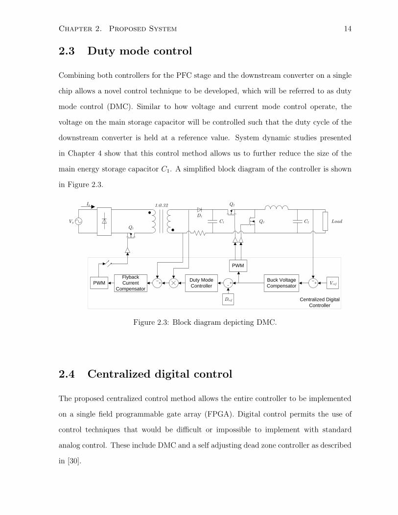
2.3 Duty mode control
Combining both controllers for the PFC stage and the downstream converter on a single
chip allows a novel control technique to be developed, which will be referred to as duty
mode control (DMC). Similar to how voltage and current mode control operate, the
voltage on the main storage capacitor will be controlled such that the duty cycle of the
downstream converter is held at a reference value. System dynamic studies presented
in Chapter 4 show that this control method allows us to further reduce the size of the
main energy storage capacitor C1. A simplified block diagram of the controller is shown
in Figure 2.3.
Centralized DigitalController
1:0.32
Vg LoadC2C1
Q2
Q3
Q1
D1
VrefBuck VoltageCompensator
PWM
Duty ModeController
FlybackCurrent
CompensatorPWM
Dref
Ig
Figure 2.3: Block diagram depicting DMC.
2.4 Centralized digital control
The proposed centralized control method allows the entire controller to be implemented
on a single field programmable gate array (FPGA). Digital control permits the use of
control techniques that would be difficult or impossible to implement with standard
analog control. These include DMC and a self adjusting dead zone controller as described
in [30].

Chapter 3
Capacitor Ripple Voltage and
Steady State Analysis
This chapter begins by deriving an equation that allows one to use an energy storage
capacitor to its designed limits. Following this, the steady state analysis of the flyback
converter powering a dc load at unity power factor is carried out. In particular, the
consequences of allowing a large ripple voltage on its capacitor are studied.
3.1 Limitations on the capacitor voltage ripple
First, an expression for the ripple voltage on the capacitor is derived based on the rated
ripple current the capacitor can handle, Ir, which is measured in amps rms.
Figure 3.1 shows the ripple current in the capacitor. The shaded region is the amount
of charge, ΔQ, that is deposited onto the capacitor when the current is positive. This
charge is added to the charge residing on the capacitor when it is at its lowest voltage,
VMIN . Therefore the maximum voltage on the capacitor is given by Equation (3.1):
VMAX =QMIN + ΔQ
C(3.1)
15
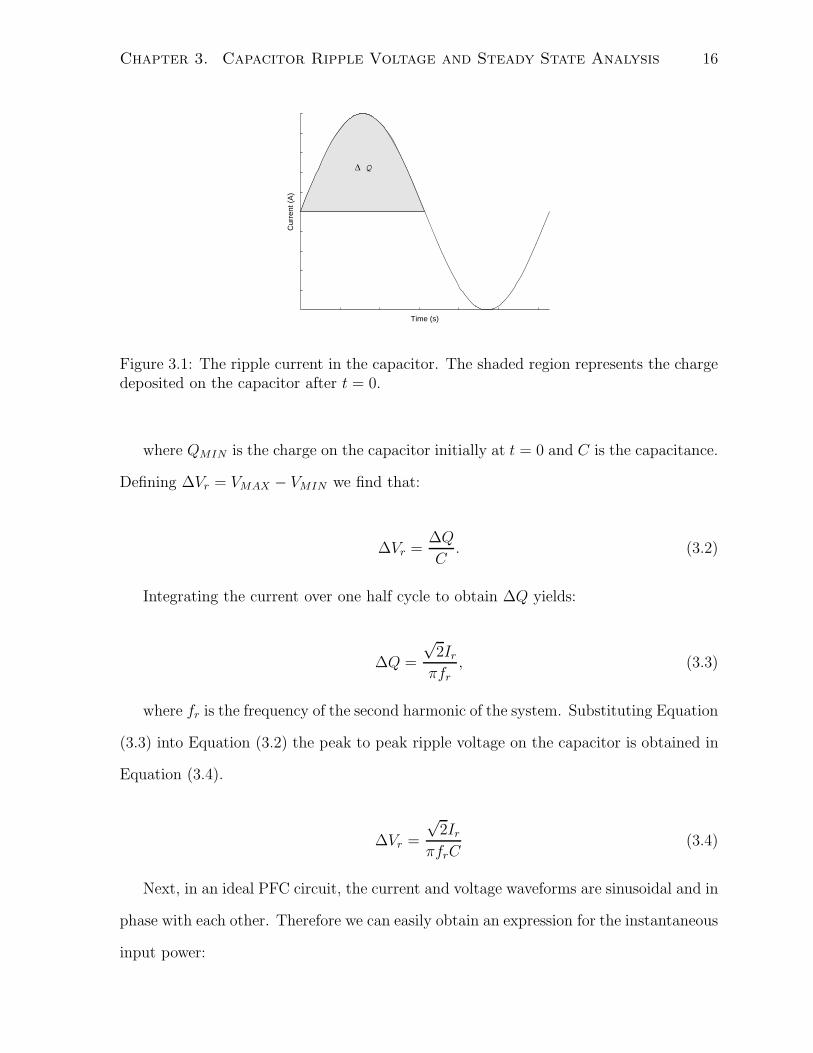
Chapter 3. Capacitor Ripple Voltage and Steady State Analysis 16
Time (s)
Cur
rent
(A
)
Δ Q
Figure 3.1: The ripple current in the capacitor. The shaded region represents the chargedeposited on the capacitor after t = 0.
where QMIN is the charge on the capacitor initially at t = 0 and C is the capacitance.
Defining ΔVr = VMAX − VMIN we find that:
ΔVr =ΔQ
C. (3.2)
Integrating the current over one half cycle to obtain ΔQ yields:
ΔQ =
√2Ir
πfr, (3.3)
where fr is the frequency of the second harmonic of the system. Substituting Equation
(3.3) into Equation (3.2) the peak to peak ripple voltage on the capacitor is obtained in
Equation (3.4).
ΔVr =
√2Ir
πfrC(3.4)
Next, in an ideal PFC circuit, the current and voltage waveforms are sinusoidal and in
phase with each other. Therefore we can easily obtain an expression for the instantaneous
input power:

Chapter 3. Capacitor Ripple Voltage and Steady State Analysis 17
Pin (t) = Vg cos (ωt) Ig cos (ωt) =VgIg
2(1 + cos (2ωt)) (3.5)
where ω is the line frequency.
Equation (3.5) can be separated into a dc and ac component yielding:
Pin (t) = Pdc + Pac (t) (3.6)
where,
Pdc =VgIg
2(3.7)
and
Pac (t) =VgIg
2cos (2ωt) = Pdc cos (2ωt) . (3.8)
Assuming that the ac component of the input power is absorbed completely by the
storage capacitor, we can determine the ripple on the capacitor that will result in this
oscillating power. This assumption is valid as long as the magnetizing inductance and
current are small enough such that 0.5LmI2m << 0.5C1V
2C .
The shaded region in Figure 3.2 represents the energy absorbed by the capacitor for
one half cycle. This absorption of energy will increase the capacitor voltage according to
Equation (3.9). Let this energy be called ΔE.
ΔE =1
2C
(V 2
f − V 2i
)(3.9)
where Vf , Vi and C are the final capacitor voltage, initial capacitor voltage and the
capacitance, respectively.
Integrating the ac power over a half cycle to obtain ΔE yields:

Chapter 3. Capacitor Ripple Voltage and Steady State Analysis 18
Time (s)P
ower
(W
)
Δ E
PDC
Figure 3.2: The ac power absorbed by the storage capacitor. The shaded region representsthe energy absorbed by the capacitor during one half cycle.
ΔE =Pdc
ω. (3.10)
Now substitute Equation (3.10) into Equation (3.9) and let Vi = VMAX − ΔVr and
Vf = VMAX :
Pdc =1
2Cω
(2VMAXΔVr − ΔV 2
r
). (3.11)
Finally substituting Equation (3.4) into Equation (3.11) for ΔVr yields the final result:
Pdc =√
2VMAXIr − I2r
πfrC. (3.12)
Equation (3.12) is an expression for the maximum dc power one can draw from an ac
source at unity power factor while effectively filtering out the ac ripple power and using
the capacitor to its designed limits.

Chapter 3. Capacitor Ripple Voltage and Steady State Analysis 19
3.2 Flyback in steady state
This section goes through the analysis of the flyback converter, which is the first stage in
each phase. This converter will be considered in steady state when it provides constant
power for a dc load at unity power factor. First, the time averaged differential equations
for the converter are found and a solution for the duty cycle is solved for.
3.2.1 Differential equations of the converter
To find the time averaged differential equations of the converter in CCM, the converter
is analyzed in its two possible states, as shown in Figures 3.3 and 3.4.
1:n
CVg
Q1
D1Lm ilV
ig
icim
Figure 3.3: The flyback converter with the main switch, Q1, on.
1:n
CVg
Q1
D1Lm ilV
ig
icim
Figure 3.4: The flyback converter with the main switch, Q1, off.
When the transistor is on (depicted as an ideal switch Q1 in the figure) the voltage
across the magnetizing inductance is vg and its current is ig. The output capacitor current
is simply the load current, il. When the transistor is off, the diode (ideal switch D1 in the
figure) conducts and the voltage across the magnetizing inductance becomes −v/n. The

Chapter 3. Capacitor Ripple Voltage and Steady State Analysis 20
output capacitor current is the difference in the current in the magnetizing inductance
reflected to the secondary side minus the load current, im/n−il. The differential equations
representing the system become Equations (3.13) - (3.15).
Ldim (t)
dt=
⎧⎪⎨⎪⎩
vg (t)
−v(t)n
0 < t ≤ d (t) Tsw
d (t)Tsw < t ≤ Tsw
(3.13)
Cdv (t)
dt=
⎧⎪⎨⎪⎩
−il (t)
im(t)n
− il (t)
0 < t ≤ d (t) Tsw
d (t)Tsw < t ≤ Tsw
(3.14)
ig (t) =
⎧⎪⎨⎪⎩
im (t)
0
0 < t ≤ d (t) Tsw
d (t)Tsw < t ≤ Tsw
(3.15)
Averaging these equations over one period yields the large signal time averaged non-
linear differential equations of the flyback converter, shown below.
Ld 〈im (t)〉Ts
dt= d (t) 〈vg (t)〉Ts − (1 − d (t))
〈v (t)〉Ts
n(3.16)
Cd 〈v (t)〉Ts
dt= (1 − d (t))
〈im (t)〉Ts
n− 〈il (t)〉Ts (3.17)
〈ig (t)〉Ts = d (t) 〈im (t)〉Ts (3.18)
3.2.2 The flyback converter in steady state
To obtain the equations for the steady state operation of the flyback converter in CCM,
the small ripple approximation can be applied to Equation (3.16) and the principle of
charge balance to Equation (3.17). This yields the following relationships:

Chapter 3. Capacitor Ripple Voltage and Steady State Analysis 21
V
Vg= n
D
(1 − D), (3.19)
IM =nIl
(1 − D). (3.20)
Equation (3.19) can be solved for the duty cycle:
D =V
nVg + V. (3.21)
3.2.3 Control for unity power factor operation
The flyback converter will operate with unity power factor when the input current is in
phase with the input voltage. The duty cycle of the converter can be solved for using
this constraint.
3.2.3.1 Output voltage of the flyback
At unity power factor, the input power is:
Pin (t) = VgIg
(1 + cos (2ωt)
2
). (3.22)
Assuming that the flyback converter is ideal and the downstream converter is pow-
ering a dc load, the power delivered by the flyback is the dc component: VgIg/2. The
second, ac, term is the power that must be absorbed by the filtering elements of the fly-
back. Additionally by noticing that the capacitor has significantly more energy storage
capability than the inductor as shown in Equation (3.23), it will again be assumed that
all of the ac power will be absorbed by the capacitor. This is shown in Equation (3.24).

Chapter 3. Capacitor Ripple Voltage and Steady State Analysis 22
LI2L � CV 2 (3.23)
v (t) ic (t) =VgIg cos (2ωt)
2(3.24)
where ic is the current in the capacitor and can be replaced with the differential
equation which governs the behavior of a capacitor as shown in Equation (3.25).
v (t)dv (t)
dtC =
VgIg cos (2ωt)
2. (3.25)
Equation (3.25) is a separable differential equation and can be solved by integration,
resulting in Equation (3.28).
∫v (t) dv =
∫VgIg cos (2ωt)
2Cdt (3.26)
1
2v (t)2 =
VgIg sin (2ωt)
4ωC+
V 20
2(3.27)
v (t) =
√VgIg sin (2ωt)
2ωC+ V 2
0 (3.28)
where V0 is the constant of integration and is the voltage of the capacitor at t = 0.
Equation (3.28) defines the voltage that must exist on the output capacitor of the flyback
converter during unity power factor operation. This equation assumes that all the ac
power is absorbed by this capacitor and the flyback converter is powering a dc load.
3.2.3.2 Duty cycle of the flyback
Combining Equation (3.28) and Equation (3.21), we can find the duty cycle needed to
achieve unity power factor when operating in CCM. The result is shown in Equation
(3.29).

Chapter 3. Capacitor Ripple Voltage and Steady State Analysis 23
Dflyback (t) =
√VgIg sin(2ωt)
2ωC+ V 2
0
n |Vg cos (ωt)| +√
VgIg sin(2ωt)2ωC
+ V 20
(3.29)
Using this solution for the duty cycle, the system described by Equations (3.16)
- (3.18) was simulated with the parameters shown in Table 3.1. Note that a small
equivalent series resistance was added to the capacitor for numerical reasons.
Table 3.1: Parameters used to simulate the flyback converter operating at unity powerfactor.
Parameter Value Units
CB 150.00 μFRESR 0.05 ΩLB 7.00 μHfline 60.00 HzPout 25.00 W
The results of the simulation are shown in Figure 3.5 which shows an excellent input
current shape and a total harmonic distortion of 5.1% , validating the duty cycle of
Equation (3.29).
3.2.4 A comment on theory
The derivation in this section relies on Equation (3.21) which was found based on the
assumption that the input voltage and output voltage remain constant. However, this
equation will hold even though the input and output voltage will vary at twice the line
frequency due to the fact that the proposed converter will use a very high switching
frequency, at 400kHz. At this time scale, the input and output voltages will appear
constant to the controller over each switching cycle.

Chapter 3. Capacitor Ripple Voltage and Steady State Analysis 24
0 1/120 1/60
0.70.80.9
Theoretical flyback duty cycle
Time (s)
Dut
y
0 1/120 1/600
50
100Rectified input voltage
Time (s)
Vol
tage
(V
)
0 1/120 1/600
0.5
1Rectified input current
Time (s)
Cur
rent
(A
)
0 1/120 1/6045
50
55Output voltage
Time (s)
Vol
tage
(V
)
Figure 3.5: The simulation results of operating the flyback converter with the duty cyclecalculated in Equation (3.29).

Chapter 4
System Modeling and Control
This chapter investigates duty mode control and illustrates its advantages over conven-
tional control methods for cascaded converters. Following this, the proposed system
is analyzed dynamically and controllers are designed. Finally, some limitations of the
system are presented.
4.1 Duty mode control (DMC)
This section discusses the theory behind DMC. First an intuitive argument for DMC is
presented, and then a state space model of a system is derived. Using this model, DMC
is compared to conventional voltage control. Figure 2.3 shows the block diagram of the
proposed system with DMC, and it is repeated here in Figure 4.1 for convenience.
4.1.1 Advantages of DMC
DMC control is advantageous in two major ways. Firstly, since the duty cycle of the
downstream converter is being controlled instead of the midpoint voltage between the
two converters, a voltage sensor is not required. This will reduce the cost and footprint
of the converter.
25

Chapter 4. System Modeling and Control 26
Centralized DigitalController
1:0.32
Vg LoadC2C1
Q2
Q3
Q1
D1
VrefBuck VoltageCompensator
PWM
Duty ModeController
FlybackCurrent
CompensatorPWM
Dref
Ig
Figure 4.1: Block diagram depicting DMC.
Secondly, DMC control allows for smaller energy storage elements to be used. This
is shown with control theory later in this chapter. However, to motivate this discussion
consider a load step in a system with two converters connected in series. Conventionally,
this is the sequence of events during a load step increase:
1. Load step increase occurs.
2. Voltage on output capacitor drops.
3. Voltage controller of downstream converter compensates by increasing its duty
cycle.
4. Current into the downstream converter increases.
5. Midpoint voltage between converters drops.
6. Voltage controller of upstream converter compensates by increasing the duty cycle.
With DMC a similar load step yields this order of events:
1. Load step increase occurs.
2. Voltage on output capacitor drops.

Chapter 4. System Modeling and Control 27
3. Voltage controller of downstream converter compensates by increasing the duty
cycle.
6. Voltage controller of upstream converter compensates by increasing the duty cycle.
Therefore, the dynamics of the upstream converter (events 4 and 5) are bypassed.
This can be used to help reduce the size of the bulky energy storage capacitor in between
the two converters. This is also extremely advantageous because the upstream converter
will generally have a slower response than the downstream converter.
4.1.2 Two stage DMC example
To simplify the analysis of DMC, a model of two cascaded buck converters is used as
shown in Figure 4.2. In this model, the transistors are modeled with the same on resis-
tance of RAQ and RB
Q for the upstream and downstream converters respectively. This is
a valid assumption because in the prototype developed in the laboratory, the same tran-
sistor was used for the high and low side and each was driven by the same gate source
voltage. The inductors are modeled with internal resistances of RAL and RB
L .
First, a state space model is derived for one of the buck converters, in this case, the
downstream converter. This model is identical to the model for the upstream converter.
Using this model and a state space representation of the downstream controller, the
complete state space model of the system can be built. Equations (4.1) and (4.2) show
the definition of that state space model that is derived.
xB = ABx + BBuB (4.1)
yB = CBx + EBuB (4.2)
To derive the state space model, time averaged switch modeling is employed to lin-

Chapter 4. System Modeling and Control 28
Switching Network LB
RQB RL
B
RQB
CBv1 v2 vB
i1 i2
RBvgA
LA
RQA RL
ARQ
A
CA vA=vgB
iLB
iCB
Figure 4.2: Converter used to illustrate DMC.
earize the switching network as described in [2]. Using the network of Figure 4.2, the
equations for v1, v2, i1 and i2 averaged over one switching period are found, shown in
Equations (4.3) - (4.6).
〈v1 (t)〉Ts = 〈vBg (t)〉Ts (4.3)
〈v2 (t)〉Ts = dB (t)(〈vB
g (t)〉Ts − 〈iBL (t)〉TsRBQ
) − (1 − dB (t)
) (〈iBL (t)〉TsRBQ
)(4.4)
〈i1 (t)〉Ts = dB (t) 〈iBL (t)〉Ts (4.5)
〈i2 (t)〉Ts = 〈iBL (t)〉Ts (4.6)
Equation (4.3) and (4.6) are substituted into Equation (4.4) to get a voltage equation
in terms of switching network parameters only. Similarly, an equation for the input
current is found by dividing Equation (4.5) by (4.6). The results are shown in Equations
(4.7) and (4.8).
〈v2 (t)〉Ts = dB (t) 〈v1 (t)〉Ts − 〈i2 (t)〉TsRBQ (4.7)
〈i1 (t)〉Ts = dB (t) 〈i2 (t)〉Ts (4.8)
Perturbing the equations above yields the linearized equations that describe the con-
verter which is used to generate the state space model. To do so, let all the time varying

Chapter 4. System Modeling and Control 29
terms be represented as a sum of a dc term and an ac term, as shown in Equation (4.9).
The results are shown in Equations (4.10) and (4.11).
x (t) = X + x (4.9)
V2 + v2 = DB (V1 + v1) + dBV1 −(I2 + i2
)RB
Q (4.10)
I1 + i1 = DB(I2 + i2
)+ dBI2 (4.11)
A linearized dc and ac model of a lossy buck converter is built using Equations (4.10)
and (4.11), and is shown in Figure 4.3.
vgB(t)
LB
RQB + RL
B
CB vB(t)iLB(t)
1:DBVg
BBd
ILBBd
ioB(t)
RB
Bgi
Figure 4.3: The linearized model of the buck converter with losses.
From Figure 4.3 the small signal state equations for the inductor current and capacitor
voltage are derived. Setting all dc sources to zero and noting that at dc, V1 = V Bg , these
equations are shown below:
LB diBLdt
= DB vBg + dV B
g − iBL(RB
Q + RBL
) − vB (4.12)
CB dvB
dt= iBL − vB
RB(4.13)
The state space model can be built letting the states, inputs and output be defined
as shown in Equations (4.14), (4.15) and (4.16), respectively. Note that there are two
outputs of this converter. yB1 is the output voltage that is required to control the buck

Chapter 4. System Modeling and Control 30
converter, and yB2 is the input current into the buck converter, which is required in the
interconnection between this converter and the upstream converter in the final model.
The state matrices are shown in Equations (4.17) - (4.20).
xB =
⎡⎢⎣ xB
1
xB2
⎤⎥⎦ =
⎡⎢⎣ iBL
vB
⎤⎥⎦ (4.14)
uB =
⎡⎢⎢⎢⎢⎣
uB1
uB2
uB3
⎤⎥⎥⎥⎥⎦ =
⎡⎢⎢⎢⎢⎣
vBg
iBo
dB
⎤⎥⎥⎥⎥⎦ (4.15)
yB =
⎡⎢⎣ yB
1
yB2
⎤⎥⎦ =
⎡⎢⎣ vB
iBg
⎤⎥⎦ =
⎡⎢⎣ xB
2
dBIBL + iBLDB
⎤⎥⎦ (4.16)
AB =
⎡⎢⎣ −(RB
Q+RBL)
LB−1LB
1CB
−1CBRB
⎤⎥⎦ (4.17)
BB =
⎡⎢⎣
DB
LB 0V B
g
LB
0 −1CB 0
⎤⎥⎦ (4.18)
CB =
⎡⎢⎣ 0 1
DB 0
⎤⎥⎦ (4.19)
EB =
⎡⎢⎣ 0 0 0
0 0 IBL
⎤⎥⎦ (4.20)
4.1.3 DMC model with downstream PID compensator
Using the model developed in the previous section and setting all the loss resistances
(RAQ, RB
Q, RAL , RB
L ) to zero, the entire model to analyze DMC can be built. Figure 4.4
shows the lossless model of the system shown in Figure 4.2 with a PID compensator
added to the downstream converter.

Chapter 4. System Modeling and Control 31
DA
VgA
ILA
AsC1
AsL1
DB
VgB
ILB
BsL1
BsC1
KpB
KiB
KdB s
s1
Agv
AvAdA
oi
Agi
Bgv
BvBd
BoiB
gi
Brefv
5x
Figure 4.4: Complete model of two converters in series to show the properties of DMC.
4.1.4 State space model
The state space model of the system is built based on the linearized block diagram model
of Figure 4.4. The model is defined in Equations (4.21) and (4.22).
x = Ax + Bu (4.21)
y = CDMCx + EDMCu (4.22)

Chapter 4. System Modeling and Control 32
where x and u are the inputs and outputs of the system, respectively, defined by:
x =
⎡⎢⎢⎢⎢⎢⎢⎢⎢⎢⎢⎢⎣
x1
x2
x3
x4
x5
⎤⎥⎥⎥⎥⎥⎥⎥⎥⎥⎥⎥⎦
=
⎡⎢⎢⎢⎢⎢⎢⎢⎢⎢⎢⎢⎣
iAL
vA
iBL
vB
x5
⎤⎥⎥⎥⎥⎥⎥⎥⎥⎥⎥⎥⎦
(4.23)
u =
⎡⎢⎢⎢⎢⎢⎢⎢⎣
u1
u2
u3
u4
⎤⎥⎥⎥⎥⎥⎥⎥⎦
=
⎡⎢⎢⎢⎢⎢⎢⎢⎣
vAg
iBo
vBref
dA
⎤⎥⎥⎥⎥⎥⎥⎥⎦
(4.24)
Assuming that the derivative of input u3 is zero, the state equations can be found and
are shown in Equation (4.25). This assumption is valid because input u3 is the reference
signal for the downstream converter and is constant during operation.
x =
⎧⎪⎪⎪⎪⎪⎪⎪⎪⎪⎪⎪⎨⎪⎪⎪⎪⎪⎪⎪⎪⎪⎪⎪⎩
−x21
LA + u1DA
LA + u4V A
g
LA
x11
CA + x3
(IBL KB
d
CACB − DB
CA
)+ x4
IBL KB
p
CA − x5KB
i IBL
CA − u2KB
d IBL
CACB − u3IBL KB
p
CA
x2DB
LB − x3KB
d V Bg
CBLB − x4
(1
LB +KB
p V Bg
LB
)+ x5
V Bg KB
i
LB + u2V B
g KBd
CBLB + u3KB
p V Bg
LB
x31
CB − u21
CB
−x4 + u3
(4.25)
For DMC control, the only output that is required is the duty cycle of the downstream
converter. Using y to denote the output of this model, it is found from Figure 4.4 to be:
y = x3−K−dB
CB − x4KBp + x5K
Bi + u2
KBd
CB − u4KBp (4.26)

Chapter 4. System Modeling and Control 33
Using Equations (4.25) and (4.26) the A, B, CDMC and EDMC matrices can be found,
shown in Equations (4.27) - (4.30).
A =
⎡⎢⎢⎢⎢⎢⎢⎢⎢⎢⎢⎢⎣
0 1LA 0 0 0
1CA 0
(IBL KB
d
CACB − DB
CA
)IBL KB
p
CA −KBi IB
L
CA
0 DB
LB −KBd V B
g
CBLB −(
1LB +
KBp V B
g
LB
)V B
g KBi
LB
0 0 1CB 0 0
0 0 0 −1 0
⎤⎥⎥⎥⎥⎥⎥⎥⎥⎥⎥⎥⎦
(4.27)
B =
⎡⎢⎢⎢⎢⎢⎢⎢⎢⎢⎢⎢⎣
DA
LA 0 0V A
g
LA
0 −KBd IB
L
CACB − IBL KB
p
CA 0
0V B
g KBd
CBLB
KBp V B
g
LB 0
0 − 1CB 0 0
0 0 1 0
⎤⎥⎥⎥⎥⎥⎥⎥⎥⎥⎥⎥⎦
(4.28)
CDMC =
[0 0
−KBd
CB −KBp KB
i
](4.29)
EDMC =
[0
KBd
CB KBp 0
](4.30)
4.1.5 Control to output transfer function
Using the results of the previous section, the control to output transfer function, GDMC ,
can be derived. Using Equation (4.31), GDMC is found and is shown in Equation (4.32).
GDMC (s) =(CDMC (sI − A)−1 B + EDMC
)
⎡⎢⎢⎢⎢⎢⎢⎢⎣
0
0
0
1
⎤⎥⎥⎥⎥⎥⎥⎥⎦
(4.31)

Chapter 4. System Modeling and Control 34
where I is the 5 × 5 identity matrix.
GDMC (s) =dB
dA=
−V Ag DBKB
d
CACBLALB
⎛⎝s2 + s
KBp
KBd
+KB
i
KBd
den (s)
⎞⎠ (4.32)
where,
den (s) = s5 +KB
d V Bg
CBLB s4 +CAV B
g LAKBp −LADBKB
d IBL +CBLA(DB)
2+CBLB+CALA
LACACBLB s3
+KB
d V Bg −IB
L LADBKBp +CAV B
g KBi LA
LACACBLB s2 +1−KB
i IBL LADB+KB
p V Bg
LACACBLB s +V B
g KBi
CALALBCB (4.33)
Comparing this transfer function to a conventional voltage control technique, the
control input remains the same (dA), however the output is the mid-point voltage of the
system, vA. Using the same A and B matrices, the output equation becomes that of
Equation (4.34). Therefore the new C and E matrices are shown in Equations (4.35)
and (4.36).
y = x2 (4.34)
Cc =
[0 1 0 0 0
](4.35)
Ec =
[0 0 0 0
](4.36)
Solving for the conventional transfer function yields:
Gc =vA
dA=
V Ag
CALA
⎛⎝s3 + s2 KB
d V Bg
CBLB + s(1+KB
p V Bg )
CBLB +V B
g KBi
CBLB
den (s)
⎞⎠ (4.37)
where the denominator is given by Equation (4.33).

Chapter 4. System Modeling and Control 35
4.1.6 DMC vs. conventional control
4.1.6.1 Control to output transfer functions
This section will compare the control to output transfer functions of a system using DMC
versus one using conventional output voltage control, as described by Equations (4.32)
and (4.37). Table 4.1 lists the parameters used to compare the two control methods.
The PID voltage controller for the downstream buck converter was designed using the
transfer function method. It was designed to be a fairly fast, but very robust controller
therefore the phase margin is 85.1◦ and the unity gain crossover frequency is 39.2kHz .
Table 4.1: Parameters used to compare DMC and conventional control.Parameter Value Units
CA 0.05 - 100.00 μFLA 0.70 mHDA 0.50V A
g 100.00 VV A 50.00 VCB 47.00 μFLB 4.70 μHDB 0.24V B
g 50.00 VV B 12.00 VKB
p 2.92 × 10⁻²
KBd 1.00 × 10⁻⁶
KiB 150.90
IBo 4.17 A
To illustrate the advantages of DMC, both control to output transfer functions are
plotted on the same graph with normalized dc gains, as shown in Figure 4.5(a). The plot
depicts the system with a large midpoint capacitance, of 100.0μF . As this capacitance
decreases, the normalized gain plot of the system changes dramatically, as shown in
Figure 4.5(b). The capacitance value in this case has been reduced to 0.05μF . The
transfer function representing the conventional control approach begins to develop a
large resonant peak at around 65kHz.
Chapter 4. System Modeling and Control 36
Application of the Nyquist criterion shows that instability will result if loop gain at
the secondary resonant frequency exceeds unity. This constrains controller design and
limits the available bandwidth. For this comparison, the DMC approach offers a 5.8dB
higher gain margin, thus allowing higher feedback gain and providing a faster response
to a disturbance.
101
102
103
104
105
106
−160
−140
−120
−100
−80
−60
−40
−20
0
20
40
Frequency (Hz)
Mag
nitu
de (
dB)
ConventionalDMC
(a) CA1 = 100µF
101
102
103
104
105
106
−100
−80
−60
−40
−20
0
20
Frequency (Hz)
Mag
nitu
de (
dB)
ConventionalDMC
(b) CA1 = 0.05µF
Figure 4.5: Gains of the control to output transfer functions of DMC and conventionalcontrol.
Another property of these transfer functions is the steeper slope at high frequencies,
seen in both Figures 4.5(a) and 4.5(b), that DMC exhibits. This makes the DMC system
more robust to noise.
4.1.6.2 Simulation results
Figure 4.6 shows the simulation results of a reference voltage step at the output of the
linearized state space model of two cascaded lossy buck converters using conventional
control and DMC. For both control methods, the same controller was used to control the
downstream converter and the size of the mid-point capacitor in between the converters
was 0.05μF . The upstream controllers were designed using the normalized bode plots of
the system, and both controllers had the same zero. Therefore, the compensated bode
plots of each system had the same dc gain.

Chapter 4. System Modeling and Control 37
0 0.05 0.1 0.15 0.2 0.25 0.30
0.2
0.4
0.6
0.8
1
1.2
1.4
Time (s)
Vol
tage
(V
)
ConventionalDMC
Figure 4.6: The output voltage of two cascaded converters in response to a voltage stepreference command controlled conventionally and with DMC.
As shown in Figure 4.6, the output voltage of the DMC system reaches the new
reference voltage more quickly than the system using conventional control. The DMC
system reached 63% of the new reference step 3.47 times faster than the conventionally
controlled system. These results are even better than might be predicted from the Bode
plot analysis. This is because the faster DMC response increases the mid-point voltage
and therefore increase the voltage across the inductor on the downstream stage, allowing
its voltage to increase more rapidly than the system under conventional control.
4.1.6.3 Discussion
This section has merely presented one example showing the benefits of DMC control
for cascaded converters. Although limited, the examples in Sections 4.1.6.1 and 4.1.6.2
illustrate its significant advantages for systems with both a small and large energy storage
capacitor. DMC has opened new avenues for high bandwidth two stage converters with
minimal energy storage. However, to fully explore DMC, a more general analysis should
be performed, which is out of the scope of this work.

Chapter 4. System Modeling and Control 38
4.2 System models
This section derives state space models of the proposed system. State space was chosen
to simplify the process of combining converter models together as controllers are designed
and added to the system. Using these models, the appropriate transfer functions will be
extracted and then controllers will be designed using the transfer function method as
described in [2] and direct digital redesign as described in [31].
4.2.1 Lossy buck converter in state space
Figure 4.7 shows the model of the lossy buck converter that is used for controller design.
Its state space model was derived in Section 4.1.2 and is described by Equations (4.17)
- (4.20).
Switching Network
VgB
LB
RQB RL
B
RQB
CBv1 v2 VB
i1 i2
RB
Figure 4.7: The buck converter with losses and switching network shown.
4.2.2 Lossy flyback converter in state space
A state space representation of a lossy flyback converter is derived based on Figure 4.8.
As shown in the figure, numerous losses are taken into account. RAQ is the on resistance
of the transistor Q1, RAL is the resistance of magnetizing inductance, RA
C is the equivalent
series resistance of the capacitor CA1 , RA
s is the sense resistor and V AD is the voltage drop
across the diode.

Chapter 4. System Modeling and Control 39
vgA
RLA
LA ioA
VDA
RQA
D1
Q1
1:n
RsA
RCA
CA
AoviL
A
igA
Figure 4.8: The flyback converter with losses.
Due to the complexity of the model, a different approach from the previous section will
be taken to obtain a linearized state space model. The state space averaging technique
will be employed as described in [2], [32]. This technique averages the entire circuit over
one switching cycle, not just the switching components, as it is in the time averaged
switch model.
To begin, let the states, inputs and outputs be defined by Equations (4.38), (4.39)
and (4.40), respectively.

Chapter 4. System Modeling and Control 40
xA =
⎡⎢⎣ xA
1
xA2
⎤⎥⎦ =
⎡⎢⎣ iAL
vA
⎤⎥⎦ (4.38)
uA =
⎡⎢⎢⎢⎢⎣
uA1
uA2
uA3
⎤⎥⎥⎥⎥⎦ =
⎡⎢⎢⎢⎢⎣
vAg
vAD
iAo
⎤⎥⎥⎥⎥⎦ (4.39)
yA =
⎡⎢⎢⎢⎢⎣
yA1
yA2
yA3
⎤⎥⎥⎥⎥⎦ =
⎡⎢⎢⎢⎢⎣
iAL
iAg
vAo
⎤⎥⎥⎥⎥⎦ (4.40)
Let matrices AA1 , BA
1 , CA1 and EA
1 represent the system during the first half of the
switching cycle, and matrices AA2 , BA
2 , CA2 and EA
2 represent the system during the
second half of the switching cycle. Averaging the circuit over one switching cycle yields
the non linear state equations:
⎡⎢⎣ LA 0
0 CA
⎤⎥⎦ dxA (t)
dt=
(AA
1 xA (t) + BA1 uA (t)
)dA (t)
+(AA
2 xA (t) + BA2 uA (t)
) (1 − dA (t)
)(4.41)
yA (t) =(CA
1 xA (t) + EA1 uA (t)
)dA (t) +
(CA
2 xA (t) + EA2 uA (t)
) (1 − dA (t)
)(4.42)
Define the matrix ZA by Equation (4.43) and replace each time dependent term in
Equations (4.41) and (4.42) with a dc component and an ac component as shown in
Equation (4.9). Eliminating second order terms yields the linearized state space model
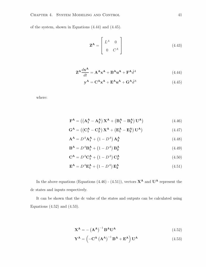
Chapter 4. System Modeling and Control 41
of the system, shown in Equations (4.44) and (4.45).
ZA =
⎡⎢⎣ LA 0
0 CA
⎤⎥⎦ (4.43)
ZAdxA
dt= AAxA + BAuA + FAdA (4.44)
yA = CAxA + EAuA + GAdA (4.45)
where:
FA =((
AA1 −AA
2
)XA +
(BA
1 −BA2
)UA
)(4.46)
GA =((
CA1 −CA
2
)XA +
(EA
1 − EA2
)UA
)(4.47)
AA = DAAA1 +
(1 − DA
)AA
2 (4.48)
BA = DABA1 +
(1 − DA
)BA
2 (4.49)
CA = DACA1 +
(1 − DA
)CA
2 (4.50)
EA = DAEA1 +
(1 − DA
)EA
2 (4.51)
In the above equations (Equations (4.46) - (4.51)), vectors XA and UA represent the
dc states and inputs respectively.
It can be shown that the dc value of the states and outputs can be calculated using
Equations (4.52) and (4.53).
XA = − (AA
)−1BAUA (4.52)
YA =(−CA
(AA
)−1BA + EA
)UA (4.53)

Chapter 4. System Modeling and Control 42
where the dc inputs are defined by:
UA =
⎡⎢⎢⎢⎢⎣
V Ag
V AD
IAo
⎤⎥⎥⎥⎥⎦ . (4.54)
Using Figure 4.8, the state equations for both parts of the switching cycle can be
written. Beginning with the first part of the switching cycle when transistor Q1 is on,
the state and output equations are shown in Equations (4.55) - (4.59).
LA dxA1
dt= uA
1 − xA1
(RA
L + RAQ
)(4.55)
CA dxA2
dt= −uA
3 (4.56)
yA1 = xA
1 (4.57)
yA2 = xA
1 (4.58)
yA3 = xA
2 − uA3 RA
C (4.59)
From these equations, state matrices can be derived, and are shown in Equations
(4.60) - (4.63).

Chapter 4. System Modeling and Control 43
AA1 =
⎡⎢⎣ − (
RAL + RA
Q
)0
0 0
⎤⎥⎦ (4.60)
BA1 =
⎡⎢⎣ 1 0 0
0 0 −1
⎤⎥⎦ (4.61)
CA1 =
⎡⎢⎢⎢⎢⎣
1 0
1 0
0 1
⎤⎥⎥⎥⎥⎦ (4.62)
EA1 =
⎡⎢⎢⎢⎢⎣
0 0 0
0 0 0
0 0 −RAC
⎤⎥⎥⎥⎥⎦ (4.63)
For the second part of the switching cycle diode D1 conducts and the state and output
equations are shown in Equations (4.64) - (4.68).
LA dxA1
dt=
−1
n
(uA
2 +(
xA1
n− uA
3
)RA
C + xA2 +
xA1 RA
s
n
)− RA
LxA1 (4.64)
CAdxA
2
dt=
xA1
n− uA
3 (4.65)
yA1 = xA
1 (4.66)
yA2 = 0 (4.67)
yA3 = xA
2 +
(xA
1
n− uA
3
)RA
C (4.68)
The state matrices for the second part of the switching cycle can be written:

Chapter 4. System Modeling and Control 44
AA2 =
⎡⎢⎣
(−1n2
(RA
C + RAs
) − RAL
) −1n
1n
0
⎤⎥⎦ (4.69)
BA2 =
⎡⎢⎣ 0 −1
n
RAC
n2
0 0 −1
⎤⎥⎦ (4.70)
CA2 =
⎡⎢⎢⎢⎢⎣
1 0
0 0
RAC
n1
⎤⎥⎥⎥⎥⎦ (4.71)
EA2 =
⎡⎢⎢⎢⎢⎣
0 0 0
0 0 0
0 0 −RAC
⎤⎥⎥⎥⎥⎦ (4.72)
Using Equations (4.60) - (4.63) and (4.69) - (4.72), the matrices required for the ac
state space model of Equations (4.44) and (4.45) are found and shown in Equations (4.73)
- (4.78).

Chapter 4. System Modeling and Control 45
AA =
⎡⎢⎣ DA
(−RAL − RA
Q
)+
(1 − DA
) (−1n2
(RA
C + RAs
) − RAL
) −(1 − DA)/n
(1−DA)n
0
⎤⎥⎦ (4.73)
BA =
⎡⎢⎣ DA −(1−DA)
n
(1−DA)RAC
n2
0 0 −1
⎤⎥⎦ (4.74)
FA =
⎡⎢⎣
−(DAV Ag +IA
o RALn+nIA
o RAQ−V A
g )(−1+DA)2
1(−1+DA)IA
o
⎤⎥⎦ (4.75)
CA =
⎡⎢⎢⎢⎢⎣
1 0
DA 0
RAC
(1 − DA
)1
⎤⎥⎥⎥⎥⎦ (4.76)
EA =
⎡⎢⎢⎢⎢⎣
0 0 0
0 0 0
0 0 RAC
⎤⎥⎥⎥⎥⎦ (4.77)
GA =
⎡⎢⎢⎢⎢⎣
0
−n(−1+DA)IA
o
RACnIA
o
(−1+DA)
⎤⎥⎥⎥⎥⎦ (4.78)
4.2.3 Additional parts of the system model
In addition to state space models of the converters, transfer functions must be defined
to complete the system model. They are described below.
4.2.3.1 Additional gain in current loop
Since the flyback current controller will be acting as a PFC in this system, it must track
the input current. From the ideal large signal model of the flyback converter, the input
current and inductor current are related as shown in Equation (3.18), repeated below for

Chapter 4. System Modeling and Control 46
convenience:
⟨iAg (t)
⟩Ts
= d (t)⟨iAL (t)
⟩Ts
(4.79)
However, in the proposed system, the inductor current will be measured on the sec-
ondary side. Thus an additional factor of n from the turns ratio of the transformer must
also be added, resulting in Equation (4.80).
⟨iAg (t)
⟩Ts
= nd (t)⟨iAL (t)
⟩Ts
(4.80)
This gain will be incorporated into the loop gain of the current controller to deduce the
input current from the measured current. It is important to include this value (instead
of absorbing it into the controller) because while the converter is operating as a PFC,
the duty cycle will be varying considerably as shown in Section 3.2.3.
4.2.3.2 Additional components used in digital control
As stated in Section 2.4, digital techniques will be used to implement the controller.
Therefore, a digital pulse-width modulator (DPWM) block and an analog to digital
converter (ADC) block must be modeled in continuous time. Both of these models can
be found in [23], and are repeated below:
Gdpwm (s) =1
Ldpwme−sTdpwm (4.81)
Gadc (s) =
(1 − 2−nadc
Vmaxadc
)e−sTadc (4.82)
where Lpwm is the number of discrete steps in the DPWM, Tpwm is the period of the
DPWM, nadc is the number of bits of the ADC , Vmaxadcis the maximum input voltage
into the ADC and Tadc is the update period of the ADC.

Chapter 4. System Modeling and Control 47
However, since the dynamics of the system that we are interested in are much slower
than the switching period, the analog to digital converter and the digital pulse width
modulator will be approximated with gains as shown in Equations (4.83) and (4.84).
Gdpwm (s) ≈ 1
Ldpwm
= Kdpwm (4.83)
Gadc (s) ≈ 1 − 2−nadc
Vmaxadc
= Kadc (4.84)
4.2.3.3 Digital filter
To control the midpoint voltage of the converter, DMC control is implemented. However,
before the duty cycle of the buck converter can be fed into the voltage loop of the flyback
converter, it must be filtered. This is because a large ripple will appear on the duty cycle
as a consequence from the large ripple voltage on the midpoint capacitor. The filter
is implemented digitally as an eight point moving average filter, operating at 480Hz.
However, in continuous time it will be modeled as a second order filter for simplicity, as
shown in Equation (4.85).
Gf (s) =1
1 +Qf s
ωf+ s2
ω2f
, ωf = 2π30, Qf = 1 (4.85)
4.2.3.4 State space representation of controller
In order to combine the flyback and buck converter models to find an open loop transfer
function that can be used to design the DMC controller, the voltage and current con-
trollers of the buck and flyback converters are represented in state space to simplify the
integration process. The general form of a PI controller in state space is shown in Figure
4.9.
From this figure the state matrices can be found and are described in Equations (4.86)
- (4.88).

Chapter 4. System Modeling and Control 48
p
is1
Figure 4.9: A PI controller in state space.
API = [0] (4.86)
BPI = [1] (4.87)
CPI = [Ki] (4.88)
EPI = [Kp] (4.89)
4.2.4 Complete system model in state space
Using the models built in Sections 4.2.1, 4.2.2 and 4.2.3, the complete small signal system
model can be built, and it is shown in Figure 4.10.
ZAxA = AAxA + BAuA + FAdyA = CAxA + DAuA + GAd
Flyback ConverterxB = ABxB + BBuB
yB = CBxB + DBuB
Buck Converter
GvB(s)
GvA(s)Gi
A(s)
Agv
DBref
VBref
VgA
u1A
u3A
u1B
u2B
y3A
y1A
y1B
y2B
Kadc2
Kadc1
Kadc3
KdpwmA Kdpwm
B
Gf(s)
nDA
dA
kA dB
Figure 4.10: The complete small signal model of the system.
In order to be able to design a controller for DMC controller, the control to output
transfer function must be extracted from the model of Figure 4.10. To obtain this transfer
function, the ASYS, BSYS, CSYS and ESYS state matrices of the system are derived.

Chapter 4. System Modeling and Control 49
This uses the state space models of the lossy buck, lossy flyback and controllers already
created. Using Equation (4.31), the transfer function from input kA to output dB (as
shown on Figure 4.10) can be extracted. Multiplying this by the filter, Gf (s), yields the
control to output transfer function sought.
To find the system state space matrices, the voltage controller of the buck converter
and the current controller of the flyback converter are replaced with PI controllers, defined
by state Equations (4.90), (4.91) and (4.92), (4.93), respectively.
xBPI = uB
PI (4.90)
yBPI = KB
i xBPI + KB
p uBPI (4.91)
xAPI = uA
PI (4.92)
yAPI = KA
i xAPI + KA
p uAPI (4.93)
To combine all the models derived in previous sections, an augmented system with
superscripts ·TOT is created and defined in Equations (4.94) and (4.95).
xTOT = ATOTxTOT + BTOTuTOT (4.94)
yTOT = CTOTxTOT + ETOTuTOT (4.95)
The states, inputs and outputs are defined by Equations (4.96) - (4.98).

Chapter 4. System Modeling and Control 50
xTOT =
⎡⎢⎢⎢⎢⎢⎢⎢⎣
xA
xAPI
xB
xBPI
⎤⎥⎥⎥⎥⎥⎥⎥⎦
(4.96)
uTOT =
⎡⎢⎢⎢⎢⎢⎢⎢⎢⎢⎢⎢⎣
uA
dA
uAPI
uB
uAPI
⎤⎥⎥⎥⎥⎥⎥⎥⎥⎥⎥⎥⎦
(4.97)
yTOT =
⎡⎢⎢⎢⎢⎢⎢⎢⎣
yA
yAPI
yB
yBPI
⎤⎥⎥⎥⎥⎥⎥⎥⎦
(4.98)
The total state matrices are defined by Equations (4.99) - (4.102).

Chapter 4. System Modeling and Control 51
ATOT =
⎡⎢⎢⎢⎢⎢⎢⎢⎣
(ZA
)−1AA 0 0 0
0 AAPI 0 0
0 0 AB 0
0 0 0 ABPI
⎤⎥⎥⎥⎥⎥⎥⎥⎦
(4.99)
BTOT =
⎡⎢⎢⎢⎢⎢⎢⎢⎣
(ZA
)−1BA
(ZA
)−1FA 0 0 0
0 0 BAPI 0 0
0 0 0 BB 0
0 0 0 0 BBPI
⎤⎥⎥⎥⎥⎥⎥⎥⎦
(4.100)
CTOT =
⎡⎢⎢⎢⎢⎢⎢⎢⎣
CA 0 0 0
0 CAPI 0 0
0 0 CB 0
0 0 0 CBPI
⎤⎥⎥⎥⎥⎥⎥⎥⎦
(4.101)
ETOT =
⎡⎢⎢⎢⎢⎢⎢⎢⎣
EA GA 0 0 0
0 0 EAPI 0 0
0 0 0 EB 0
0 0 0 0 EBPI
⎤⎥⎥⎥⎥⎥⎥⎥⎦
(4.102)
The system model will have the same states as the augmented model, and for sim-
plicity the outputs will also be the same, as given in Equations (4.103) and (4.104).
xTOT = xSYS (4.103)
yTOT = ySYS (4.104)
However, the inputs into the system model will be different and are defined in Equa-
tion (4.105).

Chapter 4. System Modeling and Control 52
uSYS =
⎡⎢⎢⎢⎢⎣
uSY S1
uSY S2
uSY S3
⎤⎥⎥⎥⎥⎦ =
⎡⎢⎢⎢⎢⎣
uA1
uA2
kA
⎤⎥⎥⎥⎥⎦ =
⎡⎢⎢⎢⎢⎣
vAg
vAD
kA
⎤⎥⎥⎥⎥⎦ (4.105)
Using Figure 4.10, interconnection of the systems is described by Equations (4.106).
uTOT = NyTOT + MuSYS (4.106)
where,
N =
⎡⎢⎢⎢⎢⎢⎢⎢⎢⎢⎢⎢⎢⎢⎢⎢⎢⎢⎢⎢⎢⎢⎣
0 0 0 0 0 0 0
0 0 0 0 0 0 0
0 0 0 0 0 1 0
0 0 0 KApwm 0 0 0
−nDAKadc1 0 0 0 0 0 0
0 0 1 0 0 0 0
0 0 0 0 0 0 KBpwm
0 0 0 0 −Kadc3 0 0
⎤⎥⎥⎥⎥⎥⎥⎥⎥⎥⎥⎥⎥⎥⎥⎥⎥⎥⎥⎥⎥⎥⎦
(4.107)
M =
⎡⎢⎢⎢⎢⎢⎢⎢⎢⎢⎢⎢⎢⎢⎢⎢⎢⎢⎢⎢⎢⎢⎣
1 0 0
0 1 0
0 0 0
0 0 0
0 0 1
0 0 0
0 0 0
0 0 0
⎤⎥⎥⎥⎥⎥⎥⎥⎥⎥⎥⎥⎥⎥⎥⎥⎥⎥⎥⎥⎥⎥⎦
(4.108)

Chapter 4. System Modeling and Control 53
Substituting Equations (4.103), (4.104) and (4.106) into Equations (4.96) and (4.98)
yields:
xSYS = ATOTxSYS + BTOT(NySYS + MuSYS
)(4.109)
ySYS = CTOTxSYS + ETOT(NySYS + MuSYS
)(4.110)
Solving for ySY S yields Equations (4.111).
ySYS =(I − ETOTN
)−1CTOTxSYS +
(I7×7 −ETOTN
)−1ETOTMuSYS (4.111)
where I is the 7 × 7 identity matrix. Substituting equation(4.111) into Equation
(4.109) and rearranging yields Equation (4.112).
xSYS =(ATOT + BTOTN
(I7×7 − ETOTN
)−1CTOT
)xSYS
+(BTOTM + BTOTN
(I7×7 −ETOTN
)−1ETOTM
)uSYS (4.112)
From Equations (4.111) and (4.112), the state matrices of the system are found and
are shown in Equations (4.113) - (4.116).
ASYS =(ATOT + BTOTN
(I7×7 −ETOTN
)−1CTOT
)(4.113)
BSYS =(BTOTM + BTOTN
(I7×7 − ETOTN
)−1ETOTM
)(4.114)
CSYS =(I7×7 −ETOTN
)−1CTOT (4.115)
ESYS =(I7×7 −ETOTN
)−1ETOTM (4.116)

Chapter 4. System Modeling and Control 54
Using these state matrices, the control to output transfer function can be found.
4.3 Controller design
This section goes through the analysis and controller design of the proposed system as
shown in Figure 2.3. There are three controllers to design: a voltage controller for the
downstream buck converter, a voltage controller for the flyback which will utilize DMC
and a current controller for the flyback.
4.3.1 Voltage controller design for buck converter
Using parameters from the converter designed in the laboratory, a controller will be
designed for the buck converter. The control to output transfer function can be found
by using Equation (4.31), and is shown in Equation (4.117).
GBvc (s) =
vB
dB=
V Bg
1 +(RB
Q+RBL)
RB + s(
LB
RB + RBQCB + RB
L CB)
+ s2CBLB
(4.117)
Table 4.2 lists all the parameters of the buck converter and appropriate ADC and
DPWM. The bode plot of the system can be obtained by substituting these parameters
into Equation (4.117) and multiplying by the transfer functions of the DPWM and ADC,
yielding Figure 4.11.
For this converter, a proportional integral (PI) controller was designed. The zero
was chosen to be as close to the natural frequency of the buck converter as possible
to maximize the bandwidth, while maintaining a large phase margin for all operating
conditions. This zero was placed at 10.98kHz .
The gain was adjusted to provide a large phase margin for all operating conditions.
Figure 4.12 shows the compensated loop gain of the buck converter at the operating point

Chapter 4. System Modeling and Control 55
Table 4.2: Parameters used in the buck converter developed in lab.Parameter Value Units
CB 47.00 μFLB 4.70 μHDB 0.20 - 0.41V B
g 30.00 - 60.00 VV B 12.00 VRB
Q 0.25 ΩRB
L 9.50 mΩRB 7.20 - 14.40 Ω
LBdpwm 252
TBdpwm 1.26 μs
Kadc3 1.24
101
102
103
104
105
−70
−60
−50
−40
−30
−20
Frequency (Hz)
Mag
nitu
de (
dB)
Magnitude
101
102
103
104
105
−180
−90
0
Frequency (Hz)
Pha
se (
deg)
Phase
Figure 4.11: The bode plot of the uncompensated[Bode plot of GAic (s)] control to output
transfer function of the buck converter, GBvc (s).
with the worst phase margin. Its phase margin can be calculated to be 81.4◦ .
Knowing this, the designed controller can be implemented digitally. To do this, the
bilinear transform [33] was used to transform the controller from continuous time to
discrete time. The result is shown in Equation (4.118).

Chapter 4. System Modeling and Control 56
101
102
103
104
105
−60
−40
−20
0
20
40
60
Frequency (Hz)M
agni
tude
(dB
)
Magnitude
101
102
103
104
105
−180
−90
Frequency (Hz)
Pha
se (
deg)
Phase
Figure 4.12: The bode plot of the compensated control to output transfer function of thebuck converter, GB
vc (s), under the operating condition with the smallest phase margin.
d [n] = 12e [n] − 11 [n] + d [n] (4.118)
4.3.2 Current controller design for the flyback converter
In this section, a controller is designed for the current controller of the flyback converter.
The design is based on parameters of the actual prototype designed in the lab. To
determine the control to output transfer function, convert Equation (4.44) to the Laplace
domain, solve for the states x, substitute the result into equation(4.45), set all other
inputs to zero and solve for y (s) /d (s). The result is shown below:
Gid (s) =iAL
dA=
[1 0 0
](CA
(KAs −AA
)−1FA + GA
)(4.119)
Using the matrices found in Section 4.2.2, the transfer function is found and is shown
in Equation (4.120).

Chapter 4. System Modeling and Control 57
Gid (s) = GAd0
sωA
z+ 1
aAs2 + bAs + 1(4.120)
where,
GAd0 =
nIAo
(1 − DA)2(4.121)
ωAz =
IAo
(1 − DA
)2
nCAIAo
(−RAQ − RA
L
)+ CAV A
g (1 − DA)(4.122)
aA =n2CALA
(1 − DA)2(4.123)
bA =n2CA
(RA
L + DARAQ
)+ CA
(1 − DA
) (RA
C + RAs
)(1 − DA)2 (4.124)
Table 4.3 lists all the parameters of the flyback converter developed in the laboratory
that were substituted into Equation (4.120). Figure 4.13 shows the bode plot of the
uncompensated control to output transfer function.
Table 4.3: Parameters used in the flyback converter developed in lab.Parameter Value Units
CA1 150.00 μF
LA 0.70 μHDA 0.34 - 0.61V A
g 85.00 - 225.00 VRMS
V A 50.00 VRA
Q 2.70 ΩRA
L 0.51 ΩRA
s 1.00 ΩRA
C 0.10 ΩIAo 0.50 - 2.00 An 0.32
V AD 1.50 V
LAdpwm 500
TAdpwm 2.50 μs
Kadc1 446.82

Chapter 4. System Modeling and Control 58
101
102
103
104
105
−80
−70
−60
−50
−40
−30
Frequency (Hz)M
agni
tude
(dB
)
Magnitude
101
102
103
104
105
−4
−3
−2
−1
0
1
2
Frequency (Hz)
Pha
se (
deg)
Phase
Figure 4.13: The bode plot of the uncompensated control to output transfer function ofthe flyback converter.
For this system, a PI controller was designed. The zero of the controller was chosen to
be placed after the zero of the plant which causes the gain to decrease at low frequencies.
Therefore, the zero of the controller was placed at 18.19kHz . This results in a constant
gain at low frequencies in the compensated system which gradually tapers off, as shown
in Figure 4.14.
The designed controller can be implemented digitally using the bilinear transform [33].
The result is shown in Equation (4.125).
d [n] = 16e [n] − 12e [n − 1] + d [n] (4.125)
4.3.3 DMC controller design for the flyback converter
In this section, a controller is designed to execute DMC control to regulate the average
duty cycle of the buck converter. It is based on parameters used in laboratory, as shown
in Tables 4.2, 4.3 and 4.4 and the controllers designed in Sections 4.3.1 and 4.3.2. The

Chapter 4. System Modeling and Control 59
101
102
103
104
105
−40
−20
0
20
40
60
Frequency (Hz)M
agni
tude
(dB
)
Magnitude
101
102
103
104
105
−90
−45
0
Frequency (Hz)
Pha
se (
deg)
Phase
Figure 4.14: The bode plot of the compensated control to output transfer function of theflyback converter.
control to output transfer function is derived using the state matrices derived in Equations
(4.113) to (4.116). Additionally, the transfer function derived is then multiplied by the
transfer function used to estimate the low pass filter as defined by Equation (4.85). The
resulting control to output transfer function for DMC control is shown in Figure 4.15.
Table 4.4: Parameters from the laboratory used in the complete system model.Parameter Value Units
Kadc2 13.86
As shown in the figure, the system exhibits a −180◦ phase shift at dc. This is correct
because the output of this transfer function is a duty cycle of a constant power converter.
Hence, when the duty cycle of the flyback converter increases, the mid point voltage will
increase, and then the duty cycle of the buck converter will decrease.
This transfer function is dominated by the slow filter used to filter out the ripple duty
cycle on the downstream buck converter. Therefore a slow PI controller was designed
with a corner frequency of 3.09Hz . The compensated system is shown in Figure 4.16.

Chapter 4. System Modeling and Control 60
10−1
100
101
102
103
104
−100
−50
0
50
100
Frequency (Hz)M
agni
tude
(dB
)
Magnitude
10−1
100
101
102
103
104
−270
−180
Frequency (Hz)
Pha
se (
deg)
Phase
Figure 4.15: The bode plot of the uncompensated control to output transfer function ofthe system using DMC control.
Note that the system appears to have a negative phase margin, and should be unstable.
However, the system is indeed stable. This negative phase margin can be attributed to
the DMC architecture of the system, which should be studied more rigorously in future
work.
The designed controller can be implemented digitally using the bilinear transform [33].
This particular controller does not execute every switching cycle. It executes every time
the digital filter is updated, which occurs at a frequency of 480Hz. The result is shown
in Equation (4.126).
d [n] = 150e [n] − 147e [n − 1] + d [n] (4.126)

Chapter 4. System Modeling and Control 61
10−1
100
101
102
103
104
−50
0
50
100
150
200
Frequency (Hz)
Mag
nitu
de (
dB)
Magnitude
10−1
100
101
102
103
104
−270
−180
Frequency (Hz)
Pha
se (
deg)
Phase
Figure 4.16: The bode plot of the compensated control to output transfer function of thesystem using DMC control.

Chapter 5
Experimental Results
This chapter presents the results obtained with an experimental prototype of the ac/dc
system described in the previous chapters. The prototype was fully fabricated in the
laboratory with off-shelf discrete components for the power stages and an FPGA devel-
opment board to implement the controller. First, some discussion is presented on the
component selections made for the flyback converter. This is because the main storage
capacitor will have a large ripple voltage and it must be properly designed. Following
this, performance results from steady state and transient tests are presented. Finally this
chapter will conclude with advantages and limitations of the designed system.
5.1 Flyback component selection
5.1.1 Flyback transformer
The flyback transformer was chosen in order to meet the following criteria:
• The primary coil can be excited with a rectified, universal ac input voltage of
85 − 265VRMS.
• The turns ratio of no more than 1 : 0.5 to step down the voltage.
62

Chapter 5. Experimental Results 63
• A power rating of at least 40W .
• Readily available for purchase.
Using this criteria, the flyback transformer chosen was model number Z9260-AL man-
ufactured by CoilcraftR©.
5.1.2 Main energy storage capacitor
The main energy storage capacitor is also the output capacitor of the flyback converter.
Since this capacitor has a large ripple voltage on it, it must be designed in accordance
with Equation (3.12). The technical specifications of this capacitor for one phase of the
converter are shown in Table 5.1.
Table 5.1: Technical specifications for the main energy storage capacitor.Parameter Value Units
Pout 20 WηBuck 80 %
Vnominal 50 VΔVMAX 15 V
Using these specifications, an electrolytic 100μF capacitor was chosen manufactured
by PanasonicR©, model number: EEUFC1J101L. Its specifications are shown in Table 5.2,
and they can be substituted into Equation (3.12). The result of the power it can provide
is shown in Equation (5.1), and is well within the design criteria of Table 5.1 with a
factor of safety of 2.2.
Table 5.2: Technical specifications of the main energy storage capacitor chosen,PanasonicR© EEUFC1J101.
Parameter Value Units
Iripple at 120Hz 823 mAVMAX 63 VRESR 0.230 Ω
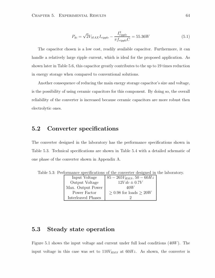
Chapter 5. Experimental Results 64
Pdc =√
2VMAXIripple −I2ripple
πfrippleC= 55.36W (5.1)
The capacitor chosen is a low cost, readily available capacitor. Furthermore, it can
handle a relatively large ripple current, which is ideal for the proposed application. As
shown later in Table 5.6, this capacitor greatly contributes to the up to 19 times reduction
in energy storage when compared to conventional solutions.
Another consequence of reducing the main energy storage capacitor’s size and voltage,
is the possibility of using ceramic capacitors for this component. By doing so, the overall
reliability of the converter is increased because ceramic capacitors are more robust then
electrolytic ones.
5.2 Converter specifications
The converter designed in the laboratory has the performance specifications shown in
Table 5.3. Technical specifications are shown in Table 5.4 with a detailed schematic of
one phase of the converter shown in Appendix A.
Table 5.3: Performance specifications of the converter designed in the laboratory.Input Voltage 85 − 265VRMS, 50 − 60Hz
Output Voltage 12V dc ± 0.7VMax. Output Power 40W
Power Factor ≥ 0.98 for loads ≥ 20WInterleaved Phases 2
5.3 Steady state operation
Figure 5.1 shows the input voltage and current under full load conditions (40W ). The
input voltage in this case was set to 110VRMS at 60Hz. As shown, the converter is

Chapter 5. Experimental Results 65
Table 5.4: Technical specifications of each phase of the converter designed in the labora-tory. Note that capacitor CA is the main energy storage component of the system.
Flyback ConverterParameter Value Units
LA 0.7 mHCA 150 μF
V Anominal 50 Vfsw 400 kHz
Buck ConverterParameter Value Units
LB 4.7 μHCB 47 μFfsw 800 kHz
operating with excellent power factor correction and in this particular case, the power
factor is 0.99. The total harmonic distortion is 7.4% .
Vg
Ig
Figure 5.1: The input voltage and current of the converter under full load. Vg = 110VRMS,60Hz. From top to bottom: V g line voltage on CH3 at 100V/Div and Ig line currenton CH2 at 1A/Div. Time scale: 10ms/Div
Figure 5.2 shows the voltage on the energy storage capacitor, the output voltage and
the duty cycle of the flyback converter for the same load and input voltage conditions as
in Figure 5.1. In this figure, the large ripple voltage on the capacitor is clearly visible

Chapter 5. Experimental Results 66
at twice the line frequency. It has a peak to peak voltage of 13.98V , or 31.4% as a
percentage of the nominal value. Table 5.5 shows the percentage ripple voltage that is
obtained at half and full loads for input line frequencies of 50Hz and 60Hz. The output
voltage also exhibits some ripple, due to the well known problem of a limited resolution
of the DPWM for the buck converter. There are many solutions to this problem, for
example, a sigma delta DPWM as shown in [34], however this is not a focus of this work.
Finally, the duty cycle of the flyback converter shown in Figure 5.2 exhibits the behaviour
expected by the theoretical duty cycle from Equation (3.29). To obtain this waveform,
the duty cycle signal was connected to an RC filter. Figure 5.3(a) shows the theoretical
and experimental duty cycles on the same axes and Figure 5.3(b) shows the FFT of
both the theoretical and experimental duty cycles without a dc component, normalized
to their fundamental frequency of 120Hz. From these figures, it can be seen that the
experimental duty cycle closely matches the theoretical duty cycle at low frequencies,
and begins to loose this similarity at high frequencies, in the kHz range. This is due to
the fact that the experimental duty cycle is purposefully limited as a safety precaution
and will be discussed further in Section 5.7.
Vm
Vo
Flyback Duty
Figure 5.2: From top to bottom: V m the voltage on the energy storage capacitor onCH2 at 10V/Div, V o the output voltage on CH3 at 10V/Div and the duty cycle of theflyback converter on CH4 at 500mV/Div. Time scale: 5ms/Div

Chapter 5. Experimental Results 67
Table 5.5: The percentage voltage ripple on the main energy storage capacitor at differentloads and line frequencies.
50Hz 60Hz20W 23.19% 19.23%40W 37.06% 31.44%
−0.02 −0.015 −0.01 −0.005 0 0.005 0.01 0.015 0.02 0.0250.4
0.5
0.6
0.7
0.8
0.9
1
Dut
y
Time
ExperimentalTheoretical
(a) The theoretical and experimental duty cycle ofthe flyback converter plotted together.
100
101
102
103
−60
−50
−40
−30
−20
−10
0
Frequency (Hz)
Nor
mal
ized
Mag
nitu
de (
dB)
ExperimentalTheoretical
(b) The FFT of the theoretical and experimentalduty cycles without dc and normalized to 120Hz.
Figure 5.3: Comparing the theoretical and experimental duty cycles.
5.4 Power factor and THD
This section summarizes the performance of the converter as a power factor regulator
and evaluates it on two criteria: the power factor as measured by the power supply used
and the total harmonic distortion as calculated from the input current measured by the
oscilloscope. The details of both instruments can be found in Appendix B.
Figures 5.4(a) and 5.4(b) show the measured power factor. As shown, the converter
maintains a power factor of 0.98 or more for all input voltages under full and half load.
The power factor decreases at high voltages due to the limitations on measuring small
currents which will be discussed in Section 5.7.
Figures 5.5(a) and 5.5(b) show the calculated total harmonic distortion from the
converter developed in the laboratory for all input voltages under full and half load. In
a similar manner and reason that the power factor decreases at high voltages, the THD

Chapter 5. Experimental Results 68
80 100 120 140 160 180 200 220 240 260 2800.95
0.955
0.96
0.965
0.97
0.975
0.98
0.985
0.99
0.995
1
Input Voltage (VRMS
)
Pow
er F
acto
r
20W Load40W Load
(a) fline = 50Hz
80 100 120 140 160 180 200 220 240 260 2800.95
0.955
0.96
0.965
0.97
0.975
0.98
0.985
0.99
0.995
1
Input Voltage (VRMS
)
Pow
er F
acto
r
20W Load40W Load
(b) fline = 60Hz
Figure 5.4: The measured power factor of the converter developed in the laboratory.
increases, as shown in the figures.
80 100 120 140 160 180 200 220 240 260 280
6
8
10
12
14
16
18
20
Input Voltage (V)
Tot
al H
arm
onic
Dis
tort
ion
(%)
20W Load40W Load
(a) fline = 50Hz
80 100 120 140 160 180 200 220 240 260 2806
8
10
12
14
16
18
20
Input Voltage (V)
Tot
al H
arm
onic
Dis
tort
ion
(%)
20W Load40W Load
(b) fline = 60Hz
Figure 5.5: The calculated total harmonic distortion of the converter developed in thelaboratory.
Figure 5.6 shows the worst case odd harmonic content over all loads, input frequen-
cies and voltages plotted against the harmonic current emission limits provided by the
IEC61000-3-2 standard. As shown, the converter developed in the laboratory emitted
at most half the harmonic current limit as provided by this standard, this minimum
occurring at the 9th harmonic current. This also shows that a low cost, PFC supply
can be built with sensing on the secondary side that exceeds any input harmonic current

Chapter 5. Experimental Results 69
standards currently enforced.
0 5 10 15 20 25 30 35 4010
−5
10−4
10−3
10−2
Harmonic Number
Har
mon
ic C
urre
nt m
A/W
IEC61000−3−2 LimitsProposed
Figure 5.6: Harmonic current emissions from the converter built in the laboratory plottedagainst the maximum allowable harmonic current emission as stated in the IEC61000-3-2standard [4].
5.5 Transient response
The transient response of the converter was tested with an input voltage of 110VRMS
at 60Hz under a 50% load step from 20W to 40W . Figures 5.7(a) and 5.8(a) show the
results. The transient responses were obtained by using a self tuning dead zone controller
[30] and DMC. Without the use of a dead zone controller, the transient responses become
very poor and are shown in Figures 5.7(b) and 5.8(b)
From the figures it is evident that despite the large ripple voltage on the main energy
storage capacitor and the little amount of energy stored on it, digital control enabled the
development of a suitable controller that can successfully maintain the mid-point voltage
of the converter through large transients.

Chapter 5. Experimental Results 70
Vm
Vo
Load Step
(a) with dead zone controller
Vm
Vo
Load Step
(b) without dead zone controller
Figure 5.7: The transient response of the converter developed in the laboratory under a50% load step increase, with and without the dead zone controller. From top to bottom:V m the voltage on the main energy storage capacitor on CH2 at 20V/Div, V o the outputvoltage on CH3 at 10V/Div and the load step signal on CH4 at 20V/Div. Time scale:20ms/Div
Vm
Vo
Load Step
(a) with dead zone controller
Vm
Vo
Load Step
(b) without dead zone controller
Figure 5.8: The transient response of the converter developed in the laboratory under a50% load step decrease, with and without the dead zone controller. From top to bottom:V m the voltage on the main energy storage capacitor on CH2 at 20V/Div, V o the outputvoltage on CH3 at 10V/Div and the load step signal on CH4 at 20V/Div. Time scale:20ms/Div
5.6 Energy storage comparison
One of the main features of the proposed system is its reduced energy storage. Table 5.6
compares the proposed system to three other PFC supplies supplied by three different
manufacturers.
As shown, the proposed solution has a significant reduction in energy storage from
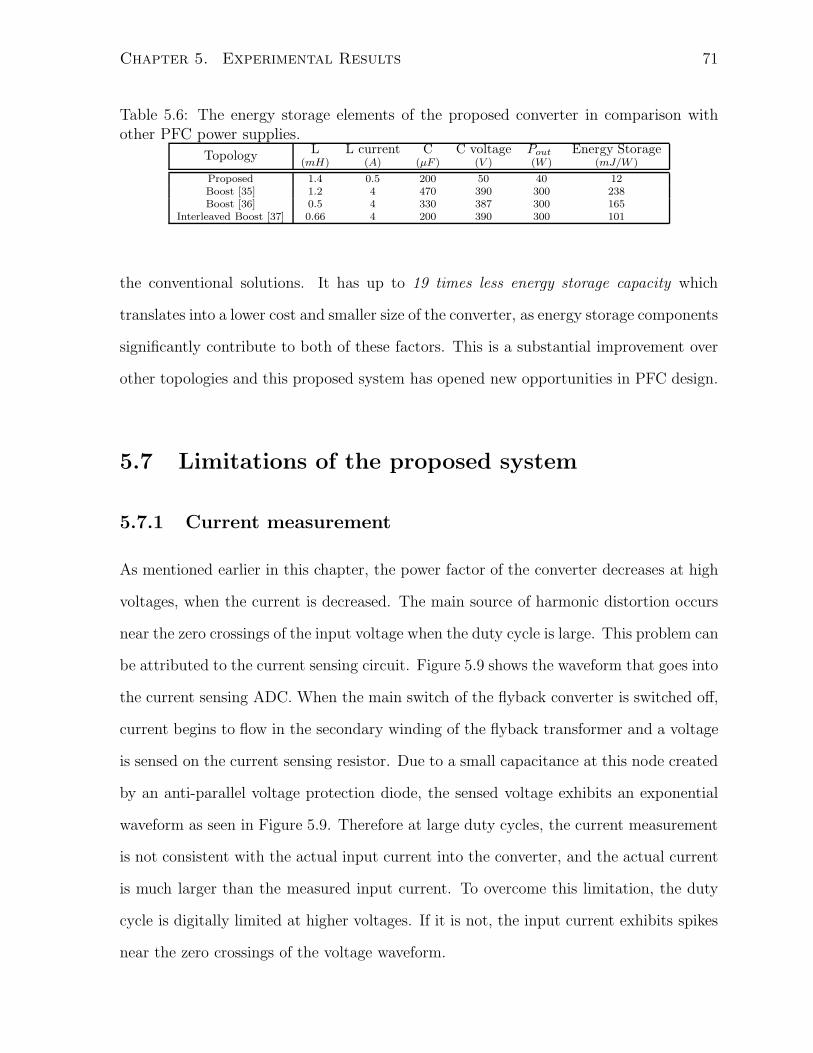
Chapter 5. Experimental Results 71
Table 5.6: The energy storage elements of the proposed converter in comparison withother PFC power supplies.
Topology L L current C C voltage Pout Energy Storage(mH) (A) (μF ) (V ) (W ) (mJ/W )
Proposed 1.4 0.5 200 50 40 12Boost [35] 1.2 4 470 390 300 238Boost [36] 0.5 4 330 387 300 165
Interleaved Boost [37] 0.66 4 200 390 300 101
the conventional solutions. It has up to 19 times less energy storage capacity which
translates into a lower cost and smaller size of the converter, as energy storage components
significantly contribute to both of these factors. This is a substantial improvement over
other topologies and this proposed system has opened new opportunities in PFC design.
5.7 Limitations of the proposed system
5.7.1 Current measurement
As mentioned earlier in this chapter, the power factor of the converter decreases at high
voltages, when the current is decreased. The main source of harmonic distortion occurs
near the zero crossings of the input voltage when the duty cycle is large. This problem can
be attributed to the current sensing circuit. Figure 5.9 shows the waveform that goes into
the current sensing ADC. When the main switch of the flyback converter is switched off,
current begins to flow in the secondary winding of the flyback transformer and a voltage
is sensed on the current sensing resistor. Due to a small capacitance at this node created
by an anti-parallel voltage protection diode, the sensed voltage exhibits an exponential
waveform as seen in Figure 5.9. Therefore at large duty cycles, the current measurement
is not consistent with the actual input current into the converter, and the actual current
is much larger than the measured input current. To overcome this limitation, the duty
cycle is digitally limited at higher voltages. If it is not, the input current exhibits spikes
near the zero crossings of the voltage waveform.

Chapter 5. Experimental Results 72
Duty Cycle
Measured Current
Figure 5.9: Current sensing waveform. From top to bottom: the duty cycle of theflyback converter on CH1 at 2V/Div and the input to the current sensing ADC on CH2at 100mV/Div. Time scale: 2μs/Div
5.7.2 Loss in main energy storage capacitor
A trade off of the proposed converter is energy storage for a large ripple voltage on the
main energy storage capacitor of the system. As a consequence, the ripple current in this
capacitor will generate some losses proportional to the ESR of the capacitor, and this
loss can be calculated using the theoretical capacitor voltage obtained in Equation (3.28).
Taking the derivative of this equation, multiplying by the capacitance and substituting
VgIg/2 for Pdc yields the current in the capacitor, described in Equation (5.2).
ic (t) = −Pdccos (2ωt)√
Pdc sin(2ωt)ωC
+ V 20
(5.2)
Using this equation the power lost in the energy storage capacitor, PC , is determined
by Equation (5.3).
PC =ω
2π
∫ (2π/ω)
0
i2c (t)RESR dt (5.3)
Therefore in the worst case scenario where the average efficiency of the buck converter
is 70%, the power lost in the main energy storage capacitor can be calculated to be

Chapter 5. Experimental Results 73
76.9mW .
This analysis shows that even with a larger ripple current on the main energy storage
capacitor, the losses due to this current are very small compared with the output power
of the converter. This occurs because typical manufactured capacitors exhibit a direct
relationship between energy storage and ESR, as the energy storage decreases, the ESR
also decreases.
5.7.3 Hold up time
Hold up time, also known as ride through time, is a converter’s ability to provide a
continuous output voltage in the event of a temporary fault in the ac voltage. For
manufacturers of dc power supplies for information technology (IT) applications, there is
a standard created by the Information Technology Industry Council which they should
adhere to if the voltage sags, swells or is interrupted for a certain period of time. This
standard is summarized in Figure 5.10, which is commonly known as the CBEMA Curve.
From the figure, the ITIC recommends that a power supply have a hold up time of at
least 20ms, or one line cycle at 50Hz. For the proposed system, the hold up time in the
worst case is about 4ms. Figure 5.11 shows the hold up time of the proposed converter
built in the laboratory under full load conditions with an input voltage of 110VRMS at
50Hz. As shown, the voltage is switched off near zero, and the output voltage is able to
remain constant for only another 4ms after the switch off. However this does not mean
the proposed system is not a viable solution. The proposed solution can be implemented
for devices that do not require such a stringent hold up time, like battery powered devices
such as laptops. The CBEMA Curve was developed to protect sensitive and essential
equipment. Furthermore, battery charging applications is an area of the market where
it is more desirable to have a power supply that is smaller and lighter at the expense of
hold up time because it must be carried around with the device.

Chapter 5. Experimental Results 74
Figure 5.10: The CBEMA Curve [1].

Chapter 5. Experimental Results 75
Vm
Vo
Vg measured
Figure 5.11: Hold up time of the converter developed in the laboratory under full loadconditions with an input voltage of 110VRMS at 50Hz. From top to bottom: V m thevoltage on the main energy storage capacitor on CH2 at 10V/Div, V o the output voltageon CH3 at 10V/Div and the input voltage sensed on the secondary side on CH4 at1V/Div. Time scale: 5ms/Div

Chapter 6
Conclusions and Future Work
This chapter summarizes the results of this work, and proposes future work for consid-
eration.
6.1 Conclusions
This research presented a power factor corrected ac/dc power supply with reduced energy
storage elements. It was shown that the area of low power supplies might soon be
subjected to input harmonic current limitations. As a consequence, small, inexpensive
low power PFC supplies are expected to be in high demand. Furthermore, many low
power ac/dc supplies are used for portable electronics devices such as laptops, and these
devices do not require a power supply to meet the hold up time requirements put forth
by the ITIC. Therefore this work proposes a solution to minimize the energy storage
components of a power supply, allowing a large ripple voltage on the main energy storage
capacitor and a unified digital controller to create a small portable power supply. The
total energy storage in the PFC stage of the converter was shown to be up to 19 times
less than conventional solutions.
The effectiveness of the proposed solution was shown through a prototype developed
in the laboratory and the resulting converter maintained a power factor greater than 0.98
76

Chapter 6. Conclusions and Future Work 77
for all loading and input voltage conditions. Furthermore, all the sensing and control for
the entire converter was implemented on the isolated side of the system. The controller
was implemented digitally with a single FPGA.
A new control method for controlling cascaded converters, DMC, was also proposed
and implemented in the system. This new control method was briefly studied in this
work and through that analysis it was shown that DMC control can improve the transient
response of a system, and is not limited to PFC supplies. DMC can be applied to any
cascade connection of SMPS to decrease the energy storage components of that system.
6.2 Future work
This work has opened up two new areas which can be expanded upon. First, the de-
sign of PFC power supplies with minimized energy storage components, and second the
development of DMC.
6.2.1 PFC supplies with minimized energy storage
This work can be further extended by perfecting the power factor correction and improv-
ing the efficiency of the supply created and studied in the laboratory.
Additionally, a method to control this power supply without a current sensor can also
be pursued. Removing the 1Ω resistor that currently senses the current would not only
make the power supply more efficient, but also make it a more attractive option.
6.2.2 DMC
This work opened up an entirely novel way to control cascaded SMPS through DMC. It
can be used quite effectively to reduce main energy storage capacitors in not only PFC
supplies, but any cascaded configuration. Some areas to investigate are outlined below.

Chapter 6. Conclusions and Future Work 78
6.2.2.1 DMC controller design
DMC relies on the controller of the downstream converter, however how it depends on
this controller is not fully understood. Therefore a rigorous analysis of a system using
DMC could be pursued. Furthermore, design criteria could be derived that would yield
an optimal controller for DMC and the controller for the downstream converter.
6.2.2.2 Dead beat control using DMC
Consider a system with a downstream converter with dead beat control. In this system,
when a load step occurs, the duty cycle will adjust such that it reaches a new operating
point in one switching cycle. The duty cycle of the downstream converter can then also
be read by the upstream converter to adjust its duty cycle within one switching cycle.
This system could potentially have extremely fast response, and the main energy storage
capacitor could be even further reduced in size.
6.2.2.3 DMC with multiple downstream stages
Extending the problem of DMC to a distributed network of downstream converters in-
troduces new challenges for DMC. The problem can be stated as this: how can the duty
cycles of all the downstream converters be combined to create an error signal for the
DMC controller.
6.2.3 On chip integration
Finally, the proposed solution could be implemented entirely on a single integrated circuit
(IC). The chip could combine a controller which allows a large ripple on the main energy
storage capacitor implementing DMC with all of the switching components, creating a
unified, single chip, isolated PFC supply.

Appendices
79

Appendix A
Circuit Schematic
This appendix contains the circuit schematics of the printed circuit board designed and
built in the laboratory. The schematics are for one phase of the power converter. To
create a second power stage, two PCBs were populated and connected together. Section
A.1 contains the schematic diagrams, and section A.2 contains the bill of materials.
A.1 Circuit schematics
The hierarchy of the circuit schematics and corresponding figures are as follows:
• AC/DC PFC supply, Figure A.1
– ADC circuit, Figure A.2
– Linear regulator circuit, Figure A.3
– Non inverting operational amplifier circuit, Figure A.4
– Power stage circuit, Figure A.5
∗ Gate driver circuit, Figure A.6
– Inverting operational amplifier circuit, Figure A.7
80

Appendix A. Circuit Schematic 81
1 1
2 2
3 3
4 4
DD
CC
BB
AA
VA
Crect
Vout+
VD
D
Q1Sig
Q2Sig
Q3Sig
Q4Sig
Isense
iVD
D
PowerStage
PowerStage.SchD
oc
GN
D
Q1Sig
Q2Sig
Q3Sig
Q4Sig
AD
C_clock
AD
C_BIT1
AD
C_BIT2
AD
C_BIT3
AD
C_BIT4
AD
C_BIT5
AD
C_BIT6
AD
C_BIT7
AD
C_BIT8
AD
C_BIT9
AD
C_BIT10
AD
C_BIT11
V_sam
pleA
DC_B
IT12
VA
DC
AD
2A
DC_circuit.SchD
oc
AD
2_bit12A
D2_bit11
AD
2_bit10A
D2_bit9
AD
2_bit8A
D2_bit7
AD
2_bit6A
D2_bit5
AD
2_bit4A
D2_bit3
AD
2_bit2A
D2_bit1
Vout+
+5V
Vout+
+5V
+3.3V
+9V
LR1
LinearRegulators.SchDoc
+5V
+3.3V
+9V
AD
C_clock
AD
C_BIT1
AD
C_BIT2
AD
C_BIT3
AD
C_BIT4
AD
C_BIT5
AD
C_BIT6
AD
C_BIT7
AD
C_BIT8
AD
C_BIT9
AD
C_BIT10
AD
C_BIT11
V_sam
pleA
DC_B
IT12
VA
DC
AD
1A
DC_circuit.SchD
oc
AD
1_bit12A
D1_bit11
AD
1_bit10A
D1_bit9
AD
1_bit8A
D1_bit7
AD
1_bit6A
D1_bit5
AD
1_bit4A
D1_bit3
AD
1_bit2A
D1_bit1
+5V
12
34
56
78
910
1112
1314
1516
1718
1920
2122
2324
2526
2728
2930
3132
3334
3536
3738
3940
P1Header 20X
2
12
34
56
78
910
1112
1314
1516
1718
1920
2122
2324
2526
2728
2930
3132
3334
3536
3738
3940
P2Header 20X
2
GN
D
GN
DG
ND
GN
D
Q1Sig
Q2Sig
Q3Sig
Q4Sig
AD
1_bit1A
D1_bit2
AD
1_bit3A
D1_bit4
AD
1_bit5A
D1_bit6
AD
1_bit7A
D1_bit8
AD
1_bit9A
D1_bit10
AD
1_bit11A
D1_bit12
AD
2_bit1A
D2_bit2
AD
2_bit3A
D2_bit4
AD
2_bit5A
D2_bit6
AD
2_bit7A
D2_bit8
AD
2_bit9A
D2_bit10
AD
2_bit11A
D2_bit12
GN
D
+10V+9V
VA
C
AC
1
2
3
4 DB
1
GB
U6J-BP
+10V
VA
CVA
Crect
VA
Crect
GN
D
Isense
AD
C_clock
AD
C_BIT1
AD
C_BIT2
AD
C_BIT3
AD
C_BIT4
AD
C_BIT5
AD
C_BIT6
AD
C_BIT7
AD
C_BIT8
AD
C_BIT9
AD
C_BIT10
AD
C_BIT11
V_sam
pleA
DC_B
IT12
VA
DC
AD
3A
DC_circuit.SchD
oc
+5V
Isense_2
AD
3_bit1A
D3_bit2
AD
3_bit3A
D3_bit4
AD
3_bit5A
D3_bit6
AD
3_bit7A
D3_bit8
AD
3_bit9A
D3_bit10
AD
3_bit11A
D3_bit12
AD
3_bit1A
D3_bit2
AD
3_bit3A
D3_bit4
AD
3_bit5A
D3_bit6
AD
3_bit7A
D3_bit8
AD
3_bit9A
D3_bit10
AD
3_bit11A
D3_bit12
AD
3_CLK
Vin
Vout
VO
A1
OperationalA
mplifierN
onInverting.SchDoc
Vin
Vout
VO
A2
OperationalA
mplifierInverting.SchD
oc
Vout+_2
Vout+_2
Vac_test_2
Vac_test_2
Vin
Vout
IOA
1O
perationalAm
plifierInverting.SchDoc
IsenseIsense_2
12
Connector
ST1
ScrewTerm
inal
12
Connector
ST2
ScrewTerm
inal
12
Connector
ST3
ScrewTerm
inal
12
Connector
ST4
ScrewTerm
inal
AC
_GN
D
AC_G
ND
GN
D
Vac_test
12
Connector
ST5
ScrewTerm
inal
-5V
GN
D
AD
2_CLKA
D1_CLK
AD
1_CLK
AD
2_CLK
AD
3_CLK
+i10V
12
Connector
ST6
ScrewTerm
inal
12
Connector
ST7
ScrewTerm
inal
iGN
D
iGN
D
+i5V
+i10V
Figure A.1: Overall circuit schematic of the converter built in the laboratory.
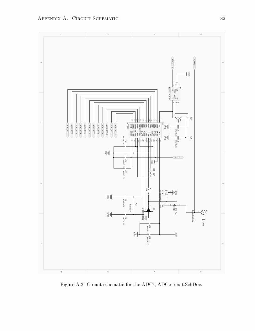
Appendix A. Circuit Schematic 82
1 1
2 2
3 3
4 4
DD
CC
BB
AA
CLK1
BIT12
BIT23
BIT34
BIT45
BIT56
BIT67
BIT78
BIT89
BIT910
BIT1011
BIT1112
BIT1213
OTR
14A
VD
D15
AV
SS16
SENSE
17V
REF
18REFCO
M19
CAPB
20CA
PT21
CML
22V
INA
23V
INB
24A
VSS
25A
VD
D26
DV
SS27
DV
DD
28U
2
AD
9220
GN
D
+3.3V
C610uF/6.3VC710uF/6.3V
C410uF/6.3VC310uF/6.3VG
ND
C810uF/6.3VC910uF/6.3V
C510uF/6.3V
GN
DG
ND
C1010uF/6.3V
R236R
R336R
2 1
3PO
T120K
Pot
GN
D
GN
D
R1200R
+3.3V
C110uF/6.3V
GN
D
+5V
C210uF/6.3V
GN
D
GN
D
AD
C_clock
AD
C_BIT1
AD
C_BIT2
AD
C_BIT3
AD
C_BIT4
AD
C_BIT5
AD
C_BIT6
AD
C_BIT7
AD
C_BIT8
AD
C_BIT9
AD
C_BIT10
AD
C_BIT11
V_sam
ple
AD
C_BIT12
1A1
GN
D2
2A3
2Y4
VC
C5
1Y6
U1
SN74LV
C2G07
VADC
1
2PT3
ProbeTestPoint
1
2
PT4ProbeTestPoint
GN
D
GN
D
12
D1
SKH
00122AED
GN
D
Figure A.2: Circuit schematic for the ADCs, ADC circuit.SchDoc.

Appendix A. Circuit Schematic 83
1 1
2 2
3 3
4 4
DD
CC
BB
AA
GN
D
C2710uF/16V
GN
D
C2810uF/6.3V
GN
D
R10100RD
3SU
PER RED LED
GN
D
GN
DGND2
Output
3V
in1
GND4
U6
LM2937-3.3
GN
DG
ND
R11100RD
2SU
PER RED LED
GN
D
C3010uF/6.3V
C2910uF/16V
+5V
+3.3V
+9V1
2
3ING
ND OU
T
VR
1
L78S05CV
1
2PT1
ProbeTestPoint
1
2PT2
ProbeTestPoint GN
D
GN
D
Figure A.3: Circuit schematic for the linear regulators, LinearRegulator.SchDoc.

Appendix A. Circuit Schematic 84
1 1
2 2
3 3
4 4
DD
CC
BB
AA
+5V
10K
R110K
10K
R210K
GN
D
Vin
Vout
10uF
C310uF/6.3V
GN
D
GN
D
GN
D 10uF
C42.2nF/6.3V 12345 6 7 8
-+V
+
V-
NC
NC
NC
OP1
LM6624
21
3 POT1
20K Pot -5V
Figure A.4: Circuit schematic for the non inverting operational amplifier, Opera-tionalAmplifierNonInverting.SchDoc.
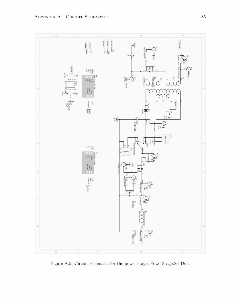
Appendix A. Circuit Schematic 85
1 1
2 2
3 3
4 4
DD
CC
BB
AA
Pri
Sec
Aux
1 3 4 6
78 11 12T1Z92060-A
L1
43
Q1
SPD02N
80C3
1
43
Q3
2SK2503
1
43
Q4
2SK2503
GN
D12
C1EEUFC14151
1 3
2
4 6
5
SW1
S102031MS02Q
GN
D
12
L1DR
1050-2R2-R
12
C2EEUFC1C470
1 R51
VA
Crect
Vout+
Q2Sig
Q3Sig
Q4Sig
VD
DV
DD
LO2
HI2
Source2
LI1
HI1
HO
1
Source1
LO1
VD
DH
OH
ILI
LOSource
Ground
G1
GateD
river.SchDoc
VD
DH
OH
ILI
LOSource
Ground
G2
GateD
river.SchDoc
VD
DiV
DD
HO
1H
O2
HI1
HI2
LI1LI2
LO1
LO2
Source1G
round1G
round2G
ND
Vac_test
Isense
1
2
CP1
Current Probe
1
2
CP2
Current Probe
1
2
CP3
Current Probe
GN
D
+5V+i5V
10uF
C510uF/6.3VLI2
Q1Sig
12345 6 7 8
Opto1
HC
PL-7721-00E
1
2PT5
ProbeTestPoint
1
2PT6
ProbeTestPoint
1
2PT7
ProbeTestPoint
1
2PT8
ProbeTestPoint
1
2
PT9
ProbeTestPoint
GN
D
GN
DG
ND
1
2PT10
ProbeTestPoint
1
2
PT12ProbeTestPoint
1
2PT13
ProbeTestPoint GN
DG
ND
1
2
Connector
ST8
ScrewTerm
inal12
Connector
ST9
ScrewTerm
inal
GN
D
iGN
D
iGN
D
iGN
D
iGN
D
D1
Diode
iGN
DiG
ND
iGN
D
iVD
DiV
DD
1 R61
Figure A.5: Circuit schematic for the power stage, PowerStage.SchDoc.

Appendix A. Circuit Schematic 86
1 1
2 2
3 3
4 4
DD
CC
BB
AA
HO
LO
5 R15/10W5 R25/10W
VD
D
12345 6 7 8
GD
1
UCC27201
10uF
C110uF/20V
10uF
C210uF/25VSource
HI
LI
Ground
C3Cap2
Figure A.6: Circuit schematic of the gate drivers, GateDriver.SchDoc.

Appendix A. Circuit Schematic 87
1 1
2 2
3 3
4 4
DD
CC
BB
AA
+5VG
ND
Vin
Vout
10uF
C110uF/6.3V
GN
D
GN
D
GN
D 10uF
C22.2nF/6.3V1234
5 6 7 8-+
V+
V-
NC
NC
NC
OP1
LM6624
213 PO
T120K
Pot
-5V
21
3
POT2
20K Pot
Figure A.7: Circuit schematic for the inverting operational amplifiers, OperationalAm-plifierInverting.SchDoc.

Appendix A. Circuit Schematic 88
A.2 Bill of materials
Figure A.8 shows the bill of materials for one phase of the power supply. When populating
the second phase of the power supply, only components needed for the power stages were
needed.
Footprint Comment LibRef Designator Description Quantity
EEUFC1H151 EEUFC14151 EEUFC14151 C1 150uF Capacitor 1
C1206 10uF/6.3V Cap Semi C1_AD1, C1_AD2, C1_AD3, C1_IOA1,C1_VOA2, C2_AD1, C2_AD2, C2_AD3,C3, C3_AD1, C3_AD2, C3_AD3, C4_AD1,C4_AD2, C4_AD3, C5, C5_AD1, C5_AD2,C5_AD3, C6_AD1, C6_AD2, C6_AD3,C7_AD1, C7_AD2, C7_AD3, C8_AD1,C8_AD2, C8_AD3, C9_AD1, C9_AD2,C9_AD3, C10_AD1, C10_
Capacitor (Semiconductor SIM Model) 36
C1206 10uF/20V Cap Semi C1_G1, C1_G2 Capacitor (Semiconductor SIM Model) 2EEUFC1C470 EEUFC1C470 EEUFC1C470 C2 47uF Capacitor 1
C1206 10uF/25V Cap Semi C2_G1, C2_G2 Capacitor (Semiconductor SIM Model) 2C1206 2.2nF/6.3V Cap Semi C2_IOA1, C2_VOA2, C4 Capacitor (Semiconductor SIM Model) 3CAPR5-4X5 Cap2 Cap2 C3_G1, C3_G2 Capacitor 2C1206 10uF/16V Cap Semi C27, C29 Capacitor (Semiconductor SIM Model) 2CurrentSensor
Current Probe Current Probe CP1, CP2, CP3 Current Probe, For Agilent 1147A Probe 3
SMC Diode Diode D1 Default Diode 1SOD-123 SKH00122AED SKH00122AED D1_AD1, D1_AD2, D1_AD3 Diode, 200mA, 20V 3SOT23 SUPER RED
LEDSUPER REDLED
D2, D3 Typical RED GaAs LED 2
GBU6J GBU6J-BP GBU6J-BP DB1 Diode Bridge Rectifier, Single Phase 1SOIC127P600-8BN
UCC27201 UCC27201 GD1_G1, GD1_G2 High/Low Side Gate Driver 2
DR1050-2R2-R
DR1050-2R2-R DR1050-2R2-R L1 Inductor 1
SOIC127P600-8AN
LM6624 LM6624 OP1, OP1_IOA1, OP1_VOA2 Operational Amplifier, 1.5Ghz GBP 3
OPTO-DIP8 HCPL-7721-00E HCPL-7721-00E Opto1 Opto Isolator, 25MBPS 1HDR2X20 Header 20X2 Header 20X2 P1, P2 Header, 20-Pin, Dual row 2SM-4W - ext 20K Pot POT25K,
PotentiometerPOT1, POT1_AD1, POT1_AD2,POT1_AD3, POT1_IOA1, POT1_VOA2,POT2_IOA1, POT2_VOA2
Potentiometer 8
TestPoint ProbeTestPoint ProbeTestPoint PT1, PT2, PT3_AD1, PT3_AD2, PT3_AD3,PT4_AD1, PT4_AD2, PT4_AD3, PT5, PT6,PT7, PT8, PT9, PT10, PT12, PT13
Probe Test Point with ground 16
SIP-G3/C6.75 SPD02N80C3 SPD02N80C3 Q1 MOSFET, N-Type 1
SIP-G3/C6.75 2SK2503 2SK2503 Q3, Q4 Transistor, MOSFET, N-Type 2
J1-0603 10K Res3 R1, R2 Resistor 2C1206 200R Res3 R1_AD1, R1_AD2, R1_AD3 Resistor 3AXIAL-0.8 5/10W Res3 R1_G1, R1_G2, R2_G1, R2_G2 Resistor 4C1206 36R Res3 R2_AD1, R2_AD2, R2_AD3, R3_AD1,
R3_AD2, R3_AD3Resistor 6
2012[0805] 1 Res Semi R5 Semiconductor Resistor 1AXIAL-0.3 1 Res1 R6 Resistor 1C1206 100R Res3 R10, R11 Resistor 2ScrewTerminal
ScrewTerminal ScrewTerminal ST1, ST2, ST3, ST4, ST5, ST6, ST7, ST8,ST9
Screw Terminal, 0.2" spacing 9
S102031MS02Q
S102031MS02Q S102031MS02Q SW1 SPST Slide Switch 1
Z9260-AL Z92060-AL Z92060-AL T1 Flyback Transformer 1SC70-6 SN74LVC2G07 SN74LVC2G07 U1_AD1, U1_AD2, U1_AD3 3SOIC28 R-28 AD9220 AD9220 U2_AD1, U2_AD2, U2_AD3 12-bit ADC 10MHz 3SOT-223 LM2937-3.3 LM2937-3.3 U6 Voltage Regulator 1TO-220 L78S05CV L78S05CV VR1 5V Voltage Regulator 2A 1
133
Figure A.8: Bill of materials for one phase of the power stage.
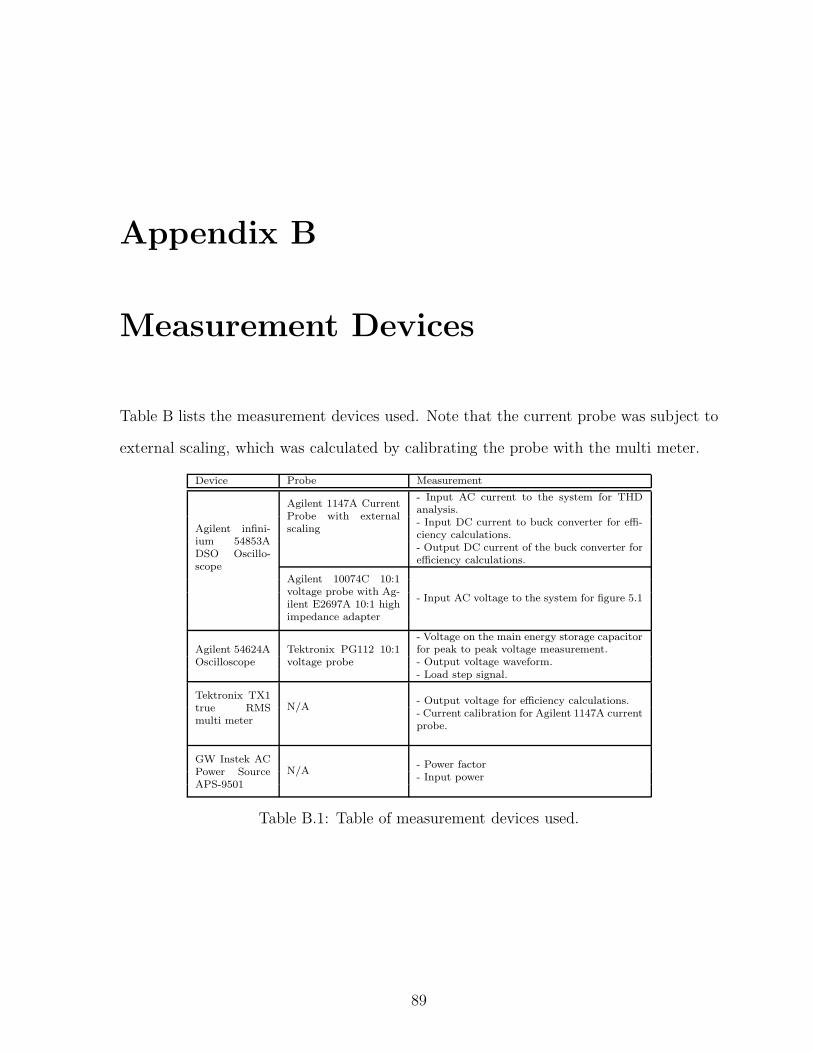
Appendix B
Measurement Devices
Table B lists the measurement devices used. Note that the current probe was subject to
external scaling, which was calculated by calibrating the probe with the multi meter.
Device Probe Measurement
Agilent infini-ium 54853ADSO Oscillo-scope
Agilent 1147A CurrentProbe with externalscaling
- Input AC current to the system for THDanalysis.- Input DC current to buck converter for effi-ciency calculations.- Output DC current of the buck converter forefficiency calculations.
Agilent 10074C 10:1voltage probe with Ag-ilent E2697A 10:1 highimpedance adapter
- Input AC voltage to the system for figure 5.1
Agilent 54624AOscilloscope
Tektronix PG112 10:1voltage probe
- Voltage on the main energy storage capacitorfor peak to peak voltage measurement.- Output voltage waveform.- Load step signal.
Tektronix TX1true RMSmulti meter
N/A- Output voltage for efficiency calculations.- Current calibration for Agilent 1147A currentprobe.
GW Instek ACPower SourceAPS-9501
N/A- Power factor- Input power
Table B.1: Table of measurement devices used.
89

Bibliography
[1] “ITI (CBEMA) curve application note,” Information Technology Industry Council,
2005.
[2] R. W. Erickson and D. Maksimovic, Fundamentals of Power Electronics. Springer
Science+Business Media, LLC, 2001.
[3] “IEEE recommended practices and requirements for harmonic control in electrical
power systems,” IEEE Std 519-1992, Apr 1993.
[4] “Limits for harmonic current emissions (equipment input current less than 16A per
phase),” IEC61000-3-2, 2005.
[5] W. Rynone, “Is power factor correction justified in the home?,” Power Electronics
Technology, pp. 36–39, May 2007.
[6] W. Jewell, “Harmonic limits for single-phase equipment,” Electrical Construction
and Maintenance Magazine, 2002.
[7] Statistics Canada, “2006 census of population,” CANSIM, 2006.
[8] Statistics Canada, “table 203-0020 selected dwelling characteristics and household
equipment,” Income Statistics Division, 2008.
[9] O. Garcia, J. Cobos, R. Prieto, P. Alou, and J. Uceda, “Single phase power factor
correction: a survey,” Power Electronics, IEEE Transactions on, vol. 18, pp. 749–
755, May 2003.
90

Bibliography 91
[10] R. Teodorescu, S. Kjaer, S. Munk-Nielsen, F. Blaabjerg, and J. Pedersen, “Compar-
ative analysis of three interleaved boost power factor corrected topologies in dcm,”
in Power Electronics Specialists Conference, 2001. PESC. 2001 IEEE 32nd Annual,
vol. 1, pp. 3–7, 2001.
[11] A. Lazaro, A. Barrado, J. Pleite, R. Vazquez, and E. Olias, “The series induc-
tance interval, a new family of single-stage pfc converters,” in Industrial Electronics,
2002. ISIE 2002. Proceedings of the 2002 IEEE International Symposium on, vol. 3,
pp. 737–742, 2002.
[12] A. Lazaro, A. Barrado, M. Sanz, V. Salas, and E. Olias, “New power factor correc-
tion ac-dc converter with reduced storage capacitor voltage,” Industrial Electronics,
IEEE Transactions on, vol. 54, pp. 384–397, Feb. 2007.
[13] D. Garinto, “Interleaved boost converter system for unity power factor operation,”
in Power Electronics and Applications, 2007 European Conference on, pp. 1–7, Sept.
2007.
[14] C. Chan and M. Pong, “Interleaved boost power factor corrector operating in
discontinuous-inductor-current mode,” in Power Conversion Conference - Nagaoka
1997., Proceedings of the, vol. 1, pp. 405–410, Aug 1997.
[15] C. Qiao and K. Smedley, “A topology survey of single-stage power factor corrector
with a boost type input-current-shaper,” Power Electronics, IEEE Transactions on,
vol. 16, pp. 360–368, May 2001.
[16] L. Huber, J. Zhang, M. Jovanovi, and F. Lee, “Generalized topologies of single-stage
input-current-shaping circuits,” in Power Electronics Specialists Conference, 2000.
PESC 00. 2000 IEEE 31st Annual, vol. 3, pp. 1336–1341, 2000.
[17] R. Erickson, M. Madigan, and S. Singer, “Design of a simple high-power-factor rec-
tifier based on the flyback converter,” in Applied Power Electronics Conference and

Bibliography 92
Exposition, 1990. APEC ’90, Conference Proceedings 1990., Fifth Annual, pp. 792–
801, Mar 1990.
[18] R. Watson, G. Hua, and F. Lee, “Characterization of an active clamp flyback topol-
ogy for power factor correction applications,” in Applied Power Electronics Confer-
ence and Exposition, 1994. APEC ’94. Conference Proceedings 1994., Ninth Annual,
vol. 1, pp. 412–418, Feb 1994.
[19] S. M. Sandler, “Optimizing single-stage power factor correction,” Power Electronics
Technology, pp. 14–22, March 2006.
[20] N. Papanikolaou and E. Tatakis, “Minimization of power losses in pfc flyback con-
verters operating in the continuous conduction mode,” Electric Power Applications,
IEEE Proceedings -, vol. 149, pp. 283–291, July 2002.
[21] A. Prodic and D. Maksimovic, “Digital pwm controller and current estimator for a
low-power switching converter,” in Computers in Power Electronics, 2000. COM-
PEL 2000. The 7th Workshop on, pp. 123–128, 2000.
[22] S. Choudhury and J. Noon, “A dsp based digitally controlled interleaved pfc con-
verter,” in Applied Power Electronics Conference and Exposition, 2005. APEC 2005.
Twentieth Annual IEEE, vol. 1, pp. 648–654, March 2005.
[23] A. Prodic, D. Maksimovic, and R. Erickson, “Design and implementation of a digital
pwm controller for a high-frequency switching dc-dc power converter,” in Industrial
Electronics Society, 2001. IECON ’01. The 27th Annual Conference of the IEEE,
vol. 2, pp. 893–898, 2001.
[24] V. Rao, A. Jain, K. Reddy, and A. Behal, “Experimental comparison of digital im-
plementations of single-phase pfc controllers,” Industrial Electronics, IEEE Trans-
actions on, vol. 55, pp. 67–78, Jan. 2008.

Bibliography 93
[25] iSuppli, “Notebook pc shipments exceed desktops for the first time in q3,” iSuppli
Corp., December 2008.
[26] S. Abe, M. Hirokawa, and T. Ninomiya, “Output impedance design consideration of
three control schemes for bus converter in on-board distributed power system,” in
Power Electronics and Drive Systems, 2007. PEDS ’07. 7th International Conference
on, pp. 1199–1204, Nov. 2007.
[27] X. Feng, Z. Ye, K. Xing, F. Lee, and D. Borojevic, “Individual load impedance
specification for a stable dc distributed power system,” in Applied Power Electronics
Conference and Exposition, 1999. APEC ’99. Fourteenth Annual, vol. 2, pp. 923–
929, Mar 1999.
[28] C. Wildrick, F. Lee, B. Cho, and B. Choi, “A method of defining the load impedance
specification for a stable distributed power system,” Power Electronics, IEEE Trans-
actions on, vol. 10, pp. 280–285, May 1995.
[29] O. Dranga, G. Chu, C. Tse, and S.-C. Wong, “Stability analysis of two-stage pfc
power supplies,” in Power Electronics Specialists Conference, 2006. PESC ’06. 37th
IEEE, pp. 1–5, June 2006.
[30] A. Prodic, D. Maksimovic, and R. Erickson, “Dead-zone digital controllers for
improved dynamic response of low harmonic rectifiers,” Power Electronics, IEEE
Transactions on, vol. 21, pp. 173–181, Jan. 2006.
[31] Y. Duan and H. Jin, “Digital controller design for switchmode power converters,” in
Applied Power Electronics Conference and Exposition, 1999. APEC ’99. Fourteenth
Annual, vol. 2, pp. 967–973, Mar 1999.
[32] R. D. Middlebrook and S. Cuk, “A general unified approach to modeling switching-
converter power stages,” International Journal of Electronics, vol. 42, no. 6, pp. 521–
550, 1977.

Bibliography 94
[33] A. V. Oppenheim, A. S. Willsky, and S. Hamid, Signals and Systems. Prentice-Hall,
2 ed., August 1996.
[34] Z. Lukic, N. Rahman, and A. Prodic, “Multibit Σ-Δ pwm digital controller ic for
dcdc converters operating at switching frequencies beyond 10 mhz,” Power Elec-
tronics, IEEE Transactions on, vol. 22, pp. 1693–1707, Sept. 2007.
[35] Fairchild Semiconductor, FEB-109-001 User’s Guide 300 Watt Power Factor Cor-
rected Supply, 2005.
[36] International Rectifier, 222 Kansas Street, EL Segundo 90245 California, USA,
IRAC1150-300W Demo Board User’s Guide, 3.0 ed., February 2005.
[37] Texas Instruments, UCC28060EVM 300W Interleaved PFC Pre-Regulator, May
2007.