A Low-Voltage High-Speed CMOS Inverter-Based Digital ... · 16 JUN-HYUN BAE et al : A LOW-VOLTAGE...
8
14 JUN-HYUN BAE et al : A LOW-VOLTAGE HIGH-SPEED CMOS INVERTER-BASED DIGITAL DIFFERENTIAL TRANSMITTER WITH… Manuscript received Mar. 4, 2009; revised Mar. 12, 2009. Dep. EE., Pohang University of Science and Technology Pohang, Korea E-mail : [email protected] A Low-Voltage High-Speed CMOS Inverter-Based Digital Differential Transmitter with Impedance Matching Control and Mismatch Calibration Jun-Hyun Bae, Sang-Hune Park, Jae-Yoon Sim, and Hong-June Park Abstract—A digital differential transmitter based on CMOS inverter worked up to 2.8 Gbps at the supply voltage of 1 V with a 0.18 μm CMOS process. By calibrating the output impedance of the transmitter, the impedance matching between the transmitter output and the transmission line is achieved. The PVT variations of pre-driver are compensated by the calibration of the rising-edge delay and falling-edge delay of the pre-driver outputs. The chip fabricated with a 0.18 μm CMOS process, which uses the standard supply voltage of 1.8 V, gives the highest data rate of 4 Gbps at the supply voltage of 1.2 V. The proposed calibration schemes improve the eye opening with the voltage margin by 200% and the timing margin by 30%, at 2.8 Gbps and 1 V. Index Terms—Transmitter, digital, differential, termi- nation, inverter-based, low voltage I. INTRODUCTION The differential signaling is widely used for high-speed interface because of its superior immunity to environmental noise and the low EMI. The digital circuits shrink rapidly with the advent of recent semiconductor processes. Also the supply voltage is reduced to about 1 V for the state-of- the-art semiconductor processes. Efforts are driven to develop the CMOS inverter-based differential signaling schemes [1,2]. Fig. 1 shows generally used conventional CMOS inverter- based digital differential transmitter. The two branches of inverter strings are used to implement the differential signal driving path. This implementation is very simple and easy to change the process. However, when there are mismatches between the delays of the two inverter strings with the PVT variations, the duty cycle and the common mode level fluctuate with time [3,4]. The fluctuations of the duty cycle and the common mode level appear at the transmitter output as the delay mismatches of the rising-edge between two inverter strings and falling-edge of single inverter string. Also, because the output impedance of CMOS inverter-based output driver ( DRV) can be easily varied with the PVT variations, there can be the impedance mismatch between the output driver and the transmission line. These mismatches limit the maximum data rate that can be trans- mitted. In this work, the calibrations in the delay mismatches of the two inverter strings are performed to increase the data rate of the differential signaling with a low supply voltage. Each inverter string consists of a pre-driver and a main driver. In the main driver, the termination calibration is performed to achieve the impedance matching between the main driver and the transmission line. In the pre-driver, the cali- brations are done for the mismatches in the average delay and the duty cycle between the two inverter strings. The OUT IN Z 0 DRV OUTB INB Z 0 DRV Fig. 1. Conventional digital differential transmitter.
Transcript of A Low-Voltage High-Speed CMOS Inverter-Based Digital ... · 16 JUN-HYUN BAE et al : A LOW-VOLTAGE...

14 JUN-HYUN BAE et al : A LOW-VOLTAGE HIGH-SPEED CMOS INVERTER-BASED DIGITAL DIFFERENTIAL TRANSMITTER WITH…
Manuscript received Mar. 4, 2009; revised Mar. 12, 2009. Dep. EE., Pohang University of Science and Technology Pohang, Korea E-mail : [email protected]
A Low-Voltage High-Speed CMOS Inverter-Based Digital Differential Transmitter with Impedance
Matching Control and Mismatch Calibration
Jun-Hyun Bae, Sang-Hune Park, Jae-Yoon Sim, and Hong-June Park
Abstract—A digital differential transmitter based on CMOS inverter worked up to 2.8 Gbps at the supply voltage of 1 V with a 0.18 μm CMOS process. By calibrating the output impedance of the transmitter, the impedance matching between the transmitter output and the transmission line is achieved. The PVT variations of pre-driver are compensated by the calibration of the rising-edge delay and falling-edge delay of the pre-driver outputs. The chip fabricated with a 0.18 μm CMOS process, which uses the standard supply voltage of 1.8 V, gives the highest data rate of 4 Gbps at the supply voltage of 1.2 V. The proposed calibration schemes improve the eye opening with the voltage margin by 200% and the timing margin by 30%, at 2.8 Gbps and 1 V.
Index Terms—Transmitter, digital, differential, termi-nation, inverter-based, low voltage
I. INTRODUCTION
The differential signaling is widely used for high-speed interface because of its superior immunity to environmental noise and the low EMI. The digital circuits shrink rapidly with the advent of recent semiconductor processes. Also the supply voltage is reduced to about 1 V for the state-of-the-art semiconductor processes. Efforts are driven to develop the CMOS inverter-based differential signaling schemes [1,2].
Fig. 1 shows generally used conventional CMOS inverter-
based digital differential transmitter. The two branches of inverter strings are used to implement the differential signal driving path. This implementation is very simple and easy to change the process. However, when there are mismatches between the delays of the two inverter strings with the PVT variations, the duty cycle and the common mode level fluctuate with time [3,4]. The fluctuations of the duty cycle and the common mode level appear at the transmitter output as the delay mismatches of the rising-edge between two inverter strings and falling-edge of single inverter string. Also, because the output impedance of CMOS inverter-based output driver (DRV) can be easily varied with the PVT variations, there can be the impedance mismatch between the output driver and the transmission line. These mismatches limit the maximum data rate that can be trans-mitted.
In this work, the calibrations in the delay mismatches of the two inverter strings are performed to increase the data rate of the differential signaling with a low supply voltage. Each inverter string consists of a pre-driver and a main driver. In the main driver, the termination calibration is performed to achieve the impedance matching between the main driver and the transmission line. In the pre-driver, the cali-brations are done for the mismatches in the average delay and the duty cycle between the two inverter strings. The
OUT
IN Z0DRV
OUTB
INB Z0DRV
Fig. 1. Conventional digital differential transmitter.

JOURNAL OF SEMICONDUCTOR TECHNOLOGY AND SCIENCE, VOL.9, NO.1, MARCH, 2009 15
average delay calibration is done by aligning the rising-edge of the pre-driver output signal of one inverter string to that of the other inverter string. The duty cycle of the pre-driver output signal of each inverter string is calibrated to 50% by adjusting the falling-edge of the pre-driver output signal, respectively.
Section II shows the architecture of this work. Section III shows the circuit description. Section IV and V show the measurement results and conclusion.
II. ARCHITECTURE
Fig. 2 shows the block diagram of the proposed digital differential transmitter. There are five input signals - such as, the differential input data (DIN and DINB), the clock for pre-driver calibration (CLK), the pre-driver calibration control signal (PD_CAL), and the termination impedance calibration control signal (T_CAL). There are two output signals - such as the two output data (DOUT and DOUTB).
The transmitter consists of, a pre-driver (PRE_DRV), an main driver (DRV), two multiplexers, and an external reference resistor (10Z0). For the test of a fabricated chip, there is a receiver with the split parallel termination. For the case of the split parallel termination, if the transmitter output impedance is properly matched to the characteristic impedance (Z0) of the transmission line, the differential voltage swing of the transmitter output is half the VTT. However, the impedance mismatch between DRV output and the transmission line brings about the signal reflection which reduces the voltage margin of the data eye. There-fore, the output impedance of DRV, which drives the di-fferential data to the transmission line, must be the charac-teristic impedance (Z0) of the transmission line. For this impedance matching, the output impedance of DRV is calibrated to the Z0 by using the 10 times replica of the output driver and the external reference resistor (10Z0),
which has the information of the characteristic impedance. This termination impedance calibration is controlled by T_CAL.
PRE_DRV is the differential signal driving buffer which is based on CMOS inverter. The CMOS inverter is very sensitive to the PVT variations. Therefore, when low supply voltage is used, the pull-up and pull-down driving strength of PRE_DRV is very sensitive to the PVT variations. The driving strength mismatch between pull-up and pull-down can cause the delay mismatches. For the differential signal path, the rising-edge delay mismatch induces a phase error between outputs of the two signal paths, and the falling-edge delay mismatch induces a duty cycle error. Due to these errors, the differential output signal of PRE_DRV cannot maintain the signal information of the differential input [5], and this can degrade the performance of the transmitter. To clear up these problems of the signal preservation, the rising-edge delay mismatch between two signal paths of PRE_DRV is calibrated by changing the PRE_DRV input from the differential data to CLK. Then, the falling-edge delay of the each signal path is calibrated by changing the output duty cycle to 50%. These calibration operations eli-minate the driving strength mismatch of the pull-up and the pull-down of PRE_DRV.
III. CIRCUIT DESCRIPTION
1. DRV with Termination Impedance Calibration Fig. 3 shows the block diagram of DRV. There are four
input signals – such as, differential input data (DIN and DINB), external reference voltage (EXT_REF) which is half the VTT, and termination impedance calibration control signal (T_CAL). There are two output signals - such as the two output data (DOUT and DOUTB).
PRE_DRV
VTT
2Z0
2Z0
2Z0
2Z0
VTT
RECEIVERTRANSMITTER
Z0
Z0
DIN
DINB
DRV
PD_CAL T_CAL 10Z0
0
1
0
1
CLK
DOUT
DOUTB
PD_CAL
PD_CAL
Fig. 2. Block diagram of the proposed transmitter.
TPUEXT_REF
T_CTRLTPU_CAL
TPD
REF_PU
TPD_CALT_CAL
CTRL_PU[5:0]
DINB
DIN
OUT
OUTB
CTRL_PD[5:0]
TERMINATION CONTROL OUTPUT DRIVER
10Z0
Fig. 3. Block diagram of DRV.

16 JUN-HYUN BAE et al : A LOW-VOLTAGE HIGH-SPEED CMOS INVERTER-BASED DIGITAL DIFFERENTIAL TRANSMITTER WITH…
DRV consists of a pull-up termination circuit (TPU), a pull-down termination circuit (TPD), a termination calib-ration controller (T_CTRL), and two main drivers. TPU and TPD use the 10 times replica of the output driver. TPU generates 6-bit pull-up impedance control code (CTRL_ PU[5:0]) for the pull-up impedance matching by using external reference resistor (10Z0) and 10 times replica of the pull-up part of the output driver. TPD generates 6-bit pull-down impedance control code (CTRL_PD[5:0]) for the pull-down impedance matching by using 10 times replica of the output driver, CTRL_PU[5:0], and REF_PU.
Fig. 4 (a) shows the circuit of the main driver. The main driver consists of a pull-up circuit (PU) and a pull-down circuit (PD) with the impedance control. The impedances of PU and PD are controlled by the binary impedance control codes (CTRL_PU[5:0] and CTRL_PD[5:0]) which are generated by the pull-up and pull-down termination circuits (TPU and TPD). Fig. 4 (b) shows digitally controlled resistor for the pull-up impedance matching. PU consists of seven PMOS switches and seven binary-weighted resistors. To prevent the high impedance condition (no current path between VDD and node A) of the pull-up signal path, one PMOS switch is always turned on with the smallest resistor among seven binary-weighted resistors. According to the CTRL_PU[5:0], the impedance of PU is controlled to the
characteristic impedance of the transmission line. Fig. 4 (c) shows digitally controlled resistor for the pull-down impedance matching. PD consists of seven NMOS switches and seven binary-weighted resistors. To prevent the high impedance condition (no current path between VSS and node B) of the pull-down signal path, one NMOS switch is always turned on with the smallest resistor among seven binary weighted resistors. According to the CTRL_PD[5:0], the impedance of PD is controlled to the characteristic impedance of the transmission line.
DRV drives the differential input signal which is buffered by PRE_DRV to the transmission line. Therefore, the output impedance of DRV has to be matched to the characteristic impedance (Z0) of the transmission line. First of all, for this impedance matching, the pull-up impedance of DRV is calibrated to Z0 by using TPU and the external reference resistor (10Z0) that contains the information of the charac-teristic impedance. Then, at TPD, the pull-down impedance of DRV is calibrated to Z0 by using the calibrated pull-up impedance. T_CTRL controls the overall termination cali-bration sequence by monitoring T_CAL, CTRL_PU[5:0], CTRL_PD[5:0].
Fig. 5 (a) and Fig. 5 (b) show TPU and TPD, respect-tively. TPU consists of a replica 10 times the impedance (PU_R) of pull-up part of the output driver, a comparator, and an up-down counter (UDC). TPD consists of the replica 10 times of pull-up part (PU_R) of the output driver, a replica 10 times the impedance (PD_R) of pull-down part CTRL_PU[5:0]
CTRL_PD[5:0]
IN OUT
PU
PD
A
B
(a)
CTRL_PU[0] CTRL_PU[5]
A (b)
CTRL_PU[0] CTRL_PU[5]
B
(c)
Fig. 4. (a) Circuit of output driver (b) Circuit of PU (c) Circuitof PD.
(a)
UDC+-
REF_PU
REF_COM CTRL_PD[5:0]
CTRL_PU[5:0]PU_R
PD_RTPD_CAL
(b) Fig. 5. Termination control circuits (a) TPU (b) TPD.
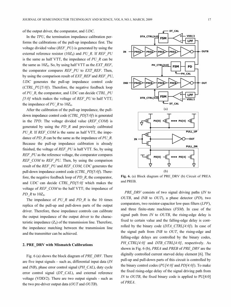
JOURNAL OF SEMICONDUCTOR TECHNOLOGY AND SCIENCE, VOL.9, NO.1, MARCH, 2009 17
of the output driver, the comparator, and UDC. In the TPU, the termination impedance calibration per-
forms the calibrations of the pull-up impedance first. The voltage divided value (REF_PU) is generated by using the external reference resistor (10Z0) and PU_R. If REF_PU is the same as half VTT, the impedance of PU_R can be the same as 10Z0. So, by using half VTT as the EXT_REF, the comparator compares REF_PU to EXT_REF. Then, by using the comparison result of EXT_REF and REF_PU, UDC generates the pull-up impedance control code (CTRL_PU[5:0]). Therefore, the negative feedback loop of PU_R, the comparator, and UDC can decide CTRL_PU [5:0] which makes the voltage of REF_PU to half VTT; the impedance of PU_R to 10Z0.
After the calibration of the pull-up impedance, the pull-down impedance control code (CTRL_PD[5:0]) is generated in the TPD. The voltage divided value (REF_COM) is generated by using the PD_R and previously calibrated PU_R. If REF_COM is the same as half VTT, the impe-dance of PD_R can be the same as the impedance of PU_R. Because the pull-up impedance calibration is already finished, the voltage of REF_PU is half VTT. So, by using REF_PU as the reference voltage, the comparator compares REF_COM to REF_PU. Then, by using the comparison result of the REF_PU and REF_COM, UDC generates the pull-down impedance control code (CTRL_PD[5:0]). There-fore, the negative feedback loop of PD_R, the comparator, and UDC can decide CTRL_PD[5:0] which makes the voltage of REF_COM to the half VTT; the impedance of PD_R to 10Z0.
The impedance of PU_R and PD_R is the 10 times replica of the pull-up and pull-down parts of the output driver. Therefore, these impedance controls can calibrate the output impedance of the output driver to the charac-teristic impedance (Z0) of the transmission line. Therefore, the impedance matching between the transmission line and the transmitter can be achieved.
2. PRE_DRV with Mismatch Calibrations
Fig. 6 (a) shows the block diagram of PRE_DRV. There
are five input signals – such as, differential input data (IN and INB), phase error control signal (PH_CAL), duty cycle error control signal (DT_CAL), and external reference voltage (VDD/2). There are two output signals - such as the two pre-driver output data (OUT and OUTB).
PRE_DRV consists of two signal driving paths (IN to OUTB, and INB to OUT), a phase detector (PD), two comparators, two resistor-capacitor low-pass filters (LPF), and three finite-state machines (FSM). In case of the signal path from IN to OUTB, the rising-edge delay is fixed to certain value and the falling-edge delay is cont-rolled by the binary code (DTA_CTRL[4:0]). In case of the signal path from INB to OUT, the rising-edge and falling-edge delays are controlled by the binary codes, PH_CTRL[4:0] and DTB_CTRL[4:0], respectively. As shown in Fig. 6 (b), PREA and PREB of PRE_DRV are the digitally controlled current starved delay element [6]. The pull-up and pull-down parts of this circuit is controlled by the binary control codes (PU[4:0] and PD[4:0]). To make the fixed rising-edge delay of the signal driving path from IN to OUTB, the fixed binary code is applied to PU[4:0] of PREA.
FSM
PREA OUTB
OUT
IN
INB
FSM+-
PDPH_CTRL[4:0]
PREA PREA PREA
PREB PREB PREB PREB
PH_CAL
DT_CAL
DTA_CTRL[4:0] VDD/2
LPF
FSM+-
DT_CAL
DTB_CTRL[4:0] VDD/2
LPF
(a)
PU[0]
IN OUT
PU[4]
PD[0] PD[4]
PULL_UP
PULL_DN
(b)
Fig. 6. (a) Block diagram of PRE_DRV (b) Circuit of PREA and PREB.

18 JUN-HYUN BAE et al : A LOW-VOLTAGE HIGH-SPEED CMOS INVERTER-BASED DIGITAL DIFFERENTIAL TRANSMITTER WITH…
To calibrate the phase error between two signal driving paths and the duty cycle error of each signal driving path, there are one phase control loop and two duty cycle control loops. The phase control loop consists of one signal driving path (INB to OUT), PD, and FSM which is controlled by PH_CAL. The duty cycle control loop consists of one signal driving path, LPF, the comparator, and FSM which is controlled by DT_CAL. Fig. 7 shows the operation timing diagram of PRE_DRV. During PRE_DRV calibration, by using two MUX (Fig. 2), the input of PRE_DRV is changed from the differential input data to CLK which has the period of T. The PVT variations can cause mismatches in the PRE_DRV. As shown in the first timing diagram, if there is no calibration scheme, two outputs of the PRE_DRV has the phase error (PH. ERR.) between two outputs and duty cycle errors (DT. ERR.) for each output. These errors distort the EYE opening of the transmitter and degrade the transmitter performance.
The phase error between two outputs of the PRE_DRV is caused by the mismatch of the rising-edge delays between two signal driving paths. To correct the phase error, the phase control loop operates as a general digital delay-locked loop. The phase control loop compares the phase difference between OUT and OUTB, and controls the rising-edge delay of OUT to remove the phase error. The rising-edge delay of the signal path from IN to OUTB is fixed. Therefore, as shown in the second timing diagram of Fig. 7, the phase control loop can remove the phase error. This phase control calibrates the rising-edge delay mismatch between two signal driving paths of PRE_DRV.
Although the phase control loop removes the phase
error, the duty cycle errors of each signal driving path are still remained. Therefore, after the calibration of the phase control loop is finished, the duty cycle control loop is activated. The duty cycle errors are caused by the devia-tion of the falling-edge delay. If the time difference bet-ween rising-edge and falling-edge is half period (T/2), the duty cycle of pre-driver output is 50%. However, because of the PVT variations, the falling-edge delay is varied. This variation also distorts the EYE diagram of the pre-driver output and degrades transmitter performance. To correct the duty cycle errors of each signal driving path, two duty cycle control loops are used. If the duty cycle of the pre-driver output is 50%, the averaged value of the pre-driver output will be half VDD. Therefore, by com-paring the averaged value of the pre-driver output to half VDD, each duty cycle control loop controls the falling-edge delay to make the averaged value of the pre-driver output to half VDD. As shown in the third figure of Fig. 7, the duty control loops can correct the duty cycle errors (DT. ERR.) of OUT and OUTB. Because two duty cycle control loops control only the falling-edge delay of two signal paths, the duty cycle control loops do not disturb the calibrated rising-edge delay by the phase control loop. Therefore, these delay controls can calibrate the phase error and the duty cycle errors which are caused by the mismatches of PRE_DRV.
IV. MEASUREMENT RESULTS
The circuit was implemented by using 0.18 μm CMOS process. The chip, shown in Fig. 8, consists of the pro-posed digital differential transmitter and the receiver for
PH. ERR.
OUT
OUTB
OUT
OUTB
DT. ERR.
PHASE CONTROL
OUT
OUTB
DUTY CYCLE CONTROL
DT. ERR.
T/2
T/2
Fig. 7. Operation timing diagram of PRE_DRV calibration.
Digital TX480μm*700μm
RX for testing
Fig. 8. Chip layout.

JOURNAL OF SEMICONDUCTOR TECHNOLOGY AND SCIENCE, VOL.9, NO.1, MARCH, 2009 19
testing. The active chip area of the proposed transmitter is 480 μmⅹ700 μm. The highest data rate of the fabricated chip was 4 Gbps at the supply voltage of 1.2 V. Fig. 9 shows the measured differential output waveforms at the data rate of 2.8 Gbps and the supply voltage of 1 V which is about 2 times the threshold voltage. Fig. 9 (a) shows the measured waveform for the case of turning-off the calib-rations of both the termination impedance and PRE_DRV. In this case, the eye diagram is distorted by the termina-tion impedance mismatch and the phase error between two signal driving paths and the duty cycle errors of each signal driving path of PRE_DRV. Fig. 9 (b) shows the
measured waveform for the case of turning-on only the termination impedance calibration. By calibrating termi-nation impedance, the differential voltage swing is set to VTT/2. Fig. 9 (c) shows the measured result of the calib-rations of both termination impedance and PRE_DRV. Fig. 10 shows the voltage margin and timing margin of the EYE diagram measured at the transmitter output. The termination calibration improved the voltage margin from 80 mV to 210 mV and the timing margin from 230 psec to 250 psec. The mismatch calibration improved the voltage margin from 210 mV to 240 mV and the timing margin from 250 psec to 300 psec. As shown in the figure, the proposed calibration schemes improve the eye opening with the voltage margin by 200% and the timing margin by 30%.
Although the whole calibration sequence is finished, there is some distortion at the eye diagram of Fig. 9 (c). The distortion is caused by the short calibration range of the PRE_DRV calibration. By extending the calibration range, this signal distortion can be perfectly resolved.
The measured performance is summarized in Table 1.
V. CONCLUSIONS
A low-voltage CMOS digital differential transmitter was implemented with PVT mismatch calibration of pre-driver and impedance matching calibration of main driver. To reduce the reflection between the main driver and the
(a)
(b)
(c)
Fig. 9. Measured differential output waveforms @ 2.8Gbps and 1V (a) No calibration (b) DRV(termination) calibration (c)DRV calibration and PRE_DRV(mismatch) calibration.
0.0
50.0p
100.0p
150.0p
200.0p
250.0p
300.0p
No Cal. T_CAL PD_CAL0.0
50.0m
100.0m
150.0m
200.0m
250.0m Voltage Margin
Tim
e [s
ec]
Vol
tage
[V
]
Timing Margin
Fig. 10. Eye opening with the proposed calibrations.
Table 1. Performance summary (measurements). Process 0.18 μm CMOS Circuits Digital TX + RX for test Max. Speed 4Gbps @ 1.2 V Eye Opening No Calibration Term. Calibration PRE_DRV Calibration
@ 2.8 Gbps, 1 V 8 0mV, 230 psec 210 mV, 250 psec 240 mV, 300 psec
Power Consumption (TX) 30 mW @ 2.8 Gbps, 1 V Chip Area (TX) 480 μm 700ⅹ μm

20 JUN-HYUN BAE et al : A LOW-VOLTAGE HIGH-SPEED CMOS INVERTER-BASED DIGITAL DIFFERENTIAL TRANSMITTER WITH…
transmission line, the output impedance of the main driver was calibrated to the characteristic impedance of the transmission line by using external reference resistor. By calibrating the pull-up and pull-down driving strength of the pre-driver, the differential signal distortion of the pre-driver output, which is sensitive to PVT variations, is compensated. The chip was fabricated with 0.18 μm CMOS process which uses the standard supply voltage of 1.8 V. The highest data rate was 4 Gbps at 1.2 V. The calibration schemes improved the output eye opening with the vol-tage margin of 200% and the timing margin of 30%, at 2.8 Gbps and 1 V.
ACKNOWLEDGMENTS
This work was supported by IDEC, and BK21 program, KOREA.
REFERENCES
[1] R. Palmer, et al, “A 14 mW 6.25 Gb/s Transceiver in 90 nm CMOS for Serial Chip-to-Chip Communi-cations,” Solid-State Circuits Conference, 2007. ISSCC 2007. Digest of Technical Papers. IEEE International, 11-15, Feb. 2007, pp. 440-614.
[2] K.-L.J. Wong, et al, “A 27-mW 3.6-gb/s I/O tran-sceiver,” Solid-State Circuits, IEEE Journal of, vol. 39, Issue 4, April 2004, pp.602-612.
[3] Y. C. Jang, J. H. Bae, and H. J. Park, “A Digital CMOS PWCL With Fixed-Delay Rising Edge and Digital Stability Control,” Circuits and Systems II, IEEE Transactions on, vol. 53, Issue 10, Oct. 2006, pp.1063-1067.
[4] Peng Xu and P. Abshire, “Stochastic Behavior of a CMOS Inverter,” Electronics, Circuits and Systems, 2007, ICECS 2007, 14th IEEE International Con-ference on, 11-14 Dec. 2007, pp.94-97.
[5] L. Bisdounis, S. Nikolaidis, and O. Loufopavlou, “Propagation delay and short-circuit power dissi-pation modeling of the CMOS inverter,” Circuits and Systems I: Fundamental Theory and Applica-tions, IEEE Transactions on, vol. 45, Issue 3, March 1998, pp.259-270.
[6] M. Maymandi-Nejad and M. Sachdev, “A monotonic digitally controlled delay element,” Solid-State Cir-cuits, IEEE Journal of, vol. 40, Issue 11, Nov. 2005, pp.2212-2219.
Jun Hyun Bae was born in Ui-Seong, Korea, on 1981. He received the B.S. degree in the Department of Electronic and Electrical Engineering from Kyung-Pook National University, Korea, in 2004 and M.S. degree in Electronic Engineering from Pohang
University of Science and Technology (POSTECH), Korea, in 2007, respectively. He is currently pursuing the Ph.D. degree in the Department of Electronic and Electrical Engineering from Pohang University of Science and Technology (POSTECH), Korea. His interests include data converters, high-speed interface circuits and ultra-low-voltage analog circuits.
Sang-Hune Park received the B.S., M.S., Ph.D. degrees in the Department of Electrical Engineering from Pohang University of Science and Technology, Pohang, Korea, in 2000, 2002, and 2008, respectively. In 2008, he joined at Samsung Electronics, where he has
been working in the area of high-speed interface circuit design. His interests include high speed CMOS circuit design and digital mixed-signal ICs.
Jae-Yoon Sim received the B.S., M.S., and Ph.D. degrees in Electronic and Electrical Engineering from Pohang University of Science and Technology, Korea, in 1993, 1995, and 1999, res-pectively. From 1999 to 2005, he was a Senior Engineer at Samsung Elec-
tronics, Korea. From 2003, to 2005, he was a post-doctoral student with the University of Southern California, Los Angeles. In 2005, he joined the Faculty of Electronic and Electrical Engineering, Pohang University of Science and Technology, Korea, where he is currently an Assistant Professor. His research interests include PLL/DLL, high-speed links, memory circuits, and ultra low-power analog.

JOURNAL OF SEMICONDUCTOR TECHNOLOGY AND SCIENCE, VOL.9, NO.1, MARCH, 2009 21
Hong June Park received the B.S. degree from the Department of Elec-tronic Engineering, Seoul National University, Seoul, Korea, in 1979, the M.S. degree from the Korea Advanced Institute of Science and Technology, Taejon, in 1981, and the Ph.D. degree
from the Department of Electrical Engineering and Com-puter Sciences, University of California, Berkeley, in 1989. He was a CAD engineer with ETRI, Korea, from 1981 to 1984 and a Senior Engineer in the TCAD Department of Intel from 1989 to 1991. In 1991, he joined the Faculty of Electronic and Electrical Engineering, Pohang University of Science and Technology (POSTECH), Kyungbuk, Korea, where he is currently Professor. His research interests include high-speed CMOS interface circuit design, signal integrity, device and interconnect modeling. Prof. Park is a member of IEEK, IEEE and IEICE.