A hybrid optical packet and wavelength selective switching...
10
A hybrid optical packet and wavelength selective switching platform for high-performance data center networks Lin Xu, 1,* Wenjia Zhang, 1,3 Hugo L. R. Lira, 2 Michal Lipson, 2 and Keren Bergman 1 1 Department of Electrical Engineering, Columbia University, New York, New York 10027, USA 2 School of Electrical and Computer Engineering, Cornell University, Ithaca, New York 14853, USA 3 Institution of Information Photonics and Optical Communications, Beijing University of Posts and Telecommunications, Beijing, 100876, China *[email protected] Abstract: We propose and experimentally demonstrate for the first time a hybrid optical packet and wavelength selective switching platform for high- performance data center networks. This architecture based on cascaded silicon microrings and semiconductor optical amplifiers (SOAs) supports wavelength reconfigurable packet and circuit switching, and is highly scalable, energy efficient and potentially integratable. By combining the wavelength-selective behavior of the microring and the broadband behavior of the SOA switch, we are able to achieve fast switching transitions, high extinction ratios, and low driving voltages, which are all requirements for future optical high-performance data center networks. Routing correctness and error-free operation (<10 −12 ) are verified for both 10-Gb/s and 40-Gb/s packets and streaming data with format transparency. ©2011 Optical Society of America OCIS codes: (060.4253) Networks, circuit-switched; (060.4259) Networks, packet-switched; (250.3140) Integrated optoelectronic circuits; (230.3120) Integrated optics devices; (200.4650) Optical interconnects. References 1. J. Hamilton, “Cooperative expendable micro-slice servers (CEMS): low cost, low power servers for internet- scale services,” presented at 4th Biennial Conference on Innovative Data Systems Research (CIDR) Asilomar, California, USA, Jan. 4–7, 2009. 2. A. Greenberg, J. R. Hamilton, N. Jain, S. Kandula, C. Kim, P. Lahiri, D. A. Maltz, P. Patel, and S. Sengupta, “VL2: a scalable and flexible data center network,” in Proceedings of the ACM SIGCOMM 2009 Conference on Data Communication (ACM, 2009), pp. 63–74. 3. T. Benson, A. Anand, A. Akella, and M. Zhang, “Understanding data center traffic characteristics,” in WREN '09 Proceedings of the 1st ACM Workshop on Research on Enterprise Networking (ACM, 2009), pp. 65–72. 4. C. Lam, H. Liu, B. Koley, X. Zhao, V. Kamalov, and V. Gill, “Fiber optic communication technologies: what’s needed for datacenter network operations,” IEEE Commun. Mag. 48(7), 32–39 (2010). 5. M. Al-Fares, A. Loukissas, and A. Vahdat, “A scalable, commodity data center network architecture,” in SIGCOMM '08 Proceedings of the ACM SIGCOMM 2008 Conference on Data Communication (ACM, 2008), pp. 63–74. 6. G. Astfalk, “Why optical data communications and why now,” Appl. Phys. A Mater. Sci. Process. 95(4), 933– 940 (2009). 7. O. Liboiron-Ladouceur, A. Shacham, B. A. Small, B. G. Lee, H. Wang, C. P. Lai, A. Biberman, and K. Bergman, “The data vortex optical packet switched interconnection network,” J. Lightwave Technol. 26(13), 1777–1789 (2008). 8. R. P. Luijten and R. Grzybowski, “The Osmosis optical packet switch for supercomputers,” in Optical Fiber Communication Conference, OSA Technical Digest (CD) (Optical Society of America, 2009), paper OTuF3. 9. X. Ye, P. Mejia, Y. Yin, R. Proietti, S. J. B. Yoo, and V. Akella, “DOS—a scalable optical switch for datacenters,” in ANCS '10 Proceedings of the 6th ACM/IEEE Symposium on Architectures for Networking and Communications Systems (ACS, 2010), article 24. 10. N. Farrington, G. Porter, S. Radhakrishnan, H. H. Bazzaz, V. Subramanya, Y. Fainman, G. Papen, and A. Vahdat, “Helios: a hybrid electrical/optical switch architecture for modular data centers,” in SIGCOMM '10 Proceedings of the ACM SIGCOMM 2010 Conference on SIGCOMM (ACM, 2010), pp. 339–350. #153448 - $15.00 USD Received 26 Aug 2011; revised 22 Oct 2011; accepted 25 Oct 2011; published 14 Nov 2011 (C) 2011 OSA 21 November 2011 / Vol. 19, No. 24 / OPTICS EXPRESS 24258
Transcript of A hybrid optical packet and wavelength selective switching...

A hybrid optical packet and wavelength selective switching platform for
high-performance data center networks Lin Xu,1,* Wenjia Zhang,1,3 Hugo L. R. Lira,2 Michal Lipson,2 and Keren Bergman1
1Department of Electrical Engineering, Columbia University, New York, New York 10027, USA 2School of Electrical and Computer Engineering, Cornell University, Ithaca, New York 14853, USA
3Institution of Information Photonics and Optical Communications, Beijing University of Posts and Telecommunications, Beijing, 100876, China
Abstract: We propose and experimentally demonstrate for the first time a hybrid optical packet and wavelength selective switching platform for high-performance data center networks. This architecture based on cascaded silicon microrings and semiconductor optical amplifiers (SOAs) supports wavelength reconfigurable packet and circuit switching, and is highly scalable, energy efficient and potentially integratable. By combining the wavelength-selective behavior of the microring and the broadband behavior of the SOA switch, we are able to achieve fast switching transitions, high extinction ratios, and low driving voltages, which are all requirements for future optical high-performance data center networks. Routing correctness and error-free operation (<10−12) are verified for both 10-Gb/s and 40-Gb/s packets and streaming data with format transparency. ©2011 Optical Society of America OCIS codes: (060.4253) Networks, circuit-switched; (060.4259) Networks, packet-switched; (250.3140) Integrated optoelectronic circuits; (230.3120) Integrated optics devices; (200.4650) Optical interconnects.
References 1. J. Hamilton, “Cooperative expendable micro-slice servers (CEMS): low cost, low power servers for internet-
scale services,” presented at 4th Biennial Conference on Innovative Data Systems Research (CIDR) Asilomar, California, USA, Jan. 4–7, 2009.
2. A. Greenberg, J. R. Hamilton, N. Jain, S. Kandula, C. Kim, P. Lahiri, D. A. Maltz, P. Patel, and S. Sengupta, “VL2: a scalable and flexible data center network,” in Proceedings of the ACM SIGCOMM 2009 Conference on Data Communication (ACM, 2009), pp. 63–74.
3. T. Benson, A. Anand, A. Akella, and M. Zhang, “Understanding data center traffic characteristics,” in WREN '09 Proceedings of the 1st ACM Workshop on Research on Enterprise Networking (ACM, 2009), pp. 65–72.
4. C. Lam, H. Liu, B. Koley, X. Zhao, V. Kamalov, and V. Gill, “Fiber optic communication technologies: what’s needed for datacenter network operations,” IEEE Commun. Mag. 48(7), 32–39 (2010).
5. M. Al-Fares, A. Loukissas, and A. Vahdat, “A scalable, commodity data center network architecture,” in SIGCOMM '08 Proceedings of the ACM SIGCOMM 2008 Conference on Data Communication (ACM, 2008), pp. 63–74.
6. G. Astfalk, “Why optical data communications and why now,” Appl. Phys. A Mater. Sci. Process. 95(4), 933–940 (2009).
7. O. Liboiron-Ladouceur, A. Shacham, B. A. Small, B. G. Lee, H. Wang, C. P. Lai, A. Biberman, and K. Bergman, “The data vortex optical packet switched interconnection network,” J. Lightwave Technol. 26(13), 1777–1789 (2008).
8. R. P. Luijten and R. Grzybowski, “The Osmosis optical packet switch for supercomputers,” in Optical Fiber Communication Conference, OSA Technical Digest (CD) (Optical Society of America, 2009), paper OTuF3.
9. X. Ye, P. Mejia, Y. Yin, R. Proietti, S. J. B. Yoo, and V. Akella, “DOS—a scalable optical switch for datacenters,” in ANCS '10 Proceedings of the 6th ACM/IEEE Symposium on Architectures for Networking and Communications Systems (ACS, 2010), article 24.
10. N. Farrington, G. Porter, S. Radhakrishnan, H. H. Bazzaz, V. Subramanya, Y. Fainman, G. Papen, and A. Vahdat, “Helios: a hybrid electrical/optical switch architecture for modular data centers,” in SIGCOMM '10 Proceedings of the ACM SIGCOMM 2010 Conference on SIGCOMM (ACM, 2010), pp. 339–350.
#153448 - $15.00 USD Received 26 Aug 2011; revised 22 Oct 2011; accepted 25 Oct 2011; published 14 Nov 2011(C) 2011 OSA 21 November 2011 / Vol. 19, No. 24 / OPTICS EXPRESS 24258

11. G. Wang, D. G. Andersen, M. Kaminsky, K. Papagiannaki, T. E. Ng, M. Kozuch, and M. Ryan, “c-Through: part-time optics in data centers,” in SIGCOMM '10 Proceedings of the ACM SIGCOMM 2010 conference on SIGCOMM (ACM, 2010), pp. 327-338.
12. A. Singla, A. Singh, K. Ramachandran, L. Xu, and Y. Zhang, “Proteus: a topology malleable data center networks,” in Hotnets '10 Proceedings of the Ninth ACM SIGCOMM Workshop on Hot Topics in Networks (ACM, 2010), article 8.
13. A. Shacham and K. Bergman, “An experimental validation of a wavelength-striped, packet switched, optical interconnection network,” J. Lightwave Technol. 27(7), 841–850 (2009).
14. H. Wang, A. S. Garg, and K. Bergman, “Design and demonstration of all-optical hybrid packet and circuit switched network platform for next generation data center,” in Optical Fiber Communication Conference, OSA Technical Digest (CD) (Optical Society of America, 2010), paper OTuP3.
15. M. Glick, “Optical interconnects in next generation data centers: an end to end view,” in 2008 16th IEEE Symposium on High Performance Interconnects (IEEE, 2008), pp. 178–181.
16. H. Wang and K. Bergman, “A bidirectional 2×2 photonic network building-block for high-performance data centers,” in Optical Fiber Communication Conference, OSA Technical Digest (CD) (Optical Society of America, 2011), paper OTuH4.
17. A. Biberman, H. L. R. Lira, K. Padmaraju, N. Ophir, J. Chan, M. Lipson, and K. Bergman, “Broadband silicon photonic electrooptic switch for photonic interconnection networks,” IEEE Photon. Technol. Lett. 23(8), 504–506 (2011).
18. L. Xu, J. Chan, A. Biberman, H. L. R. Lira, M. Lipson, and K. Bergman, “DPSK transmission through silicon microring switch for photonic interconnection networks,” IEEE Photon. Technol. Lett. 23(16), 1103–1105 (2011).
19. C. P. Lai, D. Brunina, and K. Bergman, “Demonstration of 8×40 Gb/s wavelength striped packet switching in a multi-terabit capacity optical network testbed,” in Proceedings of 23rd Annual Meeting of the IEEE Photonics Society (IEEE, 2010), paper ThQ2
20. H. L. R. Lira, S. Manipatruni, and M. Lipson, “Broadband hitless silicon electro-optic switch for on-chip optical networks,” Opt. Express 17(25), 22271–22280 (2009).
21. C. P. Lai, A. Shacham, and K. Bergman, “Demonstration of asynchronous operation of a multiwavelength optical packet-switched fabric,” IEEE Photon. Technol. Lett. 22(16), 1223–1225 (2010).
22. Q. Xu, D. Fattal, and R. G. Beausoleil, “Silicon microring resonators with 1.5-microm radius,” Opt. Express 16(6), 4309–4315 (2008).
1. Introduction
The tremendous growth in cloud computing applications is driving the creation of numerous data centers including mega-data centers (DCs) which can consist of over 100,000 servers [1]. As these DCs continue to grow in support of the bandwidth hungry applications, demand for increased communications bandwidths is straining the server interconnection networks. Beyond the sheer growth in traffic volume, network monitoring in DCs shows that traffic patterns, consisting of both small (a few KB) and long-lived (100-1000 MB) messages, are highly divergent and unpredictable [2,3]. Existing electrically switched DC networks, created by commodity Ethernet switches and routers, have not been able to meet these massively increasing and heterogeneous bandwidth demands without exorbitant increases in cost and power [4]. Even though there have been considerable efforts in designing innovative architectures [2,5], these proposals are ultimately constrained by fundamental electronics properties and will not be able to scale to meet the relentless demands for increased connectivity and bandwidth in an energy efficient manner [6]. Optical interconnects are characterized by a high bandwidth-distance product, bit-rate transparency, and low power consumption, and is an attractive solution for addressing the emerging DC interconnect bottleneck. Wavelength-division-multiplexing (WDM) and high-radix switching can scale to provide ~Tb/s/link transmission capacity with potential interconnectivity for tens of thousands of nodes [7–9]. However, key challenges remain on how to deploy optical telecom technologies within the DC environment.
Optical switching technologies developed primarily for telecom applications are challenged in addressing both the traffic diversity and scalability requirements of the DC environment. Current efforts on inserting optical interconnect platforms within the DC environment such as Helios and c-through [10,11] present micro-electro-mechanical switch (MEMS) based hybrid electrical/optical switch architectures that cleverly augment existing electronic packet switching (EPS) hierarchy. The rack-to-rack interconnects developed under
#153448 - $15.00 USD Received 26 Aug 2011; revised 22 Oct 2011; accepted 25 Oct 2011; published 14 Nov 2011(C) 2011 OSA 21 November 2011 / Vol. 19, No. 24 / OPTICS EXPRESS 24259
these efforts successfully achieve reduced complexity high bandwidth communications at significant reductions in cost and power. Furthermore, Proteus [12], a recently proposed a DC network architecture based on optical wavelength/space switches, realized topology malleability according to traffic demand by leveraging optical WDM parallelism and wavelength routing flexibility. The drawback of MEMS based switching however is their relatively slow (10s of ms) reconfiguration time, which cannot accommodate the unpredictable burst traffic behavior of heterogeneous DC applications. Optical packet switching (OPS) networks [13] on the other hand can enable ultra-high bandwidth at nanosecond-scale switching time but suffer from fundamental scalability challenges due to the lack of viable optical buffering technology. To meet the growing demands of DCs, future optical interconnection networks will need to route both packet and circuit traffic in an agile and highly scalable platform [14–16].
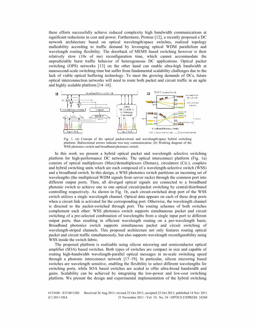
Fig. 1. (a) Concept of the optical packet/circuit and wavelength/space hybrid switching platform. Bidirectional arrows indicate two-way communication. (b) Working diagram of the WSS photonics switch and broadband photonics switch.
In this work we present a hybrid optical packet and wavelength selective switching platform for high-performance DC networks. The optical interconnect platform (Fig. 1a) consists of optical multiplexers (Mux)/demultiplexers (Demux), circulators (Cir.), couplers and hybrid switching units which are each composed of a wavelength-selective switch (WSS) and a broadband switch. In this design, a WSS photonics switch partitions an incoming set of wavelengths (the multiplexed WDM signals from server racks) through the common port into different output ports. Then, all diverged optical signals are connected to a broadband photonic switch to achieve one to one optical circuit/packet switching by central/distributed controlling respectively. As shown in Fig. 1b, each circuit-switched drop port of the WSS switch utilizes a single wavelength channel. Optical data appears on each of these drop ports when a circuit link is activated for the corresponding port. Otherwise, the wavelength channel is directed to the packet-switched through port. The routing schemes of both switches complement each other: WSS photonics switch supports simultaneous packet and circuit switching of a pre-selected combination of wavelengths from a single input port to different output ports, thus resulting in efficient wavelength routing on a per-wavelength basis; Broadband photonics switch supports simultaneous packet and circuit switching of wavelength-striped channels. This proposed architecture not only features routing optical packet and circuit traffic simultaneously, but also supports wavelength reconfigurability using WSS inside the switch fabric.
The proposed platform is realizable using silicon microring and semiconductor optical amplifier (SOA) based switches. Both types of switches are compact in size and capable of routing high-bandwidth wavelength-parallel optical messages in ns-scale switching speed through a photonic interconnect network [17–19]. In particular, silicon microring based switches are wavelength sensitive, enabling the flexibility to select different wavelengths for switching ports, while SOA based switches are scaled to offer ultra-broad bandwidth and gains. Scalability can be achieved by integrating the low-power and low-cost switching platform. We present the design and experimental implementation of the hybrid switching
#153448 - $15.00 USD Received 26 Aug 2011; revised 22 Oct 2011; accepted 25 Oct 2011; published 14 Nov 2011(C) 2011 OSA 21 November 2011 / Vol. 19, No. 24 / OPTICS EXPRESS 24260

platform where aggregated wavelength-striped packets and circuit streams can be routed simultaneously. Section 2 introduces the switch architecture and devices we used to develop the testbed, followed by experiment setup for switching both 10-Gb/s and 40-Gb/s data in section 3. The experiment results are shown in Section 4 verifying the feasibility of the proposed hybrid switch for future high-performance DC networks. The conclusion is performed in Section 5.
2. Architecture and devices
Fig. 2. A schematic hybrid switching architecture consisting of microring resonators, SOAs, PIN photodetectors, electronic control logic circuits as well as passive optical elements (i.e. couplers and wavelength filters).
Figure 2 depicts a schematic diagram of the reconfigurable optical packet and circuit hybrid switch for DC networks. The switch fabric consists of microring resonators, SOAs, PIN photodetectors, electronic control logic circuits as well as passive optical elements (i.e. couplers and wavelength filters). The number of wavelength channels used for packet switching can be dynamically adjusted. Compared to sending the laser outputs directly into broadband photonics switch, having the WSS photonics switch may reduce the number of ports on the broadband switch. However, more importantly, the WSS enables a dynamic allocation of wavelength channels which can be adjusted based on the needs of the data-center server. The system can utilize the high-bandwidth links of circuit switching for applications with long-lived data streams, or can leverage the flexibility of packet switching for applications with small bursty random data packets. Moreover, wavelength channels can be dynamically added to the wavelength-striped packet switched port if additional throughput is required. This functionality of wavelength channel allocation would not be possible in the broadband switch alone. The cascaded microrings switch first selects different data wavelengths onto the corresponding outputs in the manner of WSS before entering the broadband SOA switch which further direct incoming data to the destination outputs in the manner of broadband switch. Within this design, each wavelength channel of input port of the hybrid switch fabric can be switched to any output port of the hybrid switch fabric independently either in packets or streams depending on the traffic demands. The number of wavelength channels used for packet switching can be dynamically adjusted. Compared to sending the laser outputs directly into broadband photonics switch, having WSS photonics switch brings the advantage that the number of ports on the broadband photonics switch will be significantly reduced, which will minimize the SOA power consumption as well as header and frame wavelengths used. Both the switches are controlled by electronic control logic circuit generated from programmable logic elements while the control signal can be extract from a subset of dedicated wavelengths in the manner of distribution control.
Figure 3a illustrates how incoming wavelength channels can be spectrally positioned with respect to the resonances of cascaded microrings. In the passive state (without RF voltage applied to microrings), the wavelength channels on-resonance are routed to the corresponding drop port while the wavelength channels off-resonance are routed to the common through
#153448 - $15.00 USD Received 26 Aug 2011; revised 22 Oct 2011; accepted 25 Oct 2011; published 14 Nov 2011(C) 2011 OSA 21 November 2011 / Vol. 19, No. 24 / OPTICS EXPRESS 24261

Fig. 3. (a) WDM channels positioning (arrows) respective to the optical spectrum of two cascaded microring switch in passive and active states. (b-e) Four possible configurations of the wavelength-selective spatially routed switch. (f) Schematic diagrams of the wavelength-striped packet switching and circuit switching, depicting the optical frame, address and data.
port. In the active state (with RF voltage applied to microrings), the wavelength channels which were previously on-resonance together with those off-resonance are routed to the common through port. Figures 3b–e illustrate the four possible routing configurations of using two cascaded microring switches, showcasing the independent routing of each WDM partition. Figure 3f shows schematic diagrams of the wavelength-striped packet switching and WDM circuit switching [13]. The frame bit denotes the message existence, while address bit indicates the requested output port. Initially, all the data wavelength channels are positioned on-resonance respectively while the entire frame and address wavelength channels are positioned off-resonance. For those wavelength channels in circuit switching mode (Fig. 3f right), the corresponding microrings retain in the passive state thus the required long lived data channels initially positioned on resonances are routed to the corresponding drop port. In parallel, for those wavelength channels in packet switching mode (Fig. 3f left), the corresponding microrings are actively switched thus the wavelength-striped packet channels initially on-resonance are now routed to the common through port. As a result, the formation of wavelength-striped packets can be flexible according to the system requirement. Header information for wavelength-striped optical packets are extracted and analyzed in the switching node, where address information indicates packets are routed to the common through port by actively switching the microrings and subsequently to destination ports by distributed control of SOA switches. There is no header information for circuit switching as the streams are routed by established optical circuits.
Fig. 4. (a) Top-view scanning-electron-microscope (SEM) image of the silicon microring device. (b) Experimental 2x2 switch is comprised of SOAs, optical couplers (ellipses, with coupling ratios), wavelength filters (λ), PIN receivers (O/E), optical fibers, and an electronic control circuit implemented by a complex programmable logic device (CPLD).
The silicon microring device used here (Fig. 4a) is a second-order 1 × 2 switch consisting of two microring resonators, coupled together and to two adjacent waveguides, further details can be found in ref [20]. The resonance wavelength can be shifted by injecting electrical carriers into the corresponding microring cavity through a PIN diode, thus allowing an optical signal to be switched between the through port (off resonance) and drop port (on resonance). The SOA switch used here (Fig. 4b) is built with 2 × 2 photonic switching node, consisting of four SOAs that provide a broadband gain spectrum (C & L bands), fast switching times (< ns) and data-rate transparency . The prototype switching nodes have been demonstrated by using
#153448 - $15.00 USD Received 26 Aug 2011; revised 22 Oct 2011; accepted 25 Oct 2011; published 14 Nov 2011(C) 2011 OSA 21 November 2011 / Vol. 19, No. 24 / OPTICS EXPRESS 24262

commercially-available, discrete-packaged components such as passive optical devices, high speed electronic circuitry and SOAs [13] and have potentials to be integrated. The same switching node has been demonstrated to perform functionalities, such as address encoding/decoding, correct routing, error-free transmission of wavelength-striped optical messages as well as asynchronously routing variable-length messages [13,19,21].
This proposed switching architecture features the flexibility to support both optical circuit switching and packet switching. Photonic integrated circuit (PIC) technology can simplify the encoding and decoding of the multiple-wavelength messages. The frame, address and payload wavelengths propagate together as a wavelength strip in the network. Group velocity dispersion caused wavelength walk-off is negligible since the propagation distances associated with the networks considered here are less than hundreds of meters for the largest scale systems.
3. Experiment setup
Fig. 5. Experimental setup using the silicon electro-optic microring WSS switch and SOA
based broadband switch.
The experimental setup (Fig. 5) is comprised of three continuous wave (CW) light sources from tunable lasers (TL1, TL2, TL3), centered at 1541.7 nm, 1535.05 nm and 1555.75 nm respectively. The CW light from TL1 is first modulated by an external 10-Gb/s modulator (phase modulator or amplitude modulator) driven with a 10-Gb/s, non-return-to-zero (NRZ), 231–1 pseudo-random bit sequence (PRBS) pattern from a pulse pattern generator (PPG), then transmitted through 1-km single mode fiber (SMF) and gated by a SOA to create packetized data. The other two CW light from TL2 and TL3 are gated by separated SOAs to create frame and address signals. They are then combined with the packetized data using fiber couplers, and are synchronized in time to ensure the frame, address and data packets perfectly overlap. All the signals are aligned to quasi-TM polarization before being coupled into the on-chip nano-tapered silicon waveguide using a tapered fiber. For experimental simplicity, the microring device is switched by a data timing generator (DTG) through chip contracts with high-speed RF probes with a 0.9-VPP square wave and a 1.0-V voltage bias. The fiber-to-fiber insertion loss is 16 dB for the through port and 18 dB for the drop port.
Figure 6a shows the through port and drop port spectra of the microring device in the passive state (without RF driving signal) scanned with 0.003-nm step, showing a 9-nm free spectral range (FSR), through-port extinction ratio of 15 dB, and passband with 3-dB bandwidths of 20 GHz. The microring used in the experiment has a radius of 10 μm. A WSS consisted of cascaded microrings can support about 4 wavelength channels with each working at 40 Gb/s maximum. Microrings with radius as small as 1.5 μm have been demonstrated elsewhere [22]. Since the FSR of a single-ring device is inversely proportional to the ring radius, the smaller microring can be used to enlarge the FSR. In addition, higher-order
#153448 - $15.00 USD Received 26 Aug 2011; revised 22 Oct 2011; accepted 25 Oct 2011; published 14 Nov 2011(C) 2011 OSA 21 November 2011 / Vol. 19, No. 24 / OPTICS EXPRESS 24263

Fig. 6. (a) The through port and drop port spectra of the microring device in the passive state. (b) Spectrum of the input WDM channels for address, frame and signal.
coupled microrings can offer a box-like passband with sharper roll-off. Meanwhile, a smaller number of ports compared to electronics are needed to connect several racks since optical switching would initially only be used in the core or aggregation node of the datacenter interconnection network [5]. With these considerations, sufficiently large FSR and extinction ratio can be engineered. The passbands of the two microring cavities are not perfectly overlapping in the passive state for this particular device; however, these passbands are aligned with the applied voltage bias during active switching, and has been shown to achieve extinction ratios greater than 20 dB [20]. As shown in Fig. 6b, the signal wavelength (1541.7 nm) is on resonance while the frame and address wavelengths (1535.05 nm and 1555.75 nm) are off-resonance. Thus the switching of the microring affects the signal channel only.
The optical signals egressing from the chip are amplified by an erbium-doped fiber amplifier (EDFA) and sent to the input port (in0) of the 2x2 SOA switch. After the switch, the output signals are filtered (λ) to suppress the power of frame and address signals. DPSK signal is additionally demodulated by a delay interferometer (DI). Finally, the filtered signal passes through a variable optical attenuator (VOA) and is detected using a photodetector (PIN-TIA) followed by a limiting amplifier (LA), and examined on a 10-Gb/s bit-error rate tester (BERT). The DTG gates the BERT over the duration of each optical packet. All the clock sources are synchronized. A DCA is used to evaluate the temporal performance.
For 40-Gb/s experiment, we use the same setup except that: the signal is generated by passing the CW lightwave through a 40-Gb/s amplitude modulator which is driven with 40-Gb/s, NRZ, 215–1 PRBS pattern from a PPG. No 1-km SMF is used in this case. At the receiver side, the signal is received by a high-speed PIN photodiode and trans-impedance amplifier (PIN-TIA) followed by a limiting amplifier (LA). The received 40-Gb/s data is spatially demultiplexed into four 10-Gb/s electrical data streams using an electrical demultiplexer (DEMUX), and one of which is evaluated using a 10-Gb/s BERT.
4. Results
To demonstrate the correct routing functionality for the switch fabric test-bed, we first switch 10-Gb/s amplitude-shift-keyed (ASK) signal in both packet switching mode and circuit switching mode. For packet switching, we produce 59-ns optical data packets with 128-ns period using a gating signal of 46% duty cycle. The frame and address are created to have the same packet length. The total average optical power injected into the silicon chip is 1 dBm. Since the data wavelength is initially set on-resonance, data stream is routed to the drop port
#153448 - $15.00 USD Received 26 Aug 2011; revised 22 Oct 2011; accepted 25 Oct 2011; published 14 Nov 2011(C) 2011 OSA 21 November 2011 / Vol. 19, No. 24 / OPTICS EXPRESS 24264

Fig. 7. Experimental waveforms showing the correct routing functionality of the optical packets. In: the input port of the microring switch; Out0 and Out1: the output ports of 2x2 SOA switch.
in the passive state for circuit switching while packetized data is routed to the through port in the active state for packet switching. We actively switch the microring device with the same period but slightly larger duty cycle to fully cover the data packets. Within the microring’s switching window, all the packets coming into the input port of the microring are routed to the through port where they are launched into the input port (In0) of the 2x2 SOA switch. For logic 1 (Fig. 7a), all the packets are routed to the output port (Out0). For logic 2 (Fig. 7b), one packet is routed to the output port (Out1) while the others are routed to the output port (Out0). After demonstrating correct routing of the packets, we show circuit switching logic (Fig. 7c) by passing a continuous data through the microring passively. The data egressing from the drop port of the microring is launched into the input port (In0) of the 2x2 SOA switch and then routed to the output port (Out1) by established circuit.
Fig. 8. BER curves for the input and output 10-Gb/s signals and respective eye-diagrams in (a) ASK format, circuit switching (b) ASK format, packet switching (c) DPSK format, circuit switching and (d) DPSK format, packet switching. Input and output refer to the input port and output port of the switch fabric test-bed shown in Fig. 5.
#153448 - $15.00 USD Received 26 Aug 2011; revised 22 Oct 2011; accepted 25 Oct 2011; published 14 Nov 2011(C) 2011 OSA 21 November 2011 / Vol. 19, No. 24 / OPTICS EXPRESS 24265

We further evaluate the test-bed performance by measuring the power penalty between the data before and after the switch fabric test-bed for both circuit switching and packet switching, working at different modulation formats. 10-Gb/s BER curves and the corresponding input and output eye diagrams for ASK (Figs. 8a–b) and DPSK (Figs. 8c–d) signals are recorded. The back-to-back for each case is measured individually at the input of the switch fabric test-bed. In order to account for differences in average measured power at the receiver, the duty cycle correction is performed by shifting 3.1 dB for the packetized signal based on 46% duty cycle and 13-dB extinction ratio of the gating signal. There is 0.2-dB power penalty observed for both circuit and packet switching for ASK signal; 0.4-dB and 0.2-dB power penalties for circuit switching and packet switching respectively for DPSK signal. Error-free operation (defined as having BERs less than 10−12) is achieved for all the above cases, validating the network’s error-free performance and format transparency.
We then switch 40-Gb/s ASK signal through the switch fabric test-bed, and record the BER curves as well as the corresponding eye diagrams for both circuit switching (Fig. 9a) and packet switching (Fig. 9b). For packet switching, we produce 48-ns optical data packets using 64-ns period with a 75% duty cycle gating signal. The total average optical power injected into the silicon chip is −4 dBm. We actively switch the microring device and route the packets to the through port. The packets egressing the chip are further switched by the 2x2 SOA switch and routed to the output port (Out0). For circuit switching, 40-Gb/s continuous data at on-resonance wavelength passes through the microring without applying driving voltage therefore being routed to the drop port of the microring. The data egressing from the drop port is launched into the input port (In0) of the 2x2 SOA switch and then routed to the output port (Out1). In order to account for differences in average measured power at the receiver, the duty cycle correction is performed by shifting 1.17 dB for the packetized signal based on 75% duty
Fig. 9. BER curves for the input and output 40-Gb/s ASK signals and respective eye-diagrams in (a) circuit switching (b) packet switching. Input and output refer to the input port and output port of the switch fabric test-bed shown in Fig. 5.
#153448 - $15.00 USD Received 26 Aug 2011; revised 22 Oct 2011; accepted 25 Oct 2011; published 14 Nov 2011(C) 2011 OSA 21 November 2011 / Vol. 19, No. 24 / OPTICS EXPRESS 24266

cycle and 13-dB extinction ratio of the gating signal. The different back-to-back sensitivity between the 40-Gb/s signal in circuit switching and that in packet switching is due to the performance variation of the 40-Gb/s receiver components between the packetized data and stream data. We observe 1.2-dB and 0.6-dB power penalties for circuit switching and packet switching respectively. The additional power penalty for the circuit switching compared to the packet switching is attributed to spectral altering of the 40-Gb/s signal sidebands through the microring as well as non-linear phase response within the resonance of the coupled microrings. Data signals that are routed to the drop port during circuit-switching operation experience an induced phase shift (leading to chromatic dispersion) and spectrum filtering (leading to unbalanced spectrum) from entering the microring. However, the signals that are routed to the through port during packet-switched operation do not enter the microring cavity and therefore do not experience the aforementioned effects.
5. Conclusion
We have demonstrated routing through the hybrid switch fabric test-bed for both packets and data stream with correct logics, and further characterized 10-Gb/s signals in both ASK and DPSK formats as well as 40-Gb/s ASK signal. Error-free operations (BER<10−12) are achieved for all the configurations with negligible power penalties at 10 Gb/s. By combining the wavelength-selective behavior of the microring and the broadband behavior of the SOA switch, the proposed hybrid switching platform provide a real prototype of reconfigurable photonic networking testbed for verifying the feasibility of routing ultrahigh bandwidth long-lived streams in circuit switching mode; and ultrahigh bandwidth wavelength-striped packets in packet switching mode with short switching transitions, high extinction ratios, low driving voltage. The potential of integrated hybrid switching module will lead to significant cost and power savings over conventional discrete optical components designs, scalable for future optical high-performance DC networks.
Acknowledgments
This work was supported in part by the National Science Foundation and Semiconductor Research Corporation under Grant ECCS-0903406 SRC Task 2001. The authors would like to thank Johnnie Chan and Lee Zhu for technical suggestions. Hugo Lira thanks his sponsorship support provided by the Brazilian Defense Ministry.
#153448 - $15.00 USD Received 26 Aug 2011; revised 22 Oct 2011; accepted 25 Oct 2011; published 14 Nov 2011(C) 2011 OSA 21 November 2011 / Vol. 19, No. 24 / OPTICS EXPRESS 24267