A General Approach to MEMS Reliability Assurance - NASA · PDF fileA General Approach to MEMS...
20
NEPP-1, 5/16/01 NEPP/EPAR A General Approach to MEMS Reliability Assurance Joanne Wellman--JPL This work was carried out at the Jet Propulsion Laboratory, California Institute of Technology, under contract with the National Aeronautics and Space Administration, Code AE, under the NASA Electronics Parts and Packaging Program (NEPP)
Transcript of A General Approach to MEMS Reliability Assurance - NASA · PDF fileA General Approach to MEMS...

NEPP-1, 5/16/01NEPP/EPAR
A General Approach toMEMS Reliability Assurance
Joanne Wellman--JPL
This work was carried out at the Jet Propulsion Laboratory, California Institute of Technology, under contract with the National Aeronautics and Space Administration, Code AE,
under the NASA Electronics Parts and Packaging Program (NEPP)

NEPP-2, 5/16/01NEPP/EPAR
MEMS RELIABILITY ASSURANCE
Other Contributors:
Russell A. Lawton
Dr. Gisela LinProf. Leslie Phinney, UIUC
Ron RuizKen Evans
Adalberto GarciaHelen AvilaPrudencio Alonso

NEPP-3, 5/16/01NEPP/EPAR
MEMS RELIABILITY ASSURANCE
OUTLINE
•MEMS Reliability Concerns
•Our approach to MEMS Reliability
•MEMS Reliability Alliance-In theory-In practice

NEPP-4, 5/16/01NEPP/EPAR
MEMS RELIABILITY ASSURANCE
•Fracture/failure mechanisms•Elastic modulus•Poisson's ratio•Fracture toughness•Electrical properties (migration,etc.)•Interfacial strength•Coefficient of thermal expansion(CTE)
RELIABILITY ISSUES: MATERIAL PROPERTIES

NEPP-5, 5/16/01NEPP/EPAR
MEMS RELIABILITY ASSURANCE
•Residual stresses•Grain size•Stiction phenomena•Doping•Etching parameters•Surface roughness•Deposition methods, parameters•Post-process release etching•Post-process drying method (stiction)
RELIABILITY ISSUES: PROCESSING

NEPP-6, 5/16/01NEPP/EPAR
MEMS RELIABILITY ASSURANCE
•Grain size•Surface roughness•High resolution cross-sectioning•Microscale crack propagation visualization•Real time performance (movement) visualization•Device design effects (corners, etch holes, etc.)
RELIABILITY ISSUES: DEVICE-LEVEL METROLOGY

NEPP-7, 5/16/01NEPP/EPAR
MEMS RELIABILITY ASSURANCE
•Doping•Etching parameters•Deposition methods, parameters•Post-process release etching•Post-process drying method (stiction)
FABRICATION, MANUFACTURING VARIATIONS

NEPP-8, 5/16/01NEPP/EPAR
MEMS RELIABILITY ASSURANCE
•Storage, humidity effects•Radiation tolerance•Chemical exposure effects•Biocompatibility•Effects of extreme heat or cold•Effect of shock
RELIABILITY ISSUES: ENVIRONMENTAL EFFECTS

NEPP-9, 5/16/01NEPP/EPAR
MEMS RELIABILITY ASSURANCE
•Packaging effects•Support electronics, noise•Fatigue and long term operation effects
RELIABILITY ISSUES: SYSTEM-LEVEL

NEPP-10, 5/16/01NEPP/EPAR
Device Design & Modeling
Manufacturing,Fabrication
Test Methods
Reliability AnalysisN
ProcessValidation
ModelValidation
MEMS RELIABILITY ASSURANCE
Our Approachto MEMSReliability
Feed test results andcharacterization of MEMSdevices back into thedesign, modeling, andfabrication phases ofMEMS development andproduction.

NEPP-11, 5/16/01NEPP/EPAR
MEMS RELIABILITY ASSURANCE
MEMSCAP: Design ToolsModel Validation
CRONOS/JDS Uniphase: MEMS Foundry/Parts
Process Characterization
JPL: Design MEMS Test StructuresCharacterization/TestingSpace Flight Qualification
MEMS Reliability Alliance

NEPP-12, 5/16/01NEPP/EPAR
MEMS RELIABILITY ASSURANCE
Poly1 (2 µm)
Poly2 (1.5 µm)Metal (0.5 µm)
Oxide2 (0.75 µm)
Oxide1 (2 µm)
Poly0 (0.5 µm)Nitride (0.6 µm)
Silicon Substrate
Poly1 and poly2 are structural polysilicon layers, while the oxides are sacrificial layers in that they do notappear in the final structure. Poly0 is used as a ground plane and the nitride is used for electric isolation.Metal layer on top (gold) is for optional contact metalization.
MUMPs™ layer stack.

NEPP-13, 5/16/01NEPP/EPAR
MEMS RELIABILITY ASSURANCE
Footprint of MUMPS run 36 test structures

NEPP-14, 5/16/01NEPP/EPAR
MEMS RELIABILITY ASSURANCE
Footprint ofMUMPS run 37test structures
NEPP-15, 5/16/01NEPP/EPAR
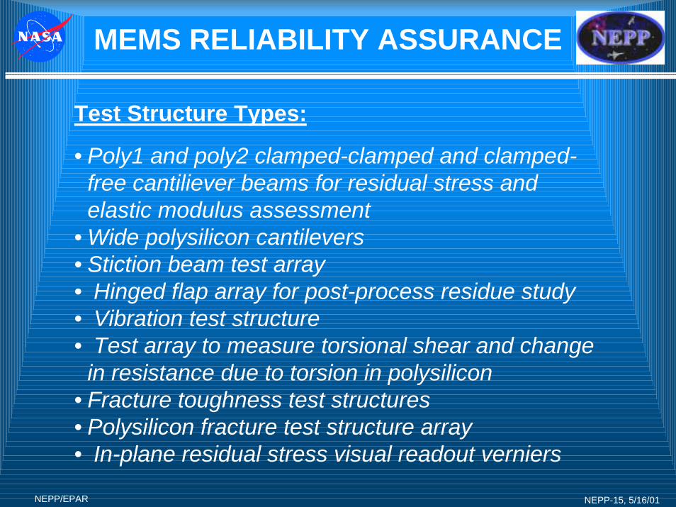
MEMS RELIABILITY ASSURANCE
• Poly1 and poly2 clamped-clamped and clamped-free cantiliever beams for residual stress andelastic modulus assessment
• Wide polysilicon cantilevers• Stiction beam test array• Hinged flap array for post-process residue study• Vibration test structure• Test array to measure torsional shear and change
in resistance due to torsion in polysilicon• Fracture toughness test structures• Polysilicon fracture test structure array• In-plane residual stress visual readout verniers
Test Structure Types:

NEPP-16, 5/16/01NEPP/EPAR
MEMS RELIABILITY ASSURANCE
•Fracture/failure mechanisms•Elastic modulus•Poisson's ratio•Fracture toughness•Electrical properties (migration, etc.)•Interfacial strength•Coefficient of thermal expansion (CTE)
3000X SEM image of fracturedunreleased cantilever beam array
damaged during dicing.
Material Properties:

NEPP-17, 5/16/01NEPP/EPAR
MEMS RELIABILITY ASSURANCE
•Residual stresses•Grain size•Stiction phenomena•Doping•Etching parameters•Surface roughness•Deposition methods,parameters•Post-process release etching•Post-process drying method(stiction)
High-resolution STEM image of oxide andpolysilicon layers deposited in MUMPS process.
Notice the clear definition of grain boundaries andinterfaces.
Process Feedback

NEPP-18, 5/16/01NEPP/EPAR
MEMS RELIABILITY ASSURANCE
SEM side view of a poly2 hinge afterpoly1 plate has been rotated 180°,
showing the ridge created by the dimpleclearly
SEM photo of a hinge without the dimplepatterned through it. While rotating thepoly1 plate, the hinge pin got pegged underthe poly2 staple. Any further rotation willbreak the pin. Also, rotation of the poly1plate is now irreversible.
Process Variations

NEPP-19, 5/16/01NEPP/EPAR
MEMS RELIABILITY ASSURANCE
•Storage, humidity effects•Radiation tolerance•Chemical exposure effects•Biocompatibility•Effects of extreme heat or cold•Effect of shock
AFM images of the top of a poly2 layer aftersacrificial layer removal for A MUMPs 37 chip.Scan size is 5µm X 5µm and height data scaleon the order of 40 nm.
Environmental Effects:

NEPP-20, 5/16/01NEPP/EPAR
MEMS RELIABILITY ASSURANCE
FUTURE PLANS:
•Complete testing and analysis on existing test structures•Expand library of test structures•Expand MEMS Reliability Alliance to include newprocesses•Include functional devices (not test structures) intoreliability framework