A Facts Device
131
A FACTS DEVICE: DISTRIBUTED POWER-FLOW CONTROLLER (DPFC) ABSTRACT This paper presents a new component within the flexible Ac- transmission system (FACTS) family, called distributed Power-flow controller (DPFC). The DPFC is derived from the unified Power- flow controller (UPFC). The DPFC can be considered as A UPFC with an eliminated common dc link. The active power exchange between the shunt and series converters, which is through the common dc link in the UPFC, is now through the transmission Lines at the third-harmonic frequency. The DPFC employs the distributed FACTS (D-FACTS) concept, which is to use multiple Small-size single- phase converters instead of the one large-size Three-phase series converter in the UPFC. The large number of Series converters provides redundancy, thereby increasing the system Reliability. As the D-FACTS converters are single-phase and Floating with respect to the ground, there is no high-voltage isolation required between the phases. Accordingly, the cost of the DPFC system is lower than the UPFC. The DPFC has the same Control capability as the UPFC, which comprises the adjustment of the line impedance, the transmission angle, and the bus voltage. The principle and analysis of the DPFC are presented in this paper and the corresponding experimental results that are carried out on a scaled prototype are also shown.
-
Upload
ruth-ruhama -
Category
Documents
-
view
7 -
download
0
description
This paper presents a new component within the flexible Ac-transmission system (FACTS) family, called distributed Power-flow controller (DPFC). The DPFC is derived from the unified Power-flow controller (UPFC).
Transcript of A Facts Device

A FACTS DEVICE: DISTRIBUTED POWER-FLOWCONTROLLER (DPFC)
ABSTRACT
This paper presents a new component within the flexible Ac-transmission system (FACTS)
family, called distributed Power-flow controller (DPFC). The DPFC is derived from the unified
Power-flow controller (UPFC). The DPFC can be considered as A UPFC with an eliminated
common dc link. The active power exchange between the shunt and series converters, which is
through the common dc link in the UPFC, is now through the transmission Lines at the third-
harmonic frequency. The DPFC employs the distributed FACTS (D-FACTS) concept, which is
to use multiple Small-size single-phase converters instead of the one large-size Three-phase
series converter in the UPFC. The large number of Series converters provides redundancy,
thereby increasing the system Reliability. As the D-FACTS converters are single-phase and
Floating with respect to the ground, there is no high-voltage isolation required between the
phases. Accordingly, the cost of the DPFC system is lower than the UPFC. The DPFC has the
same Control capability as the UPFC, which comprises the adjustment of the line impedance, the
transmission angle, and the bus voltage. The principle and analysis of the DPFC are presented in
this paper and the corresponding experimental results that are carried out on a scaled prototype
are also shown.
INTRODUCTION
THE growing demand and the aging of network smoke it desirable to control the power
flow in power-transmission systems fast and reliably. The flexible ac-transmission system
(FACTS) that is defined by IEEE as “a power-electronic based system and other static equipment
that provide control of one or more ac-transmission system parameters to enhance controllability
and increase power-transfer capability”, and can be utilized for power-flow control. Currently,
the unified power-flow controller (UPFC) shown in Fig. 1, is the most powerful FACTS device,
which can simultaneously control all the parameters of the system: the line impedance, the
transmission angle, and bus voltage.
Fig.1.Simplified representation of a UPFC.
The UPFC is the combination of a static synchronous compensator (STATCOM) and a
static synchronous series compensator (SSSC), which are coupled via a common dc link, to
allow bidirectional flow of active power between the series output terminals of the SSSC and the
shunt output terminals of the STATCOM. The converter in series with the line provides the main
function of the UPFC by injecting a four-quadrant voltage with controllable magnitude and
phase. The injected voltage essentially acts as a synchronous ac-voltage source, which is used to
vary the transmission angle and line impedance, thereby independently controlling the active and
reactive power flow through the line.
The series voltage results in active and reactive power injection or absorption between
the series converter and the transmission line. This reactive power is generated internally by the
series converter (see e.g., SSSC), and the active power is supplied by the shunt converter that is

back-to-back connected. The shunt converter controls the voltage of the dc capacitor by
absorbing or generating active power from the bus; therefore, it acts as a synchronous source in
parallel with the system. Similar to the STATCOM, the shunt converter can also provide reactive
compensation for the bus.
The components of the UPFC handle the voltages and currents with high rating;
therefore, the total cost of the system is high. Due to the common dc-link interconnection, a
failure that happens at one converter will influence the whole system. To achieve the required
reliability for power systems, bypass circuits and redundant backups (backup transformer, etc.)
are needed, which on other hand, increase the cost. Accordingly, the UPFC has not been
commercially used, even though; it has the most advanced control capabilities.
This paper introduces a new concept, called distributed power-flow controller (DPFC)
that is derived from the UPFC. The same as the UPFC, the DPFC is able to control all system
parameters. The DPFC eliminates the common dc link between the shunt and series converters.
The active power exchange between the shunt and the series converter is through the
transmission line at the third-harmonic frequency.
The series converter of the DPFC employs the distributed FACTS D-FACTS) concept.
Comparing with the UPFC, the DPFC have two major advantages: 1) low cost because of the
low-voltage isolation and the low component rating of the series converter and 2) high reliability
because of the redundancy of the series converters. This paper begins with presenting the
principle of the DPFC, followed by its steady-state analysis. After a short introduction of the
DPFC control, the paper ends with the experimental results of the DPFC.
POWER QUALITY
The contemporary container crane industry, like many other industry segments, is often
enamored by the bells and whistles, colorful diagnostic displays, high speed performance, and
levels of automation that can be achieved. Although these features and their indirectly related
computer based enhancements are key issues to an efficient terminal operation, we must not
forget the foundation upon which we are building. Power quality is the mortar which bonds the
foundation blocks. Power quality also affects terminal operating economics, crane reliability, our
environment, and initial investment in power distribution systems to support new crane
installations. To quote the utility company newsletter which accompanied the last monthly issue
of my home utility billing: ‘Using electricity wisely is a good environmental and business
practice which saves you money, reduces emissions from generating plants, and conserves our
natural resources.’ As we are all aware, container crane performance requirements continue to
increase at an astounding rate. Next generation container cranes, already in the bidding process,
will require average power demands of 1500 to 2000 kW – almost double the total average
demand three years ago. The rapid increase in power demand levels, an increase in container
crane population, SCR converter crane drive retrofits and the large AC and DC drives needed to
power and control these cranes will increase awareness of the power quality issue in the very
near future.
POWER QUALITY PROBLEMS
For the purpose of this article, we shall define power quality problems as:
‘Any power problem that results in failure or misoperation of customer equipment, manifests
itself as an economic burden to the user, or produces negative impacts on the environment.’
When applied to the container crane industry, the power issues which degrade power quality
include:
• Power Factor
• Harmonic Distortion
• Voltage Transients
• Voltage Sags or Dips• Voltage Swells
The AC and DC variable speed drives utilized on board container cranes are significant
contributors to total harmonic current and voltage distortion. Whereas SCR phase control creates
the desirable average power factor, DC SCR drives operate at less than this. In addition, line
notching occurs when SCR’s commutate, creating transient peak recovery voltages that can be 3
to 4 times the nominal line voltage depending upon the system impedance and the size of the
drives. The frequency and severity of these power system disturbances varies with the speed of
the drive. Harmonic current injection by AC and DC drives will be highest when the drives are
operating at slow speeds. Power factor will be lowest when DC drives are operating at slow
speeds or during initial acceleration and deceleration periods, increasing to its maximum value

when the SCR’s are phased on to produce rated or base speed. Above base speed, the power
factor essentially remains constant. Unfortunately, container cranes can spend considerable time
at low speeds as the operator attempts to spot and land containers. Poor power factor places a
greater kVA demand burden on the utility or engine-alternator power source. Low power factor
loads can also affect the voltage stability which can ultimately result in detrimental effects on the
life of sensitive electronic equipment or even intermittent malfunction. Voltage transients created
by DC drive SCR line notching, AC drive voltage chopping, and high frequency harmonic
voltages and currents are all significant sources of noise and disturbance to sensitive electronic
equipment.
It has been our experience that end users often do not associate power quality problems with
Container cranes, either because they are totally unaware of such issues or there was no
economic Consequence if power quality was not addressed. Before the advent of solid-state
power supplies, Power factor was reasonable, and harmonic current injection was minimal. Not
until the crane Population multiplied, power demands per crane increased, and static power
conversion became the way of life, did power quality issues begin to emerge. Even as harmonic
distortion and power Factor issues surfaced, no one was really prepared.
Even today, crane builders and electrical drive System vendors avoid the issue during
competitive bidding for new cranes. Rather than focus on Awareness and understanding of the
potential issues, the power quality issue is intentionally or unintentionally ignored. Power quality
problem solutions are available. Although the solutions are not free, in most cases, they do
represent a good return on investment. However, if power quality is not specified, it most likely
will not be delivered.
Power quality can be improved through:
• Power factor correction,
• Harmonic filtering,
• Special line notch filtering,
• Transient voltage surge suppression,
• Proper earthing systems.

In most cases, the person specifying and/or buying a container crane may not be fully aware of
the potential power quality issues. If this article accomplishes nothing else, we would hope to
Provide that awareness.
In many cases, those involved with specification and procurement of container cranes may not be
cognizant of such issues, do not pay the utility billings, or consider it someone else’s concern. As
a result, container crane specifications may not include definitive power quality criteria such as
power factor correction and/or harmonic filtering. Also, many of those specifications which do
Require power quality equipment do not properly define the criteria. Early in the process of
preparing the crane specification:
• Consult with the utility company to determine regulatory or contract requirements that must be
satisfied, if any.
• Consult with the electrical drive suppliers and determine the power quality profiles that can be
expected based on the drive sizes and technologies proposed for the specific project.
• Evaluate the economics of power quality correction not only on the present situation, but
consider the impact of future utility deregulation and the future development plans for the
terminal
THE BENEFITS OF POWER QUALITY
Power quality in the container terminal environment impacts the economics of the
terminal operation, affects reliability of the terminal equipment, and affects other consumers
served by the same utility service. Each of these concerns is explored in the following
paragraphs.
1. Economic Impact
The economic impact of power quality is the foremost incentive to container terminal operators.
Economic impact can be significant and manifest itself in several ways:
a. Power Factor Penalties
Many utility companies invoke penalties for low power factor on monthly billings. There
is no industry standard followed by utility companies. Methods of metering and calculating
power factor penalties vary from one utility company to the next. Some utility companies

actually meter kVAR usage and establish a fixed rate times the number of kVAR-hours
consumed. Other utility companies monitor kVAR demands and calculate power factor. If the
power factor falls below a fixed limit value over a demand period, a penalty is billed in the form
of an adjustment to the peak demand charges.
A number of utility companies servicing container terminal equipment do not yet invoke
power factor penalties. However, their service contract with the Port may still require that a
minimum power factor over a defined demand period be met. The utility company may not
continuously monitor power factor or kVAR usage and reflect them in the monthly utility
billings; however, they do reserve the right to monitor the Port service at any time. If the power
factor criteria set forth in the service contract are not met, the user may be penalized, or required
to take corrective actions at the user’s expense.
One utility company, which supplies power service to several east coast container
terminals in the USA, does not reflect power factor penalties in their monthly billings, however,
their service contract with the terminal reads as follows:
‘The average power factor under operating conditions of customer’s load at the point where
service is metered shall be not less than 85%. If below 85%, the customer may be required to
furnish, install and maintain at its expense corrective apparatus which will increase the
Power factor of the entire installation to not less than 85%. The customer shall ensure that no
excessive harmonics or transients are introduced on to the [utility] system. This may require
special power conditioning equipment or filters.
The Port or terminal operations personnel, who are responsible for maintaining container
cranes, or specifying new container crane equipment, should be aware of these requirements.
Utility deregulation will most likely force utilities to enforce requirements such as the example
above.
Terminal operators who do not deal with penalty issues today may be faced with some rather
severe penalties in the future. A sound, future terminal growth plan should include contingencies
for addressing the possible economic impact of utility deregulation.
b. System Losses
Harmonic currents and low power factor created by nonlinear loads, not only result in
possible power factor penalties, but also increase the power losses in the distribution system.
These losses are not visible as a separate item on your monthly utility billing, but you pay for

them each month. Container cranes are significant contributors to harmonic currents and low
power factor. Based on the typical demands of today’s high speed container cranes, correction of
power factor alone on a typical state of the art quay crane can result in a reduction of system
losses that converts to a 6 to 10% reduction in the monthly utility billing. For most of the larger
terminals, this is a significant annual saving in the cost of operation.
C. Power Service Initial Capital Investments
The power distribution system design and installation for new terminals, as well as
modification of systems for terminal capacity upgrades, involves high cost, specialized, high and
medium voltage equipment.
Transformers, switchgear, feeder cables, cable reel trailing cables, collector bars, etc.
must be sized based on the kVA demand. Thus cost of the equipment is directly related to the
total kVA demand. As the relationship above indicates, kVA demand is inversely proportional to
the overall power factor, i.e. a lower power factor demands higher kVA for the same kW load.
Container cranes are one of the most significant users of power in the terminal. Since container
cranes with DC, 6 pulse, SCR drives operate at relatively low power factor, the total kVA
demand is significantly larger than would be the case if power factor correction equipment were
supplied on board each crane or at some common bus location in the terminal. In the absence of
power quality corrective equipment, transformers are larger, switchgear current ratings must be
higher, feeder cable copper sizes are larger, collector system and cable reel cables must be larger,
etc.
Consequently, the cost of the initial power distribution system equipment for a system
which does not address power quality will most likely be higher than the same system which
includes power quality equipment.
2. Equipment Reliability

Poor power quality can affect machine or equipment reliability and reduce the life of
components. Harmonics, voltage transients, and voltage system sags and swells are all power
quality problems and are all interdependent.
Harmonics affect power factor, voltage transients can induce harmonics, the same
phenomena which create harmonic current injection in DC SCR variable speed drives are
responsible for poor power factor, and dynamically varying power factor of the same drives can
create voltage sags and swells. The effects of harmonic distortion, harmonic currents, and line
notch ringing can be mitigated using specially designed filters.
3. Power System Adequacy
When considering the installation of additional cranes to an existing power distribution
system, a power system analysis should be completed to determine the adequacy of the system to
support additional crane loads. Power quality corrective actions may be dictated due to
inadequacy of existing power distribution systems to which new or relocated cranes are to be
connected. In other words, addition of power quality equipment may render a workable scenario
on an existing power distribution system, which would otherwise be inadequate to support
additional cranes without high risk of problems.
4. Environment
No issue might be as important as the effect of power quality on our environment.
Reduction in system losses and lower demands equate to a reduction in the consumption of our
natural nm resources and reduction in power plant emissions. It is our responsibility as occupants
of this planet to encourage conservation of our natural resources and support measures which
improve our air quality.

FACTS
Flexible AC Transmission Systems, called FACTS, got in the recent years a well known
term for higher controllability in power systems by means of power electronic devices. Several
FACTS-devices have been introduced for various applications worldwide. A number of new
types of devices are in the stage of being introduced in practice.
In most of the applications the controllability is used to avoid cost intensive or landscape
requiring extensions of power systems, for instance like upgrades or additions of substations and
power lines. FACTS-devices provide a better adaptation to varying operational conditions and
improve the usage of existing installations. The basic applications of FACTS-devices are:
• Power flow control,
• Increase of transmission capability,
• Voltage control,
• Reactive power compensation,
• Stability improvement,
• Power quality improvement,
• Power conditioning,
• Flicker mitigation,
• Interconnection of renewable and distributed generation and storages.
Figure 1.1 shows the basic idea of FACTS for transmission systems. The usage of lines
for active power transmission should be ideally up to the thermal limits. Voltage and stability
limits shall be shifted with the means of the several different FACTS devices. It can be seen that
with growing line length, the opportunity for FACTS devices gets more and more important.
The influence of FACTS-devices is achieved through switched or controlled shunt
compensation, series compensation or phase shift control. The devices work electrically as fast
current, voltage or impedance controllers. The power electronic allows very short reaction times
down to far below one second.
The development of FACTS-devices has started with the growing capabilities of power
electronic components. Devices for high power levels have been made available in converters for
high and even highest voltage levels. The overall starting points are network elements
influencing the reactive power or the impedance of a part of the power system. Figure 1.2 shows
a number of basic devices separated into the conventional ones and the FACTS-devices.

For the FACTS side the taxonomy in terms of 'dynamic' and 'static' needs some
explanation. The term 'dynamic' is used to express the fast controllability of FACTS-devices
provided by the power electronics. This is one of the main differentiation factors from the
conventional devices. The term 'static' means that the devices have no moving parts like
mechanical switches to perform the dynamic controllability. Therefore most of the FACTS-
devices can equally be static and dynamic.
The left column in Figure 1.2 contains the conventional devices build out of fixed or
mechanically switch able components like resistance, inductance or capacitance together with
transformers. The FACTS-devices contain these elements as well but use additional power
electronic valves or converters to switch the elements in smaller steps or with switching patterns
within a cycle of the alternating current. The left column of FACTS-devices uses Thyristor
valves or converters. These valves or converters are well known since several years. They have
low losses because of their low switching frequency of once a cycle in the converters or the
usage of the Thyristors to simply bridge impedances in the valves.
The right column of FACTS-devices contains more advanced technology of voltage
source converters based today mainly on Insulated Gate Bipolar Transistors (IGBT) or Insulated
Gate Commutated Thyristors (IGCT). Voltage Source Converters provide a free controllable
voltage in magnitude and phase due to a pulse width modulation of the IGBTs or IGCTs.
High modulation frequencies allow to get low harmonics in the output signal and even to
compensate disturbances coming from the network. The disadvantage is that with an increasing
switching frequency, the losses are increasing as well. Therefore special designs of the
converters are required to compensate this.
Configurations of FACTS-Devices:
Shunt Devices:
The most used FACTS-device is the SVC or the version with Voltage Source Converter
called STATCOM. These shunt devices are operating as reactive power compensators. The main
applications in transmission, distribution and industrial networks are:
• Reduction of unwanted reactive power flows and therefore reduced network losses.
• Keeping of contractual power exchanges with balanced reactive power.
• Compensation of consumers and improvement of power quality especially with huge demand
fluctuations like industrial machines, metal melting plants, railway or underground train systems.
• Compensation of Thyristor converters e.g. in conventional HVDC lines.
• Improvement of static or transient stability.

Almost half of the SVC and more than half of the STATCOMs are used for industrial
applications. Industry as well as commercial and domestic groups of users require power quality.
Flickering lamps are no longer accepted, nor are interruptions of industrial processes due to
insufficient power quality. Railway or underground systems with huge load variations require
SVCs or STATCOMs.
SVC:
Electrical loads both generate and absorb reactive power. Since the transmitted load
varies considerably from one hour to another, the reactive power balance in a grid varies as well.
The result can be unacceptable voltage amplitude variations or even a voltage depression, at the
extreme a voltage collapse.
A rapidly operating Static Var Compensator (SVC) can continuously provide the reactive
power required to control dynamic voltage oscillations under various system conditions and
thereby improve the power system transmission and distribution stability.
Applications of the SVC systems in transmission systems:
a. To increase active power transfer capacity and transient stability margin
b. To damp power oscillations
c. To achieve effective voltage control
In addition, SVCs are also used

1. in transmission systems
A. To reduce temporary over voltages
B. To damp sub synchronous resonances
C. To damp power oscillations in interconnected power systems
2. in traction systems
a. To balance loads
b. To improve power factor
c. To improve voltage regulation
3. In HVDC systems
a. To provide reactive power to ac–dc converters
4. In arc furnaces
a. To reduce voltage variations and associated light flicker
Installing an SVC at one or more suitable points in the network can increase transfer capability
and reduce losses while maintaining a smooth voltage profile under different network conditions.
In addition an SVC can mitigate active power oscillations through voltage amplitude modulation.

SVC installations consist of a number of building blocks. The most important is the
Thyristor valve, i.e. stack assemblies of series connected anti-parallel Thyristors to provide
controllability. Air core reactors and high voltage AC capacitors are the reactive power elements
used together with the Thyristor valves. The step up connection of this equipment to the
transmission voltage is achieved through a power transformer.
SVC building blocks and voltage / current characteristic
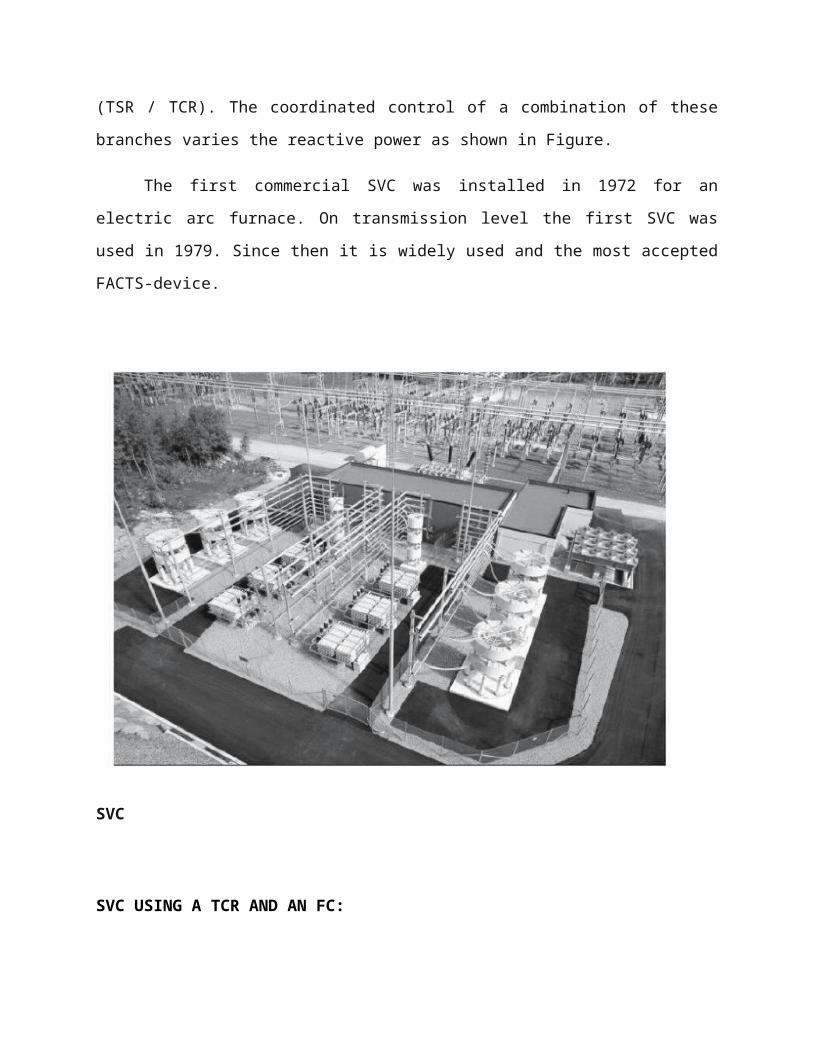
In principle the SVC consists of Thyristor Switched Capacitors (TSC) and Thyristor
Switched or Controlled Reactors (TSR / TCR). The coordinated control of a combination of
these branches varies the reactive power as shown in Figure.
The first commercial SVC was installed in 1972 for an electric arc furnace. On
transmission level the first SVC was used in 1979. Since then it is widely used and the most
accepted FACTS-device.

SVC
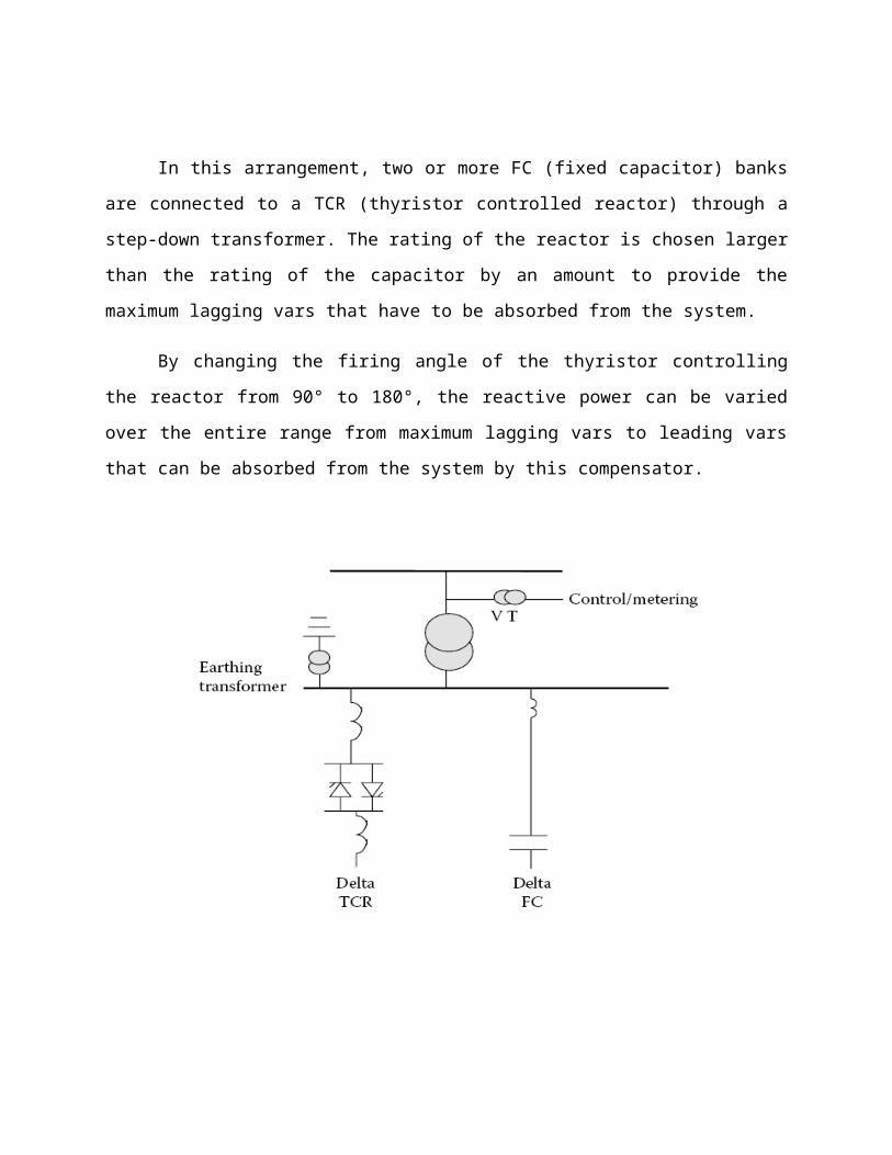
SVC USING A TCR AND AN FC:
In this arrangement, two or more FC (fixed capacitor) banks are connected to a TCR
(thyristor controlled reactor) through a step-down transformer. The rating of the reactor is chosen
larger than the rating of the capacitor by an amount to provide the maximum lagging vars that
have to be absorbed from the system.
By changing the firing angle of the thyristor controlling the reactor from 90° to 180°, the
reactive power can be varied over the entire range from maximum lagging vars to leading vars
that can be absorbed from the system by this compensator.

SVC of the FC/TCR type:
The main disadvantage of this configuration is the significant harmonics that will be
generated because of the partial conduction of the large reactor under normal sinusoidal steady-
state operating condition when the SVC is absorbing zero MVAr.
These harmonics are filtered in the following manner. Triplex harmonics are canceled by
arranging the TCR and the secondary windings of the step-down transformer in delta connection.
The capacitor banks with the help of series reactors are tuned to filter fifth, seventh, and
other higher-order harmonics as a high-pass filter. Further losses are high due to the circulating
current between the reactor and capacitor banks.

Comparison of the loss characteristics of TSC–TCR, TCR–FC compensators and
synchronous condenser
These SVCs do not have a short-time overload capability because the reactors are usually
of the air-core type. In applications requiring overload capability, TCR must be designed for
short-time overloading, or separate thyristor-switched overload reactors must be employed.
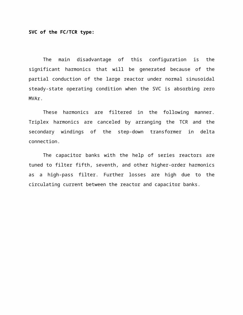
SVC USING A TCR AND TSC:
This compensator overcomes two major shortcomings of the earlier compensators by
reducing losses under operating conditions and better performance under large system
disturbances. In view of the smaller rating of each capacitor bank, the rating of the reactor bank
will be 1/n times the maximum output of the SVC, thus reducing the harmonics generated by the
reactor. In those situations where harmonics have to be reduced further, a small amount of FCs
tuned as filters may be connected in parallel with the TCR.

SVC of combined TSC and TCR type
When large disturbances occur in a power system due to load rejection, there is a
possibility for large voltage transients because of oscillatory interaction between system and the
SVC capacitor bank or the parallel. The LC circuit of the SVC in the FC compensator. In the
TSC–TCR scheme, due to the flexibility of rapid switching of capacitor banks without
appreciable disturbance to the power system, oscillations can be avoided, and hence the
transients in the system can also be avoided. The capital cost of this SVC is higher than that of
the earlier one due to the increased number of capacitor switches and increased control
complexity.
STATCOM:
In 1999 the first SVC with Voltage Source Converter called STATCOM (Static
Compensator) went into operation. The STATCOM has a characteristic similar to the
synchronous condenser, but as an electronic device it has no inertia and is superior to the
synchronous condenser in several ways, such as better dynamics, a lower investment cost and
lower operating and maintenance costs. A STATCOM is build with Thyristors with turn-off
capability like GTO or today IGCT or with more and more IGBTs. The static line between the
current limitations has a certain steepness determining the control characteristic for the voltage.
The advantage of a STATCOM is that the reactive power provision is independent from
the actual voltage on the connection point. This can be seen in the diagram for the maximum
currents being independent of the voltage in comparison to the SVC. This means, that even
during most severe contingencies, the STATCOM keeps its full capability.
In the distributed energy sector the usage of Voltage Source Converters for grid
interconnection is common practice today. The next step in STATCOM development is the
combination with energy storages on the DC-side.
The performance for power quality and balanced network operation can be improved
much more with the combination of active and reactive power.

STATCOM structure and voltage / current characteristic
STATCOMs are based on Voltage Sourced Converter (VSC) topology and utilize either
Gate-Turn-off Thyristors (GTO) or Isolated Gate Bipolar Transistors (IGBT) devices. The
STATCOM is a very fast acting, electronic equivalent of a synchronous condenser. If the
STATCOM voltage, Vs, (which is proportional to the dc bus voltage VC) is larger than bus
voltage, Es, then leading or capacitive VARS are produced. If Vs is smaller then Es then lagging
or inductive VARS are produced.

6 Pulses STATCOM
The three phases STATCOM makes use of the fact that on a three phase, fundamental
frequency, steady state basis, and the instantaneous power entering a purely reactive device must
be zero. The reactive power in each phase is supplied by circulating the instantaneous real power
between the phases. This is achieved by firing the GTO/diode switches in a manner that
maintains the phase difference between the ac bus voltage ES and the STATCOM generated
voltage VS. Ideally it is possible to construct a device based on circulating instantaneous power
which has no energy storage device (i.e. no dc capacitor).
A practical STATCOM requires some amount of energy storage to accommodate
harmonic power and ac system unbalances, when the instantaneous real power is non-zero. The
maximum energy storage required for the STATCOM is much less than for a TCR/TSC type of
SVC compensator of comparable rating.
STATCOM Equivalent Circuit
Several different control techniques can be used for the firing control of the STATCOM.
Fundamental switching of the GTO/diode once per cycle can be used. This approach will
minimize switching losses, but will generally utilize more complex transformer topologies.
As an alternative, Pulse Width Modulated (PWM) techniques, which turn on and off the
GTO or IGBT switch more than once per cycle, can be used. This approach allows for simpler
transformer topologies at the expense of higher switching losses.
The 6 Pulse STATCOM using fundamental switching will of course produce the 6 N1
harmonics. There are a variety of methods to decrease the harmonics. These methods include the
basic 12 pulse configuration with parallel star / delta transformer connections, a complete
elimination of 5th and 7th harmonic current using series connection of star/star and star/delta
transformers and a quasi 12 pulse method with a single star-star transformer, and two secondary
windings, using control of firing angle to produce a 30 phase shift between the two 6 pulse
bridges. This method can be extended to produce a 24 pulse and a 48 pulse STATCOM, thus
eliminating harmonics even further. Another possible approach for harmonic cancellation is a
multi-level configuration which allows for more than one switching element per level and
therefore more than one switching in each bridge arm. The ac voltage derived has a staircase
effect, dependent on the number of levels. This staircase voltage can be controlled to eliminate
harmonics.
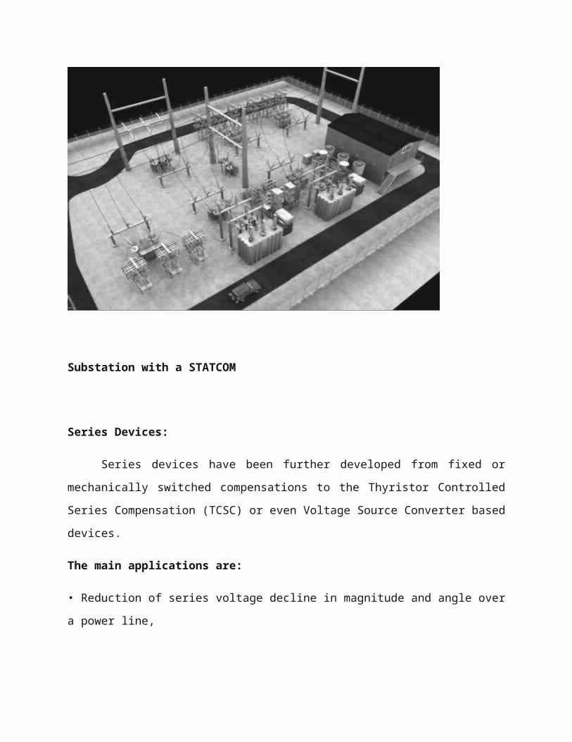
Substation with a STATCOM
Series Devices:
Series devices have been further developed from fixed or mechanically switched
compensations to the Thyristor Controlled Series Compensation (TCSC) or even Voltage Source
Converter based devices.
The main applications are:
• Reduction of series voltage decline in magnitude and angle over a power line,
• Reduction of voltage fluctuations within defined limits during changing power transmissions,
• Improvement of system damping resp. damping of oscillations,
• Limitation of short circuit currents in networks or substations,
• Avoidance of loop flows resp. power flow adjustments.
TCSC:
Thyristor Controlled Series Capacitors (TCSC) addresses specific dynamical problems in
transmission systems. Firstly it increases damping when large electrical systems are
interconnected. Secondly it can overcome the problem of Sub Synchronous Resonance (SSR), a
phenomenon that involves an interaction between large thermal generating units and series
compensated transmission systems.
The TCSC's high speed switching capability provides a mechanism for controlling line
power flow, which permits increased loading of existing transmission lines, and allows for rapid
readjustment of line power flow in response to various contingencies. The TCSC also can
regulate steady-state power flow within its rating limits.
From a principal technology point of view, the TCSC resembles the conventional series
capacitor. All the power equipment is located on an isolated steel platform, including the
Thyristor valve that is used to control the behavior of the main capacitor bank. Likewise the
control and protection is located on ground potential together with other auxiliary systems.
Figure shows the principle setup of a TCSC and its operational diagram. The firing angle and the
thermal limits of the Thyristors determine the boundaries of the operational diagram.

Advantages
Continuous control of desired compensation level
Direct smooth control of power flow within the network
Improved capacitor bank protection
Local mitigation of sub synchronous resonance (SSR). This permits higher levels of
compensation in networks where interactions with turbine-generator torsional vibrations
or with other control or measuring systems are of concern.
Damping of electromechanical (0.5-2 Hz) power oscillations which often arise between
areas in a large interconnected power network. These oscillations are due to the dynamics
of inter area power transfer and often exhibit poor damping when the aggregate power
tranfer over a corridor is high relative to the transmission strength.
Shunt and Series Devices
Dynamic Power Flow Controller
A new device in the area of power flow control is the Dynamic Power Flow Controller
(DFC). The DFC is a hybrid device between a Phase Shifting Transformer (PST) and switched
series compensation.
A functional single line diagram of the Dynamic Flow Controller is shown in Figure 1.19.
The Dynamic Flow Controller consists of the following components:
• A standard phase shifting transformer with tap-changer (PST)
• Series-connected Thyristor Switched Capacitors and Reactors
(TSC / TSR)
• A mechanically switched shunt capacitor (MSC). (This is
Optimal depending on the system reactive power requirements)
Based on the system requirements, a DFC might consist of a number of series TSC or
TSR. The mechanically switched shunt capacitor (MSC) will provide voltage support in case of
overload and other conditions. Normally the reactance of reactors and the capacitors are selected
based on a binary basis to result in a desired stepped reactance variation. If a higher power flow
resolution is needed, a reactance equivalent to the half of the smallest one can be added.
The switching of series reactors occurs at zero current to avoid any harmonics. However,
in general, the principle of phase-angle control used in TCSC can be applied for a continuous
control as well. The operation of a DFC is based on the following rules:
• TSC / TSR are switched when a fast response is required.
• The relieve of overload and work in stressed situations is handled by the TSC / TSR.

• The switching of the PST tap-changer should be minimized particularly for the currents higher
than normal loading.
• The total reactive power consumption of the device can be optimized by the operation of the
MSC, tap changer and the switched capacities and reactors.
In order to visualize the steady state operating range of the DFC, we assume an
inductance in parallel representing parallel transmission paths. The overall control objective in
steady state would be to control the distribution of power flow between the branch with the DFC
and the parallel path. This control is accomplished by control of the injected series voltage.
The PST (assuming a quadrature booster) will inject a voltage in quadrature with the
node voltage. The controllable reactance will inject a voltage in quadrature with the throughput
current. Assuming that the power flow has a load factor close to one, the two parts of the series
voltage will be close to collinear. However, in terms of speed of control, influence on reactive
power balance and effectiveness at high/low loading the two parts of the series voltage has quite
different characteristics.
The steady state control range for loadings up to rated current is illustrated in Figure 1.20,
where the x-axis corresponds to the throughput current and the y-axis corresponds to the injected
series voltage.

Fig1.20. Operational diagram of a DFC
Operation in the first and third quadrants corresponds to reduction of power through the
DFC, whereas operation in the second and fourth quadrants corresponds to increasing the power
flow through the DFC. The slope of the line passing through the origin (at which the tap is at
zero and TSC / TSR are bypassed) depends on the short circuit reactance of the PST.
Starting at rated current (2 kA) the short circuit reactance by itself provides an injected
voltage (approximately 20 kV in this case). If more inductance is switched in and/or the tap is
increased, the series voltage increases and the current through the DFC decreases (and the flow
on parallel branches increases). The operating point moves along lines parallel to the arrows in
the figure. The slope of these arrows depends on the size of the parallel reactance.
The maximum series voltage in the first quadrant is obtained when all inductive steps are
switched in and the tap is at its maximum.
Now, assuming maximum tap and inductance, if the throughput current decreases (due
e.g. to changing loading of the system) the series voltage will decrease.

At zero current, it will not matter whether the TSC / TSR steps are in or out, they will not
contribute to the series voltage. Consequently, the series voltage at zero current corresponds to
rated PST series voltage. Next, moving into the second quadrant, the operating range will be
limited by the line corresponding to maximum tap and the capacitive step being switched in (and
the inductive steps by-passed). In this case, the capacitive step is approximately as large as the
short circuit reactance of the PST, giving an almost constant maximum voltage in the second
quadrant.
Unified Power Flow Controller:
The UPFC is a combination of a static compensator and static series compensation. It acts
as a shunt compensating and a phase shifting device simultaneously.
Fig1.21. Principle configuration of an UPFC
The UPFC consists of a shunt and a series transformer, which are connected via two
voltage source converters with a common DC-capacitor.
The DC-circuit allows the active power exchange between shunt and series transformer to
control the phase shift of the series voltage. This setup, as shown in Figure 1.21, provides the full
controllability for voltage and power flow.

The series converter needs to be protected with a Thyristor bridge. Due to the high efforts
for the Voltage Source Converters and the protection, an UPFC is getting quite expensive, which
limits the practical applications where the voltage and power flow control is required
simultaneously.
OPERATING PRINCIPLE OF UPFC
The basic components of the UPFC are two voltage source inverters (VSIs) sharing a
common dc storage capacitor, and connected to the power system through coupling transformers.
One VSI is connected to in shunt to the transmission system via a shunt transformer, while the
other one is connected in series through a series transformer.
A basic UPFC functional scheme is shown in fig.1
s

The series inverter is controlled to inject a symmetrical three phase voltage system (Vse),
of controllable magnitude and phase angle in series with the line to control active and reactive
power flows on the transmission line. So, this inverter will exchange active and reactive power
with the line. The reactive power is electronically provided by the series inverter, and the active
power is transmitted to the dc terminals. The shunt inverter is operated in such a way as to
demand this dc terminal power (positive or negative) from the line keeping the voltage across the
storage capacitor Vdc constant. So, the net real power absorbed from the line by the UPFC is
equal only to the losses of the inverters and their transformers. The remaining capacity of the
shunt inverter can be used to exchange reactive power with the line so to provide a voltage
regulation at the connection point.
The two VSI’s can work independently of each other by separating the dc side. So in that
case, the shunt inverter is operating as a STATCOM that generates or absorbs reactive power to
regulate the voltage magnitude at the connection point. Instead, the series inverter is operating as
SSSC that generates or absorbs reactive power to regulate the current flow, and hence the power
low on the transmission line.
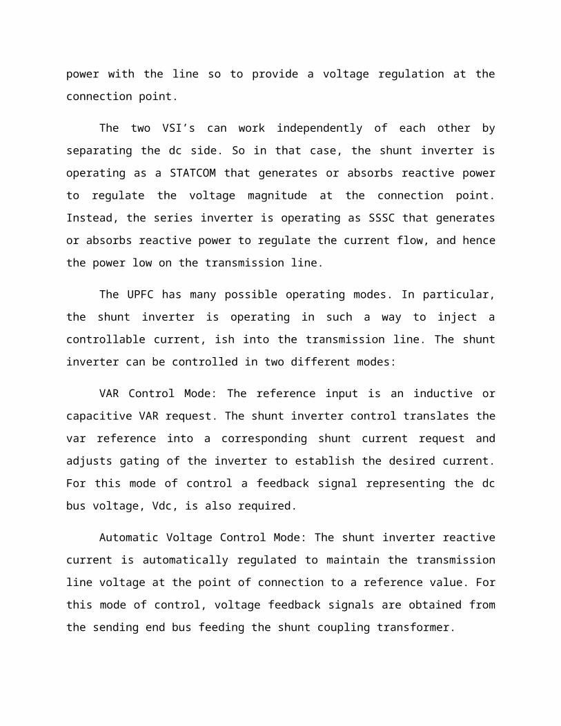
The UPFC has many possible operating modes. In particular, the shunt inverter is
operating in such a way to inject a controllable current, ish into the transmission line. The shunt
inverter can be controlled in two different modes:
VAR Control Mode: The reference input is an inductive or capacitive VAR request. The
shunt inverter control translates the var reference into a corresponding shunt current request and
adjusts gating of the inverter to establish the desired current. For this mode of control a feedback
signal representing the dc bus voltage, Vdc, is also required.
Automatic Voltage Control Mode: The shunt inverter reactive current is automatically
regulated to maintain the transmission line voltage at the point of connection to a reference
value. For this mode of control, voltage feedback signals are obtained from the sending end bus
feeding the shunt coupling transformer.
The series inverter controls the magnitude and angle of the voltage injected in series with
the line to influence the power flow on the line. The actual value of the injected voltage can be
obtained in several ways.
Direct Voltage Injection Mode: The reference inputs are directly the magnitude and phase
angle of the series voltage.
Phase Angle Shifter Emulation mode: The reference input is phase displacement between
the sending end voltage and the receiving end voltage. Line Impedance Emulation mode: The
reference input is an impedance value to insert in series with the line impedance
Automatic Power Flow Control Mode: The reference inputs are values of P and Q to
maintain on the transmission line despite system changes.
UNIFIED POWER FLOW CONTROLLER (UPFC)
Gyugyi proposed the Unified Power Flow Controller (UPFC) concept in 1991. The
UPFC was devised for the real time control and dynamic compensation of ac transmission
systems, providing multifunctional flexibility required to solve many of the problems facing the
delivery industry. Within the framework of traditional power transmission concepts, the UPFC
is able to control, simultaneously or selectively, all the parameters affecting power flow in the
transmission line (i.e., voltage, impedence and phase angle), and this unique capability is signed
by the adjective “unified” in its name. Alternatively, it can independently control both the real
and reactive power flows in the line.
Circuit Arrangement:
In the presently used practical implementation, The UPFC consists of two switching
converters, which in the implementations considered are voltage source inverters using gate turn-
off (GTO) thyristor valves, as illustrated in the Fig 2.1. These back to back converters labeled
“Inverter 1 and “Inverter 2” in the figure, are operated from a common dc link provided by a dc
storage capacitor.

This arrangement functions as an ac to ac power converter in which the real power can
freely flow in either direction between the ac terminals of the two inverters and each inverter can
independently generate (or absorb) reactive power at its own ac output terminal.
Fig. Basic circuit arrangement of unified power flow controller
OPERATION OF UPFC
Inverter 2 provides the main function of the UPFC by injecting an ac voltage Vpq with
controllable magnitude Vpq (0≤Vpq≤Vpqmax) and phase angle (0≤≤360), at the power frequency,
in series with the line via an insertion transformer. The injected voltage is considered essentially
as a synchronous voltage source. The transmission line current flows through this voltage source
resulting in real and reactive power exchange between it and the ac system. The real power
exchanged at the ac terminal (i.e., at the terminal of insertion transformer) is converted by the
inverter into dc power that appears at the dc link as positive or negative real power demanded.
The reactive power exchanged at the ac terminal is generated internally by the inverter.
The basic function of inverter 1 is to supply or absorb the real power demanded by
Inverter 2 at the common dc link. This dc link power is converted back to ac and coupled to the
transmission line via a shunt-connected transformer. Inverter 1 can also generate or absorb
controllable reactive power, if it is desired, and there by it can provide independent shunt
reactive compensation for the line.

It is important to note that where as there is a closed “direct” path for the real power
negotiated by the action of series voltage injection through Inverters 1 and 2 back to the line, the
corresponding reactive power exchanged is supplied or absorbed locally by inverter 2 and
therefore it does not flow through the line.
Thus, Inverter 1 can be operated at a unity power factor or be controlled to have a
reactive power exchange with the line independently of the reactive power exchanged by the
Inverter 2. This means there is no continuous reactive power flow through UPFC.
Basic Control Functions
Operation of the UPFC from the standpoint of conventional power transmission
based on reactive shunt compensation, series compensation, and phase shifting, the UPFC can
fulfill these functions and thereby meet multiple control objectives by adding the injected voltage
Vpq, with appropriate amplitude.

And phase angle, to the terminal voltage Vo. Using phasor representation, the basic UPFC power
flow control functions are illustrated in Fig 2.2.

Terminal Voltage Regulation, similar to that obtainable with a transformer tap-changer having
infinitely small steps, as shown at (a) where Vpq=V (boldface letters represent phasors) is
injected in-phase (or anti-phase) with Vo.
Series capacitor compensation is shown at (b) where Vpq=Vc is in quadrature with the line
current I.
Transmission angle Regulation (phase shifting) is shown at (c) where Vpq=Vo is injected with
angular relationship with respect to Vo that achieves the desired s phase shift (advance or retard)
without any change in magnitude.
Multifunctional Power Flow Control, executed by simultaneous terminal voltage regulation,
series capacitive compensation, and phase shifting, is shown at (d) where Vpq=V+Vc+Vo.
Basic Principles of P and Q Control
Consider Fig 2.3. At (a) a simple two machine (or two bus ac inter-tie) system with sending end
voltage Vs, receiving-end voltage Vr, and line (or tie) impedance X (assumed, for simplicity,
inductive) is shown. At (b) the voltages of the system in the form of a phasor diagram are shown
with transmission angle and Vs=Vr=V. At (c) the transmitted power P (P=V2/X sin) and the
reactive power Q=Qs=Qr (Q=V2/X (1-cos)) supplied at the ends of the line are shown plotted
against angle . At (d) the reactive power Q=Qs=Qr is shown plotted against the transmitted
power corresponding to “stable values of ” (i.e., 0<= <=90o).
Basic power system of fig2.3 with the well known transmission characteristics is introduced for
the purpose of providing a vehicle to establish the capability of the UPFC to control the
transmitted real power P and the reactive power demands, Qs and Qr, at the sending end,
respectively, the receiving end of the line.
Consider Fig 2.4, the simple power system of Fig 2.3 is expanded to include the UPFC. The
UPFC is represented by a controllable voltage source in series with the line which, as explained
in the previous section, can generate or absorb reactive power that it, or absorbed from it, bye the
sending end generator. The UPFC in series with the line is represented by the phasor Vpq having
magnitude Vpq(0 ≤ Vpq ≤ Vpqmax ) and angle ρ (0 ≤ ρ ≤ 360) measured from the given phase
position of phasor Vs, as illustrated in the figure. The line current represented by the phasor I,
flows through the series voltage source, Vpq and generally results in both reactive and real power
exchange. In order to represent UPFC properly, the series voltage source is stipulated to generate
only the reactive power Qpq it exchanges with the line. Thus the real power Ppq it negotiates with
the line is assumed to be transferred to the sending-end generator excited.

This is in arrangement with the UPFC circuit structure in which the dc link between the
two constituent inverters establish a bi-directional coupling for real power flow between the
injected series voltage source and the sending end bus.
As Fig 2.4 implies, in the present discussion it is further assumed for clarity that the shunt
reactive compensation capability of the UPFC not utilized. This is the UPFC shunt inverter is
assumed to be operated at unity power factor, its sole function being to transfer the real power
demand of the series inverter to the sending-end generator. With these assumptions, the series
voltage source, together with the real power coupling to the sending end generator as shown in
fig 2.4, is a an accurate representation of the basic UPFC.
It can be observed in Fig 2.4 that the transmission line “sees” Vs+Vpq as the effective
sending end voltage. Thus it is clear that the UPFC effects the voltage (both its magnitude and
angle) across the transmission line and therefore it is reasonable to expect that it is able to
control, by varying the magnitude and angle of Vpq, the transmittable real power as well as the
reactive power demand of the line at any given transmission angle between the sending-end and
receiving-end voltages.

INDEPENDENT REAL AND REACTIVE POWER FLOW CONTROL
In Fig2.5(a) through 2.5(b) the reactive power Qs supplied by the sending-end generator,
and Qr supplied by the receiving-end generator, are shown plotted separately against the
transmitted power ρ as a function of the magnitude Vpq and angle p of the injected voltage
phasor Vpq at four transmission lines; δ=0,30,60 and 90. At Vpq=0 each of these plots becomes a
discrete point on the basic Q-p curve as shown in Fig 2.3(d), which is included in each of the
above figures for refernce.
The curves showing the relationships between Qs and P, and Qr and P, for the
transmission angle range of 0<= δ<=90, when the UPFC is operated to provide the maximum
transmittable power with no reactive power control (Vpq=Vpqmax and ρ= ρp=Pmax), are also shown
by a broken –line with the label “P (δ) =MAX” at the sending end and respectively, “receiving-
end” plots of the figure.
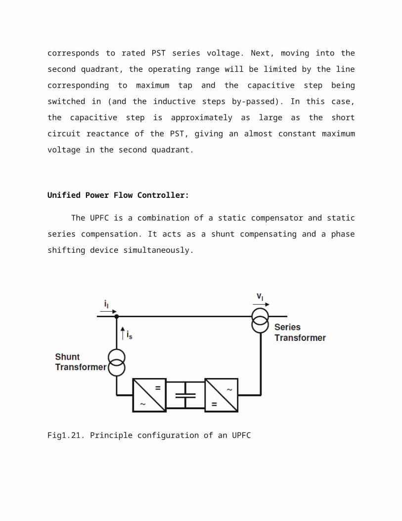
Fig 2.5(a)&2.5(b). Attainable sending-end reactive power Vs transmitted power
(left hand side plots) and receiving-end reactive power Vs transmitted power (right
hand side plots ) values with the UPFC at =0o and =30o

Fig 2.5(c) & 2.5(d). Attainable sending-end reactive power Vs transmitted power (left-hand
side plots) and receiving-end reactive power Vs transmitted power (right hand side plots)
values with the UPFC at =60o and =90o
Consider the first fig.5 (a), which illustrates the case when the transmission angle is zero(δ=0).
With Vpq=0, P, Qs and Qr are all zero, i.e., the system is standstill at the origins of the Qs, P and
Qr, P coordinates. The circle around the origin of the {Q s, P} and {Qr, P} planes sown the
variation of Qs and P and Qr and P respectively. As the voltage phasor Vpq, with its maximum
Vpqmax is rotated a full revolution (0<= ρ<=360). The area within these circles defines all P and Q
values obtainable by controlling the magnitude Vpq and ρ of the phasor Vpq.

In other words, the circle in {Qs,p} and {Qr,p} planes define all P and Qs and
respectively, P and Qr values attainable with the UPFC of a given rating. It can be observed, for
example, that the UPFC with the stipulated voltage rating of 0.5. P.u. is able to establish 0.5. P.u.
power flow, in either direction, without imposing any reactive power demand on either the
sending-end or the receiving-end generator. Of course, the UPFC, as seen, can force the
generator at one end to supply reactilve power for the generator at the other end. (In case of
inertia, one system can be forced to supply reactive power of the line.)
In general at any given transmission angle δ, the transmitted real power P, and the
reactive power demands at the transmission line ends, Qs and Qr, can be controlled freely by the
UPFC with in the boundaries obtained in the {Qs,p}and {Qr,P} planes by rotating the injected
voltage phasor Vpq with its maximum magnitude a full revolution. The boundary in each plane is
centered around the point defined by the transmission angle on the Q verses P curve that
characterisis the basic power transmission at Vpq=0.
Consider the next case of δ=30 (fig. 5(b)), it is seen that the receiving-end control region
boundary in the {Qs, P} plane become an ellipse. As the transmission angle δ is further
increased, for example, to 60 (fig.5(c)), the ellipse defining the control region for P and Qs in the
{Qs, P} plane becomes narrower and finally 90(fig. 5(d)) it degerates into a straight line. By
contrast, the control region boundary for p and Qr in the {Qr,P} plane remains a circle at all
transmission angles.
DISTRIBUTED POWER FLOW CONTROLLER
INTRODUCTION
IN the previous chapter, an overview was given of mechanical- and PE-based PFCDs. Because
of high control capability, the PE-based combined PFCs, specifically UPFC and IPFC are
suitable for the future power system. However, the UPFC and IPFC are not widely applied in
practice, due to their high cost and the susceptibility to failures. Generally, the reliability can be
improved by reducing the number of components; however, this is not possible due to the
complex topology of the UPFC and IPFC. To reduce the failure rate of the components by
selecting components with higher ratings than necessary or employing redundancy at the
component or system levels are also options. Unfortunately, these solutions increase the initial
investment necessary, negating any cost- related advantages. Accordingly, new approaches are
needed in order to increase reliability and reduce cost of the UPFC and IPFC at the same time.
After studying the failure mode of the combined FACTS devices, it is found that a common DC
link between converters reduces the reliability of a device, because a failure in one converter will
pervade the whole device though the DC link. By eliminating this DC link, the converters within
the FACTS devices are operated independently, thereby increasing their reliability. The
elimination of the common DC link also allows the DSSC to series converters. In that case, the
reliability of the new device is further improved due to the redundancy provided by the
distributed series converters. In addition, series Converter distribution reduces cost because no
high-voltage isolation and high power rating components are required at the series part. By
applying the two approaches –eliminating the common DC link and distributing the series
converter, the UPFC is further developed into a new combined FACTS device: the Distributed
Power Flow Controller (DPFC), as shown in Figure 3-1.

Figure 3-1: Flowchart from UPFC to DPFC
In this chapter, the principle of the DPFC is presented, followed by a steady-state analysis of the
DPFC. During the analysis, the control capability and the influence of the DPFC on the network
are investigated. The principle and analysis of another device that emerges from the IPFC, the
so-called Distributed Interline Power Flow Controller (DIPFC), is also introduced.
DISTRIBUTED POWER FLOW CONTROLLER (DPFC)
In this section, DPFC topology and operating principle are introduced.
DPFC TOPOLOGY:
By introducing the two approaches outlined in the previous section (elimination of the
common DC link and distribution of the series converter) into the UPFC, the DPFC is achieved.
Similar as the UPFC, the DPFC consists of shunt and series connected converters. The shunt
converter is similar as a STATCOM, while the series converter employs the DSSC concept,
which is to use multiple single-phase converters instead of one three-phase converter. Each
converter within the DPFC is independent and has its own DC capacitor to provide the required
DC voltage. The configuration of the DPFC is shown in Figure 3-2.

Figure 3-2: DPFC configuration
As shown, besides the key components - shunt and series converters, a DPFC also requires a
high pass filter that is shunt connected to the other side of the transmission line and a
transformer on each side of the line. The reason for these extra components will be explained
later. The unique control capability of the UPFC is given by the back-to-back connection
between the shunt and series converters, which allows the active power to freely exchange. To
ensure the DPFC has the same control capability as the UPFC, a method that allows active power
exchange between converters with an eliminated DC link is required.
DPFC OPERATING PRINCIPLE
ACTIVE POWER EXCHANGE WITH ELIMINATED DC LINK
Within the DPFC, the transmission line presents a common connection between the AC
ports of the shunt and the series converters. Therefore, it is possible to exchange active power
through the AC ports. The method is based on power theory of non-sinusoidal components.
According to the Fourier analysis, non-sinusoidal voltage and current can be expressed as the
sum of sinusoidal functions in different frequencies with different amplitudes. The active power
resulting from this non-sinusoidal voltage and current is defined as the mean value of the product
of voltage and current. Since the integrals of all the cross product of terms with different
frequencies are zero, the active power can be expressed by:

where Vi and Ii are the voltage and current at the ith harmonic frequency respectively, and is
the corresponding angle between the voltage and current. Equation (3.1) shows that the active
powers at different frequencies are independent from each other and the voltage or current at one
frequency has no influence on the active power at other frequencies. The independence of the
active power at different frequencies gives the possibility that a converter without a power source
can generate active power at one frequency and absorb this power from other frequencies.
By applying this method to the DPFC, the shunt converter can absorb active
power from the grid at the fundamental frequency and inject the power back at a harmonic
frequency. This harmonic active power flows through a transmission line equipped with series
converters. According to the amount of required active power at the fundamental frequency, the
DPFC series converters generate a voltage at the harmonic frequency, there by absorbing the
active power from harmonic components. Neglecting losses, the active power generated at the
fundamental frequency is equal to the power absorbed at the harmonic frequency. For a better
understanding, Figure 3-3 indicates how the active power is exchanged between the shunt and
the series converters in the DPFC system. The high-pass filter within the DPFC blocks the
fundamental frequency components and allows the harmonic components to pass, thereby
providing a return path for the
harmonic components. The shunt and series converters, the high pass filter and the ground form
a closed loop for the harmonic current.
USING THIRD HARMONIC COMPONENTS
Due to the unique features of 3rd harmonic frequency components in a three-phase system,
the 3rd harmonic is selected for active power exchange in the DPFC. In a three-phase

DISTRIBUTED POWER FLOW CONTROLLER
Figure 3-3: Active power exchange between DPFC converters
System, the 3rd harmonic in each phase is identical, which means they are ‘zero-sequence’
components. Because the zero-sequence harmonic can be naturally blocked by trans-
formers and these are widely incorporated in power systems (as a means of changing voltage),
there is no extra filter required to prevent harmonic leakage. As introduced above, a high-pass
filter is required to make a closed loop for the harmonic current and the cutoff frequency of this
filter is approximately the fundamental frequency.
Because the voltage isolation is high and the harmonic frequency is close to the cutoff
frequency, the filter will be costly. By using the zero-sequence harmonic, the costly filter can be
replaced by a cable that connects the neutral point of the transformer on the right side in
Figure 3-2 with the ground. Because the -winding appears open-circuit to the 3rd harmonic
current, all harmonic current will flow through the Y- winding and concentrate to the grounding
cable as shown in Figure 3-4. Therefore, the large high-pass filter is eliminated.

Figure 3-4: Utilize grounded transformer to filter zero-sequence harmonic
Another advantage of using the 3rd harmonic to exchange active power is that the grounding of
the transformers can be used to route the harmonic current in a meshed network. If the
network requires the harmonic current to flow through a specific branch, the neutral point of the
transformer in that branch, at the side opposite to the shunt converter, will be grounded and
vice versa. Figure 3-5 shows a simple example of routing the harmonic current by using the
grounding of the transformer. Because the floating neutral point is located on the
transformer of the line without the series converter, it is an open-circuit for 3rd harmonic
components and therefore no 3rd harmonic current will flow through this line.
Figure 3-5: Route the harmonic current by using the grounding of the transformer

The harmonic at the frequencies like 3rd, 6th, 9th... are all zero-sequence and all can be
used to exchange active power in the DPFC. However, the 3rd harmonic is selected, because it is
the lowest frequency among all zero-sequence harmonics. The relationship between the
exchanged active power at the ith harmonic frequency Pi and the voltages generated by the
converters is expressed by the well known the power flow equation and given as:
Where Xi is the line impedance at ith frequency, and are the voltage magnitudes
of the harmonic of the shunt and series converters, and is the angle difference
between the two voltages. As shown, the impedance of the line limits the active power exchange
capacity. To exchange the same amount of active power, the line with high impedance requires
higher voltages. Because the transmission line impedance is mostly inductive and proportional to
frequency, high transmission frequencies will cause high impedance and result in high voltage
within converters. Consequently, the zero-sequence harmonic with the lowest frequency - the 3rd
harmonic - has been selected.
DPFC CONTROL
To control multiple converters, a DPFC consists of three types of controllers: central control,
shunt control and series control, as shown in Figure 3-6.

Figure 3-6: DPFC control block diagram
The shunt and series control are localized controllers and are responsible for maintaining their
own converters’ parameters. The central control takes care of the DPFC functions at the power
system level. The function of each controller is listed:
• Central control: The central control generates the reference signals for both the shunt and
series converters of the DPFC. Its control function depends on the specifics of the DPFC
application at the power system level, such as power flow control, low frequency power
oscillation damping and balancing of asymmetrical components. According to the system
requirements, the central control gives corresponding voltage reference signals for the series
converters and reactive current signal for the shunt converter. All the reference signals generated
by the central control concern the fundamental frequency components.
• Series control: Each series converter has its own series control. The controller is used to
maintain the capacitor DC voltage of its own converter, by using 3rd harmonic frequency
components, in addition to generating series voltage at the fundamental frequency as required by
the central control.
• Shunt control: The objective of the shunt control is to inject a constant 3 rd harmonic current
into the line to supply active power for the series converters. At the same time, it maintains the
capacitor DC voltage of the shunt converter at a constant value by absorbing active power from
the grid at the fundamental frequency and injecting the required reactive current at the
fundamental frequency into the grid.
The detailed schematics and designs of the DPFC control will be introduced in following chapters.
VARIATION OF THE SHUNT CONVERTER
In the DPFC, the shunt converter should be a relatively large three-phase converter
that generates the voltage at the fundamental and 3rd harmonic frequency simultaneously. A
conventional choice would be a three-leg, three-wire converter. However, the converter is an
open circuit for the 3rd harmonic components and is therefore incapable of generating a 3rd
harmonic component. Because of this, the shunt converter in a DPFC will require a different type
of 3-phase converter.
There are several 3-phase converter topologies that can generate 3rd harmonic frequency
components, such as multi-leg, multi-wire converters or three single-phase converters [July 99].
These solutions normally introduce more components, thereby increasing total cost.
A new topology for the DPFC shunt converter is proposed. The topology utilizes
the existing Y-_ transformer to inject the 3rd harmonic current into the grid. A single- phase
converter is connected between the transformer’s neutral point and the ground, and injects a 3rd
harmonic current into the neutral point of the transformer. This current evenly spreads into the 3-
phase line through the transformer. The converter can be powered by an additional back-to-back
converter connected to the low-voltage side of the transformer.
The circuit scheme of this topology is shown in Figure 3-7. For a symmetrical system, the
voltage potential at the neutral point and fundamental frequency is zero. Accordingly, the single-
phase converter only handles the 3rd harmonic voltages, which are much lower than the voltage
at the fundamental frequency. As the single-phase converter is only used to provide active power
for the series converter, the voltage and power rating are small. In addition, the single-phase
converter uses the already present transformer as a grid connection. The single-phase
converter is powered by another converter through a common DC link. In the case of the system
with a STATCOM, the single-phase converter can be directly connected back-to-back to the DC
side of the STATCOM, as shown in Figure 3-7.

Figure 3-7: DPFC shunt converter configuration
ADVANTAGES AND LIMITATION OF THE DPFC
The DPFC can be considered a UPFC that employs the D-FACTS concept and the concept of
exchanging power through the 3rd harmonic. In this way, the DPFC inherits all their advantages:
• High controllability: the DPFC can simultaneously control all the parameters of the
transmission network: line impedance, transmission angle and bus voltage.
• High reliability: the redundancy of the series converter gives high reliability without increasing
cost. In addition, the shunt and series converters are independent and failure of one will not
influence the other converters.
• Low cost: there is no phase-to-phase voltage isolation required between the series converters of
different phases.
The power rating of each converter is also low. Because of the large number of the series
converters, they can be manufactured in series production. If the power system is already
equipped with the STATCOM, the system can be updated to the DPFC with only low additional
costs. However, there is a drawback to using the DPFC:
• Extra currents: Because the exchange of power between the converters takes place through the
same transmission line as the main power, extra currents at the 3rd harmonic frequency are
introduced.

These currents reduce the capacity of the transmission line and result in extra losses
within the line and the two transformers. However, because this extra current is at the 3rd
harmonic frequency, the increase in the RMS value of the line current is not large and through
the design process can be limited to less than 5% of the nominal current.
Power Electronics
Power electronics have a widely spread range of applications from electrical machine
drives to excitation systems, industrial high current rectifiers for metal smelters, frequency
controllers or electrical trains. FACTS-devices are just one application beside others, but use the
same technology trends. It has started with the first Thyristor rectifiers in 1965 and goes to the
nowadays modularized IGBT or IGCT voltage source converters. Without repeating lectures in
Semiconductors or Converters, the following sections provide some basic information.
Semiconductors
Since the first development of a Thyristor by General Electric in 1957, the targets for
power semiconductors are low switching losses for high switching rates and minimal conduction
losses. The innovation in the FACTS area is mainly driven by these developments. Today, there
are Thyristor and Transistor technologies available. The below figure shows the ranges of power
and voltage for the applications of the specific semiconductors.
The Thyristor is a device, which can be triggered with a pulse at the gate and remains in the
on-stage until the next current zero crossing. Therefore only one switching per half-cycle is
possible, which limits the controllability.

Ranges of converter voltages and power of applications for power semiconductors
Thyristors have the highest current and blocking voltage. This means that fewer
semiconductors need to be used for an application. Thyristors are used as switches for capacities
or inductances, in converters for reactive power compensators or as protection switches for less
robust power converters. The Thyristors are still the devices for applications with the highest
voltage and power levels. They are part of the mostly used FACTS-devices up to the biggest
HVDC-Transmissions with a voltage level above 500 kV and power above 3000 MVA.
To increase the controllability, GTO-Thyristors have been developed, which can be switched
off with a voltage peak at the gate. These devices are nowadays replaced by Insulated Gate
Commutated Thyristors (IGCT), which combine the advantage of the Thyristor, the low on stage
losses, with low switching losses.
These semiconductors are used in smaller FACTS-devices and drive applications. The Insulated
Gate Bipolar Transistor (IGBT) is getting more and more importance in the FACTS area. An
IGBT can be switched on with a positive voltage and switched off with a zero voltage. This
allows a very simple gate drive unit to control the IGBT.

The voltage and power level of the applications is on the way to grow up to 300 kV and
1000 MVA for HVDC with Voltage Source Converters.
The IGBT capability covers nowadays the whole range of power system applications. An
important issue for power semiconductors is the packaging to ensure a reliable connection to the
gate drive unit. This electronic circuit ensures beside the control of the semiconductor as well its
supervision and protection. A development in the Thyristor area tries to trigger the Thyristor
with a light signal through an optical fiber. This allows the decoupling of the Semiconductor and
the gate drive unit. The advantage is that the electronic circuit can be taken out of the high
electromagnetic field close to the Thyristor. The disadvantage is, that the protection of the
Thyristor has to be implemented in the Thyristor itself, which leads to an extremely complex
component. A supervision of the Thyristor by the gate drive unit is as well impossible in this
case, which leads to disadvantages for the entire converter.
A second issue for the packing is the stacking of the semiconductor devices. A number of
devices need to be stacked to achieve the required voltage level for the power system application.
A mechanically stable packaging needs to ensure an equal current distribution in the
semiconductor. The below figure shows three examples of stacked IGCTs, Thyristors and
IGBTs.

Semiconductor stacks, a) Medium Voltage IGCT 3-level topology, 9 MVA power stack,
b) SVC Thyristor Valve c) High Voltage IGBT stack for STATCOM
As an example the IGBT packaging shall be explained in detail. In Figure below an IGBT
Press pack is shown. Each sub-module contains nine pins of which six are IGBT chips and three
are Diode chips. Between two and six sub-modules can be integrated in one frame. The pins are
designed to press the chip with a spring on an Aluminum plate. If the entire module is stacked,
the sub-modules with the pins are pressed into the frame until the frames are laying tight on each
other. With this a well-defined pressure is equally distributed throughout all chips.
Due to the enormous number of chips in power system converter, a single chip failure
shall not lead to a disturbance of the entire FACTS-device. In the case of a short circuit of a chip
it is melting together with the Aluminum plate providing a long-term stable short circuit of the
module. The converter is designed in a way that more modules are stacked than necessary, so
that between maintenance intervals a defined number can fail. All these developments in the
power semiconductor and its packaging area lead to reliable system setups today.
IGBT-Module (1 kArms, 2.5 kV) with four sub-modules for Voltage Source Converter
(+/-150kVDC, 300 MVA)

INSULATED GATE BIPOLAR TRANSISTOR (IGBT)
IGBT has been developed by combining into it the best qualities of both BJT and
PMOSFET. Thus an IGBT possesses high input impedance like a PMOSFET and has low on-
state power loss as in a BJT. Further, IGBT is free from second breakdown problem present in
BJT. All these merits have made IGBT very popular amongst power-electronics engineers. IGBT
is also known as metal oxide insulated gate transistor (MOSIGT), conductively-modulated field
effect transistor (COMFET) or gain-modulated FET (GEMFET). It was also initially called
insulated gate transistor (IGT).
The insulated-gate bipolar transistor or IGBT is a three-terminal power
semiconductor device, noted for high efficiency and fast switching. It switches electric power in
many modern appliances: electric cars, variable speed refrigerators, air-conditioners, and even
stereo systems with digital amplifiers. Since it is designed to rapidly turn on and off, amplifiers
that use it often synthesize complex waveforms with pulse width modulation and low-pass
filters.
The IGBT combines the simple gate-drive characteristics of the MOSFETs with the
high-current and low–saturation-voltage capability of bipolar transistors by combining an
isolated-gate FET for the control input, and a bipolar power transistor as a switch, in a single
device. The IGBT is used in medium- to high-power applications such as switched-mode power
supply, traction motor control and induction heating. Large IGBT modules typically consist of
many devices in parallel and can have very high current handling capabilities in the order of
hundreds of amps with blocking voltages of 6,000 V.
The IGBT is a fairly recent invention. The first-generation devices of the 1980s
and early 1990s were relatively slow in switching, and prone to failure through such modes as
latch up and secondary breakdown. Second-generation devices were much improved, and the
current third-generation ones are even better, with speed rivaling MOSFETs, and excellent
ruggedness and tolerance of over loads.

Basic Structure
Fig illustrates the basic structure of an IGBT. It is constructed virtually in the same manner as a
power MOSFET. There is , however , a major difference in the substrate. The n+ layer substrate
at the drain in a PMOSFET is now substituted in the IGBT by a p+ layer substrate called
collector C. Like a power MOSFET, an IGBT has also thousands of basic structure cell
connected approximately on a single chip of silicon.
In IGBT, p+ substrate is called injection layer because it injects holes into n -
layer. The n- layer is called drift region. As in other semiconductor devices, thickness of n - layer
determines the voltage blocking capability of IGBT. The p layer is called body of IGBT.The n -
layer in between p+ and p regions serves to accommodate the depletion layer of pn- junction , i.e.
junction J2.
N-Channel IGBT Cross Section
Equivalent Circuit
An examination of reveals that if we move vertically up from collector to
emitter. We come across p+, n- , p layer s. Thus, IGBT can be thought of as the combination of
MOSFET and p+ n- p layer s. Thus, IGBT can be thought of as the combination of MOSFET and
p+ n- p transistor Q1 .Here Rd is resistance offered by n – drift region. Approximate equivalent
circuit of an IGBT.

Exact equivalent circuit
The existence of another path from collector to emitter, this path is collector, p+, n-, p (n-
channel), n+ and emitter. There is, thus, another inherent transistor Q2 as n- pn+ in the structure
of IGBT. The interconnection between two transistors Q1 and Q2.This gives the complete
equivalent circuit of an IGBT. Here Rby is the existence offered by p region to flow of hole
current Ih .
The two transistor equivalent circuit illustrates that an IGBT structure has a
parasitic thyristor in it. Parasitic thyristor is shown in line.

Working
When collector is made positive with respect to emitter, IGBT gets forward biased.
With no voltage between gate and emitter, two junctions between n- region and p region (i.e.
junction J2) are reversed biased; so no current flows from collector to emitter
When gate is made positive with respect to emitter by voltage VG, with gate-emitter
voltage more than the threshold voltage VGET of IGBT, an n-channel or inversion layer, is formed
in the upper part of p region just beneath the gate, as in PMOSFET . This n- channel short
circuits the n- region with n+ emitter regions. Electrons from the n+ emitter begin to flow to n-
drift region through n-channel. As IGBT is forward biased with collector positive and emitter
negative, p+ collector region injects holes into n- drift region .In short; n-drift region is flooded
with electrons from p-body region and holes from p+ collector region. With this, the injection
carrier density in n- drift region increases considerably and as a result, conductivity of n- region
enhances significantly. Therefore, IGBT gets turned on and begins to conducts forward current
IC.
Current Ic, or Ie of two current components:
1. Holes current Ih due to injected holes flowing from collector ,p+ n- p transistor Q1, p-
body region resistance Rby and emitter .
2. Electronic current Ie due to injected electrons flowing from collector, or load, current
IC=emitter current Ie=Ih+Ie.
Major component of collector current is electronic current Ie, i.e. main current path for collector,
or load, current is through p+, n -, drift resistance Rd and n-channel resistance Rch. Therefore, the
voltage drop in IGBT in its on-state is
Vc e . o n = I c . R c h + I c . Rd + V j i
=voltage drop [in n - channel] + across drift in n- region + across forward
biased p+ n- junction J1.
Here Vji is usually 0.7 to 1v as in a p-n diode. The voltage drop Ic. Rch is due to n-channel
resistance, almost the same as in a PMOSFET.

The voltage drop Vdf = Ic.Rd in UGBT is much less than that in PMOSFET. It is due to
substantial increase in the conductivity caused by injection of electrons and holes in n- drift
region. The conductivity increase is the main reason for the low on-state voltage drop in IGBT
than that it is in PMOSFET.
Latch-up in IGBT
From the above that IGBT structure has two inherent transistors Q1 and Q2,
which constitute a parasitic thyristor. When IGBT is on, the whole current flows through
transistor p+ n- p and p- body resistance Rby. If load current Ic is large, hole component of
current Ih would also be large. This large current would increase the voltage drop Ih. Rby which
may forward bias the base p- emitter n+ junction of transistor Q2. As a consequence, parasitic
transistor Q2 gets turned on which further facilitates in the turn-on of parasitic transistor p+ n- p
labeled Q1. The parasitic thyristor, consisting of Q1 and Q2, eventually latches on through
regenerative action, when sum of their current gains α1+α2 reaches unity as in a conventional
thyristor .With parasitic thyristor on, IGBT latches up and after this, collector emitter current is
no longer under the control of gate terminal. The only way now to turn-off the latched up IGBT
is by forced commutation of current as is done in a conventional thyristor .If this latch up is not
aborted quickly, excessive power dissipation may destroy the IGBT. The latch up discussed here
occurs when the collector current Ice exceeds a certain critical value .the device manufactures
always specify the maximum permissible value of load current Ice that IGBT can handle without
latch up.
At present, several modifications in the fabrication techniques are listed in the
literatures which are used to avoid latch-up in IGBTs. As such, latch up free IGBTs are
available.
IGBT Characteristics
The circuit shows the various parameters pertaining to IGBT characteristics.
Static I-V or output characteristics of an IGBT (n-channel type) show the plot of collector
current Ic versus collector-emitter voltage Vce for various values of gate-emitter voltages VGE1,
VGE2 etc .These characteristics are shown below .In the forward direction, the shape of the
output characteristics is similar to that of BJT.
But here the controlling parameter is gate-emitter voltage VGE because IGBT
is a voltage controlled device. When the device is off, junctionJ2 blocks forward voltage and in
case reverse voltage appears across collector and emitter, junction J1 blocks it. Vrm is the
maximum reverse breakdown voltage.
The transfer characteristic of an IGBT is a plot of collector current Ic versus gate-
emitter voltage VGE .This characteristics is identical to that of power MOSFET. When VGE is
less than the threshold voltage VGET, IGBT is in the off state.
Static V-I characteristics
Switching Characteristics
Switching characteristics of an IGBT during turn-on and turn-off are sketched.
The turn-on time is defined as the time between by instance of forward blocking to forward on-
state. Turn-on time is composed of delay time tdn and rise time tr ,i.e. ton=tdn+tr. The delay time
is defined as the time for the collector-emitter voltage to fall from Vce to 0.9 Vce. Here Vce is
the initial collector-emitter voltage.Time tdn may also be defined as the time for the collector
current to rise from its initial leakage current Ice to 0.1 Ic. Here Ic is the final value of the
collector current.
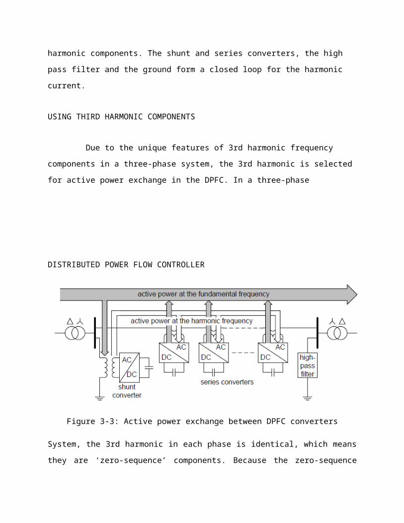
The rise time tr is the time during which collector-emitter falls from 0.9VCE to
0.1VCE. IT is also defined as the time for the collector current to rise from 0.1Ic to its final value
Ic.After time ton, the collector current Ic and the collector-emitter voltage falls to small value
called conduction drop=VCES where subscript s denotes saturated value.
The turn-off time is somewhat complex. It consists of three intervals
1. Delay time tdf
2. Initial fall time tf1
3. Final time tf2
i.e. toff=tdf+tf1+tf2
The delay time is the time during which gate voltage falls from VGE to threshold voltage
VGET.As VGE falls to VGET during tdf, the collector current falls from Ic to 0.9 Ic. At the end
of the tdf, collector-emitter voltage begins to rise. The first fall time Tf1 is defined as the time
during which collector current falls from 90 to 20 % of its initial value Ic, or the time during
which collector-emitter voltage rises from Vces to 0.1 Vce.
The final fall time tf2 is the time during which collector current falls from 20 to
10% of Ic, or the time during which collector-emitter voltage rises from 0.1 VCE to final value
VCE.
Applications of IGBTs
IGBTs are widely used in medium power applications such as AC and DC motor
drives, UPS systems, power supplies and drives for solenoids, relays and contactors. Though
IGBTs are somewhat more expensive than BJTs, yet they are becoming popular because of
lower gate-drive requirement, lower switching losses and smaller snubber circuit requirements.
IGBT converter are more efficient with less size as well as cost, as compared to converters based
on BJTs. Recently, IGBT inverter induction-motor drives using 15-20KHZ. Switching frequency
favour where audio-noise is objectionable. In most applications, IGBTs will eventually push out
BJTs. At present , the state of the art IGBTs of 1200vots, 500 Amps ratings , 0.25-20 µs turn off
time with operating frequency are available.
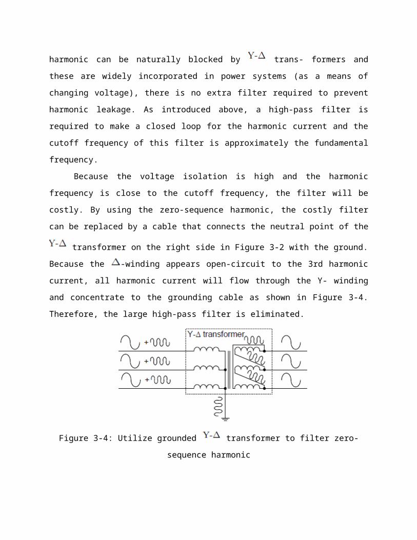
Comparison of IGBT with MOSFET
Relative merits and demerits of IGBT over PMOSFET are enumerated below.
1. In PMOSFET, the three terminals are called gate , source , drain where as the
corresponding terminal for the IGBTs are gate , emitter and collector.
2. Both IGBT and PMOSFET posses high input impedance.
3. Both are voltage control devices.
4. With rising temperature, increase in on-state resistance in PMOSFET is much
pronounced than in IGBT. So on state voltage drop and losses rise rapidely in
PMOSFET than IGBT , with rising temperature.
5. With rising
PULSE WIDTH MODULATION
What is PWM?
Pulse Width Modulation (PWM) is the most effective means to achieve constant voltage
battery charging by switching the solar system controller’s power devices. When in PWM
regulation, the current from the solar array tapers according to the battery’s condition and
recharging needs consider a waveform such as this: it is a voltage switching between 0v and 12v.
It is fairly obvious that, since the voltage is at 12v for exactly as long as it is at 0v, then a
'suitable device' connected to its output will see the average voltage and think it is being fed 6v -
exactly half of 12v. So by varying the width of the positive pulse - we can vary the 'average'
voltage.
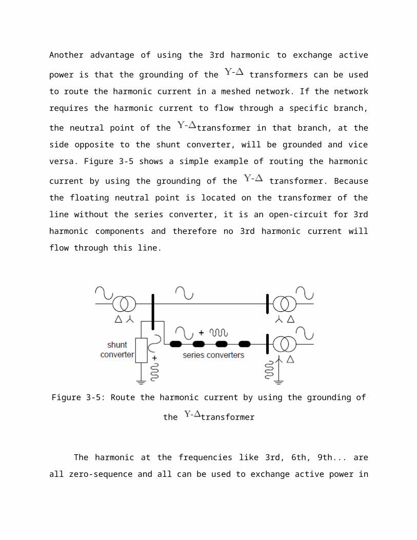
Similarly, if the switches keep the voltage at 12 for 3 times as long as at 0v, the average
will be 3/4 of 12v - or 9v, as shown below.
and if the output pulse of 12v lasts only 25% of the overall time, then the average is
By varying - or 'modulating' - the time that the output is at 12v (i.e. the width of the
positive pulse) we can alter the average voltage. So we are doing 'pulse width modulation'. I said
earlier that the output had to feed 'a suitable device'. A radio would not work from this: the radio
would see 12v then 0v, and would probably not work properly. However a device such as a
motor will respond to the average, so PWM is a natural for motor control.
Pulse Width modulator
So, how do we generate a PWM waveform? It's actually very easy, there are circuits
available in the TEC site. First you generate a triangle waveform as shown in the diagram below.
You compare this with a d.c voltage, which you adjust to control the ratio of on to off time that
you require. When the triangle is above the 'demand' voltage, the output goes high.

When the demand speed it in the middle (A) you get a 50:50 output, as in black. Half the
time the output is high and half the time it is low. Fortunately, there is an IC (Integrated circuit)
called a comparator: these come usually 4 sections in a single package. One can be used as the
oscillator to produce the triangular waveform and another to do the comparing, so a complete
oscillator and modulator can be done with half an IC and maybe 7 other bits.
The triangle waveform, which has approximately equal rise and fall slopes, is one of the
commonest used, but you can use a saw tooth (where the voltage falls quickly and rinses slowly).
You could use other waveforms and the exact linearity (how good the rise and fall are) is not too
important.
Traditional solenoid driver electronics rely on linear control, which is the application of a
constant voltage across a resistance to produce an output current that is directly proportional to
the voltage. Feedback can be used to achieve an output that matches exactly the control signal.
However, this scheme dissipates a lot of power as heat, and it is therefore very inefficient.
A more efficient technique employs pulse width modulation (PWM) to produce the
constant current through the coil. A PWM signal is not constant. Rather, the signal is on for part
of its period, and off for the rest. The duty cycle, D, refers to the percentage of the period for
which the signal is on.
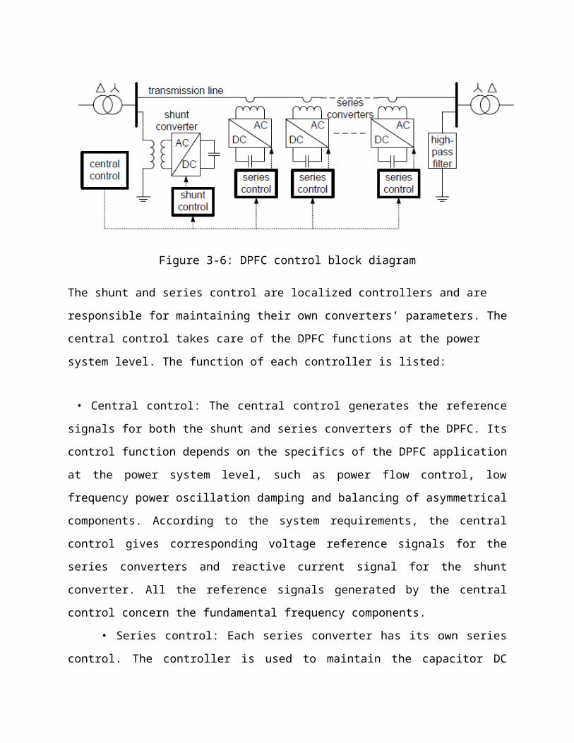
duty cycle can be anywhere from 0, the signal is always off, to 1, where the signal is
constantly on. A 50% D results in a perfect square wave. (Figure 1)
A solenoid is a length of wire wound in a coil. Because of this configuration, the solenoid
has, in addition to its resistance, R, a certain inductance, L. When a voltage, V, is applied across
an inductive element, the current, I, produced in that element does not jump up to its constant
value, but gradually rises to its maximum over a period of time called the rise time (Figure 2).
Conversely, I do not disappear instantaneously, even if V is removed abruptly, but decreases
back to zero in the same amount of time as the rise time.
Therefore, when a low frequency PWM voltage is applied across a solenoid, the current
through it will be increasing and decreasing as V turns on and off. If D is shorter than the rise
time, I will never achieve its maximum value, and will be discontinuous since it will go back to
zero during V’s off period.

In contrast, if D is larger than the rise time, I will never fall back to zero, so it will be
continuous, and have a DC average value. The current will not be constant, however, but will
have a ripple (Figure 4).
At high frequencies, V turns on and off very quickly, regardless of D, such that the
current does not have time to decrease very far before the voltage is turned back on. The
resulting current through the solenoid is therefore considered to be constant. By adjusting the D,
the amount of output current can be controlled. With a small D, the current will not have much
time to rise before the high frequency PWM voltage takes effect and the current stays constant.
With a large D, the current will be able to rise higher before it becomes constant.
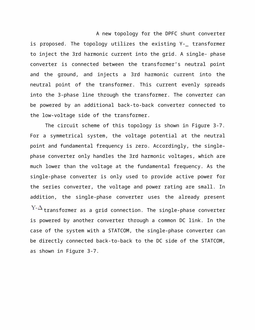
Dither
Static friction, stiction, and hysteresis can cause the control of a hydraulic valve to be
erratic and unpredictable. Stiction can prevent the valve spool from moving with small input
changes, and hysteresis can cause the shift to be different for the same input signal. In order to
counteract the effects of stiction and hysteresis, small vibrations about the desired position are
created in the spool. This constantly breaks the static friction ensuring that it will move even
with small input changes, and the effects of hysteresis are average out.
Dither is a small ripple in the solenoid current that causes the desired vibration and there
by increases the linearity of the valve. The amplitude and frequency of the dither must be
carefully chosen. The amplitude must be large enough and the frequency slow enough that the
spool will respond, yet they must also be small and fast enough not to result in a pulsating
output.
The optimum dither must be chosen such that the problems of stiction and hysteresis are
overcome without new problems being created. Dither in the output current is a byproduct of low
frequency PWM, as seen above. However, the frequency and amplitude of the dither will be a
function of the duty cycle, which is also used to set the output current level. This means that low
frequency dither is not independent of current magnitude. The advantage of using high frequency
PWM is that dither can be generated separately, and then superimposed on top of the output
current.
This allows the user to independently set the current magnitude (by adjusting the D), as
well as the dither frequency and amplitude. The optimum dither, as set by the user, will therefore
be constant at all current levels.
Why the PWM frequency is important:
The PWM is a large amplitude digital signal that swings from one voltage extreme to the
other. And, this wide voltage swing takes a lot of filtering to smooth out. When the PWM
frequency is close to the frequency of the waveform that you are generating, then any PWM
filter will also smooth out your generated waveform and drastically reduce its amplitude. So, a
good rule of thumb is to keep the PWM frequency much higher than the frequency of any
waveform you generate.
Finally, filtering pulses is not just about the pulse frequency but about the duty cycle and
how much energy is in the pulse. The same filter will do better on a low or high duty cycle pulse
compared to a 50% duty cycle pulse. Because the wider pulse has more time to integrate to a
stable filter voltage and the smaller pulse has less time to disturb it the inspiration was a request
to control the speed of a large positive displacement fuel pump. The pump was sized to allow full
power of a boosted engine in excess of 600 Hp.
At idle or highway cruise, this same engine needs far less fuel yet the pump still normally
supplies the same amount of fuel. As a result the fuel gets recycled back to the fuel tank,
unnecessarily heating the fuel. This PWM controller circuit is intended to run the pump at a low
speed setting during low power and allow full pump speed when needed at high engine power
levels.
Motor Speed Control (Power Control)
Typically when most of us think about controlling the speed of a DC motor we think of
varying the voltage to the motor. This is normally done with a variable resistor and provides a
limited useful range of operation. The operational range is limited for most applications
primarily because torque drops off faster than the voltage drops.

Most DC motors cannot effectively operate with a very low voltage. This method also
causes overheating of the coils and eventual failure of the motor if operated too slowly. Of
course, DC motors have had speed controllers based on varying voltage for years, but the range
of low speed operation had to stay above the failure zone described above.
Additionally, the controlling resistors are large and dissipate a large percentage of energy
in the form of heat. With the advent of solid state electronics in the 1950’s and 1960’s and this
technology becoming very affordable in the 1970’s & 80’s the use of pulse width modulation
(PWM) became much more practical. The basic concept is to keep the voltage at the full value
and simply vary the amount of time the voltage is applied to the motor windings. Most PWM
circuits use large transistors to simply allow power On & Off, like a very fast switch.
This sends a steady frequency of pulses into the motor windings. When full power is
needed one pulse ends just as the next pulse begins, 100% modulation. At lower power settings
the pulses are of shorter duration. When the pulse is On as long as it is Off, the motor is
operating at 50% modulation. Several advantages of PWM are efficiency, wider operational
range and longer lived motors. All of these advantages result from keeping the voltage at full
scale resulting in current being limited to a safe limit for the windings.
PWM allows a very linear response in motor torque even down to low PWM% without
causing damage to the motor. Most motor manufacturers recommend PWM control rather than
the older voltage control method. PWM controllers can be operated at a wide range of
frequencies. In theory very high frequencies (greater than 20 kHz) will be less efficient than
lower frequencies (as low as 100 Hz) because of switching losses.
The large transistors used for this On/Off activity have resistance when flowing current, a
loss that exists at any frequency. These transistors also have a loss every time they “turn on” and
every time they “turn off”. So at very high frequencies, the “turn on/off” losses become much
more significant. For our purposes the circuit as designed is running at 526 Hz. Somewhat of an
arbitrary frequency, it works fine.

Depending on the motor used, there can be a hum from the motor at lower PWM%. If
objectionable the frequency can be changed to a much higher frequency above our normal
hearing level (>20,000Hz) .
PWM Controller Features:
This controller offers a basic “Hi Speed” and “Low Speed” setting and has the option to
use a “Progressive” increase between Low and Hi speed. Low Speed is set with a trim pot inside
the controller box. Normally when installing the controller, this speed will be set depending on
the minimum speed/load needed for the motor. Normally the controller keeps the motor at this
Lo Speed except when Progressive is used and when Hi Speed is commanded (see below). Low
Speed can vary anywhere from 0% PWM to 100%.
Progressive control is commanded by a 0-5 volt input signal. This starts to increase PWM
% from the low speed setting as the 0-5 volt signal climbs. This signal can be generated from a
throttle position sensor, a Mass Air Flow sensor, a Manifold Absolute Pressure sensor or any
other way the user wants to create a 0-5 volt signal. This function could be set to increase fuel
pump power as turbo boost starts to climb (MAP sensor). Or, if controlling a water injection
pump, Low Speed could be set at zero PWM% and as the TPS signal climbs it could increase
PWM%, effectively increasing water flow to the engine as engine load increases. This controller
could even be used as a secondary injector driver (several injectors could be driven in a batch
mode, hi impedance only), with Progressive control (0-100%) you could control their output for
fuel or water with the 0-5 volt signal.
Progressive control adds enormous flexibility to the use of this controller. Hi Speed is
that same as hard wiring the motor to a steady 12 volt DC source. The controller is providing
100% PWM, steady 12 volt DC power. Hi Speed is selected three different ways on this
controller: 1) Hi Speed is automatically selected for about one second when power goes on. This
gives the motor full torque at the start. If needed this time can be increased ( the value of C1
would need to be increased). 2) High Speed can also be selected by applying 12 volts to the High
Speed signal wire. This gives Hi Speed regardless of the Progressive signal.

When the Progressive signal gets to approximately 4.5 volts, the circuit achieves 100%
PWM – Hi Speed.
How does this technology help?
The benefits noted above are technology driven. The more important question is how the PWM
Technology jumping from a 1970’s technology into the new millennium offers:
• Longer battery life:
– reducing the costs of the solar system
– reducing battery disposal problems
• More battery reserve capacity:
– increasing the reliability of the solar system
– reducing load disconnects
– opportunity to reduce battery size to lower
the system cost
• Greater user satisfaction:
– get more power when you need it for less money!!
MODELLING OF CASE STUDY
DPFC PRINCIPLE
Two approaches are applied to the UPFC to increase the reliability and to reduce the cost;
they are as follows. First, eliminating the common dc link of the UPFC and second distributing
the series converter, as shown in Fig. 2. By combining these two approaches, the new FACTS
device—DPFC is achieved.

Fig.2. Flowchart from UPFC to DPFC.
The DPFC consists of one shunt and several series-connected converters. The shunt
converter is similar as a STATCOM, while the series converter employs the D-FACTS concept,
which is to use multiple single-phase converters instead of one large rated converter. Each
converter within the DPFC is independent and has its own dc capacitor to provide the required dc
voltage. The configuration of the DPFC is shown in Fig. 3.
Fig.3. DPFC configuration.
As shown, besides the key components, namely the shunt and series converters, the
DPFC also requires a high-pass filter that is shunt connected at the other side of the transmission
line, and two Y–Δ transformers at each side of the line. The reason for these extra components
will be explained later. The unique control capability of the UPFC is given by the back-to-back
connection between the shunt and series converters, which allows the active power to exchange
freely. To ensure that the DPFC have the same control capability as the UPFC, a method that
allows the exchange of active power between converters with eliminated dc link is the
prerequisite.

A.ELIMINATE DC LINK
Within the DPFC, there is a common connection between the ac terminals of the shunt
and the series converters, which is the transmission line. Therefore, it is possible to exchange the
active power through the ac terminals of the converters. The method is based on the power
theory of non sinusoidal components. According to the Fourier analysis, a non sinusoidal voltage
and current can be expressed by the sum of sinusoidal functions in different frequencies with
different amplitudes. The active power resulting from this non sinusoidal voltage and current is
defined as the mean value of the product of voltage and current. Since the integrals of all the
cross product of terms with different frequencies are zero, the active power can be expressed by
..................... (1)
By applying this method to the DPFC, the shunt converter can absorb active power from
the grid at the fundamental frequency and inject the current back into the grid at a harmonic
frequency. This harmonic current will flow through the transmission line. According to the
amount of required active power at the fundamental frequency, the DPFC series converters
generate a voltage at the harmonic frequency, thereby absorbing the active power from harmonic
components. Assuming a lossless converter, the active power generated at fundamental
frequency is equal to the power absorbed from the harmonic frequency. For a better
understanding, Fig. 4 indicates how the active power exchanges between the shunt and the series
converters in the DPFC system.
Fig. 4. Active power exchange between DPFC converters.

The high-pass filter within the DPFC blocks the fundament frequency components and
allows the harmonic components to pass, thereby providing a return path for the harmonic
components. The shunt and series converters, the high-pass filter, and the ground form the closed
loop for the harmonic current.
Due to the unique characters of third-harmonic frequency components, the third harmonic
is selected to exchange the active power in the DPFC. In a three-phase system, the third
harmonic in each phase is identical, which is referred to as “zero-sequence.” The zero-sequence
harmonic can be naturally blocked by Y–Δ transformers, which are widely used in power system
to change voltage level. Therefore, there is no extra filter required to prevent the harmonic
leakage to the rest of the network. In addition, by using the third harmonic, the costly high-pass
filter, as shown in Fig. 4, can be replaced by a cable that is connected between the neutral point
of the Y–Δ transformer on the right side in Fig. 3 and the ground. Because the Δ winding appears
open circuit to the third-harmonic current, all harmonic current will flow through the Y-winding
and concentrate to the grounding cable, as shown in Fig. 5. Therefore, the large-size high-pass
filter is eliminated.
Fig.5.Utilize grounded Y–Δ transformer to provide the path for the zero sequencethird harmonic.
Another advantage of using third harmonic to exchange active Power is that the way of
grounding of Y–Δ transformers can Be used to route the harmonic current in a meshed network.
If The branch requires the harmonic current to flow through, the Neutral point of the Y–Δ
transformer at the other side in that Branch will be grounded and vice versa. Fig. 6 demonstrates
A simple example of routing the harmonic current by using a Grounding Y–Δ transformer.
Because the transformer of the Line without the series converter is floating, it is open circuit
third-harmonic components.

Therefore, no third-harmonic Current will flow through this line.
Fig.6.Route the harmonic current by using the grounding status of the Y–Δ transformer.Theoretically, the third-, sixth-, and ninth-harmonic frequencies are all zero-sequence,
and all can be used to exchange active power in the DPFC. As it is well known, the capacity of a
transmission line to deliver power depends on its impedance. Since the transmission-line
impedance is inductive and proportional to the frequency, high-transmission frequencies will
cause high impedance. Consequently, the zero-sequence harmonic with the lowest frequency—
third harmonic is selected.
B. DISTRIBUTED SERIES CONVERTER
The D-FACTS is a solution for the series-connected FACTS, Which can dramatically
reduce the total cost and increase the Reliability of the series FACTS device. The idea of the D-
FACTS Is to use a large number of controllers with low rating instead of One large rated
controller. The small controller is a single-phase Converter attached to transmission lines by a
single-turn transformer. The converters are hanging on the line so that no costly High-voltage
isolation is required. The single-turn transformer uses the transmission line as the secondary
winding, inserting Controllable impedance into the line directly. Each D-FACTS Module is self-
powered from the line and controlled remotely by wireless or power-line communication (see
Fig. 7).

Fig.7.D-FACTS unit configuration.
The structure of the D-FACTS results in low cost and high reliability. As D-FACTS units
are single-phase devices floating on Lines, high-voltage isolations between phases are avoided.
The Unit can easily be applied at any transmission-voltage level, because It does not require
supporting phase-ground isolation. The Power and voltage rating of each unit is relatively small.
Further, the units are clamped on transmission lines, and therefore, no Land is required. The
redundancy of the D-FACTS provides an uninterrupted operation during a single module failure,
thereby giving a much higher reliability than other FACTS devices.
DPFC Advantages
The DPFC can be considered as a UPFC that employs the DFACTS concept and the
concept of exchanging power through harmonic. Therefore, the DPFC inherits all the advantages
of the UPFC and the D-FACTS, which are as follows.
1) High control capability. The DPFC can simultaneously control all the parameters of the power
system: the line impedance, the transmission angle, and the bus voltage. The elimination of the
common dc link enables separated installation of the DPFC converters. The shunt and series
converters can be placed at the most effectively location. Due to the high control capability, the
DPFC can also be used to improve the power quality and system stability, such as low-frequency
power oscillation damping, voltage sag restoration, or balancing asymmetry.

2) High reliability. The redundancy of the series converter gives an improved reliability. In
addition, the shunt and series converters are independent, and the failure at one place will not
influence the other converters. When a failure occurs in the series converter, the converter will
be short-circuited by bypass protection, thereby having little influence to the network. In the case
of the shunt converter failure, the shunt converter will trip and the series converter will stop
providing active compensation and will act as the D-FACTS controller.
3) Low cost. There is no phase-to-phase voltage isolation required by the series converter. Also,
the power rating of each converter is small and can be easily produced in series production lines.
However, as the DPFC injects extra current at the third harmonic frequency into the transmission
line, additional losses in the transmission line and transformer should be aware of.
ANALYSIS OF THE DPFC
In this section, the steady-state behavior of the DPFC is analyzed, and the control
capability of the DPFC is expressed in the parameters of the network and the DPFC. To simplify
the DPFC, the converters are replaced by controllable voltage sources in series with impedance.
Since each converter generates the voltage at two different frequencies, it is represented by two
series-connected controllable voltage sources, one at the fundamental frequency and the other at
the third-harmonic frequency. Assuming that the converters and the transmission line are
lossless, the total active power generated by the two frequency voltage sources will be zero. The
multiple series converters are simplified as one large converter with the voltage, which is equal
to the sum of the voltages for all series converter, as shown in Fig. 8.
Fig.8.DPFC simplified representation.

In Fig. 8, the DPFC is placed in a two-bus system with the sending-end and the receiving-
end voltages Vs and Vr , respectively. The transmission line is represented by an inductance L
with the line current I. The voltage injected by all the DPFC series converters is Vse,1 and Vse,3
at the fundamental and the third-harmonic frequency, respectively. The shunt converter is
connected to the sending bus through the inductor Lsh and generates the voltage Vsh,1 and
Vsh,3 ; the current injected by the shunt converter is Ish . The active and reactive power flow at
the receiving end is Pr and Qr, respectively.
This representation consists of both the fundamental and third-harmonic frequency
components. Based on the superposition theorem, the circuit in Fig. 8 can be further simplified
by being split into two circuits at different frequencies. The two circuits are isolated from each
other, and the link between these circuits is the active power balance of each converter, as shown
in Fig. 9.
Fig.9.DPFC equivalent circuit. (a) Fundamental frequency. (b) Third harmonic frequency.
The power-flow control capability of the DPFC can be illustrated by the active power Pr
and reactive power Qr received at the receiving end. Because the DPFC circuit at the
fundamental frequency behaves the same as the UPFC, the active and reactive power flow can be
expressed as follows (1)
……………….. (2)
Where Pr0 ,Qr0 , and θ are the active, reactive power flow, and the transmission angle of
the uncompensated system,Xse,1 = ωLse is the line impedance at fundamental frequency, and |V|
is the voltage magnitude at both ends.

In the PQ-plane, the locus of the power flow without the DPFC compensation f
(Pr0,Qr0) is a circle with the radius of |V |2/|X1 | around the center defined by coordinates P = 0
and Q = |V |2/|X1 |. Each point of this circle gives the Pr0 and Qr0 values of the uncompensated
system at the corresponding transmission angle θ. The boundary of the attainable control range
for Pr and Qr is obtained from a complete rotation of the voltage Vse,1 with its maximum
magnitude. Fig. 10 shows the control range of the DPFC with the transmission angle θ.
Fig.10.DPFC active and reactive power control range with the transmission angle θ.
To ensure the series converters to inject a 360◦ rotatable voltage, an active and reactive
power at the fundamental frequency is required. The reactive power is provided by the series
converter locally and the active power is supplied by the shunt converter. This active power
requirement is given by
………………. (3)
Where ϕr0 is the power angle at the receiving end of the uncompensated system, which
equals tan−1 (Pr0/Qr0) and ϕr is the power angle at receiving end with the DPFC compensation.
The line impedance X1 and the voltage magnitude |Vr | are constant; therefore, the required
active power is proportional to , which is two times the area of the triangle
that is formed by the two vectors and Sr . Fig. 11 illustrates the relationship between Pse,1
and the power flow at the receiving end at a certain power angle θ.

Fig.11.Relationship between Pse,1 and the power flow at the receiving end.
Consequently, the required active power by the series converter can be written as follows:
……………… (4)
Where the coefficient and is the area of the triangle (0, Sr0, Sr ). The
angle difference ϕr0 − ϕr can be positive or negative, and the sign gives the direction of the
active power through the DPFC series converters. The positive sign means that the DPFC series
converters generate active power at the fundamental frequency and vise versa. The active power
requirement varies with the controlled power flow, and the active power requirement has its
maximum when the vector Sr − Sr0 is perpendicular to the vector Sr0 , as shown in Fig. 12.
Fig.12.Maximum active power requirement of the series converters.
According to Fig. 12, the relationship between the power flow control range and the
maximum active power requirement can be represented by

………………….. (5)
Where |Sr,c | is the control range of the DPFC.
Each converter in the DPFC generates two frequency voltages At the same time.
Accordingly, the voltage rating of the each Converter should be the sum of the maximum voltage
of the two frequencies component
……………… (6)
During the operation, the active power requirement of the series converter varies with the voltage
injected at the fundamental frequency. When the requirement is low, the series voltage at the
third-harmonic frequency will be smaller than . This potential voltage that is between
Vse,3 and can be used to control the power flow at the fundamental frequency, thereby
increasing the power-flow control region of the DPFC. When is perpendicular to the
uncompensated power , the series converters require maximum active power, and the radius
of the DPFC control region is given by
……………… (7)
If Sr,c is in the same line as Sr0 , the series converters only provide the reactive compensation
and the boundary of the DPFC control region will extend to
…………………… (8)
It shows that the control region of the DPFC can be extended to a shape that is similar as an
ellipse, as shown in Fig. 13.

Fig.13.DPFC power-flow control range.
To obtain the same control capability as the UPFC, the rating of the DPFC converter at
the fundamental frequency should be the same as the one for the UPFC. Because the voltages
and currents at the third-harmonic frequency have to be added, the rating of the DPFC converter
is slightly larger than the UPFC. The increased rating is related with the active power exchanged
at the third-harmonic frequency. For a transmission line, the line impedance |X1 | is normally
around 0.05 p.u. (per unit). Assuming the bus voltages |V | and uncompensated power flow |Sr 0|
is 1 p.u., and then, from (7), we can see that to control 1-p.u. power flow, the exchanged active
power is around 0.05 p.u.
Even with this extra voltage and current at the third-harmonic frequency, the cost of the
DPFC is still much lower than the UPFC, for the following reasons: 1) the UPFC converter
handles the line-to-line voltage isolation that is much larger than voltage injected by the series
converter; 2) no land requirement for the series converter; and 3) the active and passive
components for the DPFC converter are low-voltage components (less than 1kV and 60 A),
which is much cheaper than the high-voltage components in the UPFC.

DPFC CONTROL
To control the multiple converters, DPFC consists of three types of controllers; they are central
controller, shunt control, and series control, as shown in Fig. 14.
Fig.14.DPFC control block diagram
The shunt and series control are local controllers and are responsible for maintaining their
own converters’ parameters. The central control takes account of the DPFC functions at the
power-system level. The function of each controller is listed next.
A. Central Control
The central control generates the reference signals for both the shunt and series
converters of the DPFC. It is focused on the DPFC tasks at the power-system level, such as
power-flow control, low-frequency power oscillation damping, and balancing of asymmetrical
components. According to the system requirement, the central control gives corresponding
voltage-reference signals for the series converters and reactive current signal for the shunt
converter. All the reference signals generated by the central control are at the fundamental
frequency.
B. Series Control
Each series converter has its own series control. The controller is used to maintain the capacitor
dc voltage of its own converter by using the third-harmonic frequency components and to
generate series voltage at the fundamental frequency that is prescribed by the central control.
Fig.15.Block diagram of the series converter control
The third-harmonic frequency control is the major control loop with the DPFC series
converter control. The principle of the vector control is used here for the dc-voltage control. The
third-harmonic current through the line is selected as the rotation reference frame for the single-
phase park transformation, because it is easy to be captured by the phase-locked loop (PLL) in
the series converter. As the line current contains two frequency components, a third high-pass
filter is needed to reduce the fundamental current. The d-component of the third harmonic
voltage is the parameter that is used to control the dc voltage, and its reference signal is
generated by the dc-voltage control loop.
To minimize the reactive power that is caused by the third harmonic, the series converter
is controlled as a resistance at the third-harmonic frequency. The q-component of the third-
harmonic voltage is kept zero during the operation. As the series converter is single phase, there
will be voltage ripple at the dc side of each converter. The frequency of the ripple depends on the
frequency of the current that flows through the converter. As the current contains the
fundamental and third harmonic frequency component, the dc-capacitor voltage will contain
100-, 200-, and 300-Hz frequency component. There are two possible ways to reduce this ripple.
One is to increase the turn ratio of the single-phase transformer of the series converter to reduce
the magnitude of the current that flows into the converter. The other way is to use the dc
capacitor with a larger capacitance.
C. Shunt Control
The block diagram of the shunt converter control is shown in Fig. 16.
Fig.16.Block diagram of the shunt converter control.
The objective of the shunt control is to inject a constant third harmonic current into the
line to provide active power for the series converters. The third-harmonic current is locked with
the bus voltage at the fundamental frequency. A PLL is used to capture the bus-voltage
frequency, and the output phase signal of the PLL is multiplied by three to create a virtual
rotation reference frame for the third-harmonic component. The shunt converter’s fundamental
frequency control aims to inject a controllable reactive current to grid and to keep the capacitor
dc voltage at a constant level. The control for the fundamental frequency components consists of
two cascaded controllers. The current control is the inner control loop, which is to modulate the
shunt current at the fundamental frequency. The q-component of the reference signal of the shunt
converter is obtained from the central controller, and d-component is generated by the dc control.

MATLAB DESIGN OF CASE STUDY AND RESULTS
Model of the series converter control
Reference voltage for the series converters (Vdref, Vqref)
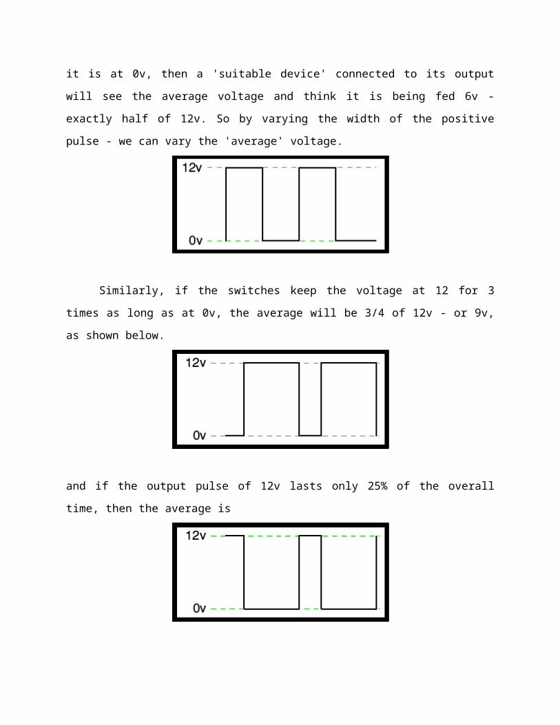
Step response of the DPFC: series converter voltage.
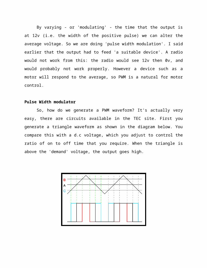
Step response of the DPFC: line current.
Step response of the DPFC: bus voltage and current at the Δ side of the transformer.

Step response of the DPFC: active and reactive power injected by the series converter at the fundamental frequency.
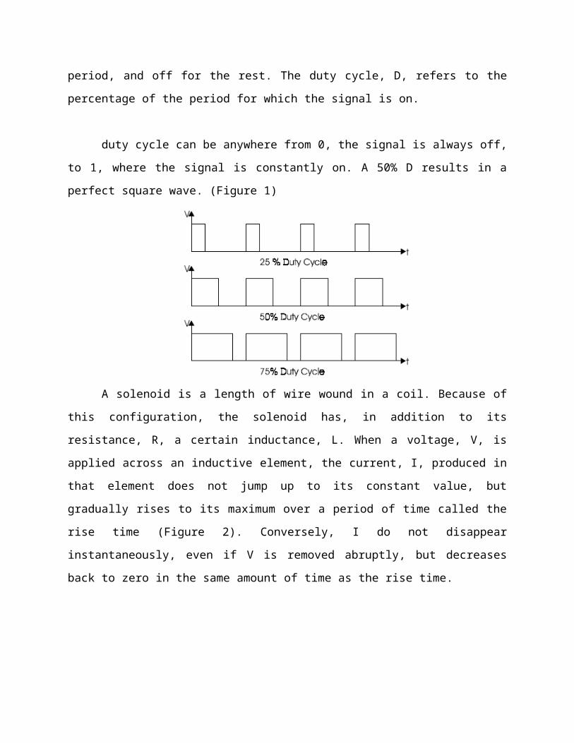
CONCLUSION
This paper has presented a new concept called DPFC. The DPFC emerges from the UPFC and
inherits the control capability of the UPFC, which is the simultaneous adjustment of the line
impedance, the transmission angle, and the bus-voltage magnitude. The common dc link between
the shunt and series converters, which is used for exchanging active power in the UPFC, is
eliminated. This power is now transmitted through the transmission line at the third-harmonic
frequency. The series converter of the DPFC employs the D-FACTS concept, which uses
multiple small single-phase converters instead of one large-size converter. The reliability of the
DPFC is greatly increased because of the redundancy of the series converters. The total cost of
the DPFC is also much lower than the UPFC, because no high-voltage isolation is required at the
series-converter part and the rating of the components of is low. The DPFC concept has been
verified by an experimental setup. It is proved that the shunt and series converters in the DPFC
can exchange active power at the third-harmonic frequency, and the series converters are able to
inject controllable active and reactive power at the fundamental frequency.
REFERENCES
[1] Y.-H. Song and A. Johns, Flexible ac Transmission Systems (FACTS) (IEE Power and
Energy Series), vol. 30. London, U.K.: Institution of Electrical Engineers, 1999.
[2] N. G. Hingorani and L. Gyugyi, Understanding FACTS: Concepts and Technology of
Flexible AC Transmission Systems. New York: IEEE Press, 2000.
[3] L.Gyugyi, C.D. Schauder, S. L.Williams, T. R. Rietman,D. R. Torgerson, And A. Edris, “The
unified power flow controller: A new approach to power transmission control,” IEEE Trans.
Power Del., vol. 10, no. 2, pp. 1085– 1097, Apr. 1995.
[4] A.-A. Edris, “Proposed terms and definitions for flexible ac transmission system (facts),”
IEEE Trans. Power Del., vol. 12, no. 4, pp. 1848–1853, Oct. 1997.
[5] K. K. Sen, “Sssc-static synchronous series compensator: Theory, modeling, and application,”
IEEE Trans. Power Del., vol. 13, no. 1, pp. 241–246, Jan. 1998.
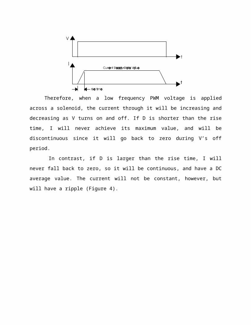
[6] M. D. Deepak, E. B. William, S. S. Robert, K. Bill, W. G. Randal, T. B. Dale, R. I. Michael,
and S. G. Ian, “A distributed static series compensator system for realizing active power flow
control on existing power lines,” IEEE Trans. Power Del., vol. 22, no. 1, pp. 642–649, Jan. 2007.
[7] D. Divan and H. Johal, “Distributed facts—A new concept for realizing grid power flow
control,” in Proc. IEEE 36th Power Electron. Spec. Conf. (PESC), 2005, pp. 8–14.
[8] Y. Zhihui, S.W. H. de Haan, and B. Ferreira, “Utilizing distributed power flow controller
(DPFC) for power oscillation damping,” in Proc. IEEE Power Energy Soc. Gen. Meet. (PES),
2009, pp. 1–5.
[9] Y. Zhihui, S. W. H. de Haan, and B. Ferreira, “Dpfc control during shunt converter failure,”
in Proc. IEEE Energy Convers. Congr. Expo. (ECCE) 2009, pp. 2727–2732.
[10] Y. Sozer and D. A. Torrey, “Modeling and control of utility interactive inverters,” IEEE
Trans. Power Electron., vol. 24, no. 11, pp. 2475–2483, Nov. 2009.


![“Control Strategy of AC/DC Hybrid Micro-Grid...inactive) where a PV solar farm is utilized as a Static Compensator (STATCOM) [20,22], a FACTS device for performing voltage control,](https://static.fdocuments.in/doc/165x107/5fb68b44eb6276128b4e738e/aoecontrol-strategy-of-acdc-hybrid-micro-grid-inactive-where-a-pv-solar-farm.jpg)