
A Controlling Method of Motor-Terminal Surge Voltage and ...
10
1 EVS25 Shenzhen, China, Nov 5-9, 2010 A Controlling Method of Motor-Terminal Surge Voltage and Induced-Electromagnetic Interference Noise for Electric Vehicles Nobuyoshi Mutoh 1 Takahiro Konuma 1 1 Graduate School of Tokyo Metropolitan University 6-6, Asahigaoka, Hino-shi, Tokyo, Japan [email protected] Abstract This paper describes a controlling method of motor-terminal surge voltage and induced-electromagnetic interference (EMI) noise which is effective in electric vehicles (EVs) with high density packaging structures. First, high frequency circuit parameters (HFCPs) to influence surges occurring at the motor terminals when a motor is connected to a pulse width modulation (PWM) inverter with short leads are clarified through transient circuit analyses and experiments. Then, a controlling method of the surge voltage and induced-EMI noise is proposed which uses a multi-layer power printed circuit. By applying the clarified HFCPs to an equivalent circuit expressing the multi-layer power printed circuit, damping resistance and bypass capacitance for suppressing surge voltage and the induced-EMI noise are determined. The effectiveness of the surge voltage and EMI noise controller using the values obtained through the analyses is verified through simulations and experiments. Keywords: EV (electric vehicle), EMI noise, motor-terminal surge, multi-layer power printed circuit, series resonance. 1 Introduction As one countermeasure against global warming, research and development of eco- vehicles, such as electric vehicles (EVs) and fuel cell vehicles, are being actively carried out. EVs are characterized by having the motor driving system as the propulsion power generating system to generate driving force. In order to be able to get high energy efficiency, it is necessary to design EVs with a compact configuration. To do so, a motor drive system with high density packaging is needed. However, in this high density structure, electromagnetic interference (EMI) noise generated due to high speed switching operations of pulse width modulation (PWM) inverters easily spreads over the passenger cabin of the vehicles through stray capacitance distributed over the drive system (Fig. 1) [1]. The electrical equipment in the vehicle may malfunction because of the diffused EMI noise. For this reason, in EVs with high density packaging, measures against EMI noise are indispensable. Since the motor drive systems of EVs generally have power converting devices such as PWM inverters to perform switching operations at high frequencies, a lot of leakage current flows to the body frame or the ground via the stray capacitance distributed EVS25 World Battery,Hybrid and Fuel Cell Electric Vehicle Symposium World Electric Vehicle Journal Vol. 4 - ISSN 2032-6653 - © 2010 WEVA Page000495
Transcript of A Controlling Method of Motor-Terminal Surge Voltage and ...
1
EVS25 Shenzhen, China, Nov 5-9, 2010
A Controlling Method of Motor-Terminal Surge Voltage and Induced-Electromagnetic Interference Noise for
Electric Vehicles
Nobuyoshi Mutoh1 Takahiro Konuma1 1 Graduate School of Tokyo Metropolitan University
6-6, Asahigaoka, Hino-shi, Tokyo, Japan [email protected]
Abstract This paper describes a controlling method of motor-terminal surge voltage and induced-electromagnetic
interference (EMI) noise which is effective in electric vehicles (EVs) with high density packaging
structures. First, high frequency circuit parameters (HFCPs) to influence surges occurring at the motor
terminals when a motor is connected to a pulse width modulation (PWM) inverter with short leads are
clarified through transient circuit analyses and experiments. Then, a controlling method of the surge
voltage and induced-EMI noise is proposed which uses a multi-layer power printed circuit. By applying the
clarified HFCPs to an equivalent circuit expressing the multi-layer power printed circuit, damping
resistance and bypass capacitance for suppressing surge voltage and the induced-EMI noise are determined.
The effectiveness of the surge voltage and EMI noise controller using the values obtained through the
analyses is verified through simulations and experiments.
Keywords: EV (electric vehicle), EMI noise, motor-terminal surge, multi-layer power printed circuit, series resonance.
1 Introduction As one countermeasure against global
warming, research and development of eco-vehicles, such as electric vehicles (EVs) and fuel cell vehicles, are being actively carried out. EVs are characterized by having the motor driving system as the propulsion power generating system to generate driving force. In order to be able to get high energy efficiency, it is necessary to design EVs with a compact configuration. To do so, a motor drive system with high density packaging is needed. However, in this high density structure, electromagnetic interference
(EMI) noise generated due to high speed switching operations of pulse width modulation (PWM) inverters easily spreads over the passenger cabin of the vehicles through stray capacitance distributed over the drive system (Fig. 1) [1]. The electrical equipment in the vehicle may malfunction because of the diffused EMI noise. For this reason, in EVs with high density packaging, measures against EMI noise are indispensable. Since the motor drive systems of EVs generally have power converting devices such as PWM inverters to perform switching operations at high frequencies, a lot of leakage current flows to the body frame or the ground via the stray capacitance distributed
EVS25 World Battery,Hybrid and Fuel Cell Electric Vehicle Symposium
World Electric Vehicle Journal Vol. 4 - ISSN 2032-6653 - © 2010 WEVA Page000495
2
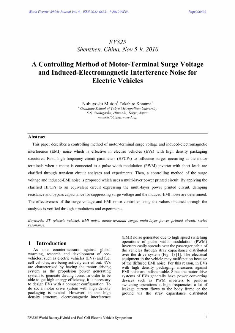
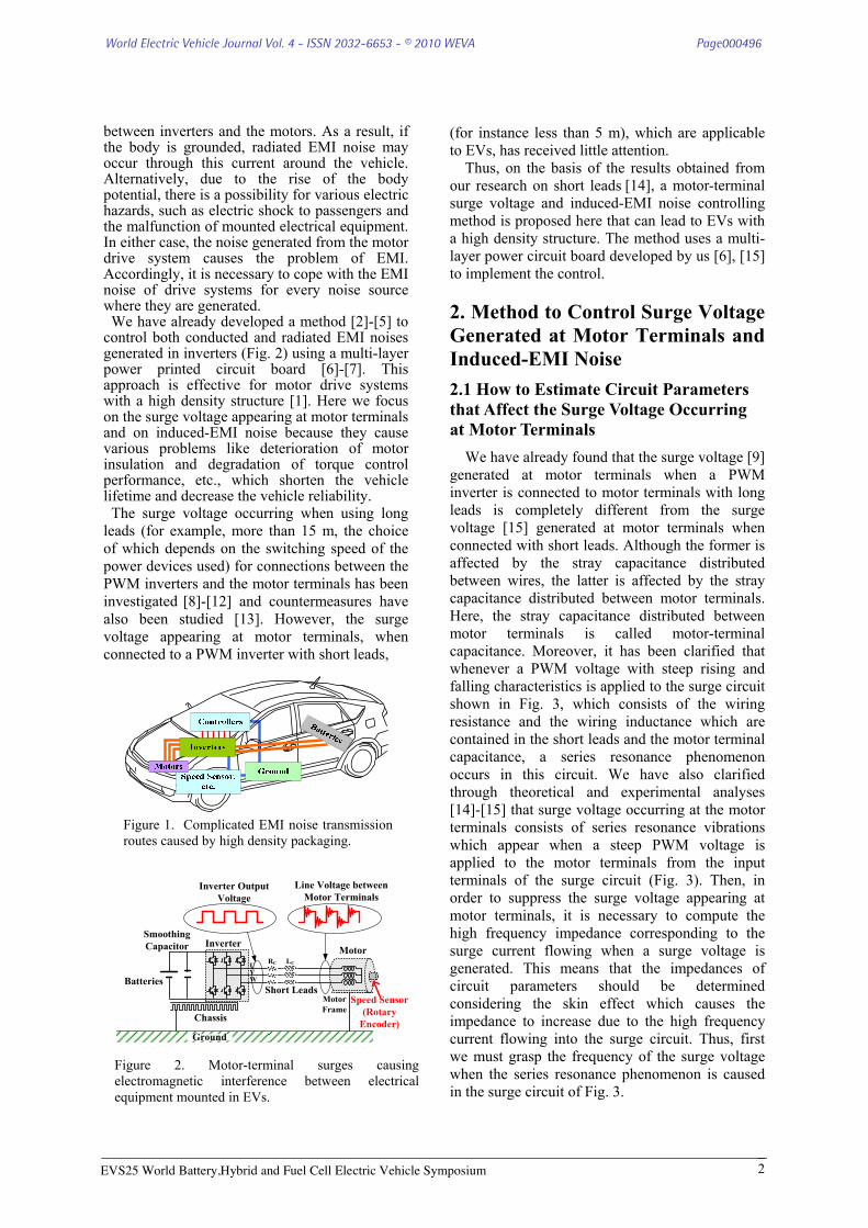
between inverters and the motors. As a result, if the body is grounded, radiated EMI noise may occur through this current around the vehicle. Alternatively, due to the rise of the body potential, there is a possibility for various electric hazards, such as electric shock to passengers and the malfunction of mounted electrical equipment. In either case, the noise generated from the motor drive system causes the problem of EMI. Accordingly, it is necessary to cope with the EMI noise of drive systems for every noise source where they are generated. We have already developed a method [2]-[5] to control both conducted and radiated EMI noises generated in inverters (Fig. 2) using a multi-layer power printed circuit board [6]-[7]. This approach is effective for motor drive systems with a high density structure [1]. Here we focus on the surge voltage appearing at motor terminals and on induced-EMI noise because they cause various problems like deterioration of motor insulation and degradation of torque control performance, etc., which shorten the vehicle lifetime and decrease the vehicle reliability. The surge voltage occurring when using long leads (for example, more than 15 m, the choice of which depends on the switching speed of the power devices used) for connections between the PWM inverters and the motor terminals has been investigated [8]-[12] and countermeasures have also been studied [13]. However, the surge voltage appearing at motor terminals, when connected to a PWM inverter with short leads,
(for instance less than 5 m), which are applicable to EVs, has received little attention.
Thus, on the basis of the results obtained from our research on short leads [14], a motor-terminal surge voltage and induced-EMI noise controlling method is proposed here that can lead to EVs with a high density structure. The method uses a multi-layer power circuit board developed by us [6], [15] to implement the control.
2. Method to Control Surge Voltage Generated at Motor Terminals and Induced-EMI Noise 2.1 How to Estimate Circuit Parameters that Affect the Surge Voltage Occurring at Motor Terminals
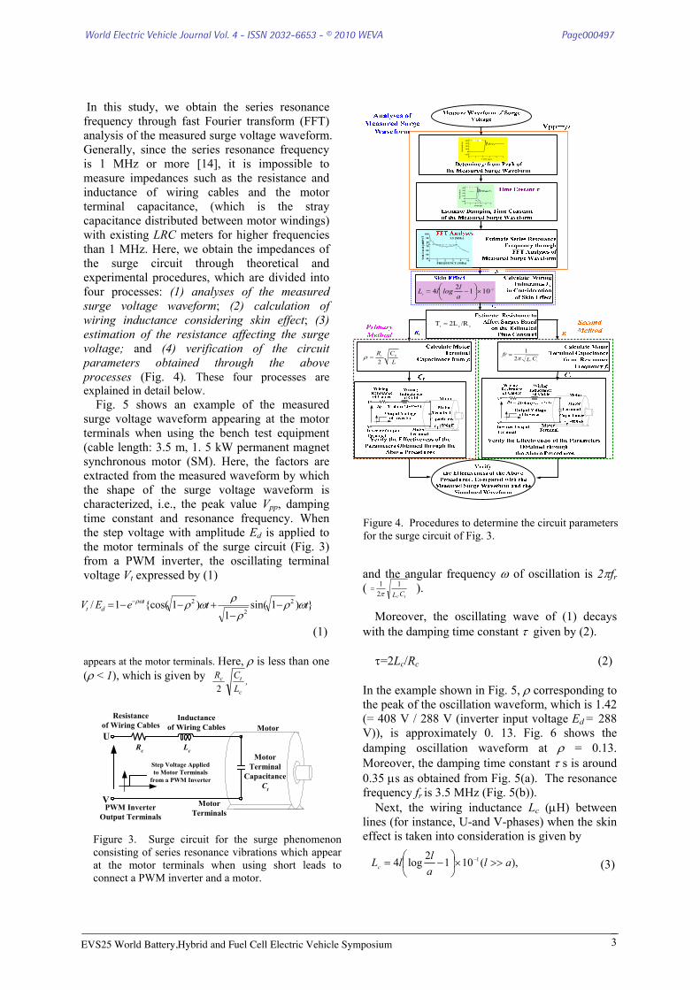
We have already found that the surge voltage [9] generated at motor terminals when a PWM inverter is connected to motor terminals with long leads is completely different from the surge voltage [15] generated at motor terminals when connected with short leads. Although the former is affected by the stray capacitance distributed between wires, the latter is affected by the stray capacitance distributed between motor terminals. Here, the stray capacitance distributed between motor terminals is called motor-terminal capacitance. Moreover, it has been clarified that whenever a PWM voltage with steep rising and falling characteristics is applied to the surge circuit shown in Fig. 3, which consists of the wiring resistance and the wiring inductance which are contained in the short leads and the motor terminal capacitance, a series resonance phenomenon occurs in this circuit. We have also clarified through theoretical and experimental analyses [14]-[15] that surge voltage occurring at the motor terminals consists of series resonance vibrations which appear when a steep PWM voltage is applied to the motor terminals from the input terminals of the surge circuit (Fig. 3). Then, in order to suppress the surge voltage appearing at motor terminals, it is necessary to compute the high frequency impedance corresponding to the surge current flowing when a surge voltage is generated. This means that the impedances of circuit parameters should be determined considering the skin effect which causes the impedance to increase due to the high frequency current flowing into the surge circuit. Thus, first we must grasp the frequency of the surge voltage when the series resonance phenomenon is caused in the surge circuit of Fig. 3.
Figure 1. Complicated EMI noise transmission routes caused by high density packaging.
Motor
Chassis
UVW
Inverter
Line Voltage between Motor Terminals
RC LC
Ground
Short LeadsBatteries
Motor Frame
Inverter Output Voltage
Smoothing Capacitor
Speed Sensor(Rotary
Encoder)
Figure 2. Motor-terminal surges causing electromagnetic interference between electrical equipment mounted in EVs.
EVS25 World Battery,Hybrid and Fuel Cell Electric Vehicle Symposium
World Electric Vehicle Journal Vol. 4 - ISSN 2032-6653 - © 2010 WEVA Page000496
3
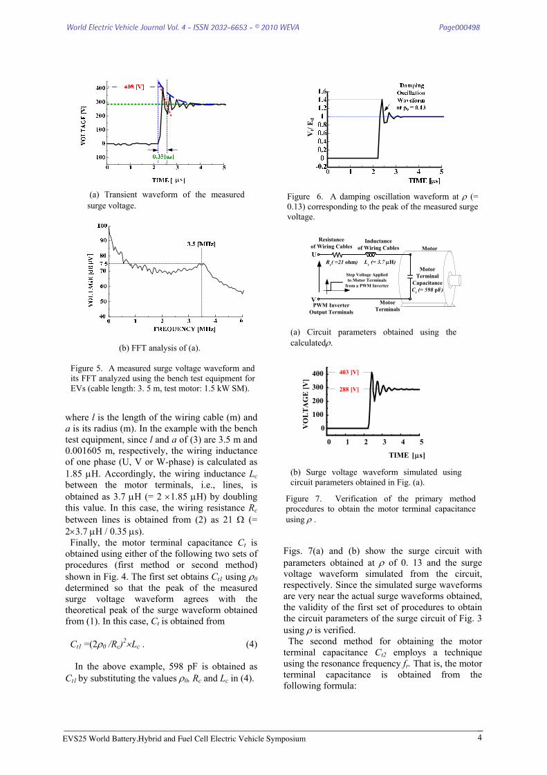
In this study, we obtain the series resonance frequency through fast Fourier transform (FFT) analysis of the measured surge voltage waveform. Generally, since the series resonance frequency is 1 MHz or more [14], it is impossible to measure impedances such as the resistance and inductance of wiring cables and the motor terminal capacitance, (which is the stray capacitance distributed between motor windings) with existing LRC meters for higher frequencies than 1 MHz. Here, we obtain the impedances of the surge circuit through theoretical and experimental procedures, which are divided into four processes: (1) analyses of the measured surge voltage waveform; (2) calculation of wiring inductance considering skin effect; (3) estimation of the resistance affecting the surge voltage; and (4) verification of the circuit parameters obtained through the above processes (Fig. 4). These four processes are explained in detail below.
Fig. 5 shows an example of the measured surge voltage waveform appearing at the motor terminals when using the bench test equipment (cable length: 3.5 m, 1. 5 kW permanent magnet synchronous motor (SM). Here, the factors are extracted from the measured waveform by which the shape of the surge voltage waveform is characterized, i.e., the peak value Vpp, damping time constant and resonance frequency. When the step voltage with amplitude Ed is applied to the motor terminals of the surge circuit (Fig. 3) from a PWM inverter, the oscillating terminal voltage Vt expressed by (1) (1) appears at the motor terminals. Here, U is less than one (U < 1), which is given by
and the angular frequency Z of oscillation is 2Sfr ( ).
Moreover, the oscillating wave of (1) decays with the damping time constant W given by (2). W=2Lc/Rc (2) In the example shown in Fig. 5, U corresponding to the peak of the oscillation waveform, which is 1.42 (= 408 V / 288 V (inverter input voltage Ed = 288 V)), is approximately 0. 13. Fig. 6 shows the damping oscillation waveform at U = 0.13. Moreover, the damping time constant W s is around 0.35 Ps as obtained from Fig. 5(a). The resonance frequency fr is 3.5 MHz (Fig. 5(b)).
Next, the wiring inductance Lc (PH) between lines (for instance, U-and V-phases) when the skin effect is taken into consideration is given by (3)
Motor
MotorTerminal
CapacitanceCt
PWM InverterOutput Terminals
MotorTerminals
Resistanceof Wiring Cables
Inductanceof Wiring Cables
Step Voltage Appliedto Motor Terminals
from a PWM Inverter
Rc Lc
U
V
Figure 3. Surge circuit for the surge phenomenon consisting of series resonance vibrations which appear at the motor terminals when using short leads to connect a PWM inverter and a motor.
-1 0 0
0
1 0 0
2 0 0
3 0 0
4 0 0
VO
LTA
GE
[V]
T IM E [P s ]543210
V p p
408 [V]
0.35 [Ps]-100
0
100
200
300
400
VO
LT
AG
E [V
]
TIME [Ps]543210
3.5 [MHz]
0 1 2 3 4 1640
50
60
70
80
90
100
VO
LT
AG
E [d
BP
V]
FREQUENCY [MHz]
7 5
/R2L T ccr
110124 �u¸¹·
¨©§ �
alloglLc
LCR bt
2 U
tc CLfr
S21
Figure 4. Procedures to determine the circuit parameters for the surge circuit of Fig. 3.
})1sin(1
)1{cos(1/ 2
2
2 tteEV tdt ZU
UUZUUZ ��
��� �tcCL
121S
),(1012log4 1 alallLc !!u¸
¹·
¨©§ � �
,LCR
c
tc
2
EVS25 World Battery,Hybrid and Fuel Cell Electric Vehicle Symposium
World Electric Vehicle Journal Vol. 4 - ISSN 2032-6653 - © 2010 WEVA Page000497
4
where l is the length of the wiring cable (m) and a is its radius (m). In the example with the bench test equipment, since l and a of (3) are 3.5 m and 0.001605 m, respectively, the wiring inductance of one phase (U, V or W-phase) is calculated as 1.85 PH. Accordingly, the wiring inductance Lc between the motor terminals, i.e., lines, is obtained as 3.7 PH (= 2 u1.85 PH) by doubling this value. In this case, the wiring resistance Rc between lines is obtained from (2) as 21 : (= 2u3.7 PH / 0.35 Ps). Finally, the motor terminal capacitance Ct is obtained using either of the following two sets of procedures (first method or second method) shown in Fig. 4. The first set obtains Ct1 using U0 determined so that the peak of the measured surge voltage waveform agrees with the theoretical peak of the surge waveform obtained from (1). In this case, Ct is obtained from
Ct1 =(2U0 /Rc)2uLc . (4)
In the above example, 598 pF is obtained as Ct1 by substituting the values U0, Rc and Lc in (4).
Figs. 7(a) and (b) show the surge circuit with parameters obtained at U of 0. 13 and the surge voltage waveform simulated from the circuit, respectively. Since the simulated surge waveforms are very near the actual surge waveforms obtained, the validity of the first set of procedures to obtain the circuit parameters of the surge circuit of Fig. 3 using U is verified.
The second method for obtaining the motor terminal capacitance Ct2 employs a technique using the resonance frequency fr. That is, the motor terminal capacitance is obtained from the following formula:
(a) Transient waveform of the measured surge voltage.
(b) FFT analysis of (a).
Figure 5. A measured surge voltage waveform and its FFT analyzed using the bench test equipment for EVs (cable length: 3. 5 m, test motor: 1.5 kW SM).
Vt/
Ed
Figure 6. A damping oscillation waveform at U (= 0.13) corresponding to the peak of the measured surge voltage.
Motor
MotorTerminal
CapacitanceCt (= 598 pF)
PWM InverterOutput Terminals
MotorTerminals
Resistanceof Wiring Cables
Inductanceof Wiring Cables
Step Voltage Appliedto Motor Terminals
from a PWM Inverter
Rc( =21 ohm) Lc (= 3.7 PH)U
V
(a) Circuit parameters obtained using the calculatedU.
0 1 2 3 4 5
0
100
200
300
400
VO
LTA
GE
[V]
TIME [Ps]
403 [V]
288 [V]
(b) Surge voltage waveform simulated using circuit parameters obtained in Fig. (a).
Figure 7. Verification of the primary method procedures to obtain the motor terminal capacitance using U .
EVS25 World Battery,Hybrid and Fuel Cell Electric Vehicle Symposium
World Electric Vehicle Journal Vol. 4 - ISSN 2032-6653 - © 2010 WEVA Page000498
5
Ct2 = (2Sfr)2 u Lc. (5) In the example with the bench test equipment, if the motor terminal capacitance Ct is computed from (5), 559 pF is obtained using the resonance frequency fr 3.5 MHz, which is the FFT analyzed result of Fig. 5(b). Fig. 8(b) shows the surge voltage waveform obtained using the surge circuit of Fig. 8(a). When compared with the actual surge voltage waveform shown in Fig. 5(a), we prove that the second method procedures are also effective. Therefore, it is possible to obtain the parameters of the surge circuits from either of the sets of procedures. However, the circuit parameters should be determined by comparing results obtained from the two sets of procedures with an actual measured surge voltage waveform. This is because errors occur when estimating these circuit parameters since both methods acquire them differently.
2.2 Surge Voltage and Induced-EMI Noise Controlling Method
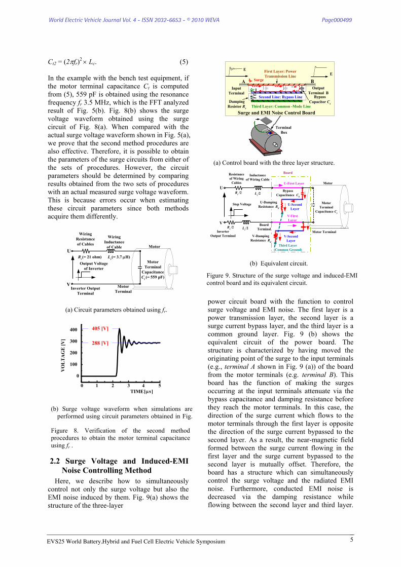
Here, we describe how to simultaneously control not only the surge voltage but also the EMI noise induced by them. Fig. 9(a) shows the structure of the three-layer
power circuit board with the function to control surge voltage and EMI noise. The first layer is a power transmission layer, the second layer is a surge current bypass layer, and the third layer is a common ground layer. Fig. 9 (b) shows the equivalent circuit of the power board. The structure is characterized by having moved the originating point of the surge to the input terminals (e.g., terminal A shown in Fig. 9 (a)) of the board from the motor terminals (e.g. terminal B). This board has the function of making the surges occurring at the input terminals attenuate via the bypass capacitance and damping resistance before they reach the motor terminals. In this case, the direction of the surge current which flows to the motor terminals through the first layer is opposite the direction of the surge current bypassed to the second layer. As a result, the near-magnetic field formed between the surge current flowing in the first layer and the surge current bypassed to the second layer is mutually offset. Therefore, the board has a structure which can simultaneously control the surge voltage and the radiated EMI noise. Furthermore, conducted EMI noise is decreased via the damping resistance while flowing between the second layer and third layer.
Motor
MotorTerminal
CapacitanceCt (= 559 pF)
Inverter OutputTerminal
MotorTerminal
WiringResistanceof Cables
WiringInductance
of Cable
Output Voltageof Inverter
Rc(= 21 ohm) Lc(= 3.7 PH)U
V
(a) Circuit parameters obtained using fr.
(b) Surge voltage waveform when simulations are performed using circuit parameters obtained in Fig. ( )
0 1 2 3 4 5
0
100
200
300
400
VO
LTA
GE
[V]
TIME
[Ps]
405 [V]
288 [V]
Figure 8. Verification of the second method procedures to obtain the motor terminal capacitance using fr .
Surge and EMI Noise Control Board
Terminal Box
InputTerminal
First Layer: PowerTransmission Line
OutputTerminal B
Second Line: Bypass Line
I
Third Layer: Common -Mode Line
A BE
Surge
BypassCapacitor CsDamping
Resistor Rs
E
(a) Control board with the three layer structure.
Motor
MotorTerminal
Capacitance Ct
InverterOutput Terminal
Motor Terminal
Resistanceof Wiring
Cables
Inductanceof Wiring Cable
Step Voltage
Rc /2 Lc/2Bypass
Capacitance Cb
U
V BoardTerminal
Board
U-First Layer
V-SecondLayer
Third Layer(Common Ground)
V-FirstLayer
U-SecondLayer
U-DampingResistance Rd
Rc /2
V-DampingResistance Rd
Lc/2
(b) Equivalent circuit.
Figure 9. Structure of the surge voltage and induced-EMI control board and its equivalent circuit.
EVS25 World Battery,Hybrid and Fuel Cell Electric Vehicle Symposium
World Electric Vehicle Journal Vol. 4 - ISSN 2032-6653 - © 2010 WEVA Page000499
6
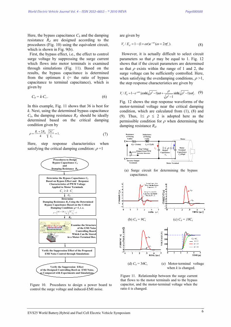
Here, the bypass capacitance Cb and the damping resistance Rd are designed according to the procedures (Fig. 10) using the equivalent circuit, which is shown in Fig. 9(b). First, the bypass effect, i.e., the effect to control surge voltage by suppressing the surge current which flows into motor terminals is examined through simulations (Fig. 11). Based on the results, the bypass capacitance is determined from the optimum k (= the ratio of bypass capacitance to terminal capacitance), which is given by
Cb = k�Ct . (6) In this example, Fig. 11 shows that 36 is best for k. Next, using the determined bypass capacitance Cb, the damping resistance Rd should be ideally determined based on the critical damping condition given by (7) Here, step response characteristics when satisfying the critical damping condition: U =1
]
are given by (8)
However, it is actually difficult to select circuit
parameters so that U may be equal to 1. Fig. 12 shows that if the circuit parameters are determined so that U exists within the range of 1 and 2, the surge voltage can be sufficiently controlled. Here, when satisfying the overdamping conditions, U >1, the step response characteristics are given by
(9) Fig. 12 shows the step response waveforms of the motor-terminal voltage near the critical damping condition, which are calculated from (1), (8) and (9). Thus, 1d U d 2 is adopted here as the permissible condition for U when determining the damping resistance Rd.
Determine the Bypass Capacitance Cb Based on Bypass Effect and Response
Characteristics of PWM Voltage Applied to Motor Terminals
Determine Damping Resistance Rd Using the Determined
Bypass Capacitance Based on the Critical Damping Condition:�U =1, i. e.
Examine the Structure of the EMI Noise
Controlling Board Which Can Be Stored
in a Motor-Terminal Box.
Verify the Suppression Effect of the Proposed EMI Noise Control through Simulations
Procedures to Design Bypass Capacitance Cb
and Damping Resistance Rd
Verify the Suppression Effect of the Designed Controlling Bord on EMI Noise, as Compared with Experiments and Simulations
tb CkC �tCb
Rd
Surge and E M I N oise C ontrol B oard
T erm inal B ox
InputT erm inal
First L ayer: Pow erT ransm issio n L ine
O utputT erm inal B
Seco nd L ine: B ypass L ine
I
T hird L ay er: C om m on -M ode L ine
A BE
Surge
B ypassC apacitor C sD am ping
R esistor R s
E
124
)2( ¸¹·¨
©§ �
c
bdc
LCRRU
Figure 10. Procedures to design a power board to control the surge voltage and induced-EMI noise.
Motor
MotorTerminal
CapacitanceCt:559pF
Inverter OutputTerminals Motor Terminal
Resistanceof Wiring
Cables
Inductanceof Wiring
Cable
Step VoltageOutput from PWMInverter Inverter
Rc(= 21ohm) Lc(=3.7PH)
BypassCapacitance
Cb
U
V
Isb Ist
(a) Surge circuit for determining the bypass capacitance.
(b) Cb = 9Ct (c) Cb = 18Ct
0 1 2 3 4 5
0
100
200
300
400
VO
LTA
GE
[V]
TIME [Ps]
Cb= kCtk = 9
k = 36
k = 18
(e) Motor-terminal voltage when k is changed.
(d) Cb = 36Ct
Figure 11. Relationship between the surge current that flows to the motor terminals and to the bypass capacitor, and the motor-terminal voltage when the ratio k is changed.
.1242
�
c
bdc
LCRRU
`2 2
2/ 1 {cosh( 1) sinh( 1) .
1t
t dV E e t tUZ UU Z U ZU
� � � � ��
21 dd U
).2()1(1/ rt
dt fetEV SZZ Z �� �
EVS25 World Battery,Hybrid and Fuel Cell Electric Vehicle Symposium
World Electric Vehicle Journal Vol. 4 - ISSN 2032-6653 - © 2010 WEVA Page000500
7
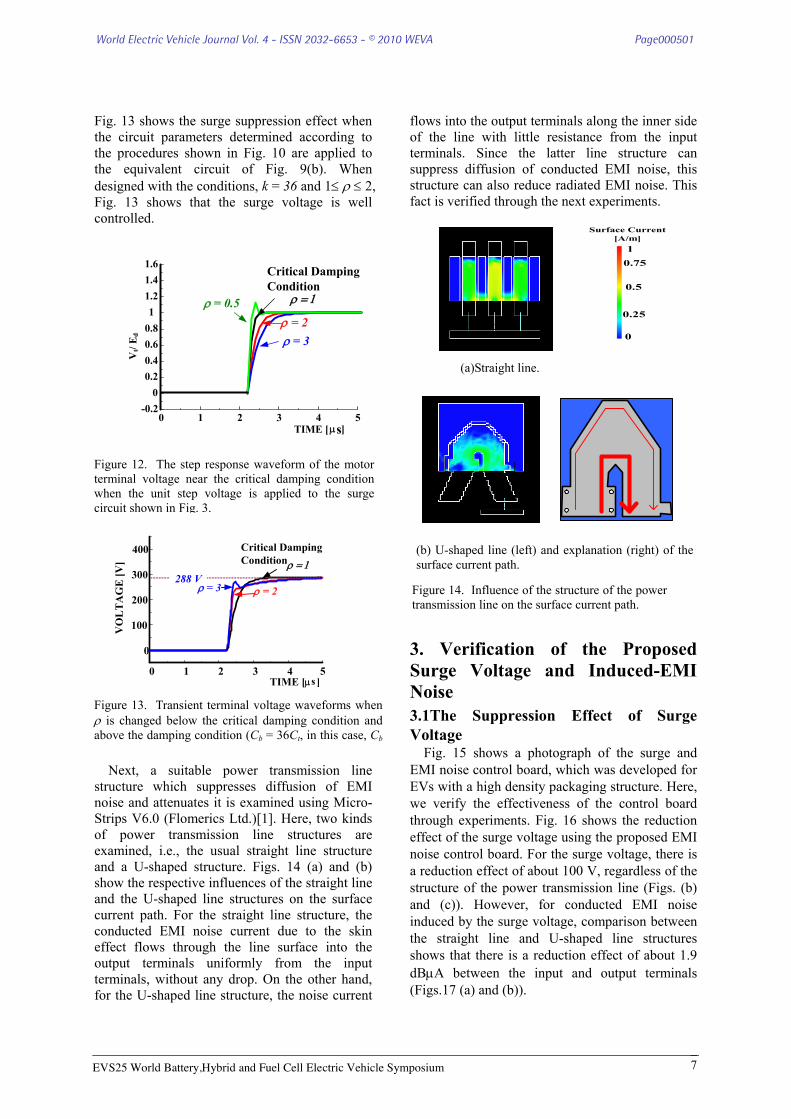
Fig. 13 shows the surge suppression effect when the circuit parameters determined according to the procedures shown in Fig. 10 are applied to the equivalent circuit of Fig. 9(b). When designed with the conditions, k = 36 and 1d U d 2, Fig. 13 shows that the surge voltage is well controlled.
Next, a suitable power transmission line structure which suppresses diffusion of EMI noise and attenuates it is examined using Micro-Strips V6.0 (Flomerics Ltd.)[1]. Here, two kinds of power transmission line structures are examined, i.e., the usual straight line structure and a U-shaped structure. Figs. 14 (a) and (b) show the respective influences of the straight line and the U-shaped line structures on the surface current path. For the straight line structure, the conducted EMI noise current due to the skin effect flows through the line surface into the output terminals uniformly from the input terminals, without any drop. On the other hand, for the U-shaped line structure, the noise current
flows into the output terminals along the inner side of the line with little resistance from the input terminals. Since the latter line structure can suppress diffusion of conducted EMI noise, this structure can also reduce radiated EMI noise. This fact is verified through the next experiments.
3. Verification of the Proposed Surge Voltage and Induced-EMI Noise 3.1The Suppression Effect of Surge Voltage Fig. 15 shows a photograph of the surge and EMI noise control board, which was developed for EVs with a high density packaging structure. Here, we verify the effectiveness of the control board through experiments. Fig. 16 shows the reduction effect of the surge voltage using the proposed EMI noise control board. For the surge voltage, there is a reduction effect of about 100 V, regardless of the structure of the power transmission line (Figs. (b) and (c)). However, for conducted EMI noise induced by the surge voltage, comparison between the straight line and U-shaped line structures shows that there is a reduction effect of about 1.9 dBPA between the input and output terminals (Figs.17 (a) and (b)).
0 1 2 3 4 5-0.2
00.20.40.60.81
1.21.41.6
TIME [Ps
Critical Damping Condition
U = 2U�= 3
U� ��
Vt/
E d
U�= 0.5
]
Figure 12. The step response waveform of the motor terminal voltage near the critical damping condition when the unit step voltage is applied to the surge circuit shown in Fig. 3.
0 1 2 3 4 5
0
100
200
300
400
VO
LTA
GE
[ V]
TIME [Ps ]
288 V
Critical Damping Condition
U = 2U�= 3
U� ��
Figure 13. Transient terminal voltage waveforms when U is changed below the critical damping condition and above the damping condition (Cb = 36Ct, in this case, Cb
(a)Straight line.
0
0.25
0.5
0.751
Surface Current[A/m]
(b) U-shaped line (left) and explanation (right) of the surface current path.
Figure 14. Influence of the structure of the power transmission line on the surface current path.
EVS25 World Battery,Hybrid and Fuel Cell Electric Vehicle Symposium
World Electric Vehicle Journal Vol. 4 - ISSN 2032-6653 - © 2010 WEVA Page000501

8
3.2 The Suppression Effect of EMI Noise Induced by Surge Voltage
Moreover, checking the component of the 3.5-MHz radiated noise produced with surge voltage shows us there reduction effect of 5 dBPA/m between the straight and U-shaped line structures (Fig. 18). The EMI noise control board has an effect not only for surge voltage control but for control of the radiated EMI noise produced by its surge voltage. However, even if the surge voltage is almost controlled, PWM voltage waveforms having steeply changing characteristics are repeatedly applied to the motor terminals (for example case (ii) of Fig. 19(a)). As a result, Fig.19(b) shows that a common mode current flows into the ground through the stray capacitance distributed between the motor
winding coil and frame (Fig. 19(b-1))[1], [3] and the current causes radiated EMI noise near 1.6
Figure 15. Photo of the surge voltage and EMI noise control board mounted in the motor-terminal box.
0 1 2 3 4 5-100
0100200300400
VO
LTA
GE
[V]
TIME [Ps]
408 [V]
(a) Without control.
0 1 2 3 4 5 6-100
0100200300400
VO
LTA
GE
[V]
TIME [Ps]
308 [V]
(b) With control (straight line).
(c) With control (U- shaped line).
0 1 2 3 4 5-100
0100200300400
VO
LTA
GE
[V]
TIME [P s]
296 [V]
Figure 16. Reduction effect of the surge voltage and EMI noise control board on surges appearing at the motor terminals (Rd = 30 :, Cb = 0.02 PF, which satisfy the design condition ofU).
(a) For straight line structure.
30 [mm]
9.1 [dBPA]
Output Terminalsof Control Boad
���>mm@
5.1 [dBPA] Reduction Effect:4.0 [dBPA]
Input Terminalsof Control Boad
(b) For U-shaped line structure.
Figure 17. Reduction effect of the surge voltage and EMI noise controlling board on conducted EMI noises.
0 1 2 3 4 540
50
60
70
80
90
M
AG
NE
TIC
FIE
LD
[dBPA
/m]
3 . 5 [ M H z ]
20 [dBPA/m]
With Controlling Method
Without Controlling Method
FREQUENCY[MHz]
0 1 2 3 4 540
50
60
70
80
90
FREQUENCY[MHz]
MA
GN
ET
IC F
IEL
D[d
BPA
/m] 3 . 5 M H z
25 [dBPA/m]
Without Controlling Method
With Controlling Method
1 . 6 M H z
(a) Effect for straight line structure.
Figure 18. The suppression effect of the surge and EMI noise controlling board on the radiated EMI noise (magnetic field) at about a 3 cm height.
(b) Effect for U-shaped line structure.
EVS25 World Battery,Hybrid and Fuel Cell Electric Vehicle Symposium
World Electric Vehicle Journal Vol. 4 - ISSN 2032-6653 - © 2010 WEVA Page000502

9
MHz. The common mode current can be almost completely suppressed using our previously proposed technique [3] (Fig.19(c-1)) and generating of the EMI radiated noise seen at 1.6 MHz is also prevented (Fig.19(c-2)). Therefore, in order to reduce EMI noise produced in the motor drive systems for EVs effectively, it is necessary to also prevent common mode current simultaneously with suppression of the surge voltage generated in motor terminals.
4. Conclusion A method to simultaneously control surge
voltages occurring at motor terminals and EMI noise induced by them was described here. The method is especially effective in EVs with high density packaging structures. This method is realized using a multi-layer power circuit board with a three-layer structure. The first layer is a power transmission layer, the second layer is a surge current bypass layer, and the third layer is a common ground layer. In this power circuit board, the bypass capacitor is connected between the first and second layers and the damping resistance is connected between the second and third layers. The effect of the proposed control method was verified through simulations and experiments. The surge voltage and the induced-EMI noise controlling method is very effective for EVs with high density structures. It is important to control the common mode current which occurs by repeatedly applying the PWM voltage with rapidly changing characteristics to motors simultaneously with control of the surge voltage.
References [1] N Mutoh, M Nakanishi, M Kanesaki, J Nakashima,
“EMI noise control methods suitable for electric vehicle drive systems”, IEEE Trans. on EMC, vol. 47, no. 4, pp. 930-937 (2005).
[2] N. Mutoh, M. Ogata, K. Gulez, F. Harashima, “New methods to suppress EMI noises in motor drive systems”, IEEE Transaction on Industrial Electronics, vol. 49, no. 2, pp.474-485 (2002).
[3] N. Mutoh, M. Ogata, “New methods to control EMI noises generated in motor drive systems”, IEEE Transactions on Industry Applications, vol. 40, no. 1, pp. 143-152 (2004).
[4] N. Mutoh, J. Nakashima, M. Kanesaki, “A new method to control EMI noises generated in power converters”, Industrial Electronics Society, 2003. IECON '03, The 29th Annual Conference of the IEEE, Nov.2-6, vol. 3, pp. 2753-2758 (2003).
[5] N. Mutoh, M. Kanesaki, J. Nakashima, M. Ogata, “ A new method to control common mode currents focusing on common mode current paths produced in motor drive systems“, Industry Applications Conference, 2003 (IAS2003), Conference Record of the 38th IAS Annual Meeting, vol. 1, Oct.12-16, pp. 459-466 (2003).
[6] N. Mutoh, J. Nakashima, M. Kanesaki, “Multilayer power printed structures suitable for controlling EMI noises generated in power converters” IEEE Transactions on Industrial Electronics (IES), vol. 53, no. 6, pp. 1085-1094 (2003).
[7] N. Mutoh, M. Ogata, J. Nakashima, M. Kanesaki, “A new method to control EMI noises appearing in power converters by a multi-layer power printed circuit technique”, EPE 2003, CD-ROM, September 2-4 (2003).
0 1 2 3 4
-100
0
100
200
300
400
VO
LT
AG
E V
TIME Ps
(ii) With only the countermeasures against the surge voltage
(i) Without the countermeasures against the surge voltage and
common mode current
0 1 2 3 4 5
P
FREQUENCY MHz
3.5 MHz
Mag
netic
Fie
ld d
B
(ii)
(i)
40
50
60
70
80
90
A/m 1.6 MHz
0 1 2 3 4 5
Mag
netic
Fie
ld [d
BP
]
FREQUENCY [MHz]
V/m
40
50
60
70
80
901.6MHz (i)
(ii)
(iii)
0 1 2 3 4-1
0
1
2
CU
RR
EN
T A
TIME Ps
(i)(ii)
(iii) With countermeasures against the surge
voltage and common mode
current
(a)Surge suppression effect using the countermeasures shown in Fig.18 (b)
(b) EMI noise still caused by common mode current even if the surge voltage is suppressed.
0 1 2 3 4-1
0
1
2
CU
RR
EN
T A
TIME Ps
(i)(ii)
(c) EMI noise suppression effects when both the surge voltage and common mode current are suppressed
Figure 19. The suppression effect of EMI noise suppression effects when the surge voltage and the common mode current are controlled at the same time.
(b-1) (b-2)
(c-1) (c-2)
EVS25 World Battery,Hybrid and Fuel Cell Electric Vehicle Symposium
World Electric Vehicle Journal Vol. 4 - ISSN 2032-6653 - © 2010 WEVA Page000503
10
[8] M. Bentley, P.J. Link, “Evaluation of motor power cables for PWM ac drives”, IEEE Trans. on Industry Applications, vol. 33, no. 2, pp. 342-358 (1997).
[9] N. Aoki, K. Satoh, A. Kabae, “Damping circuit to suppress terminal overvoltage and ringing in PWM Inverter-fed ac motor drive systems with Long Motor Leads”, IEEE Trans. on Industry Applications, vol. 35, no. 5, pp. 1014-102 (1999).
[10] A. von Jouanne, D. A. Rendusara, P. N. Enjeti, J. W. Gray, “Filtering techniques to minimize the effect of long motor leads on PWM inverter-fed ac motor drive systems”, IEEE Trans. on Industry Applications, vol. 32, no. 4, pp. 919-926 (1996).
[11] S. Moriyasu, Y. Okuyama, “Surge propagation of PWM-inverter and surge voltage on the motor”, Trans. IEE J Japan, vol. 119-D, no.4, pp.508-514 (1999).
[12] A. F. Moreira, P. M. Santos, T. A. Lipo, G. Venkataramanan, “Filter networks for long cable drives and their influence on motor voltage distribution and common-mode currents”, IEEE Transactions on Industrial Electronics, vol. 52, no. 2, pp. 515- 522 (2005).
[13] A. von Jouanne, P.N Enjeti, “Design considerations for an inverter output filter to mitigate the effects of long motor leads in ASD applications”, IEEE Trans. on Industry Applications, vol. 33, no. 5, pp. 1138-1145 (1997).
[14] N. Mutoh, M. Kanesaki, J. Nakashima, “A method to control EMI noises generated by micro-surges appearing at terminals of electric machines connected to power converters via electric power wirings “, Applied Power Electronics Conference and Exposition, CD-ROM Proceedings of Nineteenth Annual IEEE.
[15] N. Mutoh, M. Kanesaki, “A Suitable Method for Eco-vehicles to Control Surge Voltage Occurring at Motor Terminals Connected to PWM Inverters and to Control Induced EMI Noise “, IEEE Trans. on Vehicular Technology, vol. 57, no.4, pp.2089-2098 (2008).
Authors Dr. Nobuyoshi Mutoh,
Professor, Graduate School of Tokyo Metropolitan University, [email protected]. Major fields are advanced echo-machine control systems such as EVs. PV, wind power and fuel cells. IEEE senior member, Professional Engineer (Electronics and Electronics)
Mr. Takahiro Konuma
Honda Motors Co. Ltd. He received the MS degree in the Department of Systems Design of the Graduate School, Tokyo Metropolitan University. His area of research is EMI noise control for EVs and advanced EV control systems.
EVS25 World Battery,Hybrid and Fuel Cell Electric Vehicle Symposium
World Electric Vehicle Journal Vol. 4 - ISSN 2032-6653 - © 2010 WEVA Page000504