A CMOS Analog Front-End Circuit for Micro-Fluxgate · PDF fileA Thesis Presented in Partial...
59
1 A CMOS Analog Front-End Circuit for Micro-Fluxgate Sensors by Karthik Pappu A Thesis Presented in Partial Fulfillment of the Requirements for the Degree Master of Science Approved August 2013 by the Graduate Supervisory Committee: Bertan Bakkaloglu, Chair Jennifer Blain Christen Hongbin Yu ARIZONA STATE UNIVERSITY December 2013
-
Upload
truongkien -
Category
Documents
-
view
222 -
download
3
Transcript of A CMOS Analog Front-End Circuit for Micro-Fluxgate · PDF fileA Thesis Presented in Partial...
1
A CMOS Analog Front-End Circuit for Micro-Fluxgate Sensors
by
Karthik Pappu
A Thesis Presented in Partial Fulfillment of the Requirements for the Degree
Master of Science
Approved August 2013 by the Graduate Supervisory Committee:
Bertan Bakkaloglu, Chair Jennifer Blain Christen
Hongbin Yu
ARIZONA STATE UNIVERSITY
December 2013

i
ABSTRACT
Fluxgate sensors are magnetic field sensors that can measure DC and low
frequency AC magnetic fields. They can measure much lower magnetic fields than other
magnetic sensors like Hall effect sensors, magnetoresistive sensors etc. They also have
high linearity, high sensitivity and low noise. The major application of fluxgate sensors is
in magnetometers for the measurement of earth’s magnetic field. Magnetometers are used
in navigation systems and electronic compasses. Fluxgate sensors can also be used to
measure high DC currents. Integrated micro-fluxgate sensors have been developed in
recent years. These sensors have much lower power consumption and area compared to
their PCB counterparts. The output voltage of micro-fluxgate sensors is very low which
makes the analog front end more complex and results in an increase in power
consumption of the system.
In this thesis a new analog front-end circuit for micro-fluxgate sensors is
developed. This analog front-end circuit uses charge pump based excitation circuit and
phase delay based read-out chain. With these two features the power consumption of
analog front-end is reduced. The output is digital and it is immune to amplitude noise at
the output of the sensor. Digital output is produced without using an ADC. A SPICE
model of micro-fluxgate sensor is used to verify the operation of the analog front-end and
the simulation results show very good linearity.

ii
ACKNOWLEDGMENTS
I am very grateful to my advisor and committee chair Dr. Bertan Bakkaloglu for
his guidance, encouragement and patience. He is the source of my inspiration. I would
like to give special appreciation to Dr. Jennifer Blain Christen and Dr. Hongbin Yu for
being a part of my thesis defense committee.
I am thankful to my project mates Mr. Koushik Malladi, Mr. Abhiram
Mummareddy, Mr. Vivek Parasuram, Mr. Amit Kumar, Mr. Navankur Beohar and Mr.
Chao Fu for their support, knowledge sharing and interactive discussions.
I would like to thank Mr. James Laux for his support regarding software. I would
also like to thank all my professors for their knowledge sharing during my course work.
I am thankful to my parents, sister and my family for their support and
encouragement. I would like to thank all my friends for their support and friendship.

iii
TABLE OF CONTENTS
Page
LIST OF TABLES ................................................................................................................ ....v
LIST OF FIGURES .............................................................................................................. ...vi
CHAPTER
1 INTRODUCTION ............................................................................................. ...1
1.1 Background ....................................................................................... 1
1.2 Research Goals ................................................................................. 2
1.3 Operating Principle of Fluxgate Sensor ........................................... 3
1.4 Second Harmonic Principle .............................................................. 3
1.5 Ring-type Fluxgate Sensor ............................................................... 5
1.6 Phase Delay Principle ....................................................................... 6
1.7 Miniature Fluxgate Magnetic Sensors ............................................. 9
1.8 Spice Model of Micro-fluxgate Sensor .......................................... 11
2 STATE-OF-THE-ART ANALOG FRONT-END CIRCUITS ....................... 15
2.1 A CMOS Front-End Circuit for Integrated Fluxgate Sensors ....... 15
2.2 A CMOS 2D Micro-Fluxgate Earth Magnetic Field Sensor ......... 17
2.3 Low-Voltage Fluxgate Sensor Interface Circuit ............................ 20
3 ANALOG FRONT-END ARCHITECTURE .................................................. 22
3.1 Excitation Circuit ............................................................................ 25
3.1.1 Charge Pump ......................................................................... 25
3.1.2 Triangular Current Generator ............................................... 30
3.1.3 Current Sink .......................................................................... 32
iv
CHAPTER Page
3.1.4 H-Bridge ................................................................................ 34
3.2 Read-out Chain ............................................................................... 36
3.2.1 Double Differential Preamplifier .......................................... 36
3.2.2 Comparator ............................................................................ 38
3.2.3 Time to Digital Converter ..................................................... 40
3.3 Layout ............................................................................................. 42
4 RESULTS .......................................................................................................... 43
5 CONCLUSION .................................................................................................. 48
REFERENCES ...................................................................................................................... 49
v
LIST OF TABLES
Table Page
1.1 Parameters of Ring-type Micro-Fluxgate Sensor .................................................. 14
2.1 Key Specifications .................................................................................................. 17
2.2 Key Specifications .................................................................................................. 19
4.1 Key Specifications of Developed Analog Front-End .......................................... 47

vi
LIST OF FIGURES
Figure Page
1.1 Basic Fluxgate Sensor Principle .............................................................................. 3
1.2 Ring-type Fluxgate Sensor ...................................................................................... 6
1.3 Output of a Single Core Fluxgate Sensor ............................................................... 7
1.4 Output of a Ring-type Fluxgate Sensor .................................................................. 8
1.5 SPICE Model of Magnetic Core ........................................................................... 11
1.6 B-H Curve .............................................................................................................. 12
1.7 SPICE Model of Fluxgate Sensor ......................................................................... 13
2.1 A CMOS Front-End Circuit for Integrated Fluxgate Sensors.............................. 16
2.2 Excitation Circuit ................................................................................................... 16
2.3 CMOS 2D Micro-Fluxgate Earth Magnetic Field Sensor ................................... 18
2.4 3.3V Excitation Circuit ......................................................................................... 20
2.5 5V Excitation Circuit and Read-Out Chain .......................................................... 21
3.1 Excitation Circuit ................................................................................................... 23
3.2 Read-Out Chain ..................................................................................................... 24
3.3 Charge Pump ......................................................................................................... 26
3.4 Output of Charge Pump ........................................................................................ 27
3.5 Reset Pulse Generation Circuit ............................................................................. 28
3.6 Triangular Current Generator ................................................................................ 30
3.7 Current Sink ........................................................................................................... 33
3.8 H-Bridge Circuit .................................................................................................... 34
vii
Figure Page
3.9 Excitation Current Waveforms ............................................................................. 35
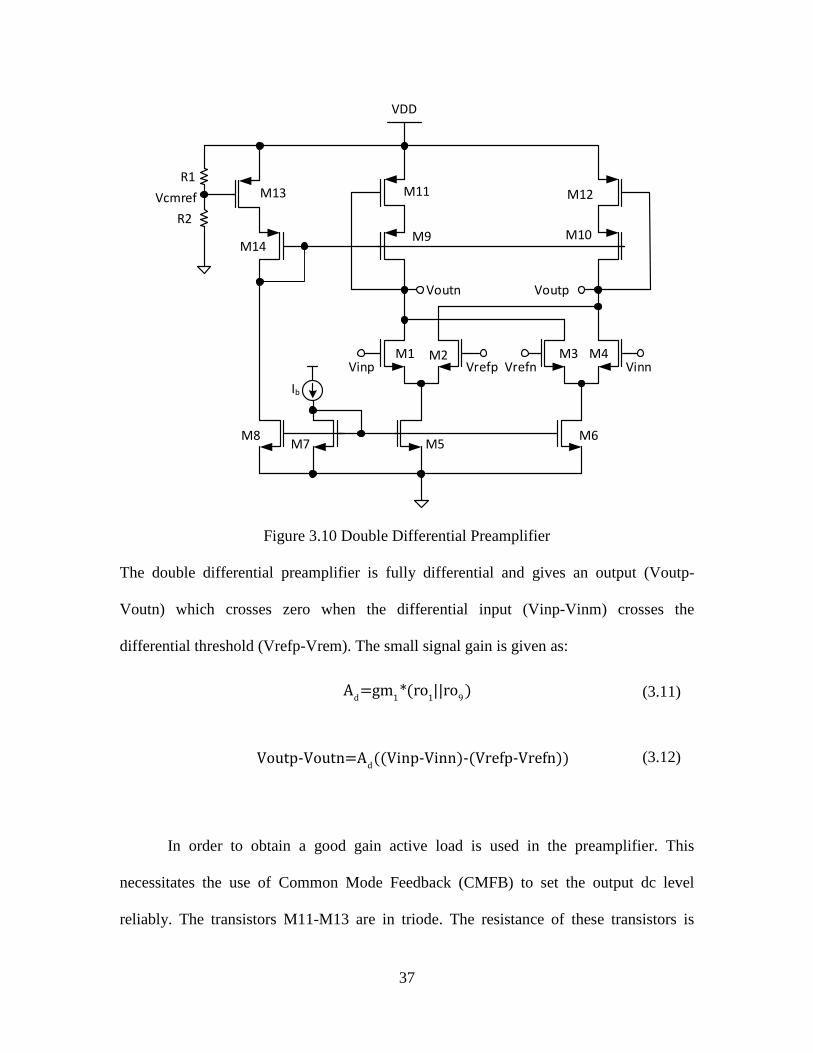
3.10 Double Differential Preamplifier ........................................................................ 37
3.11 Current-mode Comparator .................................................................................. 39
3.12 Time to Digital Converter ................................................................................... 41
3.13 Time to Digital Converter Waveforms ............................................................... 41
3.14 Layout of Analog Front-End Circuit .................................................................. 42
4.1 Charge Pump Output Voltage ............................................................................... 43
4.2 Excitation Current Waveform ............................................................................... 44
4.3 Output of Micro-Fluxgate Sensor ......................................................................... 45
4.4 Output of Sensor and Comparator vs External Magnetic Field ........................... 45
4.5 Difference between Sensor and Comparator Output vs External Magnetic field ........................................................................................................ 46
4.6 %Linearity Error vs External Magnetic Field ...................................................... 46
4.7 Digital Output vs External Magnetic Field ........................................................... 47

1
Chapter 1
INTRODUCTION
1.1 Background
Fluxgate sensors are magnetic sensors that can measure DC and low frequency
AC magnetic fields. They are capable of measuring magnetic fields order of nT to one
mT with resolution as low as 10pT [1]. They are also sensitive to the direction of
magnetic field. These sensors have very high linearity, sensitivity, low noise and
ruggedness. They can measure much lower magnetic fields than other magnetic field
sensors like Hall sensors, magnetoresistive sensors, search coil magnetometers etc. with
good linearity. SQUIDs (super conducting quantum interference devices) are the only
magnetic sensors which have higher sensitivity than fluxgate sensors and they are very
expensive.
The following are a few important applications of fluxgate sensors [2] [3] [4] [7].
• Earth magnetic field measurement in magnetometers for navigation systems and
electronic compasses
• Detection of minerals and ores
• Space Magnetometers
• Measurement of DC and low frequency AC currents
• Mechanical measurements such as linear and angular position, displacement and
velocity etc.

2
1.2 Research Goals
Conventional PCB fluxgate sensors consume a large amount of area and power
which limits the application of these sensors. Low power, low area micro-fluxgate
sensors are developed over the past few years increasing the possibility of realizing
magnetic micro systems.
One of the major challenges of integrated micro-fluxgate sensors is the realization of
magnetic core. Micro-fluxgate sensors are mostly realized either in a CMOS process
where the magnetic core is realized using post processing [5] - [7] or using MEMS
processes [8] [9] [12].
Although micro-fluxgate sensors offer great savings in area and power they
produce much lower outputs compared to the traditional PCB fluxgate sensors. This
makes the analog front-end circuit for micro-fluxgate sensors to be more complex and it
also consumes more power. Portable devices and wireless sensor networks require low
power sensor systems. Hence along with a reduction of power of the sensor it is
important to realize low power analog front end circuits.
The goal of this thesis is to address to develop a new low power analog front-end
circuit for micro-fluxgate sensors which has the following properties
• Low power
• ADC free digital output
• Produces an output that varies linearly with external magnetic field
• Can be integrated with other CMOS circuits

3
1.3 Operating Principle of Fluxgate Sensor
The fluxgate sensor consists of an excitation coil, a sensing coil and a magnetic core. The
current through the excitation coil should be high enough to saturate the core in one
direction or the other twice per each cycle. When the core is not saturated it offers a low
reluctance path to the external magnetic field and when the core is saturated it offers a
high reluctance path to the external magnetic field, there by gating the external flux.
Hence the sensor is called a fluxgate. This change in flux induces a voltage in the sensing
coil [10].
µ(t) B(t)
Iexc(t)
Vind
Bext
Figure 1.1 Basic Fluxgate Sensor Principle
1.4 Second Harmonic Principle
The second harmonic of the output voltage across the sensing coil of a fluxgate
sensor is proportional to the external magnetic field [11]. If a sinusoidal current of
frequency ω/2π is used to excite the fluxgate sensor it creates a magnetic field Href given
by equation (1.1). The external magnetic field Hext will be added to this.
ref refmaxH =H sinωt (1.1)

4
If N is the demagnetization factor and µ is the relative permeability, the magnetic field
within the core is given by:
This magnetic field is normalized to H0* which is given as:
The normalized magnetic field strength within the core is given by:
The magnetization curve can be approximated by a normalized third order polynomial as:
where b is the normalized flux density
The output voltage across the sensing coil is given as:
where N is the number of turns of the sensing coil and A is the area of cross section of the
magnetic core.
ext refmax
int
r
H +H sinωtH =
1+N(μ -1) (1.2)
* sat r
0
r 0
B [1+N(μ -1)]2H =
π μ μ (1.3)
int
int ext refmax*
0
Hh = =h +h sinωt
H (1.4)
3
1 3b(h)=a h-a h (1.6)
3
1 ext 1 refmax 3 ext refmaxb(h)=a h +a h sinωt-a (h +h sinωt) (1.7)
out
d dBV N NA
dt dt
φ= − = − (1.8)

5
The normalized output voltage is given as:
The second-harmonic component of the voltage across the sensing coils is given as:
Given that all other factors are constant the amplitude of second harmonic is proportional
to the external magnetic field strength.
1.5 Ring-type Fluxgate Sensor
It can be seen from equation (1.10) that the output of the sensor also contains DC
and first harmonic contents and hence it would require a bandpass filter to extract the
second harmonic. A ring-type fluxgate sensor [12] would produce an output that does not
contain the DC and first harmonic components. The output now contains only the even
harmonics. Therefore the second harmonic can be obtained by low-pass filtering. It
would also reduce the current required to saturate the magnetic core because the flux is
now flowing in a closed path.
out
out 0
V dB dBv B
NA dt dt= − = = (1.9)
= ω − − ω +
ω ω + ω ω
2 2 3
out 0 1 ref max 3 ext ref max 3 ref max
2 3
0 3 ext ref max 0 3 ref max
v B (a h 3a h h 0.75a h )cos t
3B a h h sin2 t 0.75B a h cos3 t (1.10)
2
out2h 0 3 ext ref maxV 3B NA a h h sin2 t= − ω ω (1.11)
6
Excitation Coil
Sensing Coil
Magnetic Core
Iexc
Vdiff
Bext
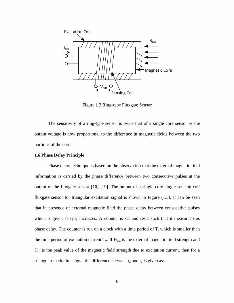
Figure 1.2 Ring-type Fluxgate Sensor
The sensitivity of a ring-type sensor is twice that of a single core sensor as the
output voltage is now proportional to the difference in magnetic fields between the two
portions of the core.
1.6 Phase Delay Principle
Phase delay technique is based on the observation that the external magnetic field
information is carried by the phase difference between two consecutive pulses at the
output of the fluxgate sensor [10] [19]. The output of a single core single sensing coil
fluxgate sensor for triangular excitation signal is shown in Figure (1.3). It can be seen
that in presence of external magnetic field the phase delay between consecutive pulses
which is given as t2-t1 increases. A counter is set and reset such that it measures this
phase delay. The counter is run on a clock with a time period of Ts which is smaller than
the time period of excitation current T0. If Hext is the external magnetic field strength and
Hm is the peak value of the magnetic field strength due to excitation current, then for a
triangular excitation signal the difference between t2 and t1 is given as:

7
The counter output Ns is given by:
Vcoil
t1t2
t
t
t1 t2
Vcoil
Without external magnetic field
With external magnetic field
Figure 1.3 Output of a Single Core Fluxgate Sensor
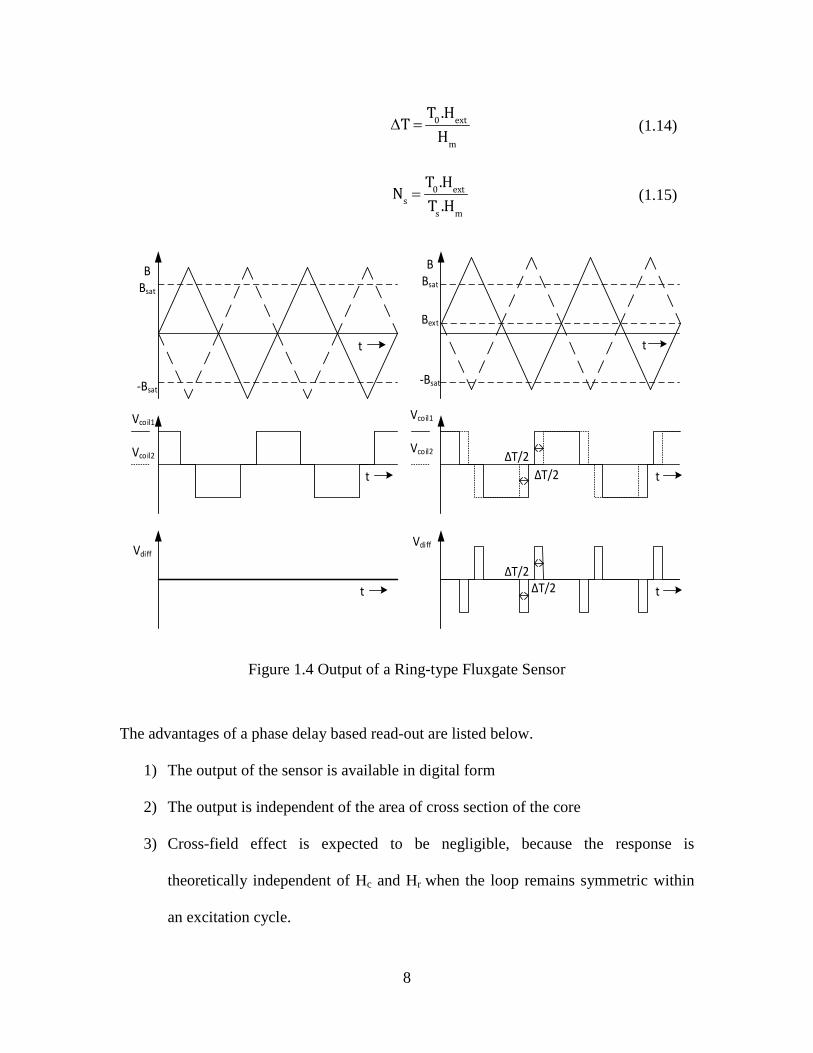
The output waveforms for a ring-type sensor with triangular excitation signal are
shown in Figure (1.4). It can be seen that the phase delay t2-t1 transforms into the pulse
width of the output voltage across the sensing coils. The sensitivity of the sensor is also
doubled because the difference in magnetic field strengths associated with the respective
portions of the core is now twice the external magnetic field. The output of a ring-type
sensor is given as:
0 ext
2 1
m
T .Ht t T
2H− = ∆ = (1.12)
0 ext
s
s m
T .HN
2T .H= (1.13)
8
B
Bsat
Vcoil1
Vcoil2
Vdiff
Vdiff
-Bsat
B
Bsat
-Bsat
Bext
Vcoil1
Vcoil2
t
t
t
t
∆T/2
∆T/2
∆T/2
∆T/2
t
t
Figure 1.4 Output of a Ring-type Fluxgate Sensor
The advantages of a phase delay based read-out are listed below.
1) The output of the sensor is available in digital form
2) The output is independent of the area of cross section of the core
3) Cross-field effect is expected to be negligible, because the response is
theoretically independent of Hc and Hr when the loop remains symmetric within
an excitation cycle.
0 ext
m
T .HT
H∆ = (1.14)
0 ext
s
s m
T .HN
T .H= (1.15)

9
4) The receiving coil properties do not influence the sensor’s output considerably as
long as the output voltage has amplitude greater than the noise floor. Hence coils
of inferior characteristics such as integrated coils can be used for fabricating the
sensor.
1.7 Miniature Fluxgate Magnetic Sensors
Miniaturization of fluxgate sensors enables the generation of micro-fluxgate
magnetic sensors that are cost effective, low power and have low area. Applications such
as current sensing, navigation systems and portable devices demand smaller fluxgate
sensors. Micro-fluxgate sensors can be integrated with the analog front end circuitry and
also other CMOS circuits and ASICs. The traditional fluxgate sensors have wound
excitation and sensing coils whose cost can be reduced using micro fabrication
techniques. The sensitive parts like the magnetic core are generally realized by post-
processing. The low power micro-fluxgate sensors integrated with other CMOS circuits
can be a part of smart sensor systems. Several state of the art micro-fluxgate sensors
fabricated using different processes are described in [5]-[9].
A ring-type micro-machined fluxgate sensor fabricated in UV-LIGA process has been
reported in [12]. Instead of saturating the entire core only a part of the core where the
sensing coil is placed is saturated by reducing the area of the core in these portions.
Hence the peak value of excitation current required to saturate the core reduced to 50mA
from 250mA. The peak to peak value of output voltage is around 30mV. A sensitivity of
389V/T has been obtained.
A comparison between a double axis PCB fluxgate sensor and an IC version is
made in [5]. The coils for the micro-fluxgate sensor have been fabricated in 0.5µm

10
CMOS technology and the ferromagnetic core is deposited using post processing. The
micro-fluxgate sensor yielded a 75% saving in area with respect to a direct scaling of the
PCB version. The IC version also showed a tremendous decrease in power consumption.
It required only 5mA peak current to saturate the core compared to 600mA of the PCB
fluxgate sensor. This shows that a great reduction in power and area can be obtained
using micro-fluxgate sensors.
While the micro-fluxgate sensors work at lower power and area they have
decreased sensitivity and more noise [5] [10]. The voltage across a coil wrapped around a
magnetic core excited by a sinusoidal current is given as:
where Nsense is the number of turns in the sensing coil, S is the cross section area of the
core, µ is the absolute magnetic permeability, Nexc is the number of turns in the excitation
coil, I0 is the amplitude of excitation current, fexc is the excitation frequency and lm is the
length of the magnetic path. Because of the area reduction the amplitude of the sensed
signal and hence the sensitivity of the sensor decrease with miniaturization. Due to this
reason the micro-fluxgate sensors are usually operated at much higher frequencies than
PCB sensors to get a voltage signal of amplitude good enough to be processed by the read
out circuitry. For example the PCB sensor in [5] works with an excitation frequency of
10KHz and produces an output with 15mV amplitude where as the IC version of it works
at an excitation frequency of 100KHz and produces an output with 1mV amplitude.
Micro-fluxgate sensors also have higher noise than that of PCB sensors.
exc 0 exc
ind sense
m
* N * I .sin(2 f t)d dV - - N *S * ( )
dt dt l
µ πΦ= = (1.16)
11
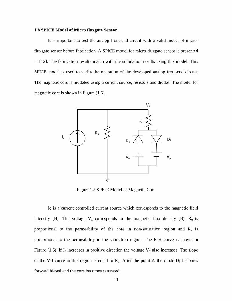
1.8 SPICE Model of Micro fluxgate Sensor
It is important to test the analog front-end circuit with a valid model of micro-
fluxgate sensor before fabrication. A SPICE model for micro-fluxgate sensor is presented
in [12]. The fabrication results match with the simulation results using this model. This
SPICE model is used to verify the operation of the developed analog front-end circuit.
The magnetic core is modeled using a current source, resistors and diodes. The model for
magnetic core is shown in Figure (1.5).
Ru
Rs
D2D1
Vn Vp
Ie
VX
Figure 1.5 SPICE Model of Magnetic Core
Ie is a current controlled current source which corresponds to the magnetic field
intensity (H). The voltage Vx corresponds to the magnetic flux density (B). Ru is
proportional to the permeability of the core in non-saturation region and Rs is
proportional to the permeability in the saturation region. The B-H curve is shown in
Figure (1.6). If Ie increases in positive direction the voltage Vx also increases. The slope
of the V-I curve in this region is equal to Ru. After the point A the diode D1 becomes
forward biased and the core becomes saturated.
12
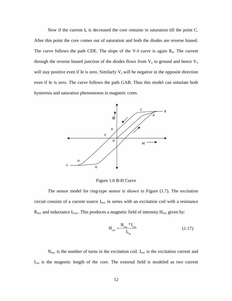
Now if the current Ie is decreased the core remains in saturation till the point C.
After this point the core comes out of saturation and both the diodes are reverse biased.
The curve follows the path CDE. The slope of the V-I curve is again Ru. The current
through the reverse biased junction of the diodes flows from Vx to ground and hence Vx
will stay positive even if Ie is zero. Similarly Vx will be negative in the opposite direction
even if Ie is zero. The curve follows the path GAB. Thus this model can simulate both
hysteresis and saturation phenomenon in magnetic cores.
O
D
E
B
A
C
FG
H
H
B
Figure 1.6 B-H Curve
The sensor model for ring-type sensor is shown in Figure (1.7). The excitation
circuit consists of a current source Iexc in series with an excitation coil with a resistance
Rexc and inductance Lexc. This produces a magnetic field of intensity Hexc given by:
Nexc is the number of turns in the excitation coil. Iexc is the excitation current and
Lm is the magnetic length of the core. The external field is modeled as two current
exc exc
exc
m
N *IH
L= (1.17)

13
sources Hext. So the magnetic field strength in one arm is Hexc+Hext and the magnetic field
in the other arm is Hexc-Hext.
Ru
Rs
D2D1
Vn Vp
Ru
Rs
D2 D1
Vn Vp
Hext
Hext
Hexc
Iexc
Rexc
Lexc
Isense11H
+
-
Isense21H
+
-
Vsensep
Vsensen
Vcm
Vcm
Vx
VY
Figure 1.7 SPICE Model of Fluxgate Sensor
Isense1 and Isense2 are voltage controlled current sources with gain proportional to
Nsense*A c, where Nsense is the number of turns in the sensing coils and Ac is the area of
cross section of the core. Vcm sets the common mode dc voltage at the output of the
sensing coils. The currents Isense1,2 are passed through inductors to produce the final
output voltages.
sense1 sense c XI N * A * V= (1.18)
sense2 sense c YI N * A * V= (1.19)
x
sense1 sense sense c
dVdV N * N * A *
dt dt
φ= = (1.20)

14
This sensor model has been tested with the fabricated micro-fluxgate sensors in
[13]. The results show good matching between the simulated and measured outputs.
Hence this model is used in this thesis. The parameters of the sensor fabricated in [13] are
shown in Table 1.1 below.
Parameter Value
Number of turns in excitation coil (Nexc) 44
Number of turns in sensing coils (Nsense) 14
Resistance of Excitation coil (Rexc) 3Ω
Inductance of Excitation coil (Lexc) 1.01µH
Length of the magnetic path (Lm) 700µm
Area of cross section (Ac) 700µm*100µm
Excitation Frequency 50KHz
Peak value of excitation current 50mA
Table 1.1 Parameters of Ring-type Micro-Fluxgate Sensor
Y
sense2 sense sense c
dVdV N * N * A *
dt dt
φ= = (1.21)

15
Chapter 2
STATE-OF-THE-ART ANALOG FRONT-END CIRCUITS
Traditional fluxgate sensors are excited using sinusoidal or pulse excitation [14].
Sinusoidal excitation provides low noise signals where as pulsed excitation is easier to
implement. Triangular excitation gives lower noise than pulse excitation and is easier to
implement compared to sinusoidal excitation [15]. Hence triangular excitation is most
suited for integrated fluxgate sensors. In this section a review of the existing state of the
art analog front-end circuits for micro fluxgate sensors are presented.
2.1 A CMOS Front-End Circuit for Integrated Fluxgate Sensors
The analog front-end circuit presented in [15] contains an excitation circuit, a
timing unit and a read-out unit. A 400KHz clock is divided internally to get a 100KHz
clock and 200KHz clock. The 100KHz clock is used in the excitation circuit to generate a
triangular voltage signal at 100KHz. The 200KHz clock is used to demodulate the output
of the fluxgate sensor. It is essential that these two clocks have a 50% duty cycle to
ensure proper demodulation.
A schematic of the excitation circuit is shown in Figure (2.1). It consists of an
integrator followed by a transconductance amplifier. The resistor and capacitor are on
chip but the input to the integrator ±Vin is external. This makes it possible to use the
system for sensors with different saturation current requirement. For one half of the clock
period of 100KHz clock the input is connected to +Vin and for the other half it is
connected to -Vin. This produces a triangular voltage wave around zero at the output of
the integrator. This triangular voltage is fed to a transconductance amplifier which
produces a triangular current. This current is passed through a current mirror into a class
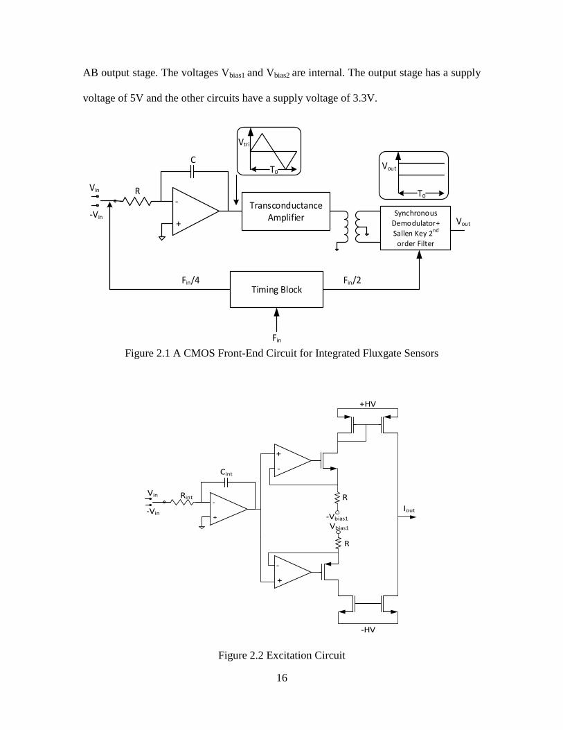
16
AB output stage. The voltages Vbias1 and Vbias2 are internal. The output stage has a supply
voltage of 5V and the other circuits have a supply voltage of 3.3V.
-
+
Transconductance
AmplifierSynchronous
Demodulator+
Sallen Key 2nd
order Filter
Vin
-Vin
R
C
Timing BlockFin/4 Fin/2
Fin
T0
Vtri
Vout
T0
Vout
Figure 2.1 A CMOS Front-End Circuit for Integrated Fluxgate Sensors
-
+
Vin
-Vin
Rint
Cint
+
-
-Vbias1
-
+
Vbias1
-HV
+HV
R
R
Iout
Figure 2.2 Excitation Circuit

17
Second harmonic principle is used to obtain the output signal. The read-out circuit
has a synchronous demodulation unit followed by a second order Sallen-Key low pass
filter to extract the second harmonic component of the output of the fluxgate sensor.
Some of the important specifications of this analog front-end circuit are listed in
Table (2.1). These results are obtained by testing the analog front end on a PCB fluxgate
sensor.
Process 0.35µm, 2 poly, 5 metal
Sensitivity 920V/T
Range ±60µT
Linearity 6 % F.S
Power Consumption
42 mW @ 5V
8mW @ 3.3V
Area without pads 1700*350µm2
Table 2.1 Key Specifications
The major disadvantage of this analog front end circuit is the use of symmetric
power supply for the generation of triangular current in both positive and negative
directions. Current CMOS technologies do not use symmetric power supplies and hence
it would be difficult to integrate this analog front-end circuit with other CMOS circuits
and ASICs. Also it does not provide the output in digital format.
2.2 A CMOS 2D Micro-fluxgate Earth Magnetic Field Sensor
A double axis micro-fluxgate sensor with its analog front-end circuit has been
presented in [7] and [16]. A 0.5µm CMOS process followed by post processing for the
magnetic core is used to fabricate the micro-fluxgate sensor. A new technique called dc-
magnetron sputtering is used which allows us to get a ferromagnetic core of good
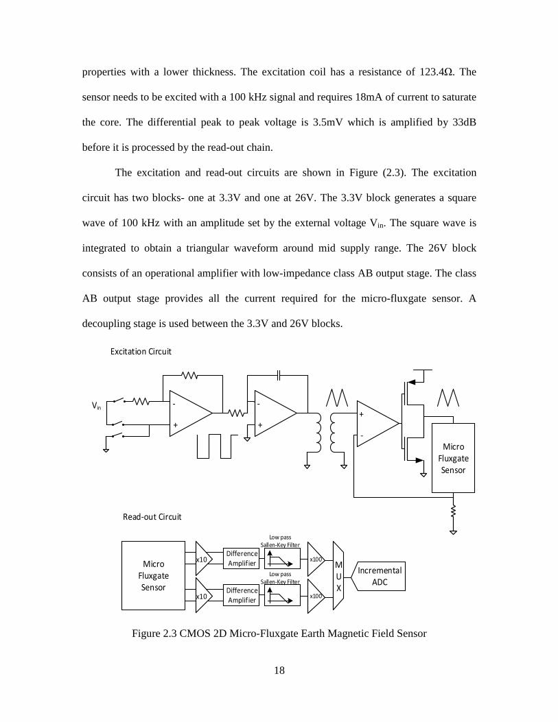
18
properties with a lower thickness. The excitation coil has a resistance of 123.4Ω. The
sensor needs to be excited with a 100 kHz signal and requires 18mA of current to saturate
the core. The differential peak to peak voltage is 3.5mV which is amplified by 33dB
before it is processed by the read-out chain.
The excitation and read-out circuits are shown in Figure (2.3). The excitation
circuit has two blocks- one at 3.3V and one at 26V. The 3.3V block generates a square
wave of 100 kHz with an amplitude set by the external voltage Vin. The square wave is
integrated to obtain a triangular waveform around mid supply range. The 26V block
consists of an operational amplifier with low-impedance class AB output stage. The class
AB output stage provides all the current required for the micro-fluxgate sensor. A
decoupling stage is used between the 3.3V and 26V blocks.
-
+
Vin-
++
-
Micro
Fluxgate
Sensor
Micro
Fluxgate
Sensor
x10Difference
Amplif ier
Low pass
Sallen-Key Filter
x100
x10Difference
Amplif ier
Low pass
Sallen-Key Filter
x100
M
U
X
Incremental
ADC
Excitation Circuit
Read-out Circuit
Figure 2.3 CMOS 2D Micro-Fluxgate Earth Magnetic Field Sensor

19
The differential output voltage is amplified by a factor of 10 and then passed
through a difference amplifier that amplifies the difference between the two outputs of
the sensing coils. A Sallen- Key filter is used to extract the second harmonic component
of the output voltage. The output of the Sallen- Key filter is amplified further before
being digitized by a 13bit incremental ADC. The salient features of this analog front end
circuit are provided in Table (2.2).
Sensor Technology 0.5µm CMOS
Ferromagnetic Core Vitrovac 6025 X deposited by DC-magnetron
sputtering
Interface circuit technology 0.35µm CMOS
Sensor Area 3.2mm2
Interface circuit area 1.7mm2
Supply Voltage 3.3V-26V
Power consumption of sensor 13.7mW
Power consumption of system 90mW
Magnetic field range ±60µT
Linearity Error 3% of full scale
Angle Error (Earth Magnetic
Field)
4º
Table 2.2 Key Specifications
This analog front-end also uses symmetric power supply to generate the triangular
current in both positive and negative directions and hence it would be difficult to
integrate it with other CMOS circuits. Also the power consumption for the analog front
end is around 76.3mW which is very high. In addition to these the use of a decoupling
stage increases the cost of the interface circuit.

20
2.3 Low-voltage Fluxgate Sensor Interface Circuit
A low-voltage fluxgate magnetic sensor interface circuit with digital output for
portable applications is presented in [17]. Two different excitation circuits have been
proposed. The excitation circuit that works at a relatively lower voltage of 3.3V is shown
in Figure (2.4). It consists of an H- bridge which changes the direction of current through
the excitation coil of the fluxgate sensor at the desired frequency thus eliminating the use
of split power supply. The 3.3V excitation circuit uses an external inductance of 380µH
to generate the triangular current waveform.
M6
M8
M7
M9
S1 S2Rs Ls
Vdd
VddT
Clk
Q
Q
S1
S2
VddT
Clk
Q
Q
Clk Lext
gnd
Figure 2.4 3.3V Excitation Circuit
The excitation circuit with 5V power supply has a triangular voltage generator, a
voltage to current converter and an H-bridge. A square wave is generated and then
integrated using an active integrator to obtain a triangular wave. This triangular voltage is
level shifted and converted into triangular current by using a voltage to current converter.
The current is mirrored using a cascode current mirror to get a 20mA peak current. The
peak value of the triangular current can be modified by changing the reference voltage
Vref which is set externally. The H-bridge is driven by signals S1 and S2 to switch
alternatively the current flowing into the excitation coil of the sensor. This would allow
the sensor to be excited with a 40mA peak to peak current without using symmetric
supply voltage.

21
-
+
Vref
-
+
S1
S2
S1
-
+Vdd/2
R1
R2
R3 R4
C1
R5
R6
R7
Vref2
+
-
Vdd/2gnd
M1
M2
M3 M4
M5
M6
M8
M7
M9
Vdd
S1 S2
Rrif
Rs Ls
Vdd
Clk
T
Clk
Q
Q
S1
S2
Excitation Circuit
x60 DEMUXSallen-Key
FilterPGA
Offset Control Offset Control
ADC
Read-Out Chain
Figure 2.5 5V Excitation Circuit and Read-Out Chain
The read-out chain presented is shown in Figure (2.5). It performs a synchronous
demodulation to obtain the extract the second harmonic component in the output of the
fluxgate sensor. The difference in the outputs of the sensing coils is amplified by 35dB
using an instrumentation amplifier. Each operational amplifier used in the
instrumentation amplifier consumes 168µW of power. The single ended output is
demodulated using a coherent orthogonal demodulator. The demodulation is done at a
frequency of 200KHz. A quadrature demodulator is used. The output of the demodulator
is passed through a Sallen- Key filter that produces a dc signal proportional to the second
harmonic component of the output voltage. The dc signal is amplified by a programmable
gain amplifier (PGA) before it is digitized by a 13 bit incremental ADC. The total power
consumed by the interface circuit and its area are not mentioned.
22
Chapter 3
ANALOG FRONT-END ARCHITECTURE
A review of the existing state-of-the-art analog front end circuits for micro-
fluxgate sensors presented in chapter 2 reveals that triangular excitation signal is
preferred as it gives good noise performance and is easier to generate. The proposed
analog front end circuit uses a charge pump based excitation circuit to generate the
triangular excitation current. The advantages of using phase delay technique to extract the
output signal in digitized form have been listed in section 1.6. The proposed analog front-
end circuit uses phase delay technique in the read-out chain.
The developed analog front-end architecture is shown in Figure (3.1) and Figure
(3.2). The excitation circuit consists of a charge pump which charges and discharges an
external capacitor CSET linearly to produce a triangular voltage waveform at its output.
This is done by alternatively turning on two constant current sources Ip and In. When the
clock goes low the capacitor CSET is charged through a constant current source Ip. When
the clock goes high the capacitor is discharged through the constant current source In.
This generates a triangular voltage at the output of the charge pump. The charge pump
works on a 100KHz clock. The triangular voltage is periodically reset to a fixed dc value
so as to provide a proper input common mode to the next stage.
The triangular voltage waveform generated by the charge pump is converted into
a triangular current by a voltage to current converter. The triangular voltage is applied
through a feedback loop across an external resistor RSET whose negative terminal is held
constant at a dc voltage Vsink. The external resistor sets the current in this branch. A
current sink with very low output impedance is used to set the voltage at the negative
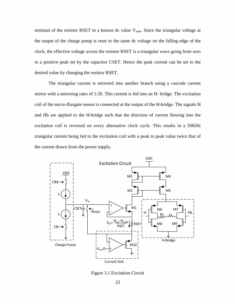
23
terminal of the resistor RSET to a known dc value Vsink. Since the triangular voltage at
the output of the charge pump is reset to the same dc voltage on the falling edge of the
clock, the effective voltage across the resistor RSET is a triangular wave going from zero
to a positive peak set by the capacitor CSET. Hence the peak current can be set to the
desired value by changing the resistor RSET.
The triangular current is mirrored into another branch using a cascode current
mirror with a mirroring ratio of 1:20. This current is fed into an H- bridge. The excitation
coil of the micro-fluxgate sensor is connected at the output of the H-bridge. The signals H
and Hb are applied to the H-bridge such that the direction of current flowing into the
excitation coil is reversed on every alternative clock cycle. This results in a 50KHz
triangular current being fed to the excitation coil with a peak to peak value twice that of
the current drawn from the power supply.
Clkb
Clk
Reset
+
-M1
M2
M3 M4
M5
M6
M8
M7
M9
H Hb
RSET
Rs Ls
CSET
-
+Vsink
Charge Pump
Current Sink
H-Bridge
Ip
In
Excitation CircuitVDD
VDD
M10
Itri=Vcp-Vsink
RSET
Vcp
Figure 3.1 Excitation Circuit
24
Micro
Fluxgate
Sensor Vrefp
Vrefn
+
-
+
-
Ad
+
-
Time to
Digital
Converter
Read-out chain
Double
Differential
Preamplifier
Comparator
Input
from
H-
bridge
Figure 3.2 Read-out chain
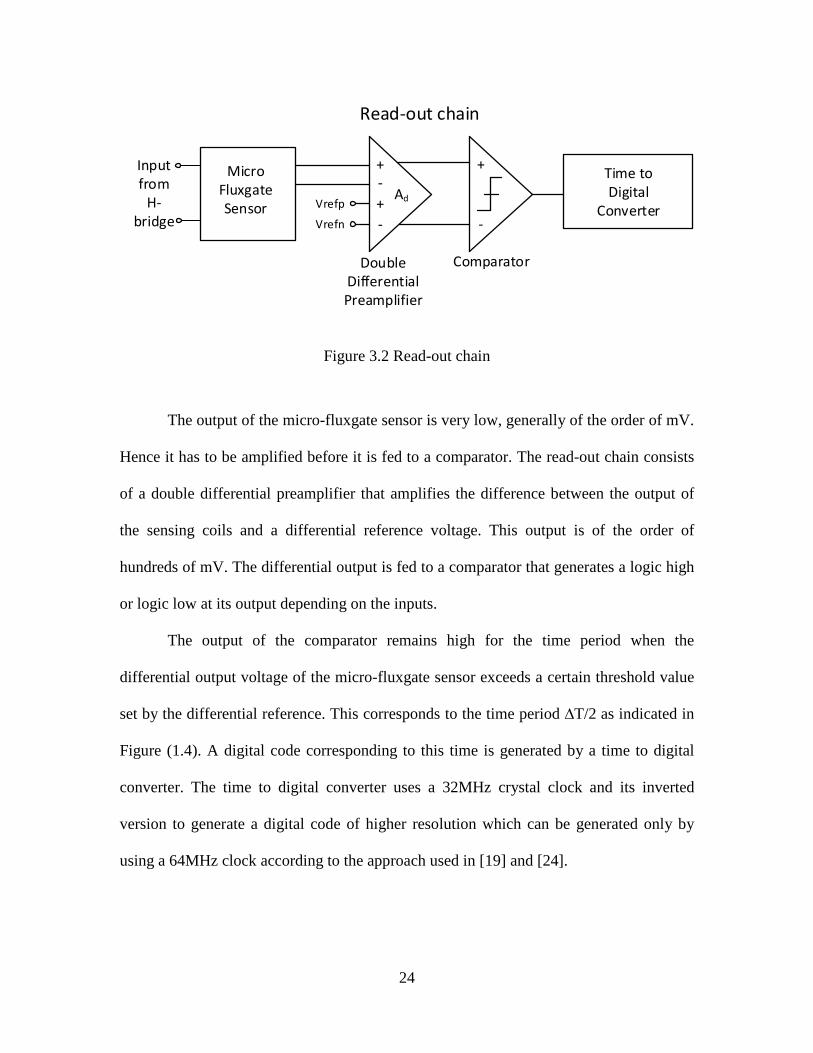
The output of the micro-fluxgate sensor is very low, generally of the order of mV.
Hence it has to be amplified before it is fed to a comparator. The read-out chain consists
of a double differential preamplifier that amplifies the difference between the output of
the sensing coils and a differential reference voltage. This output is of the order of
hundreds of mV. The differential output is fed to a comparator that generates a logic high
or logic low at its output depending on the inputs.
The output of the comparator remains high for the time period when the
differential output voltage of the micro-fluxgate sensor exceeds a certain threshold value
set by the differential reference. This corresponds to the time period ∆T/2 as indicated in
Figure (1.4). A digital code corresponding to this time is generated by a time to digital
converter. The time to digital converter uses a 32MHz crystal clock and its inverted
version to generate a digital code of higher resolution which can be generated only by
using a 64MHz clock according to the approach used in [19] and [24].

25
Some of the salient features of the proposed analog front end are:
1) The use of charge pump to generate a triangular voltage waveform gives reduced
power consumption compared to previous approaches.
2) H-Bridge is used to switch the direction of current flowing into the excitation coil
eliminating the use of symmetric power supply.
3) The read-out circuit is not susceptible to amplitude noise in the output voltage of
the sensor.
4) Digital output is produced without using an ADC.
5) The time to digital converter uses a 32MHz clock and generates digital code that
is as accurate as the digital code generated using a 64MHz clock using previous
approaches in [19] and [24].
3.1 Excitation Circuit
Each block of the excitation circuit is discussed in detail in the following sections.
3.1.1 Charge Pump:
A charge pump consists of two constant current sources which linearly charge or
discharge a capacitor at its output. The current sources are connected to the output or
disconnected from the output using switches. The charge pump used to generate a
triangular voltage waveform is shown in Figure (3.3). The transistors M2 and M3 form a
current source that discharges the output and the transistors M4 and M5 form a current
source used to charge the output. The transistors M1 and M6 are in triode and are used as
switches. The cascode current source formed by M5 and M4 is biased using a wide swing
cascode bias with a dummy switch in the bias circuit which replicates the effect of the

26
switch M6. The cascode current source formed by M2 and M3 is biased using a wide
swing cascode bias with a dummy switch in the bias circuit which replicates the effect of
the switch M1 [20].
VDD
VDD
Vsink
CSET
Ibias
Clk
Clk
Reset
M1
M2
M3
M4
M5
M6
Ip
In
M7
Figure 3.3 Charge Pump
The charge pump shown in Figure (3.3) uses cascode current sources with larger
output impedance to reduce the effect of power supply noise on the output. It employs
source switching which ensures that the transistors M2-M5 are always in saturation
thereby avoiding any peak current that may flow if the transistors M1 and M2 or M4 and
M5 are in triode for some portion of time. The switching time for this charge pump is
also lower due to the fact that the switches M1 and M6 are connected to a single
transistor only.
27
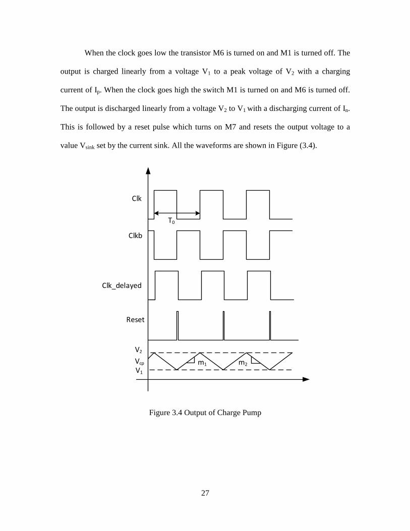
When the clock goes low the transistor M6 is turned on and M1 is turned off. The
output is charged linearly from a voltage V1 to a peak voltage of V2 with a charging
current of Ip. When the clock goes high the switch M1 is turned on and M6 is turned off.
The output is discharged linearly from a voltage V2 to V1 with a discharging current of In.
This is followed by a reset pulse which turns on M7 and resets the output voltage to a
value Vsink set by the current sink. All the waveforms are shown in Figure (3.4).
Clk
Clkb
Clk_delayed
Reset
Vcp
V2
V1
T0
m1 m2
Figure 3.4 Output of Charge Pump
28
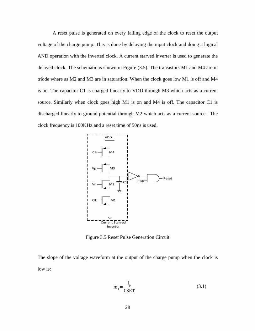
A reset pulse is generated on every falling edge of the clock to reset the output
voltage of the charge pump. This is done by delaying the input clock and doing a logical
AND operation with the inverted clock. A current starved inverter is used to generate the
delayed clock. The schematic is shown in Figure (3.5). The transistors M1 and M4 are in
triode where as M2 and M3 are in saturation. When the clock goes low M1 is off and M4
is on. The capacitor C1 is charged linearly to VDD through M3 which acts as a current
source. Similarly when clock goes high M1 is on and M4 is off. The capacitor C1 is
discharged linearly to ground potential through M2 which acts as a current source. The
clock frequency is 100KHz and a reset time of 50ns is used.
Clk
Clk
Vp
VnClkbC1
VDD
Reset
Current Starved
Inverter
M1
M2
M3
M4
Figure 3.5 Reset Pulse Generation Circuit
The slope of the voltage waveform at the output of the charge pump when the clock is
low is:
p
1
Im =
CSET (3.1)
29
The slope of the voltage waveform at the output of the charge pump when the clock is
high is:
If both the charging current and discharging current are equal then
If there is a mismatch in the currents Ip and In a non-linearity is caused in the
voltage at the output of the charge pump when it is reset. Since this happens for a very
small amount of time (0.5% of the time period) its effect is very small. There will also be
a mismatch in the slopes m1 and m2 which modulates the amplitude of the differential
sensor output. But since phase delay based read-out is done this will not effect the digital
output of the system. The noise in the output voltage of the charge pump due to charge
injection from M7 is partly cancelled because it also effects the voltage Vsink which
subtracted from the voltage at the positive terminal of the resistor RSET as shown in
Figure (3.1). The value of I0 is 5µA and CSET is 40pF.
n
2
Im =
CSET (3.2)
p n 0I =I =I (3.3)
1 2
m =m (3.4)
1 sinkV =V (3.5)
0
2 sink
I TV =V + *
CSET 2 (3.6)
30
3.1.2 Triangular Current Generator
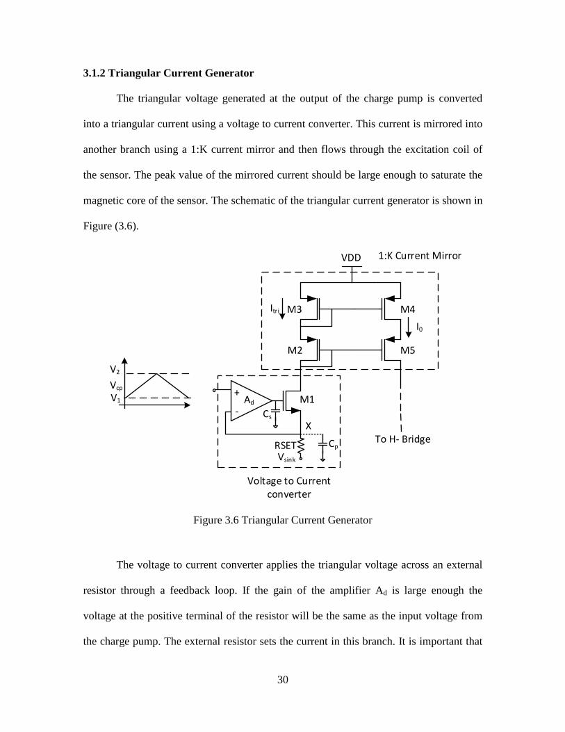
The triangular voltage generated at the output of the charge pump is converted
into a triangular current using a voltage to current converter. This current is mirrored into
another branch using a 1:K current mirror and then flows through the excitation coil of
the sensor. The peak value of the mirrored current should be large enough to saturate the
magnetic core of the sensor. The schematic of the triangular current generator is shown in
Figure (3.6).
+
-M1
M2
M3 M4
M5
RSET
VDD
To H- Bridge
Cs
Cp
Vcp
V2
V1
Voltage to Current
converter
1:K Current Mirror
Vsink
Itri
I0
Ad
X
Figure 3.6 Triangular Current Generator
The voltage to current converter applies the triangular voltage across an external
resistor through a feedback loop. If the gain of the amplifier Ad is large enough the
voltage at the positive terminal of the resistor will be the same as the input voltage from
the charge pump. The external resistor sets the current in this branch. It is important that
31
the excitation current has little variation with temperature so that the output of the sensor
is less dependent on temperature. Since the external resistor can be made to have a very
good temperature coefficient the current Itri exhibits only a little dependence on
temperature. It is also important to have a low offset amplifier so that the voltage across
the resistor actually goes from zero to a peak value and so does the current Itri.
A folded cascode OTA is used to implement the gain stage. The current through
the transistor M1 changes from zero to a peak value of few mA. Hence the gate of M1
has to be modulated to supply this wide range of current. So the output of the amplifier
should have high swing. The amplifier should have good enough gain so that the voltage
at the positive terminal of the resistor RSET is same as the charge pump output voltage.
The unity gain bandwidth of the feedback loop should also be large enough to pass a
considerable number of harmonics of the input voltage. Since an external resistor is used
it will have some parasitic capacitance Cp across it. This forms a pole at a frequency of fp2
given by equation (3.8). In order to stabilize the feedback loop the pole at the output of
the amplifier, given by equation (3.9), should be the dominant pole. This is done by
adding a capacitor Cs at the output of the amplifier.
cp sink
tri
V -VI =
RSET (3.7)
p1
out s
1f =
2πR *C (3.8)
p2
X p
1f =
2πR *C (3.9)
32
Rout is the output impedance of the folded cascode OTA and RX is the impedance seen at
the node X. At higher currents Rx is dominated by the gm of M1 and equals 1/gm1. At
low currents the gm of M1 decreases and Rx is almost equal to RSET. The capacitance Cs
has been chosen such that the feedback loop is stable for all cases. This is verified from
the transient response.
The triangular current generated is mirrored into another branch using a 1:K
current mirror with K=20. A higher value of K is chosen so as to reduce the bias current.
A cascode current mirror is used so as to provide large output impedance. It also helps in
reducing the effect of power supply noise on the excitation current. The transistors M2-
M5 should be in saturation region for all portion of time. Hence these devices are usually
very big and consume a major portion of area. It is important to match the transistors in
the current mirror using proper layout techniques as discussed later. Since the resistor
RSET is external it can be adjusted to get the required excitation current to saturate the
magnetic core. The nominal value of RSET is 230Ω.
3.1.3 Current Sink
The voltage at the negative terminal of the resistance RSET has to be maintained
fixed at Vsink so that the effective voltage across RSET is a triangular wave going from
zero to a certain peak voltage equal to V2-Vsink . And hence the current through the
resistor also goes from zero to a peak value linearly. Since the current through this branch
is of the order of a few mA the circuit which sinks this current should have extremely low
output impedance. A current sink is employed for this purpose.

33
The schematic of the current sink is shown in Figure (3.7). The impedance
looking into the node Y is given as:
-
+VsinkCs
C0
M10
To RSET
Y
Ad
Figure 3.7 Current Sink
A folded cascode OTA followed by a level shifter stage is used for implementing
the gain stage. The voltage Vsink should be greater than the overdrive voltage of the
PMOS transistor M1. Another factor in choosing Vsink is the minimum voltage required to
be maintained at the output of the charge pump. According to these parameters Vsink is set
to be 1.5V. The feedback loop has a finite bandwidth and hence an external capacitance
of 200pF to ground is used to reduce the variation in the voltage at node Y. The capacitor
Cs is added for stability. The folded cascode OTA used here is similar to the one used in
the voltage to current converter of triangular current generator. This would reduce the
effect of OTA offsets on the excitation current.
10
Y
d
(1/gm )R =
1+A (3.10)

34
3.1.4 H-Bridge
The current supplied by the current mirror is a triangular current that flows from
supply to ground through the excitation coil. But the fluxgate sensor needs to be excited
with an alternating (AC) current. Hence an H-bridge is used to change the direction of the
current through the excitation coil. The schematic of the H-bridge is shown in Figure
(3.8).
M6
M8
M7
M9
H HbRs Ls
Excitation
Coil
From Current Mirror
DFF
Q
Qb
Clk
D
Clkb H
Hb
Iexc
I0
Figure 3.8 H-Bridge Circuit
The H-bridge consists of two CMOS inverter like structures. The current flows in
one direction or the other depending on which transistors are turned on. The signals H
and Hb which drive the gates of the transistor M6-M9 are should have half of the
frequency of the clock that drives the charge pump. Hence a frequency divider with
divide by two ratio is used to obtain these signals. The signal H remains high for one
clock cycle of the charge pump clock and remains low for the next clock cycle. The
signal Hb is an inverted version of the signal H.
35
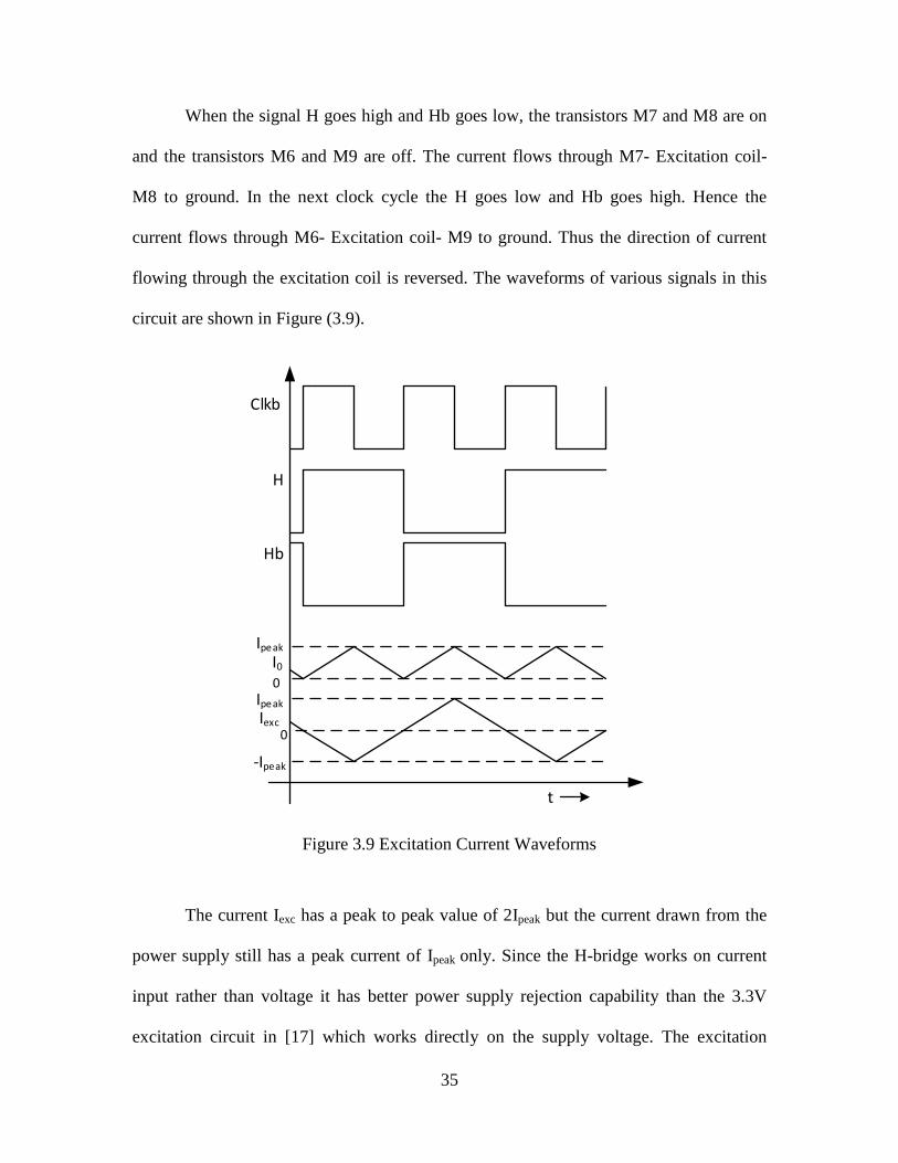
When the signal H goes high and Hb goes low, the transistors M7 and M8 are on
and the transistors M6 and M9 are off. The current flows through M7- Excitation coil-
M8 to ground. In the next clock cycle the H goes low and Hb goes high. Hence the
current flows through M6- Excitation coil- M9 to ground. Thus the direction of current
flowing through the excitation coil is reversed. The waveforms of various signals in this
circuit are shown in Figure (3.9).
Clkb
H
Hb
0
I0
Ipeak
0
Ipeak
-Ipeak
t
Iexc
Figure 3.9 Excitation Current Waveforms
The current Iexc has a peak to peak value of 2Ipeak but the current drawn from the
power supply still has a peak current of Ipeak only. Since the H-bridge works on current
input rather than voltage it has better power supply rejection capability than the 3.3V
excitation circuit in [17] which works directly on the supply voltage. The excitation

36
current will have some spikes at the zero crossings due to the inductive nature of the
excitation coil and some parasitic capacitance. This will cause a spike in the voltage at
the outputs of individual sensing coils but the differential output voltage will still be
clean. This is because all disturbances in the excitation current around zero will appear as
common mode noise to the sensor and will be suppressed in the differential output.
3.2 Read-out Chain
In order to measure the phase delay between two consecutive pulses at the output
of the fluxgate sensor as described in Chapter 1, we need to process the signals through a
triggering circuit like comparator. Micro-fluxgate sensors have noise at the point where
the differential output voltage is supposed to be zero. Hence it is desired to have a circuit
which is triggered only when the differential voltage exceeds a certain threshold value.
The amplitude of the output voltage is usually of the order of mV. Hence it is required to
amplify this signal by passing it through a preamplifier before it is given to a comparator.
After the comparator a time to digital converter is used to produce an output digital code
proportional to the pulse width of the output of the comparator.
3.2.1 Double Differential Preamplifier
The double differential preamplifier forms the first stage of the read-out circuit.
The schematic of the double differential preamplifier used is shown in Figure (3.10) [25].
37
VDD
R1
R2
Vcmref
Vinp Vrefp Vrefn Vinn
Voutn Voutp
M1 M2 M3 M4
M5M6
M7M8
M9 M10
M11 M12M13
M14
Ib
Figure 3.10 Double Differential Preamplifier
The double differential preamplifier is fully differential and gives an output (Voutp-
Voutn) which crosses zero when the differential input (Vinp-Vinm) crosses the
differential threshold (Vrefp-Vrem). The small signal gain is given as:
In order to obtain a good gain active load is used in the preamplifier. This
necessitates the use of Common Mode Feedback (CMFB) to set the output dc level
reliably. The transistors M11-M13 are in triode. The resistance of these transistors is
d 1 1 9A =gm *(ro ||ro ) (3.11)
(3.12) d
Voutp-Voutn=A ((Vinp-Vinn)-(Vrefp-Vrefn))
38
adjusted such that ID9 and ID10 exactly balance ID5 and ID6 respectively. If we assume
that the (W/L) of M14 is equal to the (W/L) of M9 and M10 then the currents through all
of these transistors will be equal. Hence if (W/L) of M13 equals the (W/L) of M11 and
M12 the currents ID14 and ID9, 10 track each other. This sets the output common mode
equal to Vcmref. In practice Vds of M14 and M9 are not equal and this would result in a
finite error. The output swing is also limited by the transistors M11 and M12 as the
output voltage cannot go beyond VDD-|Vth11,12|. But these two limitations do not have a
major effect on the current read- out circuit.
It is important to have good matching between the input devices to have low offsets.
However offsets less than a mV do not have a significant impact because the output of
the sensor has a relatively small rise time.
3.2.2 Comparator
The output of the preamplifier is of the order of a few hundred mV. This is given
as input to a comparator stage which produces proper logic levels at it its output. The
comparator used in the read- out circuit is shown in Figure (3.11) [20].
2
1 2
RVcmref= VDD
R +R (3.13)
Voutp+ Voutn
Voutdc = ( )2
(3.14)
13 11,12 14 9,10
W W W WVoutdc = Vcmref if = and =
L L L L
(3.15)

39
Ib
VDD
Vinp VinmM1 M2
M3 M4 M5 M6
M7 M8 M9
M10 M11
M12
VBP
Vout
VDD
Rif
Figure 3.11 Current-mode Comparator
The comparator is a current mode comparator. Current mode comparators have
higher speed and larger bandwidth. They also require lower voltage headroom to operate
than those operating in voltage mode. The comparator consists of a transconductance
stage followed by a current subtractor, two current-source inverting amplifiers and a
CMOS inverter. The differential input voltage produces a proportional difference in the
currents flowing through the transistors M1 and M2. These currents are mirrored into M5
and M6. The difference in the currents through M6 and M5 flows into the first current
source amplifier. The first current-source amplifier employs resistive feedback to reduce
the input and output impedances. The signal is passed through another current-source
amplifier and a CMOS inverter to produce a signal with proper logic levels at the output.
40
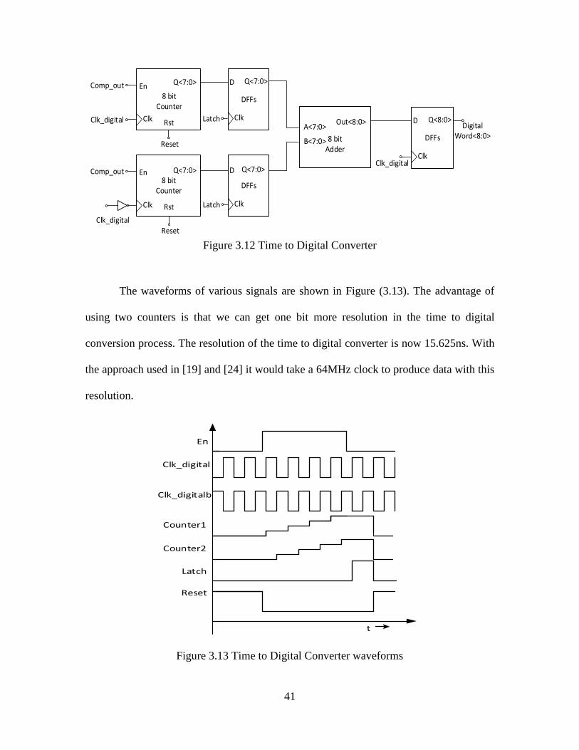
3.2.3 Time to Digital Converter
The output of the comparator has a certain pulse width with proper logic levels. A
digital word corresponding to this pulse width is produced by a time to digital converter.
Conventional fluxgate sensors have very low excitation frequencies of the order of Hz
and hence a counter run at a few tens of MHz would give good resolution. Micro-fluxgate
sensors have excitation frequencies of the order of few hundreds of kHz. Hence time to
digital converter also forms a crucial part of the read-out chain.
The time to digital converter used is shown in Figure (3.12). It uses two
synchronous counters which run on a 32MHz clock and its inverted version. The output
of the comparator is given as an enable to the counters. When enable goes high both the
counters start counting. When the enable goes low the counters retain the count. After
this the Latch signal goes high for one clock cycle of the 32MHz clock. The data in the
counters is latched into a bank of D Flip-flops. The Latch signal is followed by reset
signal which resets the counters. The digital codes in the D Flip-flops are added using an
8-bit adder. The resulting code corresponds to the pulse width of the output of the
comparator and hence is proportional to the external magnetic field. For each enable
pulse the digital code is updated.
41
En
Clk
Q<7:0>
En
Clk
Q<7:0>
D
Clk
Clk
D
A<7:0>
B<7:0>
Out<8:0>
Q<7:0>
Q<7:0>
D
Clk
Q<8:0>
Comp_out
Comp_out
Clk_digital
Clk_digital
Rst
Rst
Reset
Reset
Latch
Latch
8 bit
CounterDFFs
DFFs8 bit
Counter
8 bit
Adder
DFFs
Clk_digital
Digital
Word<8:0>
Figure 3.12 Time to Digital Converter
The waveforms of various signals are shown in Figure (3.13). The advantage of
using two counters is that we can get one bit more resolution in the time to digital
conversion process. The resolution of the time to digital converter is now 15.625ns. With
the approach used in [19] and [24] it would take a 64MHz clock to produce data with this
resolution.
En
Clk_digital
Clk_digitalb
Counter1
Counter2
Latch
Reset
t
Figure 3.13 Time to Digital Converter waveforms
42
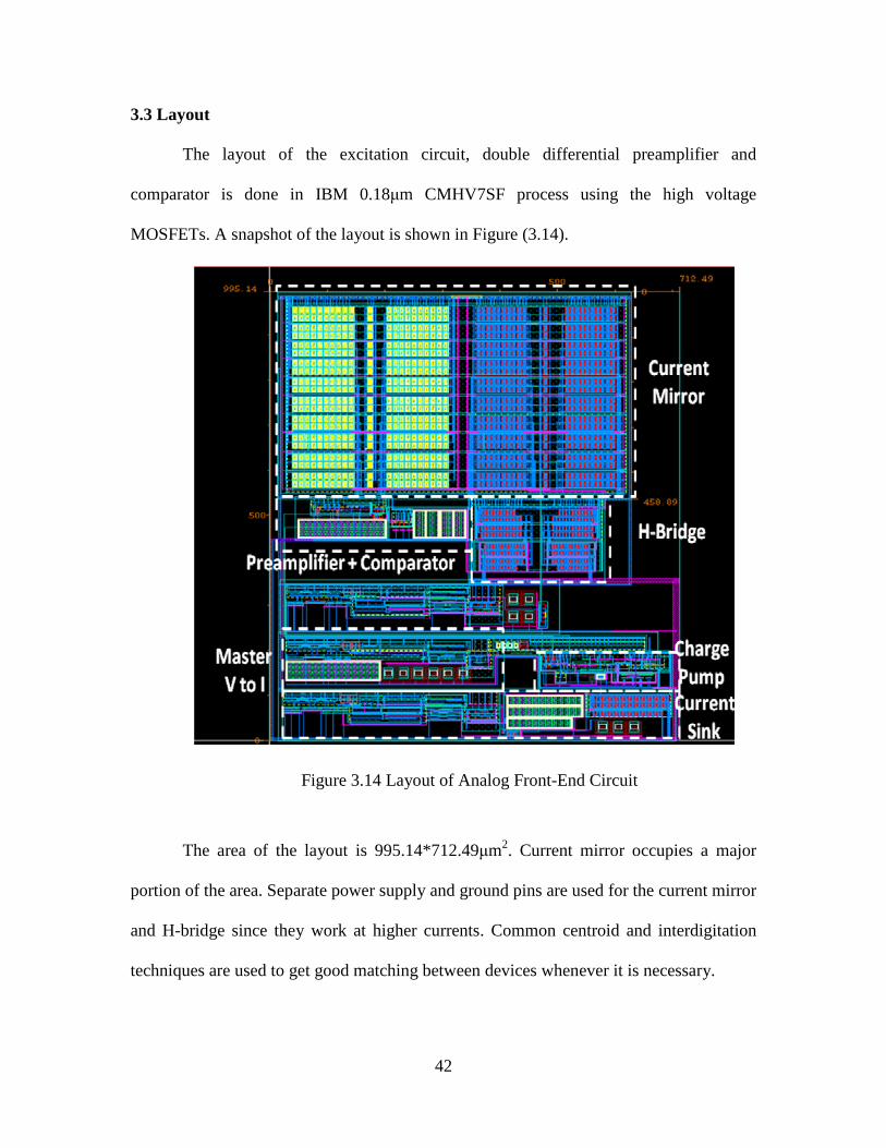
3.3 Layout
The layout of the excitation circuit, double differential preamplifier and
comparator is done in IBM 0.18µm CMHV7SF process using the high voltage
MOSFETs. A snapshot of the layout is shown in Figure (3.14).
Figure 3.14 Layout of Analog Front-End Circuit
The area of the layout is 995.14*712.49µm2. Current mirror occupies a major
portion of the area. Separate power supply and ground pins are used for the current mirror
and H-bridge since they work at higher currents. Common centroid and interdigitation
techniques are used to get good matching between devices whenever it is necessary.
43
Chapter 4
RESULTS
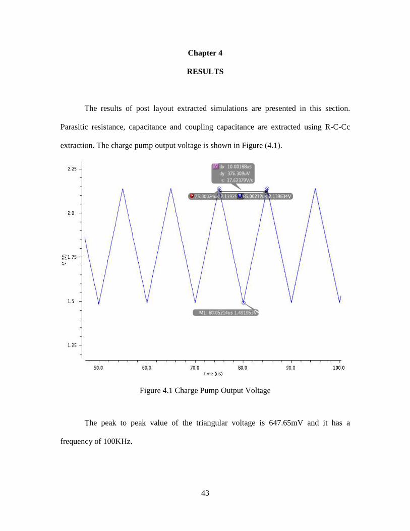
The results of post layout extracted simulations are presented in this section.
Parasitic resistance, capacitance and coupling capacitance are extracted using R-C-Cc
extraction. The charge pump output voltage is shown in Figure (4.1).
Figure 4.1 Charge Pump Output Voltage
The peak to peak value of the triangular voltage is 647.65mV and it has a
frequency of 100KHz.
44
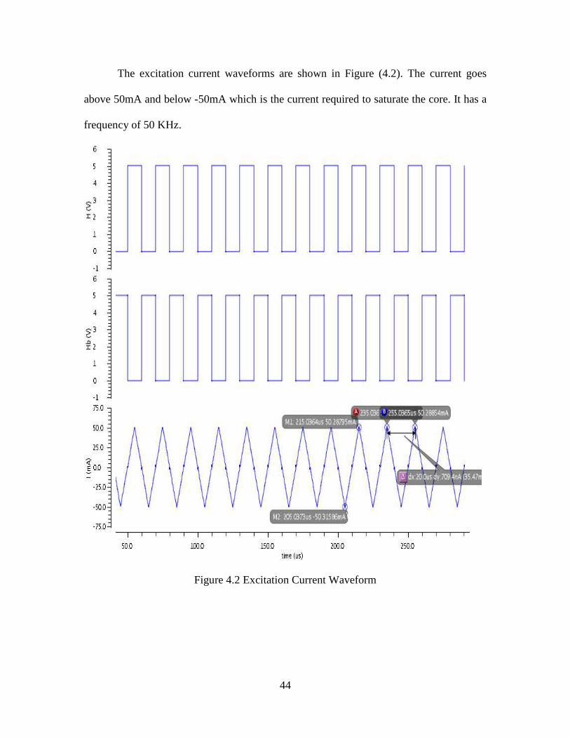
The excitation current waveforms are shown in Figure (4.2). The current goes
above 50mA and below -50mA which is the current required to saturate the core. It has a
frequency of 50 KHz.
Figure 4.2 Excitation Current Waveform
45
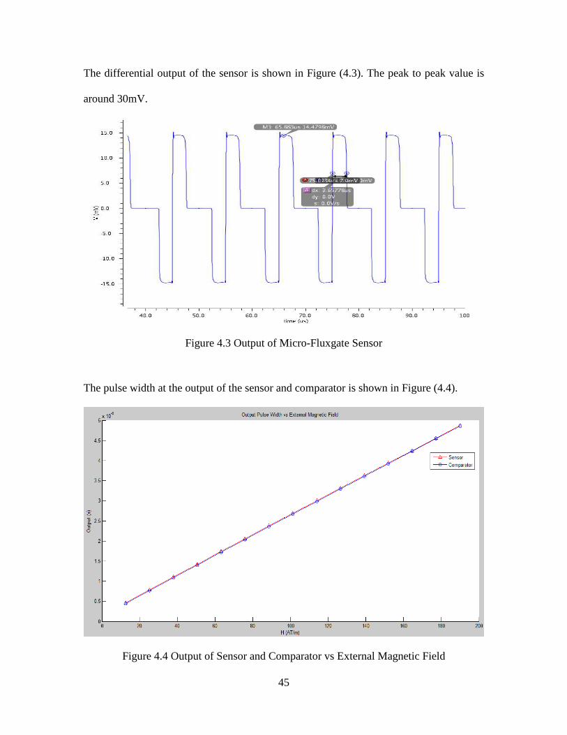
The differential output of the sensor is shown in Figure (4.3). The peak to peak value is
around 30mV.
Figure 4.3 Output of Micro-Fluxgate Sensor
The pulse width at the output of the sensor and comparator is shown in Figure (4.4).
Figure 4.4 Output of Sensor and Comparator vs External Magnetic Field
46
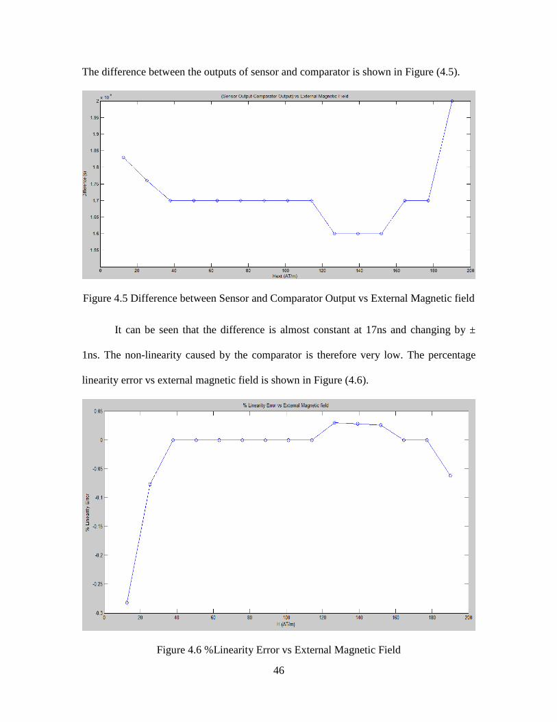
The difference between the outputs of sensor and comparator is shown in Figure (4.5).
Figure 4.5 Difference between Sensor and Comparator Output vs External Magnetic field
It can be seen that the difference is almost constant at 17ns and changing by ±
1ns. The non-linearity caused by the comparator is therefore very low. The percentage
linearity error vs external magnetic field is shown in Figure (4.6).
Figure 4.6 %Linearity Error vs External Magnetic Field

47
The digital output of the system vs external magnetic field is shown in Figure (4.7).
Figure 4.7 Digital Output vs External Magnetic Field
Table 3.1 summarizes the key specifications of the developed analog front-end circuit.
Parameter Value
Process IBM CMOS 0.18µm
RMS Power Consumption of AFE (excludes
the power delivered to the sensor)
5.025mW
%Linearity Error at the output of comparator -0.282%
Resolution of time to digital converter 15.625ns with 32MHz clock
Layout area 995.14*712.49µm2
Table 4.1 Key Specifications of Developed Analog Front-End

48
Chapter 5
CONCLUSION
A new analog front-end circuit for micro-fluxgate sensors is developed. Charge
pump based excitation circuit is used to reduce the power consumption of the excitation
circuit. An H-bridge is used to reverse the direction of current through the excitation coil
without the use of symmetric power supply. Phase delay based read-out technique is
implemented. It produces a digital output without using an ADC. The read-out circuit is
immune to amplitude noise and hence it is best suited for use for micro-fluxgate sensors
whose output voltage is much lower. Phase delay based read-out circuit also has low
power.
The analog front-end circuit is simulated with a SPICE model of micro-fluxgate
sensor and excellent linearity in the output is obtained. An offset of about 17ns is
produced at the output due to asymmetric rise and fall times at the output of the sensor.
But it can be easily calibrated. The time to digital converter produces an output with
15.625ns resolution using a 32MHz clock. The analog front end circuit consumes
5.025mW of power excluding the power supplied to the micro-fluxgate sensor and the
bias current to the current mirror. This is much lower compared to the power
consumption of the state-of-the-art analog front end circuits presented in this thesis. The
layout has an area of 995.14*712.49µm2. The area can be further reduced depending on
the current consumption of the sensor.
49
REFERENCES
[1] Pavel Ripka, Advances in fluxgate sensors, Sensors and Actuators A: Physical, Volume 106, Issues 1–3, 15 September 2003
[2] Velasco-Quesada, G.; Román-Lumbreras, M.; Conesa-Roca, A.; Jeréz, F., "Design of a Low-Consumption Fluxgate Transducer for High-Current Measurement Applications," Sensors Journal, IEEE , vol.11, no.2, pp.280,287, Feb. 2011
[3] Florian Kaluza, Angelika Grüger, Heinrich Grüger, New and future applications of fluxgate sensors, Sensors and Actuators A: Physical, Volume 106, Issues 1–3, 15 September 2003
[4] Major, R. V., "Current measurement with magnetic sensors," Magnetic Materials for Sensors and Actuators (Digest No. 1994/183), IEE Colloquium on , vol., no., pp.5/1,5/3, 11 Oct 1994
[5] Baschirotto, A.; Dallago, E.; Malcovati, P.; Marchesi, M.; Venchi, G., "From a PCB Fluxgate to an integrated micro Fluxgate magnetic sensor," Instrumentation and Measurement Technology Conference, 2005. IMTC 2005. Proceedings of the IEEE , vol.3, no., pp.1756,1760, 16-19 May 2005
[6] Baschirotto, A.; Dallago, E.; Malcovati, P.; Marchesi, M.; Venchi, G., "Fluxgate magnetic sensor in PCB technology," Instrumentation and Measurement Technology Conference, 2004. IMTC 04. Proceedings of the 21st IEEE , vol.2, no., pp.808,812 Vol.2, 18-20 May 2004
[7] Baschirotto, A.; Dallago, E.; Ferragina, V.; Ferri, M.; Grassi, M.; Malcovati, P.; Marchesi, M.; Melissano, E.; Morelli, M.; Rossini, A.; Ruzza, S.; Siciliano, P.; Venchi, G., "A CMOS 2D Micro-Fluxgate Earth Magnetic Field Sensor with Digital Output," Solid-State Circuits Conference, 2007. ISSCC 2007. Digest of Technical Papers. IEEE International , vol., no., pp.390,610, 11-15 Feb. 2007
[8] Jian Lei, Chong Lei, Yong Zhou, Fabrication and characterization of a new MEMS fluxgate sensor with nanocrystalline magnetic core, Measurement, Volume 45, Issue 3, April 2012
[9] Maria Teresa Todaro, Leonardo Sileo and Massimo De Vittorio (2012). Magnetic Field Sensors Based on Microelectromechanical Systems (MEMS) Technology, Magnetic Sensors - Principles and Applications, Dr Kevin Kuang (Ed)
50
[10] Ripka, P. (2001). Magnetic sensors and magnetometers. Boston: Artech House
[11] Go"pel, W., J. Hesse, J. N. Zemel, R. Boll, and K. J. Overshott. 1989. Sensors: a comprehensive survey Vol. 5, Vol. 5. Weinheim: VCH
[12] Gupta, S.; Ahn, Chong H.; Park, J., II, "Electromagnetic modeling and harmonic analysis of micro-machined ring-type magnetic fluxgate sensor using SPICE," Sensors, 2003. Proceedings of IEEE , vol.1, no., pp.622,625 Vol.1, 22-24 Oct. 2003
[13] Gupta, Sukirti. "Simulation and Optimization of Micromachined Magnetic Fluxgate Sensors." Electronic Thesis or Dissertation. University of Cincinnati, 2002
[14] Ripka, P.; San On Choi; Tipek, A.; Kawahito, S.; Ishida, M., "Pulse excitation of micro-fluxgate sensors," Magnetics, IEEE Transactions on , vol.37, no.4, pp.1998,2000, Jul 2001
[15] Baschirotto, A.; Borghetti, F.; Dallago, E.; Malcovati, P.; Marchesi, M.; Venchi, G., "A CMOS front-end circuit for integrated fluxgate magnetic sensors," Circuits and Systems, 2006. ISCAS 2006. Proceedings. 2006 IEEE International Symposium on , vol., no., pp.4 pp.,4406, 21-24 May 2006
[16] Baschirotto, A.; Dallago, E.; Malcovati, P.; Marchesi, M.; Melissano, E.; Morelli, M.; Siciliano, P.; Venchi, G., "An Integrated Micro-Fluxgate Magnetic Sensor With Front-End Circuitry," Instrumentation and Measurement, IEEE Transactions on , vol.58, no.9, pp.3269,3275, Sept. 2009
[17] Ferri, M.; Surano, A.; Rossini, A.; Malcovati, P.; Dallago, E.; Baschirotto, A., "Low-voltage fluxgate magnetic current sensor interface circuit with digital output for portable applications," Sensors, 2009 IEEE , vol., no., pp.79,82, 25-28 Oct. 2009
[18] R Gottfried-Gottfried, W Budde, R Jähne, H Kück, B Sauer, S Ulbricht, U Wende, A miniaturized magnetic-field sensor system consisting of a planar fluxgate sensor and a CMOS readout circuitry, Sensors and Actuators A: Physical, Volume 54, Issues 1–3, June 1996
[19] P.D Dimitropoulos, J.N Avaritsiotis, E Hristoforou, Boosting the performance of miniature fluxgates with novel signal extraction techniques, Sensors and Actuators A: Physical, Volume 90, Issues 1–2, 1 May 2001
[20] Woogeun Rhee, "Design of high-performance CMOS charge pumps in phase-locked loops," Circuits and Systems, 1999. ISCAS '99. Proceedings of the 1999 IEEE International Symposium on , vol.2, no., pp.545,548 vol.2, Jul 1999
51
[21] Byung-Moo Min; Soo-Won Kim, "High performance CMOS current comparator using resistive feedback network," Electronics Letters , vol.34, no.22, pp.2074,2076, 29 Oct 1998
[22] Marchesi, M.: Fluxgate Magnetic Sensor System for Electronic Compass, Dissertation, Universita’ Degli Studi di Pavia
[23] Ferri, M.:Integrated magnetic sensor interface circuits and photovoltaic energy harvester systems, Dissertation, Universita’ Degli Studi di Pavia
[24] Baglio, S.; Sacco, V.; Bulsara, A., "Read-out circuit in RT-fluxgate," Circuits and Systems, 2005. ISCAS 2005. IEEE International Symposium on , vol., no., pp.5910,5913 Vol. 6, 23-26 May 2005
[25] Razavi, Behzad. "Design of Analog CMOS Integrated Circuits."