Fully Integrated, 8-Channel Ultrasound Analog Front End with
110
SPI LNA VCAT 0 to -40 dB SPI Logic 16X CLKP IN PGA 24, 30dB 3 rd LP Filter 10, 15, 20, 30 MHz 16 Phases Generator CW Mixer Summing Amplifier/ Filter 16X CLKN 1X CLK CW I/Q Vout AFE5809 with Demodulator 1 of 8 Channels 14 Bit ADC LVDS OUT Reference Reference Differential TGC Vcntl EXT/INT REFM/P Digital DeMod & LP Filter LVDS Serializer Logic Control DeMod Control Product Folder Sample & Buy Technical Documents Tools & Software Support & Community AFE5809 SLOS738E – SEPTEMBER 2012 – REVISED AUGUST 2015 AFE5809 Fully Integrated, 8-Channel Ultrasound Analog Front End With Passive CW Mixer, and Digital I/Q Demodulator, 0.75 nV/rtHz, 14, 12-Bit, 65 MSPS, 158 mW/CH 1 Features • Fast and Consistent Overload Recovery • Passive Mixer for Continuous Wave Doppler 1• 8-Channel Complete Analog Front-End (CWD) – LNA, VCAT, PGA, LPF, ADC, and CW Mixer – Low Close-in Phase Noise –156 dBc/Hz at 1 • Programmable Gain Low-Noise Amplifier (LNA) kHz off 2.5-MHz Carrier – 24-, 18-, 12-dB Gain – Phase Resolution of 1/16λ – 0.25-, 0.5-, 1-V PP Linear Input Range – Support 16×, 8×, 4×, and 1× CW Clocks – 0.63-, 0.7-, 0.9-nV/rtHz Input Referred Noise – 12-dB Suppression on Third and Fifth – Programmable Active Termination Harmonics • 40-dB Low-Noise Voltage Controlled Attenuator – Flexible Input Clocks (VCAT) • Small Package: 15 mm × 9 mm, 135-BGA • 24-/30-dB Programmable Gain Amplifier (PGA) • Third-Order Linear Phase Low-Pass Filter (LPF) 2 Applications – 10, 15, 20, 30 MHz • Medical Ultrasound Imaging • 14-Bit Analog-to-Digital Converter (ADC) • Nondestructive Evaluation Equipments – 77 dBFS SNR at 65 MSPS • Sonar Applications – LVDS Outputs • Noise, Power Optimizations (Without Digital 3 Description Demodulator) The AFE5809 device is a highly-integrated analog front-end (AFE) solution specifically designed for – 158 mW/CH at 0.75 nV/rtHz, 65 MSPS ultrasound systems in which high performance and – 101 mW/CH at 1.1 nV/rtHz, 40 MSPS small size are required. The AFE5809 device – 80 mW/CH at CW Mode integrates a complete time-gain-control (TGC) imaging path and a CWD path. The device also • Excellent Device-to-Device Gain Matching enables users to select one of various power and – ±0.5 dB (Typical) and ±1 dB (Maximum) noise combinations to optimize system performance. • Digital I/Q Demodulator after ADC Therefore, the AFE5809 device is a suitable – Wide Range Demodulation Frequency ultrasound AFE solution not only for high-end systems, but also for portable ones. – <1 kHz Frequency Resolution – Decimation Filter Factor M = 1 to 32 Device Information (1) – 16xM Tap FIR Decimation Filter PART NUMBER PACKAGE BODY SIZE (NOM) – LVDS Rate Reduction after Demodulation AFE5809 NFBGA (135) 15.00 mm × 9.00 mm – On-Chip RAM With 32 Preset Profiles (1) For all available packages, see the orderable addendum at the end of the data sheet. • Low Harmonic Distortion • Low-Frequency Sonar Signal Processing Block Diagram 1 An IMPORTANT NOTICE at the end of this data sheet addresses availability, warranty, changes, use in safety-critical applications, intellectual property matters and other important disclaimers. PRODUCTION DATA.
Transcript of Fully Integrated, 8-Channel Ultrasound Analog Front End with

SPI
LNAVCAT0 to -40 dB
SPI Logic
16X CLKP
INPGA
24, 30dB
3rd
LP Filter10, 15, 20, 30
MHz
16 Phases
GeneratorCW Mixer Summing
Amplifier/ Filter16X CLKN
1X CLK
CW I/Q Vout
AFE5809 with Demodulator1 of 8 Channels
14 Bit
ADCLVDS
OUT
ReferenceReference
DifferentialTGC Vcntl
EXT/INTREFM/P
DigitalDeMod &LP Filter
LVDSSerializer
Logic
Control
DeModControl
Product
Folder
Sample &Buy
Technical
Documents
Tools &
Software
Support &Community
AFE5809SLOS738E –SEPTEMBER 2012–REVISED AUGUST 2015
AFE5809 Fully Integrated, 8-Channel Ultrasound Analog Front End With Passive CWMixer, and Digital I/Q Demodulator, 0.75 nV/rtHz, 14, 12-Bit, 65 MSPS, 158 mW/CH
1 Features • Fast and Consistent Overload Recovery• Passive Mixer for Continuous Wave Doppler
1• 8-Channel Complete Analog Front-End(CWD)– LNA, VCAT, PGA, LPF, ADC, and CW Mixer– Low Close-in Phase Noise –156 dBc/Hz at 1• Programmable Gain Low-Noise Amplifier (LNA)
kHz off 2.5-MHz Carrier– 24-, 18-, 12-dB Gain– Phase Resolution of 1/16λ– 0.25-, 0.5-, 1-VPP Linear Input Range– Support 16×, 8×, 4×, and 1× CW Clocks– 0.63-, 0.7-, 0.9-nV/rtHz Input Referred Noise– 12-dB Suppression on Third and Fifth– Programmable Active Termination Harmonics
• 40-dB Low-Noise Voltage Controlled Attenuator – Flexible Input Clocks(VCAT)• Small Package: 15 mm × 9 mm, 135-BGA• 24-/30-dB Programmable Gain Amplifier (PGA)
• Third-Order Linear Phase Low-Pass Filter (LPF) 2 Applications– 10, 15, 20, 30 MHz • Medical Ultrasound Imaging
• 14-Bit Analog-to-Digital Converter (ADC) • Nondestructive Evaluation Equipments– 77 dBFS SNR at 65 MSPS • Sonar Applications– LVDS Outputs
• Noise, Power Optimizations (Without Digital 3 DescriptionDemodulator) The AFE5809 device is a highly-integrated analog
front-end (AFE) solution specifically designed for– 158 mW/CH at 0.75 nV/rtHz, 65 MSPSultrasound systems in which high performance and– 101 mW/CH at 1.1 nV/rtHz, 40 MSPS small size are required. The AFE5809 device
– 80 mW/CH at CW Mode integrates a complete time-gain-control (TGC)imaging path and a CWD path. The device also• Excellent Device-to-Device Gain Matchingenables users to select one of various power and– ±0.5 dB (Typical) and ±1 dB (Maximum) noise combinations to optimize system performance.
• Digital I/Q Demodulator after ADC Therefore, the AFE5809 device is a suitable– Wide Range Demodulation Frequency ultrasound AFE solution not only for high-end
systems, but also for portable ones.– <1 kHz Frequency Resolution– Decimation Filter Factor M = 1 to 32 Device Information(1)
– 16xM Tap FIR Decimation Filter PART NUMBER PACKAGE BODY SIZE (NOM)– LVDS Rate Reduction after Demodulation AFE5809 NFBGA (135) 15.00 mm × 9.00 mm– On-Chip RAM With 32 Preset Profiles (1) For all available packages, see the orderable addendum at
the end of the data sheet.• Low Harmonic Distortion• Low-Frequency Sonar Signal Processing
Block Diagram
1
An IMPORTANT NOTICE at the end of this data sheet addresses availability, warranty, changes, use in safety-critical applications,intellectual property matters and other important disclaimers. PRODUCTION DATA.

AFE5809SLOS738E –SEPTEMBER 2012–REVISED AUGUST 2015 www.ti.com
Table of Contents8.6 Register Maps ......................................................... 521 Features .................................................................. 1
9 Application and Implementation ........................ 812 Applications ........................................................... 19.1 Application Information............................................ 813 Description ............................................................. 19.2 Typical Application .................................................. 824 Revision History..................................................... 29.3 System Example ..................................................... 965 Description (continued)......................................... 69.4 Do's and Don'ts....................................................... 986 Pin Configuration and Functions ......................... 7
10 Power Supply Recommendations ..................... 997 Specifications....................................................... 1010.1 Power/Performance Optimization ......................... 997.1 Absolute Maximum Ratings .................................... 1010.2 Power Management Priority................................ 1007.2 ESD Ratings............................................................ 1110.3 Partial Power-Up and Power-Down Mode .......... 1007.3 Recommended Operating Conditions..................... 1110.4 Complete Power-Down Mode ............................. 1007.4 Thermal Information ................................................ 1110.5 Power Saving in CW Mode................................. 1017.5 Electrical Characteristics......................................... 12
11 Layout................................................................. 1017.6 Digital Demodulator Electrical Characteristics ........ 1611.1 Layout Guidelines ............................................... 1017.7 Digital Characteristics ............................................. 1711.2 Layout Example .................................................. 1027.8 Switching Characteristics ........................................ 18
12 Device and Documentation Support ............... 1067.9 SPI Switching Characteristics ................................. 1812.1 Device Support.................................................... 1067.10 Output Interface Timing Requirements (14-bit)..... 1912.2 Documentation Support ...................................... 1067.11 Typical Characteristics .......................................... 2112.3 Community Resources........................................ 1068 Detailed Description ............................................ 3112.4 Trademarks ......................................................... 1068.1 Overview ................................................................. 3112.5 Electrostatic Discharge Caution.......................... 1068.2 Functional Block Diagram ....................................... 3112.6 Glossary .............................................................. 1068.3 Feature Description................................................. 32
13 Mechanical, Packaging, and Orderable8.4 Device Functional Modes........................................ 48Information ......................................................... 1068.5 Programming........................................................... 48
4 Revision HistoryNOTE: Page numbers for previous revisions may differ from page numbers in the current version.
Changes from Revision D (January 2014) to Revision E Page
• Added ESD Ratings table, Feature Description section, Device Functional Modes, Application and Implementationsection, Power Supply Recommendations section, Layout section, Device and Documentation Support section, andMechanical, Packaging, and Orderable Information section ................................................................................................. 1
• Changed N4 and N6 to " When LDO_EN L4 = 1.8 V, demodulator digital power supply generated internally. Thesetwo pins should be separated on the PCB and decoupled respectively with 0.1-µF capacitors. When LDO_ENL4=DVSS, the internal LDOs are disabled. External higher performance 1.4-V supply can be applied to N4 and N6for minimizing digital noise emission. " .................................................................................................................................. 9
• Changed L6 pin description to " Enable/Disable AFE's internal LDO regulators. When it is tied to 1.8-V DVDD orLogic "1", AFE's internal LDO is enabled. When it is tied to DVSS or Logic "0", AFE's internal LDO is disabled andexternal 1.4V supply can be applied at N4 and N6 pins, that is, DVDD_LDO1, DVDD_LDO2. " ......................................... 9
• Changed M6 pin description to "Sets the internal LDO votlage. Logic "1" or tie to 1.8-V DVDD sets the LDO outputas 1.4V. It can be tied to DVSS when the internal LDO is disabled. " .................................................................................. 9
• Added a note to pin H8 "When the complete power-down mode is enabled, the digital demodulator may loseregister settings. Therefore it is required to reconfigure the demodulator registers, filter coefficient memory andprofile memory after existing the complete power-down mode. " ......................................................................................... 9
• Added a note to pin L7 "Note: TX_SYNC signal must be synchronized with ADC CLK. Typically pulse repetitionfrequency (PRF) signal can be used for TX_SYNC_IN. " ................................................................................................... 10
• Added "DVDD_LDO1/2 (external supplied)" in Recommended Operating Conditions ........................................................ 11• Added LDO_EN VIH, VIL,IIH,IIL in Digital Demodulator Electrical Characteristics .................................................................. 16• Deleted "(for output data and frame clock)" ......................................................................................................................... 19• Added a note "TI recommends to synchronize SCLK to ADC CLK... " ............................................................................... 49• Added a note to Register 0 [0]"Register 0 is a write only register." .................................................................................... 52
2 Submit Documentation Feedback Copyright © 2012–2015, Texas Instruments Incorporated
Product Folder Links: AFE5809

AFE5809www.ti.com SLOS738E –SEPTEMBER 2012–REVISED AUGUST 2015
Revision History (continued)• Added a note to Register 0[1] "When this bit is set to 0, device will always operate in write mode; and when it is set
to 1, device will be in read mode. Multiple reading or writing events can be performed when this bit is set to 1 or 0correspondingly. Register 0 is a write only register." .......................................................................................................... 52
• Added a note "When the complete power-down mode is enabled, the digital demodulator may lose register settings.Therefore it is required to reconfigure the demodulator registers, filter coefficient memory and profile memory afterexisting the complete power down mode. " ......................................................................................................................... 52
• Added a note to Register 3[7:0] "Suppose device is giving digital output of "11001100001111". After enabling thisbit, output of device will become "00110011110000". Please note this function is not applicable for ADC testpatterns and in demod mode." ............................................................................................................................................ 53
• Added "Test pattern from the ADC output stage can NOT be sent to the demodulator; it can only be sent to theLVDS serializer when the demodulator is off. " to TEST_PATTERN_MODES: Address: 2[15:13] .................................. 57
• Added a note for Reg.0x3D[15] " Note: This bit is ONLY valid when PGA=24dB." ............................................................ 60• Changed Demod Reg0xA[12] to DHPF. .............................................................................................................................. 63• Added Notes to the demod Reg0x14~17"DC_REMOVAL_X_X registers are write-only" .................................................. 64• Move "RF Mode" before Table 12. ....................................................................................................................................... 65• Added Shifted output figures when DEC_SHIFT_SCALE=0 or 1 ........................................................................................ 70• Added note "A trigger is required to make new settings effective, such as profile RAM, coefficient RAM, and
PROFILE_INDX Reg.0x0E[15:11] —either an external trigger event through the TX_SYNC_IN pin or a manualtrigger event through Register 0[2]. PROFILE_INDX Reg.0x0E[15:11] must be reprogrammed to ensure new profileand filter RAMs loaded correctly. ADC CLK is required during profile and coefficent RAM programming. "in ProfileRAM and Coefficient RAM.................................................................................................................................................... 72
• Added "when DC_REMOVAL_BYPASS 10[0] = 0" to the caption of Figure 92 " ................................................................ 75• Changed " sample followed after sync word" to "demod output after sync word" ............................................................... 77• Corrected Equation 9............................................................................................................................................................ 79• Corrected Equation 10.......................................................................................................................................................... 79• Corrected Equation 11.......................................................................................................................................................... 79• Added Figure 103. ................................................................................................................................................................ 88• Added "CM_BYP=1.5V" in Figure 106 ................................................................................................................................. 91• Added System Example ...................................................................................................................................................... 96• Moved Figure 113 to Power Supply Recommendations and added "When the demodulator power DVDD_LDO1 and
DVDD_LDO2 are supplied externally, it should be powered up 1ms after DVDD. LDOs for external DVDD_LDO1and DVDD_LDO2 can be powered down if the demodualtor is not used"........................................................................... 99
• Deleted "The digital demodulator also has four power-down controls... in Power Management Priority" ........................ 100• Added a note "When the complete power-down mode is enabled, the digital demodulator may lose register settings.
Therefore, it is required to reconfigure the demodulator registers, filter coefficient memory, and profile memory afterexiting the complete power-down mode. " ........................................................................................................................ 101
• Edited Layout Guidelines: "To avoid noise coupling through supply pins, it is recommended to keep sensitive inputnet classes, such as INM, INP, ACT pins, away from AVDD 3.3 V, AVDD_5V, DVDD, AVDD_ADC, DVDD_LDO1/2nets or planes. For example, vias connected to these pins should NOT be routed across any supply plane. That isto avoid power planes under INM, INP, and ACT pins. " ................................................................................................... 101
Changes from Revision C (January 2013) to Revision D Page
• Changed Feature: Decimation Filter Factor M = 1 to 64To: ...M = 1 to 32 ............................................................................ 1• Added a note for new silicon features. ................................................................................................................................... 6• Changed pin description of CLKM_16X from "In the 1× CW clock mode, this pin becomes the quadrature-phase 1×
CLKM for the CW mixer" to "... in-phase 1× CLKM for the CW mixer" .................................................................................. 8• Changed pin description of CLKP_16X from "In the 1× CW clock mode, this pin becomes the quadrature-phase 1×
CLKP for the CW mixer" to "... in-phase 1× CLKP for the CW mixer" ................................................................................... 8• Changed pin description of CLKM_1X from "In the 1× CW clock mode, this pin becomes the in-phase 1× CLKP for
Copyright © 2012–2015, Texas Instruments Incorporated Submit Documentation Feedback 3
Product Folder Links: AFE5809

AFE5809SLOS738E –SEPTEMBER 2012–REVISED AUGUST 2015 www.ti.com
the CW mixer" to "... quadrature-phase 1× CLKP for the CW mixer" .................................................................................... 8• Changed pin description of CLKP_1X from "In the 1× CW clock mode, this pin becomes the in-phase 1× CLKP for
the CW mixer" to "... quadrature-phase 1× CLKP for the CW mixer" .................................................................................... 8• Corrected AVDD_5V current from 16.5 mA to 26 mA.......................................................................................................... 15• Changed 64× decimation factor to 32× decimation factor in DVDD consumption at 65 MSPS in Digital Demodulator
Electrical Characteristics ...................................................................................................................................................... 16• Changed 64× decimation factor to 32× decimation factor in DVDD consumption at 40 MSPS in Digital Demodulator
Electrical Characteristics ...................................................................................................................................................... 16• Changed Input Clock to Bit Clock......................................................................................................................................... 19• Changed Input Clock to Bit Clock......................................................................................................................................... 19• Corrected a typo in Reg0x2[15:13], that is changed 0x2[15:3] to 0x2[15:13] ...................................................................... 53• Added a note to Reg0x15[0] "This HPF feature is only avaiable when the demodulation block is disabled." .................... 53• Added a note to Reg0x21[0] "This HPF feature is only available when the demodulation block is disabled." ................... 54• Added a note "These digital processing features are only available when the demodulation block is disabled." .............. 54• Added a note in the Register 51[3:1] description,"Note: 0x3D[14], that is, 5 MHz LPF, should be set a 0. " ..................... 57• Added a note in the Register 57[7:5] description,"Note: Register 61[15] should be set as 0; otherwise
PGA_CLAMP_LEVEL is affected by Register 61[15]." ....................................................................................................... 57• Added Register 61[15:13] description. ................................................................................................................................. 59• Added and reorganized Description of LNA Input Impedances Configuration..................................................................... 60• Added Table 7 ...................................................................................................................................................................... 61• Added a note for Reg0x1F[5:0] "it is from 1 to 32.".............................................................................................................. 65• Changed "0x521" to "0x121F" in ......................................................................................................................................... 65• Changed "MODULATE_BYPASS = 1" to "MODULATE_BYPASS = 0" in .......................................................................... 65• Highlighted the note about Channel Selection. .................................................................................................................... 66• Added Figure 87 ................................................................................................................................................................... 68• Added "FIR Filter Delay versus TX_TRIG Timing" and "Expression of Decimation Filter Response"................................. 76• Updated figure reference and added a link in Expression of Decimation Filter Response. ................................................. 78• Added text " In high channel count premium systems, the VCNTLM/P noise requirement is higher." ..................................... 88• Added "to avoid power planes under INM, INP, and ACT pins."........................................................................................ 101
Changes from Revision B (September 2012) to Revision C Page
• Added a note "The above timing data can be applied to 12-bit or 16-bit LVDS rates" ........................................................ 19• Changed 'SIN' to '–SIN' and 'C8' to 'Cn' in Figure 61........................................................................................................... 32• Added "The maximum PGA output level can be above 2 Vpp even with the clamp circuit enabled" in the PGA
description. ........................................................................................................................................................................... 35• Added a note "The local oscillator inputs of the passive mixer are cos(ωt) for I-CH and sin(ωt) for Q-CH" ....................... 36• Changed "10 Ω" to "10 to 15 Ω " in Figure 67...................................................................................................................... 37• Added a note "The digital demodulator is based on a conventional down converter, that is, –sin(ω0t) is used for Q
phase. .................................................................................................................................................................................. 44• Changed SPI pulldown resistors from "100 kΩ" to "20 kΩ".................................................................................................. 48• Added a note to register 0x3[14:13] "Make sure the settings aligning with the demod register 0x3[14:13]" ...................... 53• Added Note to PGA_CLAMP_LEVEL: "The maximum PGA output level can exceed 2Vpp with the clamp circuit
enabled.". ............................................................................................................................................................................. 57• Changed from "For RF mode (passing 14 bits only)... 0xC3[14:13] to ‘00’ " to "...0xC3[14:13] to ‘10’ " in ........................ 66• Changed List item From: "The internal 32-bit filter output" To: The internal 36-bit filter output" ......................................... 70• Changed text following Table 21 From: "the block index, from 0 to (–1)" To: "the block index, from 0 to (M – 1) ............. 73• Added text "TI recommends that VCNTLM/P noise is below 25 nV/rtHz at 1 kHz and 5 nV/rtHz at 50 kHz. "......................... 88• Added a note "The local oscillator inputs of the passive mixer are cos(ωt) for I-CH and sin(ωt) for Q-CH " ..................... 92
4 Submit Documentation Feedback Copyright © 2012–2015, Texas Instruments Incorporated
Product Folder Links: AFE5809

AFE5809www.ti.com SLOS738E –SEPTEMBER 2012–REVISED AUGUST 2015
• Added "AVDD_5V needs to be away from sensitive input pins" ........................................................................................ 101
Changes from Revision A (September 2012) to Revision B Page
• Deleted Feature: "Programmable Digital I/Q Demodulator" ................................................................................................... 1• Changed Feature: Noise, Power Optimizations (Without Digital Demodulator) From: 99 mW/CH at 1.1 nV/rtHz, 40
MSPS To: 101 mW/CH at 1.1 nV/rtHz, 40 MSPS .................................................................................................................. 1• Changed Feature: Excellent Device-to-Device Gain Matching From: ±0.5 dB (typical) and ±0.9 dB (max) To: ±0.5
dB (typical) and ±1 dB (max).................................................................................................................................................. 1• Changed Gain matching values From MIN = –0.9 dB to MIN = –1 dB and From: MAX = 0.9 dB to MAX = 1 dB ............. 13• Added Note: "In the low power and medium-power modes, PGA_CLAMP is disabled for saving power if 51[7] = 0"........ 35• Added a note to PGA_CLAMP_LEVEL: "in the low-power and medium-power modes, PGA_CLAMP is disabled for
saving power if 51[7] = 0" ..................................................................................................................................................... 57
Changes from Original (September 2012) to Revision A Page
• Changed the device From: Product Preview To: Production ................................................................................................. 1
Copyright © 2012–2015, Texas Instruments Incorporated Submit Documentation Feedback 5
Product Folder Links: AFE5809

AFE5809SLOS738E –SEPTEMBER 2012–REVISED AUGUST 2015 www.ti.com
5 Description (continued)The AFE5809 device contains eight channels of voltage controlled amplifier (VCA), 14, and 12-bit ADC, and CWmixer. The VCA includes LNA, VCAT, PGA, and LPF. The LNA gain is programmable to support 250 mVPP to 1VPP input signals. Programmable active termination is also supported by the LNA. The ultra-low noise VCATprovides an attenuation control range of 40 dB and improves overall low-gain SNR, which benefits harmonicimaging and near-field imaging. The PGA provides gain options of 24 and 30 dB. Before the ADC, a LPF can beconfigured as 10, 15, 20, or 30 MHz to support ultrasound applications with different frequencies. In addition, thesignal chain of the AFE5809 device can handle signal frequency lower than 100 kHz, which enables the deviceto be used in both sonar and medical applications. The high-performance 14-bit/65-MSPS ADC in the AFE5809device achieves 77-dBFS SNR. It ensures excellent SNR at low chain gain. The ADC’s LVDS outputs enableflexible system integration desired for miniaturized systems.
The AFE5809 device integrates a low-power passive mixer and a low-noise summing amplifier to accomplish on-chip CWD beamformer. 16 selectable phase-delays can be applied to each analog input signal. Meanwhile, aunique third- and fifth-order harmonic suppression filter is implemented to enhance CW sensitivity.
The AFE5809 device also includes a digital in-phase and quadrature (I/Q) demodulator and a low-passdecimation filter. The main purpose of the demodulation block is to reduce the LVDS data rate and improveoverall system power efficiency. The I/Q demodulator can accept ADC output with up to 65 MSPS sampling rateand 14-bit resolution. For example, after digital demodulation and 4× decimation filtering, the data rate for eitherin-phase or quadrature output is reduced to 16.25 MSPS and the data resolution is improved to 16 bits,consequently. Hence, the overall LVDS trace reduction can be a factor of 2. This demodulator can be bypassedand powered down completely if it is not needed.
The AFE5809 device is available in a 15-mm × 9-mm, 135-pin BGA package, and it is specified for operationfrom 0°C to 85°C.
NOTEAFE5809 with date code later than 2014, that is date code >41XXXX, has below additionalfeatures which can be enabled by Register 61[15,14,13]. Existing analog performanceremains the same.• 61[13] enables an additional voltage clamp at the V2I input of the PGA. This limits the
amount of overload signal the PGA sees.• 61[14] enables a first-order 5-MHz LPF filter to suppress signals >5 MHz or high-order
harmonics.• 61[15] enables a –6-dB PGA clamp setting. The actual PGA output is less than the
ADC's full-scale amplitude, 2 Vpp.
6 Submit Documentation Feedback Copyright © 2012–2015, Texas Instruments Incorporated
Product Folder Links: AFE5809

Columns
1 3 52 4 6
D
C
B
A
E
87 9
J
H
G
F
K
Ro
ws
P
N
M
L
R
AVDD INP8 INP7 INP6 INP5 INP4 INP3 INP2 INP1
CM_BYP ACT8 ACT7 ACT6 ACT5 ACT4 ACT3 ACT2 ACT1
AVSS INM8 INM7 INM6 INM5 INM4 INM3 INM2 INM1
AVSS AVSS AVSS AVSS AVSS AVSS AVSS AVDD AVDD
CW_IP_AMPINM AVSS AVSS AVSS AVSS AVSS AVDD AVDD
CW_IP_
OUTP AVSS AVSS AVSS AVSS AVSS CLKP_16XCLKM_
AVSS AVSS AVSS AVSS AVSS AVSS AVSS CLKP_1X CLKM_1X
CW_QP_OUTP AVSS AVSS AVSS AVSS AVSS
PDN_
RESET
CW_QP_ CW_QP_
AVSS AVSS AVSS AVDD_ADC
AVDD_
PDN_VCA SCLK
AVDD AVDD_5V VCNTLP VCNTLM VHIGH AVSS DNC AVDD_ADC SDATA
CLKP_ CLKM_ AVDD_REFM DNC LDO_EN
TX_SYNC_ PDN_SEN
AVDD_ AVDD_
VREF_IN REFP DNC LDO_SETV
SPI_DIG
DNC SDOUT
D8P D8M DVDDDVDD_
DVSSDVDD_
DVDD D1M D1P
D7M D6M D5M FCLKM DVSS DCLKM D4M D3M D2M
D7P D6P D5P FCLKP DVSS DCLKP D4P D3P D2P
ADC ADC ADC IN ADC
ADC
OUTM
CW_QP_
AMPINP AMPINM
AMPINP
CW_IP_
OUTM
CW_IP_
GLOBAL
_EN
LDO2LDO1
ADCADC
16X
AFE5809www.ti.com SLOS738E –SEPTEMBER 2012–REVISED AUGUST 2015
6 Pin Configuration and Functions
ZCF Package135-Pin NFBGA
Bottom View
Copyright © 2012–2015, Texas Instruments Incorporated Submit Documentation Feedback 7
Product Folder Links: AFE5809

AFE5809SLOS738E –SEPTEMBER 2012–REVISED AUGUST 2015 www.ti.com
Pin FunctionsPIN
DESCRIPTIONNAME NO.ACT1 to ACT8 B9 to B2 Active termination input pins for CH1 to CH8
A1D8D9
AVDD 3.3-V analog supply for LNA, VCAT, PGA, LPF, and CWD blocksE8E9K1
AVDD_5V K2 5-V analog supply for LNA, VCAT, PGA, LPF, and CWD blocksJ6J7K8
AVDD_ADC 1.8-V analog power supply for ADCL3M1M2C1
D1 to D7E3 to E7F3 to F7
AVSS Analog groundG1 to G7H3 to H7J3 to J5
K6Negative input of differential ADC clock. In the single-end clock mode, it can be tied to GND directly orCLKM_ADC L2 through a 0.1-µF capacitor.Positive input of differential ADC clock. In the single-end clock mode, it can be tied to clock signal directlyCLKP_ADC L1 or through a 0.1-µF capacitor.Negative input of differential CW 16× clock. Tie to GND when the CMOS clock mode is enabled. In the 4×and 8× CW clock modes, this pin becomes the 4× or 8× CLKM input. In the 1× CW clock mode, this pinCLKM_16X F9 becomes the in-phase 1× CLKM for the CW mixer. Can be floated if CW mode is not used. See register0x36[11:10].Positive input of differential CW 16× clock. In 4× and 8× clock modes, this pin becomes the 4× and 8×
CLKP_16X F8 CLKP input. In the 1× CW clock mode, this pin becomes the in-phase 1× CLKP for the CW mixer. Can befloated if CW mode is not used.See register 0x36[11:10].Negative input of differential CW 1× clock. Tie to GND when the CMOS clock mode is enabled (refer to
CLKM_1X G9 Figure 107 for details). In the 1× clock mode, this pin is the quadrature-phase 1× CLKM for the CW mixer.Can be floated if CW mode is not used.Positive input of differential CW 1× clock. In the 1× clock mode, this pin is the quadrature-phase 1× CLKPCLKP_1X G8 for the CW mixer. Can be floated if CW mode is not used.Bias voltage and bypass to ground. TI recommends 1 µF. To suppress the ultra-low frequency noise, theCM_BYP B1 designer can use 10 µF.Negative differential input of the in-phase summing amplifier. External LPF capacitor must be connectedbetween CW_IP_AMPINM and CW_IP_OUTP. This pin provides the current output for the CW mixer.CW_IP_AMPINM E2 This pin becomes the CH7 PGA negative output when PGA test mode is enabled. Can be floated if notused.Positive differential input of the in-phase summing amplifier. External LPF capacitor must be connectedbetween CW_IP_AMPINP and CW_IP_OUTM. This pin provides the current output for the CW mixer.CW_IP_AMPINP E1 This pin becomes the CH7 PGA positive output when PGA test mode is enabled. Can be floated if notused.Negative differential output for the in-phase summing amplifier. External LPF capacitor must beCW_IP_OUTM F1 connected between CW_IP_AMPINP and CW_IP_OUTPM. Can be floated if not used.Positive differential output for the in-phase summing amplifier. External LPF capacitor must be connectedCW_IP_OUTP F2 between CW_IP_AMPINM and CW_IP_OUTP. Can be floated if not used.
8 Submit Documentation Feedback Copyright © 2012–2015, Texas Instruments Incorporated
Product Folder Links: AFE5809

AFE5809www.ti.com SLOS738E –SEPTEMBER 2012–REVISED AUGUST 2015
Pin Functions (continued)PIN
DESCRIPTIONNAME NO.
Negative differential input of the quadrature-phase summing amplifier. External LPF capacitor must beconnected between CW_QP_AMPINM and CW_QP_OUTP. This pin provides the current output for theCW_QP_AMPINM J2 CW mixer. This pin becomes CH8 PGA negative output when PGA test mode is enabled. Can be floatedif not used.Positive differential input of the quadrature-phase summing amplifier. External LPF capacitor must beconnected between CW_QP_AMPINP and CW_QP_OUTM. This pin provides the current output for theCW_QP_AMPINP J1 CW mixer. This pin becomes CH8 PGA positive output when PGA test mode is enabled. Can be floated ifnot used.Negative differential output for the quadrature-phase summing amplifier. External LPF capacitor must beCW_QP_OUTM H1 connected between CW_QP_AMPINP and CW_QP_OUTM. Can be floated if not used.Positive differential output for the quadrature-phase summing amplifier. External LPF capacitor must beCW_QP_OUTP H2 connected between CW_QP_AMPINM and CW_QP_OUTP. Can be floated if not used.
N8P9 to P7
D1M to D8M ADC CH1 to CH8 LVDS negative outputsP3 to P1
N2N9
R9 to R7D1P to D8P ADC CH1 to 8 LVDS positive outputs
R3 to R1N1
DCLKM P6 LVDS bit clock (7x) negative outputDCLKP R6 LVDS bit clock (7x) positive output
N3DVDD ADC digital and I/O power supply, 1.8 V
N7N5
DVSS P5 ADC digital groundR5N4 When LDO_EN L4 = 1.8 V, demodulator digital power supply generated internally. These two pins should
DVDD_LDO1, be separated on the PCB and decoupled respectively with 0.1-µF capacitors. When LDO_EN L4=DVSS,DVDD_LDO2 the internal LDOs are disabled. External higher performance 1.4-V supply can be applied to N4 and N6N6
for minimizing digital noise emission.FCLKM P4 LVDS frame clock (1×) negative outputFCLKP R4 LVDS frame clock (1×) positive output
CH1 to CH8 complementary analog inputs. Bypass to ground with ≥0.015-µF capacitors. The HPFINM1 to INM8 C9 to C2 response of the LNA depends on the capacitors.INP1 to INP8 A9 to A2 CH1 to CH8 analog inputs. AC couple to inputs with ≥0.1-µF capacitors.
Enable/Disable AFE's internal LDO regulators. When it is tied to 1.8-V DVDD or Logic "1", AFE's internalLDO_EN L6 LDO is enabled. When it is tied to DVSS or Logic "0", AFE's internal LDO is disabled and external 1.4-V
supply can be applied at N4 and N6 pins, that is, DVDD_LDO1, DVDD_LDO2.Sets the internal LDO votlage. Logic "1" or tie to 1.8-V DVDD sets the LDO output as 1.4V. It can be tiedLDO_SETV M6 to DVSS when the internal LDO is disabled.ADC partial (fast) power-down control pin with an internal pulldown resistor of 100 kΩ. Active high. EitherPDN_ADC L8 1.8-V or 3.3-V logic level can be used.VCA partial (fast) power-down control pin with an internal pulldown resistor of 20 kΩ. Active high. 3.3-VPDN_VCA J8 logic level should be used.Global (complete) power-down control pin for the entire chip with an internal pulldown resistor of 20 kΩ.Active high. 3.3-V logic level should be used. When the complete power-down mode is enabled, the
PDN_GLOBAL H8 digital demodulator may lose register settings. Therefore, it is required to reconfigure thedemodulator registers, filter coefficient memory, and profile memory after existing the completepower-down mode.0.5-V reference output in the internal reference mode. Must leave floated in the internal reference mode.REFM L4 TI recommends adding a test point on the PCB for monitoring the reference output1.5-V reference output in the internal reference mode. Must leave floated in the internal reference mode.REFP M4 TI recommends adding a test point on the PCB for monitoring the reference output
Copyright © 2012–2015, Texas Instruments Incorporated Submit Documentation Feedback 9
Product Folder Links: AFE5809

AFE5809SLOS738E –SEPTEMBER 2012–REVISED AUGUST 2015 www.ti.com
Pin Functions (continued)PIN
DESCRIPTIONNAME NO.
Hardware reset pin with an internal pulldown resistor of 20 kΩ. Active high. The designer can use 3.3-VRESET H9 logic level.Serial interface clock input with an internal pulldown resistor of 20 kΩ. This pin is connected to both ADCSCLK J9 and VCA. The designer should use 3.3-V logic.Serial interface data input with an internal pulldown resistor of 20 kΩ. This pin is connected to both ADCSDATA K9 and VCA. The designer should use 3.3-V logic.Serial interface data readout. High impedance when readout is disabled. This pin is connected to ADCSDOUT M9 only. The designer can use 1.8-V logic.Serial interface enable with an internal pullup resistor of 20 kΩ. Active low. This pin is connected to bothSEN L9 ADC and VCA. The designer should use 3.3-V logic.Serial interface enable for the digital demodulator memory space. SPI_DIG_EN pin is required to be setto 0 during SPI transactions to demodulator registers. Each transaction starts by setting SEN as 0 andSPI_DIG_EN M7 terminates by setting it back to 1 (similar to other register transactions). Pull up internally through a 20-kΩresistor. This pin is connected to both ADC and VCA. The designer should use 3.3-V logic.System trig signal input. It indicates the start of signal transmission. Either 3.3-V or 1.8-V logic level can
TX_SYNC_IN L7 be used. Note: TX_SYNC signal must be synchronized with ADC CLK. Typically, pulse repetitionfrequency (PRF) signal can be used for TX_SYNC_IN.
VCNTLM K4 Negative differential attenuation control pinVCNTLP K3 Positive differential attenuation control pinVHIGH K5 Bias voltage; bypass to ground with ≥1 µFVREF_IN M3 ADC 1.4-V reference input in the external reference mode; bypass to ground with 0.1 µF.
K7L5
DNC Do not connect. Must leave floatedM5M8
7 Specifications
7.1 Absolute Maximum Ratingsover operating free-air temperature (unless otherwise noted) (1)
MIN MAX UNITAVDD –0.3 3.9AVDD_ADC –0.3 2.2
Supply voltage AVDD_5V –0.3 6 VDVDD –0.3 2.2DVDD_LDO –0.3 1.6
Voltage between AVSS and LVSS –0.3 0.3 VVoltage at analog inputs and digital inputs –0.3 min [3.6, AVDD + 0.3] VPeak solder temperature (2) 260 °CMaximum junction temperature (TJ), any condition 105 °COperating temperature 0 85 °CStorage temperature, Tstg –55 150 °C
(1) Stresses above those listed under Absolute Maximum Ratings may cause permanent damage to the device. These are stress ratingsonly and functional operation of the device at these or any other conditions beyond those indicated under Recommended OperatingConditions is not implied Exposure to absolute maximum rated conditions for extended periods may degrade device reliability.
(2) Device complies with JSTD-020D.
10 Submit Documentation Feedback Copyright © 2012–2015, Texas Instruments Incorporated
Product Folder Links: AFE5809

AFE5809www.ti.com SLOS738E –SEPTEMBER 2012–REVISED AUGUST 2015
7.2 ESD RatingsVALUE UNIT
Human body model (HBM), per ANSI/ESDA/JEDEC JS-001, all pins (1) ±1000ElectrostaticV(ESD) Vdischarge Charged device model (CDM), per JEDEC specification JESD22-C101, all pins (2) ±250
(1) JEDEC document JEP155 states that 500-V HBM allows safe manufacturing with a standard ESD control process.(2) JEDEC document JEP157 states that 250-V CDM allows safe manufacturing with a standard ESD control process.
7.3 Recommended Operating ConditionsMIN MAX UNIT
AVDD 3.15 3.6 VAVDD_ADC 1.7 1.9 VDVDD 1.7 1.9 VDVDD_LDO1/2 (internally generated) 1.2 1.4 VDVDD_LDO1/2 (external supplied) 1.4 1.5 VAVDD_5V 4.75 5.5 VAmbient temperature, TA 0 85 °C
7.4 Thermal InformationAFE5809
THERMAL METRIC (1) BGA (NFBGA) UNIT135 PINS
RθJA Junction-to-ambient thermal resistance 34.1 °C/WRθJC(top) Junction-to-case (top) thermal resistance 5 °C/WRθJB Junction-to-board thermal resistance 11.5 °C/WψJT Junction-to-top characterization parameter 0.2 °C/WψJB Junction-to-board characterization parameter 10.8 °C/W
(1) For more information about traditional and new thermal metrics, see the Semiconductor and IC Package Thermal Metrics applicationreport, SPRA953.
Copyright © 2012–2015, Texas Instruments Incorporated Submit Documentation Feedback 11
Product Folder Links: AFE5809
u
8CH_SNR-
10N 10 1 1C= x -
1CH_SNRN + N 56 7-C
1010
AFE5809SLOS738E –SEPTEMBER 2012–REVISED AUGUST 2015 www.ti.com
7.5 Electrical CharacteristicsAVDD_5V = 5 V, AVDD = 3.3 V, AVDD_ADC = 1.8 V, DVDD = 1.8 V, AC-coupled with 0.1 µF at INP and bypassed to groundwith 15 nF at INM, No active termination, VCNTL = 0 V, ƒIN = 5 MHz, LNA = 18 dB, PGA = 24 dB, 14 bit, sample rate = 65MSPS, LPF Filter = 15 MHz, low-noise mode, VOUT = –1 dBFS, Single-ended VCNTL mode, VCNTLM = GND, ADC configuredin internal reference mode, internal 500-Ω CW feedback resistor, CMOS CW clocks, at ambient temperature, TA = 25°C,Digital demodulator is disabled unless otherwise noted. Min and max values are specified across full-temperature range withAVDD_5 V = 5 V, AVDD = 3.3 V, AVDD_ADC = 1.8 V, DVDD = 1.8 V.
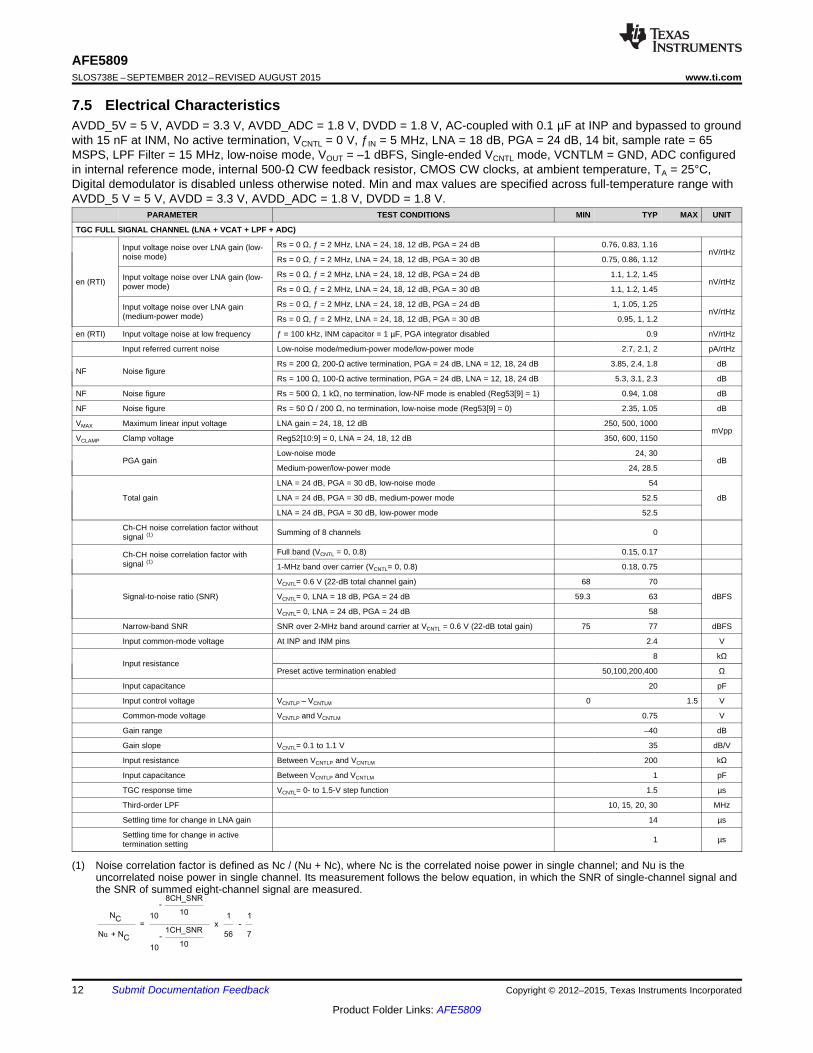
PARAMETER TEST CONDITIONS MIN TYP MAX UNIT
TGC FULL SIGNAL CHANNEL (LNA + VCAT + LPF + ADC)
Rs = 0 Ω, ƒ = 2 MHz, LNA = 24, 18, 12 dB, PGA = 24 dB 0.76, 0.83, 1.16Input voltage noise over LNA gain (low- nV/rtHznoise mode) Rs = 0 Ω, ƒ = 2 MHz, LNA = 24, 18, 12 dB, PGA = 30 dB 0.75, 0.86, 1.12
Rs = 0 Ω, ƒ = 2 MHz, LNA = 24, 18, 12 dB, PGA = 24 dB 1.1, 1.2, 1.45Input voltage noise over LNA gain (low-en (RTI) nV/rtHzpower mode) Rs = 0 Ω, ƒ = 2 MHz, LNA = 24, 18, 12 dB, PGA = 30 dB 1.1, 1.2, 1.45
Rs = 0 Ω, ƒ = 2 MHz, LNA = 24, 18, 12 dB, PGA = 24 dB 1, 1.05, 1.25Input voltage noise over LNA gain nV/rtHz(medium-power mode) Rs = 0 Ω, ƒ = 2 MHz, LNA = 24, 18, 12 dB, PGA = 30 dB 0.95, 1, 1.2
en (RTI) Input voltage noise at low frequency ƒ = 100 kHz, INM capacitor = 1 µF, PGA integrator disabled 0.9 nV/rtHz
Input referred current noise Low-noise mode/medium-power mode/low-power mode 2.7, 2.1, 2 pA/rtHz
Rs = 200 Ω, 200-Ω active termination, PGA = 24 dB, LNA = 12, 18, 24 dB 3.85, 2.4, 1.8 dBNF Noise figure
Rs = 100 Ω, 100-Ω active termination, PGA = 24 dB, LNA = 12, 18, 24 dB 5.3, 3.1, 2.3 dB
NF Noise figure Rs = 500 Ω, 1 kΩ, no termination, low-NF mode is enabled (Reg53[9] = 1) 0.94, 1.08 dB
NF Noise figure Rs = 50 Ω / 200 Ω, no termination, low-noise mode (Reg53[9] = 0) 2.35, 1.05 dB
VMAX Maximum linear input voltage LNA gain = 24, 18, 12 dB 250, 500, 1000mVpp
VCLAMP Clamp voltage Reg52[10:9] = 0, LNA = 24, 18, 12 dB 350, 600, 1150
Low-noise mode 24, 30PGA gain dB
Medium-power/low-power mode 24, 28.5
LNA = 24 dB, PGA = 30 dB, low-noise mode 54
Total gain LNA = 24 dB, PGA = 30 dB, medium-power mode 52.5 dB
LNA = 24 dB, PGA = 30 dB, low-power mode 52.5
Ch-CH noise correlation factor without Summing of 8 channels 0signal (1)
Full band (VCNTL = 0, 0.8) 0.15, 0.17Ch-CH noise correlation factor withsignal (1)
1-MHz band over carrier (VCNTL= 0, 0.8) 0.18, 0.75
VCNTL= 0.6 V (22-dB total channel gain) 68 70
Signal-to-noise ratio (SNR) VCNTL= 0, LNA = 18 dB, PGA = 24 dB 59.3 63 dBFS
VCNTL= 0, LNA = 24 dB, PGA = 24 dB 58
Narrow-band SNR SNR over 2-MHz band around carrier at VCNTL = 0.6 V (22-dB total gain) 75 77 dBFS
Input common-mode voltage At INP and INM pins 2.4 V
8 kΩInput resistance
Preset active termination enabled 50,100,200,400 Ω
Input capacitance 20 pF
Input control voltage VCNTLP – VCNTLM 0 1.5 V
Common-mode voltage VCNTLP and VCNTLM 0.75 V
Gain range –40 dB
Gain slope VCNTL= 0.1 to 1.1 V 35 dB/V
Input resistance Between VCNTLP and VCNTLM 200 kΩ
Input capacitance Between VCNTLP and VCNTLM 1 pF
TGC response time VCNTL= 0- to 1.5-V step function 1.5 µs
Third-order LPF 10, 15, 20, 30 MHz
Settling time for change in LNA gain 14 µs
Settling time for change in active 1 µstermination setting
(1) Noise correlation factor is defined as Nc / (Nu + Nc), where Nc is the correlated noise power in single channel; and Nu is theuncorrelated noise power in single channel. Its measurement follows the below equation, in which the SNR of single-channel signal andthe SNR of summed eight-channel signal are measured.
12 Submit Documentation Feedback Copyright © 2012–2015, Texas Instruments Incorporated
Product Folder Links: AFE5809

AFE5809www.ti.com SLOS738E –SEPTEMBER 2012–REVISED AUGUST 2015
Electrical Characteristics (continued)AVDD_5V = 5 V, AVDD = 3.3 V, AVDD_ADC = 1.8 V, DVDD = 1.8 V, AC-coupled with 0.1 µF at INP and bypassed to groundwith 15 nF at INM, No active termination, VCNTL = 0 V, ƒIN = 5 MHz, LNA = 18 dB, PGA = 24 dB, 14 bit, sample rate = 65MSPS, LPF Filter = 15 MHz, low-noise mode, VOUT = –1 dBFS, Single-ended VCNTL mode, VCNTLM = GND, ADC configuredin internal reference mode, internal 500-Ω CW feedback resistor, CMOS CW clocks, at ambient temperature, TA = 25°C,Digital demodulator is disabled unless otherwise noted. Min and max values are specified across full-temperature range withAVDD_5 V = 5 V, AVDD = 3.3 V, AVDD_ADC = 1.8 V, DVDD = 1.8 V.
PARAMETER TEST CONDITIONS MIN TYP MAX UNIT
AC ACCURACY
LPF bandwidth tolerance ±5%
CH-CH group delay variation 2 to 15 MHz 2 ns
CH-CH phase variation 15-MHz signal 11 °
0 V < VCNTL< 0.1 V (Dev-to-Dev) ±0.5
0.1 V < VCNTL< 1.1 V(Dev-to-Dev), TA = 25°C –1 ±0.5 1Gain matching dB
1.1 V < VCNTL< 1.5 V (Dev-to-Dev) ±0.5
0.1 V < VCNTL< 1.1 V (Dev-to-Dev), TA = 0°C and 85°C –1.1 1.1
Gain matching Channel-to-channel ±0.25 dB
Output offset VCNTL= 0, PGA = 30 dB, LNA = 24 dB –75 75 LSB
AC PERFORMANCE
FIN = 2 MHz; VOUT = –1 dBFS –60
FIN = 5 MHz; VOUT = –1 dBFS –60
FIN = 5 MHz; VIN= 500 mVPP,HD2 Second-harmonic distortion dBc–55VOUT = –1 dBFS, LNA = 18 dB, VCNTL= 0.88 V
FIN = 5 MHz; VIN = 250 mVPP,–55
VOUT = –1 dBFS, LNA = 24 dB, VCNTL= 0.88 V
FIN = 2 MHz; VOUT = –1 dBFS –55
FIN = 5 MHz; VOUT = –1 dBFS –55
FIN = 5 MHz; VIN = 500 mVPP,HD3 Third-harmonic distortion dBc–55VOUT = –1 dBFS, LNA = 18 dB, VCNTL = 0.88 V
FIN = 5 MHz; VIN = 250 mVPP,–55
VOUT = –1dBFS, LNA = 2 4dB, VCNTL= 0.88 V
FIN = 2 MHz; VOUT = –1 dBFS –55THD Total harmonic distortion dBc
FIN = 5 MHz; VOUT = – 1dBFS –55
ƒ1 = 5 MHz at –1 dBFS,IMD3 Intermodulation distortion –60 dBc
ƒ2 = 5.01 MHz at –27 dBFS
XTALK Cross-talk FIN = 5 MHz; VOUT= –1 dBFS –65 dB
Phase noise kHz off 5 MHz (VCNTL= 0 V) –132 dBc/Hz
LNA
Input referred voltage noise Rs = 0 Ω, ƒ = 2 MHz, Rin = High Z, Gain = 24, 18, 12 dB 0.63, 0.70, 0.9 nV/rtHz
50, 100, 150,High-pass filter (HPF) –3 dB cut-off frequency kHz200
LNA linear output 4 Vpp
VCAT+ PGA
VCAT input noise 0-dB, –40-dB attenuation 2, 10.5 nV/rtHz
PGA input noise 24 dB, 30 dB 1.75 nV/rtHz
–3 dB HPF cut-off frequency 80 kHz
Copyright © 2012–2015, Texas Instruments Incorporated Submit Documentation Feedback 13
Product Folder Links: AFE5809

AFE5809SLOS738E –SEPTEMBER 2012–REVISED AUGUST 2015 www.ti.com
Electrical Characteristics (continued)AVDD_5V = 5 V, AVDD = 3.3 V, AVDD_ADC = 1.8 V, DVDD = 1.8 V, AC-coupled with 0.1 µF at INP and bypassed to groundwith 15 nF at INM, No active termination, VCNTL = 0 V, ƒIN = 5 MHz, LNA = 18 dB, PGA = 24 dB, 14 bit, sample rate = 65MSPS, LPF Filter = 15 MHz, low-noise mode, VOUT = –1 dBFS, Single-ended VCNTL mode, VCNTLM = GND, ADC configuredin internal reference mode, internal 500-Ω CW feedback resistor, CMOS CW clocks, at ambient temperature, TA = 25°C,Digital demodulator is disabled unless otherwise noted. Min and max values are specified across full-temperature range withAVDD_5 V = 5 V, AVDD = 3.3 V, AVDD_ADC = 1.8 V, DVDD = 1.8 V.
PARAMETER TEST CONDITIONS MIN TYP MAX UNIT
CW DOPPLER
1-channel mixer, LNA = 24 dB, 500-Ω feedback resistor 0.8en (RTI) Input voltage noise (CW) nV/rtHz
8-channel mixer, LNA = 24 dB, 62.5-Ω feedback resistor 0.33
1-channel mixer, LNA = 24 dB, 500-Ω feedback resistor 12en (RTO) Output voltage noise (CW) nV/rtHz
8-channel mixer, LNA = 24 dB, 62.5-Ω feedback resistor 5
1-channel mixer, LNA = 18 dB, 500-Ω feedback resistor 1.1en (RTI) Input voltage noise (CW) nV/rtHz
8-channel mixer, LNA = 18 dB, 62.5-Ω feedback resistor 0.5
1-channel mixer, LNA = 18 dB, 500-Ω feedback resistor 8.1en (RTO) Output voltage noise (CW) nV/rtHz
8-channel mixer, LNA = 18 dB, 62.5-Ω feedback resistor 4
Rs = 100 Ω, RIN = High Z, FIN = 2 MHz (LNA, I/Q mixer and summingNF Noise figure 1.8 dBamplifier/filter)
fCW CW operation range (2) CW signal carrier frequency 8 MHz
1× CLK (16× mode) 8
CW clock frequency 16× CLK(16× mode) 128 MHz
4× CLK(4× mode) 32
AC coupled LVDS clock amplitude 0.7CLKM_16X-CLKP_16X; CLKM_1X-CLKP_1X Vpp
AC coupled LVPECL clock amplitude 1.6
CLK duty cycle 1× and 16× CLKs 35% 65%
Common-mode voltage Internal provided 2.5 V
VCMOS CMOS input clock amplitude 4 5 V
CW mixer conversion loss 4 dB
CW mixer phase noise 1 kHz off 2-MHz carrier 156 dBc/Hz
DR Input dynamic range FIN = 2 MHz, LNA = 24/18/12 dB 160, 164, 165 dBFS/Hz
ƒ1 = 5 MHz, ƒ2 = 5.01 MHz, both tones at –8.5-dBm amplitude, 8 channels –50 dBcsummed up in-phase, CW feedback resistor = 87 ΩIMD3 Intermodulation distortion
ƒ1 = 5 MHz, ƒ2= 5.01 MHz, both tones at –8.5-dBm amplitude, single- –60 dBcchannel case, CW feedback resistor = 500 Ω
I/Q channel gain matching 16× mode ±0.04 dB
I/Q channel phase matching 16× mode ±0.1 °
I/Q channel gain matching 4× mode ±0.04 dB
I/Q channel phase matching 4× mode ±0.1 °
Image rejection ratio FIN = 2.01 MHz, 300-mV input amplitude, CW clock frequency = 2 MHz –50 dBc
(2) In the 16× operation mode, the CW operation range is limited to 8 MHz due to the 16× CLK. The maximum clock frequency for the 16×CLK is 128 MHz. In the 8×, 4×, and 1× modes, higher CW signal frequencies up to 15 MHz can be supported with small degradation inperformance, see CW Clock Selection.
14 Submit Documentation Feedback Copyright © 2012–2015, Texas Instruments Incorporated
Product Folder Links: AFE5809

AFE5809www.ti.com SLOS738E –SEPTEMBER 2012–REVISED AUGUST 2015
Electrical Characteristics (continued)AVDD_5V = 5 V, AVDD = 3.3 V, AVDD_ADC = 1.8 V, DVDD = 1.8 V, AC-coupled with 0.1 µF at INP and bypassed to groundwith 15 nF at INM, No active termination, VCNTL = 0 V, ƒIN = 5 MHz, LNA = 18 dB, PGA = 24 dB, 14 bit, sample rate = 65MSPS, LPF Filter = 15 MHz, low-noise mode, VOUT = –1 dBFS, Single-ended VCNTL mode, VCNTLM = GND, ADC configuredin internal reference mode, internal 500-Ω CW feedback resistor, CMOS CW clocks, at ambient temperature, TA = 25°C,Digital demodulator is disabled unless otherwise noted. Min and max values are specified across full-temperature range withAVDD_5 V = 5 V, AVDD = 3.3 V, AVDD_ADC = 1.8 V, DVDD = 1.8 V.
PARAMETER TEST CONDITIONS MIN TYP MAX UNIT
CW SUMMING AMPLIFIER
VCMO Common-mode voltage Summing amplifier inputs and outputs 1.5 V
Summing amplifier output 4 Vpp
100 Hz 2 nV/rtHz
Input referred voltage noise 1 kHz 1.2 nV/rtHz
2 kHz to 100 MHz 1 nV/rtHz
Input referred current noise 2.5 pA/rtHz
Unit gain bandwidth 200 MHz
Max output current Linear operation range 20 mApp
ADC SPECIFICATIONS
Sample rate 10 65 MSPS
SNR Signal-to-noise ratio Idle channel SNR of ADC 14b 77 dBFS
REFP 1.5 VInternal reference mode
REFM 0.5 V
VREF_IN voltage 1.4 VExternal reference mode
VREF_IN current 50 µA
ADC input full-scale range 2 Vpp
LVDS rate 65 MSPS at 14 bit 910 Mbps
POWER DISSIPATION
AVDD voltage 3.15 3.3 3.6 V
AVDD_ADC voltage 1.7 1.8 1.9 V
AVDD_5V voltage 4.75 5 5.5 V
DVDD voltage 1.7 1.8 1.9 V
TGC low-noise mode, 65 MSPS 158 190
TGC low-noise mode, 40 MSPS 145Total power dissipation per channel mW/CH
TGC medium-power mode, 40 MSPS 114
TGC low-power mode, 40 MSPS 101.5
TGC low-noise mode, no signal 202 240
TGC medium-power mode, no signal 126
TGC low-power mode, no signal 99
CW-mode, no signal 147 170AVDD (3.3-V) current mA
TGC low-noise mode, 500 mVPP Input,1% duty cycle 210
TGC medium-power mode, 500 mVPP Input, 1% duty cycle 133
TGC low power, 500 mVPP Input, 1% duty cycle 105
CW-mode, 500 mVPP Input 375
TGC mode no signal 25.5 35
CW mode no signal, 16× clock = 32 MHz 32AVDD_5V current mA
TGC mode, 500-mVpp Input,1% duty cycle 26
CW-mode, 500-mVpp input 42.5
TGC low-noise mode, no signal 99 121
TGC medium-power mode, no signal 68
TGC low-power mode, no signal 55.5VCA power dissipation mW/CH
TGC low-noise mode, 500-mVPP input,1% duty cycle 102.5
TGC medium-power mode, 500-mVPP Input, 1% duty cycle 71
TGC low-power mode, 500-mVpp input,1% duty cycle 59.5
No signal, ADC shutdown CW mode no signal, 16× clock = 32 MHz 80CW power dissipation mW/CH
500-mVPP input, ADC shutdown , 16× clock = 32 MHz 173
AVDD_ADC (1.8-V) current 65MSPS 187 205 mA
DVDD (1.8-V) current 65 MSPS 77 110 mA
Copyright © 2012–2015, Texas Instruments Incorporated Submit Documentation Feedback 15
Product Folder Links: AFE5809

AFE5809SLOS738E –SEPTEMBER 2012–REVISED AUGUST 2015 www.ti.com
Electrical Characteristics (continued)AVDD_5V = 5 V, AVDD = 3.3 V, AVDD_ADC = 1.8 V, DVDD = 1.8 V, AC-coupled with 0.1 µF at INP and bypassed to groundwith 15 nF at INM, No active termination, VCNTL = 0 V, ƒIN = 5 MHz, LNA = 18 dB, PGA = 24 dB, 14 bit, sample rate = 65MSPS, LPF Filter = 15 MHz, low-noise mode, VOUT = –1 dBFS, Single-ended VCNTL mode, VCNTLM = GND, ADC configuredin internal reference mode, internal 500-Ω CW feedback resistor, CMOS CW clocks, at ambient temperature, TA = 25°C,Digital demodulator is disabled unless otherwise noted. Min and max values are specified across full-temperature range withAVDD_5 V = 5 V, AVDD = 3.3 V, AVDD_ADC = 1.8 V, DVDD = 1.8 V.
PARAMETER TEST CONDITIONS MIN TYP MAX UNIT
65 MSPS 59 69
50 MSPS 51ADC power dissipation/CH mW/CH
40 MSPS 46
20 MSPS 35
PDN_VCA = High, PDN_ADC = High 25Power dissipation in power-down mode mW/CH
Complete power-down PDN_Global = High 0.6
Power-down response time Time taken to enter power down 1 µs
2 µs + 1% ofVCA power down PDN time µsPower-up response time ADC power down 1
Complete power down 2.5 ms
FIN = 5 MHz, at 50 mVPP noise at 1 kHz on supply (3) –65 dBcPower supply modulation ratio, AVDDand AVDD_5V FIN = 5 MHz, at 50 mVpp noise at 50 kHz on supply(3) –65
ƒ = 10 kHz,VCNTL = 0 V (high gain), AVDD –40 dBc
Power supply rejection ratio ƒ = 10 kHz,VCNTL = 0 V (high gain), AVDD_5 V –55 dBc
ƒ = 10 kHz,VCNTL = 1 V (low gain), AVDD –50 dBc
(3) PSMR specification is with respect to carrier signal amplitude.
7.6 Digital Demodulator Electrical CharacteristicsAVDD_5 V = 5 V, AVDD = 3.3 V, AVDD_ADC = 1.8 V, DVDD = 1.8 V, DVDD_LDO = 1.4 V (internal generated), 14 bit/65MSPS, 4× decimation factor, at ambient temperature TA = 25°C, unless otherwise noted.
PARAMETER TEST CONDITIONS MIN TYP MAX UNITAdditional power consumption on DVDD (1.8 V) 65 MSPS, 4× decimation factor 90 mW/CHAdditional power consumption on DVDD (1.8 V) 40 MSPS, 4× decimation factor 61 mW/CH
65 MSPS, 32× decimation factor, halfAdditional power consumption on DVDD (1.8 V) 77 mW/CHLVDS pairs are powered down40 MSPS, 32× decimation factor, halfAdditional power consumption on DVDD (1.8 V) 55 mW/CHLVDS pairs are powered down
VIH Logic high input voltage, TX_SYNC pin Support 1.8-V and 3.3-V CMOS logic 1.3 3.3 VVIL Logic low input voltage, TX_SYNC pin Support 1.8-V and 3.3-V CMOS logic 0 0.3 VIIH Logic high input current, TX_SYNC pin VHIGH = 1.8 V 11 µAIIL Logic low input current, TX_SYNC pin VLOW = 0 V < 0.1 µAVIH Logic high input voltage, LDO_EN pin 1.7 3.3 VVIL Logic low input voltage, LDO_EN pin 0 0.3 VIIH Logic high input current, LDO_EN pin VHIGH = 1.8 V 11 µAIIL Logic low input current, LDO_EN pin VLOW = 0 V < 0.1 µA
16 Submit Documentation Feedback Copyright © 2012–2015, Texas Instruments Incorporated
Product Folder Links: AFE5809

AFE5809www.ti.com SLOS738E –SEPTEMBER 2012–REVISED AUGUST 2015
7.7 Digital CharacteristicsTypical values are at 25°C, AVDD = 3.3 V, AVDD_5 = 5 V and AVDD_ADC = 1.8 V, DVDD = 1.8 V unless otherwise noted.Minimum and maximum values are across the full temperature range: TMIN = 0°C to TMAX = 85°C.
PARAMETER TEST CONDITIONS MIN TYP MAX UNIT (1)
DIGITAL INPUTS/OUTPUTSVIH Logic high input voltage 2 3.3 VVIL Logic low input voltage 0 0.3 V
Logic high input current 200 µALogic low input current 200 µAInput capacitance 5 pF
VOH Logic high output voltage SDOUT pin DVDD VVOL Logic low output voltage SDOUT pin 0 VLVDS OUTPUTS
With 100-Ω external differentialOutput differential voltage 400 mVterminationOutput offset voltage Common-mode voltage 1100 mVFCLKP and FCLKM 1× clock rate 10 65 MHzDCLKP and DCLKM 7× clock rate 70 455 MHz
6× clock rate 60 390 MHztsu Data setup time (2) 350 psth Data hold time (2) 350 psADC INPUT CLOCK
Clock frequency 10 65 MSPSClock duty cycle 45% 50% 55%
Sine-wave, AC-coupled 0.5 VppClock input amplitude, LVPECL, AC-coupled 1.6 Vppdifferential(VCLKP_ADC – VCLKM_ADC)
LVDS, AC-coupled 0.7 VppCommon-mode voltage Biased internally 1 VClock input amplitude VCLKP_ADC (single- CMOS clock 1.8 Vppended)
(1) The DC specifications refer to the condition where the LVDS outputs are not switching, but are permanently at a valid logic level 0 or 1with 100-Ω external termination.
(2) Setup and hold time specifications take into account the effect of jitter on the output data and clock. These specifications also assumethat the data and clock paths are perfectly matched within the receiver. Any mismatch in these paths within the receiver would appearas reduced timing margins
Copyright © 2012–2015, Texas Instruments Incorporated Submit Documentation Feedback 17
Product Folder Links: AFE5809

AFE5809SLOS738E –SEPTEMBER 2012–REVISED AUGUST 2015 www.ti.com
7.8 Switching CharacteristicsAVDD_5 V = 5 V, AVDD = 3.3 V, AVDD_ADC = 1.8 V, DVDD = 1.8 V. Typical values are at 25°C, Differential clock, CLOAD =5 pF, RLOAD = 100 Ω, 14 bit, sample rate = 65 MSPS, digital demodulator is disabled, unless otherwise noted. Minimum andmaximum values are across the full temperature range TMIN = 0°C to TMAX = 85°C. (1)
PARAMETER TEST CONDITIONS MIN TYP MAX UNITThe delay in time between the rising edge of the input samplingta Aperture delay 0.7 3 nsclock and the actual time at which the sampling occurs.
Aperture delay Across channels within the same device ±150 psmatchingtj Aperture jitter 450 Fs rms
InputADC latency Default, after reset, or / 0 x 2 [12] = 1, LOW_LATENCY = 1 11/8 clock
cyclesData and frame clock Input clock rising edge (zero cross) to frame clock rising edge (zerotdelay 3 5.4 7 nsdelay cross) minus 3/7 of the input clock period (T)
Δtdelay Delay variation At fixed supply and 20°C T difference; device to device –1 1 nstRISE Data rise time Rise time measured from –100 to 100 mV 0.14
nsFall time measured from 100 to –100 mV 10 MHz < ƒCLKIN < 65tFALL Data fall time 0.15MHztFCLKRISE Frame clock rise time Rise time measured from –100 to 100 mV 0.14
nsFall time measured from 100 to –100 mV 10 MHz < ƒCLKIN < 65tFCLKFALL Frame clock fall time 0.15MHzFrame clock duty cycle Zero crossing of the rising edge to zero crossing of the falling edge 48% 50% 52%
tDCLKRISE Bit clock rise time Rise time measured from –100 to 100 mV 0.13nsFall time measured from 100 to –100 mV 10 MHz < ƒCLKIN < 65tDCLKFALL Bit clock fall time 0.12MHz
Zero crossing of the rising edge to zero crossing of the falling edgeBit clock duty cycle 46% 54%10 MHz < ƒCLKIN < 65 MHz
(1) Timing parameters are ensured by design and characterization; not production tested.
7.9 SPI Switching CharacteristicsMinimum values across full temperature range TMIN = 0°C to TMAX = 85°C, AVDD_5V = 5 V, AVDD = 3.3 V, AVDD_ADC = 1.8V, DVDD = 1.8 V
PARAMETER MIN TYP MAX UNITt1 SCLK period 50 nst2 SCLK high time 20 nst3 SCLK low time 20 nst4 Data setup time 5 nst5 Data hold time 5 nst6 SEN fall to SCLK rise 8 nst7 Time between last SCLK rising edge to SEN rising edge 8 nst8 SDOUT delay 12 20 28 ns
18 Submit Documentation Feedback Copyright © 2012–2015, Texas Instruments Incorporated
Product Folder Links: AFE5809

AFE5809www.ti.com SLOS738E –SEPTEMBER 2012–REVISED AUGUST 2015
7.10 Output Interface Timing Requirements (14-bit)ƒCLKIN, Setup Time (tsu), ns Hold Time (th), ns tPROG = (3/7) × T + tdelay, ns
Input ClockData Valid to Bit Clock Zero- Bit Clock Zero-Crossing to Data Input Clock Zero-Cross (Rising Edge) toFrequency (
Crossing Invalid Frame Clock Zero-Cross (Rising Edge)1)(2) (3)
MHz MIN TYP MAX MIN TYP MAX MIN TYP MAX65 0.24 0.37 0.24 0.38 11 12 12.550 0.41 0.54 0.46 0.57 13 13.9 14.440 0.55 0.70 0.61 0.73 15 16 16.730 0.87 1.10 0.94 1.1 18.5 19.5 20.120 1.30 1.56 1.46 1.6 25.7 26.7 27.3
(1) FCLK timing is the same as for the output data lines. It has the same relation to DCLK as the data pins. Setup and hold are the samefor the data and frame clock.
(2) Data valid is logic high = 100 mV and logic low = –100 mV(3) Timing parameters are ensured by design and characterization; not production tested.
SPACER
NOTEThe data from Output Interface Timing Requirements (14-bit) can be applied to 12-bit or16-bit LVDS rates as well. For example, the maximum LVDS output rate at 65 MHz and14-bit is equal to 910 MSPS, which is approximately equivalent to the rate at 56 MHz and16 bits.
Copyright © 2012–2015, Texas Instruments Incorporated Submit Documentation Feedback 19
Product Folder Links: AFE5809

14-Bit 7x Serialization Mode
LVDS Setup and Hold Timing
T0434-01
Bit Clock
DCLKP
Output Data Pair
tsu
CHi out
th
th tsu
DCLKM
Dn + 1Dn
tPROG
Frame Clock
FCLKFreq = fCLKIN
Input Clock
CLKINFreq = fCLKIN
SAMPLE N-1
D13(D0)
Data bit in MSB First mode
Data bit in LSB First mode
Bit Clock
DCLKFreq = 7 x fCLKIN
Output DataCHnOUT
Data rate = 14 x fCLKIN
D11(D0)
D10(D1)
SAMPLE N
tPROGT
Input Signal
ta
Sample NSampleN+Cd
Cd clock cycleslatency
D0
(D13)
D13
(D0)
D12
(D1)
D11
(D2)
D10
(D3)
D9
(D4)
D8
(D5)
D7
(D6)
D6
(D7)
D5
(D8)
D4
(D9)
D3
(D10)
D2
(D11)
SAMPLE N-Cd
D1(D12)
SampleN+Cd+1
D1(D12)
D0(D13)
D13
(D0)
D12
(D1)
D11
(D2)
D10
(D3)
D9
(D4)
D8
(D5)
D7
(D6)
D6
(D7)
D5
(D8)
D4
(D9)
D3
(D10)
D2
(D11)D1
(D12)D0
(D13)
D13(D0)
D12(D1)
D11
(D2)
D10
(D3)
D9
(D4)
D8
(D5)
D7
(D6)
D6
(D7)
D5
(D8)
D4
(D9)
D3
(D10)
D2
(D11)
D1
(D12)
D0(D13)
ta
12-Bit 6x Serialization Mode
AFE5809SLOS738E –SEPTEMBER 2012–REVISED AUGUST 2015 www.ti.com
Figure 1. LVDS Timing Diagrams
20 Submit Documentation Feedback Copyright © 2012–2015, Texas Instruments Incorporated
Product Folder Links: AFE5809

−0.
7
−0.
6
−0.
5
−0.
4
−0.
3
−0.
2
−0.
1 0
0.1
0.2
0.3
0.4
0.5
0.6
0.7
−0.
7
−0.
6
−0.
5
−0.
4
−0.
3
−0.
2
−0.
1 0
0.1
0.2
0.3
0.4
0.5
0.6
0.7
0
1000
2000
3000
4000
5000
6000
7000
8000
Gain (dB)
Num
ber
of O
ccur
renc
es
G005
−72
−68
−64
−60
−56
−52
−48
−44
−40
−36
−32
−28
−24
−20
−16
−12 −
8−
4 0 4 8 12 16 20 24 28 32 36 40 44 48 52 56 60 64 68
−72
−68
−64
−60
−56
−52
−48
−44
−40
−36
−32
−28
−24
−20
−16
−12 −
8−
4 0 4 8 12 16 20 24 28 32 36 40 44 48 52 56 60 64 68
0
10
20
30
40
50
60
70
80
90
100
110
120
ADC Output
Num
ber
of O
ccur
renc
es
G058
−0.
9
−0.
8
−0.
7
−0.
6
−0.
5
−0.
4
−0.
3
−0.
2
−0.
1 0
0.1
0.2
0.3
0.4
0.5
−0.
9
−0.
8
−0.
7
−0.
6
−0.
5
−0.
4
−0.
3
−0.
2
−0.
1 0
0.1
0.2
0.3
0.4
0.5
0
1000
2000
3000
4000
5000
6000
7000
8000
9000
Gain (dB)
Num
ber
of O
ccur
renc
es
G004
−0.
7
−0.
6
−0.
5
−0.
4
−0.
3
−0.
2
−0.
1 0
0.1
0.2
0.3
0.4
0.5
0.6
−0.
7
−0.
6
−0.
5
−0.
4
−0.
3
−0.
2
−0.
1 0
0.1
0.2
0.3
0.4
0.5
0.6
0
1000
2000
3000
4000
5000
6000
7000
8000
9000
Gain (dB)
Num
ber
of O
ccur
renc
es
G005
0
5
10
15
20
25
30
35
40
45
0.0 0.1 0.2 0.3 0.4 0.5 0.6 0.7 0.8 0.9 1.0 1.1 1.2 1.3 1.4 1.5Vcntl (V)
Gai
n (d
B)
Low noiseMedium powerLow power
0
5
10
15
20
25
30
35
40
45
0.0 0.1 0.2 0.3 0.4 0.5 0.6 0.7 0.8 0.9 1.0 1.1 1.2Vcntl (V)
Gai
n (d
B)
−40 deg C25 deg C85 deg C
AFE5809www.ti.com SLOS738E –SEPTEMBER 2012–REVISED AUGUST 2015
7.11 Typical CharacteristicsAVDD_5 V = 5 V, AVDD = 3.3 V, AVDD_ADC = 1.8 V, DVDD = 1.8 V, AC-coupled with 0.1-µF capacitors at INP and 15-nFcapacitors at INM, No active termination, VCNTL = 0 V, FIN = 5 MHz, LNA = 18 dB, PGA = 24 dB, 14 bit, sample rate = 65MSPS, LPF filter = 15 MHz, low-noise mode, Single-ended VCNTL mode, VCNTLM = GND, ADC is configured in internalreference mode, VOUT = –1 dBFS, 500-Ω CW feedback resistor, CMOS 16× clock, digital demodulator is disabled, at ambienttemperature TA = 25°C, unless otherwise noted.
Figure 2. Gain vs VCNTL, LNA = 18 dB and PGA = 24 dB Figure 3. Gain Variation vs Temperature, LNA = 18 dB andPGA = 24 dB
Figure 4. Gain Matching Histogram, VCNTL = 0.3 V (34951 Figure 5. Gain Matching Histogram, VCNTL = 0.6 V (34951Channels) Channels)
Figure 6. Gain Matching Histogram, VCNTL = 0.9 V (34951 Figure 7. Output Offset Histogram, VCNTL = 0 V (1247Channels) Channels)
Copyright © 2012–2015, Texas Instruments Incorporated Submit Documentation Feedback 21
Product Folder Links: AFE5809

−30
−27
−24
−21
−18
−15
−12
−9
−6
−3
0
3
10 100 500
Frequency (kHz)
Am
plit
ude (
dB
)
01
00
11
10−30
−25
−20
−15
−10
−5
0
5
0 10 20 30 40 50 60
Frequency (MHz)
Am
plitu
de (
dB)
10MHz15MHz20MHz30MHz
0
50
100
150
200
250
300
350
400
450
500
500k 4.5M 8.5M 12.5M 16.5M 20.5M
Frequency (Hz)
Imp
ed
an
ce
()
Ω
50 Ω
100 Ω
200 Ω
400 Ω
−90
−80
−70
−60
−50
−40
−30
−20
−10
0
10
500k 4.5M 8.5M 12.5M 16.5M 20.5M
Frequency (Hz)
Ph
ase
(D
eg
ree
s)
50 Ω
100 Ω
200 Ω
400 Ω
−90
−80
−70
−60
−50
−40
−30
−20
−10
0
10
500k 4.5M 8.5M 12.5M 16.5M 20.5M
Frequency (Hz)
Ph
ase
(D
eg
ree
s)
Open
2000
4000
6000
8000
10000
12000
500k 4.5M 8.5M 12.5M 16.5M 20.5M
Frequency (Hz)
Imp
ed
an
ce
()
Ω
Open
AFE5809SLOS738E –SEPTEMBER 2012–REVISED AUGUST 2015 www.ti.com
Typical Characteristics (continued)AVDD_5 V = 5 V, AVDD = 3.3 V, AVDD_ADC = 1.8 V, DVDD = 1.8 V, AC-coupled with 0.1-µF capacitors at INP and 15-nFcapacitors at INM, No active termination, VCNTL = 0 V, FIN = 5 MHz, LNA = 18 dB, PGA = 24 dB, 14 bit, sample rate = 65MSPS, LPF filter = 15 MHz, low-noise mode, Single-ended VCNTL mode, VCNTLM = GND, ADC is configured in internalreference mode, VOUT = –1 dBFS, 500-Ω CW feedback resistor, CMOS 16× clock, digital demodulator is disabled, at ambienttemperature TA = 25°C, unless otherwise noted.
Figure 8. Input Impedance Without Active Termination Figure 9. Input Impedance Without Active Termination(Magnitude) (Phase)
Figure 10. Input Impedance With Active Termination Figure 11. Input Impedance With Active Termination (Phase)(Magnitude)
Figure 12. LPF Response Figure 13. LNA HPF Response vs Reg59[3:2]
22 Submit Documentation Feedback Copyright © 2012–2015, Texas Instruments Incorporated
Product Folder Links: AFE5809

0
10
20
30
40
50
60
0.0 0.1 0.2 0.3 0.4 0.5 0.6 0.7 0.8 0.9 1.0 1.1 1.2Vcntl (V)
Inpu
t ref
fere
d no
ise
(nV
Hz
)
LNA 12 dBLNA 18 dBLNA 24 dB
0.0
0.5
1.0
1.5
2.0
2.5
3.0
3.5
0.0 0.1 0.2 0.3 0.4Vcntl (V)
Inpu
t ref
fere
d no
ise
(nV
Hz
)
LNA 12 dBLNA 18 dBLNA 24 dB
−170
−168
−166
−164
−162
−160
−158
−156
−154
−152
−150
−148
−146
100 1000 10000 50000
Frequency Offset (Hz)
Phase N
ois
e (
dB
c/H
z)
PN 1 Ch
PN 8 Ch
−170
−168
−166
−164
−162
−160
−158
−156
−154
−152
−150
−148
−146
100 1000 10000 50000
Offset Frequency (Hz)
Phase N
ois
e (
dB
c/H
z)
16X Clock Mode
8X Clock Mode
4X Clock Mode
−40
−35
−30
−25
−20
−15
−10
−5
0
5
10 100 500
Frequency (kHz)
Am
plit
ude (
dB
)
−170
−168
−166
−164
−162
−160
−158
−156
−154
−152
−150
−148
−146
100 1000 10000 50000
Offset Frequency (Hz)
Pha
se
No
ise
(d
Bc/H
z)
16X Clock Mode
8X Clock Mode
4X Clock Mode
AFE5809www.ti.com SLOS738E –SEPTEMBER 2012–REVISED AUGUST 2015
Typical Characteristics (continued)AVDD_5 V = 5 V, AVDD = 3.3 V, AVDD_ADC = 1.8 V, DVDD = 1.8 V, AC-coupled with 0.1-µF capacitors at INP and 15-nFcapacitors at INM, No active termination, VCNTL = 0 V, FIN = 5 MHz, LNA = 18 dB, PGA = 24 dB, 14 bit, sample rate = 65MSPS, LPF filter = 15 MHz, low-noise mode, Single-ended VCNTL mode, VCNTLM = GND, ADC is configured in internalreference mode, VOUT = –1 dBFS, 500-Ω CW feedback resistor, CMOS 16× clock, digital demodulator is disabled, at ambienttemperature TA = 25°C, unless otherwise noted.
Figure 15. CW Phase Noise, FIN = 2 MHzFigure 14. Full Channel HPF Response at Default RegisterSetting
Figure 16. CW Phase Noise, FIN = 2 MHz, 1 Channel vs 8 Figure 17. CW Phase Noise vs Clock Modes, FIN= 2 MHzChannel
Figure 18. IRN, PGA = 24 dB and Low Noise Mode Figure 19. IRN, PGA = 24 dB and Low Noise Mode
Copyright © 2012–2015, Texas Instruments Incorporated Submit Documentation Feedback 23
Product Folder Links: AFE5809

30
50
70
90
110
130
150
170
190
210220
0.0 0.1 0.2 0.3 0.4 0.5 0.6 0.7 0.8 0.9 1.0 1.1 1.2Vcntl (V)
Out
put r
effe
red
nois
e (n
VH
z)
LNA 12 dBLNA 18 dBLNA 24 dB
40
60
80
100
120
140
160
180
200
220
240
260
280
300
0.0 0.1 0.2 0.3 0.4 0.5 0.6 0.7 0.8 0.9 1.0 1.1 1.2Vcntl (V)
Out
put r
effe
red
nois
e (n
VH
z)
LNA 12 dBLNA 18 dBLNA 24 dB
0
10
20
30
40
50
60
70
0.0 0.1 0.2 0.3 0.4 0.5 0.6 0.7 0.8 0.9 1.0 1.1 1.2Vcntl (V)
Inpu
t ref
fere
d no
ise
(nV
Hz
)
LNA 12 dBLNA 18 dBLNA 24 dB
0.5
1.0
1.5
2.0
2.5
3.0
3.5
4.0
0.0 0.1 0.2 0.3 0.4Vcntl (V)
Inpu
t ref
fere
d no
ise
(nV
Hz
)LNA 12 dBLNA 18 dBLNA 24 dB
0
10
20
30
40
50
60
70
0.0 0.1 0.2 0.3 0.4 0.5 0.6 0.7 0.8 0.9 1.0 1.1 1.2Vcntl (V)
Inpu
t ref
fere
d no
ise
(nV
Hz
)
LNA 12 dBLNA 18 dBLNA 24 dB
0.5
1.0
1.5
2.0
2.5
3.0
3.5
4.0
0.0 0.1 0.2 0.3 0.4Vcntl (V)
Inpu
t ref
fere
d no
ise
(nV
Hz
)
LNA 12 dBLNA 18 dBLNA 24 dB
AFE5809SLOS738E –SEPTEMBER 2012–REVISED AUGUST 2015 www.ti.com
Typical Characteristics (continued)AVDD_5 V = 5 V, AVDD = 3.3 V, AVDD_ADC = 1.8 V, DVDD = 1.8 V, AC-coupled with 0.1-µF capacitors at INP and 15-nFcapacitors at INM, No active termination, VCNTL = 0 V, FIN = 5 MHz, LNA = 18 dB, PGA = 24 dB, 14 bit, sample rate = 65MSPS, LPF filter = 15 MHz, low-noise mode, Single-ended VCNTL mode, VCNTLM = GND, ADC is configured in internalreference mode, VOUT = –1 dBFS, 500-Ω CW feedback resistor, CMOS 16× clock, digital demodulator is disabled, at ambienttemperature TA = 25°C, unless otherwise noted.
Figure 20. IRN, PGA = 24 dB and Medium-Power Mode Figure 21. IRN, PGA = 24 dB and Medium-Power Mode
Figure 22. IRN, PGA = 24 dB and Low-Power Mode Figure 23. IRN, PGA = 24 dB and Low-Power Mode
Figure 24. ORN, PGA = 24 dB and Low Noise Mode Figure 25. ORN, PGA = 24 dB and Medium-Power Mode
24 Submit Documentation Feedback Copyright © 2012–2015, Texas Instruments Incorporated
Product Folder Links: AFE5809
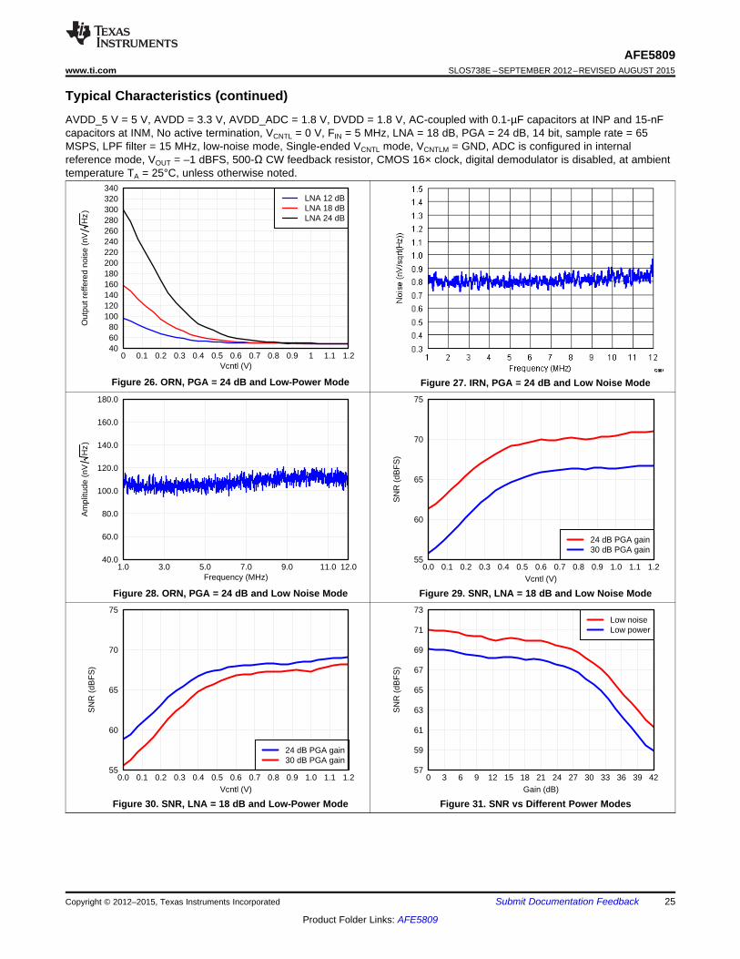
55
60
65
70
75
0.0 0.1 0.2 0.3 0.4 0.5 0.6 0.7 0.8 0.9 1.0 1.1 1.2Vcntl (V)
SN
R (
dBF
S)
24 dB PGA gain30 dB PGA gain
57
59
61
63
65
67
69
71
73
0 3 6 9 12 15 18 21 24 27 30 33 36 39 42Gain (dB)
SN
R (
dBF
S)
Low noiseLow power
40.0
60.0
80.0
100.0
120.0
140.0
160.0
180.0
1.0 3.0 5.0 7.0 9.0 11.0 12.0Frequency (MHz)
Am
plitu
de (
nVH
z)
55
60
65
70
75
0.0 0.1 0.2 0.3 0.4 0.5 0.6 0.7 0.8 0.9 1.0 1.1 1.2Vcntl (V)
SN
R (
dBF
S)
24 dB PGA gain30 dB PGA gain
406080
100120140160180200220240260280300320340
0 0.1 0.2 0.3 0.4 0.5 0.6 0.7 0.8 0.9 1 1.1 1.2Vcntl (V)
Out
put r
effe
red
nois
e (n
VH
z)
LNA 12 dBLNA 18 dBLNA 24 dB
AFE5809www.ti.com SLOS738E –SEPTEMBER 2012–REVISED AUGUST 2015
Typical Characteristics (continued)AVDD_5 V = 5 V, AVDD = 3.3 V, AVDD_ADC = 1.8 V, DVDD = 1.8 V, AC-coupled with 0.1-µF capacitors at INP and 15-nFcapacitors at INM, No active termination, VCNTL = 0 V, FIN = 5 MHz, LNA = 18 dB, PGA = 24 dB, 14 bit, sample rate = 65MSPS, LPF filter = 15 MHz, low-noise mode, Single-ended VCNTL mode, VCNTLM = GND, ADC is configured in internalreference mode, VOUT = –1 dBFS, 500-Ω CW feedback resistor, CMOS 16× clock, digital demodulator is disabled, at ambienttemperature TA = 25°C, unless otherwise noted.
Figure 26. ORN, PGA = 24 dB and Low-Power Mode Figure 27. IRN, PGA = 24 dB and Low Noise Mode
Figure 28. ORN, PGA = 24 dB and Low Noise Mode Figure 29. SNR, LNA = 18 dB and Low Noise Mode
Figure 30. SNR, LNA = 18 dB and Low-Power Mode Figure 31. SNR vs Different Power Modes
Copyright © 2012–2015, Texas Instruments Incorporated Submit Documentation Feedback 25
Product Folder Links: AFE5809

−80.0
−75.0
−70.0
−65.0
−60.0
−55.0
−50.0
1 2 3 4 5 6 7 8 9 10Frequency (MHz)
HD
2 (d
B)
Low noiseLow powerMedium power
0
1
2
3
4
5
6
7
8
50 100 150 200 250 300 350 400
Source Impedence (Ω)
Noi
se F
igur
e (d
B)
50 ohm act term100 ohm act term200 ohm act term400 ohm act termNo Termination
0
1
2
3
4
5
6
7
8
9
50 100 150 200 250 300 350 400
Source Impedence (Ω)
Noi
se F
igur
e (d
B)
100 ohm act term200 ohm act term400 ohm act termWithout Termination
0
1
2
3
4
5
6
7
8
9
10
50 100 150 200 250 300 350 400
Source Impedence (Ω)
Noi
se F
igur
e (d
B)
50 ohm act term100 ohm act term200 ohm act term400 ohm act termWithout Termination
AFE5809SLOS738E –SEPTEMBER 2012–REVISED AUGUST 2015 www.ti.com
Typical Characteristics (continued)AVDD_5 V = 5 V, AVDD = 3.3 V, AVDD_ADC = 1.8 V, DVDD = 1.8 V, AC-coupled with 0.1-µF capacitors at INP and 15-nFcapacitors at INM, No active termination, VCNTL = 0 V, FIN = 5 MHz, LNA = 18 dB, PGA = 24 dB, 14 bit, sample rate = 65MSPS, LPF filter = 15 MHz, low-noise mode, Single-ended VCNTL mode, VCNTLM = GND, ADC is configured in internalreference mode, VOUT = –1 dBFS, 500-Ω CW feedback resistor, CMOS 16× clock, digital demodulator is disabled, at ambienttemperature TA = 25°C, unless otherwise noted.
Figure 32. Noise Figure, LNA = 12 dB and Low Noise Mode Figure 33. Noise Figure, LNA = 18 dB and Low Noise Mode
Figure 34. Noise Figure, LNA = 24 dB and Low Noise Mode Figure 35. Noise Figure vs Power Modes With 400-ΩTermination
Figure 37. HD2 vs Frequency, VIN = 500 mVpp andFigure 36. Noise Figure vs Power Modes WithoutVOUT = –1 dBFSTermination
26 Submit Documentation Feedback Copyright © 2012–2015, Texas Instruments Incorporated
Product Folder Links: AFE5809

−90
−80
−70
−60
−50
−40
12 18 24 30 36 42Gain (dB)
HD
3 (d
Bc)
Low noiseLow powerMedium power
−90
−85
−80
−75
−70
−65
−60
−55
−50
−45
−40
18 24 30 36 42 48Gain (dB)
HD
2 (d
Bc)
Low noiseLow powerMedium power
−90
−80
−70
−60
−50
−40
6 12 18 24 30 36Gain (dB)
HD
3 (d
Bc)
Low noiseLow powerMedium power
−90
−80
−70
−60
−50
−40
12 18 24 30 36 42Gain (dB)
HD
2 (d
Bc)
Low noiseLow powerMedium power
−75
−70
−65
−60
−55
−50
−45
1 2 3 4 5 6 7 8 9 10Frequency (MHz)
HD
3 (d
Bc)
Low noiseLow powerMedium power
−90
−85
−80
−75
−70
−65
−60
−55
−50
−45
−40
6 12 18 24 30 36Gain (dB)
HD
2 (d
Bc)
Low noiseLow powerMedium power
AFE5809www.ti.com SLOS738E –SEPTEMBER 2012–REVISED AUGUST 2015
Typical Characteristics (continued)AVDD_5 V = 5 V, AVDD = 3.3 V, AVDD_ADC = 1.8 V, DVDD = 1.8 V, AC-coupled with 0.1-µF capacitors at INP and 15-nFcapacitors at INM, No active termination, VCNTL = 0 V, FIN = 5 MHz, LNA = 18 dB, PGA = 24 dB, 14 bit, sample rate = 65MSPS, LPF filter = 15 MHz, low-noise mode, Single-ended VCNTL mode, VCNTLM = GND, ADC is configured in internalreference mode, VOUT = –1 dBFS, 500-Ω CW feedback resistor, CMOS 16× clock, digital demodulator is disabled, at ambienttemperature TA = 25°C, unless otherwise noted.
Figure 38. HD3 vs Frequency, VIN = 500 mVpp and Figure 39. HD2 vs Gain, LNA = 12 dB and PGA = 24 dB andVOUT = –1 dBFSVOUT = –1 dBFS
Figure 40. HD3 vs Gain, LNA = 12 dB and PGA = 24 dB and Figure 41. HD2 vs Gain, LNA = 18 dB and PGA = 24 dB andVOUT = –1 dBFS VOUT = –1 dBFS
Figure 42. HD3 vs Gain, LNA = 18 dB and PGA = 24 dB and Figure 43. HD2 vs Gain, LNA = 24 dB and PGA = 24 dB andVOUT = –1 dBFS VOUT = –1 dBFS
Copyright © 2012–2015, Texas Instruments Incorporated Submit Documentation Feedback 27
Product Folder Links: AFE5809

−80
−75
−70
−65
−60
−55
5 10 100 1000 2000
Supply Frequency (kHz)
PS
MR
(dB
c)
Vcntl = 0
Vcntl = 0.3
Vcntl = 0.6
Vcntl = 0.9
−90
−80
−70
−60
−50
−40
−30
−20
5 10 100 1000 2000
Supply Frequency (kHz)
PS
RR
wrt
supply
tone (
dB
)
Vcntl = 0
Vcntl = 0.3
Vcntl = 0.6
Vcntl = 0.9
−75
−70
−65
−60
5 10 100 1000 2000
Supply Frequency (kHz)
PS
MR
(d
Bc)
Vcntl = 0
Vcntl = 0.3
Vcntl = 0.6
Vcntl = 0.9
−70
−66
−62
−58
−54
−50
14 18 22 26 30 34 38 42Gain (dB)
IMD
3 (d
BF
S)
Fin1=2MHz, Fin2=2.01MHzFin1=5MHz, Fin2=5.01MHz
G001
−90
−80
−70
−60
−50
−40
18 21 24 27 30 33 36 39 42 45 48Gain (dB)
HD
3 (d
B)
Low noiseLow powerMedium power
−70
−66
−62
−58
−54
−50
14 18 22 26 30 34 38 42Gain (dB)
IMD
3 (d
BF
S)
Fin1=2MHz, Fin2=2.01MHzFin1=5MHz, Fin2=5.01MHz
G001
AFE5809SLOS738E –SEPTEMBER 2012–REVISED AUGUST 2015 www.ti.com
Typical Characteristics (continued)AVDD_5 V = 5 V, AVDD = 3.3 V, AVDD_ADC = 1.8 V, DVDD = 1.8 V, AC-coupled with 0.1-µF capacitors at INP and 15-nFcapacitors at INM, No active termination, VCNTL = 0 V, FIN = 5 MHz, LNA = 18 dB, PGA = 24 dB, 14 bit, sample rate = 65MSPS, LPF filter = 15 MHz, low-noise mode, Single-ended VCNTL mode, VCNTLM = GND, ADC is configured in internalreference mode, VOUT = –1 dBFS, 500-Ω CW feedback resistor, CMOS 16× clock, digital demodulator is disabled, at ambienttemperature TA = 25°C, unless otherwise noted.
Figure 45. IMD3, Fout1 = –7 dBFS and Fout2 = –21 dBFSFigure 44. HD3 vs Gain, LNA = 24 dB and PGA = 24 dB andVOUT = –1 dBFS
Figure 46. IMD3, Fout1 = –7 dBFS and Fout2 = –7 dBFS Figure 47. AVDD Power Supply Modulation Ratio, 100 mVppSupply Noise With Different Frequencies
Figure 48. AVDD_5V Power Supply Modulation Ratio, Figure 49. AVDD Power Supply Rejection Ratio, 100 mVppSupply Noise With Different Frequencies100 mVpp Supply Noise With Different Frequencies
28 Submit Documentation Feedback Copyright © 2012–2015, Texas Instruments Incorporated
Product Folder Links: AFE5809

−1.2
−1.0
−0.8
−0.6
−0.4
−0.2
0.0
0.2
0.4
0.6
0.8
1.0
1.2
0.0 2.0 4.0 6.0 8.0 10.0 12.0 14.0 16.0 18.0 20.0Time (µs)
Inpu
t (V
)
−10000.0
−8000.0
−6000.0
−4000.0
−2000.0
0.0
2000.0
4000.0
6000.0
8000.0
10000.0
0.0 1.0 2.0 3.0 4.0 5.0 6.0Time (µs)
Out
put C
ode
Positive overloadNegative overloadAverage
−1.2
−1.0
−0.8
−0.6
−0.4
−0.2
0.0
0.2
0.4
0.6
0.8
1.0
1.2
0.0 2.0 4.0 6.0 8.0 10.0 12.0 14.0 16.0 18.0 20.0Time (µs)
Inpu
t (V
)
0.0 0.2 0.5 0.8 1.0 1.2 1.5 1.8 2.0 2.2 2.50.0
2000.0
4000.0
6000.0
8000.0
10000.0
12000.0
14000.0
16000.0
18000.0
20000.0
−0.10.00.10.20.30.40.50.60.70.80.91.01.11.21.3
Time (µs)
Out
put C
ode
Vcn
tl (V
)
Output CodeVcntl
−90
−80
−70
−60
−50
−40
−30
−20
5 10 100 1000 2000
Supply Frequency (kHz)
PS
RR
With R
espect to
Supply
Tone (
dB
) Vcntl = 0
Vcntl = 0.3
Vcntl = 0.6
Vcntl = 0.9
0.0 0.5 1.0 1.5 2.0 2.5 3.00.0
2000.0
4000.0
6000.0
8000.0
10000.0
12000.0
14000.0
16000.0
18000.0
20000.0
−0.10.00.10.20.30.40.50.60.70.80.91.01.11.21.3
Time (µs)
Out
put C
ode
Vcn
tl (V
)
Output CodeVcntl
AFE5809www.ti.com SLOS738E –SEPTEMBER 2012–REVISED AUGUST 2015
Typical Characteristics (continued)AVDD_5 V = 5 V, AVDD = 3.3 V, AVDD_ADC = 1.8 V, DVDD = 1.8 V, AC-coupled with 0.1-µF capacitors at INP and 15-nFcapacitors at INM, No active termination, VCNTL = 0 V, FIN = 5 MHz, LNA = 18 dB, PGA = 24 dB, 14 bit, sample rate = 65MSPS, LPF filter = 15 MHz, low-noise mode, Single-ended VCNTL mode, VCNTLM = GND, ADC is configured in internalreference mode, VOUT = –1 dBFS, 500-Ω CW feedback resistor, CMOS 16× clock, digital demodulator is disabled, at ambienttemperature TA = 25°C, unless otherwise noted.
Figure 50. AVDD_5V Power Supply Rejection Ratio, Figure 51. VCNTL Response Time, LNA = 18 dB and100 mVpp Supply Noise With Different Frequencies PGA = 24 dB
Figure 52. VCNTL Response Time, LNA = 18 dB andFigure 53. Pulse Inversion Asymmetrical Positive InputPGA = 24 dB
Figure 54. Pulse Inversion Asymmetrical Negative Input Figure 55. Pulse Inversion, VIN = 2 Vpp, PRF = 1 kHz,Gain = 21 dB
Copyright © 2012–2015, Texas Instruments Incorporated Submit Documentation Feedback 29
Product Folder Links: AFE5809

−40
−35
−30
−25
−20
−15
−10
−5
0
5
10
0 0.2 0.4 0.6 0.8 1 1.2 1.4 1.6 1.8 2Frequency (MHz)
Gai
n (d
B) k=2
k=3k=4k=5k=6k=7k=8k=9k=10
G000
−10000
−8000
−6000
−4000
−2000
0
2000
4000
6000
8000
10000
0 0.5 1 1.5 2 2.5 3 3.5 4 4.5 5Time (µs)
Out
put C
ode
47nF15nF
−2000
−1600
−1200
−800
−400
0
400
800
1200
1600
2000
1 1.5 2 2.5 3 3.5 4 4.5 5Time (µs)
Out
put C
ode
47nF15nF
AFE5809SLOS738E –SEPTEMBER 2012–REVISED AUGUST 2015 www.ti.com
Typical Characteristics (continued)AVDD_5 V = 5 V, AVDD = 3.3 V, AVDD_ADC = 1.8 V, DVDD = 1.8 V, AC-coupled with 0.1-µF capacitors at INP and 15-nFcapacitors at INM, No active termination, VCNTL = 0 V, FIN = 5 MHz, LNA = 18 dB, PGA = 24 dB, 14 bit, sample rate = 65MSPS, LPF filter = 15 MHz, low-noise mode, Single-ended VCNTL mode, VCNTLM = GND, ADC is configured in internalreference mode, VOUT = –1 dBFS, 500-Ω CW feedback resistor, CMOS 16× clock, digital demodulator is disabled, at ambienttemperature TA = 25°C, unless otherwise noted.
Figure 56. Overload Recovery Response vs INM Capacitor, Figure 57. Overload Recovery Response vs INM CapacitorVIN = 50 mVpp/100 µVpp, Max Gain (Zoomed), VIN = 50 mVpp/100 µVpp, Max Gain
Figure 59. Signal Chain Low Frequency Response With INMFigure 58. Digital HPF ResponseCapacitor = 1 µF
30 Submit Documentation Feedback Copyright © 2012–2015, Texas Instruments Incorporated
Product Folder Links: AFE5809

SPI
LNAVCAT0 to -40 dB
SPI Logic
16X CLKP
INPGA
24, 30dB
3rd
LP Filter10, 15, 20, 30
MHz
16 Phases
GeneratorCW Mixer Summing
Amplifier/ Filter16X CLKN
1X CLK
CW I/Q Vout
AFE5809 with Demodulator1 of 8 Channels
14 Bit
ADCLVDS
OUT
ReferenceReference
DifferentialTGC Vcntl
EXT/INTREFM/P
DigitalDeMod &LP Filter
LVDSSerializer
Logic
Control
DeModControl
AFE5809www.ti.com SLOS738E –SEPTEMBER 2012–REVISED AUGUST 2015
8 Detailed Description
8.1 OverviewThe AFE5809 device is a highly-integrated AFE solution specifically designed for ultrasound systems in whichhigh performance and small size are required. The AFE5809 device integrates a complete TGC imaging pathand a CWD path. It also enables users to select one of various power/noise combinations to optimize systemperformance. The AFE5809 device contains eight channels; each channel includes a LNA, VCAT, PGA, LPF, 14-bit ADC, digital I/Q demodulator, and CW mixer.
Multiple features in the AFE5809 device are suitable for ultrasound applications, such as active termination,individual channel control, fast power-up and power-down response, programmable clamp voltage control, andfast and consistent overload recovery. Therefore, the AFE5809 device brings premium image quality toultraportable, handheld systems all the way up to high-end ultrasound systems.
In addition, the signal chain of the AFE5809 device can handle signal frequency as low as 50 kHz and as high as30 MHz. This enables the AFE5809 device to be used in both sonar and medical applications.
Figure 60 shows a simplified functional block diagram.
8.2 Functional Block Diagram
Figure 60. Simplified Functional Block Diagram
Copyright © 2012–2015, Texas Instruments Incorporated Submit Documentation Feedback 31
Product Folder Links: AFE5809

DCRemoval
DownConversion
SamplesRAM
DecimationFilter
DCRemoval
DownConversion
DecimationFilter
Serializer
COS -SIN
COS -SIN
ADC 1
ADC 2
LVDS 1
LVDS 2
LVDS 3
LVDS 4
640Mbps
ADC 3
14bit 40MHz
ADC 4
14bit 40MHz
ADC 5
14bit 40MHz
ADC 6
14bit 40MHz
ADC 7
14bit 40MHz
ADC 8
14bit 40MHz
Channels 1, 2
Channels 3, 4
Channels 5, 6
Channels 7, 8
COS & -SIN
Table
CoefficientMemory
Regsiters Control
COS -SIN
Freq
C0 Cn. . .
14bit
40MHz
14bit
40MHz
C0 Cn. . .
C0 Cn. . .
Control
I
Q
I
Q
I
Q
I
Q
I
Q
I
Q
640Mbps
640Mbps
640Mbps
AFE5809SLOS738E –SEPTEMBER 2012–REVISED AUGUST 2015 www.ti.com
Functional Block Diagram (continued)
Figure 61. Digital Demodulator Block Diagram
8.3 Feature Description
8.3.1 LNAIn many high-gain systems, a LNA is critical to achieve overall performance. Using a new proprietaryarchitecture, the LNA in the AFE5809 device delivers exceptional low-noise performance, while operating on alow-quiescent current compared to CMOS-based architectures with similar noise performance. The LNAperforms single-ended input to differential output voltage conversion. It is configurable for a programmable gainof 24, 18, or 12 dB and its input-referred noise is only 0.63, 0.7, or 0.9 nV/√Hz, respectively. Programmable gainsettings result in a flexible linear input range up to 1 Vpp, realizing high-signal handling capability demanded bynew transducer technologies. A larger input signal can be accepted by the LNA; however, the signal can bedistorted because it exceeds the LNA’s linear operation region. Combining the low noise and high-input range,the device consequently achieves a wide-input dynamic range for supporting the high demands from variousultrasound imaging modes.
32 Submit Documentation Feedback Copyright © 2012–2015, Texas Instruments Incorporated
Product Folder Links: AFE5809

LNAx
INPx
INMx
ACTx
INPUT
AFE
CACT
CIN
CBYPSS
CLAMP
DC Offset
Correction
AFE5809www.ti.com SLOS738E –SEPTEMBER 2012–REVISED AUGUST 2015
Feature Description (continued)The LNA input is internally biased at approximately 2.4 V; the signal source should be AC-coupled to the LNAinput by an adequately-sized capacitor, for example ≥0.1 µF. To achieve low DC offset drift, the AFE5809 deviceincorporates a DC offset correction circuit for each amplifier stage. To improve the overload recovery, anintegrator circuit is used to extract the DC component of the LNA output and then fed back to the LNA’scomplementary input for DC offset correction. This DC offset correction circuit has a high-pass response and canbe treated as a HPF. The effective corner frequency is determined by the capacitor CBYPASS connected at INM.With larger capacitors, the corner frequency is lower. For stable operation at the highest HP filter cut-offfrequency, a ≥15-nF capacitor can be selected. This corner frequency scales almost linearly with the value of theCBYPASS. For example, 15 nF gives a corner frequency of approximately 100 kHz, while 47 nF can give aneffective corner frequency of 33 kHz. The DC offset correction circuit can also be disabled or enabled throughregister 52[12]. A large capacitor like 1 µF can be used for setting low corner frequency (<2 kHz) of the LNA DCoffset correction circuit. Figure 59 shows the frequency responses for low-frequency applications.
The AFE5809 device can be terminated passively or actively. Active termination is preferred in ultrasoundapplications for reducing reflection from mismatches and achieving better axial resolution without degradingnoise figure too much. Active termination values can be preset to 50, 100, 200, and 400 Ω; other values also canbe programmed by users through register 52[4:0]. A feedback capacitor is required between ACTx and the signalsource as Figure 62 shows. On the active termination path, a clamping circuit is also used to create a low-impedance path when overload signal is seen by the AFE5809 device. The clamp circuit limits large input signalsat the LNA inputs and improves the overload recovery performance of the AFE5809 device. The clamp level canbe set to 350 mVpp, 600 mVpp, or 1.15 Vpp automatically depending on the LNA gain settings when register52[10:9] = 0. Other clamp voltages, such as 1.15 Vpp, 0.6 Vpp, and 1.5 Vpp, are also achievable by settingregister 52[10:9]. This clamping circuit is also designed to obtain good pulse inversion performance and reducethe impact from asymmetric inputs.
Figure 62. AFE5809 LNA With DC Offset Correction Circuit
8.3.2 Voltage-Controlled AttenuatorThe voltage-controlled attenuator is designed to have a linear-in-dB attenuation characteristic; that is, theaverage gain loss in dB (refer to Figure 2) is constant for each equal increment of the control voltage (VCNTL) asshown in Figure 63. A differential control structure is used to reduce common mode noise. Figure 63 andFigure 64 show a simplified attenuator structure.
The attenuator is essentially a variable voltage divider that consists of the series input resistor (RS) and sevenshunt FETs placed in parallel and controlled by sequentially activated clipping amplifiers (A1 through A7). VCNTLis the effective difference between VCNTLP and VCNTLM. Each clipping amplifier can be understood as aspecialized voltage comparator with a soft transfer characteristic and well-controlled output limit voltage.Reference voltages V1 through V7 are equally spaced over the 0- to 1.5-V control voltage range. As the controlvoltage increases through the input range of each clipping amplifier, the amplifier output rises from a voltagewhere the FET is nearly OFF to VHIGH where the FET is completely ON. As each FET approaches its ON state
Copyright © 2012–2015, Texas Instruments Incorporated Submit Documentation Feedback 33
Product Folder Links: AFE5809

RS
Q1
VB
Q2 Q3 Q4 Q5 Q6 Q7
VHIGH
AttenuatorOutput
AttenuatorInput
SW1 SW2 SW3 SW4 SW5 SW6 SW7
RS
Control
Input
Q1
VB
Q2 Q3
C1
V1
Q4 Q5 Q6 Q7
C2
V2
C3
V3
C4
V4
C5
V5
C6
V6
C7
V7
A1
VCNTL
A1 A1 A1 A1 A1 A1
AttenuatorOutput
C - C Clipping Amplifiers1 8
A1 - A7 Attenuator Stages
AttenuatorInput
AFE5809SLOS738E –SEPTEMBER 2012–REVISED AUGUST 2015 www.ti.com
Feature Description (continued)and the control voltage continues to rise, the next clipping amplifier/FET combination takes over for the nextportion of the piecewise-linear attenuation characteristic. Thus, low control voltages have most of the FETsturned OFF, producing minimum signal attenuation. Similarly, high control voltages turn the FETs ON, leading tomaximum signal attenuation. Therefore, each FET acts to decrease the shunt resistance of the voltage dividerformed by RS and the parallel FET network.
Additionally, a digitally-controlled TGC mode is implemented to achieve better phase-noise performance in theAFE5809 device. The attenuator can be controlled digitally instead of the analog control voltage, VCNTL. Thismode can be set by the register bit 59[7]. The variable voltage divider is implemented as a fixed series resistanceand FET as the shunt resistance. Each FET can be turned on by connecting the switches SW1 through SW7.Turning on each of the switches can give approximately 6 dB of attenuation. This can be controlled by theregister bits 59[6:4]. This digital control feature can eliminate the noise from the VCNTL circuit and ensure betterSNR and phase noise for the TGC path.
Figure 63. Simplified Voltage-Controlled Attenuator (Analog Structure)
Figure 64. Simplified Voltage-Controlled Attenuator (Digital Structure)
The voltage-controlled attenuator’s noise follows a monotonic relationship to the attenuation coefficient. At higherattenuation, the input-referred noise is higher and vice-versa. The attenuator’s noise is then amplified by the PGAand becomes the noise floor at ADC input. In the attenuator’s high-attenuation operating range, that is VCNTL ishigh, the attenuator’s input noise may exceed the LNA output noise; the attenuator then becomes the dominantnoise source for the following PGA stage and ADC. Therefore, the attenuator noise should be minimizedcompared to the LNA output noise. The AFE5809 attenuator is designed for achieving very-low noise even athigh attenuation (low channel gain) and realizing better SNR in near field. Table 1 lists the input referred noisefor different attenuations.
34 Submit Documentation Feedback Copyright © 2012–2015, Texas Instruments Incorporated
Product Folder Links: AFE5809

I/V
LPFV/I
CLAMP
CLAMP
DC Offset
Correction Loop
From attenuatorTo ADC
AFE5809www.ti.com SLOS738E –SEPTEMBER 2012–REVISED AUGUST 2015
Table 1. Voltage-Controlled-Attenuator Noise versus AttenuationATTENUATOR INPUT REFERRED NOISEATTENUATION (dB) (nV/rtHz)
–40 10.5–36 10–30 9–24 8.5–18 6–12 4–6 30 2
8.3.3 PGAAfter the voltage-controlled attenuator, a PGA can be configured as 24 or 30 dB with a constant-input referrednoise of 1.75 nV/rtHz. The PGA structure consists of a differential voltage-to-current converter withprogrammable gain, clamping circuits, a transimpedance amplifier with a programmable LPF, and a DC offsetcorrection circuit. Figure 65 shows its simplified block diagram.
Figure 65. Simplified Block Diagram of PGA
Low input noise is always preferred in a PGA, and its noise contribution should not degrade the ADC SNR toomuch after the attenuator. At the minimum attenuation (used for small input signals), the LNA noise dominates; atthe maximum attenuation (large input signals), the PGA and ADC noise dominates. Thus, 24-dB gain of PGAachieves better SNR as long as the amplified signals can exceed the noise floor of the ADC.
The PGA clamping circuit can be enabled (register 51) to improve the overload recovery performance of theAFE. If the user measures the standard deviation of the output just after overload, for 0.5 V VCNTL, it is about 3.2LSBs in normal case, that is, the output is stable in about 1 clock cycle after overload. With the clamp disabled,the value approaches 4 LSBs meaning a longer time duration before the output stabilizes; however, with theclamp enabled, there will be degradation in HD3 for PGA output levels >–2 dBFS. For example, for a –2-dBFSoutput level, the HD3 degrades by approximately 3 dB. To maximize the output dynamic range, the maximumPGA output level can be above 2 Vpp even with the clamp circuit enabled; the ADC in the AFE5809 device hasexcellent overload recovery performance to detect small signals right after the overload.
NOTEIn the low-power and medium-power modes, PGA_CLAMP is disabled for saving power if51[7] = 0.
The AFE5809 device integrates an anti-aliasing filter in the form of a programmable LPF in the transimpedanceamplifier. The LPF is designed as a differential, active, third-order filter with Butterworth characteristics and atypical 18 dB per octave roll-off. Programmable through the serial interface, the –1-dB frequency corner can beset to one of 10, 15, 20, and 30 MHz. The filter bandwidth is set for all channels simultaneously.
Copyright © 2012–2015, Texas Instruments Incorporated Submit Documentation Feedback 35
Product Folder Links: AFE5809

AFE5809SLOS738E –SEPTEMBER 2012–REVISED AUGUST 2015 www.ti.com
A selectable DC offset correction circuit is implemented in the PGA as well. This correction circuit is similar to theone used in the LNA. It extracts the DC component of the PGA outputs and feeds back to the PGAcomplementary inputs for DC offset correction. This DC offset correction circuit also has a high-pass responsewith a cut-off frequency of 80 kHz.
8.3.4 ADCThe ADC of the AFE5809 device employs a pipelined converter architecture that consists of a combination ofmulti-bit and single-bit internal stages. Each stage feeds its data into the digital error correction logic, ensuringexcellent differential linearity and no missing codes at the 14-bit level. The 14 bits given out by each channel areserialized and sent out on a single pair of pins in LVDS format. All eight channels of the AFE5809 device operatefrom a common input clock (CLKP/M). The sampling clocks for each of the eight channels are generated fromthe input clock using a carefully matched clock buffer tree. The 14× clock required for the serializer is generatedinternally from the CLKP/M pins. A 7× and 1× clock are also given out in LVDS format, along with the data, toenable easy data capture. The AFE5809 device operates from internally-generated reference voltages that aretrimmed to improve the gain matching across devices. The nominal values of REFP and REFM are 1.5 and 0.5V, respectively. Alternatively, the device also supports an external reference mode that can be enabled using theserial interface.
Using serialized LVDS transmission has multiple advantages, such as a reduced number of output pins (savingrouting space on the board), reduced power consumption, and reduced effects of digital-noise coupling to theanalog circuit inside the AFE5809 device.
8.3.5 Continuous-Wave (CW) BeamformerCWD is a key function in mid-end to high-end ultrasound systems. Compared to the TGC mode, the CW pathneeds to handle high dynamic range along with strict phase-noise performance. CW beamforming is oftenimplemented in analog domain due to the strict requirements. Multiple beamforming methods are implemented inultrasound systems, including passive delay line, active mixer, and passive mixer. Among all of them, the passivemixer approach achieves optimized power and noise. It satisfies the CW processing requirements, such as widedynamic range, low phase noise, accurate gain and phase matching.
Figure 66 and Figure 67 show a simplified CW path block diagram and an in-phase or quadrature (I/Q) channelblock diagram, respectively. Each CW channel includes a LNA, a voltage-to-current converter, a switch-basedmixer, a shared summing amplifier with a LPF, and clocking circuits.
NOTEThe local oscillator inputs of the passive mixer are cos(ωt) for I-CH and sin(ωt) for Q-CHrespectively. Depending on the users' CW Doppler complex FFT processing, swapping I/Qchannels in FPGA or DSP may be needed to get correct blood flow directions.
All blocks include well-matched in-phase and quadrature channels to achieve good image frequency rejection aswell as beamforming accuracy. As a result, the image rejection ratio from an I/Q channel is better than –46 dBc,which is desired in ultrasound systems.
36 Submit Documentation Feedback Copyright © 2012–2015, Texas Instruments Incorporated
Product Folder Links: AFE5809
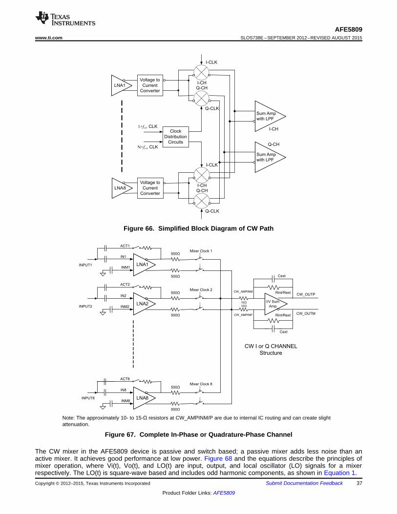
500Ω
500Ω
500Ω
500Ω
500Ω
500Ω
I/V Sum
Amp
Cext
Cext
Rint/Rext
Rint/Rext
CW_OUTM
CW_OUTP
Mixer Clock 1
Mixer Clock 2
Mixer Clock 8
LNA1
IN1
INM1
LNA2
IN2
INM2
LNA8
IN8
INM8
ACT1
ACT2
ACT8
CW I or Q CHANNEL
Structure
INPUT1
INPUT2
INPUT8
CW_AMPINP
CW_AMPINM
10Ω10Ω
Sum Amp
with LPF
LNA1
Voltage to
Current
Converter
Sum Amp
with LPF
I-CHQ-CH
I-CLK
Q-CLK
LNA8
Voltage to
Current
Converter
I-CHQ-CH
I-CLK
Q-CLK
I-CH
Q-CH
Clock
Distribution
Circuits
1×fcw CLK
N×fcw CLK
AFE5809www.ti.com SLOS738E –SEPTEMBER 2012–REVISED AUGUST 2015
Figure 66. Simplified Block Diagram of CW Path
Note: The approximately 10- to 15-Ω resistors at CW_AMPINM/P are due to internal IC routing and can create slightattenuation.
Figure 67. Complete In-Phase or Quadrature-Phase Channel
The CW mixer in the AFE5809 device is passive and switch based; a passive mixer adds less noise than anactive mixer. It achieves good performance at low power. Figure 68 and the equations describe the principles ofmixer operation, where Vi(t), Vo(t), and LO(t) are input, output, and local oscillator (LO) signals for a mixerrespectively. The LO(t) is square-wave based and includes odd harmonic components, as shown in Equation 1.Copyright © 2012–2015, Texas Instruments Incorporated Submit Documentation Feedback 37
Product Folder Links: AFE5809

2
16
p
1T
16
1T
16
10
220log
p
( ) ( )
( ) ( ) ( )
( ) ( )
0 d 0
0 0 0
d 0 d
Vi(t) sin t t t
4 1 1LO(t) sin t sin 3 t sin 5 t ...
3 5
2Vo(t) cos t cos 2 t t ...
= w + w + j + w
é ù= w + w + wê úp ë û
é ù= w + f - w - w + fë ûp
f
Vi(t) Vo(t)
LO(t)
AFE5809SLOS738E –SEPTEMBER 2012–REVISED AUGUST 2015 www.ti.com
Figure 68. Block Diagram of Mixer Operation
(1)
From Equation 1, the third-order and fifth-order harmonics from the LO can interface with the third-order and fifth-order harmonic signals in the Vi(t), or the noise around the third-order and fifth-order harmonics in the Vi(t).Therefore, the mixer’s performance is degraded. To eliminate this side effect due to the square-wavedemodulation, a proprietary harmonic-suppression circuit is implemented in the AFE5809 device. The third- andfifth-harmonic components from the LO can be suppressed by over 12 dB. Thus, the LNA output noise aroundthe third-order and fifth-order harmonic bands is not down-converted to base band. Hence, the device achieves
better noise figure. The conversion loss of the mixer is about –4 dB, which is derived from .
The mixed current outputs of the eight channels are summed together internally. An internal low-noiseoperational amplifier is used to convert the summed current to a voltage output. The internal summing amplifier isdesigned to accomplish low-power consumption, low noise, and ease of use. CW outputs from multiple AFE5809devices can be further combined on system board to implement a CW beamformer with more than eightchannels. See Typical Application for more detailed information.
Multiple clock options are supported in the AFE5809 CW path. Two CW clock inputs are required: N × ƒcw clockand 1 × ƒcw clock, where ƒcw is the CW transmitting frequency and N could be 16, 8, 4, or 1. Users have theflexibility to select the most convenient system clock solution for the AFE5809 device. In the 16 × ƒcw and 8 × ƒcwmodes, the third- and fifth-harmonic suppression feature can be supported. Thus, the 16 × ƒcw and 8 × ƒcwmodes achieve better performance than the 4 × ƒcw and 1 × ƒcw modes.
8.3.5.1 16 × ƒcw ModeThe 16 × ƒcw mode achieves the best phase accuracy compared to other modes. It is the default mode for CWoperation. In this mode, 16 × ƒcw and 1 × ƒcw clocks are required. 16 × ƒcw generates LO signals with 16accurate phases. Multiple AFE5809 devices can be synchronized by the 1 × ƒcw , that is LO signals in multipleAFEs can have the same starting phase. The phase noise specification is critical only for 16× clock. The 1× clockis for synchronization only and does not require low phase noise. See the phase noise requirement in TypicalApplication.
Figure 69 shows the top-level clock distribution diagram. Each mixer's clock is distributed through a 16 × 8 cross-point switch. The inputs of the cross-point switch are 16 different phases of the 1× clock. TI recommends aligningthe rising edges of the 1 × ƒcw and 16 × ƒcw clocks.
The cross-point switch distributes the clocks with appropriate phase delay to each mixer. For example, Vi(t) is a
received signal with a delay of , a delayed LO(t) should be applied to the mixer to compensate for the
delay. Thus a 22.5⁰ delayed clock, that is , is selected for this channel. The mathematic calculation isexpressed in the following equations:
38 Submit Documentation Feedback Copyright © 2012–2015, Texas Instruments Incorporated
Product Folder Links: AFE5809

1X Clock
Phase 337.5º
16-to-8 Cross Point Switch
1X Clock
Phase 0º
1X Clock
Phase 22.5º
1X Clock
Phase 315º
1X Clock
Phase 292.5º
Mixer 1
1X Clock
Mixer 2
1X Clock
Mixer 3
1X Clock
Mixer 6
1X Clock
Mixer 7
1X Clock
Mixer 8
1X Clock
Fin 16X Clock
SPI
D Q
Fin 1X Clock
INV
16 Phase Generator
Fin 1X Clock
[ ]
[ ]
( ) ( )
0 d 0 d
0
0 0
0
d n
1Vi(t) sin t t sin t 22.5 t
16
4 1 4LO(t) sin t sin t 22.5
16
2Vo(t) cos t t
é ùæ ö= w + + w = w + ° + wê úç ÷
ê úè øë û
é ùæ ö= w + = w + °ê úç ÷
p pê úè øë û
= w + wp
f
f
f
AFE5809www.ti.com SLOS738E –SEPTEMBER 2012–REVISED AUGUST 2015
(2)
Vo(t) represents the demodulated Doppler signal of each channel. When the Doppler signals from N channelsare summed, the signal-to-noise ratio improves.
Figure 69.
Copyright © 2012–2015, Texas Instruments Incorporated Submit Documentation Feedback 39
Product Folder Links: AFE5809
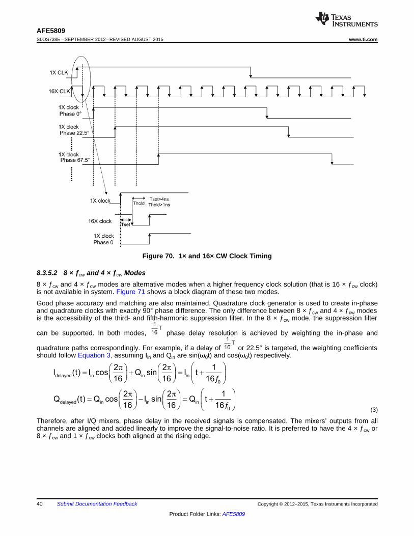
delayed in in in
0
delayed in in in
0
2 2 1I (t) I cos Q sin I t
16 16 16
2 2 1Q (t) Q cos I sin Q t
16 16 16
æ öp pæ ö æ ö= + = +ç ÷ç ÷ ç ÷
è ø è ø è ø
æ öp pæ ö æ ö= - = +ç ÷ç ÷ ç ÷
è ø è ø è ø
f
f
1T
16
1T
16
AFE5809SLOS738E –SEPTEMBER 2012–REVISED AUGUST 2015 www.ti.com
Figure 70. 1× and 16× CW Clock Timing
8.3.5.2 8 × ƒcw and 4 × ƒcw Modes8 × ƒcw and 4 × ƒcw modes are alternative modes when a higher frequency clock solution (that is 16 × ƒcw clock)is not available in system. Figure 71 shows a block diagram of these two modes.
Good phase accuracy and matching are also maintained. Quadrature clock generator is used to create in-phaseand quadrature clocks with exactly 90° phase difference. The only difference between 8 × ƒcw and 4 × ƒcw modesis the accessibility of the third- and fifth-harmonic suppression filter. In the 8 × ƒcw mode, the suppression filter
can be supported. In both modes, phase delay resolution is achieved by weighting the in-phase and
quadrature paths correspondingly. For example, if a delay of or 22.5° is targeted, the weighting coefficientsshould follow Equation 3, assuming Iin and Qin are sin(ω0t) and cos(ω0t) respectively.
(3)
Therefore, after I/Q mixers, phase delay in the received signals is compensated. The mixers’ outputs from allchannels are aligned and added linearly to improve the signal-to-noise ratio. It is preferred to have the 4 × ƒcw or8 × ƒcw and 1 × ƒcw clocks both aligned at the rising edge.
40 Submit Documentation Feedback Copyright © 2012–2015, Texas Instruments Incorporated
Product Folder Links: AFE5809

I/Q CLK
Generator
4X/8X Clock
D Q
INV
1X Clock
LNA1
Weight
Weight
Weight
Weight
LNA2~8
In-phaseCLK
QuadratureCLK
I/V
I/V
SummedIn-Phase
SummedQuadrature
AFE5809www.ti.com SLOS738E –SEPTEMBER 2012–REVISED AUGUST 2015
Figure 71. 8 × ƒcw and 4 × ƒcw Block Diagram
Figure 72. 8 × ƒcw and 4 × ƒcw Timing Diagram
Copyright © 2012–2015, Texas Instruments Incorporated Submit Documentation Feedback 41
Product Folder Links: AFE5809

LNA1
Weight
Weight
Weight
Weight
LNA2~8
In-phase
CLK
Quadrature
CLKI/V
I/V
SummedIn-Phase
SummedQuadrature
Syncronized I/Q
CLOCKs
1T
16
AFE5809SLOS738E –SEPTEMBER 2012–REVISED AUGUST 2015 www.ti.com
8.3.5.3 1 × ƒcw Mode
The 1 × ƒcw mode requires in-phase and quadrature clocks with low phase noise specifications. The phasedelay resolution is also achieved by weighting the in-phase and quadrature signals as described in the 8 × ƒcwand 4 × ƒcw modes.
Figure 73. Block Diagram of 1 x ƒcw mode
8.3.6 Digital I/Q DemodulatorThe AFE5809 device also includes a digital in-phase and quadrature (I/Q) demodulator and a low-passdecimation filter. The main purpose of the demodulation block is to reduce the LVDS data rate and improveoverall system power efficiency. The I/Q demodulator accepts ADC output with up to 65-MSPS sampling rateand 14-bit resolution. For example, after digital demodulation and 4× decimation filtering, the data rate for eitherin-phase or quadrature output is reduced to 16.25 MSPS, and the data resolution is improved to 16 bitsconsequently. Hence, the overall LVDS trace reduction can be a factor of 2. This demodulator can be bypassedand powered down completely if it is not needed.
The digital demodulator block given in the AFE5809 device is designed to do down-conversion followed bydecimation. The top-level block is divided into two exactly similar blocks: (1) subchip0 and (2) subchip1. Bothsubchips share four channels each, that is, subchip0 (ADC.1, ADC.2, ADC.3, and ADC.4) and subchip1 (ADC.5,ADC.6, ADC.7, and ADC.8).
42 Submit Documentation Feedback Copyright © 2012–2015, Texas Instruments Incorporated
Product Folder Links: AFE5809
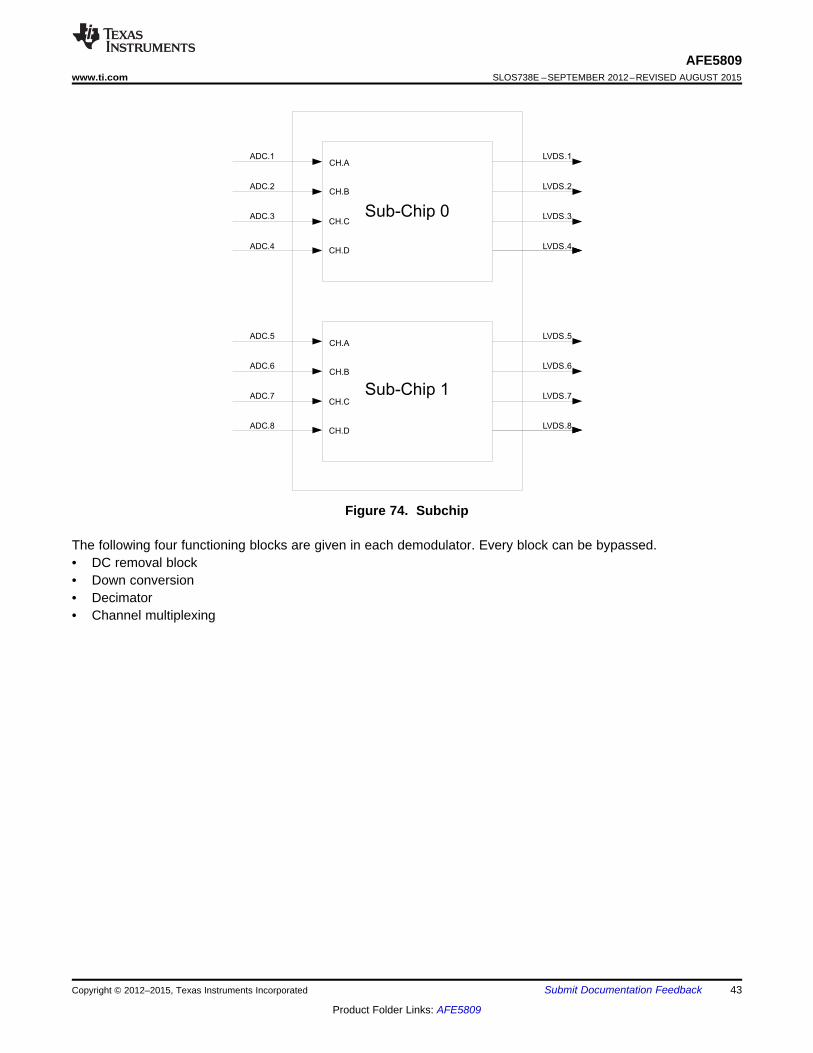
LVDS.2
LVDS.3
LVDS.4
ADC.2
ADC.3
ADC.4
Sub-Chip 0
Sub-Chip 1
LVDS.1
LVDS.6
LVDS.7
LVDS.8
LVDS.5
ADC.1
ADC.6
ADC.7
ADC.8
ADC.5
CH.A
CH.B
CH.C
CH.D
CH.A
CH.B
CH.C
CH.D
AFE5809www.ti.com SLOS738E –SEPTEMBER 2012–REVISED AUGUST 2015
Figure 74. Subchip
The following four functioning blocks are given in each demodulator. Every block can be bypassed.• DC removal block• Down conversion• Decimator• Channel multiplexing
Copyright © 2012–2015, Texas Instruments Incorporated Submit Documentation Feedback 43
Product Folder Links: AFE5809

M
M
DC
Off
set
Cos
ωt
-Sin
ωt
DC Removal Block
Down Conversion(I Phase)
Down Conversion
(Q Phase)
Decimator
DecimationFilter
Down
Sampler
Decimator
Down
SamplerDecimation
Filter
To Channel
Multiplexing
To Channel
Multiplexing
Channel A
A.I
A.Q
AFE5809SLOS738E –SEPTEMBER 2012–REVISED AUGUST 2015 www.ti.com
Figure 75. Digital Demodulator Block
1. DC removal block is used to remove DC offset. An offset value can be given to a specific register.2. Down conversion or demodulation of signal is done by multiplying signal by cos(ω0t) and by –sin(ω0t) to give
out I phase and Q phase, respectively. cos(ωt) and –sin(ωt) are 14-bit wide plus a sign bit. ω = 2πƒ, ƒ canbe set with resolution Fs / 216, where Fs is the ADC sampling frequency.
NOTEThe digital demodulator is based on a conventional down converter, that is, –sin(ω0t) isused for Q phase.
3. The decimator block has two functions: decimation filter and down sampler. Decimation filter is a variablecoefficient symmetric FIR filter and its coefficients can be given using coefficient RAM. Number of taps of FIRfilter is 16× decimation factor (M). For decimation factor of M, 8M coefficients must be stored in thecoefficient bank. Each coefficient is 14-bit wide. Down-sampler gives out 1 sample followed by M – 1samples zeros.
4. In Figure 76, channel multiplexing is implemented for flexible data routing:
44 Submit Documentation Feedback Copyright © 2012–2015, Texas Instruments Incorporated
Product Folder Links: AFE5809

S0492-01
(a) INP (b) INM (c) ACT
CM CM
Single Channel
Demodulator Blocks
Single Channel
Demodulator Blocks
Single Channel
Demodulator Blocks
Single Channel
Demodulator Blocks
M
H
A
N
N
E
L
U
X
I
N
G
C
L
T
I
P
L
E
Channel A
Channel B
Channel C
Channel D
A.I
A.Q
B.I
B.Q
C.I
C.Q
D.I
D.Q
Serializer
Serializer
Serializer
Serializer
ADC.1
DEMOD.1
ADC.2
DEMOD.2
ADC.3
DEMOD.3
DEMOD.4
ADC.4
LVDS.1
LVDS.2
LVDS.3
LVDS.4
14bits
16bits
16bits
16bits
ADC.1
ADC.2
ADC.3
ADC.4
14bits
14bits
14bits
16bits
16bits
16bits
16bits
16bits
AFE5809www.ti.com SLOS738E –SEPTEMBER 2012–REVISED AUGUST 2015
Figure 76. Channel Multiplexing
8.3.7 Equivalent Circuits
Figure 77. Equivalent Circuits of LNA Inputs
Copyright © 2012–2015, Texas Instruments Incorporated Submit Documentation Feedback 45
Product Folder Links: AFE5809

S0494-01
(a) CW 1X and 16X Clocks (b) ADC Input Clocks
CLKP
CLKM
5 kΩ 5 kΩ
VCM
S0493-01
AFE5809SLOS738E –SEPTEMBER 2012–REVISED AUGUST 2015 www.ti.com
Figure 78. Equivalent Circuits of VCNTLP/M
Figure 79. Equivalent Circuits of Clock Inputs
46 Submit Documentation Feedback Copyright © 2012–2015, Texas Instruments Incorporated
Product Folder Links: AFE5809

OUTP
OUTM
Hig
h
Hig
hL
ow
Low
AFE5809
Rout–VdiffVcommon
+Vdiff+
++
–
––
External
100- LoadW
Switch impedance is
nominally 50 ( 10%)W ±
S0495-01
(a) CW_OUTP/M (b) CW_AMPINP/M
AFE5809www.ti.com SLOS738E –SEPTEMBER 2012–REVISED AUGUST 2015
Figure 80. Equivalent Circuits of CW Summing Amplifier Inputs and Outputs
Figure 81. Equivalent Circuits of LVDS Outputs
8.3.8 LVDS Output Interface DescriptionThe AFE5809 device has a LVDS output interface, which supports multiple output formats. The ADC resolutionscan be configured as 12 bit or 14 bit as shown in the LVDS timing diagrams (Figure 1). The ADCs in theAFE5809 device are running at 14 bits; 2 LSBs are removed when 12-bit output is selected; and two zeros areadded at LSBs when 16-bit output is selected. Appropriate ADC resolutions can be selected for optimizingsystem-performance cost effectiveness. When the devices run at 16-bit mode, higher-end FPGAs are required toprocess the higher rate of LVDS data. Corresponding register settings are listed in Table 4.
Copyright © 2012–2015, Texas Instruments Incorporated Submit Documentation Feedback 47
Product Folder Links: AFE5809

AFE5809SLOS738E –SEPTEMBER 2012–REVISED AUGUST 2015 www.ti.com
8.4 Device Functional ModesThe AFE5809 device is a highly-integrated AFE solution. The AFE5809 device has two functional modes:pulsed-wave imaging mode and continous-wave Doppler imaging mode. When the AFE5809 device operates inthe pulsed-wave imaging mode, LNA, VCAT, PGA, LPF, 14-bit ADC, and digital I/Q demodulator are active. Inthe CWD imaging mode, only LNA and CW mixer are enabled. Either mode can be enabled or programmed bythe registers described below.
8.5 Programming
8.5.1 Serial Peripheral Interface (SPI) OperationThe AFE5809 device has two SPIs. The demodulator SPI interface is independent from the ADC/VCA SPI asshown in Figure 82. SPI_DIG_EN is used to select ADC/VCA SPI (SPI_DIG_EN='1') or demod SPI(SPI_DIG_EN='0').
Figure 82. SPI Interface in the AFE5809 Device
8.5.1.1 ADC/VCA Serial Register Write DescriptionProgramming of different modes can be done through the serial interface formed by pins SEN (serial interfaceenable), SCLK (serial interface clock), SDATA (serial interface data), and RESET. All these pins have a pulldownresistor to GND of 20 kΩ. Serial shift of bits into the device is enabled when SEN is low. Serial data, SDATA, islatched at every rising edge of SCLK when SEN is active (low). The serial data is loaded into the register atevery 24th SCLK rising edge when SEN is low. If the word length exceeds a multiple of 24 bits, the excess bitsare ignored. Data can be loaded in multiple of 24-bit words within a single active SEN pulse (an internal countercounts groups of 24 clocks after the falling edge of SEN). The interface can work with the SCLK frequency from20 MHz to low speeds (of a few Hertz) and even with non-50% duty cycle SCLK. The data is divided into twomain portions: a register address (8 bits) and the data itself (16 bits), to load on the addressed register. Whenwriting to a register with unused bits, set these to 0. Figure 83 shows this process.
48 Submit Documentation Feedback Copyright © 2012–2015, Texas Instruments Incorporated
Product Folder Links: AFE5809

D15 D14 D13 D12 D11 D10 D9 D8 D7 D6 D5 D4 D3 D2 D1 D0A7 A6 A5 A4 A3 A2 A1 A0
SEN
SCLK
SDATA
RESET
Data Latched On Rising Edge of SCLK
Start Sequence
Start Sequence
End Sequence
End Sequence
t7
t6
t2
t4
t1
t5
t3
T0384-01
AFE5809www.ti.com SLOS738E –SEPTEMBER 2012–REVISED AUGUST 2015
Programming (continued)
Figure 83. SPI Timing
NOTETI recommends synchronizing SCLK to ADC CLK. Typically, SCLK can be generated bydividing ADC CLK by an integer factor of N. In a system with multiple AFEs, SCLKs maynot reach all AFEs simultaneously due to routing. To compensate routing differences andensure AFEs’ outputs are aligned, SCLK can be adjusted to toggle on either the fallingedge of ADCLK or the rising edge of ADC CLK (ensuring new register settings are loadedbefore next ADC sampling clock).
8.5.1.2 ADC/VCA Serial Register Readout DescriptionThe device includes an option where the contents of the internal registers can be read back. This may be usefulas a diagnostic test to verify the serial interface communication between the external controller and the AFE.First, the <REGISTER READOUT ENABLE> bit (Reg0[1]) needs to be set to 1. Then, the user should initiate aserial interface cycle specifying the address of the register (A7 through A0) whose content must be read. Thedata bits are don’t care. The device outputs the contents (D15 through D0) of the selected register on theSDOUT pin. SDOUT has a typical delay, t8, of 20 ns from the falling edge of the SCLK. For lower speed SCLK,SDOUT can be latched on the rising edge of SCLK. For higher speed SCLK, for example, if the SCLK period isless than 60 ns, it is better to latch the SDOUT at the next falling edge of SCLK. Figure 84 shows this operation(the timing specifications follow the same information provided). In the readout mode, users still can access the<REGISTER READOUT ENABLE> through SDATA/SCLK/SEN. To enable serial register writes, set the<REGISTER READOUT ENABLE> bit back to 0.
The AFE5809 SDOUT buffer is tri-stated and gets enabled only when 0[1] (REGISTER READOUT ENABLE) isenabled. SDOUT pins from multiple AFE5809 devices can be tied together without any pullup resistors. Levelshifter SN74AUP1T04 can be used to convert 1.8-V logic to 2.5-V/3.3-V logics if needed.
Copyright © 2012–2015, Texas Instruments Incorporated Submit Documentation Feedback 49
Product Folder Links: AFE5809

x x x x x x x x x x x x x x x xA7 A6 A5 A4 A3 A2 A1 A0
SEN
SCLK
SDATA
SDOUT
Start Sequence End Sequence
t7
t6
t2
t4
t1
t5
t3
D15 D14 D13 D12 D11 D10 D9 D8 D7 D6 D5 D4 D3 D2 D1 D0
t8
AFE5809SLOS738E –SEPTEMBER 2012–REVISED AUGUST 2015 www.ti.com
Programming (continued)
Figure 84. Serial Interface Register Read
8.5.1.3 Digital Demodulator SPI DescriptionDemodulator is enabled after a software or hardware reset. It can be disabled by setting the LSB of register 0x16as 1. This is done using the ADC SPI interface, that is, SPI_DIG_EN = 1.
To access the specific demodulator registers:1. SPI_DIG_EN pin is required to be set as 0 during SPI transactions to demodulator registers. Meanwhile,
ADC SEN needs to be set as 0 during demodulator SPI programming.2. The SPI register address is 8 bits and is made of 2 subchip select bits and 6 register address bits. SPI
register data is 16 bits.
Table 2. Register Address Bit DescriptionBit7 Bit6 Bit 5:0SCID1_SEL SCID0_SEL Register address <5:0>
3. SCID0_SEL enables configuration of channels 1 through 4. SCID1_SEL enables configuration of channels 5through 8. When performing demodulator SPI write transactions, these SCID bits can be individually ormutually used with a specific register address.
4. Register configuration is normally shared by both subchips (both SCID bits should be set as 1). An exceptionto this rule would be the DC OFFSET registers (0x14 through 0x17) for which specific channel access isexpected.
50 Submit Documentation Feedback Copyright © 2012–2015, Texas Instruments Incorporated
Product Folder Links: AFE5809

LVDS.2
LVDS.3
LVDS.4
ADC.2
ADC.3
ADC.4
Sub-Chip 0
Sub-Chip 1
LVDS.1
LVDS.6
LVDS.7
LVDS.8
LVDS.5
ADC.1
ADC.6
ADC.7
ADC.8
ADC.5
CH.A
CH.B
CH.C
CH.D
CH.A
CH.B
CH.C
CH.D
AFE5809www.ti.com SLOS738E –SEPTEMBER 2012–REVISED AUGUST 2015
A. Each of two subchips supports four channels.B. Each of two demodulators has four channels named as A, B, C, and D.
Figure 85. Demod Subchip 0 and Subchip 1
5. Demodulator register readout follows these procedures:– Write 1 to register 0x0[1]; pin SPI_DIG_EN should be 0 while writing. This is the readout enable register
for demodulator.– Write 1 to register 0x0[1]; pin SPI_DIG_EN should be 1 while writing. This is the readout enable register
for ADC and VCA.– Set SPI_DIG_EN as 0 and write anything to the register whose stored data needs to be known. Device
finds the address of the register and sends its stored data at the SDOUT pin serially.
NOTEAfter enabling the register 0x0[1] REGISTER_READOUT_ENABLE, data cannot bewritten to the register (whose data needs to be known), but stored data would comeserially at the SDOUT pin.
– To disable the register readout, first write 0 to register 0x0[1] while SPI_DIG_EN is 1; then write 0 toregister 0x0[1] while SPI_DIG_EN is 0.
Copyright © 2012–2015, Texas Instruments Incorporated Submit Documentation Feedback 51
Product Folder Links: AFE5809

AFE5809SLOS738E –SEPTEMBER 2012–REVISED AUGUST 2015 www.ti.com
8.6 Register Maps
8.6.1 ADC and VCA Register DescriptionA reset process is required at the AFE5809 device's initialization stage. Initialization can be done in one of twoways:• Through a hardware reset, by applying a positive pulse in the RESET pin.• Through a software reset, using the serial interface, by setting the SOFTWARE RESET bit to high. Setting
this bit initializes the internal registers to the respective default values (all zeros), and then self-resets theSOFTWARE RESET bit to low. In this case, the RESET pin can stay low (inactive).
After reset, all ADC and VCA registers are set to 0, that is default setting. During register programming, allunlisted register bits must be set as 0.
Some demodulator registers are set as 1 after reset. During register programming, all unlisted register bits mustbe set as 0. In addition, the demodulator registers can be reset when 0x16[0] is set as 0. Thus, it is required toreconfigure the demodulator registers after toggling the 0x16[0] from 1 to 0.
8.6.1.1 ADC Register Map
Address Address Default Function Description(DEC) (HEX) Value
0: Normal operation0[0] 0x0[0] 0 SOFTWARE_RESET 1: Resets the device and self-clears the bit to 0. Note: Register 0 is a write
only register.
0:Disables readout1: Enables readout of register at SDOUT pin. Note: When this bit is set to 0,
0[1] 0x0[1] 0 REGISTER_READOUT_ENABLE the device always operates in write mode and when it is set to 1, device will bein read mode. Multiple reading or writing events can be performed when thisbit is set to 1 or 0 correspondingly. Register 0 is a write-only register.
0: Normal1: Complete power down. Note: When the complete power-down mode is
1[0] 0x1[0] 0 ADC_COMPLETE_PDN enabled, the digital demodulator may lose register settings. Therefore, it isrequired to reconfigure the demodulator registers, filter coefficient memory,and profile memory after exiting the complete power-down mode.
0: Output enabled1[1] 0x1[1] 0 LVDS_OUTPUT_DISABLE 1: Output disabled
0: Normal operation1: Power down. Power down individual ADC channels.1[9:2] 0x1[9:2] 0 ADC_PDN_CH<7:0>1[9] → CH8…1[2] → CH1
0: Normal operation1[10] 0x1[10] 0 PARTIAL_PDN 1: Partial power down ADC
LOW_FREQUENCY_ 0: No suppression1[11] 0x1[11] 0 NOISE_SUPPRESSION 1: Suppression enabled
0: Internal reference1[13] 0x1[13] 0 EXT_REF 1: External reference. VREF_IN is used. Both 3[15] and 1[13] should be set as
1 in the external reference mode
0: 1× rate1[14] 0x1[14] 0 LVDS_OUTPUT_RATE_2X 1: 2× rate. Combines data from 2 channels on 1 LVDS pair. When ADC clock
rate is low, this feature can be used.
0: Differential clock input1[15] 0x1[15] 0 SINGLE-ENDED_CLK_MODE 1: Single-ended clock input
2[2:0] 0x2[2:0] 0 RESERVED Set to 0
0: Normal operation2[10:3] 0x2[10:3] 0 POWER-DOWN_LVDS 1: PDN individual LVDS outputs. 2[10] → CH8…2[3] → CH1
0: No averaging2[11] 0x2[11] 0 AVERAGING_ENABLE 1: Average two channels to increase SNR
0: Default latency with digital features supported2[12] 0x2[12] 0 LOW_LATENCY 1: Low latency with digital features bypassed
52 Submit Documentation Feedback Copyright © 2012–2015, Texas Instruments Incorporated
Product Folder Links: AFE5809

AFE5809www.ti.com SLOS738E –SEPTEMBER 2012–REVISED AUGUST 2015
Register Maps (continued)Address Address Default Function Description(DEC) (HEX) Value
000: Normal operation001: Sync010: De-skew011: Custom2[15:13] 0x2[15:13] 0 TEST_PATTERN_MODES 100:All 1's101: Toggle110: All 0's111: Ramp
0: No inverting1: Invert channel digital output. 3[7] → CH8;3[0] → CH1. Note: Suppose that
3[7:0] 0x3[7:0] 0 INVERT_CHANNELS the device is giving digital output of 11001100001111. After enabling this bit,output of device becomes 00110011110000. Note: This function is notapplicable for ADC test patterns and in demod mode.
0: No offset subtractionCHANNEL_OFFSET_3[8] 0x3[8] 0 SUBSTRACTION_ENABLE 1: Offset value subtract enabled
3[9:11] 0x3[9:11] 0 RESERVED Set to 0
0: No digital gain3[12] 0x3[12] 0 DIGITAL_GAIN_ENABLE 1: Digital gain enabled
Serialization factor00: 14×01: 16×10: Reserved
3[14:13] 0x3[14:13] 0 SERIALIZED_DATA_RATE 11: 12×When 4[1] = 1, in the 16× serialization rate, two zeros are filled at two LSBs(see Table 4). Note: Make sure the settings aligning with the demod register0x3[14:13]. Be aware that the same setting, for example, 00, in these tworegisters can represent different LVDS data rates respectively.
0: Internal reference modeENABLE_EXTERNAL_ 1: Set to external reference mode3[15] 0x3[15] 0 REFERENCE_MODE Note: Both 3[15] and 1[13] should be set as 1 when configuring the device in
the external reference mode.
0: 14 bit4[1] 0x4[1] 0 ADC_RESOLUTION_SELECT 1: 12 bit
0: 2's complement1: Offset binary4[3] 0x4[3] 0 ADC_OUTPUT_FORMAT Note: When the demodulation feature is enabled, only 2's complementformat can be selected.
0: LSB first4[4] 0x4[4] 0 LSB_MSB_FIRST 1: MSB first
5[13:0] 0x5[13:0] 0 CUSTOM_PATTERN Custom pattern data for LVDS output (2[15:13] = 011)
0: Test pattern outputs of 8 channels are not synchronized.10[8] 0xA[8] 0 SYNC_PATTERN 1: Test pattern outputs of 8 channels are synchronized.
13[9:0] 0xD[9:0] 0 OFFSET_CH1 Value to be subtracted from channel 1 code
13[15:11] 0xD[15:11] 0 DIGITAL_GAIN_CH1 0 to 6 dB in 0.2-dB steps
15[9:0] 0xF[9:0] 0 OFFSET_CH2 Value to be subtracted from channel 2 code
15[15:11] 0xF[15:11] 0 DIGITAL_GAIN_CH2 0 to 6 dB in 0.2-dB steps
17[9:0] 0x11[9:0] 0 OFFSET_CH3 Value to be subtracted from channel 3 code
17[15:11] 0x11[15:11] 0 DIGITAL_GAIN_CH3 0 to 6 dB in 0.2-dB steps
19[9:0] 0x13[9:0] 0 OFFSET_CH4 Value to be subtracted from channel 4 code
19[15:11] 0x13[15:11] 0 DIGITAL_GAIN_CH4 0 to 6 dB in 0.2-dB steps
0: Disable the digital HPF filter;DIGITAL_HPF_FILTER_ENABLE 1: Enable for 1 to 4 channels21[0] 0x15[0] 0 _ CH1-4 Note: This HPF feature is only available when the demodulation block is
disabled.
Set K for the HPF (k from 2 to 10, that is 0010B to 1010B).This group of four registers controls the characteristics of a digital high-pass21[4:1] 0x15[4:1] 0 DIGITAL_HPF_FILTER_K_CH1-4 transfer function applied to the output data, following the formula:y(n) = 2k/(2k + 1) [x(n) – x(n – 1) + y(n – 1)] (see Table 3)
Copyright © 2012–2015, Texas Instruments Incorporated Submit Documentation Feedback 53
Product Folder Links: AFE5809

Digital OffsetDefault=No
ADCOutput 12/14b
FinalDigitalOutput12/14b
DigitalGain
Default=0
ChannelAverage
Default=No
Digital HPFDefault = No
AFE5809SLOS738E –SEPTEMBER 2012–REVISED AUGUST 2015 www.ti.com
Register Maps (continued)Address Address Default Function Description(DEC) (HEX) Value
0: Digital demodulator is enabled1: Digital demodulator is disabled
22[0] 0x16[0] 0 EN_DEMOD Note: The demodulator registers can be reset when 0x16[0] is set as 0. Thus,it is required to reconfigure the demodulator registers after toggling the0x16[0].
25[9:0] 0x19[9:0] 0 OFFSET_CH8 Value to be subtracted from channel 8 code
25[15:11] 0x19[15:11] 0 DIGITAL_GAIN_CH8 0 to 6-dB in 0.2-dB steps
27[9:0] 0x1B[9:0] 0 OFFSET_CH7 Value to be subtracted from channel 7 code
27[15:11] 0x1B[15:11] 0 DIGITAL_GAIN_CH7 0 to 6-dB in 0.2-dB steps
29[9:0] 0x1D[9:0] 0 OFFSET_CH6 Value to be subtracted from channel 6 code
29[15:11] 0x1D[15:11] 0 DIGITAL_GAIN_CH6 0 to 6-dB in 0.2-dB steps
31[9:0] 0x1F[9:0] 0 OFFSET_CH5 Value to be subtracted from channel 5 code
31[15:11] 0x1F[15:11] 0 DIGITAL_GAIN_CH5 0 to 6-dB in 0.2-dB steps
0: Disable the digital HPF filterDIGITAL_HPF_FILTER_ENABLE 1: Enable for 5 to 8 channels33[0] 0x21[0] 0 _ CH5-8 Note: This HPF feature is only available when the demodulation block is
disabled.
Set K for the HPF (k from 2 to 10, 0010B to 1010B)This group of four registers controls the characteristics of a digital high-pass33[4:1] 0x21[4:1] 0 DIGITAL_HPF_FILTER_K_CH5-8 transfer function applied to the output data, following the formula:y(n) = 2k / (2k + 1) [x(n) – x(n – 1) + y(n – 1)] (see Table 3)
8.6.1.2 AFE5809 ADC Register/Digital Processing DescriptionThe ADC in the AFE5809 device has extensive digital processing functionality, which can be used to enhanceultrasound system performance. The digital processing blocks are arranged as in Figure 86.
Figure 86. ADC Digital Block Diagram
NOTEThese digital processing features are only available when the demodulation block isdisabled. ADC output data directly enter the digital demodulator when the demod isenabled.
8.6.1.2.1 AVERAGING_ENABLE: Address: 2[11]
When set to 1, two samples, corresponding to two consecutive channels, are averaged (channel 1 with 2, 3 with4, 5 with 6, and 7 with 8). If both channels receive the same input, the net effect is an improvement in SNR. Theaveraging is performed as:• Channel 1 + channel 2 comes out on channel 3• Channel 3 + channel 4 comes out on channel 4• Channel 5 + channel 6 comes out on channel 5• Channel 7 + channel 8 comes out on channel 6
54 Submit Documentation Feedback Copyright © 2012–2015, Texas Instruments Incorporated
Product Folder Links: AFE5809

( ) ( ) ( ) ( )2
k
k
2y n = x n x n 1 y n 1
1é ù- - + -ë û+
AFE5809www.ti.com SLOS738E –SEPTEMBER 2012–REVISED AUGUST 2015
8.6.1.2.2 ADC_OUTPUT_FORMAT: Address: 4[3]
The ADC output, by default, is in 2’s-complement mode. Programming the ADC_OUTPUT_FORMAT bit to 1inverts the MSB, and the output becomes straight-offset binary mode.
NOTEWhen the demodulation feature is enabled, only 2's complement format can be selected.
8.6.1.2.3 ADC Reference Mode: Address 1[13] and 3[15]
The following shows the register settings for the ADC internal reference mode and external reference mode.• 0x1[13] 0x3[15] = 00: ADC internal reference mode, VREF_IN floating (pin M3)• 0x1[13] 0x3[15] = 01: N/A• 0x1[13] 0x3[15] = 10: N/A• 0x1[13] 0x3[15] = 11: ADC external reference mode, VREF_IN = 1.4 V (pin M3)
8.6.1.2.4 DIGITAL_GAIN_ENABLE: Address: 3[12]
Setting this bit to 1 applies to each channel i the corresponding gain given by DIGTAL_GAIN_CHi <15:11>. Thegain is given as 0 dB + 0.2 dB × DIGTAL_GAIN_CHi<15:11>. For instance, if DIGTAL_GAIN_CH5<15:11> = 3,channel 5 is increased by 0.6-dB gain. DIGTAL_GAIN_CHi <15:11> = 31 produces the same effect asDIGTAL_GAIN_CHi <15:11> = 30, setting the gain of channel i to 6 dB.
8.6.1.2.5 DIGITAL_HPF_ENABLE• CH1 to CH4: Address 21[0]• CH5 to CH8: Address 33[0]
8.6.1.2.6 DIGITAL_HPF_FILTER_K_CHX• CH1 to CH4: Address 21[4:1]• CH5 to CH8: Address 33[4:1]
This group of registers controls the characteristics of a digital high-pass transfer function applied to the outputdata, following Equation 4.
(4)
These digital HPF registers (one for the first four channels and one for the second group of four channels)describe the setting of K. The digital HPF can be used to suppress low frequency noise, which commonly existsin ultrasound echo signals. The digital filter can significantly benefit near-field recovery time due to T/R switchlow-frequency response. Table 3 shows the cut-off frequency versus K.
Table 3. Digital HPF –1-dB Corner Frequency versus K and Fsk 40 MSPS 50 MSPS 65 MSPS2 2780 kHz 3480 kHz 4520 kHz3 1490 kHz 1860 kHz 2420 kHz4 770 kHz 960 kHz 1250 kHz
8.6.1.2.7 LOW_FREQUENCY_NOISE_SUPPRESSION: Address: 1[11]
The low-frequency noise suppression mode is especially useful in applications where good noise performance isdesired in the frequency band of 0 to 1 MHz (around DC). Setting this mode shifts the low-frequency noise of theAFE5809 device to approximately Fs / 2, thereby moving the noise floor around DC to a much lower value.Register bit 1[11] is used for enabling or disabling this feature. When this feature is enabled, power consumptionof the device is increased slightly by approximately 1 mW/CH.
Copyright © 2012–2015, Texas Instruments Incorporated Submit Documentation Feedback 55
Product Folder Links: AFE5809

AFE5809SLOS738E –SEPTEMBER 2012–REVISED AUGUST 2015 www.ti.com
8.6.1.2.8 LVDS_OUTPUT_RATE_2X: Address: 1[14]
The output data always uses a DDR format, with valid/different bits on the positive as well as the negative edgesof the LVDS bit clock, DCLK. The output rate is set by default to 1× (LVDS_OUTPUT_RATE_2X = 0), whereeach ADC has one LVDS stream associated with it. If the sampling rate is low enough, two ADCs can share oneLVDS stream, in this way lowering the power consumption devoted to the interface. The unused outputs willoutput zero. To avoid consumption from those outputs, no termination should be connected to them. Thedistribution on the used output pairs is done in the following way:• Channel 1 and channel 2 come out on channel 3. Channel 1 comes out first.• Channel 3 and channel 4 come out on channel 4. Channel 3 comes out first.• Channel 5 and channel 6 come out on channel 5. Channel 5 comes out first.• Channel 7 and channel 8 come out on channel 6. Channel 7 comes out first.
8.6.1.2.9 CHANNEL_OFFSET_SUBSTRACTION_ENABLE: Address: 3[8]
Setting this bit to 1 enables the subtraction of the value on the corresponding OFFSET_CHx<9:0> (offset forchannel i) from the ADC output. The number is specified in 2's complement format. For example,OFFSET_CHx<9:0> = 11 1000 0000 means subtract –128. For OFFSET_CHx<9:0> = 00 0111 1111 the effect isto subtract 127. In effect, both addition and subtraction can be performed. The offset is applied before the digitalgain (see DIGITAL_GAIN_ENABLE). The whole data path is 2's complement throughout internally, with digitalgain being the last step. Only when ADC_OUTPUT_FORMAT = 1 (straight binary output format) is the 2'scomplement word translated into offset binary at the end.
8.6.1.2.10 SERIALIZED_DATA_RATE: Address: 3[14:13]
See Table 4 for detailed description.
Table 4. Corresponding Register SettingsLVDS Rate 12 bit (6× DCLK) 14 bit (7× DCLK) 16 bit (8× DCLK)
Register 3 [14:13] 11 00 01Register 4 [2:0] 010 000 000
Description 2 LSBs removed N/A 2 zeroes added at LSBs
8.6.1.2.11 TEST_PATTERN_MODES: Address: 2[15:13]
The AFE5809 device can output a variety of test patterns on the LVDS outputs. These test patterns replace thenormal ADC data output. The device may also be made to output 6 preset patterns:• Ramp: Setting Register 2[15:13] = 111 causes all the channels to output a repeating full-scale ramp pattern.
The ramp increments from zero code to full-scale code in steps of 1 LSB every clock cycle. After hitting thefull-scale code, it returns back to zero code and ramps again.
• Zeros: The device can be programmed to output all 0 s by setting Register 2[15:13] = 110.• Ones: The device can be programmed to output all 1 s by setting Register 2[15:13] = 100.• Deskew Patten: When 2[15:13] = 010; this mode replaces the 14-bit ADC output with the 01010101010101
word.• Sync Pattern: When 2[15:13] = 001, the normal ADC output is replaced by a fixed 11111110000000 word.• Toggle: When 2[15:13] = 101, the normal ADC output is alternating from 1 s to 0 s. The start state of ADC
word can be either 1 s or 0 s.• Custom Pattern: It can be enabled when 2[15:13] = 011. Users can write the required VALUE into register bits
<CUSTOM PATTERN>, which is Register 5[13:0]. Then, the device will output VALUE at its outputs, about 3to 4 ADC clock cycles after the 24th rising edge of SCLK. So, the time taken to write one value is 24 SCLKclock cycles + 4 ADC clock cycles. To change the customer pattern value, users can repeat writing Register5[13:0] with a new value. Due to the speed limit of SPI, the refresh rate of the custom pattern may not behigh. For example, 128 points custom pattern takes approximately 128 × (24 SCLK clock cycles + 4 ADCclock cycles).
56 Submit Documentation Feedback Copyright © 2012–2015, Texas Instruments Incorporated
Product Folder Links: AFE5809

AFE5809www.ti.com SLOS738E –SEPTEMBER 2012–REVISED AUGUST 2015
NOTEOnly one of the above patterns can be active at any given instant. Test pattern from theADC output stage can NOT be sent to the demodulator; it can only be sent to the LVDSserializer when the demodulator is off.
8.6.1.2.12 SYNC_PATTERN: Address: 10[8]
By enabling this bit, all channels' test pattern outputs are synchronized. When 10[8] is set as 1, the ramppatterns of all 8 channels start simultaneously.
8.6.1.3 VCA Register Map
Address Address Default Function Description(DEC) (HEX) Value51[0] 0x33[0] 0 RESERVED 051[3:1] 0x33[3:1] 0 LPF_PROGRAMMABILITY 000: 15 MHz
010: 20 MHz011: 30 MHz100: 10 MHzNote: 0x3D[14], that is, 5 MHz LPF, should be setas 0.
51[4] 0x33[4] 0 PGA_INTEGRATOR_DISABLE 0: Enable(PGA_HPF_DISABLE) 1: Disable offset integrator for PGA. See the
explanation for the PGA integrator function in theApplication Information section
51[7:5] 0x33[7:5] 0 PGA_CLAMP_LEVEL Low-noise mode: 53[11:10] = 00000: –2 dBFS010: 0 dBFS1XX: Clamp is disabledLow-power/medium-power mode; 53[11:10] =01/10100: –2 dBFS110: 0 dBFS0XX: clamp is disabledNote: The clamp circuit makes sure that PGAoutput is in linear range. For example, at 000setting, PGA output HD3 will worsen by 3 dB at–2-dBFS ADC input. In normal operation, clampfunction can be set as 000 in the low-noise mode.The maximum PGA output level can exceed 2Vppwith the clamp circuit enabled.Note: In the low-power and medium-powermodes, PGA_CLAMP is disabled for saving powerif 51[7] = 0. .Note: Register 61[15] should be set as 0;otherwise, PGA_CLAMP_LEVEL is affected byRegister 61[15].
51[13] 0x33[13] 0 PGA_GAIN_CONTROL 0:24 dB1:30 dB
52[4:0] 0x34[4:0] 0 ACTIVE_TERMINATION_ See Table 6. Register 52[5] should be set as 1 toINDIVIDUAL_RESISTOR_CNTL access these bits
52[5] 0x34[5] 0 ACTIVE_TERMINATION_ 0: DisableINDIVIDUAL_RESISTOR_ENABLE 1: Enable internal active termination individual
resistor control52[7:6] 0x34[7:6] 0 PRESET_ACTIVE_ TERMINATIONS 00: 50 Ω
01: 100 Ω10: 200 Ω11: 400 ΩNote: The device adjusts resistor mapping(52[4:0]) automatically. 50-Ω active termination isnot supported in 12-dB LNA setting. Instead, 00represents high-impedance mode when LNA gainis 12 dB.
Copyright © 2012–2015, Texas Instruments Incorporated Submit Documentation Feedback 57
Product Folder Links: AFE5809

AFE5809SLOS738E –SEPTEMBER 2012–REVISED AUGUST 2015 www.ti.com
Address Address Default Function Description(DEC) (HEX) Value52[8] 0x34[8] 0 ACTIVE TERMINATION ENABLE 0: Disable
1: Enable active termination52[10:9] 0x34[10:9] 0 LNA_INPUT_CLAMP_SETTING 00: Auto setting
01: 1.5 Vpp10: 1.15 Vpp11: 0.6 Vpp
52[11] 0x34[11] 0 RESERVED Set to 052[12] 0x34[12] 0 LNA_INTEGRATOR_DISABLE 0: Enable
(LNA_HPF_DISABLE) 1: Disable offset integrator for LNA. See theexplanation for this function in the followingsection
52[14:13] 0x34[14:13] 0 LNA_GAIN 00: 18 dB01: 24 dB10: 12 dB11: Reserved
52[15] 0x34[15] 0 LNA_INDIVIDUAL_CH_CNTL 0: Disable1: Enable LNA individual channel control. SeeRegister 57 for details
53[7:0] 0x35[7:0] 0 PDN_CH<7:0> 0: Normal operation1: Powers down corresponding channels. Bit7 →CH8, Bit6 → CH7…Bit0 → CH1. PDN_CH shutsdown whichever blocks are active depending onTGC mode or CW mode.
53[8] 0x35[8] 0 RESERVED Set to 053[9] 0x35[9] 0 LOW_NF 0: Normal operation
1: Enable low-noise figure mode for high-impedance probes
53[11:10] 0x35[11:10] 0 POWER_MODES 00: Low noise mode01: Set to low-power mode. At 30-dB PGA, totalchain gain may slightly change. See TypicalCharacteristics.10: Set to medium-power mode. At 30-dB PGA,total chain gain may slightly change. See TypicalCharacteristics.11: Reserved
53[12] 0x35[12] 0 PDN_VCAT_PGA 0: Normal operation1: Powers down VCAT and PGA
53[13] 0x35[13] 0 PDN_LNA 0: Normal operation1: Powers down LNA only
53[14] 0x35[14] 0 VCA_PARTIAL_PDN 0: Normal operation1: Powers down LNA, VCAT, and PGA partially(fast-wake response)
53[15] 0x35[15] 0 VCA_COMPLETE_PDN 0: Normal operation1: Power down LNA, VCAT, and PGA completely(slow-wake response). This bit can overwrite53[14].
54[4:0] 0x36[4:0] 0 CW_SUM_AMP_GAIN_CNTL Select feedback resistor for the CW amplifier asper Table 6
54[5] 0x36[5] 0 CW_16X_CLK_SEL 0: Accept differential clock1: Accept CMOS clock
54[6] 0x36[6] 0 CW_1X_CLK_SEL 0: Accept CMOS clock1: Accept differential clock
54[7] 0x36[7] 0 RESERVED Set to 054[8] 0x36[8] 0 CW_TGC_SEL 0: TGC mode
1 : CW modeNote : VCAT and PGA are still working in CWmode. They should be powered down separatelythrough 53[12].
58 Submit Documentation Feedback Copyright © 2012–2015, Texas Instruments Incorporated
Product Folder Links: AFE5809

AFE5809www.ti.com SLOS738E –SEPTEMBER 2012–REVISED AUGUST 2015
Address Address Default Function Description(DEC) (HEX) Value54[9] 0x36[9] 0 CW_SUM_AMP_ENABLE 0: Enable CW summing amplifier
1: Disable CW summing amplifierNote: 54[9] is only effective in CW mode.
54[11:10] 0x36[11:10] 0 CW_CLK_MODE_SEL 00: 16× mode01: 8× mode10: 4× mode11: 1× mode
55[3:0] 0x37[3:0] 0 CH1_CW_MIXER_PHASE55[7:4] 0x37[7:4] 0 CH2_CW_MIXER_PHASE55[11:8] 0x37[11:8] 0 CH3_CW_MIXER_PHASE55[15:12] 0x37[15:12] 0 CH4_CW_MIXER_PHASE 0000 → 1111, 16 different phase delays, see
Table 1056[3:0] 0x38[3:0] 0 CH5_CW_MIXER_PHASE56[7:4] 0x38[7:4] 0 CH6_CW_MIXER_PHASE56[11:8] 0x38[11:8] 0 CH7_CW_MIXER_PHASE56[15:12] 0x38[15:12] 0 CH8_CW_MIXER_PHASE57[1:0] 0x39[1:0] 0 CH1_LNA_GAIN_CNTL 00: 18 dB
01: 24 dB57[3:2] 0x39[3:2] 0 10: 12 dBCH2_LNA_GAIN_CNTL 11: Reserved
REG52[15] should be set as 1.57[5:4] 0x39[5:4] 0 CH3_LNA_GAIN_CNTL 00: 18 dB
01: 24 dB57[7:6] 0x39[7:6] 0 CH4_LNA_GAIN_CNTL 10: 12 dB57[9:8] 0x39[9:8] 0 CH5_LNA_GAIN_CNTL 11: Reserved
REG52[15] should be set as 1.57[11:10] 0x39[11:10] 0 CH6_LNA_GAIN_CNTL57[13:12] 0x39[13:12] 0 CH7_LNA_GAIN_CNTL57[15:14] 0x39[15:14] 0 CH8_LNA_GAIN_CNTL59[3:2] 0x3B[3:2] 0 HPF_LNA 00: 100 kHz
01: 50 kHz10: 200 kHz11: 150 kHz with 0.015 µF on INMx
59[6:4] 0x3B[6:4] 0 DIG_TGC_ATT_GAIN 000: 0-dB attenuation001: 6-dB attenuationN: About N × 6 dB attenuation when 59[7] = 1
59[7] 0x3B[7] 0 DIG_TGC_ATT 0: Disable digital TGC attenuator1: Enable digital TGC attenuator
59[8] 0x3B[8] 0 CW_SUM_AMP_PDN 0: Power down1: Normal operationNote: 59[8] is only effective in TGC test mode.
59[9] 0x3B[9] 0 PGA_TEST_MODE 0: Normal CW operation1: PGA outputs appear at CW outputs.
61[13] 0x3D[13] 0 V2I_CLAMP 0: Clamp disabled1: Clamp enabled at the V2I input. An additionalvoltage clamp at the V2I input. This limits theamount of overload signal the PGA sees.Note: This bit is supported by AFE5809 with datecode later than 2014, that is, date code >41XXXX.
61[14] 0x3D[14] 0 5MHz_LPF 0: 5-MHz LPF disabled1: 5-MHz LPF enabled. Suppress signals >5 MHzor high-order harmonics. The LPF Register51[3:1] needs to be set as 100, that is, 10 MHz.Note: This bit is supported by AFE5809 with datecode later than 2014, that is date code >41XXXX.
Copyright © 2012–2015, Texas Instruments Incorporated Submit Documentation Feedback 59
Product Folder Links: AFE5809

AFE5809SLOS738E –SEPTEMBER 2012–REVISED AUGUST 2015 www.ti.com
Address Address Default Function Description(DEC) (HEX) Value61[15] 0x3D[15] 0 PGA_CLAMP_-6dBFS 0: Disable the –6-dBFS clamp. PGA_CLAMP is
set by Reg51[7:5].1: Enable the –6-dBFS clamp. PGA_CLAMPReg51[7:5] should be set as 000 in the low-noise mode or 100 in the low-power/medium-power mode. In this setting, PGA output HD3 willbe worsen by 3 dB at –6-dBFS ADC input. Theactual PGA output is reduced to approximately 1.5Vpp, about 2.5 dB below the ADC full-scale input2 Vpp . As a result, AFE5809’s LPF is notsaturated, and it can suppress harmonic signalsbetter at PGA output. Due to PGA outputreduction, the ADC output dynamic range isimpacted.Note: This bit is supported by AFE5809 withdate code later than 2014, that is date code>41XXXX.Note: This bit is ONLY valid when PGA=24dB.
8.6.1.4 VCA Register Description
8.6.1.4.1 LNA Input Impedances Configuration (Active Termination Programmability)
Different LNA input impedances can be configured through the register 52[4:0]. By enabling and disabling thefeedback resistors between LNA outputs and ACTx pins, LNA input impedance is adjustable accordingly. Table 5describes the relationship between LNA gain and 52[4:0] settings. The input impedance settings are the same forboth TGC and CW paths.
The AFE5809 device also has four preset active termination impedances as described in 52[7:6]. An internaldecoder is used to select appropriate resistors corresponding to different LNA gain.
Table 5. Register 52[4:0] Description52[4:0]/0x34[4:0] FUNCTION
00000 No feedback resistor enabled00001 Enables 450-Ω feedback resistor00010 Enables 900-Ω feedback resistor00100 Enables 1800-Ω feedback resistor01000 Enables 3600-Ω feedback resistor10000 Enables 4500-Ω feedback resistor
The input impedance of AFE can be programmed through Register 52[8:0]. Each bit of Register 52[4:0] controlsone active termination resistor. The following tables indicate the nominal impedance values when individualactive termination resistors are selected. See Active Termination for more details. Table 6 shows thecorresponding impedances under different Register 52[4:0] values, while Table 7 shows the Register 52[4:0]settings under different impedances.
NOTETable 6 and Table 7 show nominal input impedance values. Due to silicon processvariation, the actual values can vary.
Table 6. Register 52[4:0] versus LNA Input Impedances52[4:0]/0x34[4:0] 00000 00001 00010 00011 00100 00101 00110 00111LNA:12dB High Z 150 Ω 300 Ω 100 Ω 600 Ω 120 Ω 200 Ω 86 ΩLNA:18dB High Z 90 Ω 180 Ω 60 Ω 360 Ω 72 Ω 120 Ω 51 ΩLNA:24dB High Z 50 Ω 100 Ω 33 Ω 200 Ω 40 Ω 66.67 Ω 29 Ω
52[4:0]/0x34[4:0] 01000 01001 01010 01011 01100 01101 01110 01111LNA:12dB 1200 Ω 133 Ω 240 Ω 92 Ω 400 Ω 109 Ω 171 Ω 80 Ω
60 Submit Documentation Feedback Copyright © 2012–2015, Texas Instruments Incorporated
Product Folder Links: AFE5809

AFE5809www.ti.com SLOS738E –SEPTEMBER 2012–REVISED AUGUST 2015
Table 6. Register 52[4:0] versus LNA Input Impedances (continued)52[4:0]/0x34[4:0] 00000 00001 00010 00011 00100 00101 00110 00111LNA:18dB 720 Ω 80 Ω 144 Ω 55 Ω 240 Ω 65 Ω 103 Ω 48 ΩLNA:24dB 400 Ω 44 Ω 80 Ω 31 Ω 133 Ω 36 Ω 57 Ω 27 Ω
52[4:0]/0x34[4:0] 10000 10001 10010 10011 10100 10101 10110 10111LNA:12dB 1500 Ω 136 Ω 250 Ω 94 Ω 429 Ω 111 Ω 176 Ω 81 ΩLNA:18dB 900 Ω 82 Ω 150 Ω 56 Ω 257 Ω 67 Ω 106 Ω 49 ΩLNA:24dB 500 Ω 45 Ω 83 Ω 31 Ω 143 Ω 37 Ω 59 Ω 27 Ω
52[4:0]/0x34[4:0] 11000 11001 11010 11011 11100 11101 11110 11111LNA:12dB 667 Ω 122 Ω 207 Ω 87 Ω 316 Ω 102 Ω 154 Ω 76 ΩLNA:18dB 400 Ω 73 Ω 124 Ω 52 Ω 189 Ω 61 Ω 92 Ω 46 ΩLNA:24dB 222 Ω 41 Ω 69 Ω 29 Ω 105 Ω 34 Ω 51 Ω 25 Ω
Table 7. LNA Input Impedances versus Register 52[4:0]Z (Ω) LNA:12dB LNA:18dB LNA:24dB Z (Ω) LNA:12dB LNA:18dB LNA:24dB Z (Ω) LNA:12dB LNA:18dB LNA:24dB
25 11111 67 10101 143 1010027 10111/011 69 11010 144 01010
1129 00111/110 72 00101 150 00001 10010
1131 01011/100 73 11001 154 11110
1133 00011 76 11111 171 0111034 11101 80 01111 01001 01010 176 1011036 01101 81 10111 180 0001037 10101 82 10001 189 1110040 00101 83 10010 200 00110 0010041 11001 86 00111 207 1101044 01001 87 11011 222 1100045 10001 90 00001 240 01010 0110046 11111 92 01011 11110 250 1001048 01111 94 10011 257 1010049 10111 100 00011 00010 300 0001050 00001 102 11101 316 1110051 00111/111 103 01110 360 00100
1052 11011 105 11100 400 01100 11000 0100055 01011 106 10110 429 1010056 10011 109 01101 500 1000057 01110 111 10101 600 0010059 10110 120 00101 00110 667 1100060 00011 122 11001 720 0100061 11101 124 11010 900 1000065 01101 133 01001 01100 1200 01000
66.7 00110 136 10001 1500 10000
Copyright © 2012–2015, Texas Instruments Incorporated Submit Documentation Feedback 61
Product Folder Links: AFE5809

1λ
16
AFE5809SLOS738E –SEPTEMBER 2012–REVISED AUGUST 2015 www.ti.com
8.6.1.4.2 Programmable Gain for CW Summing Amplifier
Different gain can be configured for the CW summing amplifier through the register 54[4:0]. By enabling anddisabling the feedback resistors between the summing amplifier inputs and outputs, the gain is adjustableaccordingly to maximize the dynamic range of CW path. Table 8 describes the relationship between the summingamplifier gain and 54[4:0] settings.
Table 8. Register 54[4:0] Description54[4:0]/0x36[4:0] FUNCTION
00000 No feedback resistor00001 Enables 250-Ω feedback resistor00010 Enables 250-Ω feedback resistor00100 Enables 500-Ω feedback resistor01000 Enables 1000-Ω feedback resistor10000 Enables 2000-Ω feedback resistor
Table 9. Register 54[4:0] vs Summing Amplifier Gain54[4:0]/0x36[4:0] 00000 00001 00010 00011 00100 00101 00110 00111CW I/V Gain N/A 0.5 0.5 0.25 1 0.33 0.33 0.2054[4:0]/0x36[4:0] 01000 01001 01010 01011 01100 01101 01110 01111CW I/V Gain 2 0.4 0.4 0.22 0.67 0.29 0.29 0.1854[4:0]/0x36[4:0] 10000 10001 10010 10011 10100 10101 10110 10111CW I/V Gain 4 0.44 0.44 0.24 0.80 0.31 0.31 0.1954[4:0]/0x36[4:0] 11000 11001 11010 11011 11100 11101 11110 11111CW I/V Gain 1.33 0.36 0.36 0.21 0.57 0.27 0.27 0.17
8.6.1.4.3 Programmable Phase Delay for CW Mixer
Accurate CW beamforming is achieved through adjusting the phase delay of each channel. In the AFE5809device, 16 different phase delays can be applied to each LNA output. It meets the standard requirement of
typical ultrasound beamformer, that is, beamformer resolution. Table 8 describes the relationship betweenthe phase delays and the register 55 and 56 settings.
Table 10. CW Mixer Phase Delay vs Register SettingsCH1: 55[3:0], CH2: 55[7:4], CH3: 55[11:8], CH4: 55[15:12],CH5: 56[3:0], CH6: 56[7:4], CH7: 56[11:8], CH8: 56[15:12]
Phase Delay Register SettingsCHX_CW_MIXER_PHASE 0000 0001 0010 0011 0100 0101 0110 0111PHASE SHIFT 0 22.5° 45° 67.5° 90° 112.5° 135° 157.5°CHX_CW_MIXER_PHASE 1000 1001 1010 1011 1100 1101 1110 1111PHASE SHIFT 180° 202.5° 225° 247.5° 270° 292.5° 315° 337.5°
62 Submit Documentation Feedback Copyright © 2012–2015, Texas Instruments Incorporated
Product Folder Links: AFE5809

AFE5809www.ti.com SLOS738E –SEPTEMBER 2012–REVISED AUGUST 2015
8.6.2 Digital Demodulator Register Description
Table 11. Digital Demodulator Register Map (1) (2) (3)
Address AddressRegister Name (HEX) (DEC) Default Description
BIT [5:0] BIT [5:0]1: Generate internal TX_TRIG (self clear, write only). This is anMANUAL_TX_TRIG 00[2] 00[2] 0 alternative for TX_SYNC hardware pulse.
REGISTER_READOUT_EN 00[1] 00[1] 0 1: Enables readout of register at SDOUT pin (write only)ABLECHIP_ID 01[4:0] 01[4:0] 0 Unique chip ID
000 = Normal operation011 = Custom pattern (set by register 05)Note: LSB always comes out first regardless of whether 0x04[4] = 0 or
OUTPUT_MODE 02[15:13] 02[15:13] 0 1.111 = chipID + ramp test pattern. ChipID (5 bit) and subchipinformation (3 bit) are the 8 LSBs and the ramp pattern is in the restMSBs. (0x0A[9] = 1)Serialization factor (output rate)00 = 10x01 = 12x10 = 14xSERZ_FACTOR 03[14:13] 03[14:13] 11 11 = 16xNote: This register is different from the ADCSERIALIZED_DATA_RATE. The demod and ADC serialization factorsmust be matched. See .Output resolution of the demodulator. It refers to the ADC resolutionwhen the demodulator is bypassed.100 = 16 bit (demod only)OUTPUT_RESOLUTION 03[11:9] 03[11:9] 0 000 = 14 bit001 = 13 bit010 = 12 bit0 = LSB first1 = MSB firstThis bit does not affect the test mode: customer pattern, that is,MSB_FIRST 04[4] 04[4] 0 02[15:13] = 011B.Note: in the CUSTOM_PATTERN mode, the output is always set asLSB first regardless of this bit setting.
CUSTOM_PATTERN 05[15:0] 05[15:0] 0000 Custom data pattern for LVDS (0x02[15:13] = 011)COEFF_MEM_ADDR_WR 06[7:0] 06[7:0] 0 Write address offset to coefficient memory (auto increment)
Writes chunks of 112 bits to the coefficient memory. This RAM doesCOEFF_BANK 07[111:0] 07[111:0] — not have default values, so it is necessary to write required values to
the RAM. TI recommends to configure the RAM before other registers.PROFILE_MEM_ADDR_W 08[4:0] 08[4:0] 0 Write address offset to profile memory (auto increment)R
Writes chunks of 64 bits to the profile memory (effective 62 bitsbecause two LSBs are ignored). This RAM does not have defaultPROFILE_BANK 09 [63:0] 09 [63:0] — values, so it is necessary to write required values to the RAM. TIrecommends to configure the RAM before other registers.
RESERVED 0A[15] 10[15] 0 Must set to 0MODULATE_BYPASS 0A[14] 10[14] 0 Arrange the demodulator output format for I/Q data. See Table 10.
0 = No additional shift applied to the decimation filter output.DEC_SHIFT_SCALE 0A[13] 10[13] 0 1 = Shift the decimation filter output by 2 bits additionally, that is apply
12-dB additional digital gain.0 = Enable first-order digital HPF. –3 dB cut off frequency is at 0.0225× Fs / 2. Its transfer function equation is h(n) = a / b, where a = [1 –DHPF 0A[12] 10[12] 1 7569 / 213] and b = [1 –1];1 = Disable first-order digital HPF.
(1) When programming the SPI, 8-bit address is required. This table and the following sections only list the Add_Bit5 to Add_Bit0. TheAdd_Bit7 = SCID1_SEL and Add_Bit6 = SCID0_SEL must be appended as 11, 10, or 01, which determines if SubChip1 or SubChip0 isbeing programmed. If SCID1_SEL,SCID0_SEL = 11, then both subchips get written with the same register value. See Table 2.
(2) Reserved register bits must be programmed based on their descriptions.(3) Unlisted register bits must be programmed as zeros.
Copyright © 2012–2015, Texas Instruments Incorporated Submit Documentation Feedback 63
Product Folder Links: AFE5809

AFE5809SLOS738E –SEPTEMBER 2012–REVISED AUGUST 2015 www.ti.com
Table 11. Digital Demodulator Register Map(1)(2)(3) (continued)Address Address
Register Name (HEX) (DEC) Default DescriptionBIT [5:0] BIT [5:0]
Swap channel pairs. It is used in 4 LVDS bypass configuration toOUTPUT_CHANNEL_SEL 0A[11] 10[11] 0 select which of the two possible data streams to pass on. See
Table 10.SIN_COS_RESET_ON_TX 0 = Continuous phase0A[10] 10[10] 1_TRIG 1 = Reset down conversion phase on TX_TRIG
0 = Use 4 LVDS lines (1, 3, 5, 7)1 = Use 8 LVDS lines (1 through 8)FULL_LVDS_MODE 0A[9] 10[9] 0 Note: 4 LVDS mode valid only for decimation factors ≥4. SeeTable 13.
RESERVED 0A[8:5] 10[8:5] 0 Must set to 0RESERVED 0A[4] 10[4] 0 Must set to 1
0 = Enable decimation filterDEC_BYPASS 0A[3] 10[3] 0 1 = Bypass decimation filter0 = Enable down conversion block
DWN_CNV_BYPASS 0A[2] 10[2] 0 1 = Bypass down conversion block. Note: the decimation filter can stillbe used when the down conversion block is bypassed.
RESERVED 0A[1] 10[1] 1 Must be set as 10 = Enable DC removal blockDC_REMOVAL_BYPASS 0A[0] 10[0] 0 1 = Bypass DC removal blockLVDS sync word. When MODULATE_BYPASS = 1, there is no syncSYNC_WORD 0B[15:0] 11[15:0] 0x2772 word output.Profile word selector.The Profile Index register is a special 5-bit data register. Read valuePROFILE_INDX 0E[15:11] 14[15:11] 0 still uses 16-bit convention, which means data will be available on LSB0e[4:0])54[13:0] → DC offset for channel 1, SCID1_SEL,SCID0_SEL = 0194[13:0] → DC offset for channel 5, SCID1_SEL,SCID0_SEL = 10Note: Considering the CH-to-CH DC offset variation, the offset valueDC_REMOVAL_1_5 14[13:0] 20[13:0] 0 must be set individually. Therefore, SCID1_SEL,SCID0_SEL shouldnot be set as 11.Note: DC_REMOVAL_X_X registers are write-only.55[13:0] → DC offset for channel 2, SCID1_SEL,SCID0_SEL = 0195[13:0] → DC offset for channel 6, SCID1_SEL,SCID0_SEL = 10Note: Considering the CH-to-CH DC offset variation, the offset valueDC_REMOVAL_2_6 15[13:0] 21[13:0] 0 must be set individually. Therefore, SCID1_SEL,SCID0_SEL shouldnot be set as 11.Note: DC_REMOVAL_X_X registers are write-only.56[13:0] → DC offset for channel 3, SCID1_SEL,SCID0_SEL=0196[13:0] → DC offset for channel 7, SCID1_SEL,SCID0_SEL=10Note: Considering the CH-to-CH DC offset variation, the offset valueDC_REMOVAL_3_7 16[13:0] 22[13:0] 0 must be set individually. Therefore, SCID1_SEL,SCID0_SEL shouldnot be set as 11.Note: DC_REMOVAL_X_X registers are write-only.57[13:0] → DC offset for channel 4, SCID1_SEL,SCID0_SEL = 0197[13:0] → DC offset for channel 8, SCID1_SEL,SCID0_SEL = 10Note: Considering the CH-to-CH DC offset variation, the offset valueDC_REMOVAL_4_8 17[13:0] 23[13:0] 0 must be set individually. Therefore, SCID1_SEL,SCID0_SEL shouldnot be set as 11.Note: DC_REMOVAL_X_X registers are write-only.0 = Profile vector specifies the number of bit to shift for the decimationfilter output.DEC_SHIFT_FORCE_EN 1D[7] 29[7] 0 1 = Register 1D[6:4] specifies the number of bit to shift for thedecimation filter output.Specify that the decimation filter output is right-shifted by (20 – N) bit,N = 0x1D[6:4]. N = 0, minimal digital gain; N = 7 maximal digital gain;DEC_SHIFT_FORCE 1D[6:4] 29[6:4] 0 additional 12-dB digital gain can be applied by settingDEC_SHIFT_SCALE = 1, that is, 0x0A[13] = 1
TM_COEFF_EN 1D[3] 29[3] 0 1 = Set coefficient output test mode
64 Submit Documentation Feedback Copyright © 2012–2015, Texas Instruments Incorporated
Product Folder Links: AFE5809

AFE5809www.ti.com SLOS738E –SEPTEMBER 2012–REVISED AUGUST 2015
Table 11. Digital Demodulator Register Map(1)(2)(3) (continued)Address Address
Register Name (HEX) (DEC) Default DescriptionBIT [5:0] BIT [5:0]
1 = Set sine output mode; the sine waveform specifications can beTM_SINE_EN 1D[2] 29[2] 0 configured through register 0x1E.RESERVED 1D[1] 29[1] 0 Must set to 0RESERVED 1D[0] 29[0] 0 Must set to 0TM_SINE_DC 1E[15:9] 30[15:9] 0 7-bit signed value for sine wave DC offset control.
4-bit unsigned value, controlling the sine wave amplitude (powers ofTM_SINE_AMP 1E[8:5] 30[8:5] 0 two), from unity to the full scale of 14 bit, including saturation.
0 = No sine (only DC)5-bit unsigned value, controlling the sine wave frequency withTM_SINE_STEP 1E[4:0] 30[4:0] 0 resolution of Fs / 26, which is 0.625 MHz for 40-MHz ADC clock.0 = The starting address of the coefficient RAM is set by the profile
MANUAL_COEFF_START_ vector, that is, the starting address is set manually.1F[15] 31[15] 0EN 1 = The starting address of the coefficient RAM is set by the register0x1F[14:7].
MANUAL_COEFF_START_ When 0x1F[15] is set, the starting address of coefficient RAM is set by1F[14:7] 31[14:7] 0ADDR these 8 bits.MANUAL_DEC_FACTOR_ 0 = The decimation factor is set by profile vector.1F[6] 31[6] 0EN 1 = The decimation factor is set by the register 0x1F[5:0].
When 0x1F[6] is set, the decimation factor is set by these 6 bits.MANUAL_DEC_FACTOR 1F[5:0] 31[5:0] 0 Note: It is from 1 to 32.0 = The down convert frequency is set by profile vector.MANUAL_FREQ_EN 20[0] 32[0] 0 1 = The down convert frequency is set by the register 0x21[15:0].When 0x20[0] is set, the value of manual down convert frequency isMANUAL_FREQ 21[15:0] 33[15:0] 0 calculated as N × Fs / 216
NOTERF mode allows for the streaming of ADC data through the demodulator to the LVDSserializer. RF mode without sync word can be set by the following:1. Write 0x0041 to register 0xDF; that is MANUAL_DEC_FACTOR_EN = 1 and
MANUAL_DEC_FACTOR = 1.2. Write 0x121F to register 0xCA, that is, MODULATE_BYPASS = 0, FULL_LVDS_MODE = 1,
DC_REMOVAL_BYPASS = 1, DWN_CNV_BYPASS = 1. DEC_BYPASS = 1,SYN_COS_RESET_ON_TX_TRIG = 0.
3. Write 0x6800 to register 0xC3, that is, SERZ_FACTOR = 16x, OUTPUT_RESOLUTION = 16x,4. Write 0x0010 to register 0xC4, that is, MSB_FIRST = 15. Provide TX_TRIG pulse or set Register 0xC0[2] MANUAL_TX_TRIG
Table 12. Configuring Data OutputRegister Name SPI AddressSERZ_FACTOR 0x03[14:13]OUTPUT_RESOLUTION 0x03[11:9]MSB_FIRST 0x04[4]OUT_MODE 0x02[15:13]CUSTOM_PATTERN 0x05[15:0]OUTPUT_CHANNEL_SEL 0x0A[11]MODULATE_BYPASS 0x0A[14]FULL_LVDS_MODE 0x0A[9]
Copyright © 2012–2015, Texas Instruments Incorporated Submit Documentation Feedback 65
Product Folder Links: AFE5809

AFE5809SLOS738E –SEPTEMBER 2012–REVISED AUGUST 2015 www.ti.com
spacer1. LVDS Serializer configuration:
– Serialization Factor 0x03[14:13]: It can be set using demodulator register SERZ_FACTOR. Defaultserialization factor for the demodulator is 16×. However, the actual LVDS clock speed can be set by theserialization factor in the ADC SPI interface as well; the ADC serialization factor is adjusted to 14× bydefault. Therefore, it is necessary to sync these two settings when the demodulator is enabled, that is, setthe ADC register 0x03[14:13] = 01. For RF mode (passing 14 bits only), demodulator serialization factorcan be changed to 14× by setting demodulator register 0xC3[14:13] to 10.
– Output Resolution 0x03[11:9]: In the default setting, it is 14 bits. The demodulator output resolutiondepends on the decimation factor. 16-bit resolution can be used when higher decimation factor isselected.
2. Channel selection:– Using register MODULATE_BYPASS 0x0A[14], channel output mode can be selected as IQ modulated or
single-channel I or Q output.– Channel output is also selected using registers OUTPUT_CHANNEL_SEL 0x0A[11] and
FULL_LVDS_MODE 0x0A[9] and decimation factor.– Each of the two demodulator subchips in a device has four channels named A, B, C, and D.
NOTEAfter decimation, the LVDS FCLK rate keeps the same as the ADC sampling rate.Considering the reduced data amount, zeros are appended after I and Q data and ensurethe LVDS data rate matches the LVDS clock rate. For detailed information about channelmultiplexing, see Table 13. In the table, A.I refers to CHA in-phase output, and A.Q refersto CHA quadrature output. For example, M = 3, the valid data output rate is Fs / 3 for bothI and Q channels, that is 2 × Fs / 3 bandwidth is occupied. The left Fs / 3 bandwidth isthen filled by M-2 zeros. As a result, the demod LVDS output data are A.I, A.Q, 0, A.I A.Q0 after SYNC_WORD, FCLK = Fs and DCLK = Fs × 8. When two ADC CHs' data aretransferred by one LVDS lane, M-4 zeros are filled after A.I, A.Q, B.I, and B.Q. See moredetails in Table 13 and Figure 87.
66 Submit Documentation Feedback Copyright © 2012–2015, Texas Instruments Incorporated
Product Folder Links: AFE5809

AFE5809www.ti.com SLOS738E –SEPTEMBER 2012–REVISED AUGUST 2015
Table 13. Channel Selection (1)
Decimation Modulate Output Full LVDS Decimation LVDS Output DescriptionFactor (M) Bypass Channel Select Mode Factor M
LVDS1: A.I, A.Q, (zeros)LVDS2: B.I, B.Q, (zeros)
M < 4LVDS3: C.I, C.Q, (zeros)
0LVDS4: D.I, D.Q, (zeros)LVDS1: A.I, A.Q, B.I, B.Q, (zeros) LVDS2: idle
0 M ≥ 4LVDS3: C.I, C.Q, D.I, D.Q, (zeros) LVDS4: idleLVDS1: A.I, A.Q, (zeros)LVDS2: B.I, B.Q, (zeros)
1 XLVDS3: C.I, C.Q, (zeros)LVDS4: D.I, D.Q, (zeros)LVDS1: B.I, B.Q, (zeros)
M ≥ 2 0LVDS2: A.I, A.Q, (zeros)
M < 4LVDS3: D.I, D.Q, (zeros)LVDS4: C.I, C.Q, (zeros)
0LVDS1: B.I, B.Q, A.I, A.Q, (zeros)LVDS2: idle
1 M ≥ 4LVDS3: D.I, D.Q, C.I, C.Q, (zeros)LVDS4: idleLVDS1: B.I, B.Q, (zeros)LVDS2: A.I, A.Q, (zeros)
1 XLVDS3: D.I, D.Q, (zeros)LVDS4: C.I, C.Q, (zeros)LVDS1: A.I; Note: the same A.I is repeated by M times.LVDS2: A.Q; Note: the same A.Q is repeated by M times.
0 X XLVDS3: C.I; Note: the same C.I is repeated by M times.LVDS4: C.Q; Note: the same C.Q is repeated by M times.
M ≥ 2 1LVDS1: B.I; Note: the same B.I is repeated by M times.LVDS2: B.Q; Note: the same B.Q is repeated by M times.
1 X XLVDS3: D.I; Note: the same D.I is repeated by M times.LVDS4: D.Q; Note: the same D.Q is repeated by M times.
M = 1 0 0 X 1 LVDS1: A.I; LVDS2: B.I; LVDS3: C.I; LVDS4: D.IM = 1 0 1 X 1 LVDS1: B.I; LVDS2: A.I; LVDS3: D.I; LVDS4: C.IM = 1 1 0 X 1 LVDS1: A.I; LVDS2: A.Q; LVDS3: C.I; LVDS4: C.QM = 1 1 1 X 1 LVDS1: B.I; LVDS2: B.Q; LVDS3: D.I; LVDS4: D.Q
(1) This table refers to individual demodulator subchip, which has four LVDS outputs, that is LVDS1 through LVDS4; and four input CHs,that is CH.A to CH.D. See Figure 85.
Copyright © 2012–2015, Texas Instruments Incorporated Submit Documentation Feedback 67
Product Folder Links: AFE5809

ADC CLK
OUTPUT DATA M=3
0000SYNC WORD A.I A.Q 0000 A.I A.Q
M=4, 1 LVDS Lane per ADC CH
0000SYNC WORD A.I A.Q 0000 0000 A.I
M=4, 1 LVDS Lane per 2 ADC CHs
0000SYNC WORD A.I A.Q B.I B.Q A.I
M=5, 1 LVDS Lane per 2 ADC CHs
0000SYNC WORD A.I A.Q B.I B.Q 0000
AFE5809SLOS738E –SEPTEMBER 2012–REVISED AUGUST 2015 www.ti.com
Figure 87. Output Data Format at M = 3~5
3. Output mode:– Using register OUT_MODE, ramp pattern and custom pattern can be enabled.– Custom pattern: In the case of a custom pattern, custom pattern value can be set using register
CUSTOM_PATTERN. Note: LSB always comes out first regardless of whether 0x04[4] = 0 or 1, that is,MSB_FIRST = 0 or 1.
– Ramp pattern: Demodulator generated ramp pattern includes information of chip_id as well. 8 MSB (thatis, Data[15..8]) bits are ramp pattern. Next 5 bits (that is, Data[3..7]) gives value of chip ID. Data[2]corresponds to subchip ID, 0 or 1; Data[1:0] are filled with zeros.
NOTETest pattern from the ADC output stage can NOT be sent to the demodulator; it can onlybe sent to the LVDS serializer when the demodulator is off.
68 Submit Documentation Feedback Copyright © 2012–2015, Texas Instruments Incorporated
Product Folder Links: AFE5809

AFE5809www.ti.com SLOS738E –SEPTEMBER 2012–REVISED AUGUST 2015
Table 14. DC Removal BlockRegister Name SPI AddressDC_REMOVAL_BYPASS 0x0A[0]DC_REMOVAL_1_5 0x14[13:0]DC_REMOVAL_2_6 0x15[13:0]DC_REMOVAL_3_7 0x16[13:0]DC_REMOVAL_4_8 0x17[13:0]
spacer• DC removal block can be bypassed using the register bit DC_REMOVAL_BYPASS.• DC removal is designed to be done manually.• Manual DC offset removal: Registers DC_REMOVAL_1_5, DC_REMOVAL_2_6, DC_REMOVAL_3_7, and
DC_REMOVAL_4_8 can be used to give manual offset. Value should be given in 2’s complement format. Inthe case of these registers, SCID values should be given accordingly (see Digital Demodulator SPIDescription for more information). Example: For DC offset of channel 5, the address of the register would be0x91 (in hex). Here SCID0 is 0 and SCID1 is 1.
Table 15. Down Conversion BlockRegister Name SPI AddressDWN_CNV_BYPASS 0x0A[2]SIN_COS_RESET_ON_TX_TRIG 0x0A[10]MANUAL_FREQ_EN 0x20 [0]MANUAL_FREQ 0x21[15:0]
spacer• Down conversion block can be bypassed using register DWN_CNV_BYPASS.• Down conversion frequency can be given using the down conversion frequency (ƒ) parameter of the profile
vector. Alternatively, manual registers MANUAL_FREQ_EN and MANUAL_FREQ can be used to providedown conversion frequency.
• Down conversion frequency (ƒ): 'ƒ' can be set with resolution Fs / 216 (where Fs is the sampling frequency).An integer value of '216ƒ / Fs' is given to the profile vector or respective register.
• Down conversion signal can be configured to be reset at each TX_TRIG pulse. This facility can be enabledusing SIN_COS_RESET_ON_TX_TRIG.
Table 16. Decimation BlockRegister Name SPI AddressDEC_BYPASS 0x0A[3]MANUAL_DEC_FACTOR_EN 0x1F [6]MANUAL_DEC_FACTOR 0x1F[5:0]MANUAL_COEFF_START_EN 0x1F[15]MANUAL_COEFF_START_ADDR 0x1F[14:7]DEC_SHIFT_FORCE_EN 0x1D[7]DEC_SHIFT_FORCE 0x1D[6:4]DEC_SHIFT_SCALE 0x0A[13]
Copyright © 2012–2015, Texas Instruments Incorporated Submit Documentation Feedback 69
Product Folder Links: AFE5809

G 20-G Bits Max35 34 33 32 31 30 29 28 27 26 25 24 23 22 21 20 19 18 17 16 15 14 13 12 11 10 9 8 7 6 5 4 3 2 1 0
36 512 Integer
35 34 33 32 31 30 29 28 27 26 25 24 23 22 21 20 19 Fraction0 20 16 512
Round bit35 34 33 32 31 30 29 28 27 26 25 24 23 22 21 20 19 18
1 19 16 256
35 34 33 32 31 30 29 28 27 26 25 24 23 22 21 20 19 18 17
2 18 16 128
35 34 33 32 31 30 29 28 27 26 25 24 23 22 21 20 19 18 17 16
3 17 16 64
35 34 33 32 31 30 29 28 27 26 25 24 23 22 21 20 19 18 17 16 15
4 16 16 32
35 34 33 32 31 30 29 28 27 26 25 24 23 22 21 20 19 18 17 16 15 14
5 15 16 16
35 34 33 32 31 30 29 28 27 26 25 24 23 22 21 20 19 18 17 16 15 14 13
6 14 16 8
35 34 33 32 31 30 29 28 27 26 25 24 23 22 21 20 19 18 17 16 15 14 13 12
7 13 16 4
20 bits
19 bits
18 bits
17 bits
16 bits
15 bits
14 bits
13 bits
Bits selectect for the output(after round operation)
AFE5809SLOS738E –SEPTEMBER 2012–REVISED AUGUST 2015 www.ti.com
• Decimation block can be bypassed using register DEC_BYPASS.• Decimation factor: This can be set using the decimation factor (M) parameter of the profile vector.
Alternatively, it can be set using registers MANUAL_DEC_FACTOR_EN and MANUAL_DEC_FACTOR.• Filter coefficients: Filter coefficients should be written to coefficient RAM (see Profile RAM and Coefficient
RAM). The format of the filter coefficient is 2’s complement. Its address pointer should be given in profilevector, or alternatively, registers MANUAL_COEFF_START_EN and MANUAL_COEFF_START_ADDR canbe used.
• Filter digital gain: Decimation block takes 14-bit input data and 14-bit input coefficients and gives 36-bit outputinternally. While implementing this FIR filter, after multiplication and addition, the 36-bit internal filter outputshould be scaled approximately to make the final demod output as 16 bit, that is, applying digital gain orattenuation. Filter gain or attenuation depends on two parameters: decimation shift scale and gaincompensation factor.
• Decimation shift scale can be chosen using register DEC_SHIFT_SCALE. The gain compensation factor canbe given to the gain compensation factor (G) parameter of the profile vector, or can be given using registersDEC_SHIFT_FORCE_EN and DEC_SHIFT_FORCE.
• The internal 36-bit filter output is right-shifted by N bits, where N equals:– 20-G when Dec_Shift_Scale = 0– 20-G-2 when Dec_Shift_Scale = 1The minimal gain occurs when G = 0 and DEC_SHIFT_SCALE = 0. The total scaling range can be a factor of29, that is, approximately 54 dB.
Figure 88. Shifted Output When DEC_SHIFT_SCALE=0
70 Submit Documentation Feedback Copyright © 2012–2015, Texas Instruments Incorporated
Product Folder Links: AFE5809

k
n 5
Nnx = C + 2 sin( )
2
p
G 18-G Bits Max35 34 33 32 31 30 29 28 27 26 25 24 23 22 21 20 19 18 17 16 15 14 13 12 11 10 9 8 7 6 5 4 3 2 1 0
36 512 Integer
35 34 33 32 31 30 29 28 27 26 25 24 23 22 21 20 19 18 17 Fraction0 18 16 128
Round bit35 34 33 32 31 30 29 28 27 26 25 24 23 22 21 20 19 18 17 16
1 17 16 64
35 34 33 32 31 30 29 28 27 26 25 24 23 22 21 20 19 18 17 16 15
2 16 16 32
35 34 33 32 31 30 29 28 27 26 25 24 23 22 21 20 19 18 17 16 15 14
3 15 16 16
35 34 33 32 31 30 29 28 27 26 25 24 23 22 21 20 19 18 17 16 15 14 13
4 14 16 8
35 34 33 32 31 30 29 28 27 26 25 24 23 22 21 20 19 18 17 16 15 14 13 12
5 13 16 4
35 34 33 32 31 30 29 28 27 26 25 24 23 22 21 20 19 18 17 16 15 14 13 12 11
6 12 16 2
35 34 33 32 31 30 29 28 27 26 25 24 23 22 21 20 19 18 17 16 15 14 13 12 11 10
7 11 16 1
18 bits
17 bits
16 bits
15 bits
14 bits
13 bits
Bits selectect for the output(after round operation)
12 bits
11 bits
AFE5809www.ti.com SLOS738E –SEPTEMBER 2012–REVISED AUGUST 2015
Figure 89. Shifted Output when DEC_SHIFT_SCALE=1
Table 17. Test ModesRegister Name SPI AddressTM_SINE_DC 0x1E[15:9]TM_SINE_AMP 0x1E[8:5]TM_SINE_STEP 0x1E[4:0]TM_SINE_EN 0x1D[2]TM_COEFF_EN 0x1D[3]
1. Sine test mode:
The normal ADC output can be replaced by:
(5)– N is a 5-bit unsigned value, controlling the sine wave frequency with resolution of FS / 26, which is 0.625
MHz for 40-MHz ADC clock.– k is 4-bit unsigned value, controlling the wave amplitude, from unity to the full scale of 14 bits, including
saturation.– C is 7-bit signed value for DC offset control.
The controlling values fit into one 16-bit register. This test pattern shall allow testing of demodulation,decimation filter, DC removal, gain control, and so on.
2. Coefficient output test mode:– The input to the decimating filter can be replaced with a sequence of one impulse and zero samples,
where one impulse (0x4000) is followed by (16 × M) zeros (that is, 0 × 0000).– This mode is useful to check decimation filter coefficients.– This mode can be enabled using register TM_COEFF_EN.
Copyright © 2012–2015, Texas Instruments Incorporated Submit Documentation Feedback 71
Product Folder Links: AFE5809
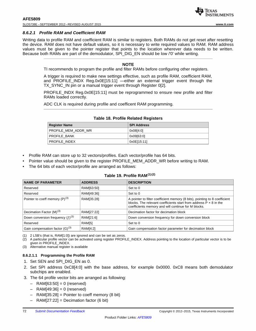
AFE5809SLOS738E –SEPTEMBER 2012–REVISED AUGUST 2015 www.ti.com
8.6.2.1 Profile RAM and Coefficient RAMWriting data to profile RAM and coefficient RAM is similar to registers. Both RAMs do not get reset after resettingthe device. RAM does not have default values, so it is necessary to write required values to RAM. RAM addressvalues must be given to the pointer register that points to the location wherever data needs to be written.Because both RAMs are part of the demodulator, SPI_DIG_EN should be low /'0' while writing.
NOTETI recommends to program the profile and filter RAMs before configuring other registers.
A trigger is required to make new settings effective, such as profile RAM, coefficient RAM,and PROFILE_INDX Reg.0x0E[15:11] —either an external trigger event through theTX_SYNC_IN pin or a manual trigger event through Register 0[2].
PROFILE_INDX Reg.0x0E[15:11] must be reprogrammed to ensure new profile and filterRAMs loaded correctly.
ADC CLK is required during profile and coefficent RAM programming.
Table 18. Profile Related RegistersRegister Name SPI AddressPROFILE_MEM_ADDR_WR 0x08[4:0]PROFILE_BANK 0x09[63:0]PROFILE_INDEX 0x0E[15:11]
spacer• Profile RAM can store up to 32 vectors/profiles. Each vector/profile has 64 bits.• Pointer value should be given to the register PROFILE_MEM_ADDR_WR before writing to RAM.• The 64 bits of each vector/profile are arranged as follows:
Table 19. Profile RAM (1) (2)
NAME OF PARAMETER ADDRESS DESCRIPTIONReserved RAM[63:50] Set to 0Reserved RAM[49:36] Set to 0Pointer to coeff memory (P) (3) RAM[35:28] A pointer to filter coefficient memory (8 bits), pointing to 8 coefficient
blocks. The relevant coefficients start from address P × 8 in thecoefficients memory and will continue for M blocks.
Decimation Factor (M) (3) RAM[27:22] Decimation factor for decimation blockDown conversion frequency (ƒ) (3) RAM[21:6] Down conversion frequency for down conversion blockReserved RAM[5] Set to 0Gain compensation factor (G) (3) RAM[4:2] Gain compensation factor parameter for decimation block
(1) 2 LSB’s (that is, RAM[1:0]) are ignored and can be set as zeros.(2) A particular profile vector can be activated using register PROFILE_INDEX. Address pointing to the location of particular vector is to be
given in PROFILE_INDEX.(3) Alternative manual register is available
8.6.2.1.1 Programming the Profile RAM1. Set SEN and SPI_DIG_EN as 0.2. Set SPI address 0xC8[4:0] with the base address, for example 0x0000. 0xC8 means both demodulator
subchips are enabled.3. The 64 profile vector bits are arranged as following:
– RAM[63:50] = 0 (reserved)– RAM[49:36] = 0 (reserved)– RAM[35:28] = Pointer to coeff memory (8 bit)– RAM[27:22] = Decimation factor (6 bit)
72 Submit Documentation Feedback Copyright © 2012–2015, Texas Instruments Incorporated
Product Folder Links: AFE5809

AFE5809www.ti.com SLOS738E –SEPTEMBER 2012–REVISED AUGUST 2015
– RAM[21:6] = Demodulation frequency (16 bit)– RAM[5] = 0– RAM[4:2] = Gain compensation factor (3 bit)– RAM[1:0] = 2 LSBs are ignored, can be set as zeros.
4. Write the above 64 bits to SPI address 0xC9 (MSB first).5. Repeat steps 3 and 4 for the following profile entries (the address in register 0xC8 auto increments).6. Set SEN and SPI_DIG_EN as 1.
8.6.2.1.2 Procedure for Configuring Next Profile Vector1. Write profile index (5 bits) to SPI address 0xCE[15:11]. 0xCE means both demodulator subchips are
enabled.
Table 20. Coefficient RAMRegister Name SPI AddressCOEFF_MEM_ADDR_WR 0x06[7:0]COEFF_BANK 0x07[111:0]MANUAL_COEFF_START_ADDR 0x1F[14:7]MANUAL_COEFF_START_EN 0x1F[15]
spacer• Coefficient RAM can store up to 256 coefficient memory blocks. The size of each block is 112 bits.• Pointer value should be given to the register COEFF_MEM_ADDR_WR before writing to RAM.• Write 112 bits to SPI address 0xC7 (MSB first). Each coefficient memory block consists of eight 14-bit
coefficients which are aligned in the following manner: coefficient order from right to left and bit order fromright to left).
Table 21. Coefficient RAM MappingCoeff 7[13:0] Coeff 6[13:0] Coeff 5[13:0] Coeff 4[13:0] Coeff 3[13:0] Coeff 2[13:0] Coeff 1[13:0] Coeff 0[13:0]
111:98 97:84 83:70 69:56 55:42 41:28 27:14 13:0
NOTEThe coefficients are in 2's complement format. SPI serialization is done from left to right(0xCoeff 7[13] first and 0xCoeff 0[0] last)
spacer• Because the decimation block uses 16 × M tap FIR filter and filter coefficients are symmetric, only half (that is
8 × M) filter coefficients are necessary to be stored (M is the decimation factor). Each 8 coefficient block thatis written to the memory represents a single phase of a polyphase filter. Therefore, the relation between thefilter coefficients Cn and their index (i,j) in the coefficients memory is given by:
n = M × (1 + I) − (1 + j)
where• I is the index in the coefficients block, from 0 to 7.• j is the block index, from 0 to (M – 1). (6)
Example for M = 4
Table 22. Coefficient RAM Mappingj\I 7 6 5 4 3 2 1 00 Coeff 31 Coeff 27 Coeff 23 Coeff 19 Coeff 15 Coeff 11 Coeff 7 Coeff 31 Coeff 30 Coeff 26 Coeff 22 Coeff 18 Coeff 14 Coeff 10 Coeff 6 Coeff 22 Coeff 29 Coeff 25 Coeff 21 Coeff 17 Coeff 13 Coeff 9 Coeff 5 Coeff 13 Coeff 28 Coeff 24 Coeff 20 Coeff 16 Coeff 12 Coeff 8 Coeff 4 Coeff 0
Copyright © 2012–2015, Texas Instruments Incorporated Submit Documentation Feedback 73
Product Folder Links: AFE5809

AFE5809SLOS738E –SEPTEMBER 2012–REVISED AUGUST 2015 www.ti.com
spacer• Coefficient start address can be given using the Pointer to Coeff Memory (P) parameter of profile RAM.
Alternatively, the start address can be given using register MANUAL_COEFF_START_ADDR. (While usingthis register, register enable bit MANUAL_COEFF_START_EN should be set to 1.)
8.6.2.1.3 Programming the Coefficient RAM1. Set SPI address 0xC6[7:0] with the base address, for example 0x0000. 0xC6 means both demodulator
subchips are enabled.2. Write 112 bits to SPI address 0xC7 (MSB first). Each coefficient memory word consists of eight 14-bit
coefficients, which are aligned in the following manner: coefficient order from right to left and bit order fromright to left.
NOTEThe coefficients are in 2s complement format.
Figure 90.
Coeff 7[13:0] Coeff 6[13:0] Coeff 5[13:0] Coeff 4[13:0] Coeff 3[13:0] Coeff 2[13:0] Coeff 1[13:0] Coeff 0[13:0]111:98 97:84 83:70 69:56 55:42 41:28 27:14 13:0
NOTESPI serialization is done from left to right (Coeff 7[13] first and Coeff 0[0] last).
3. Repeat the previous step for the following coefficient bulk entries (the address in register 0xC6 autoincrements).
8.6.2.1.4 Filter Coefficent Test Mode
Coefficient test mode allows for the streaming of coefficients through the demodulator to the LVDS. Filtercoefficient test mode can be set by the following:1. Enable TM_COEFF_EN.2. Write OUTPUT_RESOLUTION (0x03[11:9]) = 0b100, that is, 16-bit output. (output bit resolution of 14 bits will
not give proper result.)3. Write DC_REMOVAL_BYPASS (0x0A[0]) = 1, DWN_CNV_BYPASS (0x0A[2]) = 1.4. Write DC_DEC_SHIFT_FORCE_EN (0x1D[7]) = 1, DEC_SHIFT_FORCE (0x1D[6:4] = 0b110, and
DEC_SHIFT_SCALE (0x0a[13]) = 1.5. Write MODULATE_BYPASS (0x0A[14]) = 1. After writing all of the above settings, coefficients come at the
output in the sequence as follow.6. M = 2
– Address 0: C15 C13 C11 C09 C07 C05 C03 C01; Address 1: C14 C12 C10 C08 C06 C04 C02 C00– The order in which coefficients come at the output will be: 0 C01 C03 C05 C07 C09 C11 C13 C15 C14
C12 C10 C08 C06 C04 C02 C00 C00 C02 C04 C06 C08 C10 C12 C14 C15 C13 C11 C09 C07 C05 C03C01 0
7. M = 8– The coefficients come to the output as shown in Figure 91.
74 Submit Documentation Feedback Copyright © 2012–2015, Texas Instruments Incorporated
Product Folder Links: AFE5809

0 Coeff63 Coeff55 Coeff47 Coeff39 Coeff31 Coeff23 Coeff15 Coeff7
1 Coeff62 Coeff54 Coeff46 Coeff38 Coeff30 Coeff22 Coeff14 Coeff6
2 Coeff61 Coeff53 Coeff45 Coeff37 Coeff29 Coeff21 Coeff13 Coeff5
3 Coeff60 Coeff52 Coeff44 Coeff36 Coeff28 Coeff20 Coeff12 Coeff4
4 Coeff59 Coeff51 Coeff43 Coeff35 Coeff27 Coeff19 Coeff11 Coeff3
5 Coeff58 Coeff50 Coeff42 Coeff34 Coeff26 Coeff18 Coeff10 Coeff2
6 Coeff57 Coeff49 Coeff41 Coeff33 Coeff25 Coeff17 Coeff9 Coeff1
7 Coeff56 Coeff48 Coeff40 Coeff32 Coeff24 Coeff16 Coeff8 Coeff0
First sample
Last sample
AFE5809www.ti.com SLOS738E –SEPTEMBER 2012–REVISED AUGUST 2015
NOTE: When it reaches the last sample, it starts giving coefficients in the reverse direction until it reaches the point it started.
Figure 91. Coefficient Readout Sequence
8.6.2.1.5 TX_SYNC and SYNC_WORD Timing
As shown in Figure 92, hardware TX_SYNC is latched at the next negative edge of the ADC Clock after 0 to 1transition of TX_SYNC. The time gap between latched edge and the start of the LVDS SYNC_WORD is kT nswhere T is the time period of ADC clock and k = 16 + decFactor + 1. tSETUP and tHOLD can be considered as 1.5ns in the normal condition. Both are at the negative edge of the ADC clock.
Figure 92. Sync Word Generation With Respect to TX_TRIG when DC_REMOVAL_BYPASS 10[0] = 0
Copyright © 2012–2015, Texas Instruments Incorporated Submit Documentation Feedback 75
Product Folder Links: AFE5809
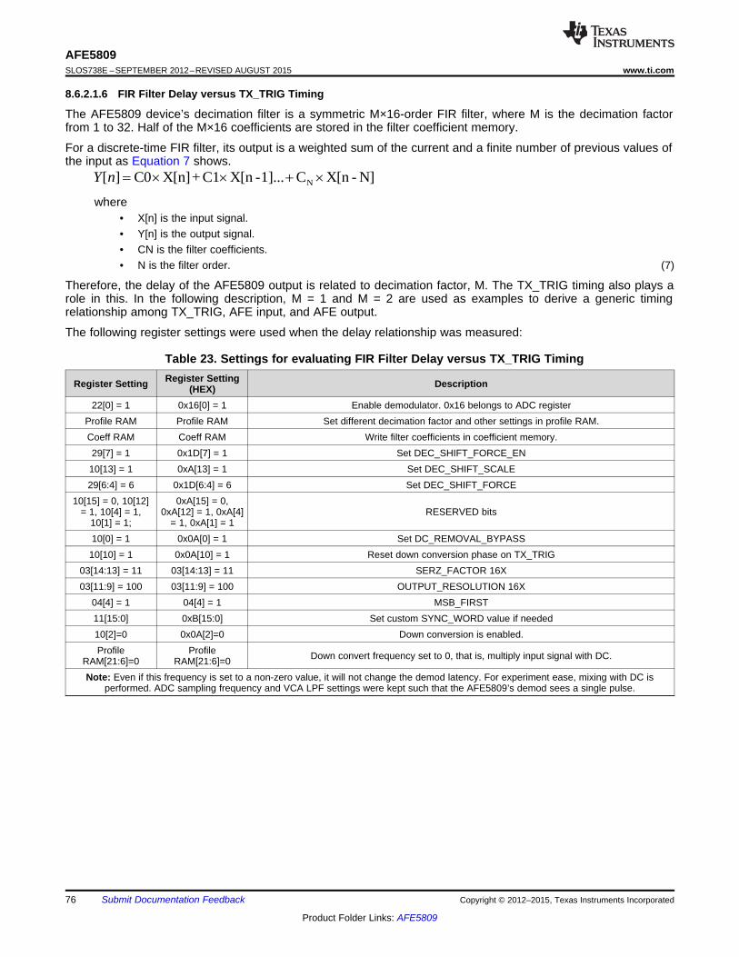
N]-X[nC1]...-X[nC1+X[n]C0][ N uuu nY
AFE5809SLOS738E –SEPTEMBER 2012–REVISED AUGUST 2015 www.ti.com
8.6.2.1.6 FIR Filter Delay versus TX_TRIG Timing
The AFE5809 device’s decimation filter is a symmetric M×16-order FIR filter, where M is the decimation factorfrom 1 to 32. Half of the M×16 coefficients are stored in the filter coefficient memory.
For a discrete-time FIR filter, its output is a weighted sum of the current and a finite number of previous values ofthe input as Equation 7 shows.
where• X[n] is the input signal.• Y[n] is the output signal.• CN is the filter coefficients.• N is the filter order. (7)
Therefore, the delay of the AFE5809 output is related to decimation factor, M. The TX_TRIG timing also plays arole in this. In the following description, M = 1 and M = 2 are used as examples to derive a generic timingrelationship among TX_TRIG, AFE input, and AFE output.
The following register settings were used when the delay relationship was measured:
Table 23. Settings for evaluating FIR Filter Delay versus TX_TRIG TimingRegister SettingRegister Setting Description(HEX)
22[0] = 1 0x16[0] = 1 Enable demodulator. 0x16 belongs to ADC registerProfile RAM Profile RAM Set different decimation factor and other settings in profile RAM.Coeff RAM Coeff RAM Write filter coefficients in coefficient memory.29[7] = 1 0x1D[7] = 1 Set DEC_SHIFT_FORCE_EN10[13] = 1 0xA[13] = 1 Set DEC_SHIFT_SCALE29[6:4] = 6 0x1D[6:4] = 6 Set DEC_SHIFT_FORCE
10[15] = 0, 10[12] 0xA[15] = 0,= 1, 10[4] = 1, 0xA[12] = 1, 0xA[4] RESERVED bits
10[1] = 1; = 1, 0xA[1] = 110[0] = 1 0x0A[0] = 1 Set DC_REMOVAL_BYPASS10[10] = 1 0x0A[10] = 1 Reset down conversion phase on TX_TRIG
03[14:13] = 11 03[14:13] = 11 SERZ_FACTOR 16X03[11:9] = 100 03[11:9] = 100 OUTPUT_RESOLUTION 16X
04[4] = 1 04[4] = 1 MSB_FIRST11[15:0] 0xB[15:0] Set custom SYNC_WORD value if needed10[2]=0 0x0A[2]=0 Down conversion is enabled.Profile Profile Down convert frequency set to 0, that is, multiply input signal with DC.RAM[21:6]=0 RAM[21:6]=0
Note: Even if this frequency is set to a non-zero value, it will not change the demod latency. For experiment ease, mixing with DC isperformed. ADC sampling frequency and VCA LPF settings were kept such that the AFE5809’s demod sees a single pulse.
76 Submit Documentation Feedback Copyright © 2012–2015, Texas Instruments Incorporated
Product Folder Links: AFE5809

ADC CLOCK
AFE INPUT
TX_TRIG
Sampling Cycle
DATA
N
DATA
N+1
DATA
N+2
DATA
N+3
DATA
N+150000 0000
Sync
WordC0 C2 C4 C6
19 Cycles
C8 C10
1 Cycles
0000
ADC CLOCK
AFE INPUT
TX_TRIG
Sampling Cycle
DATA
N
DATA
N+1
DATA
N+2
DATA
N+3
DATA
N+140000 0000
Sync
WordC0 C1 C2 C3
18 Cycles
C4 C5
2 Cycles
ADC CLOCK
AFE INPUT
TX_TRIG
Sampling Cycle
DATA
N
DATA
N+1
DATA
N+2
DATA
N+3
DATA
N+140000 0000
Sync
WordC0 C1 C2 C3
20 Cycles
AFE5809www.ti.com SLOS738E –SEPTEMBER 2012–REVISED AUGUST 2015
When M = 1, 8 filter coefficients written in the memory are C0, C1 to C7. An impulse signal is applied at bothVCA input and TX_TRIG. Due to the impulse input, coefficients start coming at the output according to timingdiagram shown in Figure 93, where 20-cycle delay is observed.
Figure 93. Expected Latency Timing When M = 1
By adjusting the timing between AFE input and TX_TRIG, the user can obtain a timing diagram similar toFigure 93.
Figure 94. Measured Latency Timing When M = 1
By adjusting the timing between AFE input and TX_TRIG, the user can obtain a timing diagram similar toFigure 94.
When M = 2, if the impulse is given one clock before TX_TRIG signal, then the demod output after sync wordgives impulse response of the filter as shown in Figure 95.
Figure 95. Measured Latency Timing When M = 2
Copyright © 2012–2015, Texas Instruments Incorporated Submit Documentation Feedback 77
Product Folder Links: AFE5809

ADC CLOCK
AFE INPUT
TX_TRIG
Sampling Cycle
DATA
N
DATA
N+1
DATA
N+2
DATA
N+3
DATA
N+140000
Sync
Word
C0 C(0+M)
C(0+2*M)
L Cycles
C(0+3*M)NOz
S Cycles
IP Cycles 20 Cycles
AFE5809SLOS738E –SEPTEMBER 2012–REVISED AUGUST 2015 www.ti.com
Figure 96 shows a generic timing diagram. The number of zeros comes before the sync word is equal to Z. Thesync word comes after S number of cycles, impulse response starts coming after L number of cycles, and inputimpulse is given after IP cycles with respect to TX_TRIG signal. Therefore, for different decimation factor (M),values of these numbers are listed in Table 24 and Figure 96.
Table 24. Generic Latency versus Decimation Factor M (1) (2)
M Number of Zeros (ZNo) Sync Word Latency (S) Data Latency (L) Input Impulse (IP) (3)
1 2 17 18 –22 3 18 19 –13 4 19 20 04 5 20 21 15 6 21 22 26 7 22 23 37 8 23 24 48 9 24 25 5M M + 1 16 + M 17 + M M – 3
(1) When DC_REMOVAL_BYPASS 10[0] = 0 or 0xA[0] = 0, the sync word latency and data latency becomes 17 + M and 18 + M(2) ADC's low latency mode enabled by register 0x2[12] does not impact S and L.(3) Negative number represents input is given in advance with respect to TX_TRIG signal.
Figure 96. Measured Latency Timing at Any M
8.6.2.1.6.0.1 Expression of Decimation Filter Response
Based on Table 24, the decimation filter’s response is formulated. Figure 97 indicates that the Tx_Trig sample isconsidered as the reference for time scale. So, the input to the device at Tx_Trig clock will be expressed as X[0],the next sample input as X[1], and so on. Similarly, the output of the device followed by the AFE5809’sdemodulator will be expressed as Y[0] at the instant of Tx_Trig, Y[1] at the next clock, and so on; Cn or C(n)indicates the coefficient of nth index.
78 Submit Documentation Feedback Copyright © 2012–2015, Texas Instruments Incorporated
Product Folder Links: AFE5809

ADC CLOCK
INPUT
TX_TRIG
Y[0] 0000Sync
Word
X[0]X[-1]X[-2] X[1] X[2] X[3] X[4] X[14] X[15]
Y[1] Y[2] Y[3] Y[14] Y[15]=Y[17+M]
X[17+M]
AFE5809www.ti.com SLOS738E –SEPTEMBER 2012–REVISED AUGUST 2015
Figure 97. Typical Timing Expression Among ADC CLK, Input, TX_TRIG, and Output
For M = 1, the number of zeros, ZNo = 2; Sync word latency S = 17. So, the output values from sample 18 arerelevant and the first few samples are:
Y[18] = C0×X[-2]+C1×X[-3]+C2×X[-4]+…+C7×X[-9]+C7×X[-10]+…+C[0]×X[-17]
Y[19] = C0×X[-1]+C1×X[-2]+C2×X[-3]+…+C7×X[-8]+C7×X[-9]+…+C[0]×X[-16]
Y[20] = C0×X[0]+C1×X[-1]+C2×X[-2]+…+C7×X[-7]+C7×X[-8]+…+C[0]×X[-15](8)
All these samples appear at the output because no samples are dropped for decimation factor = 1.
For M = 2, the number of zeros, ZNo = 3; Sync word latency S = 18. So, the output values from sample 19 arerelevant and the first few samples are described as:
Y[19] = C0×X[-1]+C1×X[-2]+C2×X[-3]+…+C15×X[-16]+C15×X[-17]+…+C[0]×X[-32]
Y[20] = C0×X[0]+C1×X[-1]+C2×X[-2]+…+C15×X[-15]+C15×X[-16]+…+C[0]×X[-31]
Y[21] = C0×X[1]+C1×X[0]+C2×X[-1]+…+C15×X[-14]+C15×X[-15]+…+C[0]×X[-30](9)
But for M = 2, every alternate sample must be dropped. The decimation is adjusted in such a way that the firstsample after sync is retained. Hence in this case, Y[19], Y[21], Y[23], and so forth are retained and Y[20], Y[22],Y[24], and so forth are dropped.
For M = 3, the number of zeros, ZNo = 4; Sync word latency S = 19. So, the output values from sample 20 arerelevant and the first few samples are described as:
Y[20] = C0×X[0]+C1×X[-1]+C2×X[-2]+…+C23×X[-23]+C23×X[-24]+…+C[0]×X[-47]
Y[21] = C0×X[1]+C1×X[0]+C2×X[-1]+…+C23×X[-22]+C23×X[-23]+…+C[0]×X[-46]
Y[22] = C0×X[2]+C1×X[1]+C2×X[0]+…+C23×X[-21]+C23×X[-22]+…+C[0]×X[-45]
Y[23] = C0×X[3]+C1×X[2]+C2×X[1]+…+C23×X[-20]+C23×X[-21]+…+C[0]×X[-44]
(10)
But for M = 3, the last two of every three samples must be dropped. The decimation is adjusted in such a waythat the first sample after sync is retained. Hence in this case, Y[20], Y[23], Y[26], and so forth are retained andY[21], Y[22], Y[24], Y[25], and so forth are dropped.
For any M, this pattern can be generalized for a decimation factor of M. The number of ZNo = M + 1, Sync wordlatency S = 16 + M. So, the output values from sample (17 + M) are relevant and the first few samples aredescribed as:
Y[17+M] = C0×X[M-3]+C1×X[M-4]+C2×X[M-5]+…+C(8M-1)×X[-7M-2]+C(8M-1)×X[-7M-3]+ … +C[0]×X[-15M-2]
Y[18+M] = C0×X[M-2]+C1×X[M-3]+C2×X[M-4]+…+C(8M-1)×X[-7M-1]+C(8M-1)×X[-7M-2]+ … +C[0]×X[-15M-1](11)
Copyright © 2012–2015, Texas Instruments Incorporated Submit Documentation Feedback 79
Product Folder Links: AFE5809

AFE5809SLOS738E –SEPTEMBER 2012–REVISED AUGUST 2015 www.ti.com
For a decimation factor of M which is not 1, the decimation is adjusted in such a way that the first sample aftersync is retained. Hence in this case, Y[17 + M], Y[17 + 2M], Y[17 + 3M], and so forth are retained and the rest ofsamples between these, that is, Y[18 + M], Y[19 + 2M],…, Y[16 + 2M] are dropped.
80 Submit Documentation Feedback Copyright © 2012–2015, Texas Instruments Incorporated
Product Folder Links: AFE5809

AFE5809www.ti.com SLOS738E –SEPTEMBER 2012–REVISED AUGUST 2015
9 Application and Implementation
NOTEInformation in the following applications sections is not part of the TI componentspecification, and TI does not warrant its accuracy or completeness. TI’s customers areresponsible for determining suitability of components for their purposes. Customers shouldvalidate and test their design implementation to confirm system functionality.
9.1 Application Information
Figure 98 lists a typical application circuit diagram. The configuration for each block is discussed in the followingsections. lists companion TI devices to complete the analog signal chain in a system.
Table 25. Application Companion DevicesPart Number Part Description Functions
THS4130, SLOS318 Fully Differential Input/Output Low Noise Amplifier With Shutdown TGC Vcntl Opamp, CW summing amplifier and active filter
TGC Vcntl amplifier, CW summing amplifier and activeOPA1632, SBOS286 Fully Differential I/O Audio Amplifier filter
OPA2211A, SBOS377 1.1nV/rtHz Noise, Low Power, Precision Operational Amplifier CW summing amplifier and active filter
LME49990, SNOSB16 Ultra-low Distortion, Ultra-low Noise Operational Amplifier CW summing amplifier and active filter
LMH6629, SNOSB18 Ultra-Low Noise, High-Speed Operational Amplifier with Shutdown CW summing amplifier and active filter
16-bit, Unipolar Diff Input, 2MSPS Sampling rate, 4.75V to 5.25VADS8413, SLAS490 CW Audio ADCADC with LVDS Serial Interface
18-Bit, 1-MSPS, Serial Interface, microPower, Truly-Differential Input,ADS8881, SBAS547 CW Audio ADCSAR ADC
DAC7811, SBAS337 12-Bit, Serial Input, Multiplying Digital to Analog Converter TGC Vcntl Digital to Analog Converter
Low Noise Clock Jitter Cleaner With Dual Cascaded PLLs andLMK04803, SNAS489 Jitter cleaner and clock synthesizerIntegrated 1.9 GHz VCO
CDCM7005, SCAS793 High Performance, Low Phase Noise, Low Skew Clock Synchronizer Jitter cleaner and clock synthesizer
CDCE72010, SLAS490 10 Outputs Low Jitter Clock Synchronizer and Jitter Cleaner Jitter cleaner and clock synthesizer
CDCLVP1208, SCAS890 Low Jitter, 2-Input Selectable 1:8 Universal-to-LVPECL Buffer Clock buffer
LMK00308, SNAS576 3.1-GHz Differential Clock Buffer/Level Translator Clock buffer
LMK01000, SNAS437 1.6 GHz High Performance Clock Buffer, Divider, and Distributor Clock buffer
Low Power, 1.8/2.5/3.3-V Input, 3.3-V CMOS Output, Single InverterSN74AUP1T04, SCES800 1.8V/2.5V/3.3V Level shifter for SPIGate
UCC28250, SLUSA29 Advanced PWM Controller with Prebias Operation Synchronized DC-DC power supply controller
Copyright © 2012–2015, Texas Instruments Incorporated Submit Documentation Feedback 81
Product Folder Links: AFE5809

IN CH1
IN CH2
IN CH3
IN CH4
IN CH5
IN CH6
IN CH7
IN CH8
ACT1
ACT2
ACT3
ACT4
ACT5
ACT6
ACT7
ACT8
IN1P
IN2P
IN3P
IN4P
IN5P
IN6P
IN7P
IN8P
IN1M
IN2M
IN3M
IN4M
IN5M
IN6M
IN7M
IN8M
AFE5809
ANALOG INPUTSANALOG OUTPUTS
REF/BIAS DECOUPLINGLVDS OUTPUTS
D1P
D1M
D2P
D2M
D3P
D3M
D4P
D4M
D5P
D5M
D6P
D6M
D7P
D7M
D8P
D8M
DCLKM
DCLKP
FCLKM
FCLKP
CW_IP_AMPINP
CW_IP_AMPINM
CW_IP_OUTM
CW_IP_OUTP
REFM
REFP
CLKM
CLKP
AFE5809
CLOCKINPUTS
AFE5809
DIGITALINPUTS
CLKM_16X
CLKP_16X
CLKM_1X
CLKP_1X
0.1μF
0.1μF
0.1μF
0.1μF
0.1μF
0.1μF
SCLK
SDATA
RESET
SEN
SOUT
PDN_ADC
PDN_VCA
PDN_GLOBAL
AVSS DVSS
AVSS AVSS AVSS DVSS
OTHERAFE5809OUTPUT
OTHERAFE5809OUTPUT
OTHERAFE5809OUTPUT
DNCs
TOSUMMING
AMP
CAC
CCW
CCW
CAC
CAC
CAC
RSUM
CVCNTL
470pF
CVCNTL
470pF
REXT (optional)
REXT (optional) RSUM
RSUM
RSUM
CW_QP_AMPINP
CW_QP_AMPINM
CW_QP_OUTM
CW_QP_OUTP
OTHERAFE5809OUTPUT
TOSUMMING
AMP
CAC
CCW
CCW
CAC
CAC
CAC
RSUM
REXT (optional)
REXT (optional)
RSUM
RSUM
RSUM
Clock terminationdepends on clock typesLVDS, PECL, or CMOS
5VA
AV
DD
_5
V
AV
DD
_A
DC
AV
DD
DV
DD
3.3VA 1.8VA 1.8VD10μF
1μF
1μF
1μF
1μF
1μF
1μF
1μF
1μF
>1μF
>1μF
0.1μF
0.1μF
0.1μF
0.1μF
0.1μF
0.1μF
0.1μF
0.1μF
0.1μF
15nF
15nF
15nF
15nF
15nF
15nF
15nF
15nF
10μF 10μF 10μF
0.1μF N*0.1 Fμ N*0.1 Fμ N*0.1 Fμ
CM_BYP
VHIGH
VCNTLP INVCNTLP
VCNTLM
VREF_IN
RVCNTL
200Ω
RVCNTL
200Ω
VCNTLM IN
1.4V
TX_SYNC_IN
SPI_DIG_EN
AFE5809
DigitalI/Q
Demod
LDO_SETV
LDO_EN
DVDD_LDO1
0.1μF
0.1μF
DVDD_LDO2
Logic ‘1’: 1.8V
Logic ‘1’: 1.8V
AFE5809SLOS738E –SEPTEMBER 2012–REVISED AUGUST 2015 www.ti.com
9.2 Typical Application
Figure 98. Application Circuit With Digital Demodulator
82 Submit Documentation Feedback Copyright © 2012–2015, Texas Instruments Incorporated
Product Folder Links: AFE5809

AFE5809www.ti.com SLOS738E –SEPTEMBER 2012–REVISED AUGUST 2015
Typical Application (continued)9.2.1 Design RequirementsThe AFE5809 device is a highly integrated analog front-end solution. To maximize its performance, users mustcarefully optimize its surrounding circuits, such as T/R switch, Vcntl circuits, audio ADCs for CW path, clockdistribution network, synchronized power supplies and digital processors. Typical requirements for a traditionalmedical ultrasound imaging system are shown in Table 26.
Table 26. Design ParametersPARAMETER EXAMPLE VALUES
Signal center frequency (f0) 1~20 MHzSignal Bandwidth (BW) 10~100% of f0
Overloaded signals due to T/R ~2 Vppswitch leakageMaximum input signal amplitude 100 mVpp to 1 Vpp
Transducer noise level 1 nV/rtHzDynamic range 151 dBc/Hz
Time gain compensation range 40 dBTotal harmonic distortion 40 dBc at 5MHz
9.2.2 Detailed Design ProcedureMedical ultrasound imaging is a widely-used diagnostic technique that enables visualization of internal organs,their size, structure, and blood flow estimation. An ultrasound system uses a focal imaging technique thatinvolves time shifting, scaling, and intelligently summing the echo energy using an array of transducers toachieve high imaging performance. The concept of focal imaging provides the ability to focus on a single point inthe scan region. By subsequently focusing at different points, an image is assembled.
When initiating an imaging, a pulse is generated and transmitted from each of the 64 transducer elements. Thepulse, now in the form of mechanical energy, propagates through the body as sound waves, typically in thefrequency range of 1MHz to 15 MHz. The sound waves are attenuated as they travel through the objects beingimaged, and the attenuation coefficients ɑ are about 0.54 dB/(MHz×cm) in soft tissue and 6~10 dB/(MHz×cm) inbone as shown in many published papers. Most medical ultrasound systems use the reflection imaging modeand the total signal attenuation is calculated by 2×depth×ɑ×f0. As the signal travels, portions of the wave frontenergy are reflected. Signals that are reflected immediately after transmission are very strong because they arefrom reflections close to the surface; reflections that occur long after the transmit pulse are very weak becausethey are reflecting from deep in the body. As a result of the limitations on the amount of energy that can be putinto the imaging object, the industry developed extremely sensitive receive electronics with wide dynamic range.
Receive echoes from focal points close to the surface require little, if any, amplification. This region is referred toas the near field. However, receive echoes from focal points deep in the body are extremely weak and must beamplified by a factor of 100 or more. This region is referred to as the far field. In the high-gain (far field) mode,the limit of performance is the sum of all noise sources in the receive chain. In high-gain (far field) mode, systemperformance is defined by its overall noise level, which is limited by the noise level of the transducer assemblyand the receive low-noise amplifier (LNA). However in the low-gain (near field) mode, system performance isdefined by the maximum amplitude of the input signal that the system can handle. The ratio between noise levelsin high-gain mode and the signal amplitude level in low-gain mode is defined as the dynamic range of thesystem. The high integration and high dynamic range of the device make it ideally suited for ultrasound imagingapplications.
The device includes an integrated LNA and VCAT (which use the gain that can be changed with enough time tohandle both near- and far-field systems), a low-pass anti-aliasing filter to limit the noise bandwidth, an ADC withhigh SNR performance, and a CW mixer.
Use the following steps to design medical ultrasound imaging systems:1. Use the signal center frequency and signal bandwidth to select an appropriate ADC sampling frequency.2. Use the time gain compensation range to select the range of the VCNTL signal.3. Use the transducer noise level and maximum input signal amplitude to select the appropriate LNA gain. The
device input-referred noise level reduces with higher LNA gain. However, higher LNA gain leads to lower
Copyright © 2012–2015, Texas Instruments Incorporated Submit Documentation Feedback 83
Product Folder Links: AFE5809

S0498-01
CLAMP
AFE
LNAx
DC OffsetCorrection
ACTx
CACT
CIN
CBYPASS
INPx
INMx
Input
OptionalDiodes
AFE5809SLOS738E –SEPTEMBER 2012–REVISED AUGUST 2015 www.ti.com
input signal swing support.4. Select different passive components for different device pins.5. Select the appropriate input termination configuration.6. Select the clock configuration for the ADC and CW clocks
9.2.2.1 LNA Configuration
9.2.2.1.1 LNA Input Coupling and Decoupling
The LNA closed-loop architecture is internally compensated for maximum stability without the need of externalcompensation components. The LNA inputs are biased at 2.4 V and AC coupling is required. Figure 99 shows atypical input configuration. CIN is the input AC coupling capacitor. CACT is a part of the active terminationfeedback path. Even if the active termination is not used, the CACT is required for the clamp functionality. Therecommended values for CACT is ≥1 µF and CIN is ≥0.1 µF. A pair of clamping diodes is commonly placedbetween the T/R switch and the LNA input. Schottky diodes with suitable forward drop voltage (for example: theBAT754/54 series, the BAS40 series, the MMBD7000 series, or similar) can be considered depending on thetransducer echo amplitude.
Figure 99. LNA Input Configurations
This architecture minimizes any loading of the signal source that may lead to a frequency-dependent voltagedivider. The closed-loop design yields low offsets and offset drift. CBYPASS (≥0.015 µF) is used to set the HPF cut-off frequency and decouple the complementary input. Its cut-off frequency is inversely proportional to the CBYPASSvalue. The HPF cut-off frequency can be adjusted through the register 59[3:2] Table 27 lists. Low-frequencysignals at T/R switch output, such as signals with slow ringing, can be filtered out. In addition, the HPF canminimize system noise from DC-DC converters, pulse repetition frequency (PRF) trigger, and frame clock. Mostultrasound systems’ signal-processing unit includes digital HPFs or band-pass filters (BPFs) in FPGAs or ASICs.Further noise suppression can be achieved in these blocks. In addition, a digital HPF is available in the AFE5809ADC. If low-frequency signal detection is desired in some applications, the LNA HPF can be disabled.
Table 27. LNA HPF Settings (CBYPASS = 15 nF)Reg59[3:2] (0x3B[3:2]) FREQUENCY (kHz)
00 10001 5010 20011 150
84 Submit Documentation Feedback Copyright © 2012–2015, Texas Instruments Incorporated
Product Folder Links: AFE5809

(b) Active Termination
S0499-01
LNARs
(a) No Termination
(c) Passive Termination
LNARs
Rf
LNARs Rt
2 2 2
total LNAnoise s LNAnoiseLNA _Noise V R I= + ´
AFE5809www.ti.com SLOS738E –SEPTEMBER 2012–REVISED AUGUST 2015
CM_BYP and VHIGH pins, which generate internal reference voltages, must be decoupled with ≥1-µF capacitors.Bigger bypassing capacitors (>2.2 µF) may be beneficial if low-frequency noise exists in the system.
9.2.2.1.2 LNA Noise Contribution
The noise specification is critical for LNA and it determines the dynamic range of the entire system. The LNA ofthe AFE5809 device achieves low power and an exceptionally low-noise voltage of 0.63 nV/√Hz, and a lowcurrent noise of 2.7 pA/√Hz.
Typical ultrasonic transducer’s impedance, RS, varies from tens of Ω to several hundreds of Ω. Voltage noise isthe dominant noise in most cases; however, the LNA current noise flowing through the source impedance (RS)generates additional voltage noise.
(12)
The AFE5809 device achieves low-noise figure (NF) over a wide range of source resistances as shown inFigure 32, Figure 33, and Figure 34.
9.2.2.1.3 Active Termination
In ultrasound applications, signal reflection exists due to long cables between the transducer and system. Thereflection results in extra ringing added to echo signals in PW mode. Because the axial resolution depends onecho signal length, such ringing effect can degrade the axial resolution. Therefore, either passive termination oractive termination is preferred if good axial resolution is desired. Figure 100 shows three terminationconfigurations.
Figure 100. Termination ConfigurationsCopyright © 2012–2015, Texas Instruments Incorporated Submit Documentation Feedback 85
Product Folder Links: AFE5809

IN IN IN
LNA
RZ / /C / /R
A1
2
=n
+
f
IN
LNA
RZ
A1
2
=n
+
f
S0500-01
AFE
LNAx
ACTx
INPx
INMx
Input
4500Ω
3600Ω
1800Ω
900Ω
450Ω
AFE5809SLOS738E –SEPTEMBER 2012–REVISED AUGUST 2015 www.ti.com
Under the no termination configuration, the input impedance of the AFE5809 is about 6 kΩ (8 K//20 pF) at 1MHz. Passive termination requires external termination resistor Rt, which contributes to additional thermal noise.
The LNA supports active termination with programmable values, as shown in Figure 101 .
Figure 101. Active Termination Implementation
The AFE5809 device has four pre-settings 50, 100, 200, and 400 Ω, which are configurable through theregisters. Other termination values can be realized by setting the termination switches shown in Figure 101.Register [52] is used to enable these switches. The input impedance of the LNA under the active terminationconfiguration approximately follows:
(13)
Table 5 lists the LNA RINs under different LNA gains. System designers can achieve fine tuning for differentprobes.
The equivalent input impedance is given by Equation 14 where RIN (8 kΩ) and CIN (20 pF) are the inputresistance and capacitance of the LNA.
(14)
Therefore, the ZIN is frequency dependent, and it decreases as frequency increases as shown in Figure 10.Because 2 to 10 MHz is the most commonly used frequency range in medical ultrasound, this rolling-off effectdoes not impact system performance greatly. Active termination can be applied to both CW and TGC modes.Because each ultrasound system includes multiple transducers with different impedances, the flexibility ofimpedance configuration is a great plus.
Figure 32, Figure 33, and Figure 34 show the NF under different termination configurations. It indicates that notermination achieves the best noise figure; active termination adds less noise than passive termination. Thus,termination topology should be carefully selected based on each use scenario in ultrasound.
86 Submit Documentation Feedback Copyright © 2012–2015, Texas Instruments Incorporated
Product Folder Links: AFE5809

W0004-01
(a) Single-Ended Input at VCNTLP
(b) Differential Inputs at V and VCNTLP CNTLM
TGC Gain
V = 0VCNTLM
VCNTLP
1.5V
XdB
X+40dB
TGC Gain
0V
VCNTLM
VCNTLP
XdB
X+40dB
1.5V
0.75V
AFE5809www.ti.com SLOS738E –SEPTEMBER 2012–REVISED AUGUST 2015
9.2.2.1.4 LNA Gain Switch Response
The LNA gain is programmable through SPI. The gain switching time depends on the SPI speed as well as theLNA gain response time. During the switching, glitches might occur and they can appear as artifacts in images.In addition, the signal chain needs about 14 µs to settle after the LNA gain change. Thus, LNA gain switchingmay not be preferred when switching time or settling time for the signal chain is limited.
9.2.2.2 Voltage-Controlled AttenuatorThe attenuator in the AFE5809 device is controlled by a pair of differential control inputs, the VCNTLM,P pins. Thedifferential control voltage spans from 0 to 1.5 V. This control voltage varies the attenuation of the attenuatorbased on its linear-in-dB characteristic. Its maximum attenuation (minimum channel gain) appears at VCNTLP –VCNTLM = 1.5 V and minimum attenuation (maximum channel gain) occurs at VCNTLP – VCNTLM = 0. The typicalgain range is 40 dB and remains constant, independent of the PGA setting.
When only single-ended VCNTL signal is available, this 1.5-Vpp signal can be applied on the VCNTLP pin with theVCNTLM pin connected to ground; As Figure 102 show, the TGC gain curve is inversely proportional to theVCNTLP – VCNTLM.
Figure 102. VCNTLP and VCNTLM Configurations
Copyright © 2012–2015, Texas Instruments Incorporated Submit Documentation Feedback 87
Product Folder Links: AFE5809

Frequency (kHz)
Noi
se (
nV/
Hz)
1 2 3 4 5 7 10 20 30 50 100 200 500 1000 50000
1
2
3
4
5
6
7
8
9
10
D063
16 Channels32 Channels64 Channels128 Channels192 Channels
AFE5809SLOS738E –SEPTEMBER 2012–REVISED AUGUST 2015 www.ti.com
As discussed in the theory of operation, the attenuator architecture uses seven attenuator segments that areequally spaced to approximate the linear-in-dB gain-control slope. This approximation results in a monotonicslope; the gain ripple is typically less than ±0.5 dB.
The control voltage input (VCNTLM,P pins) represents a high-impedance input. The VCNTLM,P pins of multipleAFE5809 devices can be connected in parallel with no significant loading effects. When the voltage level(VCNTLP – VCNTLM) is above 1.5 V or below 0 V, the attenuator continues to operate at its maximum attenuationlevel or minimum attenuation level, respectively. TI recommends lmiting the voltage from –0.3 to 2 V.
When the AFE5809 device operates in CW mode, the attenuator stage remains connected to the LNA outputs.Therefore, TI recommends powering down the VCA using the PDN_VCA register bit. In this case, VCNTLP –VCNTLM voltage does not matter.
The AFE5809 gain-control input has a –3-dB bandwidth of approximately 800 kHz. This wide bandwidth,although useful in many applications (for example, fast VCNTL response), can also allow high-frequency noise tomodulate the gain control input and finally affect the Doppler performance. In practice, this modulation can beavoided by additional external filtering (RVCNTL and CVCNTL) at VCNTLM,P pins as Figure 81 shows. However, theexternal filter's cutoff frequency cannot be kept too low as this results in low gain response time. Without externalfiltering, the gain control response time is typically less than 1 μs to settle within 10% of the final signal level of1VPP (–6-dBFS) output as indicated in Figure 51 and Figure 52.
Typical VCNTLM,P signals are generated by an 8- to 12-bit 10-MSPS digital-to-analog converter (DAC) and adifferential operation amplifier. TI’s DACs, such as TLV5626 and DAC7821/11 (10 MSPS/12 bit), could be usedto generate TGC control waveforms. Differential amplifiers with output common mode voltage control (that is,THS4130 and OPA1632) can connect the DAC to the VCNTLM/P pins. The buffer amplifier can also be configuredas an active filter to suppress low-frequency noise. The VCNTLM/P circuit achieves low noise to prevent theVCNTLM/P noise being modulated to RF signals. TI recommends that VCNTLM/P noise is below 25 nV/rtHz at 1 kHzand 5 nV/rtHz at 50 kHz. In high-channel count premium systems, the VCNTLM/P noise requirement is higher. SeeFigure 103
Figure 103. Allowed Noise on the VCNTL Signal Across Frequency and Different Channels
More information can be found in SLOS318 and SBAA150. See Figure 2 for the VCNTL vs Gain curves. Table 28also shows the absolute gain vs VCNTL, which may help program DAC correspondingly.
In PW Doppler and color Doppler modes, VCNTL noise should be minimized to achieve the best close-in phasenoise and SNR. Digital VCNTL feature is implemented to address this need in the AFE5809. In the digital VCNTLmode, no external VCNTL is needed.
88 Submit Documentation Feedback Copyright © 2012–2015, Texas Instruments Incorporated
Product Folder Links: AFE5809

HP
INT/EXT EXT
1
2 R C=
p
f
AFE5809www.ti.com SLOS738E –SEPTEMBER 2012–REVISED AUGUST 2015
Table 28. VCNTLP – VCNTLM vs Gain Under Different LNA and PGA Gain Settings (Low-Noise Mode)Gain (dB) Gain (dB) Gain (dB) Gain (dB) Gain (dB) Gain (dB)VCNTLP – VCNTLM LNA = 12 dB LNA = 18 dB LNA = 24 dB LNA = 12 dB LNA = 18 dB LNA = 24 dB(V) PGA = 24 dB PGA = 24 dB PGA = 24 dB PGA = 30 dB PGA = 30 dB PGA = 30 dB
0 36.45 42.45 48.45 42.25 48.25 54.250.1 33.91 39.91 45.91 39.71 45.71 51.710.2 30.78 36.78 42.78 36.58 42.58 48.580.3 27.39 33.39 39.39 33.19 39.19 45.190.4 23.74 29.74 35.74 29.54 35.54 41.540.5 20.69 26.69 32.69 26.49 32.49 38.490.6 17.11 23.11 29.11 22.91 28.91 34.910.7 13.54 19.54 25.54 19.34 25.34 31.340.8 10.27 16.27 22.27 16.07 22.07 28.070.9 6.48 12.48 18.48 12.28 18.28 24.281 3.16 9.16 15.16 8.96 14.96 20.96
1.1 –0.35 5.65 11.65 5.45 11.45 17.451.2 –2.48 3.52 9.52 3.32 9.32 15.321.3 –3.58 2.42 8.42 2.22 8.22 14.221.4 –4.01 1.99 7.99 1.79 7.79 13.791.5 –4 2 8 1.8 7.8 13.8
9.2.2.3 CW Operation
9.2.2.3.1 CW Summing Amplifier
To simplify CW system design, a summing amplifier is implemented in the AFE5809 to sum and convert 8-channel mixer current outputs to a differential voltage output. Low noise and low power are achieved in thesumming amplifier while maintaining the full dynamic range required in CW operation.
This summing amplifier has five internal gain adjustment resistors which can provide 32 different gain settings(register 54[4:0], Figure 101 and Table 8). System designers can easily adjust the CW path gain depending onsignal strength and transducer sensitivity. For any other gain values, an external resistor option is supported. Thegain of the summation amplifier is determined by the ratio between the 500-Ω resistors after LNA and the internalor external resistor network REXT/INT. Thus, the matching between these resistors plays a more important rolethan absolute resistor values. Better than 1% matching is achieved on chip. Due to process variation, theabsolute resistor tolerance could be higher. If external resistors are used, the gain error between I/Q channels oramong multiple AFEs may increase. TI recommends using internal resistors to set the gain to achieve better gainmatching (across channels and multiple AFEs). With the external capacitor CEXT , this summing amplifier hasfirst-order LPF response to remove high-frequency components from the mixers, such as 2f0±fd. Its cut-offfrequency is determined by:
(15)
When different gain is configured through Register 54[4:0], the LPF response varies as well.
Copyright © 2012–2015, Texas Instruments Incorporated Submit Documentation Feedback 89
Product Folder Links: AFE5809

S0501-01
I/V SumAmp
CW_AMPINP CW_OUTM
CW_AMPINM CW_OUTP
CEXT
CEXT
REXT
REXT
RINT
RINT
2000Ω
2000Ω
1000Ω
1000Ω
500Ω
500Ω
250Ω
250Ω
250Ω
250Ω
AFE5809SLOS738E –SEPTEMBER 2012–REVISED AUGUST 2015 www.ti.com
Figure 104. CW Summing Amplifier Block Diagram
Multiple AFE5809 devices are usually used in parallel to expand CW beamformer channel count. The AFE5809CW's voltage outputs can be summed and filtered externally further to achieve desired gain and filter response.AC-coupling capacitors CAC are required to block the DC component of the CW carrier signal. CAC can vary from1 to 10 μF depending on the desired low-frequency Doppler signal from slow blood flow. Multiple AFE5809s’ I/Qoutputs can be summed together with a low-noise differential amplifiers before 16, 18-bit differential audio ADCs.The TI ultralow noise differential precision amplifier OPA1632 and THS4130 are suitable devices.
90 Submit Documentation Feedback Copyright © 2012–2015, Texas Instruments Incorporated
Product Folder Links: AFE5809
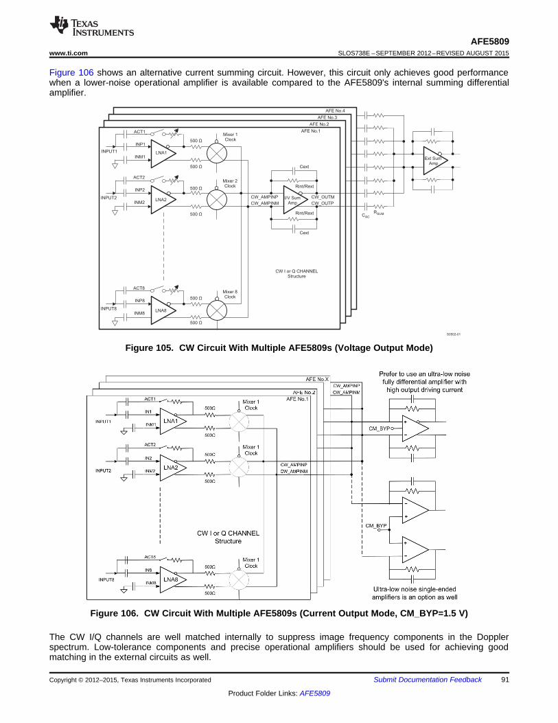
S0502-01
500 Ω
I/V SumAmp
Cext
Cext
Rint/Rext
Rint/Rext
CW_OUTM
CW_OUTP
Ext SumAmp
LNA1INM1
LNA2INM2
LNA8INM8
CW I or Q CHANNELStructure
INPUT1
INPUT2
INPUT8
AFE No.2
AFE No.3
AFE No.4
AFE No.1
CW_AMPINP
CW_AMPINM
Mixer 1Clock
Mixer 2Clock
Mixer 8Clock
ACT1
ACT2
ACT8
CAC
RSUM
INP1
INP2
INP8
500 Ω
500 Ω
500 Ω
500 Ω
500 Ω
AFE5809www.ti.com SLOS738E –SEPTEMBER 2012–REVISED AUGUST 2015
Figure 106 shows an alternative current summing circuit. However, this circuit only achieves good performancewhen a lower-noise operational amplifier is available compared to the AFE5809's internal summing differentialamplifier.
Figure 105. CW Circuit With Multiple AFE5809s (Voltage Output Mode)
Figure 106. CW Circuit With Multiple AFE5809s (Current Output Mode, CM_BYP=1.5 V)
The CW I/Q channels are well matched internally to suppress image frequency components in the Dopplerspectrum. Low-tolerance components and precise operational amplifiers should be used for achieving goodmatching in the external circuits as well.
Copyright © 2012–2015, Texas Instruments Incorporated Submit Documentation Feedback 91
Product Folder Links: AFE5809

S0503-01
(a) LVPECL Configuration
(c) Transformer Based Configuration
(d) CMOS Configuration
(b) LVDS Configuration
CMOS CLKDriver
AFECMOS CLK
CMOS
AFECLOCKs
CLOCKSOURCE
50 Ω
0.1 Fμ
0.1 Fμ
0.1 Fμ
0.1 Fμ
CDCE72010AFE
CLOCKs100 Ω
LVDS
0.1 Fμ
0.1 Fμ
CDCM7005CDCE7010
AFECLOCKs
130 Ω
LVPECL
0.1 Fμ
0.1 Fμ
83 Ω 3.3 V
3.3 V
130 Ω
AFE5809SLOS738E –SEPTEMBER 2012–REVISED AUGUST 2015 www.ti.com
NOTEThe local oscillator inputs of the passive mixer are cos(ωt) for I-CH and sin(ωt) for Q-CH,respectively. Depending on the users' CW Doppler complex FFT processing, swapping I/Qchannels in FPGA or DSP may be needed to get correct blood flow directions.
9.2.2.3.2 CW Clock Selection
The AFE5809 device can accept differential LVDS, LVPECL, and other differential clock inputs as well as single-ended CMOS clock. An internally generated VCM of 2.5 V is applied to CW clock inputs, that is, CLKP_16X/CLKM_16X and CLKP_1X/ CLKM_1X. Because this 2.5-V VCM is different from the one used in standard LVDSor LVPECL clocks, AC coupling is required between clock drivers and the AFE5809 CW clock inputs. When theCMOS clock is used, CLKM_1X and CLKM_16X should be tied to ground. Figure 107 shows common clockconfigurations. TI recommends appropriate termination to achieve good signal integrity.
Figure 107. Clock Configurations92 Submit Documentation Feedback Copyright © 2012–2015, Texas Instruments Incorporated
Product Folder Links: AFE5809

AFE5809www.ti.com SLOS738E –SEPTEMBER 2012–REVISED AUGUST 2015
The combination of the clock noise and the CW path noise can degrade the CW performance. The internalclocking circuit is designed for achieving excellent phase noise required by CW operation. The phase noise ofthe AFE5809 CW path is better than 155 dBc/Hz at 1-kHz offset. Consequently, the phase noise of the mixerclock inputs needs to be better than 155 dBc/Hz.
In the 16/8/4 × ƒcw operations modes, low phase noise clock is required for 16, 8, 4 × ƒcw clocks (that is,CLKP_16X/ CLKM_16X pins) to maintain good CW phase noise performance. The 1 × ƒcw clock (that is,CLKP_1X/ CLKM_1X pins) is only used to synchronize the multiple AFE5809 chips and is not used fordemodulation. Thus, 1 × ƒcw clock’s phase noise is not a concern. However, in the 1 × ƒcw operation mode, low-phase noise clocks are required for both CLKP_16X/ CLKM_16X and CLKP_1X/ CLKM_1X pins because both ofthem are used for mixer demodulation. In general, a higher slew rate clock has lower phase noise; thus, clockswith high amplitude and fast slew rate are preferred in CW operation. In the CMOS clock mode, a 5-V CMOSclock can achieve the highest slew rate.
Clock phase noise can be improved by a divider as long as the divider’s phase noise is lower than the targetphase noise. The phase noise of a divided clock can be improved approximately by a factor of 20logN dB whereN is the dividing factor of 16, 8, or 4. If the target phase noise of mixer LO clock 1 × ƒcw is 160 dBc/Hz at 1 kHzoff carrier, the 16 × ƒcw clock phase noise should be better than 160 – 20log16 = 136 dBc/Hz. TI’s jitter cleanersLMK048X/CDCM7005/CDCE72010 exceed this requirement and can be selected for the AFE5809. In the 4×/1×modes, higher-quality input clocks are expected to achieve the same performance because N is smaller. Thus,the 16× mode is a preferred mode because it reduces the phase noise requirement for system clock design. Inaddition, the phase delay accuracy is specified by the internal clock divider and distribution circuit. Note in the16× operation mode, the CW operation range is limited to 8 MHz due to the 16× CLK. The maximum clockfrequency for the 16× CLK is 128 MHz. In the 8×, 4×, and 1× modes, higher CW signal frequencies up to 15 MHzcan be supported with small degradation in performance, for example, the phase noise is degraded by 9 dB at 15MHz, compared to 2 MHz.
As the channel number in a system increases, clock distribution becomes more complex. It is not preferred touse one clock driver output to drive multiple AFEs because the clock buffer’s load capacitance increases by afactor of N. As a result, the falling and rising time of a clock signal is degraded. A typical clock arrangement formultiple AFE5809 devices is shown in Figure 108. Each clock buffer output drives one AFE5809 device toachieve the best signal integrity and fastest slew rate, that is, better phase noise performance. When clock phasenoise is not a concern, for example, the 1 × ƒcw clock in the 16, 8, 4 × ƒcw operation modes, one clock driveroutput may excite more than one AFE5809 device. Nevertheless, special considerations should be applied insuch a clock distribution network design. In typical ultrasound systems, it is preferred that all clocks aregenerated from a same clock source, such as 16 × ƒcw , 1 × ƒcw clocks, audio ADC clocks, RF ADC clock, pulserepetition frequency signal, frame clock, and so on. By doing this, interference due to clock asynchronization canbe minimized.
Copyright © 2012–2015, Texas Instruments Incorporated Submit Documentation Feedback 93
Product Folder Links: AFE5809

FPGA Clock/Noisy Clock
n×16×CW Freq
LMK048XCDCE72010CDCM7005
CDCLVP1208LMK0030XLMK01000
CDCLVP1208LMK0030XLMK01000
16X CWCLK
1X CWCLK
8 Synchronized16 X CW CLKs
8 Synchronized1X CW CLKs
AF
E
AF
E
AF
E
AF
E
AF
E
AF
E
AF
E
AF
E
B0436-01
AFE5809SLOS738E –SEPTEMBER 2012–REVISED AUGUST 2015 www.ti.com
Figure 108. CW Clock Distribution
9.2.2.3.3 CW Supporting Circuits
As a general practice in CW circuit design, in-phase and quadrature channels should be strictly symmetrical byusing well-matched layout and high-accuracy components.
In systems, additional high-pass wall filters (20 to 500 Hz) and low-pass audio filters (10 to 100 kHz) with multiplepoles are usually needed. Because the CW Doppler signal ranges from 20 Hz to 20 kHz, noise under this rangeis critical. Consequently, low-noise audio operational amplifiers are suitable to build these active filters for CWpost-processing, that is, OPA1632 or OPA2211. To find more filter design techniques, see www.ti.com. For theTI active filter design tool, see www.ti.com/filterdesigner.
The filtered audio CW I/Q signals are sampled by audio ADCs and processed by DSP or PC. Although CWsignal frequency is from 20 Hz to 20 kHz, higher sampling rate ADCs are still preferred for further decimation andSNR enhancement. Due to the large dynamic range of CW signals, high resolution ADCs (≥16 bit) are required,such as ADS8413 (2 MSPS, 16-bit, 92-dBFS SNR) and ADS8472 (1 MSPS, 16-bit, 95-dBFS SNR). ADCs for in-phase and quadrature-phase channels must be strictly matched, not only amplitude matching but also phasematching, to achieve the best I/Q matching. In addition, the in-phase and quadrature ADC channels must besampled simultaneously.
9.2.2.4 Low Frequency SupportIn addition, the signal chain of the AFE5809 can handle signal frequency lower than 100 kHz, which enables theAFE5809 to be used in both sonar and medical applications. The PGA integrator must be turned off to enable thelow frequency support. Meanwhile, a large capacitor like 1 µF can be used for setting low corner frequency of theLNA DC offset correction circuit as shown in Figure 62. See Figure 59 to find AFE5809's low frequencyresponse.
94 Submit Documentation Feedback Copyright © 2012–2015, Texas Instruments Incorporated
Product Folder Links: AFE5809

FPGA Clock/Noisy Clock
n × (20 to 65)MHz
TI Jitter CleanerLMK048X
CDCE72010CDCM7005
CDCLVP1208LMK0030XLMK01000
20 to 65 MHzADC CLK
8 SynchronizedADC CLKs
CDCE72010 has 10outputs thus the buffermay not be needed for64CH systems
AF
E
AF
E
AF
E
AF
E
AF
E
AF
E
AF
E
AF
E
B0437-01
AFE5809www.ti.com SLOS738E –SEPTEMBER 2012–REVISED AUGUST 2015
9.2.2.5 ADC Operation
9.2.2.5.1 ADC Clock Configurations
To ensure that the aperture delay and jitter are the same for all channels, the AFE5809 uses a clock treenetwork to generate individual sampling clocks for each channel. The clock, for all the channels, are matchedfrom the source point to the sampling circuit of each of the eight internal ADCs. The variation on this delay isdescribed in the aperture delay parameter of the output interface timing. Its variation is given by the aperture jitternumber of the same table.
Figure 109. ADC Clock Distribution Network
The AFE5809 ADC clock input can be driven by differential clocks (sine wave, LVPECL, or LVDS) or singledclocks (LVCMOS) similar to CW clocks as shown in Figure 107. In the single-end case, TI recommends that theuse of low jitter square signals (LVCMOS levels, 1.8-V amplitude). See TI document SLYT075 for further detailson the theory.
The jitter cleaner CDCM7005 or CDCE72010 is suitable to generate the AFE5809’s ADC clock and ensure theperformance for the14-bit ADC with 77-dBFS SNR. Figure 109 shows a clock distribution network.
9.2.2.5.2 ADC Reference Circuit
The ADC’s voltage reference can be generated internally or provided externally. When the internal referencemode is selected, the REFP/M become output pins and should be floated. When 3[15] = 1 and 1[13] = 1, thedevice is configured to operate in the external reference mode in which the VREF_IN pin should be driven with a1.4-V reference voltage and REFP/M must be left open. Because the input impedance of the VREF_IN is high,no special drive capability is required for the 1.4-V voltage reference
Copyright © 2012–2015, Texas Instruments Incorporated Submit Documentation Feedback 95
Product Folder Links: AFE5809

55
60
65
70
75
0.0 0.1 0.2 0.3 0.4 0.5 0.6 0.7 0.8 0.9 1.0 1.1 1.2Vcntl (V)
SN
R (
dBF
S)
24 dB PGA gain30 dB PGA gain
−170
−168
−166
−164
−162
−160
−158
−156
−154
−152
−150
−148
−146
100 1000 10000 50000
Offset Frequency (Hz)
Phase
No
ise (
dB
c/H
z)
16X Clock Mode
8X Clock Mode
4X Clock Mode
AFE5809SLOS738E –SEPTEMBER 2012–REVISED AUGUST 2015 www.ti.com
The digital beam-forming algorithm in an ultrasound system relies on gain matching across all receiver channels.A typical system would have about 12 octal AFEs on the board. In such a case, it is critical to ensure that thegain is matched, essentially requiring the reference voltages seen by all the AFEs to be the same. Matchingreferences within the eight channels of a chip is done by using a single internal reference voltage buffer.Trimming the reference voltages on each chip during production ensures that the reference voltages are well-matched across different chips. When the external reference mode is used, a solid reference plane on a PCBcan ensure minimal voltage variation across devices. More information on voltage reference design can be foundin the document SLYT339.
The dominant gain variation in the AFE5809 comes from the VCA gain variation. The gain variation contributedby the ADC reference circuit is much smaller than the VCA gain variation. Hence, in most systems, using theADC internal reference mode is sufficient to maintain good gain matching among multiple AFE5809s. In addition,the internal reference circuit without any external components achieves satisfactory thermal noise and phasenoise performance.
9.2.3 Application CurvesFigure 110 show the output SNR of one AFE channel from VCNTL = 0 V and VCNTL = 1.2 V, respectively, withan input signal at 5 MHz captured at a sample rate of 65 MHz. VCNTL = 0 V represents far field while VCNTL =1.2 V represents near field.Figure 111 shows the CW phase noise or dyanmic range of a singe AFE channel.
Figure 111. CW Phase Noise at Fin = 2 MHzFigure 110. SNR vs. Vcntl at 18 dB LNA
9.3 System ExampleIn a complex system design, system debug features of a device are very important. The AFE5809 includesmultiple test modes to accelerate system development.
9.3.1 ADC DebugThe ADC test modes are discussed in the ADC register description section. The AFE5809 device can output avariety of test patterns on the LVDS outputs. These test patterns replace the normal ADC data output. Thedevice may also be made to output 6 preset patterns:• Ramp: Setting Register 2[15:13] = 111 causes all the channels to output a repeating full-scale ramp pattern.
The ramp increments from zero code to full-scale code in steps of 1 LSB every clock cycle. After hitting thefull-scale code, it returns back to zero code and ramps again.
• Zeros: The device can be programmed to output all 0 s by setting Register 2[15:13] = 110.• Ones: The device can be programmed to output all 1 s by setting Register 2[15:13] = 100.• Deskew Patten: When 2[15:13] = 010; this mode replaces the 14-bit ADC output with the 01010101010101
word.• Sync Pattern: When 2[15:13] = 001, the normal ADC output is replaced by a fixed 11111110000000 word.• Toggle: When 2[15:13] = 101, the normal ADC output is alternating from 1 s to 0 s. The start state of ADC
word can be either 1 s or 0 s.• Custom Pattern: It can be enabled when 2[15:13] = 011. Users can write the required VALUE into register bits
96 Submit Documentation Feedback Copyright © 2012–2015, Texas Instruments Incorporated
Product Folder Links: AFE5809

AFE5809www.ti.com SLOS738E –SEPTEMBER 2012–REVISED AUGUST 2015
System Example (continued)<CUSTOM PATTERN>, which is Register 5[13:0]. Then, the device will output VALUE at its outputs, about 3to 4 ADC clock cycles after the 24th rising edge of SCLK. So, the time taken to write one value is 24 SCLKclock cycles + 4 ADC clock cycles. To change the customer pattern value, users can repeat writing Register5[13:0] with a new value. Due to the speed limit of SPI, the refresh rate of the custom pattern may not behigh. For example, 128 points custom pattern takes approximately 128 × (24 SCLK clock cycles + 4 ADCclock cycles).
NOTEOnly one of the above patterns can be active at any given instant. Test pattern from theADC output stage can NOT be sent to the demodulator; it can only be sent to the LVDSserializer when the demodulator is off.
NOTEAfter the demodulator is enabled, digital demodulator register 02[15:13] can be configuredto send out test patterns for demod block, please seeDigital Demodulator RegisterDescription.
9.3.2 VCA DebugThe VCA has a test mode in which the CH7 and CH8 PGA outputs can be brought to the CW pins. By monitoringthese PGA outputs, the functionality of VCA operation can be verified. The PGA outputs are connected to thevirtual ground pins of the summing amplifier (CW_IP_AMPINM/P, CW_QP_AMPINM/P) through 5-kΩ resistors.The PGA outputs can be monitored at the summing amplifier outputs when the LPF capacitors CEXT areremoved. The signals at the summing amplifier outputs are attenuated due to the 5-kΩ resistors. The attenuationcoefficient is RINT/EXT / 5 kΩ.
If users would like to check the PGA outputs without removing CEXT, an alternative way is to measure the PGAoutputs directly at the CW_IP_AMPINM/P and CW_QP_AMPINM/P when the CW summing amplifier is powereddown.
Some registers are related to this test mode, PGA Test Mode Enable: Reg59[9]; Buffer Amplifier Power DownReg59[8]; and Buffer Amplifier Gain Control Reg54[4:0]. Based on the buffer amplifier configuration, the registerscan be set in different ways:
• Configuration 1– In this configuration, the test outputs can be monitored at CW_AMPINP/M.– Reg59[9] = 1; test mode enabled– Reg59[8] = 0; buffer amplifier powered-down
• Configuration 2– In this configuration, the test outputs can be monitored at CW_OUTP/M.– Reg59[9] = 1; test mode enabled– Reg59[8] = 1; buffer amplifier powered on– Reg54[4:0] = 10H; internal feedback 2-kΩ resistor enabled. Different values can be used as well.
Copyright © 2012–2015, Texas Instruments Incorporated Submit Documentation Feedback 97
Product Folder Links: AFE5809

500 Ω
I/V SumAmp
Cext
Rint/Rext
Rint/RextCW_OUTM
CW_OUTP
LNA
INP
INM
ACT
INPUTCW_AMPINM
CW_AMPINP
MixerClock
PGA_P
PGA_M
Cext
5 K
5K
500 Ω
S0504-01
AFE5809SLOS738E –SEPTEMBER 2012–REVISED AUGUST 2015 www.ti.com
System Example (continued)
Figure 112. AFE5809 PGA Test Mode
9.4 Do's and Don'ts
9.4.1 Driving the Inputs (Analog or Digital) Beyond the Power-Supply RailsFor device reliability, an input must not go more than 300 mV below the ground pins or 300 mV above the supplypins as suggested in the table. Exceeding these limits, even on a transient basis, can cause faulty or erraticoperation and can impair device reliability.
9.4.2 Driving the Device Signal Input With an Excessively High Level SignalThe device offers consistent and fast overload recovery with a 6-dB overloaded signal. For very large overloadsignals (> 6 dB of the linear input signal range), TI recommends back-to-back Schottky clamping diodes at theinput to limit the amplitude of the input signal. Refer to the section for more details.
9.4.3 Driving the VCNTL Signal With an Excessive Noise SourceNoise on the VCNTL signal gets directly modulated with the input signal and causes higher output noise andreduction in SNR performance. Maintain a noise level for the VCNTL signal as discussed in the section.
9.4.4 Using a Clock Source With Excessive Jitter, an Excessively Long Input Clock Signal Trace, orHaving Other Signals Coupled to the ADC or CW Clock Signal Trace
These situations cause the sampling interval to vary, causing an excessive output noise and a reduction in SNRperformance. For a system with multiple devices, the clock tree scheme must be used to apply an ADC or CWclock. Refer to the section for clock mismatch between devices, which can lead to latency mismatch andreduction in SNR performance. Clocks generated by FPGA may include excessive jitter and must be evaluatedcarefully before driving ADC or CW circuits.
9.4.5 LVDS Routing Length MismatchThe routing length of all LVDS lines routing to the FPGA must be matched to avoid any timing related issue. Forsystems with multiple devices, the LVDS serialized data clock (DCLKP, DCLKM) and the frame clock (FCLKP,FCLKM) of each individual device must be used to deserialize the corresponding LVDS serialized data(DnP,DnM).
98 Submit Documentation Feedback Copyright © 2012–2015, Texas Instruments Incorporated
Product Folder Links: AFE5809

t1
t2
t3
Device Ready forSerial Register Write
Device Ready for
Data ConversionStart of Clock
AVDDAVDD_5V
AVDD_ADC
DVDD
RESET
SEN
CLKP_ADC
t4 t7
t8
t6
t5
AFE5809www.ti.com SLOS738E –SEPTEMBER 2012–REVISED AUGUST 2015
Do's and Don'ts (continued)9.4.6 Failure to Provide Adequate Heat RemovalUse the appropriate thermal parameter listed in the table and an ambient, board, or case temperature tocalculate device junction temperature. A suitable heat removal technique must be used to keep the devicejunction temperature below the maximum limit of 105°C.
10 Power Supply Recommendations
Figure 113 shows the suggested power-up sequencing and reset timing for the device.
A. 10 μs < t1 < 50 ms, 10 μs < t2 < 50 ms, –10 ms < t3 < 10 ms, t4 > 10 ms, t5 > 100 ns, t6 > 100 ns, t7 > 10 ms, and t8 >100 μs. When the demodulator power DVDD_LDO1 and DVDD_LDO2 are supplied externally, it should be poweredup 1ms after DVDD. LDOs for external DVDD_LDO1 and DVDD_LDO2 can be powered down if the demodualtor isnot used.
B. The AVDDx and DVDD power-on sequence does not matter as long as –10 ms < t3 < 10 ms. Similar considerationsapply while shutting down the device.
Figure 113. Recommended Power-Up Sequencing and Reset Timing with Internally Generated 1.4VDemod Supply
10.1 Power/Performance OptimizationThe AFE5809 device has options to adjust power consumption and meet different noise performances. Thisfeature would be useful for portable systems operated by batteries when low power is more desired. Refer tocharacteristics information listed in the Electrical Characteristics as well as the Typical Characteristics.
Copyright © 2012–2015, Texas Instruments Incorporated Submit Documentation Feedback 99
Product Folder Links: AFE5809

AFE5809SLOS738E –SEPTEMBER 2012–REVISED AUGUST 2015 www.ti.com
10.2 Power Management PriorityPower management plays a critical role to extend battery life and ensure long operation time. The AFE5809device has fast and flexible power-down and power-up control which can maximize battery life. The AFE5809can be powered down or up through external pins or internal registers. Table 29 indicates the affected circuitblocks and priorities when the power management is invoked. The higher priority controls can overwrite the lowerpriority controls.
In the device, all the power-down controls are logically ORed to generate final power down for different blocks.The higher priority controls can cover the lower priority controls.
Table 29. Power Management PriorityName Blocks Priority
Pin PDN_GLOBAL All HighPin PDN_VCA LNA + VCAT+ PGA Medium
Register VCA_PARTIAL_PDN LNA + VCAT+ PGA LowRegister VCA_COMPLETE_PDN LNA + VCAT+ PGA Medium
Pin PDN_ADC ADC MediumRegister ADC_PARTIAL_PDN ADC LowRegister ADC_COMPLETE_PDN ADC MediumRegister PDN_VCAT_PGA VCAT + PGA LowestRegister PDN_LNA LNA Lowest
10.3 Partial Power-Up and Power-Down ModeThe partial power-up and power-down mode is also called fast power-up and power-down mode. In this mode,most amplifiers in the signal path are powered down, while the internal reference circuits remain active as well asthe LVDS clock circuit, that is, the LVDS circuit still generates its frame and bit clocks.
The partial power-down function allows the AFE5809 device to wake up from a low-power state quickly. Thisconfiguration ensures that the external capacitors are discharged slowly; thus, a minimum wake-up time isneeded as long as the charges on those capacitors are restored. The VCA wake-up response is typically about 2μs or 1% of the power-down duration, whichever is larger. The longest wake-up time depends on the capacitorsconnected at INP and INM, because the wake-up time is the time required to recharge the capacitors to thedesired operating voltages. 0.1 μF at INP and 15 nF at INM can give a wake-up time of 2.5 ms. For largercapacitors, this time will be longer. The ADC wake-up time is about 1 μs. Thus, the AFE5809 wake-up time ismore dependent on the VCA wake-up time. This also assumes that the ADC clock has been running for at least50 µs before normal operating mode resumes. The power-down time is instantaneous, less than 1 µs.
This fast wake-up response is desired for portable ultrasound applications in which the power saving is critical.The pulse repetition frequency of an ultrasound system could vary from 50 kHz to 500 Hz, while the imagingdepth (that is, the active period for a receive path) varies from 10 μs to hundreds of µs. The power saving can besignificant when a system’s PRF is low. In some cases, only the VCA would be powered down while the ADCkeeps running normally to ensure minimal impact to FPGAs.
In the partial power-down mode, the AFE5809 device typically dissipates only 26 mW/ch, representing an 80%power reduction compared to the normal operating mode. This mode can be set using either pins (PDN_VCAand PDN_ADC) or register bits (VCA_PARTIAL_PDN and ADC_PARTIAL_PDN).
10.4 Complete Power-Down ModeTo achieve the lowest power dissipation of 0.7 mW/CH, the AFE5809 device can be placed into a completepower-down mode. This mode is controlled through the registers ADC_COMPLETE_PDN,VCA_COMPLETE_PDN, or PDN_GLOBAL pin. In the complete power-down mode, all circuits includingreference circuits within the AFE5809 device are powered down, and the capacitors connected to the AFE5809device are discharged. The wake-up time depends on the time needed to recharge these capacitors. The wake-up time depends on the time that the AFE5809 device spends in shutdown mode. 0.1 μF at INP and 15 nF atINM can give a wake-up time close to 2.5 ms.
100 Submit Documentation Feedback Copyright © 2012–2015, Texas Instruments Incorporated
Product Folder Links: AFE5809
AFE5809www.ti.com SLOS738E –SEPTEMBER 2012–REVISED AUGUST 2015
Complete Power-Down Mode (continued)
NOTEWhen the complete power-down mode is enabled, the digital demodulator may loseregister settings. Therefore, it is required to reconfigure the demodulator registers, filtercoefficient memory, and profile memory after exiting the complete power-down mode.
10.5 Power Saving in CW ModeUsually, only half the number of channels in a system are active in the CW mode. Thus, the individual channelcontrol through ADC_PDN_CH <7:0> and VCA_PDN_CH <7:0> can power down unused channels and savepower consumption greatly. Under the default register setting in CW mode, the voltage controlled attenuator,PGA, and ADC are still active. During the debug phase, both the PW and CW paths can run simultaneously. Inreal operation, these blocks must be powered down manually.
11 Layout
11.1 Layout GuidelinesProper grounding and bypassing, short lead length, and the use of ground and power-supply planes areparticularly important for high-frequency designs. Achieving optimum performance with a high-performancedevice such as the AFE5809 requires careful attention to the PCB layout to minimize the effects of boardparasitics and optimize component placement. A multilayer PCB usually ensures best results and allowsconvenient component placement. To maintain proper LVDS timing, all LVDS traces should follow a controlledimpedance design. In addition, all LVDS trace lengths should be equal and symmetrical; TI recommends to keeptrace length variations less than 150 mil (0.150 inch or 3.81 mm).
NOTETo avoid noise coupling through supply pins, TI recommends keeping sensitive input netclasses, such as INM, INP, ACT pins, away from AVDD 3.3 V, AVDD_5V, DVDD,AVDD_ADC, DVDD_LDO1/2 nets or planes. For example, vias connected to these pinsshould NOT be routed across any supply plane. That is to avoid power planes under INM,INP, and ACT pins.
In addition, appropriate delay matching should be considered for the CW clock path, especially in systems withhigh channel count. For example, if clock delay is half of the 16× clock period, a phase error of 22.5°C couldexist. Thus, the timing delay difference among channels contributes to the beamformer accuracy.
Additional details on BGA PCB layout techniques can be found in the TI application report MicroStar BGAPackaging Reference Guide (SSYZ015), which can be downloaded from www.ti.com.
Copyright © 2012–2015, Texas Instruments Incorporated Submit Documentation Feedback 101
Product Folder Links: AFE5809

Caps to INP, INM, ACT pins
Decoupling caps close to power pins
Vcntl
CW I/Os
AFE5809SLOS738E –SEPTEMBER 2012–REVISED AUGUST 2015 www.ti.com
11.2 Layout Example
Figure 114. Layout Example
102 Submit Documentation Feedback Copyright © 2012–2015, Texas Instruments Incorporated
Product Folder Links: AFE5809

Power Planes for AVDD_5V and AVDD_ADC
No Power Plane below INP, INM, and ACT pins
SPI pins
AFE5809www.ti.com SLOS738E –SEPTEMBER 2012–REVISED AUGUST 2015
Layout Example (continued)
Figure 115. Layout Example
Copyright © 2012–2015, Texas Instruments Incorporated Submit Documentation Feedback 103
Product Folder Links: AFE5809

Power Plane AVDD_ADC
Power Plane DVDD
Power Plane AVDD
No Power Plane below INP, INM, and ACT pins
AFE5809SLOS738E –SEPTEMBER 2012–REVISED AUGUST 2015 www.ti.com
Layout Example (continued)
Figure 116. Layout Example
104 Submit Documentation Feedback Copyright © 2012–2015, Texas Instruments Incorporated
Product Folder Links: AFE5809

CW CLKs
LVDS OutputsADC CLK
CW I/Os
CW CLKs
GND Fanout
AFE5809www.ti.com SLOS738E –SEPTEMBER 2012–REVISED AUGUST 2015
Layout Example (continued)
Figure 117. Layout Example
Copyright © 2012–2015, Texas Instruments Incorporated Submit Documentation Feedback 105
Product Folder Links: AFE5809

AFE5809SLOS738E –SEPTEMBER 2012–REVISED AUGUST 2015 www.ti.com
12 Device and Documentation Support
12.1 Device Support
12.1.1 Development SupportFor the Power Stage Designer see www.ti.com/filterdesigner
12.2 Documentation Support
12.2.1 Related DocumentationFor related documentation see the following:• MicroStar BGA Packaging Reference Guide, SSYZ015• Clocking High-Speed Data Converters, SLYT075
12.3 Community ResourcesThe following links connect to TI community resources. Linked contents are provided "AS IS" by the respectivecontributors. They do not constitute TI specifications and do not necessarily reflect TI's views; see TI's Terms ofUse.
TI E2E™ Online Community TI's Engineer-to-Engineer (E2E) Community. Created to foster collaborationamong engineers. At e2e.ti.com, you can ask questions, share knowledge, explore ideas and helpsolve problems with fellow engineers.
Design Support TI's Design Support Quickly find helpful E2E forums along with design support tools andcontact information for technical support.
12.4 TrademarksE2E is a trademark of Texas Instruments.All other trademarks are the property of their respective owners.
12.5 Electrostatic Discharge CautionThese devices have limited built-in ESD protection. The leads should be shorted together or the device placed in conductive foamduring storage or handling to prevent electrostatic damage to the MOS gates.
12.6 GlossarySLYZ022 — TI Glossary.
This glossary lists and explains terms, acronyms, and definitions.
13 Mechanical, Packaging, and Orderable InformationThe following pages include mechanical, packaging, and orderable information. This information is the mostcurrent data available for the designated devices. This data is subject to change without notice and revision ofthis document. For browser-based versions of this data sheet, refer to the left-hand navigation.
106 Submit Documentation Feedback Copyright © 2012–2015, Texas Instruments Incorporated
Product Folder Links: AFE5809

PACKAGE OPTION ADDENDUM
www.ti.com 25-Aug-2014
Addendum-Page 1
PACKAGING INFORMATION
Orderable Device Status(1)
Package Type PackageDrawing
Pins PackageQty
Eco Plan(2)
Lead/Ball Finish(6)
MSL Peak Temp(3)
Op Temp (°C) Device Marking(4/5)
Samples
AFE5809ZCF ACTIVE NFBGA ZCF 135 160 Green (RoHS& no Sb/Br)
SNAGCU Level-3-260C-168 HR 0 to 85 AFE5809
(1) The marketing status values are defined as follows:ACTIVE: Product device recommended for new designs.LIFEBUY: TI has announced that the device will be discontinued, and a lifetime-buy period is in effect.NRND: Not recommended for new designs. Device is in production to support existing customers, but TI does not recommend using this part in a new design.PREVIEW: Device has been announced but is not in production. Samples may or may not be available.OBSOLETE: TI has discontinued the production of the device.
(2) Eco Plan - The planned eco-friendly classification: Pb-Free (RoHS), Pb-Free (RoHS Exempt), or Green (RoHS & no Sb/Br) - please check http://www.ti.com/productcontent for the latest availabilityinformation and additional product content details.TBD: The Pb-Free/Green conversion plan has not been defined.Pb-Free (RoHS): TI's terms "Lead-Free" or "Pb-Free" mean semiconductor products that are compatible with the current RoHS requirements for all 6 substances, including the requirement thatlead not exceed 0.1% by weight in homogeneous materials. Where designed to be soldered at high temperatures, TI Pb-Free products are suitable for use in specified lead-free processes.Pb-Free (RoHS Exempt): This component has a RoHS exemption for either 1) lead-based flip-chip solder bumps used between the die and package, or 2) lead-based die adhesive used betweenthe die and leadframe. The component is otherwise considered Pb-Free (RoHS compatible) as defined above.Green (RoHS & no Sb/Br): TI defines "Green" to mean Pb-Free (RoHS compatible), and free of Bromine (Br) and Antimony (Sb) based flame retardants (Br or Sb do not exceed 0.1% by weightin homogeneous material)
(3) MSL, Peak Temp. - The Moisture Sensitivity Level rating according to the JEDEC industry standard classifications, and peak solder temperature.
(4) There may be additional marking, which relates to the logo, the lot trace code information, or the environmental category on the device.
(5) Multiple Device Markings will be inside parentheses. Only one Device Marking contained in parentheses and separated by a "~" will appear on a device. If a line is indented then it is a continuationof the previous line and the two combined represent the entire Device Marking for that device.
(6) Lead/Ball Finish - Orderable Devices may have multiple material finish options. Finish options are separated by a vertical ruled line. Lead/Ball Finish values may wrap to two lines if the finishvalue exceeds the maximum column width.
Important Information and Disclaimer:The information provided on this page represents TI's knowledge and belief as of the date that it is provided. TI bases its knowledge and belief on informationprovided by third parties, and makes no representation or warranty as to the accuracy of such information. Efforts are underway to better integrate information from third parties. TI has taken andcontinues to take reasonable steps to provide representative and accurate information but may not have conducted destructive testing or chemical analysis on incoming materials and chemicals.TI and TI suppliers consider certain information to be proprietary, and thus CAS numbers and other limited information may not be available for release.
In no event shall TI's liability arising out of such information exceed the total purchase price of the TI part(s) at issue in this document sold by TI to Customer on an annual basis.

PACKAGE OPTION ADDENDUM
www.ti.com 25-Aug-2014
Addendum-Page 2


IMPORTANT NOTICE
Texas Instruments Incorporated and its subsidiaries (TI) reserve the right to make corrections, enhancements, improvements and otherchanges to its semiconductor products and services per JESD46, latest issue, and to discontinue any product or service per JESD48, latestissue. Buyers should obtain the latest relevant information before placing orders and should verify that such information is current andcomplete. All semiconductor products (also referred to herein as “components”) are sold subject to TI’s terms and conditions of salesupplied at the time of order acknowledgment.TI warrants performance of its components to the specifications applicable at the time of sale, in accordance with the warranty in TI’s termsand conditions of sale of semiconductor products. Testing and other quality control techniques are used to the extent TI deems necessaryto support this warranty. Except where mandated by applicable law, testing of all parameters of each component is not necessarilyperformed.TI assumes no liability for applications assistance or the design of Buyers’ products. Buyers are responsible for their products andapplications using TI components. To minimize the risks associated with Buyers’ products and applications, Buyers should provideadequate design and operating safeguards.TI does not warrant or represent that any license, either express or implied, is granted under any patent right, copyright, mask work right, orother intellectual property right relating to any combination, machine, or process in which TI components or services are used. Informationpublished by TI regarding third-party products or services does not constitute a license to use such products or services or a warranty orendorsement thereof. Use of such information may require a license from a third party under the patents or other intellectual property of thethird party, or a license from TI under the patents or other intellectual property of TI.Reproduction of significant portions of TI information in TI data books or data sheets is permissible only if reproduction is without alterationand is accompanied by all associated warranties, conditions, limitations, and notices. TI is not responsible or liable for such altereddocumentation. Information of third parties may be subject to additional restrictions.Resale of TI components or services with statements different from or beyond the parameters stated by TI for that component or servicevoids all express and any implied warranties for the associated TI component or service and is an unfair and deceptive business practice.TI is not responsible or liable for any such statements.Buyer acknowledges and agrees that it is solely responsible for compliance with all legal, regulatory and safety-related requirementsconcerning its products, and any use of TI components in its applications, notwithstanding any applications-related information or supportthat may be provided by TI. Buyer represents and agrees that it has all the necessary expertise to create and implement safeguards whichanticipate dangerous consequences of failures, monitor failures and their consequences, lessen the likelihood of failures that might causeharm and take appropriate remedial actions. Buyer will fully indemnify TI and its representatives against any damages arising out of the useof any TI components in safety-critical applications.In some cases, TI components may be promoted specifically to facilitate safety-related applications. With such components, TI’s goal is tohelp enable customers to design and create their own end-product solutions that meet applicable functional safety standards andrequirements. Nonetheless, such components are subject to these terms.No TI components are authorized for use in FDA Class III (or similar life-critical medical equipment) unless authorized officers of the partieshave executed a special agreement specifically governing such use.Only those TI components which TI has specifically designated as military grade or “enhanced plastic” are designed and intended for use inmilitary/aerospace applications or environments. Buyer acknowledges and agrees that any military or aerospace use of TI componentswhich have not been so designated is solely at the Buyer's risk, and that Buyer is solely responsible for compliance with all legal andregulatory requirements in connection with such use.TI has specifically designated certain components as meeting ISO/TS16949 requirements, mainly for automotive use. In any case of use ofnon-designated products, TI will not be responsible for any failure to meet ISO/TS16949.
Products ApplicationsAudio www.ti.com/audio Automotive and Transportation www.ti.com/automotiveAmplifiers amplifier.ti.com Communications and Telecom www.ti.com/communicationsData Converters dataconverter.ti.com Computers and Peripherals www.ti.com/computersDLP® Products www.dlp.com Consumer Electronics www.ti.com/consumer-appsDSP dsp.ti.com Energy and Lighting www.ti.com/energyClocks and Timers www.ti.com/clocks Industrial www.ti.com/industrialInterface interface.ti.com Medical www.ti.com/medicalLogic logic.ti.com Security www.ti.com/securityPower Mgmt power.ti.com Space, Avionics and Defense www.ti.com/space-avionics-defenseMicrocontrollers microcontroller.ti.com Video and Imaging www.ti.com/videoRFID www.ti-rfid.comOMAP Applications Processors www.ti.com/omap TI E2E Community e2e.ti.comWireless Connectivity www.ti.com/wirelessconnectivity
Mailing Address: Texas Instruments, Post Office Box 655303, Dallas, Texas 75265Copyright © 2015, Texas Instruments Incorporated