A Cheap SDR Loran-C frequency receiver (Formatted Thu Jan 8 09
21
A Cheap SDR Loran-C frequency receiver (Formatted Thu Jan 8 09:41:03 UTC 2009) Poul-Henning Kamp <[email protected]> Den Andensidste Viking Herluf Trollesvej 3 DK-4200 Slagelse Denmark ABSTRACT Loran-C radio-navigation signals are broadcast in most of the northern hemisphere and offer a solid alternative to GPS disciplined frequency standards, but a regrettable lack of affordable receivers means that Loran-C sees very little use for this purpose. This article describes a simple, cheap and efficient Loran-C frequency receiver for such purposes. The three main components of the receiver is a homebuilt loop antenna, the TAPR/N8UR "ClockBlock" and the OliMex.com ADUC-P7026 microcontroller prototype card, for a total cost well under $200. Figure 1. The complete receiver.
Transcript of A Cheap SDR Loran-C frequency receiver (Formatted Thu Jan 8 09

A Cheap SDR Loran-C frequency receiver
(Formatted Thu Jan 809:41:03 UTC 2009)
Poul-Henning Kamp
<[email protected]>Den Andensidste Viking
Herluf Trollesvej 3DK-4200 Slagelse
Denmark
ABSTRACT
Loran-C radio-navigation signals are broadcast in most of the northern hemisphereand offer a solid alternative to GPS disciplined frequency standards, but a regrettable lackof affordable receivers means that Loran-C sees very little use for this purpose.
This article describes a simple, cheap and efficient Loran-C frequency receiver for suchpurposes.
The three main components of the receiver is a homebuilt loop antenna, the TAPR/N8UR"ClockBlock" and the OliMex.com ADUC-P7026 microcontroller prototype card, for atotal cost well under $200.
Figure 1. The complete receiver.

-2- Hardware
1. Intr oduction
LORAN-C signals, like GPS signals, offerwireless access to very stable and calibrated, andthus expensive, frequency sources and can there-fore be used to steer cheaper oscillators to correctfrequency.
Despite stern warnings to the contrary, the worldtoday is more or less entirely frequency locked tothe GPS satellites because that is the most con-venient and cheap technology available.
This little project attempts to show that an equallycheap solution can be made based on the Loran-Csignals, which are broadcast over most of thenortheren hemishere.
Compared to GPS, Loran-C signals are just aboutas different as can be, where GPS satellits trans-mit their signals with only 50W using 1.2 GHzmicrowaves from 20,000 km above the Earth,Loran-C transmits are 200 meter tall steel towerswhich transmit several hundred kW at a frequencyof 100 kHz.
This makes Loran-C the perfect backup for GPS,since there are almost no overlap between threathsto the two systems.
This paper documents what is clearly a "work inprogress", and as time and energy permits, I willupdate both this paper and the source-code thatgoes with it.
Poul-Henning Kamp

-3- Hardware
2. Hardware
The entire reason for this article is that a newbreed of microcontroller combines a real 32bitCPU with fast analog/digital converters on a sin-gle chip.
Amongst these chips my fancy took to AnalogDevices ADuC7026.
Figure 2. ADuC7026 block diagram
For one thing, Analog Devices are experts at theanalog/digital border, and the specifications on theADC in the ADUC is much tighter than on oncompeting chips.
Furthermore the ADC offers a very convenientfully dif ferential input mode and is not pickyabout the ADC reference voltage.
There are also some downsides: The chip needs a42 MHz clock frequency to run the ADC at 1megasample per second, and it only has 8kilo-bytes of RAM.
A very interesting feature is the built in "pro-grammable logic array", which makes it possibleto totally avoid external glue-logic in our case.
The main market for the ADuC7026 seems to bethe variable frequency motor control market, andcertain on-chip facilities are less than wellthought out and documented.
One example of this is that the internal timersbarely have any connection to the outside and thattrigger conditions have unexplained systematicdelays.
As it transpires, there is a way to hook things upin a way we can use.
2.1. The42MHz clock frequency
The 42MHz clock frequency is much less of aproblem than it sounds, thanks to John Acker-mann, aka N8UR, we can simply pick up a"ClockBlock" from TAPR.org, set the jumperscorrectly and get 42MHz out of almost any input
frequency we care to use.
Figure 3. TAPR.orgClockBlock card
It is important to jumper the ClockBlock for 3.3Vso it does not overdrive the ADuC7026 clockinput.
The calculation of correct jumper settings is semi-complicated, and by far the easiest way is to usethe web-page IDT provides:
http://timing.idt.com/
calculators/ics525inputForm.html
For your convenience, here are three typicaljumper settings:
Fin = 1MHz 5MHz 10MHz
S0 0 0 0S1 0 0 0S2 1 1 1
R0 0 0 0R1 0 0 0R2 0 0 0R3 0 0 0R4 0 0 0R5 0 0 0R6 0 0 0
V0 0 0 1V1 1 1 0V2 0 0 1V3 1 0 1V4 0 0 0V5 0 1 0V6 1 0 0V7 1 0 0V8 0 0 0
Figure 4. ClockBlock jumper settings
2.2. TheADuC7026 microcontroller
Being mostly of the software persuation, I find theprospect of soldering 80 pin SMD packagessomething to be avoid if reasonably possible.

-4- Hardware
Fortunately my favourite Bulgarian electronicspusher, OliMex.com, has an ADUC-P7026 proto-type card which is perfect for this project.
In the USA, you can purchase it from Spark-fun.com.
Figure 5. Olimex.comADUC-P7026 card
2.3. TheAntenna
I do not really consider the antenna part of theproject, because I reused a very simple loopantenna I built for a previous round of Loran-Cexperiments, based loosely on a diagram I foundon the websiteVLF.it , using an AD797 opera-tional amplifier.
Figure 6. $20 homebrew loop antenna
It goes without saying that I have not spent a lotof time on antennas, but roughly speaking, therequirements for the antenna input signal aresomething like:
A Relatively flat passband from at least 70 to130 kHz.
Not too much signal above 300-400 kHz.
At least 100mV peak-to-peak Loran-C signal.
No more than 3V peak-to-peak total outputsignal.
2.4. TheAntenna Balun
The ADC in the ADUC 7026 microcontroller canoperate in a number of modes, but by far the mostconvenient for our purposes is the truly differen-tial mode.
A differential CMOS ADC can be convenientlydriven by a signal transformator of the kind foundin old ADSL or ISDN equipment.
One particular nice thing about this approach isthat a transformator has offset voltage.
Figure 7. Antenna Balun Schematic
To be honest, this balun consists of whatever Ifound in my junkbox and is not optimized in anyway shape or form.
The transformer I found is a 1:2 trasnformer froman ISDN NT box, where both sides have centertaps. I feed only one half of the input side so itlooks like a 1:4 with secondary center-tap.
Notice that R5 should be chosen as the inputimpedance multiplied by the square of the trans-formators ratio:
R5 = Zin ⋅ N2

-5- Hardware
Fin TAPR/N8URClockBlock
42 MHz
PWM
1 MHz
Timer1
FIQ ARM7TDMICPU
PLA[5] Mark signal
PLA[6]
PLA[7] Debug signal
ADC
ConvStart
+-
DAC3DAC2DAC1
DAC0
EFC signal
Oscilloscope
Vref
BALUN
ADuC7026 microcontroller
Figure 8. Blockdiagram of the receiver hardware.
2.5. Connectingit all
That is really all for the hardware, now we justneed to connect it together:
Jumper the ClockBlock for 3.3V supply.
Connect the ClockBlock output to pin P0.7 onthe ADUC-P7026.
Connect your chosen frequency standard tothe ClockBlock.
Connect pin P2.7 (PWM1L) to P0.6 (T1) onthe ADUC-P7026 to establish a connectionfrom the PWM output to the Timer1 input.
Connect pin XXX to XXX on the ADUC-P7026 to establish a connection fromDACXXX output to the ADC’s VREF input.
Connect the differential antenna signal to pinADC1 and ADC2, remember that they bothmust stay betweenAgnd andAvdd at all times.
Find a suitable power supply for both thecards, it should be at least 6VDC to avoiddrawing power from the USB port, and needsto supply about 100mA total.
Connect your computer to the USB port onthe ADUC-P7206 card.
2.6. Available output signals
The following output signals are available for reg-ulation and debug use.
P2.1 (PLAO[6]) "Mark" output. The raisingedge marks the start of measurements in theA-code GRI interval. The software reportshow much later than this flank the 3rd zerocrossing is found.
P2.2 (PLAO[7]) "Debug" output. This pinflips low whenever and as long as the fastinterrupt routine runs.
P0.5 (ADCbusy) This signal is logic high whilethe ADC is performing a conversion
DACXXX Analog replica of the averaged sig-nal. Show this on your oscilloscope, use the"mark" output as timebase trigger.
2.7. Bootloadertrigger circuit
The ADUC-7026 has a very convenient serialboot-loader which I use to download the firmwareto the internal flash memory.
Unfortunately, there is no way to enter the boot-loader from software, it can only be triggered ifP0.0 is logical low during a reset.
This little circuit implements a crude mono-tabletimer which can hold P0.0 down for us, while wetrigger a reset from software, thus saving a tripdown to the lab.

-6- Hardware
Figure 9. Bootstrap circuit
-7- Loran-Csignals
3. Loran-C signals
A Loran-C navigation chain consists of a mastertransmitter and from one to five slave transmit-ters, all broadcasting on the same "GRI", GroupRepetition Interval.
A Physical transmitting station can participate inmultiple chains, although for reasons of time-con-tention, typically it will only participate in twochains.
In our case, we are interested only in a singletransmitter in a single chain, typically the nearestand strongest signal at the location of reception,although there is nothing preventing this construc-tion from being used for more ambitious recep-tion projects.
3.1. What the station transmits
There are many ways to describe the Loran-C sig-nal, but for our analysis of how and why thisreceiver works, we will treat it as three compo-nents which are convoluted to give the actual on-air signal.
3.1.1. TheGRI periodic function
This is basically a pulse generator which emits apulse every GRI * 10 µseconds, so that forinstance the Sylt chain with GRI 7499 has aperiod of 0.07499 seconds.
A very important feature of the GRIs used, is thatthey do not result in periods that are integral mul-tiples of 1 msecond, so signals from CW radiotransmitters will average out, allowing us to useessentially no other frequency domain filtering.
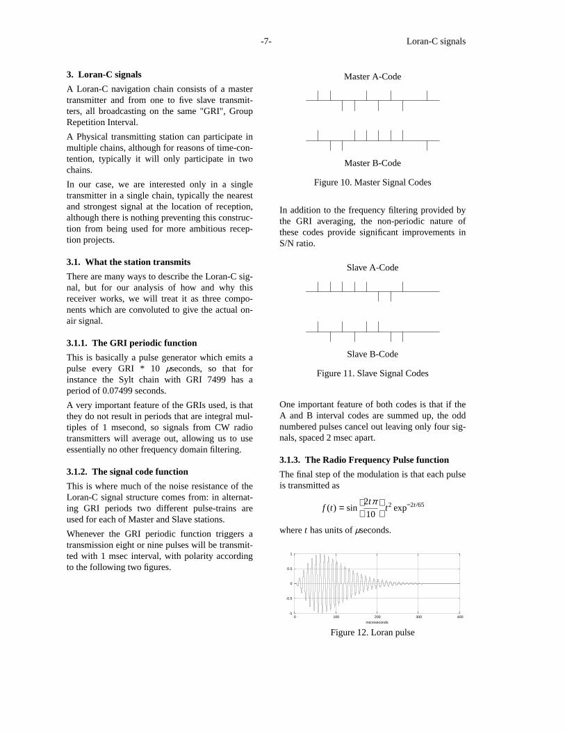
3.1.2. Thesignal code function
This is where much of the noise resistance of theLoran-C signal structure comes from: in alternat-ing GRI periods two different pulse-trains areused for each of Master and Slave stations.
Whenever the GRI periodic function triggers atransmission eight or nine pulses will be transmit-ted with 1 msec interval, with polarity accordingto the following two figures.
Master A-Code
Master B-Code
Figure 10. Master Signal Codes
In addition to the frequency filtering provided bythe GRI averaging, the non-periodic nature ofthese codes provide significant improvements inS/N ratio.
Slave A-Code
Slave B-Code
Figure 11. Slave Signal Codes
One important feature of both codes is that if theA and B interval codes are summed up, the oddnumbered pulses cancel out leaving only four sig-nals, spaced 2 msec apart.
3.1.3. TheRadio Frequency Pulse function
The final step of the modulation is that each pulseis transmitted as
f (t) = sin2tπ10
t2 exp−2t/65
wheret has units ofµseconds.
-1
-0.5
0
0.5
1
0 100 200 300 400
microseconds
Figure 12. Loran pulse

-8- Loran-Csignals
In reality it is only the first part of the pulse-shapewhich is controlled, and in particular, the refer-ence point is the 3rd positive zero-crossing of thesignal
-1
-0.5
0
0.5
1
0 5 10 15 20 25 30 35 40 45 50 55 60 65
microseconds
3rd (positive) zero crossing
Figure 13. Loran pulse front
When we combine all these components, theresult is something like this:
-1
-0.5
0
0.5
1
0 0.2 0.4 0.6 0.8 1
Figure 14. 6731 Lessay chain
All four stations in the Lessay chain are visible inthis plot, first the master in Lessay, notice the"extra" 9th pulse 2 msec after the 8th, the followsthe Xray slave in Soustons, the Yankee slave inRugby and finally the Zulu slave on the island ofSylt.
Knowing the exact geographical locations ofthese four transmitters, and the time interval fromthe master transmission until the slaves transmittheir pulses, we could calculate our geographicposition from the measured time-intervalsbetween these signals.

-9- Reception
4. Reception
So, how do we find and lock onto the Loran-Csignal with only 8 kilobytes of RAM ?
The brute-force method would be to simply aver-age all samples over the FRI interval, that wouldallow us to identify all signals in the chain, tell Aand B codes apart, locate the 3rd zero-crossingand track each signal.
Unfortunately, this would require up to2 ⋅ 9999⋅ 10 = 199980 averaging buckets.
Even if only one bit is used per bucket, thisamounts to 24.5 kilobytes, more than three timesthe amount of RAM we have available.
We can get rid of the factor two by averaging onlyover the GRI interval, and provided we rotateev ery other GRI period one millisecond, we canstill tell the four signal codes apart, at the expenseof recognizing two energy levels in the pulse pat-terns.
+
=
Figure 15. delayed master code average pattern
Unfortunately, that still requires more than 12kilobytes of RAM.
It is possible to implement both of these versionsof the algorithm by looking only at a small win-dow of the GRI or FRI period at a time.
Since we realistically need 16, or preferably 32bits, per bucket, and at best can use around 6 ofthe 8 kilobytes, this would result in at least 33windows, in practice more because of necessaryoverlapping, each of which must be integrated forsome time, before a signal may be appearant.
Instead we this narrow scan, single phaseapproach, we opt for a widescan, multi phaseapproach.
-10- Phasezero
5. PhaseZero - Locating the strongest signal
Our first phase must locate the strongest signal inthe chain, typically the transmitter closest to thereceiving antenna.
When averaged over the GRI period, both themaster and slave codes become four pulses sepa-rated by 2ms and our goal is simply to find thestrongest one of these.
We do not care at this point, if it is a master orslave signal or where the A or B codes are intime, the next phase will figure that out.
Assuming we have 1000 buckets of 32 bits avail-able, we can sample the GRI interval every100µs, and in doing so, we would likely missev en very strong signals: We need a sampling fre-quency which is not a divisor in the 100 kHz car-rier frequency.
Since our goal is to just find the rough location ofthe strongest signal in the GRI, we are not evenconstrained to sample at rates that divide into the1ms pulse spacing, and in fact get better results bynot doing so.
Experiments and simulations has shown that if weav erage every 114µs, every 114th sample, overthe GRI period, we can expect to catch at least30% of the peak amplitude of the strongest signal,and need only 99990µs/114 = 887 buckets.
5.1. Tek4014 view of phase zero
GRI = 7499 "Sylt"state = 0 avg = 8 avg_cur = 7 used = 83
PeakA:1085
Figure 16. Tek4014 view of phase 0
This is how the tek4014 window looks in phasezero, we see the averaging buckets plotted, andthe peak signal is marked.
In the lower left corner of the box is the amplitudeof the signal in ADC units.
Notice that we do in fact quite clearly see all fourpeaks in the averaged signal, but one of them issignificantly taller than the other three.
5.2. Hardware view of phase zero
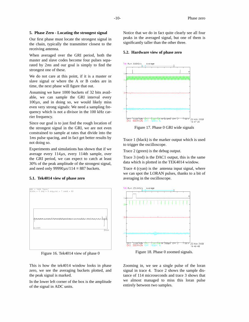
Figure 17. Phase 0 GRI wide signals
Trace 1 (black) is the marker output which is usedto trigger the oscilloscope.
Trace 2 (green) is the debug output.
Trace 3 (red) is the DAC1 output, this is the samedata which is plotted in the TEK4014 window.
Trace 4 (cyan) is theantenna input signal, wherewe can spot the LORAN pulses, thanks to a bit ofav eraging in the oscilloscope.
Figure 18. Phase 0 zoomed signals.
Zooming in, we see a single pulse of the loransignal in trace 4.Trace 2 shows the sample dis-tance of 114 microseconds and trace 3 shows thatwe almost managed to miss this loran pulseentirely between two samples.

-11- Phaseone
6. PhaseOne - Identifying the code
The peak signal from phase 1 must by definitionbe within 57 samples of the true peak value, ofone of the four peaks, 2 msec apart, resultingfrom the GRI summing.
Now we need to find out if this is a master orslave station, and to identify which half of the FRIhas the A and B code.
If we caught the last of the four peaks, the codestarts 6 msec ahead of this point, if we caught thefirst of the four peaks, it spans another 9 msecafter this point, so all in all, there are 16 windowswe need to check for the precense of pulses.
We use a repetition frequency of 2 * GRI, some-times called "FRI" for Frame Repetition Rate, inorder to not add the A and B codes together.
detected peak
search windows
Figure 19. mode1 code windows
Using no more than the 876 integers used inphase zero, each bucket can get 54 integers and ifwe space them 13 samples apart, each bucket willcover 702 µseconds.
Again, 13 is a good number because it will makethe sample points "wander" over the 100 kHzperiod of the pulses.
GRI = 7499 "Sylt"state = 1 avg = 8 avg_cur = 8 used = 205
Master−A 39725179 @ 4:27Master−B 13669117 @ 5:27
Slave−A 25598820 @ 1:27Slave−B 20225303 @ 0:27
Best code: Master−A
90 107 116 97 931
Master−A
1000 823 899 873 861 827 866 180 937 149 148
Figure 20. Tek4014 view of phase 1
The tek4014 view shows the 16 windows andshows the starting point of the strongest code inthem.
Above each window is the energy content of thatwindow, in thousands of the maximum found inany window. Due to timing effects, it is quitelikely that one or two windows show numbersslightly above 1000. Presently, the energylevels isnot used for code identification.
Below the windows are statistics for each of thebest match for each of the four possible codes.
Figure 21. Phase 1 FRI wide signals
This is the hardware view, showing a full FRIinterval.
Notice in trace 4, that we only sample every otherpulse group.
Figure 22. Phase 1 pulse group
Zooming in on the pulse group, we can see intrace 2 how each bucket is sampled and in trace 3the resulting wav eform.
Notice that the pulse shape is not fully recoveredat this point, we only sample every 13

-12- Phaseone
microseconds, but that is plenty to identify thecode.
Figure 23. Phase 1 single pulse
Here we are zoomed into just two pulse windows.

-13- Phasetwo
7. PhaseTw o - Locking on to the signal
Now we hav eall the timing informaton we needto start integrating the signal for good: we knowwhere the maximum is of the first pulse in thecode, and we know which code it is.
In this phase we integrate every ADC conversionin a 750 (XXX: check code) sample windowaround all the 16 or 18 pulses in the signal, intothe same single bucket, taking care to invert thepulses per the code.
GRI = 7499 "Sylt"state = 2 avg = 10 avg_cur = 10 used = 607
PeakA:1314
PeakM x i30 r12 delta r23 delta peak delta err− −−− −−−− −−−− −−−−− −−−− −−−−− −−−− −−−−− −−−−−A 338 864 3498 580 1702 49 1217 − 30 629 0
A
B 343 1045 1997 − 921 1481 − 172 1415 168 1093 2
B
Figure 24. Tek4014 view of phase 2
The tek4014 view shows two views of our inte-gration buffer, with the bottom one zoomed in onthe peak value.
The various candidates for 3rd zero crossings aremarked and their statistics given in numeric formbelow.
Figure 25. Phase 2 FRI view
The MARK pulses are spaced 2 * GRI apart now,and we can see how the signal is sampled twice inthat period.
Figure 26. Phase 2 group view
Zooming in on the group, we can see th ninepulses of the master code being sampled.
Notice in trace 2, that there is a short burst ofsamples in the space between the 8th and 9thpulse, and after the 9th pulse.These samples arenot technically necessary, but are planned forAGC use.
Figure 27. Phase 2 pulse view
Finally zooming in on a single pulse, we can seethe full wav e-shape of the Loran-C pulse, includ-ing the sky-wav eecho.
The small "pre-echo" is currently unexplained.
7.1.

-14- Phasetwo
Figure 28. Finding 3rd zero

-15- Phasethree
8. PhaseThr ee - Tracking the 3rd zero-cross-ing.
In state 3 we have chosen the zero-crossing wewant to track, and hold on to it to the best of ourability.
In practice we cannot simply nail a particularsample in the GRI window and track that, as thesignal and the timebase may wander relative toeach other.
We always use as tracking sample, the sample thatis closest to the 3rd zero crossing.
Nominally the tracking point is sample 75 in thewindow, but we allow it to wander up to 10 sam-ples in either direction, before we realign the sam-pling window to put it back at sample 75.
We interpolate the true zero crossing between thetracking sample and the two samples that sur-round it.
This is the Tek4014 display in phase three:
GRI = 7499 "Sylt"state = 3 avg = 10 avg_cur = 10 used = 2385
TrackA:1331
Track
Track 75 x0 17598379 x1 4823560 x2 −12793746
Phase 0 frac −189 off −189
Figure 29. Tek4014 view of state 3
The top plot shows the entire sampling windowand a marker for the tracking sample.
The bottom plot zooms in and marks both thetracking sample and the two neighboring samples.
Below the plots are the pertinent statistics, includ-ing calculated timing of the 3rd zero crossing.
The three samples which contribute to the inter-polation of the zero crossing, are each filteredwith a FIR bandpass filter:
Figure 30. The FIR filter kernel
-140
-120
-100
-80
-60
-40
-20
0
0 0.05 0.1 0.15 0.2 0.25 0.3 0.35 0.4 0.45 0.5
dB
MHz
Figure 31. The FIR filter frequency response
The exact choice of filter has proven to beremarkably unimportant, but it does in fact reducethe noise in the three sample points considerably.
8.1. Interpolating the zero crossing
Since we want better resolution than the wholemicroseconds the sample rate provides, we needto interpolate the true zerocrossing from the sam-ple values around it:
Yb
Yn
Ya
Tsamp Tsamp
Tx
Figure 32. Interpolating the zero crossing
If we define Yn as the sample that has the lowestabsolute value, closest to the 3rd zero-crossing,we can determine the range ofTx by solving:
Loran(x) = −Loran(x + 1µs) x ∈ [29µs . . .30µs]
Doing so, we findx ≈ 29. 664µs.
It follows that theYn sample must be locatedbetween [29.664µs . . .30. 664µs] and conse-quently thatTx ∈[−337ns . . .664ns].
-16- Phasethree
The analytical solution for findingTx given Yb,Yn andYa is neither practically realizable with thelimited amount of CPU and memory we haveavailable, nor necessary.
Instead we calculate the FIR filtered signal at thesample nearest the zero-crossing (Fn), and the twosamples right before (Fb) and right after (Fa) andfind the ratio:
Fn
Fa − Fb∈ [−0. 2871. . .0. 2679]
Which we map to the corresponding:
Tx → [−337ns . . .664ns]
Using a lookup table containing the precomputedconversion function:
-20
-15
-10
-5
0
5
10
-0.3 -0.2 -0.1 0 0.1 0.2 0.3-400
-200
0
200
400
600
800
ns fr
om li
near
ns a
bsol
ute
ratio
Figure 33. Interpolation non-linearity
The lookup table is built by the scriptpulse_param.tcl and lives in the source filepulse_param.c .
The script automatically reads in the FIR filtercoefficients from thefir.c source file and deter-mines how many entries the lookup table needs tohave, to provide the specified resolution.
The table is extended 5% further than necessaryin both end, to cater for edge effects and noisecomponents.
For a resolution of nanoseconds, the table has1111 entries.
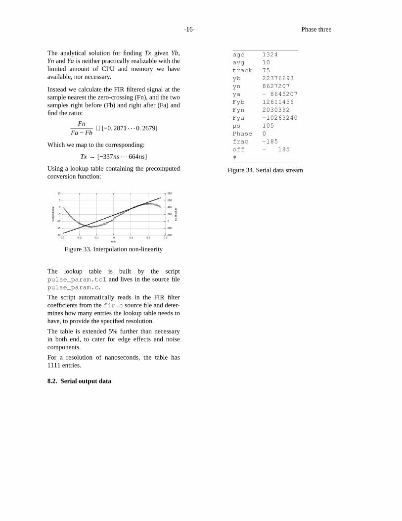
8.2. Serialoutput data
agc 1324avg 10track 75yb 22376693yn 8627207ya - 8645207Fyb 12611456Fyn 2030392Fya -10263240µs 105Phase 0frac -185off - 185#
Figure 34. Serial data stream

-17- Performance
9. Performance
These are some of the first performance data col-lected, and they should therefore be taken with allsensible precaution.
The signal is 7499M, 205 km away.
The exponential averaging factor is 1/1024.
The timebase is a free-runing FRS10 Rb, the sam-ples have been compensated for the randomlychosen, but deliberate 7.225e-10 frequency offset.
A phase measurement is recorded once per sec-ond using Timer2, from approx 2008-11-30 11:00to 2008-12-01 11:00 UTC.
-8e-08
-6e-08
-4e-08
-2e-08
0
2e-08
4e-08
6e-08
8e-08
0 10000 20000 30000 40000 50000 60000 70000 80000 90000
seco
nds
seconds
Figure 35. Raw offset samples
The standardeviation of the raw samples is 22.6nanoseconds.
A histogram of the samples show a gaussian dis-tribution, which seems well suited to more aggre-sive averaging.
-80 -60 -40 -20 0 20 40 60 80
Figure 36. Offset value interval histogram
The modified allan variance is plotted below:
1e-13
1e-12
1e-11
1e-10
1e-09
1e-08
1 10 100 1000 10000 100000
Mod
ified
Alla
nV
aria
nce
τ
Figure 37. Modified allan Variance

-18- Software
10. Software
The software that goes with this article is writte asproof of concept, but is written such that experi-mentation and further development is possible.
10.1. Thetrick y assembler bits
The tricky bit of the software is the assemblercoded fast interrupt routine in the filecrt0.S.
I hav ewritten this code so that it does not encodeany of the high-level logic, but instead mechani-cally walks a chain of structures that tell it what tomeasure and when.
For instance, when we scan the 6731 GRI inphase zero, the specification looks like this:
{mark = 1;ptr = ss->ptr;polarity = "+";avg = 6;cnt = 1;timer_repeat = 114;repeat = 590;timer_after = 50;next = this;
}Figure 38. Phase zero specification
This specification tells the assembler code topulse the MARK pin high when starting this spec-ification, then 590 times take one ADC measure-ment 114 microseconds apart, then skip 50microseconds and start over.
Since 590* 114+ 50 = 67310 this will repeatedlyscan the 6731 GRI signals.
Thepolarity member specifies that the samples allhave positive phase, theavg specifies he exponen-tial average time constant and thenext membertells it what to do next (the same thing).
With none of few modifications, this schemeshould also support reception of multiple stationsin the same chain or even sev eral stations fromdifferent chains.
10.2. Thehigh level logic
The highlevel logic, such as it is, is written in Ccode in theloran0.c file.
Right now the code is semi-manual, controlled bysingle characters received on the serial/USB port,running at 115200 bps.
The following commands are recognized:
c This will present a menu with Loran-C chainsfrom which you can choose one by enteringthe character in the [...].----------------------------------[@] 5543 Calcutta[A] 5930 Canadian East Coast[B] 5980 Russian-American[C] 5990 Canadian West Coast[D] 6042 Bombay[E] 6731 Lessay[F] 6780 China South Sea[G] 7001 Bø[H] 7030 Saudi Arabia South[I] 7270 Newfoundland East Coast[J] 7430 China North Sea[K] 7499 Sylt[L] 7950 Eastern Russia Chayka[M] 7960 Gulf of Alaska[N] 7980 Southeast U.S.[O] 7990 Mediterranean Sea[P] 8000 Western Russia[Q] 8290 North Central U.S.[R] 8390 China East Sea[S] 8830 Saudi Arabia North[T] 8930 North West Pacific[U] 8970 Great Lakes[V] 9007 Eiði[W] 9610 South Central U.S.[X] 9930 East Asia[Y] 9940 U.S. West Coast[Z] 9960 Northeast US[[] 9990 North Pacific----------------------------------Please select chain:
Figure 39. Chain selection menu
t Make TEK4014 plot via serial/USB port
u Zoom in on curves in TEK4014 plots
d Zoom out on curves in TEK4014 plots
a Double the exponential average time constant.
b Half the exponential average time constant.
1 Skip to mode 1
2 Skip to mode 2
10.3. TEK4014plotting
Before windows and mice, Tektronix produced aseries of high quality graphical terminals, basedon the storage-CRT principle.
These plotting instructions to these terminalsbecame the de-facto format for plotting files andas a result, the original X11 "xterm" programoffered, and still does, TEK4014 emulation.
If you connect to the serial/USB port using theX.org xterm program and press ’t’, then you willbe rewarded with a nice plot as seen earlier in thispaper.
If you use another terminal program which doesnot support TEK4014 plotting commands, youwill get a blast of random ASCII characters.
10.4. Utility functions etc.
The other three C language files contains the codeto configure the hardware, code to use theserial/USB port and a function which calculates

-19- Software
basic statistics for an array of integers.
The files divdi3.c, qdivrem.c and divsi3.S, areruntime support files for the GCC compiler.
10.5. Downloading firmware to the ADuC7026
You can either use a JTAG gadget or downloadthe firmware via the serial/USB port.
Included in the source-code package is an "aduc"program I have written for that purpose.
10.6. Compilingthe firmware
Cross-compiling is notoriously tricky, but theFreeBSD build enviroment makes it quite easy.
To build a arm cross-compiler + toolchain, simplydo the following:
cd /usr/srcmake toolchain \
TARGET=arm TARGET_ARCH=arm
Figure 40. Building an ARM toolchain on FreeBSD
The Makefile knows how to find these tools underthe /usr/obj.

-20- Timer1 unexplained
Figure 41. Protocol analyser trace
11. Timer1 unexplained
This is a confession: I have no idea exactly howTimer1 is supposed to work in the ADuC7026chip, and the way I have observed it work bafflesme, but the software manages to work around it.
The PWM section provides us with a 1MHz fre-quency which, through an external pin, becomesTimer1’s clock signal.
In Fig XXX above this external signal is namedPWM, which for this experiment, was give a veryshort "on" time.
The signal named "MARK" is from PLA[5],which is configured so the flip-flop is latched byTimer1’s count-complete signal.
The signal named "ADCBUS" is the ADCbusysignal, which indicates that the ADC has startedperforming a conversion, and the ADC is alsotriggered by Timer1’s count-complete signal.
So far, so good, it looks like Timer1 expiresaround the middle of the figure.
But now look at the "DEBUG" signal, which isprogramatically lowered as the first thing in the
fast interrupt handler, then pulsed high afterTimer1 has been reloaded.
The fast interrupt isalso triggered by Timer1’scount-complete signal, but this happens wellbefore PLA[5] and the ADC receive the signal.
From the FIQ request is raised until the firstinstruction of the handler is executed takes at leastfive clock cycles, but it can take as much as 13(XXX ?) cycles, depending which instruction theCPU was executing.
This is why the "DEBUG" trace shows multipletransititions: it is not deterministic in time.
But he mystery gets deeper here, because the pre-vious PWM signal, presumably the one thatcounds down to one, is a fair bit further ahead ofthe DEBUG signal than 5-13 (XXX) clock cycles.
But it gets more mysterious still: The fast inter-rupt handler loads a value into the T1LD registerright before the high pulse on the DEBUG signal(right of the dotted line).
If the leftmost PWM signal is the 1 count, thenthe central one is the 0 count, it would be reason-able to expect that loading N or N-1 into theT1LD register at this point, would cause the nextTimer1 count complete event to happen N cycles

-21- Timer1 unexplained
of the PWM signal later, starting with the one inthe right hand side of the trace.
Experiementally I have found that I have to loadN-3 to make that happen.
For this to make sense, the PWM edge that trig-gered the count down to zero must be just outsidethe papers left edge so that the central PWM pulseis number 3 in the new counting cycle.
If that is the case, then the chip applies approxi-mately 3µs worth of metastability latching onTimer1s count-complete output, before it reachesthe ARM7TDMI core and the ADC unit.
At the 42MHz clock, 3µ correspond pretty pre-cisely to 128 clock cycles.
If that is the depth of the latch-line that resolvesmetastability, then I would pressume to think thatit is sufficient deep.
Enquiring minds wants to know...