A 64Gb/s PAM-4 Transmitter with 4-Tap FFE and 2.26pJ/b Energy Efficiency in 28nm CMOS FDSOI
28
6.4: A 64Gb/s PAM-4 Transmitter with 4-Tap FFE and 2.26pJ/b Energy Efficiency in 28nm CMOS FDSOI © 2017 IEEE International Solid-State Circuits Conference 1 of 31 A 64Gb/s PAM-4 Transmitter with 4-Tap FFE and 2.26pJ/b Energy Efficiency in 28nm CMOS FDSOI G. Steffan 1 , E. Depaoli 1 , E. Monaco 1 , N. Sabatino 1 , W. Audoglio 1 , A. A. Rossi 1 , S. Erba 1 , M. Bassi 2 , A. Mazzanti 2 1 STMicroelectronics, Pavia, Italy 2 Università degli Studi di Pavia, Pavia, Italy
-
Upload
aiclab -
Category
Engineering
-
view
62 -
download
6
Transcript of A 64Gb/s PAM-4 Transmitter with 4-Tap FFE and 2.26pJ/b Energy Efficiency in 28nm CMOS FDSOI

6.4: A 64Gb/s PAM-4 Transmitter with 4-Tap FFE and 2.26pJ/b Energy Efficiency in 28nm CMOS FDSOI© 2017 IEEE International Solid-State Circuits Conference 1 of 31
A 64Gb/s PAM-4 Transmitter with 4-Tap FFE and 2.26pJ/b Energy Efficiency in
28nm CMOS FDSOI
G. Steffan1, E. Depaoli1, E. Monaco1, N. Sabatino1, W. Audoglio1, A. A. Rossi1,
S. Erba1, M. Bassi2, A. Mazzanti21 STMicroelectronics, Pavia, Italy
2 Università degli Studi di Pavia, Pavia, Italy

6.4: A 64Gb/s PAM-4 Transmitter with 4-Tap FFE and 2.26pJ/b Energy Efficiency in 28nm CMOS FDSOI© 2017 IEEE International Solid-State Circuits Conference 2 of 31
Outline
• Motivation
• Proposed TX Architecture
• Reconfigurable FFE
• Output Driver
• High-Speed Serializer
• Clock Generation
• Measurement Results
• Conclusions

6.4: A 64Gb/s PAM-4 Transmitter with 4-Tap FFE and 2.26pJ/b Energy Efficiency in 28nm CMOS FDSOI© 2017 IEEE International Solid-State Circuits Conference 3 of 31
Network Traffic: Growth and Challenges
72,5
88,7
108,
5
132,
1
160,
6
194,
40
50
100
150
200
2015 2016 2017 2018 2019 2020
Exab
ytes
per M
onth
Challenges• Gate count increases faster than I/O speed• Power dissipation, rather than technology and routing, mostly limits max I/O density• Increasing data rate at > 25Gb/s increases link losses and power consumption
PAM-4 Modulation • Helps maintain loss budget by decreasing Nyquist frequency• SNR degradation can be recovered by using FEC
3x
[Cisco, The Zettabyte Era: Trends and Analysis] [OIF-FD-Client-400G/1T-01.0 White Paper]

6.4: A 64Gb/s PAM-4 Transmitter with 4-Tap FFE and 2.26pJ/b Energy Efficiency in 28nm CMOS FDSOI© 2017 IEEE International Solid-State Circuits Conference 4 of 31
High-Speed PAM-4/NRZ TX Design
High output amplitude and linearity – to
preserve SNR and H/V opening
Very high bandwidth –to speed-up non-
adjacent level transitions
Reconfigurable FFE –to be compliant with several standards
PAM-4/NRZ high/low speed modes – for
auto-negotiation and substitution of legacy
components
Precise and reliable serialization with low
power
Challenges
PAM-4 PAM-4
PAM-4/NRZ
PAM-4/NRZ PAM-4/NRZ

6.4: A 64Gb/s PAM-4 Transmitter with 4-Tap FFE and 2.26pJ/b Energy Efficiency in 28nm CMOS FDSOI© 2017 IEEE International Solid-State Circuits Conference 5 of 31
8:48:48:48:4
8:4
8:4
8:48:4
C-2 C-1 C0
C-2 C-1 C0
C0 C1 C2
C0 C1 C2
LSB
MSB
40b
FFELVdd,CMOS
MM
ML FFEM
4:14:14:14:1
4:14:14:14:1
4x8b 4x4bC-2 C-1 C0
C-2 C-1 C0
C0 C1 C2
C0 C1 C2
8b
C-2 C-1
C0
C1
C2
40:8
C-2 C-1
C0
C1
C2
40:8
5x8b
40b
4x8b 4x4b
8b
5x8b
TX Block Diagram
• Shift-registers delay 8bit bundles and generate five C[-2:2] FFE data-streams• MUXs MM and ML enable C[-2:2] selection• In PAM-4 mode, up to 4 FFE taps • In NRZ mode, 40b LSB/MSB data is merged, but MM and ML can still be operated
independently to provide up to 5 FFE taps

6.4: A 64Gb/s PAM-4 Transmitter with 4-Tap FFE and 2.26pJ/b Energy Efficiency in 28nm CMOS FDSOI© 2017 IEEE International Solid-State Circuits Conference 6 of 31
TX Block Diagram
612246
36123
Out
put N
etw
ork
Vdd,DR
24
48
8:48:48:48:4
8:4
8:4
8:48:4
C-2 C-1 C0
C-2 C-1 C0
C0 C1 C2
C0 C1 C2
LSB
MSB
40b
FFELVdd,CMOS
MM
ML FFEM
4:14:14:14:1
4:14:14:14:1
4x8b 4x4bC-2 C-1 C0
C-2 C-1 C0
C0 C1 C2
C0 C1 C2
8b
C-2 C-1
C0
C1
C2
40:8
C-2 C-1
C0
C1
C2
40:8
5x8b
40b
4x8b 4x4b
8b
5x8b
• Output driver is composed of 72 elements• 24 driver elements are driven by LSB data, 48 by MSB data• Dedicated voltage supply Vdd,DR=1.2V

6.4: A 64Gb/s PAM-4 Transmitter with 4-Tap FFE and 2.26pJ/b Energy Efficiency in 28nm CMOS FDSOI© 2017 IEEE International Solid-State Circuits Conference 7 of 31
TX Block Diagram
612246
36123
Out
put N
etw
ork
Vdd,DR
24
48
8:48:48:48:4
8:4
8:4
8:48:4
C-2 C-1 C0
C-2 C-1 C0
C0 C1 C2
C0 C1 C2
LSB
MSB
40b
FFELVdd,CMOS
MM
ML FFEM
4:14:14:14:1
4:14:14:14:1
4x8b 4x4bC-2 C-1 C0
C-2 C-1 C0
C0 C1 C2
C0 C1 C2
8b
C-2 C-1
C0
C1
C2
40:8
C-2 C-1
C0
C1
C2
40:8
5x8b
40b
4x8b 4x4b
8b
5x8b
REF CK
÷2÷4/5
I/QGeneration
CK4-I
CK4-QPLL 2-8GHz
• PLL generates 2-8GHz clock signal• High precision I/Q signals generator feeds the 40:1 serializer

6.4: A 64Gb/s PAM-4 Transmitter with 4-Tap FFE and 2.26pJ/b Energy Efficiency in 28nm CMOS FDSOI© 2017 IEEE International Solid-State Circuits Conference 8 of 31
Reconfigurable TX FFE
• At Full-Speed, it provides up to 4 FFE tap in PAM-4 mode and 5 tap in NRZ mode, meeting OIF CEI 56Gb/s MR and 28Gb/s KP4 standards
• At Half-Speed, data is oversampled and [C-2 ,C2] are mapped as 1-Pre/Post cursor, respectively, meeting 10Gb/s KR10 and 8.5Gb/s PCI Exp-3
• At Quarter-Speed, C2 is mapped as 1-Postcursor while C-2:1 are all set to the Main cursor. This configurations is compliant with 2.5Gb/s PCI-Exp1
FFEL
3
6
12
3C-1
C-2
C0
C-1
C-2
C0
C1
C0
C2
C1
C0
C2
C2 C1
C0
C-1
C-2 C-2
C-1
C0
C1
C2
6
12
24
6C-1
C-2
C0
C-1
C-2
C0
C1
C0
C2
C1
C0
C2
C2 C1
C0
C-1
C-2 C-2
C-1
C0
C1
C2
FFEM
Out
put N
etw
ork
LSB
MSB
-21/72-3/24
-21/72-21/72
12/2436/7236/72
-9/24-36/72-36/72
-9/24-36/72
2-PRE 1-PRE MAIN 1-POST 2-POST
45/72 -27/72
PAM-4 FSNRZ FSNRZ HSNRZ QS
Coefficients Minimum Normalized Amplitude

6.4: A 64Gb/s PAM-4 Transmitter with 4-Tap FFE and 2.26pJ/b Energy Efficiency in 28nm CMOS FDSOI© 2017 IEEE International Solid-State Circuits Conference 9 of 31
State-of-the-art PAM-4 Output Drivers
• Hybrid voltage/current driver• Very good linearity and high output
amplitude with 1V supply• Bandwidth limited by increased load• Low FFE programmability
• Pure current mode driver• Simple implementation, high
bandwidth• Two supply domain and need of level
shifter operating at output symbol rate• High FFE programmability
[Bassi et al., ISSCC 2016, JSSC 2017] [Nazemi et al., ISSCC 2016]

6.4: A 64Gb/s PAM-4 Transmitter with 4-Tap FFE and 2.26pJ/b Energy Efficiency in 28nm CMOS FDSOI© 2017 IEEE International Solid-State Circuits Conference 10 of 31
Proposed Current Mode Driver
• InN and InP CMOS-level input data streams from serializer• Gate voltages of MC1,2 current sources are constant, set by replica bias based on
desired output swing Vref• When output node is high, MC1,2 source is pulled to Vdd,CMOS, relaxing reliability
constraints and allowing the use of thin oxide devices

6.4: A 64Gb/s PAM-4 Transmitter with 4-Tap FFE and 2.26pJ/b Energy Efficiency in 28nm CMOS FDSOI© 2017 IEEE International Solid-State Circuits Conference 11 of 31
Output Network
• 200V MM / 500V CDM, >>2kV HBM ESDs
• Driver capacitance is comparable with ESD capacitance
• Double T-coil network enhances bandwidth by 1.5 and improves impedance matching at high frequency
Driver
Resistor LoadBankESD
OutPCoil #1
Coil #2
ESD
OutNCoil #1
Coil #2
CBUMPCESDCDRIVERCLOAD
Coil #2Coil #1
-9
-6
-3
0
0 10 20 30
TF [d
B]
Frequency [GHz]
With Coils
Without Coils
-30
-20
-10
0
0 10 20 30
Ret
urn
Loss
[dB]
Frequency [GHz]
With Coils
Without Coils

6.4: A 64Gb/s PAM-4 Transmitter with 4-Tap FFE and 2.26pJ/b Energy Efficiency in 28nm CMOS FDSOI© 2017 IEEE International Solid-State Circuits Conference 12 of 31
High-Speed Serializer Architectures
Half-rate architecture• tBIT > tSetup + tMUX + tDIV – tD• Low CPAR load of half-rate architecture
leads to very fast commutations
Quarter-rate architecture• tBIT > tSetup + tMUX – tPULSE
• Higher CPAR load of quarter-rate architecture leads to increased ISI
Propagating clock forward relaxes serializer timing constraints Low load highly desirable to limit ISI
CK4-I CK4-Q
tMUX
tDIV
CK2
B0
B1
OUT4:2
2:1CPAR
D0
D1
D2
D3
CK4-I
CK4-Q
CK4-I
CK4-Q
FF
FF
FF
FF
tD
/2 CK4-ICK4-Q SEL<3:0>
tPULSE
D0
D1
D2
D3
CK4-I
CK4-Q
SEL<0>
SEL<1>
SEL<2>
SEL<3>CK4-I
CK4-Q
tMUX
FF
FF
FF
FF
2xCPAR
OUT
4:1

6.4: A 64Gb/s PAM-4 Transmitter with 4-Tap FFE and 2.26pJ/b Energy Efficiency in 28nm CMOS FDSOI© 2017 IEEE International Solid-State Circuits Conference 13 of 31

6.4: A 64Gb/s PAM-4 Transmitter with 4-Tap FFE and 2.26pJ/b Energy Efficiency in 28nm CMOS FDSOI© 2017 IEEE International Solid-State Circuits Conference 14 of 31
2
4
6
8
10
12
14
16
18
10 20 30 40 50
Jitte
r Pk-
Pk [p
s]
Symbol Rate[Gsym/s]
Traditional 4:1 Mux
Proposed 4:1 Mux
Proposed MUX Architecture
• MUX 4:2 based on pass-gate to save power and guarantee tMUX > tMULT to respect hold-time constraints
• NAND-based frequency doubler generates half rate clock for the last 2:1 MUX• At 32 Gsym/s the Pk-Pk jitter on output node is reduce by 1.3 compared to a traditional
direct 4:1 MUX
CK4-ICK4-Q X2
tMUX
tMULT
CK2
B0
B1
D0
D2
D1
D3
OUT4:2 2:1
CK4-IP/N
CK4-QP/P
CK4-IN/P
CK4-QN/N
CK2P/N
X2
B0
CK2P
B1
CK2N
OUT
2:1
LAT
D0/D1
D2/D3
CK4-I/CK4-Q
B0/B1
4:2

6.4: A 64Gb/s PAM-4 Transmitter with 4-Tap FFE and 2.26pJ/b Energy Efficiency in 28nm CMOS FDSOI© 2017 IEEE International Solid-State Circuits Conference 15 of 31
Effects of I/Q Mismatches
• I/Q mismatches on quarter-rate clocks creates DCD on half-rate clock• I/Q phase difference must be lower than 1.4°

6.4: A 64Gb/s PAM-4 Transmitter with 4-Tap FFE and 2.26pJ/b Energy Efficiency in 28nm CMOS FDSOI© 2017 IEEE International Solid-State Circuits Conference 16 of 31
Effects of I/Q Duty-Cycle Distortion
• DCD on quarter-rate I/Q clocks translates to DCD on half-rate clocks with period of 4UI

6.4: A 64Gb/s PAM-4 Transmitter with 4-Tap FFE and 2.26pJ/b Energy Efficiency in 28nm CMOS FDSOI© 2017 IEEE International Solid-State Circuits Conference 17 of 31
Clock Generation Tree
• Integer-N type PLL with two VCOs and output divider to generate 2-8GHz master clock
• Injection-Locking Ring Oscillator provides high-accuracy 8 phases against PVTs
• Phase rotators interpolate 8 π/4-spaced phases to improve DNL and INL• Quarter-rate clocks fed to serializer after DCC circuit

6.4: A 64Gb/s PAM-4 Transmitter with 4-Tap FFE and 2.26pJ/b Energy Efficiency in 28nm CMOS FDSOI© 2017 IEEE International Solid-State Circuits Conference 18 of 31
Injection Locked Ring Oscillator
Supply voltage [V]
Temperature [°C]
Qua
drat
ure
phas
e er
ror
[°]
-40 0 40 80 120
8
4
0
-4
-80.8 0.9 1.0 1.1 1.2
a
Qua
drat
ure
phas
e er
ror
[°]
8
4
0
-4
-8
No calibrationAnalog calibration ONAnalog + digital calibration
b
No calibrationAnalog calibration ONAnalog + digital calibration
• A phase detector based on passive mixers measures the quadrature error and continuously tunes the oscillator Vtune for fine phase correction
• Concurrently, a window comparator monitors Vtune and drives digital coarse calibration in background.
• The quadrature phase error is kept lower than 1.5º when supply and temperature variations are between [0.9V, 1.2V] and [-40ºC, 120ºC]
preset
Locking Signal
up
downvTHvTL
clkLF
logiclogicregister
Freq
uenc
y C
ode
Vtune
Buffer
Digital Loop
Analog Loop
fIN=8GHz
[Anzalone et al., ESSCIRC 2016]

6.4: A 64Gb/s PAM-4 Transmitter with 4-Tap FFE and 2.26pJ/b Energy Efficiency in 28nm CMOS FDSOI© 2017 IEEE International Solid-State Circuits Conference 19 of 31
Phase Rotator
• Phase Rotators consists of four slices driven by the ILRO outputs• Each slice consists of 32 differential pair thermometric weighted to reduce switching
glitches and guarantee the monotonicity of the output phase• At 11GHz, the maximum DNL and INL are 0.5 and 1 LSB, respectively
`
ϕ1=135º,ϕ2=180º
`
ϕ1=90º,ϕ2=135º
`
ϕ1=45º,ϕ2=90º
`
ϕ1=0º,ϕ2=45º
<0>
<15>
<0>
<15>
ϕ1P ϕ1N ϕ2P ϕ2N
1
0
-1
DN
L [L
SB]
0
-1
INL
[LSB
]
0.5
-0.5
1
2
-2
-3
-4
Code0 32 64 96 128
= 2GHz with AQC = 11GHz with AQC = 11GHz without AQC
fIN=11GHz from ext

6.4: A 64Gb/s PAM-4 Transmitter with 4-Tap FFE and 2.26pJ/b Energy Efficiency in 28nm CMOS FDSOI© 2017 IEEE International Solid-State Circuits Conference 20 of 31
DCD Correction Circuit
• PMOS and NMOS switches operates independently
• Two 7 bit thermometric code to avoid glitches and guarantee the monotonicity of the correction
• DCD correction circuit capability equal to ±1.5% at 8GHz
INP,N OUTN,P
SELP<6:0>P,N
SELN<6:0>P,N
-2
-1
0
1
2
0 1 2 3 4 5 6 7 8 9 10 11 12 13 14D
CD
@8G
Hz
[%]
CODE

6.4: A 64Gb/s PAM-4 Transmitter with 4-Tap FFE and 2.26pJ/b Energy Efficiency in 28nm CMOS FDSOI© 2017 IEEE International Solid-State Circuits Conference 21 of 31
Chip Photo and Power Break-Down
• 10ML CMOS 28nm FDSOI CMOS from STMicroelectronics• Chips encapsulated in flip-chip BGA packages

6.4: A 64Gb/s PAM-4 Transmitter with 4-Tap FFE and 2.26pJ/b Energy Efficiency in 28nm CMOS FDSOI© 2017 IEEE International Solid-State Circuits Conference 22 of 31

6.4: A 64Gb/s PAM-4 Transmitter with 4-Tap FFE and 2.26pJ/b Energy Efficiency in 28nm CMOS FDSOI© 2017 IEEE International Solid-State Circuits Conference 23 of 31
Output Eyes at 28/56 Gb/s
0.84UI 0.73V0.48UI
0.18V
• FIR setting: [C-1 C0 C1]=[-1/24 18/24 -3/24]
• Vertical opening: 0.18V• Horizontal opening: 0.48UI
• FIR setting: [C-1 C0 C1]=[-1/24 18/24 -3/24]
• Vertical opening: 0.73V• Horizontal opening: 0.84UI
PRBS-9 @ 28Gb/s QPRBS-13 @ 56Gb/s

6.4: A 64Gb/s PAM-4 Transmitter with 4-Tap FFE and 2.26pJ/b Energy Efficiency in 28nm CMOS FDSOI© 2017 IEEE International Solid-State Circuits Conference 24 of 31
Output Eyes at 32/64 Gb/s
0.75UI 0.6V0.36UI
0.14V
PRBS-9 @ 32Gb/s QPRBS-13 @ 64Gb/s
• FIR setting: [C-1 C0 C1]=[-1/24 18/24 -3/24]
• Vertical opening: 0.14V• Horizontal opening: 0.36UI
• FIR setting:[C-1 C0 C1]=[-1/24 18/24 -3/24]
• Vertical opening: 0.6V• Horizontal opening: 0.75UI
6.4: A 64Gb/s PAM-4 Transmitter with 4-Tap FFE and 2.26pJ/b Energy Efficiency in 28nm CMOS FDSOI© 2017 IEEE International Solid-State Circuits Conference 25 of 31
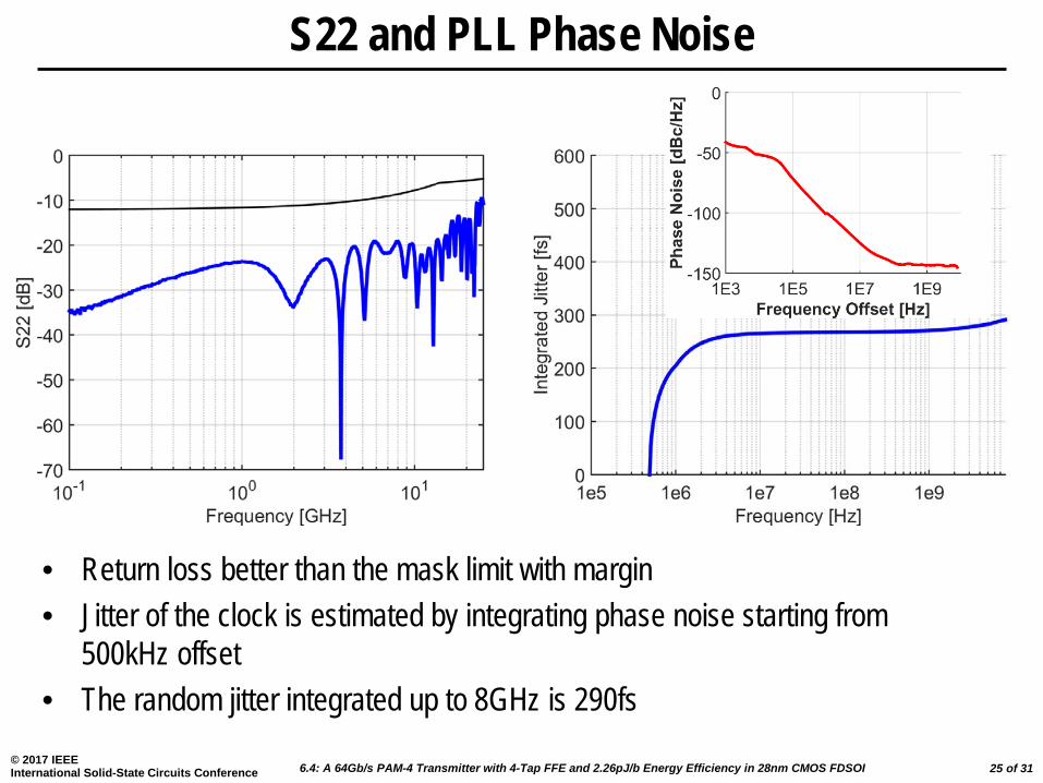
S22 and PLL Phase Noise
• Return loss better than the mask limit with margin• Jitter of the clock is estimated by integrating phase noise starting from
500kHz offset• The random jitter integrated up to 8GHz is 290fs

6.4: A 64Gb/s PAM-4 Transmitter with 4-Tap FFE and 2.26pJ/b Energy Efficiency in 28nm CMOS FDSOI© 2017 IEEE International Solid-State Circuits Conference 26 of 31
Comparison with State of Art

6.4: A 64Gb/s PAM-4 Transmitter with 4-Tap FFE and 2.26pJ/b Energy Efficiency in 28nm CMOS FDSOI© 2017 IEEE International Solid-State Circuits Conference 27 of 31
Conclusions
• Delivering high TX amplitude while preserving linearity and largebandwidth is key for high-speed PAM-4 transmitters
• A new output driver allows high swing and good linearity with increasedsupply while still employing thin-oxide devices operated reliably
• A smart FFE structure is proposed for back-compatibility with legacystandards
• Measurements test chips realized in 28nm CMOS FDSOI technology bySTMicroelectronics prove the effectiveness of the proposed TX

6.4: A 64Gb/s PAM-4 Transmitter with 4-Tap FFE and 2.26pJ/b Energy Efficiency in 28nm CMOS FDSOI© 2017 IEEE International Solid-State Circuits Conference 28 of 31
Acknowledgement
• The authors are thankful to Dr. Guido Albasini, Daniele Baldi and Dr. Davide Sanzogni and the layout team for their contributions