A 200-MHz 64-b dual-issue CMOS microprocessor - Solid ...
13
1555 IEEE JOURNAL OF SOLID-STATE CIRCUITS, VOL. 27, NO. II. NOVEMBER 1992 A 200-MHz 64-b Dual-Issue CMOS Microprocessor Daniel W. Dobberpuhl, Member, IEEE, Richard T. Witek, Randy Allmon, Robert Anglin, David Bertucci, Sharon Britton, Linda Chao, Member, IEEE, Robert A. Conrad, Daniel E. Dever, Bruce Gieseke, Soha M. N. Hassoun, Gregory W. Hoeppner, Member, IEEE, Kathryn Kuchler, Member, IEEE, Maureen Ladd, Member, IEEE, Burton M. Leary, Liam Madden, Edward J. McLellan, Derrick R. Meyer, James Montanaro, Donald A. Priore, Vidya Rajagopalan, Sridhar Samudrala, and Sribalan Santhanam Abstract-A 400-MIPS/200-MFLOPS (peak) custom 64-b VLSI CPU chip is described. The chip is fabricated in a 0.75- pm CMOS technology utilizing three levels of metalization and optimized for 3.3-V operation. The die size is 16.8 mm X 13.9 mm and contains 1.68M transistors. The chip includes separate 8-kilobyte instruction and data caches and a fully pipelined floating-point unit (FPU) that can handle both IEEE and VAX standard floating-point data types. It is designed to execute two instructions per cycle among scoreboarded integer, floating- point, address, and branch execution units. Power dissipation is 30 W at 200-MHz operation. I. INTRODUCTION RISC-style microprocessor has been designed and A tested that operates up to 200 MHz. The chip imple- ments a new 64-b architecture, designed to provide a huge linear address space and to be devoid of bottlenecks that would impede highly concurrent implementations. Fully pipelined and capable of issuing two instructions per clock cycle, this implementation can execute up to 400 million operations per second. The chip includes an 8-kilobyte I-cache, 8-kilobyte D-cache and two associated transla- tion look-aside buffers, a four-entry 32-byte/entry write buffer, a pipelined 64-b integer execution unit with a 32-entry register file, and a pipelined floating-point unit (FPU) with an additional 32 registers. The pin interface includes integral support for an external secondary cache. The package is a 431-pin PGA with 140 pins dedicated to VDD/Vss. The chip is fabricated in 0.75-pm n-well CMOS Manuscript received April 13, 1992; revised June 23, 1992. D. W. Dobberpuhl, R. Allmon, R. Anglin, S. Britton, L. Chao, R. A. Conrad, D. E. Dever, B. Gieseke, K. Kuchler, M. Ladd, B. M. Leary, L. Madden, E. J. McLellan, D. R. Meyer, J. Montanaro, D. A. Priore, V. Rajagopalan, S. Samudrala, and S. Santhanam are with the Semiconductor Engineering Group, Digital Equipment Corporation, Hudson, MA 01749. R. T. Witek was with the Semiconductor Engineering Group, Digital Equipment Corporation, Hudson, MA 01749. He is now with Apple Com- puter, Inc., Austin, TX. D. Bertucci was with the Semiconductor Engineering Group, Digital Equipment Corporation, Hudson, MA 01749. He is now with Sun Micro- systems Inc., Mountain View, CA. S. M. N. Hassoun was with the Semiconductor Engineering Group, Dig- ital Equipment Corporation, Hudson, MA 01749. She is now with the Computer Systems Engineering Department, University of Washington, Seattle, WA 98195. G. W. Hoeppner was with the Semiconductor Engineering Group, Dig- ital Equipment Corporation, Hudson, MA 01749. He is now with the Ad- vanced Workstation Division, IBM Corporation, Austin, TX. IEEE Log Number 9202810. with three layers of metalization. The die measures 16.8 mm x 13.9 mm and contains 1.68 million transistors. Power dissipation is 30 W from a 3.3-V supply at 200 MHz. 11. CMOS PROCESS TECHNOLOGY The chip is fabricated in a 0.75-pm 3.3-V n-well CMOS process optimized for high-performance microprocessor design. Process characteristics are shown in Table I. The thin gate oxide and short transistor lengths result in the fast transistors required to operate at 200 MHz. There are no explicit bipolar devices in the process as the incremen- tal process complexity and cost were deemed too large in comparison to the benefits provided-principally more area-efficient large drivers such as clock and I/O. The metal structure is designed to support the high op- erating frequency of the chip. Metal 3 is very thick and has a relatively large pitch. It is important at these speeds to have a low-resistance metal layer available for power and clock distribution. It is also used for a small set of special signal wires such as the data buses to the pins and the control wires for the two shifters. Metal 1 and metal 2 are maintained at close to their maximum thickness by planarization and by filling metal 1 and metal 2 contacts with tungsten plugs. This removes a potential weak spot in the electromigration characteristics of the process and allows more freedom in the design without compromising reliability. 111. ALPHAARCHITECTURE The computer architecture implemented is a 64-b load/ store RISC architecture with 168 instructions, all 32 b wide [l]. Supported data types include 8-, 16-, 32-, and 64-b integers and 32- and 64-b floats of both DEC and IEEE formats. The two register files, integer and floating point, each contains 32 entries of 64 b with one entry in each being a hardwired zero. The program counter and virtual address are 64 b. Implementations can subset the virtual address size but are required to check the full 64-b address for sign extension. This insures that when later implementations choose to support a larger virtual ad- dress, programs will still run and not find addresses that have dirty bits in the previously “unused” bits. 0018-9200/92$03.00 0 1992 IEEE
Transcript of A 200-MHz 64-b dual-issue CMOS microprocessor - Solid ...
1555 IEEE JOURNAL OF SOLID-STATE CIRCUITS, VOL. 27, NO. I I . NOVEMBER 1992
A 200-MHz 64-b Dual-Issue CMOS Microprocessor Daniel W. Dobberpuhl, Member, IEEE, Richard T. Witek, Randy Allmon, Robert Anglin, David Bertucci,
Sharon Britton, Linda Chao, Member, IEEE, Robert A. Conrad, Daniel E. Dever, Bruce Gieseke, Soha M. N. Hassoun, Gregory W. Hoeppner, Member, IEEE, Kathryn Kuchler, Member, IEEE,
Maureen Ladd, Member, IEEE, Burton M. Leary, Liam Madden, Edward J. McLellan, Derrick R. Meyer, James Montanaro, Donald A. Priore, Vidya Rajagopalan,
Sridhar Samudrala, and Sribalan Santhanam
Abstract-A 400-MIPS/200-MFLOPS (peak) custom 64-b VLSI CPU chip is described. The chip is fabricated in a 0.75- pm CMOS technology utilizing three levels of metalization and optimized for 3.3-V operation. The die size is 16.8 mm X 13.9 mm and contains 1.68M transistors. The chip includes separate 8-kilobyte instruction and data caches and a fully pipelined floating-point unit (FPU) that can handle both IEEE and VAX standard floating-point data types. It is designed to execute two instructions per cycle among scoreboarded integer, floating- point, address, and branch execution units. Power dissipation is 30 W at 200-MHz operation.
I. INTRODUCTION RISC-style microprocessor has been designed and A tested that operates up to 200 MHz. The chip imple-
ments a new 64-b architecture, designed to provide a huge linear address space and to be devoid of bottlenecks that would impede highly concurrent implementations. Fully pipelined and capable of issuing two instructions per clock cycle, this implementation can execute up to 400 million operations per second. The chip includes an 8-kilobyte I-cache, 8-kilobyte D-cache and two associated transla- tion look-aside buffers, a four-entry 32-byte/entry write buffer, a pipelined 64-b integer execution unit with a 32-entry register file, and a pipelined floating-point unit (FPU) with an additional 32 registers. The pin interface includes integral support for an external secondary cache. The package is a 431-pin PGA with 140 pins dedicated to VDD/Vss. The chip is fabricated in 0.75-pm n-well CMOS
Manuscript received April 13, 1992; revised June 23, 1992. D. W. Dobberpuhl, R. Allmon, R. Anglin, S. Britton, L. Chao, R. A.
Conrad, D. E. Dever, B. Gieseke, K. Kuchler, M. Ladd, B. M. Leary, L. Madden, E. J . McLellan, D. R. Meyer, J . Montanaro, D. A. Priore, V. Rajagopalan, S. Samudrala, and S. Santhanam are with the Semiconductor Engineering Group, Digital Equipment Corporation, Hudson, MA 01749.
R. T. Witek was with the Semiconductor Engineering Group, Digital Equipment Corporation, Hudson, MA 01749. He is now with Apple Com- puter, Inc., Austin, TX. D. Bertucci was with the Semiconductor Engineering Group, Digital
Equipment Corporation, Hudson, MA 01749. He is now with Sun Micro- systems Inc., Mountain View, CA.
S. M. N. Hassoun was with the Semiconductor Engineering Group, Dig- ital Equipment Corporation, Hudson, MA 01749. She is now with the Computer Systems Engineering Department, University of Washington, Seattle, WA 98195.
G. W. Hoeppner was with the Semiconductor Engineering Group, Dig- ital Equipment Corporation, Hudson, MA 01749. He is now with the Ad- vanced Workstation Division, IBM Corporation, Austin, TX.
IEEE Log Number 9202810.
with three layers of metalization. The die measures 16.8 mm x 13.9 mm and contains 1.68 million transistors. Power dissipation is 30 W from a 3.3-V supply at 200 MHz.
11. CMOS PROCESS TECHNOLOGY The chip is fabricated in a 0.75-pm 3.3-V n-well CMOS
process optimized for high-performance microprocessor design. Process characteristics are shown in Table I. The thin gate oxide and short transistor lengths result in the fast transistors required to operate at 200 MHz. There are no explicit bipolar devices in the process as the incremen- tal process complexity and cost were deemed too large in comparison to the benefits provided-principally more area-efficient large drivers such as clock and I/O.
The metal structure is designed to support the high op- erating frequency of the chip. Metal 3 is very thick and has a relatively large pitch. It is important at these speeds to have a low-resistance metal layer available for power and clock distribution. It is also used for a small set of special signal wires such as the data buses to the pins and the control wires for the two shifters. Metal 1 and metal 2 are maintained at close to their maximum thickness by planarization and by filling metal 1 and metal 2 contacts with tungsten plugs. This removes a potential weak spot in the electromigration characteristics of the process and allows more freedom in the design without compromising reliability.
111. ALPHA ARCHITECTURE The computer architecture implemented is a 64-b load/
store RISC architecture with 168 instructions, all 32 b wide [l]. Supported data types include 8-, 16-, 32-, and 64-b integers and 32- and 64-b floats of both DEC and IEEE formats. The two register files, integer and floating point, each contains 32 entries of 64 b with one entry in each being a hardwired zero. The program counter and virtual address are 64 b. Implementations can subset the virtual address size but are required to check the full 64-b address for sign extension. This insures that when later implementations choose to support a larger virtual ad- dress, programs will still run and not find addresses that have dirty bits in the previously “unused” bits.
0018-9200/92$03.00 0 1992 IEEE

1556
Feature Size Channel Length Gate Oxide
Power Supply Substrate Salicide Buried Contact Metal 1 Metal 2 Metal 3
VTNI V T P
TABLE I PROCESS DESCRIPTION
0.75 pm 0.5 pm 10.5 nm 0.5 V/-0.5 V 3 . 3 v P-epi with n-well Cobalt disilicide in diffusions and gates Titanium nitride 0.75-m AICu, 2.25-pm pitch (contacted) 0.75-m AlCu, 2.625-pm pitch (contacted) 2.0-m AICu, 7.5-pm pitch (contacted)
IEEE JOURNAL OF SOLID-STATE CIRCUITS, VOL. 21. NO, 1 1 , NOVEMBER 1992
The architecture is designed to support high-speed multi-issue implementations. To this end the architecture does not include condition codes, instructions with fixed source or destination registers, or byte writes of any kind (byte operations are supported by extract and merge in- structions within the CPU itself). Also, there are no first- generation artifacts that are optimized around today's technology, which would represent a long-term liability to the architecture.
IV . CHIP MICROARCHITECTURE The block diagram (Fig. 1) shows the major functional
blocks and their interconnecting buses, most of which are 64 b wide. The chip implements four functional units: the integer unit (IRF + EBOX), the floating-point unit (FRF + FBOX), the load/store unit (ABOX), and the branch unit (distributed). The bus interface unit (BIU), described in the next section, handles all communication between the chip and external components. The microphotograph (Fig. 2) shows the boundaries of the major functional units. The dual-issue rules are a direct consequence of the register-file ports, the functional units, and the I-cache interface. The integer register file (IRF) has two read ports and one write port dedicated to the integer unit, and two read and one write port shared between the branch unit and the load store unit. The floating-point register file (FRF) has two read ports and one write port dedicated to the floating unit, and one read and one write port shared between the branch unit and the load store unit. This leads to dual-issue rules that are quite general:
any load/store in parallel with any operate, an integer op in parallel with a floating op, a floating op and a floating branch, an integer op and an integer branch,
except that integer store and floating operate and floating store and integer operate are disallowed as pairs.
As shown in Fig. 3(a), the integer pipeline is seven stages deep, where each stage is a 5-ns clock cycle. The first four stages are associated with instruction fetching, decoding, and scoreboard checking of operands. Pipeline stages 0 through 3 can be stalled. Beyond 3, however, all pipeline stages advance every cycle. Most ALU opera- tions complete in cycle 4 allowing single-cycle latency, with the shifter being the exception. Primary cache ac-
1 Fig.
1 - 1 A Write BuWer tkzw-l
1. CPU chip block diagram.
Fig. 2 . Chip microphotograph.
ALUI
PC Gel
VA Ge
(a)
Add L I D SHIFT A W R n d FRFWrite
3X Mull Mu12 AddlRnd FRFWrite
(b)
Fig. 3 . (a) Integer unit pipeline timing. (b) Floating-point unit pipeline timing.
cesses complete in cycle 6, so cache latency is three cycles. The chip will do hits under misses to the primary DCACHE.

I I
DOBBERPUHL et al . : 200-MHz 64-b DUAL-ISSUE CMOS MICROPROCESSOR 1557
The ISTREAM is based on autonomous prefetching in cycles 0 and 1 with the final resolution of ICACHE hit not occurring until cycle 5. The prefetcher includes a branch history table and a subroutine return stack. The architecture provides a convention for compilers to pre- dict branch decisions and destination addresses including those for register indirect jumps. The penalty for branch mispredict is four cycles.
The floating-point unit is a fully pipelined 64-b float- ing-point processor that supports both VAX standard and IEEE standard data types and rounding modes. It can gen- erate a 64-b result every cycle for all operations except division. As shown in Fig. 3(b), the floating-point pipe- line is identical and mostly shared with the integer pipe- line in stages 0 through 3, however, the execution phase is three cycles longer. All operations, 32 and 64 b, (ex- cept division) have the same timing. Division is handled by a nonpipelined, single bit per cycle, dedicated division unit.
In cycle 4, the register file data are formatted to frac- tion, exponent, and sign. In the first-stage adder, expo- nent difference is calculated and a 3 x multiplicand is gen- erated for multiplies. In addition, a predictive leading 1 or 0 detector using the input operands is initiated for use in result normalization. In cycles 5 and 6, for addlsub- tract, alignment or normalization shift and sticky-bit cal- culation are performed. For both single- and double-pre- cision multiplication, the multiply is done in a radix-8 pipelined array multiplier. In cycles 7 and 8 , the final ad- dition and rounding are performed in parallel and the final result is selected and driven back to the register file in cycle 9. With an allowed bypass of the register write data, floating-point latency is six cycles.
The CPU contains all the hardware necessary to sup- port a demand paged virtual memory system. It includes two translation look-aside buffers to cache virtual to phys- ical address translations. The instruction translation buffer contains 12 entries, eight that map 8-kilobyte pages and four that map 4-megabyte pages. The data translation buffer contains 32 entries that can map 8-kilobyte, 64-kilobyte, 5 12-kilobyte or 4-megabyte pages.
The CPU supports performance measurement with two counters that accumulate system events on the chip such as dual-issue cycles and cache misses or external events through two dedicated pins that are sampled at the se- lected system clock speed.
V. EXTERNAL INTERFACE The external interface (Fig. 4) is designed to directly
support an off-chip backup cache that can range in size from 128 kilobytes to 16 megabytes and can be con- structed from standard SRAM’s. For most operations, the CPU chip accesses the cache directly in a combinatorial loop by presenting an address and waiting N CPU cycles for control, tag, and data to appear, where N is a mode- programmable number between 3 and 16 set at power-up time. For writes, both the total number of cycles and the
adr I c
CPU CHIP
SvsClk i M r hc125, -
Fig. 4. CPU external interface.
-
MEM SYS UF
-
duration and position of the write signal are programma- ble in units of CPU cycles. This allows the system de- signer to select the size and access time of the SRAM’s to match the desired price/performance point.
The interface is designed to allow all cache policy de- cisions to be controlled by logic external to the CPU chip. There are three control bits associated with each back-up cache (BCACHE) line: valid, shared, and dirty. The chip completes a BCACHE read as long as valid is true. A write is processed by the CPU only if valid is true and shared is false. When a write is performed the dirty bit is set to true. In all other cases, the chip defers to an external state machine to complete the transaction. This state ma- chine operates synchronously with the SYS-CLK output of the chip, which is a mode-controlled submultiple of the CPU clock rate ranging from divide by 2 to divide by 8. It is also possible to operate without a back-up cache.
As shown in the diagram, the external cache is con- nected between the CPU chip and the system memory in- terface. The combinatorial cache access begins with the desired address delivered on the a d r h lines and results in ctl, tag, data, and check bits appearing at the chip receiv- ers within the prescribed access time. In 128-b mode, BCACHE accesses require two external data cycles to transfer the 32-byte cache line across the 16-byte pin bus. In 64-b mode, it is four cycles. This yields a maximum backup cache read bandwidth of 1.2 gigabyte/s and a write bandwidth of 71 1 megabyte/s. Internal cache lines can be invalidated at the rate of one line/cycle using the dedicated invalidate address pins, iAdr-h ( 12 : 5).
In the event external intervention is required, a request code is presented by the CPU chip to the external state machine in the time domain of the SYS-CLK as described previously. Fig. 5 shows the read miss timing where each cycle is a SYS-CLK cycle. The external transaction starts with the address, the quadword within block and instruc- tionldata indication supplied on the cWMask-h pins, and READBLOCK function supplied on the cReq-h pins. The external logic returns the first 16 bytes of data on the data-h and ecc or parity on the check-h pins. The CPU latches the data based on receiving acknowledgment on

I
1558
0 ' 1 I 2 I S I 4
eyeCLKOut-h
pdr-h Y Wild x cW&h vau x x
Fig. 5. CPU extemal timing.
rdAck-H. The diagram shows a stall cycle (cycle 4) be- tween the request and the return data; this depends on the external logic and could range from zero to many cycles. The second 16 bytes of data are returned in the same way with rdAck-h signaling the return of the data and cAck-h signaling the completion of the transaction. cReq-h re- turns to idle and a new transaction can start at this time.
The chip implements a novel set of optional features supporting chip and module test. When the chip is reset, the first attempted action is to read from a serial read-only memory (SROM) into the I-cache via a private three-wire port. The CPU is then enabled and the PC is forced to 0. Thus, with only three functional components (CPU chip, SROM, and clock input) a system is able to begin exe- cuting instructions. This initial set of instructions is used to write the bus control registers inside the CPU chip to set the cache timing and to test the chip and module from the CPU out. After the SROM loads the I-cache, the pins used for the SROM interface are enabled as serial-in and out ports. These ports can be used to load more data or to return status of testing and setup.
VI. CIRCUIT IMPLEMENTATION Many novel circuit structures and detailed analysis
techniques were developed to support the clock rate in conjunction with the complexity demanded by the con- currence and wide data paths. The clocking method is sin- gle wire level sensitive. The bus interface unit operates from a buffered version of the main clock. Signals that cross this interface are deskewed to eliminate races. This clocking method eliminates dead time between phases and requires only a single clock signal to be routed throughout the chip.
One difficulty inherent in this clocking method is the substantial load on the clock node, 3.25 nF in our design. This load and the requirement for a fast clock edge led us to take particular care with clock routing and to do exten- sive analysis on the resulting grid. Fig. 6 shows the dis- tribution of clock load among the major functional units. The clock drives into a grid of vertical metal 3 and hori-
F 373pF
IDI iiEE53~i~ Total Clock Load = 3.2nF
Total Bypass Cap = 128nF
I (~otal Effective Switching Cap = 12.5nF)
Fig. 6. Clock load distribution.
zontal metal 2. Most of the loading occurs in the integer and floating-point units that are fed from the most robust metal 3 lines. To ensure the integrity of the clock grid across the chip, the grid was extracted from the layout and the resulting network, which contained 63 000 RC ele- ments, was simulated using a circuit simulation program based on the AWEsim simulator from Carnegie-Mellon University. Fig. 7 shows a three-dimensional represen- tation of the output of this simulation and shows the clock delay from the driver to each of the 63 000 transistor gates connected to the clock grid.
The 200-MHz clock signal is fed to the driver through a binary fanning tree with five levels of buffering. There is a horizontal shorting bar at the input to the clock driver to help smooth out possible asymmetry in the incoming wavefront. The driver itself consists of 145 separate ele- ments each of which contains four levels of prescaling into a final output stage that drives the clock grid.
The clock driver and predriver represent about 40% of the total effective switching capacitance determined by power measurement to be 12.5 nF (worst case including output pins). To manage the problem of d i ld t on the chip power pins, explicit decoupling capacitance is provided on-chip. This consists of thin oxide capacitance that is distributed around the chip, primarily under the data buses. In addition, there are horizontal metal 2 power and clock shorting straps adjacent to the clock generator and the thin oxide decoupling cap under these lines supplies charge to the clock driver. di ld t for the driver alone is about 2 X 10" A/s. The total decoupling capacitance as extracted from the layout measures 128 nF. Thus the ratio of decoupling capacitance to switching cap is about 10 : 1. With this capacitance ratio, the decoupling cap could sup- ply all the charge associated with a complete CPU cycle with only a 10% reduction in the on-chip supply voltage.
A. Latches
As previously described, the chip employs a single- phase approach with nearly all latches in the core of the chip receiving the clock node, CLK, directly. A repre-

I I
DOBBERPUHL et al.: 200-MHz 64-b DUAL-ISSUE CMOS MICROPROCESSOR
< 2.93Et01
5.86Et01
8.79Et01
1.17Et02
& 1.47Et02
Fig. 7 . CPU clock skew.
sentative example is illustrated in Fig. 8. Notice that L1 and L2 are transparent latches separated by random logic and are not simultaneously active: L1 is active when CLK is high and L2 is active when CLK is low. The minimum number of delays between latches is zero and the maxi- mum number of delays is constrained only by the cycle time and the details of any relevant critical paths. The bus interface unit, many data-path structures, and some criti- cal paths deviate from this approach and use buffered ver- sions and/or conditionally buffered versions of CLK. The resulting clock skew is managed or eliminated with spe- cial latch structures.
The latches used in the chip can be classified into two categories: custom and standard. The custom latches were used to meet the unique needs of data-path structures and the special constraints of critical paths. The standard latches were used in the design of noncritical control and in some data-path applications. These latches were de- signed prior to the start of implementation and were in- cluded in the library of usable elements for logic synthe- sis. All synthesized logic used only this set of latches.
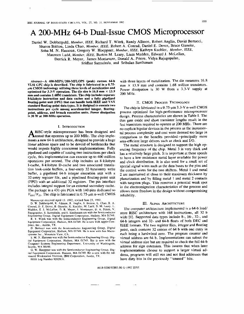
The standard latches are extensions of previously pub- lished work [2] and examples are shown in Figs. 9- 1 1. To understood the operation of these latches refer to Fig. 9(a). When CLK is high, P 1, N1, and N 3 function as an inverter complementing IN1 to produce X. P 2 , N2, and N4 function as a second inverter and complement X to produce OUT. Therefore, the structure passes IN1 to OUT. Then CLK is “low,” N 3 and N 4 are cut off. If IN1, X, and OUT are initially “high,” “low,” and “high,” respectively, a transition of IN 1 FALLING pulls X “high” through P 1 causing P 2 to cut off, which tri- states OUT “high.” If IN1, X, and OUT are initially “low,” “high,” and “low,” respectively, a transition of IN1 RISING causing P 1 to cut off, which tristates X “high” leaving OUT tristated “low.” In both cases, ad- ditional transitions of IN1 leave X tristated or driven “high” with OUT tristated to its initial value. Therefore,
1559
Ll aMm KolMR K1RM(BmReM Ll-
(b)
Fig. 8 . (a) Latching schema. (b) Latch timing.
the structure implements a latch that is transparent when CLK is “high” and opaque when CLK is “low.” Fig. 9(c) shows the dual of the latch just discussed; this struc- ture implements a latch that is transparent when CLK is “low” and opaque when CLK is “high.” Fig. 9(b) and (d) depicts latches with an output buffer used to protect the sometimes dynamic node OUT and to drive large loads.
The design of the standard latches stressed three pri- mary goals: flexibility, immunity to noise, and immunity to race-through. To achieve the desired flexibility, a va- riety of latches like those in Figs. 9-11 in a variety of sizes were characterized for the implementors. Thus, the designer could select a latch with an optional output buffer and an embedded logic function that was sized appropri- ately to drive various loads. Furthermore, it was decided to allow zero delay between latches, completely freeing the designer from race-through considerations when de- signing static logic with these latches.
I560
M
IN! -cp- OUT
Ns N4
M IN! Zm N2
Fig. 9. (a) Noninverting active-high latch. (b) Inverting active-high latch. (c) Noninverting active-low latch. (d) Inverting active-low latch.
IEEE JOURNAL OF SOLID-STATE CIRCUITS, VOL. 21. NO. I I , NOVEMBER 1992
&L ’r-
In the circuit methodology adopted for the implemen- tation, only one node, X(Fig. 9(a)), poses inordinate noise margin risk. As noted above, X may be tristated “high” with OUT tristated “low” when the latch is opaque. This
A
(d)
Fig. 10. (a) Two input AND active-high latch. (b) Two-input NAND active- high latch. (c) Two-input AND active-low latch. (d) Two-input NAND active- low latch.
maps into a dynamic node driving into a dynamic gate that is very sensitive to noise that reduces the voltage on X, causing leakage through P2, thereby destroying OUT.

I I
DOBBERPUHL er al.: 200-MHz 64-b DUAL-ISSUE CMOS MICROPROCESSOR 1561
M
IN1
M
“ I d
lm - I
This problem was addressed by the addition of P5. This weak feedback device is sized to source enough current to counter reasonable noise and hold P2 in cutoff. N5 plays an analogous role in Fig. 9(c).
Race-through was the major functional concern with the latch design. It is aggravated by clock skew, the variety of available latches and the zero delay goal between latches. The clock skew concern was actually the easiest to address. If data propagate in a direction that opposes the propagation of the clock wavefront, clock skew is functionally harmless and tends only to reduce the effec- tive cycle time locally. Minimizing this effect is of con- cern when designing the clock generator. If data propa- gate in a direction similar to the propagation of the clock wavefront, clock skew is a functional concern. This was addressed by radially distributing the clock from the cen- ter of the chip. Since the clock wavefront moves out ra- dially from the clock driver toward the periphery of the die, it is not possible for the data to overtake the clock if the clock network is properly designed.
To verify the remaining race-through concerns, a mix and match approach was taken. All reasonable combina- tions of latches were cascaded together and simulated. The simulations were stressed by eliminating all interconnect and diffusion capacitance and by pushing each device into a comer of the process that emphasized race-through. Then many simulations with varying CLK rise and fall times, temperatures, and power supply voltages were per- formed. The results showed no appreciable evidence of race-through for CLK rise and fall times at or below 0.8 ns. With 1.0-ns rise and fall times, the latches showed signs of failure. To guarantee functionality, CLK was specified and designed to have an edge rate of less than 0.5 ns. This was not a serious constraint since other cir- cuits in the chip required similar edge rates of the clock.
A last design issue worth noting is the feedback de- vices, N5 and P5, in Figs. 1O(c), 10(d), l l (a) , and l l (b) . Notice that these devices have their gates tied to CLK instead of OUT like the other latches. This difference is required to account for an effect not present in the other latches. In these latches a stack of devices is connected to node X without passing through the clocked transistors P3 or N3. Referring to Fig. l l (a ) , assume CLK is “low,” X is “high,” and OUT is “low.” If multiple random transitions are allowed by IN1 with IN2 “high,” then coupling through P 1 can drive X down by more than a threshold even with weak feedback, thereby destroying OUT. To counter this phenomenon, P5 cannot be a weak feedback device and therefore cannot be tied to OUT if the latch is to function properly when CLK is “high.” Note that taller stacks aggravate this problem because the devices become larger and there are more devices to par- ticipate in coupling. For this reason stacks in these latches were limited to three high. Also, note that clocking P5 introduces another race-through path since X will uncon- ditionally go “high” with CLK falling and OUT must be
straint: P5 must be large enough to counter coupling and
Fig. 1 1 . (a) Two-input OR active-high latch. (b) Two-input NOR active- high latch. (c) Two-input OR active-low latch. (d) Two-input NOR active- to retain a stored ONE. there is a two-sided con- low latch.

I
1562 IEEE JOURNAL OF SOLID-STATE CIRCUITS, VOL. 27, NO. I I , NOVEMBER 1992
RESULT RESULT RESULT RESULT RESULT RESULT RESULT RESULT
LATCH
INPUT OPERANDS INPUT OPERANDS INPUT OPERANDS INPUT OPERANDS INPUT OPERANDS INPUT OPERANDS INPUT OPERANDS
BYTE 7 BYTE 6 BYTE 5 BYTE 4 BYTE 3 BYTE 2 BYTE 1
INPUT OPERANDS
BYTE 0
Fig. 12. 64-b adder block diagram
small enough not to cause race-through. These trade-offs were analyzed by simulation in manner similar to the one outlined above.
B. 64-b Adder A difficult circuit problem was the 64-b adder portion
of the integer and floating-point ALU’s. Unlike a pre- vious high-speed design [3], we set a goal to achieve sin- gle-cycle latency in this unit. Fig. 12 has an organiza- tional diagram of its structure. Every path through the adder includes two latches, allowing fully pipelined op- eration. The result latches are shown explicitly in the dia- gram, however, the input latches are somewhat implicit, taking advantage of the predischarge characteristics of the carry chains. The complete adder is a combination of three methods for producing a binary add: a byte-long carry chain, a long-word (32 b) carry select, and local logarith- mic carry select [4]. The carry select is built as a set of nMOS switches that direct the data from byte carry chains. The 32-b long-word lookahead is implemented as a dis- tributed differential circuit controlling the final stage of the upper longword switches. The carry chains are orga- nized in groups of 8 b.
Carry chain width was chosen to implement a byte compare function specified by the architecture. The carry chain implemented with nMOS transistors is shown in Fig. 13(a). Operation begins with the chain predischarged to Vss, with the controlling signal an OR of CLK and the kill function. Evaluation begins along the chain length with- out the delay associated with the V,,-V, threshold found in a chain precharged to VDD. An alternative to a predis-
charged state was to precharge to VDD-V,, but the result- ing low noise margins were deemed unacceptable. From the LSB to MSB, the width of the nMOS gates for each carry chain stage is tapered down, reducing the loading presented by the remainder of the chain. The local carry nodes are received by ratioed inverters. Each set of prop- agate, kill, and generate signals controls two carry chains, one that assumes a carry-in and one that assumes no carry-in. The results feed the bit-wise data switches as well as the carry selects.
The long-word carry select is built as a distributed cas- code structure used to combine the byte generate, kill, and propagate signals across the lower 32-b long word. It controls the final data selection into the upper long-word output latch and is out of the critical path.
The nMOS byte carry select switches are controlled by a cascade of closest neighbor byte carry-outs. Data in the most significant byte of the upper long word are switched first by the carry-out data of the next lower byte, byte 6, then by byte 5, and finally byte 4. The switches direct the sum data from either the carry-in channel or the no-carry channel (Fig. 13(b)). Sign extension is accomplished by disabling the upper long-word switch controls on long- word operations and forcing the sign of the result into both data channels.
C. 1 /0 Circuitry
To provide maximum flexibility in applications, the ex- ternal interface allows for several different modes of op- eration all using common on-chip circuitry. This includes

I I
VDD VDD
I C -IC -IC -iC -IC -IC NODE<7> NODE<6> NODE<5> NODE<4> NODE<B> NODE<P> N O D E < l >
GS.:6> GS.:52 GS.:4> GS.:3> GS.:2> G S . : l > GS.:7>
CARRY IN NODE<O>
VGS<O>
- - 31
C1 GETS C1
C1 GETS C1 L
CO GETS CO L 3
3 ,CO GETS CO
SUM-IN-ASSUMING-NO-CARRY
choice of logic family (CMOWTTL or ECL) as well as bus width (64/128 b), external cache size and access time, and BIU clock rate. These parameters are set into mode registers during chip power-up. The logic family choice provided an interesting circuit challenge. The in- put receivers are differential amplifiers that utilize an ex- ternal reference level which is set to the switching mid- point of the external logic family. To maintain signal integrity of this reference voltage, it is resistively isolated and RC filtered at each receiver.
The output driver presented a more difficult problem due to the 3.3-V VDD chip power supply. To provide a good interface to ECL, it is important that the output driver pull to the VDD rail (for ECL operation VDD = 0 V, V,, = -3 .3 V). This precludes using NMOS pull-ups. PMOS pull-ups have the problem of well-junction for- ward bias and PMOS turn-on when bidirectional outputs are connected to 5-V logic in CMOWTTL mode. The so- lution, as shown in Fig. 14, is a unique floating-well
Fig. 14. Floating-well driver.
driver circuit that avoids the cost of series PMOS pull-ups in the final stage [5], while providing direct interface to 5-V CMOS/TTL as well as ECL.
1564 IEEE JOURNAL OF SOLID-STATE CIRCUITS, VOL. 27, NO. I I , NOVEMBER 1992
Transistors Q 1, Q2, and Q 6 are the actual output de- vices. Q l and Q 2 are NMOS devices arranged in cascode fashion to limit the voltages across a single transistor to no more than 4 V. Q 6 is a PMOS pull-up device that shares a common n-well with Q7-QlO, which have re- sponsibility for supplying the well with a positive bias voltage of either V D D or the I/O pin potential, whichever is higher. Q3-Q5 control the source of voltage for the gate of Q6-either the output of the inverter or the 110 pad if it moves above V D D . R 1 and R2 provide 5 0 4 series termination in either operating mode.
D. Caches
Plpslins stage 3 CLK
The two internal caches are almost identical in con-
(DCACHE) or instruction (ICACHE) with a cache block
ALU bypass In x MNdy struction. Each stores up to 8 kilobytes of data Fig. 15. DCACHE timing diagram.
size of 32 bytes. The caches are direct mapped to realize a single cycle access, and can be accessed using untrans- lated bits of the virtual address since the page size is also 8 kilobytes. For a read, the address stored in the tag and a 64-b quadword of data are accessed from the caches and sent to either the memory management unit for the DCACHE or the instruction unit for the ICACHE. A write-through protocol is used for the DCACHE.
The DCACHE incorporates a pending fill latch that ac- cumulates fill data for a cache block while the DCACHE services other load/store requests. Once the pending fill latch is full, an entire cache block can be written into the cache on the next available cycle. The ICACHE has a similar facility called the stream buffer. On an ICACHE miss, the IBOX fetches the required cache block from memory and loads it into the ICACHE. In addition, the IBOX will prefetch the next sequential cache block and place it in the stream buffer. The data are held in the stream buffer and are written into the ICACHE only if the data are requested by the IBOX.
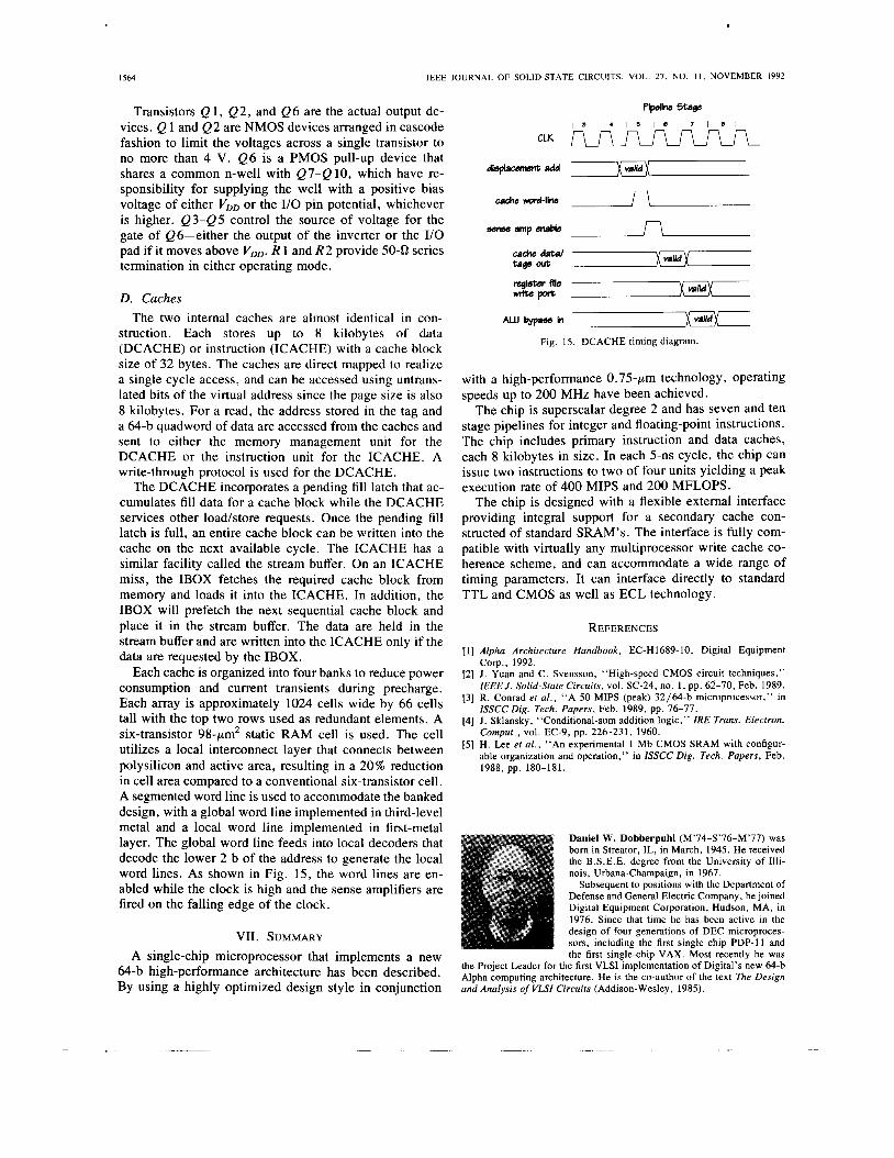
Each cache is organized into four banks to reduce power consumption and current transients during precharge. Each array is approximately 1024 cells wide by 66 cells tall with the top two rows used as redundant elements. A six-transistor 98-pm2 static RAM cell is used. The cell utilizes a local interconnect layer that connects between polysilicon and active area, resulting in a 20% reduction in cell area compared to a conventional six-transistor cell. A segmented word line is used to accommodate the banked design, with a global word line implemented in third-level metal and a local word line implemented in first-metal layer. The global word line feeds into local decoders that decode the lower 2 b of the address to generate the local word lines. As shown in Fig. 15, the word lines are en- abled while the clock is high and the sense amplifiers are fired on the falling edge of the clock.
VII. SUMMARY A single-chip microprocessor that implements a new
64-b high-performance architecture has been described. By using a highly optimized design style in conjunction
with a high-performance 0.75-pm technology, operating speeds up to 200 MHz have been achieved.
The chip is superscalar degree 2 and has seven and ten stage pipelines for integer and floating-point instructions. The chip includes primary instruction and data caches, each 8 kilobytes in size. In each 5-11s cycle, the chip can issue two instructions to two of four units yielding a peak execution rate of 400 MIPS and 200 MFLOPS.
The chip is designed with a flexible external interface providing integral support for a secondary cache con- structed of standard SRAM’s. The interface is fully com- patible with virtually any multiprocessor write cache co- herence scheme, and can accommodate a wide range of timing parameters. It can interface directly to standard TTL and CMOS as well as ECL technology.
REFERENCES
[ 11 Alpha Architecture Handbook, EC-H1689-10, Digital Equipment Corp., 1992.
[2] J . Yuan and C. Svensson, “High-speed CMOS circuit techniques,” IEEEJ. Solid-State Circuits, vol. SC-24, no. 1 , pp. 62-70, Feb. 1989.
[3] R. Conrad et a l . , “A 50 MIPS (peak) 32/64-b microprocessor,” in ISSCC Dig. Tech. Papers, Feb. 1989, pp. 76-17.
[4] J. Sklansky, “Conditional-sum addition logic,” IRE Trans. Electron. Comput., vol. EC-9, pp. 226-231, 1960.
[5] H. Lee et a l . , “An experimental 1 Mb CMOS SRAM with configur- able organization and operation,” in ISSCC Dig. Tech. Papers, Feb. 1988, pp. 180-181.
Daniel W. Dobberpuhl (M974-S’76-M’77) was born in Streator, IL, in March, 1945. He received the B S.E.E. degree from the University of 1111- nois, Urbana-Champaign, in 1967.
Subsequent to positions with the Department of Defense and General Electric Company, he joined Digital Equipment Corporation, Hudson, MA, in 1976. Since that time he has been active in the design of four generations of DEC microproces- sors, including the first single chip PDP-11 and the first single-chip VAX. Most recently he was
the Project Leader for the first VLSI implementation of Digital’s new 64-b Alpha computing architecture. He is the co-author of the text The Design and Analysis of VLSI Circuits (Addison-Wesley, 1985).
- .-

1565 DOBBERPUHL et al.: 200-MHz 64-b DUAL-ISSUE CMOS MICROPROCESSOR
Richard T. Witek received the B.A. degree in computer science from Aurora College, Aurora, IL, in 1977.
He joined Digital Equipment Corporation, Hudson, MA, in 1977, working on Phase 2 DEC- net. In 1982 he joined the Digital VLSI group. In the VLSI group he worked on CAD development, MicroVAX VLSI chips, and a variety of intemal RISC projects. He was a co-designer of the Alpha architecture, and the principal microarchitect of the EV-4 CPU chip. He is currently with Apple
Computer, Inc. in Austin, TX.
Randy Allmon received the B.S. degree in elec- trical engineering from the University of Cincin- nati, Cincinnati, OH, in 1981.
He joined the Semiconductor Engineering Group at Digital Equipment Corporation, Hud- son, MA, as a circuit designer following gradua- tion. He has contributed to the development of nu- merous VAX and Alpha high-performance CMOS processors. Currently he is responsible for the technical design and management of a next-gen- eration Alpha processor. He is the co-author of
four high-performance processor papers given at ISSCC and has one patent pending.
Robert Anglin was bom in New York, NY, on September 3, 1965. He received the S.B. and S.M. degrees in electrical engineering in 1989 from the Massachusetts Institute of Technology, Cam- bridge.
In the same year he joined Digital Equipment Corporation in Hudson, MA, where he has since worked on the design of high-performance micro- processors.
Mr. Anglin is a member of Sigma Xi.
David Bertucci received the B.S.E.E. degree in 1982 from Wayne State University, Detroit, MI, and the M.S.E.E. degree in 1988 from Michigan State University, East Lansing.
He joined Digital Equipment Corporation, Hudson, MA, in 1989 where he worked on advanced CMOS microprocessor design. Currently he is em- ployed at Sun Microsystems Inc., Mountain View, CA.
Linda Chao (M’88) received the B.S.E.E. degree from the Massachusetts Institute of Technology, Cambridge, in 1987. She is currently pursuing master’s degrees in electrical engineering and management through the M.I.T. Leaders for Manufacturing Program.
Since joining Digital Equipment Corporation, Hudson, MA, in the Semiconductor Engineering Group/Advanced Development in 1987, she has been engaged in the design of full-custom VLSI microprocessors.
Robert A. Conrad received the B.S. degree in electrical and computer engineering from the Uni- versity of Cincinnati, Cincinnati, OH, in 1984, and the M.S. degree in electrical and computer engineering from the University of Massachusetts at Amherst in 1992, where his thesis was entitled, “MPPE: A Multiport Data Driven Processing Element.”
In 1981 he joined the Semiconductor Engineer- ing Group of Digital Equipment Corporation, Hudson, MA, where he worked as a co-op in the
Architecturally Focused Logic group. Since 1984 he has been engaged in the research and development of VLSI microprocessors, including Digi- tal’s MicroVAX CPU (1984), a 50-MHz RISC CPU (1989), and most re- cently Digital’s Alpha chip.
Daniel E. Dever received the B.S.E.E. degree in 1988 from the University of Cincinnati, Cincin- nati, OH.
He joined the Semiconductor Engineering Group of Digital Equipment Corporation, Hud- son, MA, in 1988, where he worked on the design and logic verification of CMOS VAX micropro- cessors. Since 1990 he has been involved in the design of RISC architecture microprocessors, in- cluding the floating-point unit of the 21064. He is currently involved in the design of integer arith-
metic logic for the next-generation Alpha processor.
Bruce Gieseke was bom in Mason, OH, on Sep- tember 16, 1959. He received the B.S. degree in electrical engineering from the University of Cin- cinnati, Cincinnati, OH, in 1984 and the M.S. de- gree in electrical engineering from North Carolina State University, Raleigh, in 1985.
In 1986 he joined the Semiconductor Engineer- ing Group, Digital Equipment Corporation, Hud- son, MA, where he has been engaged in the im- plementation and circuit design of RISC microprocessors.
Soha M. N. Hassoun received the B.S.E.E. de- Sharon Britton received the B.S.E E. degree gree from South Dakota State University, Brook- from Boston University, Boston, MA, and the ings, in 1986, and the S.M.E.E. degree from the M.S.E.E. degree from Massachusetts Institute of Massachusetts Institute of Technology, Cam- Technology, Cambndge, in 1983 and 1990, re- bridge, in 1988. Since October 1991 she has been spectively. a student at the University of Washington, Seat-
She joined Digital Equipment Corporation, tle, Computer Systems Engineenng Department, Hudson, MA, in 1983, where she worked on the pursuing a Ph.D. degree. design and development of 801 86-based control- From August 1988 to August 1991 she was em- lers for read-only and write-once optical disk ployed at Digital Equipment Corporation, Hud- dnves. From 1987 to 1989 she attended M.I.T. as son, MA, as a Custom Design Engineer In the part of Digital’s Graduate Engineering Education Semiconductor Engineering Group. She contnbuted to the design of the
Program. Her graduate research involved the development of an integrated floating-point unit of the 21064 processor. content addressable memory system with error detection capability. She Ms. Hassoun was the recipient of a Digital’s Minonty and Women’s returned to Digital in 1990 to join the Semiconductor Engineering Group, Scholarship in 1991. She was a Tau Beta Pi Fellow in 1986-1987. She was where she is involved in the design and implementation of high-perform- selected as the most outstanding senior in the College of Engineering in ance CMOS microprocessors. 1986.

1566
Gregory W. Hoeppner (S’79-M’81) graduated with distinction from Purdue University, West Lafayette, IN, in 1979 where his research topic was ion-implanted optical waveguides.
In 1980 he worked at General Telephone and Electronics Research Laboratory, Waltham, MA, performing basic properties research on GaAs for fabrication of submicrometer FET’s. From 1981 to 1992 he held a number of positions with Digital Equipment Corporation, Hudson, MA, most re- cently as co-implementation leader of Digital’s
IEEE JOURNAL OF SOLID-STATE CIRCUITS, VOL. 27, NO. I I , NOVEMBER 1992
Alpha chip. He is currently employed a i a Senior Engineer at IBM, Ad- vanced Workstation Division, Austin, TX.
Kathryn Kuchler (S’89-M’90) received the B.S. degree in electrical engineering from Cornell Uni- versity, Ithaca, NY, in 1990.
Upon graduation she joined Digital Equipment Corporation in Hudson, MA, where she has worked on the first implementation RISC micro- processor based on the Alpha architecture.
Maureen Ladd (S’85-M’86) received the B.S. degree in computer engineering from the Univer- sity of Illinois at Urbana-Champaign in 1986.
Upon graduation she joined the Semiconductor Engineering Group within Digital Equipment Corporation, Hudson, MA, and worked on a 32-b RISC microprocessor. She received the M.S.E. degree in electrical engineering from the Univer- sity of Michigan in 1990 through Digital’s Grad- uate Engineering Education Program. Upon her return to Digital, she worked on the implementa-
tion of the first Alpha microprocessor.
Burton M. Leary received the B.S.E.E. degree from the University of Massachusetts at Amherst in 1980.
He joined Digital Equipment Corporation, Hudson, MA, in 1980 and is currently a consult- ing engineer in the Semiconductor Engineering Group/Advanced Development Memory Group. He designed the instruction and data caches for the Alpha CPU and is currently working on the design of advanced memory products.
Liam Madden was bom in Waterford, Ireland, on June 1, 1958. He received the B.S. degree from University College Dublin, Ireland, in 1979 and the M.E. degree from Cornell University, Ithaca, NY, in 1990.
From 1979 to 1981 he designed industrial mi- cro-controllers for Mahon and McPhillips, Ire- land. From 1981 to 1984 he worked for Hams Semiconductor, Melbourne, FL, where he con- tributed to the design of CMOS microprocessor peripherals. He joined Digital Equipment Corpo-
ration, Hudson, MA, in 1984 and has since designed both CISC and RISC microprocessors and contributed in the area of CMOS process develop- ment. He is currently a Consultant Engineer in a CPU Advanced Devel- opment group and his interests include circuit design and CMOS technol- ogy development.
Edward J. McLellan was born in Providence, RI, on April 15, 1958. He received the B.S. degree in computer and systems engineering from Rensse- laer Polytechnic Institute, Troy, NY, in 1980 where he was elected to Eta Kappa Nu.
He joined Digital Equipment Corporation, Hudson, MA, in 1980 and contributed to the de- sign of several processor chips. He holds three patents in computer design and has an application pending.
Derrick R. Meyer was bom in LaGrange, IL, on November 24, 1961. He received the B.S. degree in computer engineering from the University of Illinois, Urbana, in 1983.
In 1983 he joined the embedded controller group of Intel Corporation in Chandler, AZ, where he was involved in the design of various CMOS mi- crocontrollers, including the 80C51 and 80C196. In 1986 he joined the Semiconductor Engineering Group of Digital Equipment Corporation in Hud- son, MA, where he was initially involved in the
design of the cache and memory systems for a chilled CMOS VAX pro- cessor. He has been involved in the development of Digital’s Alpha mi- croprocessors since 1988.
James Montanaro received the B.S.E.E. and M.S.E.E. degrees from the Massachusetts Insti- tute of Technology, Cambridge, in 1980.
He has been with Digital Equipment Corpora- tion, Hudson, MA, since 1982. He was a circuit designer on the floating-point chip for the LSI 11/ 74 and a MicroVAX peripheral chip and he led the physical implementation of the uPRISM CPU, a 70-MHz prototype RISC CPU completed in 1988. As one of the technical leaders of the Alpha CPU chip project, he led the physical implementation
of EV-3, the first Alpha CPU chip, and then contributed as a circuit de- signer on the EV-4 design.
Donald A. Priore received the S.M. degree in electrical engineering and computer science from Massachusetts Institute of Technology, Cam- bridge, in 1984.
In 1984 he joined Digital Equipment Corpora- tion, at their Hudson, MA, semiconductor design and manufacturing facility, working initially on device characterization, yield enhancement, and yield modeling of NMOS and CMOS processes in manufacturing. Subsequently, he joined a CMOS design group, working first with low-temperature
CMOS technology, and later with conventional CMOS in high-perfor- mance microprocessor design. His interests have included signal, clock, and power integrity in the on-chip environment. He is presently a Principle Engineer working on CMOS chip design.
Vidya Rajagopalan received the B.E. degree in electronics engineering from Visvesvaraya Re- gional College of Engineering, Nagpur, India, in 1986, and the M.S. degree in electrical engineer- ing from the University of Maryland at College Park in 1989.
She was with Norsk Data India Ltd. from 1986 to 1987 as a Systems Design Engineer. In 1989 she joined the Semiconductor Engineering Group of Digital Equipment Corporation, Hudson, MA, and was on the design team of the 21064 RISC

I I
DOBBERPUHL et al.: 200-MHz 64-b DUAL-ISSUE CMOS MICROPROCESSOR I567
microprocessor. She is mance microprocessors
currently involved in the design of high-perfor- at Digital.
Sridhar Samudrala received the M.Sc. (Tech) degree from Andhra University, India and the M.S.E.E. degree from the University of Wiscon- sin, Madison.
He is currently a Project Leader for the devel- opment of a CMOS microprocessor chip at Digital Equipment Corporation, Hudson, MA, in the Semiconductor Engineering Group. He joined Digital in 1977.
Sribalan Santhanam received the B.E. degree in electrical engineering in 1987 from Anna Univer- sity, Madras, India, and the M.S.E. degree in computer science and engineering in 1989 from the University of Michigan, Ann Arbor.
In 1989 he joined Digital Equipment Corpora- tion, Hudson, MA as a Design Engineer for the Semiconductor Engineering Group, responsible for the full-custom design and development of high-performance CMOS VLSI processors. He worked on the design of the floating-point unit of
the 21064 processor including the double-precision multiplier. He is cur- rently involved in the design of another high-performance RISC processor.