A 13cm GaAsFET Power Amplifier Developed Using the PUFF CAD Software Package
12
VHF COMMUNICATIONS 3/94 --------- - --'-'-"--""'"''-'''= -''=''-=' Harald Fleckner, DeB UG A 13cm GaAsFET Power Amplifier Developed using the 'PUFF' CAD Software Package Trausl srorl scd power ampttrters for the fr equency ran ge between and 2,400 MII z have fr eque ntl y been de scr ibed in r ecen t ye a rs . (1)(2)(3)(4)(5)(11) The z-stagc power aurpttrlcr in- troduced here supplies un initial out- put of 5 Watts at 23 dB amplifleatlon in the Bem blind. l. INTROD UCTI ON The goul of the project was to develop several amplifiers using the software, build them, and compa re the readings with th e simulated values. Three diffe rent typ es of amplifier were in- vo lvcd in this project, with different performance figures varying from 4 to 12 Watts in the given frequency range. The following article describes the selection of semi-conductors. the sim- ulafion/analysis of the amplifier circuit using the CAll software, the building of the 5 Wall amplifier and the readings obtain ed. The circuit was developed using the pun; CAD software package, which makes it ama zingly simple to calculate and simulate even relatively compli- cared microwave circuits. Several publi- cations (7)(8), together with our own research, have already put the capabil- ity of the low-cost soft ware used to the test, so that very positive results were to be expected. 2. SELECTING SEMI- CONDUCTORS The transistors use d in the amplifier were Mit subis hi type, from the 0900 range for UHP power amplifiers. 1bey were, in actual fact, N-channel Schottky 130
-
Upload
anon849270 -
Category
Documents
-
view
26 -
download
5
description
.
Transcript of A 13cm GaAsFET Power Amplifier Developed Using the PUFF CAD Software Package
VHF COMMUNICATIONS 3/94(~,---------- --'-'-"--""''"''-'''= -''=''-='
Harald Fleckner, DeB UG
A 13cm GaAsFET PowerAmplifier Developed using the'PUFF' CAD Software Package
Trauslsrorlscd power ampttrters forthe fr equency range between 2,~O()
and 2,400 MIIz have fr eque ntl y beend e scr ibed i n r ecen t ye a rs .(1)(2 )(3)(4)(5)(11)
The z-stagc power aurpttrlcr introduced here supplies un initial output of 5 Watts at 23 dB am plifleatlonin the Bem blind .
l.INTROD UCTION
The goul of the project was to developseveral a mplifiers using the software,build them, and compare the readingswith th e simulated values. Threediffe rent types of ampli fier were invo lvcd in this project, with differentperformance figures varying from 4 to12 Watts in the given freque ncy range.
The following art icle describes theselection of sem i-con ductors. the simulafion/analysis of the am plifier circuitusing the CAll so ftware, the building ofthe 5 Wall amp lifier and the read ingsobtain ed.
The circuit was developed using thepun; CA D software package, whichmakes it ama zing ly simple to calculateand simulate even relatively complicared microwave circuits . Several publica tions (7) (8) , together with our ownresearch, have already put the capability of the low-cost software used to thetest, so that very positive results wereto be expected.
2.SELECTING SEMICONDUCTORS
The transistors used in the amplifierwere Mit subishi type, from the 0900range for UHP power amplifiers. 1b eywere, in actual fact , N-channel Schottky
130
=-===""""'-"''''------- ---- (¥'VHF COMr'.1UNICATIONS3/94
fPo ints ~~8 PLOT
S~ith radius 1t Z .32lh GHz
[]Sl1 -za.zaaa 93 .7 ·x SZl 2"."7"3<IB 17i.9·
S12 - 35 . 2 8<111 110> ,9·+= - 33 . 5" d ll 1Z1.h·
_ H U1I'OUT _
f il n
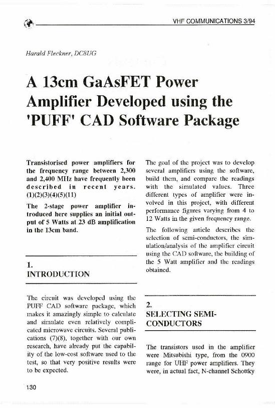
Fi~ . l: Screen Dump from the PUFF CAD Pa ckage
Amplifi cation:Outpu t:
(jaA ~ power rE T' s. which had alreadybeen successfully used in the construet ion of several circuits (6)(11), andwhich could he obtained at relativelylow cost. Their power spectrum stretched from O.6W (the 0904 type) rightup to lOW (the 0907 type) for amplification levels of between Rand 13dB.depend ing on type and frequency .
TIle performance Figures targeted hy thedeve lopm ent:
> 20dB atk > 1min5W atmax IdB compression
Band width: HX) MHzZ;n = 7-'{>ut = 50n at return loss ? 20dB
The type 0906 seemed a suitable highlevel stage trans istor. It display ed part icular ly hig.h operational thermal stability because of its large ceramalhousing and, in contrast to the 0905,which was usually running under strain,easily supplied 37dHm = 5W at 1dBcompression, thus guarantee ing stableoperation with permanent output - e.g.for ATV transmitters. The type 0904was a suitable driving transistor, because it displayed a high level ofamplification (l3 dB) for a compressionfree output amounting to almost 2RdBm= 630mW. The Scparameters of theselected tra nsistors required for thedevelopment of {he circuit came fromthe Mirsubishi data hank, and appli edunder the following DC conditions:
could therefore be attained only with az-stage amplifier.
MGF0904 : UDS =9 V at ID =0.2 A
MGF0906: UDS = 10 V at ID = 1.1 A
131
VHF COM MUNICATIONS 3194(/'0----------~~~=~~~
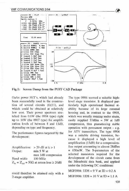
•••••• - ~ - --- -~-IT r Qb •FI~. 2: Frequenc,' pi...... or II Circuit ror the 9cm ba nd
Tbc ef ficiency o f these tr:lIl~i"lon wasnorm ally about -ll)';; . so thai 3 OC inpmpower of more than 12 wau s wasrequired in operation. and lhe re..ultingpower loss had to he dissipated througha heat sink of sufficiently large dimensions .
3.SI\IULATlON A:\J)ANALYSIS OF A~IPLIFIER
CIRCUIT CSI:'/C; CADSCWrWARE
"Inc method of functioning and theopera tion of the PCI-l; CAD softwarearc com prcbcnstvc ty described in(7)(R)(Q). so here we sha ll mere ly listand anal y..c the results obtained.
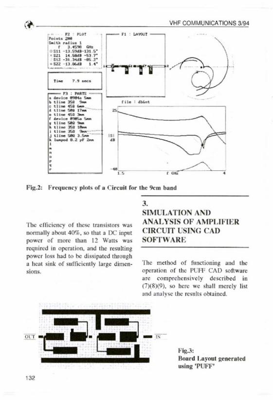
Fl~_':
Board Le yout genera tedU"inll 'PUFF'
132
VHF COMMUNICATIONS3/94
,
I ~,.-",,,..
I ,,.-vs...I- .',I, I ' I",. , ->C"'. . , ••-.,." , ... , •. " " " ••
I I I ' ~h-, " " . ' "' j
, " - - ' - - - 0 ' " r'", '_' _ ..loi.__ .~ ..-f-----. - ... _ .:. . "",.. " "l
0 _ 'V_ o _ ,", _ " " . '" t-, " . " '" ""1 ,~ ,, d o' ,," " '1" " .,,, IL }- ., ( . L
I J c ~ C~ R 5 - F ~ , -P A
P '1 13 - 5 ~ u t tDCSU(j
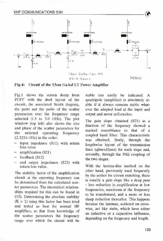
Fig.4: Circuit of the Belli GaAs F ET Power Amplifier
Fi g.I shows the screen dump frompurr- with the dra ft layout of thecirc uit, the assoc iated Smith diagram .the par ts and the path s of the scatterparameters over the frequency rangeselected (1.5 to 3.0 (JIIz). The plotwindow (top left ) al so shows the sizeand phase of the scatte r param eter s forthe selected ope rat ing frequenc y(2.321 6 Gl lz) in the order:
input impedance (Sl l ) with rerumloss value
am plificetion (S21)fee dback (S12)
and output impedance (S22) withreturn loss value.
The stability factor of the amplificationcircuit at the operating frequency canhe determined from the calculated scattcr para meters. The theoretical relationships required for this can he found in(10). Determining the abso lute stability(K > 1) using this factor has been triedand tested as best for normal HFampl ifiers, so that from knowledge ofthe scatter parameters the frequencyrange over which the circuit will be
stable can easily be indicated. Aqnadri polc (am plifier) is absolutely stable if it a lways remains stable whatever the adapted load at the input andoutput and never sel f-excites.
The gain slope obtained (S2l) as afunction of the frequency showed amarked resemblance to tha t of acoupled band filter. This characteristicwas obtained, firstly, through thelengt hwise layout of the transmissionlines (ql incs/tline s) for each stage and,secondly, through the son coup ling ofthe two stages.
With the lamina-disc method on theother hand, previously used frequentlyhy the author for circuit matching, thereis usually a gain slope like a deep pass- less reduction in amplification at lowfrequencies , maximum at the frequencyto be transformed, and a more or lesssharp redaction thereafter. This happensbecause the laminae, soldered on crosswise, act like stubs, which 11:lVe eitheran inductive or a capacitive influenc e.depending on the frequency and length.
133
(~ VHF COMMUNICATIONS 3/94
NAME TYPE VALUE STYLE COM~IE:-ITS
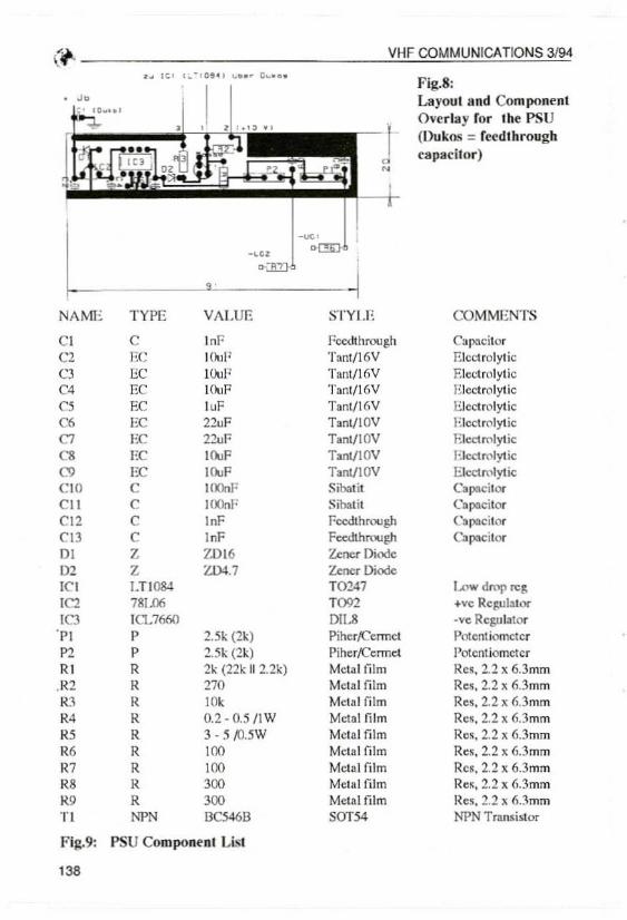
CI TC 2.5pf Te flonC eramic Tri mmerC2 TC 2.5pf Teflon.Ceramic Tri mmerC3 TC :?:.5pf Teflon.Ceramic Tri mmerC4 TC 2.5pt Teflon.Cera mic Tri mme rC5 C l Op! Tekelec-Cbip Capacito rC6 C 4.7pF ATC.Chip Capac itor<..'7 C 4.7pF ATC-Chip Ca pacitor11 r; N-Connedor12 r; N·Connec torL1 11. Zs= lOO124mm Striplinc Trans-LineL2 11. 1.5= lOO{.!4mm Strip linc Trans-LineL3 11. "Zs= lOO124mm Srnplinc Trans-LineIA TL 7.s= 70/24mm Striplinc Trans-LineTI fo11T 0904 Mitsubishi N-GaAsPETT2 fo11T 0906 Mirsubi shi N-GaAsFETZS 11. Zs'" 22/2.lmm Stripline T rans-l .inc2 1 11. Z= 161l6ml1l Stripline Trans-Line7.2 TI. '1..= 25/1 :'imm Strip line T rans-Line7.3 11. '1.= 16/16mm Striplinc Trans-Line7A TL Z= 2216Jmm Striplinc Trans-Line
Fill..:>: Component List for the Amplilicr
To male this d earer. Fig.2 shows thesimulated frequency response curve inaccordance with a circui t published in(6) for the 9c m hand. with 0004 and0905 tran sistors. without OC choking.With !i.li~ht modifications to the circuit,th is amplifier can also he operated at13cm without prob lems. as shown by anankle in (11). though of course atconsiderably Jess than 2OdO amplifica tion.
The read ings shown in Fig. l gave thefollowin g output va lues for the dra ftcircuit:
Re turn loss input; -23dB
Return loss output: -33dBAmplification at 2,320 MHz: 24.8dBFeedback: -35dBK-factor at 2.320 .MHz; 5
134
Band width (-JdO): -280/+120 Mill
Fig.3 shows the layout generated by theCA D software as 3 print-out from alaser printer for Teflon-based materialwith a substrate thickness of O.79m m.The subsequent introd uction of acorrection factor 10 generate a precisephotographic model is thus poss ible.The revers ed image is pictured. asgenerated on the exposed board.
T he tracks on the longitudina l boardside arc earth surfaces inserted subsequently , which arc throu gh-holeplated to the earth surface when thecirc uit is assem bled.
In the parts list in Fig. f , we can a lsorecognise the discrete modules requiredfor the circuit under the description of
VHF COMMUNICATlONS 3/94
,~
~6.5 • 1.5
!'lI'lJI
!~".,hch,"~l a <11"'"
1\1.. ~"" 1<61p<w! 10 . 100. ,O
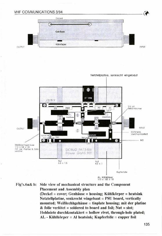
FiJ;:'s.6a& b: Side view of mech anica l structure and the ComponentPlacement and Assembly plan(Deckcl ;; cover, Genha usc ;; housing: KfJhlkorper ;; hcatsinkNctztettplatlne, scnkrecht wingcbaut ;; PSlJ board, vcr tlcettymounted ; wctmcchhge hause = tinplate housi ng: mil der plaline& rolic v('r llite l ;;: soldered to board a nd roil; "'ul = slol;lIohlnlele du rchkont ak lert ;; hollow river, throu gb-hclc plated ;AL· Kuhlkor per =AI heat sink : Kup ferfolle =cop per roil
135

VHF COMMUNICATIONS 3/94(~, --'-"'--""'==c:.=:=" lumpe d". These arc capacitors andresistances which life required for thecircuit 10 operate. In this connection.Fig.a shows the IIF circuit diagram andPig .S the parts list.
4.ASSEMBLING TI lEAMPLIFIER
Th e amplifier c ircu it was built on aTeflon board (cr = 2.31) with dimensions of \09 x 54 x 0.79 (mm) For itspart, it was screwed to an aluminiumcooling body (110 x 100 x IOm m),whic h was used for fa~kning and as aheat sink for the power transistors andvoltage controllers (Fig.6),
The use of epoxy resin based materialwas excluded. since power amplifiers inthis range alread y produce dielectriclosses of 2CYJ, (app. l dB ), i.e. a loss of1W at 5 Wens ruuput .
So. co mpared with the costs of thetrans istors (app. DM 60/Wau), it wouldhe a fa lse economy.
The Ix.:: power supply system wasassembled on an epo xy board, coaledon both sides (9 1 x 20 x 1.6mm), whichwas vert ica lly solde red to theIongnudina l side of the housing (Fig.o)within. Its c ircuit corresponded to theone published in (6).
rigs. 7. 8 and 9 show the screen. layoutand parts list for this power supply. Thecomponent s tire mounted 0 11 the foilside, so that the earth surfaces have tobe through-hole plated .
Grooves were milled in the heat sink sothat the drain and gate connections ofthe transistors could be soldered flushto the board. as far as possible. For thispurpose, the Teflon board had recessesmeasuring 4.4 x 17 (mm) and 6.4 x 22(rnm), into which the transistors wereinserted and then screwed to the heatsink (see Fig.6). There was also acopper foil between the hoard and theheat sink (115 x 57 x O.OSlIIlIl), whichwas later soldered to the tinplate housing. It prov ided a vel)' good earthcon nection between the transistors, theboard, the housing and the heat sink.
Before the board was mounted , theearth surfa ces had to be through-holeplated with 2mm copper (hollow)rivets. At least 4 rivets per longitudinalside and earth con nector arc requiredfor this (see Hg.6).
The hoard was fastened to the heat sinkat 6 points. using M2 screws. Thetransistors each required 2 threadedholes in the basepla te for the sourceconnection, which were best provided,true to dimensions. with the help of apiece of cardboard which correspondedto the transistor dimensions.
The dimensions of the tinplate housin gwere I to x 55 x 28 (mm) and beforeassembly it was provided with thenecessary bores (or the feedthroughcapacitors and recesses (or the N·sockets. The housing itself was thensoldered together. and soldered to thelongitudinal sides of the screwed-onboard. The soldered-on sockets couldthen be screwed to the heat sinks on thefront (aces as well.
The best insertion and commissioningprocedure is as follows:
136
~~~"""'''''''''''''-''------------(t'VHF COMMUNICATIONS 3/94
i ,
,>.
-Q1--1
,I
,-..:;':
",:: :5.-
I
,crn. 0I c
e -rW o
u, ,I C, m
IT l, a ,co ,
EE 0U t
en ,uc
.~
t
, ,
-1]1-- - ,
, '> ", ,·,., '·,,"• •~ ~,,
•,
"- ,.-:1
,
ir~ 10; I
I c, ,I " u, . -
'L " ·DI--1 ji
..-J~--'--- - - ....+1~
>
_ ---1'>-,I
~; ~ J ;;" ,-- ' -"
' -
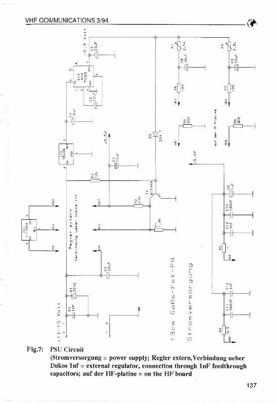
Fig.7: PS U Circuit(Stromvcrsorgung e power supply; Regier cxtern.verbtndung ueberDukos lnf :;:; external regulator, connection through InF feedthroug hcapacitors: auf der IIF-pla tine = on the flF hoard
137
VHF COMMUNICATIONS 3194(~--- - - - ---'-'-"-'=""'""""""'=
COMMENTS
Fi~.8:
Layout a nd ComponentO ver tay ror the PSUIUu"-ns = recdthrougbca pac itor)
STY I.E
o:B1)-
VALUE
.1 .I J." ..
TYPE
I-----'~. ---~
. '", . 'O w• • ,
ClC2CJC4rlCoc:C8f9CIOellenCI3J)J
IJ2ICI1C210PIP1RI
.R2
" J"4" 5"6"7"8".TI
cFeECECECECECECEccccczZ1.1 1084781.0610 .7660PPR
"RR
"RRR
"NPN
InF1(~ 1 ]i
l l\IF101iFI,F2:!1.IF221JFI,,"FI,,"FIl..lnl'iliOnI'InFInF7J>l6Zl.>4.7
25k (2k)2.5k (21;)2k (22k II l .2k)27010kO.2 - 0.5 /lW3· .'i /O.5W100100300300DC546D
I 'ccdthrou ghT anl/ 16VTanl/ 16VTanl/16VTanl/16VTanl/ IOVrant/I OVTant/IOVTant/lOVSihat itSihalitFccdth r\lllghFcethhn'lPJZener l)i,'deZener Diode10247TOQ2DII.8Pihcr,K'ermc:tPihc: rK'cnnelMetal filmMctal lilmMetal FilmMctal lilmMl'Ial filmMetal filmMet al filmMctalIllrnMetal filmSOT'"
Cap;lc itllrElectrolytic
Electrolyticlqcct rolyt lc
Elect rolyticElect rolyticElectrolyticFled wty! icElect11\1)1icClipacill¥Ca~C il(lf
CepecuorCapacilt¥
I .('W drnp n:~
+vc Rcp llah¥-ve Regulator
Pot ent iom ctcrI'otcnnomctcrRes, 2.2 x 6.3mmRu , 2.2 x 6.3mmRe s, 2,2 x 6.3mmRes, 2.2 x 6.3mmRes , 2.2 x 6.3mmRes , 2.2 x 6.3mmRes. 2.2 x 6.3mmRes, 2.2 x 6.3mmRes, 2.2 x 6.J mmNP N T ransistor
Ftj;!;.9: PSU Com ponent List
138

"-"-"""""""= -'-"""'-"'-""---- - - - --- - - - (f':VHF CO MM UNICATIONS 3/94
Assemble and moun t power supplyboa rdGate resistances (R6. R7) should already be soldered onto power supplyfor better mount ing (sec Pig .S)!
A ss emble and wire up the 6 feedthrough capacitors ( InF ) and the blocking capacitors C3. C5, CIO. CI Ifasten (insulurionl ) and connect upvoltage controller by me ans offeed through capacitorsMount and co nnect up resi stances(R4 . R5, R8. R9) to and on IIFboardMo u n! trimmers (C I . C2. C3 , ( 4)
MOUll! chip capacitors (C5. C6, C7 )
The power supply (UG and D) cannow be te sted.
Mo un! GaAsFET's
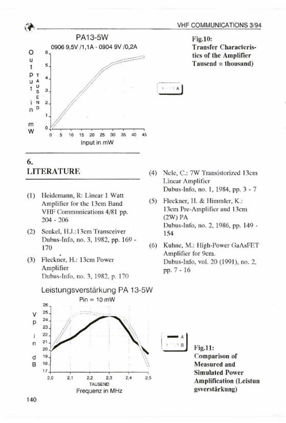
Fig. l O shows the transfer cha racteristicof the amplifier.
At 5 Watts output, the compressionrange begins, i.e. a furt her increase inpo wer lead s to a consider ableworsening of the inter-modulation interval; (l dR compression a -33dBin ) .
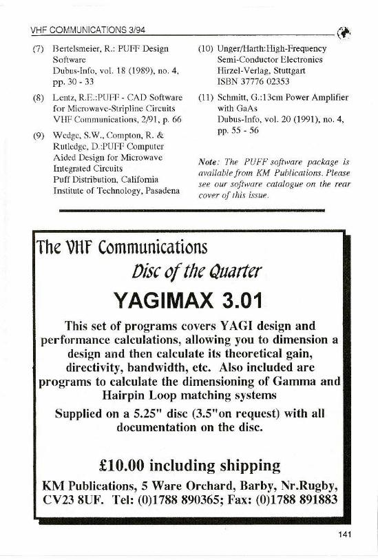
f ig.I I shows the power amplific ation atan input 10mW over the frequencyrange.
Curve 1\ shows the measured gradientarising if the amplifier is tuned to 2,320MHz.
Curve B shows the grad ient obtai nedthrongh simulation. in accordance withFig .l .
The st atic current lev els can now beset :
0904 • In =0.21\ ; WOo - lD =l.lA
Note : for continuous operation in unfavoura ble conditions. it is advisable tomo unt the amplifier on an addit ionalheat s ink (c.g the housing wall), toensure stable operation.
5.READINGS
The p rototype amplifier was constmcted so that a 5 Watt output coul d beachieve d with an input of 28mW at2.320 MHz. The measurement wascarried out using a type HP 432Wattm eter and a 30dB attcnua tor fromNarda.
Con seque ntly, the ampli fier has a handwidth of 300 MI [z. Its ampli ficat ionreduction at the band limits is of coursesomewhat less than in curve n. Thereasons for this arc the losses conditi0 11:11 on the c ircuit, which can not becovered comp letely hy the simulation.
The linear amp lification of 2d13 obtaiucd is only slightly di fferent hom thecalculated value . If the amplifier isbroad -hand tuned. so that its coursecorresponds to curve S , the amp lification falls by about l dB (20'70) as theband width increases.
To sum up, we can say that using PUfflow-cost software to develop simpleintegrated high-frequency circu its canbe highly recommended. True. theef fic iency is very much reduced bycomparison with high-end productssuch as, for example, Super-Compact.but the results obtainable are more thanadequate for the amat eur sector.
139
VHF COMMUNICATIONS 3/94
Fi~ . I O :
Transfer Cheractcrtstics of the AmplifierTauscnd =thousand)
PA13-5W0906 9,SV11,l A - 0904 9V IO,2A,o
(/' - - ------ -------'-""-'''''-''''''''''''''''-''''''''''''''''
6.LITERATURE
( I) Itcidcmann. R: Linear 1 WaltAmplifier for the l Scm BandVIIF Com mnrnceuons 4/8 1 pp.204 - 206
(2) Scnkcr.Ll.r.i t xcrnTransceiverDubus-lnfc. no. 3. gnu. pp. 169 .170
(3) Hcckncr, H.: l Scm PowcrAmplifi erDubus-Iufo. no. J. 1QR 2. p. 170
(4) ~clc . Co : 7W Tranvietorized Lk lllLin ear AmplifierDubus-lnfo. no. I, 1984. pr . 3 - 7
(5) H eckner , II. & l l irnmlcr, K.:1Scm Pre-Amp lifier and l Jcm(2W) PI\.Dubus-lnfo. 110 . 2, 1986, pp. 149 ·154
(6) Kuhn e, Vi .: High-Power ( jaAsmTAmplificr for vern.Dubus-Into. vel. 20 (199 1). no. 2.pp. 7 • 16
t.eistunqsverstarkunq PA 13·5WPin :: 10 mW
zs
V " ---':._;.
p ..za
'~; za
I ,~ : Jn "ec , Fi~. 1 1 :d " 'i Co mpa rbon orB te Measured and
" Simulated Power'.0 .. u aa '.' z.s Amplification (Le ist un
TAUSEMJ
Frequenz in MHz ~'l " e r!'t a rkung)
140
VHF COMMUNICATIONS 3/94 '~========-- - - - --- - - - - - ,(7) Bertclsmeier, R.: PUFF Design
SoftwareDubus-Info. vo l. 18 (1989), no. 4,pp. 30 - 33
(8) L entz, R.E.:PUrr - CAD Softwarefo r 1vIlcrowavc-Striplinc Ci rcuitsV HF Communications, 2/9 1, p. 66
(9) Wedge, S.W., Compton, R. &Rut ledge, D.:l' UFF ComputerAide d Design for Microwav eInt egrated CircuitsP1.1ff Distribution, Ca liforniaIns titute of Technology, Pasadena
(10) Unger/H arth.High-PrequencySemi-C onductor ElectronicsHirzel-Verlag , StuttgartISBN 37776 02353
( II) Schmit t, G. : l 3cm Power Amp lifierwith GaA~Dubus -Info, vo l. 20 (1991), 110. 4,pp. 55 - 56
,Vote: The PUFF software package isavailable f rom KM Publications. Pleasesee our software catalogue on the rearcover of this issue.
The VHf CommunicationsDisc ofthe Quarter
YAGIMAX 3.01This set of programs covers YAGI design and
performance calculations, allowing you to dimension adesign and then calculate it, theoretical gain,directivity, bandwidth, etc. Also included arc
programs to calculate the dimensioning of Gamma andHairpin Loop matching systems
Supplied on a 5.25" disc (3.5" on request) with alldocumentation on the disc.
£10.00 including shippingKM Publications,S Ware Orchard, Barby, Nr.Rugby,CV23 8UF. Tel : (0)1788 89ll36S; Fax: (0)1788 891883
141