
A 10-Gb/s Monolithically Integrated Filterless … JOURNAL OF LIGHTWAVE TECHNOLOGY, VOL. 25, NO. 12,...
12
3748 JOURNAL OF LIGHTWAVE TECHNOLOGY, VOL. 25, NO. 12, DECEMBER 2007 A 10-Gb/s Monolithically Integrated Filterless InGaAsP/InP Widely Tunable Wavelength Converter With Conversion Gain Matthew N. Sysak, Member, IEEE, James W. Raring, Member, IEEE, Jonathon S. Barton, Member, IEEE, Henrik N. Poulsen, Daniel J. Blumenthal, Fellow, IEEE, and Larry A. Coldren, Fellow, IEEE Abstract—In this paper, we present the details of a mono- lithically integrated filterless wavelength converter based on photocurrent-driven technology. The device consists of an inte- grated tunable laser transmitter and an optical receiver. The trans- mitter includes a sampled-grating distributed-Bragg-reflector laser, an electroabsorption modulator, and a semiconductor op- tical amplifier. The optical receiver employs two semiconductor optical amplifiers and a quantum-well p-i-n photodetector. The wavelength converter is characterized at 10 Gb/s over a variety of bias conditions at various input-power levels in various digital- system experiments. Bit-error-rate measurements at 10 Gb/s over an output tuning range of 32 nm between 1531 and 1563 nm show power penalties less than 1 dB. Similar experiments over an input wavelength range of 25 nm from 1535 to 1560 nm show a power penalty less than 2.5 dB. For a wavelength conversion from 1548 nm to a range of output wavelengths between 1531 and 1563 nm, the facet-to-facet gain ranges from 9 to 13 dB, neglecting fiber coupling losses. Index Terms—Monolithic integrated circuits, optoelectronic devices, wavelength conversion, wavelength-division multiplexing. I. I NTRODUCTION A S BIT RATES and data-traffic levels scale in optical communication systems, dynamic wavelength manage- ment is viewed as critical to reduce blocking probabilities and provide an added flexibility to network architectures. Currently, dynamic wavelength switching is performed with the use of optical–electrical–optical (OEO) repeaters that are placed at high-traffic-network nodes. While these repeaters have been shown to be a viable solution at bit rates of up to 10 Gb/s and Manuscript received August 1, 2006; revised May 4, 2007. This work was supported in part by DARPA/MTO CS-WDM under Grant N66001-02-C-8026 and in part by Intel Corporation under Grant TXA001630000. M. N. Sysak is with the Ultrafast Optoelectronics Group, Department of Electrical and Computer Engineering, University of California—Santa Barbara, Santa Barbara, CA 93106 USA (e-mail: [email protected]). J. W. Raring was with the Department of Materials, University of California, Santa Barbara, CA 93106 USA. He is now with the RF/Optoelectronic Group, Sandia National Laboratories, Albuquerque, NM 87185 USA (e-mail: jarring@ engineering.ucsb.edu). J. S. Barton is with the Department of Materials, University of California, Santa Barbara, CA 93106 USA (e-mail: [email protected]). H. N. Poulsen is with the Optical Communications and Photonics Network Group, Department of Electrical and Computer Engineering, University of California—Santa Barbara, Santa Barbara, CA 93106 USA (e-mail: Henrik@ ece.ucsb.edu). D. J. Blumenthal and L. A. Coldren are with the Department of Electrical and Computer Engineering, University of California—Santa Barbara, Santa Barbara, CA 93106 USA (e-mail: [email protected]; [email protected]). Digital Object Identifier 10.1109/JLT.2007.909333 are currently moving toward 40 Gb/s, they suffer from a variety of drawbacks. Repeaters usually consist of several discrete components that have been copackaged together to perform wavelength management. Although this approach does allow for individual optimization of each discrete device, it suffers from inherent insertion-loss issues that occur when multiple components with different optimal optical-mode profiles are connected together. The narrow alignment tolerances that are created by these mismatched optical interfaces lead to complex packaging requirements that add cost and production time before the device can be brought to market. The other key drawback to the OEO repeaters is their inherent dependence on electronic circuit components. Particularly at high data rates, electronic circuit elements can be quite complex and require significant amounts of power [1]. As an alternative to using these OEO repeaters for wavelength-switching functionality, several monolithically integrated small-form-factor all-optical wavelength-switching elements have been proposed and demonstrated. Integrated devices that can combine several functionalities together on a single photonic chip offer significantly lower packaging costs with reduced power dissipation along with the potential for eliminating complex electronics. Examples of these integrated devices and the technologies that are utilized for wavelength switching include cross-gain and cross-phase modulation using optical amplifiers in interferometric structures [2], cross- absorption and photocurrent effects in electroabsorption mod- ulators (EAMs) [3], photocurrent-based optical gates [4], and wave-mixing approaches in fiber and optical amplifiers [5]. In the case of the photocurrent-based optical gates, excellent switching performance has been demonstrated with extinction ratios (ERs) in excess of 10 dB and bit rates of up to 500 Gb/s. Recently, several of these wavelength-switching elements have moved toward incorporating even more functionality onto a single small-form-factor device. Of particular interest in terms of adding new capabilities is an on-chip laser source [6]. Adding a laser to the integrated wavelength converter is attractive since it can reduce optical loss and potentially lower packaging costs. However, the integration of an on-chip laser source presents a new set of challenges. Previously, a filterless wavelength conversion using cross-absorption, cross-phase, and cross-gain effects simply mandated counterpropagating optical pump and data signals. With an integrated laser, this is more challenging since the stability of the optical source 0733-8724/$25.00 © 2007 IEEE
Transcript of A 10-Gb/s Monolithically Integrated Filterless … JOURNAL OF LIGHTWAVE TECHNOLOGY, VOL. 25, NO. 12,...

3748 JOURNAL OF LIGHTWAVE TECHNOLOGY, VOL. 25, NO. 12, DECEMBER 2007
A 10-Gb/s Monolithically Integrated FilterlessInGaAsP/InP Widely Tunable Wavelength Converter
With Conversion GainMatthew N. Sysak, Member, IEEE, James W. Raring, Member, IEEE, Jonathon S. Barton, Member, IEEE,
Henrik N. Poulsen, Daniel J. Blumenthal, Fellow, IEEE, and Larry A. Coldren, Fellow, IEEE
Abstract—In this paper, we present the details of a mono-lithically integrated filterless wavelength converter based onphotocurrent-driven technology. The device consists of an inte-grated tunable laser transmitter and an optical receiver. The trans-mitter includes a sampled-grating distributed-Bragg-reflectorlaser, an electroabsorption modulator, and a semiconductor op-tical amplifier. The optical receiver employs two semiconductoroptical amplifiers and a quantum-well p-i-n photodetector. Thewavelength converter is characterized at 10 Gb/s over a varietyof bias conditions at various input-power levels in various digital-system experiments. Bit-error-rate measurements at 10 Gb/s overan output tuning range of 32 nm between 1531 and 1563 nmshow power penalties less than 1 dB. Similar experiments overan input wavelength range of 25 nm from 1535 to 1560 nm showa power penalty less than 2.5 dB. For a wavelength conversionfrom 1548 nm to a range of output wavelengths between 1531 and1563 nm, the facet-to-facet gain ranges from 9 to 13 dB, neglectingfiber coupling losses.
Index Terms—Monolithic integrated circuits, optoelectronicdevices, wavelength conversion, wavelength-division multiplexing.
I. INTRODUCTION
A S BIT RATES and data-traffic levels scale in opticalcommunication systems, dynamic wavelength manage-
ment is viewed as critical to reduce blocking probabilities andprovide an added flexibility to network architectures. Currently,dynamic wavelength switching is performed with the use ofoptical–electrical–optical (OEO) repeaters that are placed athigh-traffic-network nodes. While these repeaters have beenshown to be a viable solution at bit rates of up to 10 Gb/s and
Manuscript received August 1, 2006; revised May 4, 2007. This work wassupported in part by DARPA/MTO CS-WDM under Grant N66001-02-C-8026and in part by Intel Corporation under Grant TXA001630000.
M. N. Sysak is with the Ultrafast Optoelectronics Group, Department ofElectrical and Computer Engineering, University of California—Santa Barbara,Santa Barbara, CA 93106 USA (e-mail: [email protected]).
J. W. Raring was with the Department of Materials, University of California,Santa Barbara, CA 93106 USA. He is now with the RF/Optoelectronic Group,Sandia National Laboratories, Albuquerque, NM 87185 USA (e-mail: [email protected]).
J. S. Barton is with the Department of Materials, University of California,Santa Barbara, CA 93106 USA (e-mail: [email protected]).
H. N. Poulsen is with the Optical Communications and Photonics NetworkGroup, Department of Electrical and Computer Engineering, University ofCalifornia—Santa Barbara, Santa Barbara, CA 93106 USA (e-mail: [email protected]).
D. J. Blumenthal and L. A. Coldren are with the Department of Electricaland Computer Engineering, University of California—Santa Barbara, SantaBarbara, CA 93106 USA (e-mail: [email protected]; [email protected]).
Digital Object Identifier 10.1109/JLT.2007.909333
are currently moving toward 40 Gb/s, they suffer from a varietyof drawbacks. Repeaters usually consist of several discretecomponents that have been copackaged together to performwavelength management. Although this approach does allowfor individual optimization of each discrete device, it suffersfrom inherent insertion-loss issues that occur when multiplecomponents with different optimal optical-mode profiles areconnected together. The narrow alignment tolerances that arecreated by these mismatched optical interfaces lead to complexpackaging requirements that add cost and production timebefore the device can be brought to market. The other keydrawback to the OEO repeaters is their inherent dependence onelectronic circuit components. Particularly at high data rates,electronic circuit elements can be quite complex and requiresignificant amounts of power [1].
As an alternative to using these OEO repeaters forwavelength-switching functionality, several monolithicallyintegrated small-form-factor all-optical wavelength-switchingelements have been proposed and demonstrated. Integrateddevices that can combine several functionalities together on asingle photonic chip offer significantly lower packaging costswith reduced power dissipation along with the potential foreliminating complex electronics. Examples of these integrateddevices and the technologies that are utilized for wavelengthswitching include cross-gain and cross-phase modulationusing optical amplifiers in interferometric structures [2], cross-absorption and photocurrent effects in electroabsorption mod-ulators (EAMs) [3], photocurrent-based optical gates [4], andwave-mixing approaches in fiber and optical amplifiers [5].In the case of the photocurrent-based optical gates, excellentswitching performance has been demonstrated with extinctionratios (ERs) in excess of 10 dB and bit rates of up to 500 Gb/s.
Recently, several of these wavelength-switching elementshave moved toward incorporating even more functionalityonto a single small-form-factor device. Of particular interestin terms of adding new capabilities is an on-chip laser source[6]. Adding a laser to the integrated wavelength converter isattractive since it can reduce optical loss and potentially lowerpackaging costs. However, the integration of an on-chip lasersource presents a new set of challenges. Previously, a filterlesswavelength conversion using cross-absorption, cross-phase,and cross-gain effects simply mandated counterpropagatingoptical pump and data signals. With an integrated laser, thisis more challenging since the stability of the optical source
0733-8724/$25.00 © 2007 IEEE

SYSAK et al.: INTEGRATED FILTERLESS WIDELY TUNABLE WAVELENGTH CONVERTER WITH CONVERSION GAIN 3749
requires tight control of any optical feedback. Several potentialsolutions to this issue have been proposed and demonstrated.These include cascaded wavelength converters, dual-order-mode approaches and multimode-interference (MMI)-basedfiltering [7], [8]. However, it has been difficult to demonstratea fully transparent single-stage solution due to optical beatingeffects between the on-chip pump and data signals whenwavelength switching is not desired [7].
As a solution to these filtering issues, a set of devices hasbeen demonstrated using a photocurrent-driven approach wherean on-chip optical receiver is used to drive a monolithicallyintegrated EAM and tunable laser [9]. Similar to the otherwavelength-conversion techniques, this device does not requireelectronics aside from a simple bias tee and a load resistor.However, the key benefit to this approach is that the opticalinput and output signals are physically separated from oneanother. This eliminates the possibility of optical interferencebetween common wavelength input and converted signals.Furthermore, the integration of a tunable source allows forbroadband wavelength conversion.
In this paper, we describe in detail the characterizationand digital-switching performance of a monolithically inte-grated EAM-based photocurrent-driven wavelength converter(PD-WC). The device incorporates a widely tunable laser and ahigh-gain broadband optical receiver, which makes it ideal forwavelength switching with complete wavelength transparencywith no optical filtering requirements regardless of input oroutput wavelength. Although this device has successfully beenused for 2R ER regeneration and signal reamplification [10],and 3R regeneration including 2R regeneration with signalretiming [11], this paper focuses on the wavelength-switchingaspects of the PD-WC without regeneration.
II. DEVICE OVERVIEW
The PD-WC used in this paper consists of a monolithi-cally integrated optical receiver and a tunable transmitter ina parallel-ridge architecture. A scanning-electron-micrograph(SEM) image, along with a functional schematic of the device,is shown in Fig. 1. The transmitter ridge includes a widelytunable sampled-grating distributed-Bragg-reflector (SGDBR)laser [12], a 550-µm semiconductor optical amplifier (SOA),and a 400-µm EAM. The receiver ridge contains a set oftwo SOAs and a 50-µm-long quantum-well (QW) p-i-n pho-todetector. The photodetector ridge width is linearly taperedfrom 12 to 3 µm for an increased saturation current whilemaintaining a relatively low capacitance. The first SOA is600 µm long and 3 µm wide. The second SOA is 400 µm longand has an exponentially flared waveguide width (3–12 µm).This geometry enhances the 1-dB output-power compressionof the amplifier, as described in Section IV-A of this paper.A Ti/Pt/Au metal line connects the photodetector and EAMcontacts. A common dc bias is applied to both EAM and QWp-i-n through an external bias tee. The EAM and QW p-i-nshare an electrical ground. A 50-Ω load resistor on the RF portof the bias tee sets the device bandwidth.
The wavelength-conversion process begins when light iscoupled into the receiver waveguide and is amplified by the two
Fig. 1. (a) SEM of integrated PD-WC. The receiver section contains twoSOAs and a QW p-i-n photodetector. The transmitter contains a widely tunablefour-section SGDBR laser, a transmitter SOA, and an EAM. (b) Operatingdiagram of integrated PD-WC, including the details of the receiver amplifi-cation process and the wavelength-conversion process.
Fig. 2. ISSR for the PD-WC operating with an input fiber-coupled powerof −11 dBm and an input wavelength of 1548 nm. The output wavelength is1553 nm.
on-chip receiver SOAs. After the receiver SOAs, the amplifiedinput is detected by the reverse-biased QW p-i-n photodetector.The 35-µm-long Ti/Pt/Au interconnect routes the amplifiedphotocurrent signal from the photodetector to the EAM on thetransmitter ridge and from the bias tee to the load resistor. Thephotocurrent drops across the load resistor, inducing a voltagechange on the EAM. This voltage modulation changes the EAMtransmission characteristics, thus transferring the input signalfrom the receiver to the output wavelength of the tunable laser.
To demonstrate the filtering characteristics of this device, aset of optical spectra from the output of the PD-WC was col-lected using an optical spectrum analyzer (OSA). The collectedspectra are shown in Fig. 2. The “converted signal” data traceshows an output spectrum from the fully operational PD-WCtuned to an output wavelength of 1553 nm. In this case, the

3750 JOURNAL OF LIGHTWAVE TECHNOLOGY, VOL. 25, NO. 12, DECEMBER 2007
Fig. 3. DQW integration platform with individual layer structure details.
receiver SOAs are biased at 6 kA/cm2, both the QW p-i-n andEAM are biased at −2 V, and the SGDBR and postamplifierSOA are biased at 100 and 130 mA, respectively. For an inputsignal to the integrated receiver at 1548 nm with −11 dBmof fiber-coupled optical power, the output spectra from thePD-WC show no indication of the input signal. The small peaksin the converted signal are a result of the mirror reflectivityspectrum in the SGDBR laser.
For the “input signal” curve, the output from the wavelengthconverter is shown with the transmitter turned off but with thereceiver amplifiers and QW p-i-n biased as in the “convertedsignal” case with the same input power (−11 dBm). The “input-signal” case represents the amount of light that manages to pro-pagate from the input to the receiver then to the output lensedfiber that collects the wavelength-converted signal from thetransmitter. Taking the ratio of the peak power from the PD-WCin the “converted signal” case to the peak power in the “input-signal” case gives the input-signal suppression ratio (ISSR). Forthe PD-WC, the results from Fig. 2 show an ISSR > 50 dB.
III. INTEGRATION PLATFORM
The wavelength converter is fabricated in the InP/InGaAsPmaterial system using a dual-QW (DQW) integration platform[13]. A schematic of the epitaxial layers used in device fabrica-tion is shown in Fig. 3. This platform is similar to the commonlyused offset-QW (OQW) integration approach where a set ofQWs above an optical waveguide region is used for opticalgain and subsequently selectively removed to form the EAMand passive waveguide routing regions. The removal step isfollowed by a single metal–organic chemical vapor depositionInP regrowth over the entire wafer after which shallow ridgesare patterned and etched.
In the DQW approach, the optical waveguide layer includesa second QW stack that has been shown to enhance modulationefficiency, increase device bandwidth, and reduce chirp of theintegrated EAMs compared with the Franz–Keldysh modula-tors available on the OQW platform [14].
The OQWs above the waveguide layer consist of 7 ×6.5 nm compressively strained wells and 8 × 8 nm tensile-strained barriers. The photoluminescence (PL) peak is at1550 nm. The waveguide QW stack consists of 7× 9 nmcompressively strained wells and 6× 5 nm tensile-strainedbarriers with a PL peak of 1480 nm. The PL of the waveguide
Fig. 4. Modal gain for OQW and DQW platforms. Results are from pulsedmeasurements of 50-µm-wide BALs.
wells has been selected to minimize the added optical loss thatresults from the Urbach tails of the waveguide and OQW stacks.The band offsets of the waveguide QWs are shallow to limitcarrier screening effects in the reverse-biased EAM regions andto facilitate an efficient transport of the injected carriers throughthe waveguide region into the offset wells under forward-biasconditions. The upper and lower most 50 nm of the waveguidelayer are Si-doped at 5 × 1016 cm−3.
To measure the effect that the QW addition into thewaveguide has on the laser performance, pulsed measurementsof the differential efficiency and threshold current were per-formed on a set of DQW and OQW broad-area lasers (BALs)and narrow active ridge lasers (RL) using a cutback technique.These measurements were used to extract a material gain curvealong with the laser injection efficiency. The OQW test lasershave a waveguide layer with a 1.4-µm bandgap and are uni-formly doped 2 × 1017 cm−3 n-type with Si. The results fromthe DQW and OQW BAL test structures are shown in Fig. 4.Transparency current density and extracted material gain were269 A/cm2 and 764 cm−1, respectively, for the DQW platform.For the OQW devices, the transparency current density was246 A/cm2, and the material gain was 826 cm−1. Using the RLdifferential efficiency and threshold current data, the injectionefficiencies were 73% and 75% for the OQW and DQW struc-tures, respectively. The excellent agreement in the data betweenthe two platforms indicates only minimal parasitic effects onthe carrier transport properties for the active laser regions andoptical amplifiers when adding the QWs into the waveguide.
The propagation loss has been measured for the DQW plat-form over a broad wavelength range using a long waveguidewith identical periodic photocurrent monitoring structures.The loss is extracted as the ratio of the photocurrents at afixed distance at each specific wavelength. The results for thewavelength-dependent loss are shown in Fig. 5. The exponen-tial increase in the loss is consistent with what is expected fromthe Urbach tail of the waveguide QWs [15].

SYSAK et al.: INTEGRATED FILTERLESS WIDELY TUNABLE WAVELENGTH CONVERTER WITH CONVERSION GAIN 3751
Fig. 5. Passive/EAM region propagation loss (units of per centimeter) atvarious operating wavelengths. Measurements were performed with integratedperiodic tap structures.
IV. INTEGRATED RECEIVERS
The integrated wavelength-converter receiver consists of twoSOA preamplifiers followed by a 50-µm QW p-i-n photodetec-tor. The amplifiers and photodetector utilize the same OQWs asin the SGDBR laser gain and are either forward- or reverse-biased depending on whether gain or absorption is desired.Since the offset wells are compressively strained for opti-mal laser performance, the integrated receiver is polarization-sensitive with preferential gain for transverse electric (TE)guided modes. This issue could be circumvented by us-ing a blanket growth and subsequent selective removal ofa polarization-insensitive offset gain region, similar to thatemployed for unitraveling carrier photodetectors and low-confinement SOAs [16].
A. Integrated Optical Amplifiers
The two on-chip receiver SOAs are designed to amplify theinput signal to the device before the QW p-i-n photodetector.For a highly linear and efficient design, this amplificationprocess must be completed while simultaneously minimizingdissipated electrical power and avoiding optical saturation ef-fects. To avoid optical saturation effects, the dimensions of theamplifiers are selected to keep the optical power at any pointalong each SOA at or below the 1-dB compression point. Tominimize electrical power dissipation, the physical dimensionsof the amplifiers are kept as small as possible without violatingthe optical saturation power requirements. This receiver isdesigned for a current density of 6 kA/cm2. A plot of an am-plifier gain as a function of the SOA length for 3-µm-wide am-plifier is shown in Fig. 6. A plot of a measured and predictedamplifier output power as a function of the waveguide widthand current density is shown in Fig. 7. The amplifier-gainpredictions use a many-body-gain model described in [17].
The first SOA in the integrated receiver is 3 µm wide and600 µm long. This amplifier width is selected to balance the
Fig. 6. SOA gain for 3-µm-wide ridge waveguide SOAs as a function of thedevice length for 1548 nm TE polarized input light. The applied current densityis 6 kA/cm2. A trend line is added to guide the eye.
Fig. 7. Measured and simulated 1-dB gain-compression output powers forintegrated receiver SOAs at an operating wavelength of 1548 nm with TEpolarized light for various ridge widths and current densities.
waveguide propagation loss with the dissipated power. If thewaveguide is too narrow, the propagation loss that results froma large modal overlap with the sidewalls becomes significant.The additional loss competes with the amplifier gain, and anincrease in the total current (and hence electrical power) is re-quired to compensate the waveguide sidewall effects, as shownin Fig. 7. However, if the waveguide is too wide, the physicaldimensions of the device require a larger total current to achievethe same current density. The case of wide amplifiers is par-ticularly problematic since the power dissipation varies as theproduct of the square of the applied current and the seriesresistance of the diode. It should be noted that wider amplifiersdo have lower series resistance, but the decrease in resistancecounteracts only one of the applied current terms, and the

3752 JOURNAL OF LIGHTWAVE TECHNOLOGY, VOL. 25, NO. 12, DECEMBER 2007
Fig. 8. Optically illuminated QW p-i-n IV characteristics. The input signalwavelength is 1548 nm, and the polarization is the TE. The receiver input-powerlevels are −9 and −5 dBm.
overall power dissipation still linearly scales with the amplifierwidth.
The measurements of the propagation loss show a sharpincrease from 6 to 10 cm−1 at 1548 nm wavelength when thewaveguide width is reduced from 3 to 2.5 µm. For the widerwaveguides (5 µm), the propagation loss is only decreased from6 to 5 cm−1 at the same wavelength. To keep the waveguideas small as possible without the introduction of an excess scat-tering loss, the waveguide width of the first amplifier is fixedat 3 µm.
The second receiver amplifier is 400 µm long and uses anexponentially flared waveguide width (from 3 to 12 µm) toallow the optical mode to laterally expand. As the modal cross-sectional area increases, the photon density in the OQW stackremains fixed, delaying the amplifier saturation effects andallowing the total waveguide power in the amplifier to increasebeyond the 1-dB gain compression of a fixed width 3-µm-wideSOA. For a 12-µm-wide SOA, the output 1-dB gain compres-sion is +17 dBm.
Given that the total length of the entire preamplifier is1000 µm, the estimated gain for both integrated SOAs is20.5 dB. It should be noted that although the results fromthe many-body-gain model shown in Fig. 7 predict further en-hancements in the output-power gain compression, significantheating issues prevented the bias conditions from exceeding6 kA/cm2. Improvements such as in flip chip that is bondingthe PD-WC and using a conducting substrate for low deviceresistance would provide significant improvements in terms ofincreasing the bias current to the receiver amplifiers.
B. Integrated QW p-i-n Photodetectors
The QW p-i-n photodetector consists of a reverse-biasedregion that contains the OQWs. The device is 50 µm long witha waveguide width that is linearly tapered from 12 to 3 µm.
Optically illuminated current–voltage (I−V ) characteristicsfor the integrated photodetector in the PD-WC receiver areshown in Fig. 8. For a CW signal that is fed into the receiver
Fig. 9. Measured network-analyzer bandwidth and response of QW p-i-nphotodetector test devices. Results show > 42-mA average photocurrent with-out bandwidth degradation.
at 1548 nm and for the SOAs that are biased at 6 kA/cm2,the QW p-i-n generates a uniform amount of photocurrent forthe applied reverse-bias conditions increasing beyond approx-imately −1 V. This is an important characteristic since thisallows the reverse bias applied to both the QW p-i-n and EAMto be selected independent of concerns for improving the QWp-i-n absorption efficiency. Eliminating these concerns makes itpossible to select the bias of the wavelength converter based onthe EAM efficiency optimization.
Although these devices can be highly absorbing at low bias,the QW p-i-n structures typically suffer from front-end satu-ration and carrier screening effects under high optical powers[18]. To counteract these effects, the wide-area detectors havebeen shown to reduce the optical photon density at the absorb-ing medium by spatially spreading the optical mode in a similarmanner to what is employed for the on-chip receiver amplifiers.Using this technique in the standard OQW integration platform,the QW p-i-n photodetectors have previously demonstrated10 Gb/s operation with output voltage swings of 0.8 V peakto peak across a 50-Ω load [19].
To investigate the properties of the wide-area DQW-platformQW p-i-n photodetectors, several test devices have been fab-ricated, which are 100 µm long and 12 µm wide. The resultsof the 50-Ω terminated S21 optical-to-electrical bandwidth asa function of the applied bias and detected photocurrent areshown in Fig. 9. Up to 42 mA of the average photocurrentcan be accommodated in the QW p-i-n structures before thebandwidth of the device is degraded at an applied bias of −3 V.
C. Integrated Receiver
The fully integrated receiver dc gain, including both the SOAgain and the QW p-i-n quantum efficiency, is shown in Fig. 10for a range of CW input powers at a wavelength of 1548 nm.The results show 20.1 dB of unsaturated optical gain at an ap-plied current density of 6 kA/cm2. The input- and output-power
SYSAK et al.: INTEGRATED FILTERLESS WIDELY TUNABLE WAVELENGTH CONVERTER WITH CONVERSION GAIN 3753
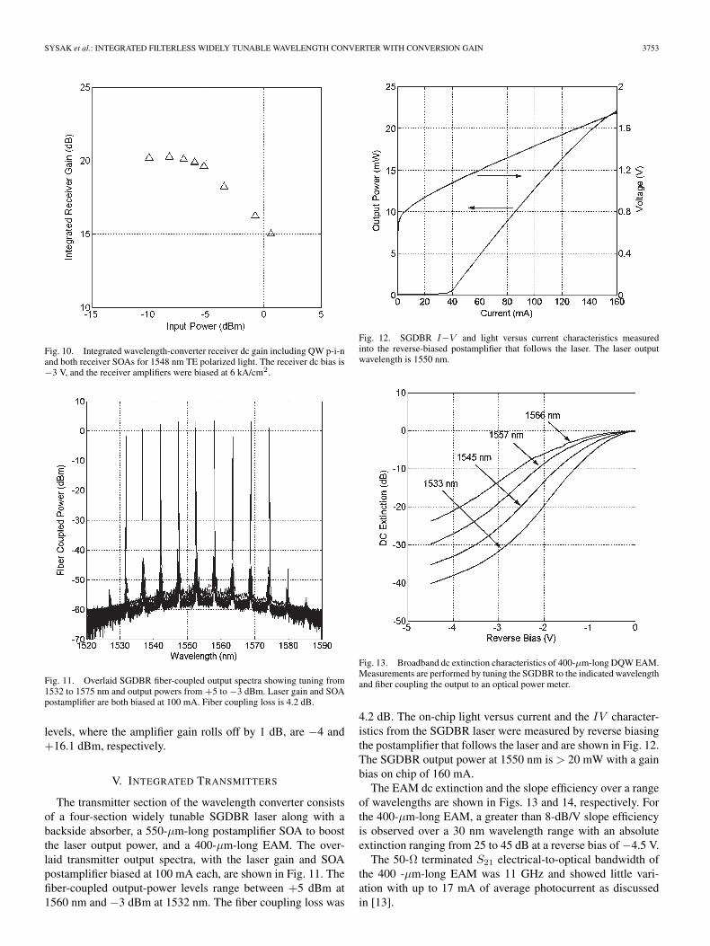
Fig. 10. Integrated wavelength-converter receiver dc gain including QW p-i-nand both receiver SOAs for 1548 nm TE polarized light. The receiver dc bias is−3 V, and the receiver amplifiers were biased at 6 kA/cm2.
Fig. 11. Overlaid SGDBR fiber-coupled output spectra showing tuning from1532 to 1575 nm and output powers from +5 to −3 dBm. Laser gain and SOApostamplifier are both biased at 100 mA. Fiber coupling loss is 4.2 dB.
levels, where the amplifier gain rolls off by 1 dB, are −4 and+16.1 dBm, respectively.
V. INTEGRATED TRANSMITTERS
The transmitter section of the wavelength converter consistsof a four-section widely tunable SGDBR laser along with abackside absorber, a 550-µm-long postamplifier SOA to boostthe laser output power, and a 400-µm-long EAM. The over-laid transmitter output spectra, with the laser gain and SOApostamplifier biased at 100 mA each, are shown in Fig. 11. Thefiber-coupled output-power levels range between +5 dBm at1560 nm and −3 dBm at 1532 nm. The fiber coupling loss was
Fig. 12. SGDBR I−V and light versus current characteristics measuredinto the reverse-biased postamplifier that follows the laser. The laser outputwavelength is 1550 nm.
Fig. 13. Broadband dc extinction characteristics of 400-µm-long DQW EAM.Measurements are performed by tuning the SGDBR to the indicated wavelengthand fiber coupling the output to an optical power meter.
4.2 dB. The on-chip light versus current and the IV character-istics from the SGDBR laser were measured by reverse biasingthe postamplifier that follows the laser and are shown in Fig. 12.The SGDBR output power at 1550 nm is > 20 mW with a gainbias on chip of 160 mA.
The EAM dc extinction and the slope efficiency over a rangeof wavelengths are shown in Figs. 13 and 14, respectively. Forthe 400-µm-long EAM, a greater than 8-dB/V slope efficiencyis observed over a 30 nm wavelength range with an absoluteextinction ranging from 25 to 45 dB at a reverse bias of −4.5 V.
The 50-Ω terminated S21 electrical-to-optical bandwidth ofthe 400 -µm-long EAM was 11 GHz and showed little vari-ation with up to 17 mA of average photocurrent as discussedin [13].

3754 JOURNAL OF LIGHTWAVE TECHNOLOGY, VOL. 25, NO. 12, DECEMBER 2007
Fig. 14. Local slope efficiency dT/dV (in decibels per volt) for the integratedDQW 400-µm-long EAM. Greater than 8 dB/V can be achieved at all outputwavelengths at the appropriate dc-bias position.
Fig. 15. Optical-to-optical S21 bandwidth measurements for the integratedPD-WC with an external 50-Ω termination. The input and output wavelengthsare 1548 and 1555 nm, respectively.
VI. DYNAMIC WAVELENGTH-CONVERTER
MEASUREMENTS
The integrated wavelength converters described in Section IIwere thinned, cleaved into bars, antireflection (AR)-coated,wire-bonded, and mounted on copper studs for testing. Forcharacterization of the PD-WCs, the receiver SOAs are biasedat 6 kA/cm2, and the laser gain and the transmitter postamplifierare biased at 130 and 100 mA, respectively.
The optical-to-optical 3-dB bandwidth of the 50-Ω termi-nated PD-WC was measured using a 20-GHz network analyzerfor a conversion from 1548 to 1555 nm. The results can be seenin Fig. 15 and show a 3-dB bandwidth of approximately 7 GHzwith a reverse bias of −2.5 V. Although not included in the plot,the bandwidth of the PD-WC is relatively insensitive to reverse-
Fig. 16. Average fiber-coupled output power and ER for the integratedPD-WC as a function of the receiver input power. The applied reverse biasis −2.2 V, and the output wavelength is 1555 nm. The eye diagrams are forback-to-back and wavelength-converted signals with −7-dBm receiver inputpower.
bias levels in excess of −1 V. The low-bias dependence is dueto the low doping levels in both the EAM waveguide and theOQWs and to the high doping in the InP n-buffer layer (Fig. 3).Once the applied voltage is sufficient to deplete the EAM andQW p-i-n waveguides, the doping in the buffer (Si at 1 ×1018 cm−3) prevents the depletion width in these componentsfrom increasing as the bias voltage is increased. The fixeddepletion width clamps the depletion capacitance and preservesthe RC time constant that controls the PD-WC bandwidth.
To characterize the switching performance of the PD-WC,the receiver input power, the output wavelength, and the applieddc-bias conditions have been varied, and the wavelength-converted output-signal ER and output power have beenmeasured. The converted ER is measured in the eye diagramwhere the separation between the “one” and “zero” levels is at amaximum. Characterization is performed with a 1548 nm inputsignal at 10 Gb/s using a 231 − 1 psuedorandom bit stream(PRBS). The light from an optical transmitter is fed through anerbium-doped fiber amplifier, an optical filter (0.35 nm), and apolarization controller before it is launched into the deviceusing a lensed fiber. The output PD-WC extinction andoutput-power characteristics are measured by examining thefiber-coupled optical output into a component analyzer.
The effect that increasing the input power to the receiver hason the wavelength-converted extinction and average convertedfiber-coupled output power is shown in Fig. 16. In thisexperiment, the reverse bias is −2.2V. The input wavelength is1548 nm, and the output of the PD-WC is 1555 nm. The eyediagrams are included in the figure for the back-to-back andwavelength-converted signals with an input power of −7 dBm.
As the input power to the receiver increases, both the ERand the output power gradually improve and then level off at12 dB and +0.5 dBm, respectively.
The shape of the ER response is due to a combination ofEAM efficiency effects and receiver saturation effects. For low

SYSAK et al.: INTEGRATED FILTERLESS WIDELY TUNABLE WAVELENGTH CONVERTER WITH CONVERSION GAIN 3755
input powers where the receiver SOAs can operate in theirlinear regime, the increases in the input power create corre-sponding increases in the photocurrent from the QW p-i-n and,hence, an increasing voltage over the load resistor. This increasein voltage generates larger swings in EAM transmission andresults in larger PD-WC ERs.
However, as the input power to the receiver continues toincrease, several factors begin to limit device performance. Asvoltage swings from the receiver get larger, the integrated EAMis driven well beyond the optimal slope efficiency point inFig. 14. Under these conditions, even though the preamplifiedreceiver is continuing to generate larger photocurrent levels, thereduced EAM efficiency leads to smaller incremental increasesin the PD-WC extinction.
The other factor that plays an important role in thewavelength-converter extinction is the receiver preamplifierresponse (Fig. 10). As the input powers approach the amplifiersaturation power, the optical gain from the receiver is degraded.Under these conditions, the shape of the amplified signal tothe photodetector becomes distorted by the gain overshoot, andthe photocurrent that is used to drive the integrated EAM addssignificant noise to the converted signals, distorting the ERfrom the PD-WC.
The average output-power characteristics from the wave-length converter, which are shown in Fig. 16, are controlledby a combination of the EAM “OFF” state and slope efficiency.For low input powers, the output power from the PD-WCinitially increases before finally rolling over due to the EAMslope-efficiency degradation and amplifier saturation. Since theextinction and the output power for the fixed-bias conditionsused in Fig. 16 do not significantly improve beyond an inputpower of −7 dBm, further device characterization is performedat this input power.
In the next set of experiments, the wavelength-converteroutput-power and ER performance is characterized over arange of electrical bias voltages and over a range of outputwavelengths using the −7 dBm input power. The results areshown in Figs. 17 and 18 for the wavelength-converted ERsand the average output powers, respectively. Over the outputwavelengths ranging from 1533 to 1564 nm, greater than10-dB extinction is achievable by setting the appropriatereverse-bias conditions. For a particular output wavelength,as the reverse bias is moved toward the bias conditions thatcorrespond with the maximum EAM slope efficiency (Fig. 14),the output extinction is improved. However, as the bias isincreased and the output extinction improves, the output powerfrom the wavelength converter is reduced. For the 10-dBextinction at output wavelengths of 1533, 1545, 1555, and1564 nm, the corresponding reverse biases required are −1.35,−1.6, −1. 9, and −2.4V, and the output powers at these biasesare −5.2, −2.6, −1, and −0.5 dBm, respectively.
VII. DIGITAL-SYSTEM EXPERIMENTS
To examine the performance of the integrated wavelengthconverter in a digital transmission system, a set of bit-error-rate (BER) measurements was performed using the test setupshown in Fig. 19. In the first set of measurements, the input
Fig. 17. Average fiber-coupled output power versus wavelength and reversebias. The 10-dB ER bias points are −1.3, −1.7, −2.2, and −2.3 V for 1533,1545, 1557, and 1565 nm, respectively. The input wavelength is 1548 nm, andthe input power is −7 dBm.
Fig. 18. Wavelength-converted ER from the PD-WC. The bias points for the10-dB ER are −1.2, −1.6, −1.9, and −2.4 V at output wavelengths of 1533,1545, 1557, and 1566 nm, respectively. The input wavelength is 1548 nm, andthe input power is −7 dBm.
power to the PD-WC receiver is identified, which minimizesthe system power penalty for a conversion between 1548 and1563 nm. This input power is then used to perform wavelengthswitching between a single input wavelength and a range ofoutput wavelengths, followed by switching from a range of in-put wavelengths to a single output wavelength. The BER mea-surements were performed using a 231 − 1 PRBS at 10 Gb/swith nonreturn-to-zero data. The SGDBR bias conditions andreceiver-amplifier bias conditions are the same, as outlined inSection VI.
The first set of BER measurements is used to identify theinput power to the PD-WC that will give the minimum powerpenalty for wavelength switching between 1548 and 1563 nm.

3756 JOURNAL OF LIGHTWAVE TECHNOLOGY, VOL. 25, NO. 12, DECEMBER 2007
Fig. 19. Test setup used for digital-system experiments. For experimentswhere a nonfixed wavelength input source is used, the transmitter light source(λin) is replaced with a tunable laser.
Fig. 20. Wavelength-converted and back-to-back BER measurements for var-ious input powers at a reverse bias of −3.1 V. The input and output wavelengthsare 1548 and 1563 nm, respectively.
In these experiments, a fixed reverse bias is applied to the EAMand QW p-i-n for the maximum EAM efficiency (−2.8V). Theresults for these BER experiments are shown in Fig. 20 forinput-power levels of −7.5, −10.5, −11.2, and −12.8 dBm.The power penalty for each PD-WC input power is calculatedas the difference in optical power into the external receiverthat is required for a BER of 10−9 between the wavelength-converted signals and the signals from the transmitter in the testsetup (back to back). As the power to the receiver increasesfrom −12.8 to −11.2 dBm, the BER results show that thepower penalty decreases. However, as the receiver power isincreased from −11.2 to −10.5 dBm, then to −7.5 dBm, thepower penalty actually increases despite an increase in thewavelength-converted signal ER. The increase in the powerpenalty with higher input powers is accompanied by a changein the BER slope. The change in the slope of the BER curvesat higher input powers indicates a redistribution of the noisestatistics through the device and most likely comes as a result ofthe saturation effects in the receiver preamplifier. This behavioris not necessarily unexpected as other authors have seen similarnoise redistribution for preamplified receivers operating belowtheir 1-dB gain-compression points [20]. The power penalty asa function of the input power and the wavelength-converted
Fig. 21. Summary of wavelength-converted ER and BER power penalty alongwith eye diagrams from BER experiments using various receiver input powers.The input and converted wavelengths are 1548 and 1563 nm, respectively, withan applied bias of −2.8V.
Fig. 22. BER measurement results for the PD-WC with an input power of−11 dBm and various output wavelengths. Bias conditions are adjusted toachieve 8–9-dB ER. The input wavelength is 1548 nm.
signal ER for output signals from the PD-WC are shown inFig. 21. The figure also contains the wavelength-converted eyediagrams corresponding to each input-power level. In the eyediagrams, the additive noise on the “one” level at the higherinput powers is a result of the receiver SOA gain overshoot andmost likely contributes to the noise redistribution seen in theBER results in Fig. 20.
Using the optimized input-power level (−11.2 dBm), thewavelength-conversion BER experiments were performed us-ing an input signal at 1548 nm and an output wavelengthranging from 1531 to 1564 nm. The results are shown in Fig. 22.The reverse-bias points at output wavelengths of 1563, 1553,1542, and 1531 nm were −2.9, −2.7, −2.0, and −1.5 V, re-spectively, and were selected to achieve wavelength-convertedERs between 8 and 9 dB. A summary of the output extinctionand output power of the device at each of these bias conditions

SYSAK et al.: INTEGRATED FILTERLESS WIDELY TUNABLE WAVELENGTH CONVERTER WITH CONVERSION GAIN 3757
Fig. 23. Output extinction and average output facet power (fiber coupling lossremoved) in BER measurements to achieve less than 1-dB power penalty forwavelength-converted signals.
Fig. 24. BER measurement results for fixed out wavelength (1553 nm) andvariable input wavelengths. The receiver power is −11 dBm for all inputwavelengths, and the PD-WC reverse bias is set to achieve the maximum EAMslope efficiency.
(with the 4.2-dB fiber coupling loss removed) is shown inFig. 23. Taking into account the input facet power of −11 dBm,this gives gains of the wavelength converter of 9, 11, 12, and13 dBm at output wavelengths of 1531, 1542, 1553, and1563 nm, respectively.
The remaining critical factor for broadband operation ofthe integrated PD-WC is the performance of the device undervarious input-wavelength conditions. A set of BER experimentswas performed, where the input wavelength was varied between1535 and 1560 nm and where the output wavelength was heldfixed at 1553 nm. The results are shown in Fig. 24, along withthe back-to-back measurements at 1530 and 1550 nm. Less than2.5-dB power penalty is observed when the bias conditions onthe PD-WC were set for the optimal extinction characteristics.The input power in each of these experiments was held fixed
at −11 dBm. The ERs for output wavelengths of 1535, 1550,and 1560 nm, were 7.4, 9, and 6.5 dB, respectively. The lowerERs at input wavelengths of 1530 and 1560 nm are a result ofthe increase in optical loss at the low end of the wavelengthspectrum shown in Fig. 5 and the decrease in optical gain asthe operating wavelength moves away from the PL peak of theOQW stack.
VIII. CONCLUSION
We have presented a detailed study of a monolithic 10-Gb/sPD-WC that consists of a widely tunable laser source andoptical receiver. The device is fabricated on a DQW integrationplatform and utilizes QWs for modulation efficiency in the in-tegrated EAMs without incorporating multiple regrowth steps.The dynamic measurements of the wavelength-converted ERsshow in excess of 10 dB over the full wavelength tuning range.Digital-system-performance measurements with a fixed wave-length input signal show less than 1 dB power penalty for theconverted signals over output wavelengths between 1533 and1564 nm with a facet-to-facet conversion gain between 9 and13 dB. The BER measurements with variable input wavelengthsand a fixed output wavelength show less than 2.5-dB powerpenalty for input wavelengths between 1535 and 1560 nm.
ACKNOWLEDGMENT
The authors would like to thank JDS Uniphase Corporationfor the AR coatings, along with Prof. J. Bowers of the Univer-sity of California—Santa Barbara and M. J. Paniccia of IntelCorporation for their support during this work.
REFERENCES
[1] S. B. Yoo, “Wavelength conversion technologies for WDM network ap-plications,” J. Lightw. Technol., vol. 14, no. 6, pp. 955–966, Jun. 1996.
[2] W. Idler, K. Daube, G. Laube, M. Schilling, P. Wiedemann, K. Dutting,M. Klenk, E. Lach, and K. Wunstel, “10 Gb/s wavelength conversionwith integrated multiquantum-well-based 3-port Mach–Zehnder interfer-ometer,” IEEE Photon. Technol. Lett., vol. 16, no. 9, pp. 1163–1165,Sep. 1998.
[3] S. Hojfeldt, S. Bischoff, and J. Mork, “All-optical wavelength conversionand signal regeneration using an electroabsorption modulator,” J. Lightw.Technol., vol. 18, no. 8, pp. 1121–1127, Aug. 2000.
[4] S. Kodama, T. Yoshimatsu, and H. Ito, “500 Gb/s optical gate monolith-ically integrated photodiode and electroabsorption modulator,” Electron.Lett., vol. 40, no. 9, pp. 555–556, Apr. 2004.
[5] A. Kelley, D. Marcenac, and D. Nesset, “40 Gb/s wavelength conversionover 24.6 nm using FWM in a semiconductor optical amplifier with anoptimized MQW active region,” Electron. Lett.,, vol. 33, no. 25, pp. 2123–2124, Dec. 1997.
[6] V. Lal, M. L. Masanovic, J. A. Summers, L. A. Coldren, andD. J. Blumenthal, “Performance optimization of an InP-based widely tun-able all-optical wavelength converter operating at 40 Gb/s,” IEEE Photon.Technol. Lett., vol. 18, no. 4, pp. 577–579, Feb. 2006.
[7] J. Leuthold, P. Besse, E. Gamper, M. Dulk, S. Fisher, G. Geukos,and H. Melchior, “All-optical Mach–Zehnder interferometer wavelengthconverters and switches with integrated data and control signal sep-aration scheme,” J. Lightw. Technol., vol. 17, no. 6, pp. 1056–1066,Jun. 1999.
[8] R. Doshi, M. L. Masanovic, and D. J. Blumenthal, “Demonstration of anyλin to any λout wavelength conversion using a 2-stage all-optical wave-length converter consisting of a XGM SOA-WC and InP monolithically-integrated widely-tunable MZI SOA-WC,” in Proc. Meeting LEOS, 2003,vol. 2, pp. 477–478.

3758 JOURNAL OF LIGHTWAVE TECHNOLOGY, VOL. 25, NO. 12, DECEMBER 2007
[9] J. S. Barton, E. J. Skogen, M. L. Masanovic, J. Raring, M. N. Sysak,L. Johansson, S. P. DenBaars, and L. A. Coldren, “Photonic integrated cir-cuits based on sampled-grating distributed-Bragg-reflector lasers,” Proc.SPIE-Int. Soc. Opt. Eng., vol. 4998, pp. 43–54, 2003.
[10] M. N. Sysak, J. W. Raring, J. S. Barton, H. N. Poulsen, D. J. Blumenthal,and L. A. Coldren, “Extinction ratio regeneration, signal re-amplification(2R), and broadband wavelength switching using a monolithically inte-grated photocurrent driven wavelength converter,” Opt. Express, vol. 14,no. 23, pp. 11343–11348, Nov. 2006.
[11] M. N. Sysak, L. A. Johannson, J. W. Raring, H. N. Poulsen,D. J. Blumenthal, and L. A. Coldren, “Broadband return to zero (RZ)signal regeneration and broadband wavelength conversion using a mono-lithically integrated, photocurrent driven wavelength converter,” Electron.Lett., vol. 42, no. 25, pp. 1479–1481, Dec. 2006.
[12] Y. A. Akulova, G. A. Fish, H. Xu, E. Hall, M. C. Larson, P. Abraham,H. Marchand, C. Turner, C. Coldren, E. Hegblom, T. A. Strand, andL. A. Coldren, “Monolithically integrated tunable transmitters,” presentedat the Integrated Photonics Research and Applications (IPRA), San Diego,CA, Apr. 11–15, 2005, Paper IWF4.
[13] M. N. Sysak, J. W. Raring, J. S. Barton, M. Dummer,D. J. Blumenthal, and L. A. Coldren, “A single regrowth integrationplatform for photonic circuits incorporating tunable SGDBR laser andquantum well EAMs,” IEEE Photon. Technol. Lett., vol. 18, no. 15,pp. 1630–1632, Aug. 2006.
[14] M. N. Sysak, J. W. Raring, D. J. Blumenthal, and L. A. Coldren, “Aquantum well EAM-SGDBR widely tunable transmitter fabricated in anovel dual quantum well integration platform,” in Proc. DRC, IIA-2,Jun. 2006, pp. 15–16.
[15] J. Dow and D. Redfield, “Toward a unified theory of Urbach’s rule andexponential absorption edge,” Phys. Rev. B, Condens. Matter, vol. 5, no. 2,pp. 594–609, Jan. 1972.
[16] J. W. Raring, E. J. Skogen, C. S. Wang, J. S. Barton, G. B. Morrison,S. Demiguel, S. P. Denbaars, and L. A. Coldren, “Design and demonstra-tion of novel QW intermixing scheme for the integration of UTC-typephotodiodes with QW-based components,” IEEE J. Quantum Electron.,vol. 42, no. 2, pp. 171–181, Feb. 2006.
[17] V. Lal, W. Donat, A. Tauke-Pedretti, L. A. Coldren, andD. J. Blumenthal, “Broadband rate-equation model including many-body gain for WDM traveling-wave SOAs,” in Proc. NUSOD, Berlin,Germany, 2005, pp. 125–126.
[18] A. Tauke-Pedretti, M. Dummer, J. S. Barton, M. N. Sysak, J. W. Raring,and L. A. Coldren, “High saturation power and high gain integratedreceivers,” IEEE Photon. Technol. Lett., vol. 17, no. 10, pp. 2167–2169,Oct. 2005.
[19] S. Hojfeldt and J. Mork, “Modeling of carrier dynamics in quantum-wellelectroabsorption modulators,” IEEE J. Sel. Topics Quantum Electron.,vol. 8, no. 6, pp. 1265–1276, Dec. 2002.
[20] K. Morito, M. Ekawa, T. Watanabe, and Y. Kotaki, “High-output-powerpolarization-insensitive semiconductor optical amplifier,” J. Lightw.Technol., vol. 21, no. 1, pp. 176–181, Jan. 2001.
Matthew N. Sysak (M’01) was born inSmithtown, NY, in 1976. He received the B.S.degree in chemical engineering from PennsylvaniaState University, University Park, in 1998 and theM.S and Ph.D. degrees in electrical and computerengineering from the University of California—Santa Barbara, in 2002 and 2005, respectively. Hisdissertation focused on the design and fabrication ofmonolithically integrated widely tunable sampled-grating distributed-Bragg-reflector semiconductorlasers, semiconductor optical amplifiers, electroab-
sorption modulators, and photodetectors for wavelength conversion and signalregeneration using a novel dual quantum-well integration platform.
He is currently working as a Postdoctoral Researcher with Prof. J. Bowersin the Ultrafast Optoelectronics Group, Department of Electrical and ComputerEngineering, University of California—Santa Barbara, focusing on the designand fabrication of ultralinear monolithically integrated photonic links.
Dr. Sysak is a member of the Optical Society of America and The Interna-tional Society for Optical Engineers.
James W. Raring (M’01) received the B.S. de-gree from California Polytechnic State University,San Luis Obispo, in 2001 and the Ph.D. de-gree in materials science from the University ofCalifornia, Santa Barbara, in 2006. His Ph.D. re-search focused on the design, growth, and fabricationof high-functionality wavelength-agile InGaAsP-based photonic integrated circuits (PICs). By cou-pling quantum well intermixing with MOCVDregrowth, he combined widely tunable sampled grat-ing DBR lasers, 40-Gb/s electroabsorption modula-
tors, low-confinement high-saturation power semiconductor optical amplifiers,and 40-Gb/s unitraveling carrier photodiodes to demonstrate the first single-chip 40-Gb/s optical transceiver.
In 2006, he joined the RF/Optoelectronic Group, Sandia National Laborato-ries, Albuquerque, NM, where he is currently working on leading edge PICs.He is the author or coauthor of more than 75 technical papers.
Dr. Raring is a member of the IEEE Lasers and Electro-Optics Society,the Optical Society of America, and the International Society for OpticalEngineers.
Jonathon S. Barton (S’97–M’98) received the B.S.degree in electrical engineering and material sciencefrom the University of California—Davis in 1997and the Ph.D. degree in electronic materials from theUniversity of California—Santa Barbara.
He was an Intel Fellow during the time he receivedhis doctorate. Currently, he is an Assistant ProjectScientist for the Laser Switched Optical Router De-fense Advanced Research Projects Agency grant,working on the growth, fabrication, and high-speedtesting of many monolithic optoelectronic compo-
nents such as tunable lasers, modulators, and photocurrent-driven wavelengthconverters. He is also currently with the Department of Materials, University ofCalifornia—Santa Barbara.
Dr. Barton is a member of the IEEE Lasers and Electro-Optics Society,the Optical Society of America, and The International Society for OpticalEngineers.
Henrik N. Poulsen received the M.Sc.E.E. degreefrom the Technical University of Denmark, Lyngby,Denmark, in 1995.
From 1995 to 2001, he first worked as a ResearchAssociate and later as an Associate Research Pro-fessor in the field of high-speed wavelength-divisionmultiplexing and optical time-division multiplexing.In 2001, he moved from Copenhagen, Denmark, toSanta Barbara, CA, to join Calient Networks, wherehe worked on optical amplification and performancemonitoring for all-optical microelectromechanical-
system-based switches. He is currently working as an Associate ProjectScientist with Prof. D. J. Blumenthal in the Optical Communications andPhotonics Network Group, Department of Electrical and Computer Engi-neering, University of California—Santa Barbara. His main research area isall-optical packet switching using all-optical interferometric structures. Hismain interests were ultrahigh-speed optical signal processing using nonlinearfiber and semiconductor materials, mainly semiconductor optical amplifiers,interferometric structures, and electroabsorption modulators.

SYSAK et al.: INTEGRATED FILTERLESS WIDELY TUNABLE WAVELENGTH CONVERTER WITH CONVERSION GAIN 3759
Daniel J. Blumenthal (S’91–M’93–SM’97–F’03)received the B.S.E.E. degree from the Universityof Rochester, Rochester, NY, in 1981, the M.S.E.E.degree from Columbia University, New York, NY, in1988, and the Ph.D. degree from the University ofColorado at Boulder, Boulder, in 1993.
In 1981, he was with the StorageTek, Louisville,CO, in the area of optical data storage. In 1986,he was with Columbia University in the areas ofphotonic switching systems, ultrafast all-optical net-works, and signal processing. From 1993 to 1997,
he was an Assistant Professor with the School of Electrical and ComputerEngineering, Georgia Institute of Technology, Atlanta. He is currently a Pro-fessor with the Department of Electrical and Computer Engineering, Univer-sity of California—Santa Barbara, and the Associate Director for the Centeron Multidisciplinary Optical Switching Technology. He heads the OpticalCommunications and Photonic Networks Research. He is the Cofounder ofCalient Networks, a manufacturer of photonic switching systems, which isbased in San Jose, CA. His current research areas are in optical communi-cations, wavelength-division multiplexing, photonic packet-switched and all-optical networks, all-optical wavelength conversion, and optical subcarriermultiplexing. He has authored or coauthored over 100 papers in these andrelated areas.
Dr. Blumenthal is a member of the Optical Society of America. He isthe recipient of the 1999 Presidential Early Career Award for Scientists andEngineers, the 1994 National Science Foundation Young Investigator Award,and the 1997 Office of Naval Research Young Investigator Program Award.He served as an Associate Editor for the IEEE PHOTONICS TECHNOLOGY
LETTERS and the IEEE TRANSACTIONS ON COMMUNICATIONS. He was aGuest Editor for the IEEE JOURNAL OF LIGHTWAVE TECHNOLOGY SpecialIssue in Photonic Packet Switching Systems, Technologies, and Techniques,which was published in December 1998. He also served as the Program Chairand the Technical Program Committee member on numerous conferences.
Larry A. Coldren (S’67–M’72–SM’77–F’82) re-ceived the Ph.D. degree in electrical engineeringfrom Stanford University, Stanford, CA, in 1972.
He is the Fred Kavli Professor of optoelectronicsand sensors with the University of California—SantaBarbara (UCSB). He is also the Chairman and ChiefTechnology Officer of Agility Communications, Inc.After 13 years in the research area at Bell Labora-tories, Murray Hill, NJ, he has been with the UCSBsince 1984, where he now holds appointments in theDepartments of Materials and Electrical and Com-
puter Engineering and is the Director of the Optoelectronics Technology Center.In 1990, he cofounded Optical Concepts, later acquired as Gore Photonics,to develop novel vertical-cavity surface-emitting laser (VCSEL) technology,and in 1998, he cofounded Agility Communications, Inc. to develop widelytunable integrated transmitters. At Bell Labs, he initially worked on waveguidedsurface-acoustic-wave signal-processing devices and coupled-resonator filters.He later developed tunable coupled-cavity lasers using novel reactive-ion-etching technology that he created for the then new InP-based materials. At theUCSB, he continued working on multiple-section tunable lasers; in 1988, heinvented the widely tunable multielement mirror concept, which is now funda-mental to many of Agility’s products. During the late 1980s, he also developedefficient vertical-cavity multiple-quantum-well modulators, which led to thenovel VCSEL designs that provided unparalleled levels of performance. Hecontinues to be active in developing new photonic integrated circuit (PIC) andVCSEL technology, including the underlying materials growth and fabricationtechniques. In recent years, for example, he has been involved in the creationof vertical and in-plane GaN-based emitters, efficient all-epitaxial InP-basedVCSELs, and a variety of PICs incorporating numerous optical elements forwidely tunable integrated transmitters, receivers, and wavelength converters.He has authored or coauthored over 700 papers, five book chapters, and onetextbook and is the holder of 36 patents.
Dr. Coldren is a fellow of the Optical Society of America and the Institutionof Electrical Engineers and a member of the National Academy of Engineering.He is the recipient of the 2004 John Tyndall Award. He has presented dozens ofinvited and plenary talks at major conferences.