Monolithically Integrable RF MEMS...
7
JOURNAL OF SEMICONDUCTOR TECHNOLOGY AND SCIENCE, VOL.2, NO. 1, MARCH, 2002 49 Monolithically Integrable RF MEMS Passives Eun-Chul Park, Yun-Seok Choi, Jun-Bo Yoon, and Euisik Yoon Abstract − This paper presents high performance MEMS passives using fully CMOS compatible, monolithically integrable 3-D RF MEMS processes for RF and microwave applications. The 3-D RF MEMS technology has been developed and investigated as a viable technological option, which can break the limit of the conventional IC technology. We have demonstrated the versatility of the technology by fabricating various 3-D thick-metal microstructures for RF and microwave applications, such as spiral/solenoid inductors, transformers, and transmission lines, with a vertical dimension of up to 100 µm. To the best of our knowledge, we report that we are the first to construct a fully integrated VCO with MEMS inductors, which has achieved a low phase noise of –124 dBc/Hz at 300 kHz offset from a center frequency of 1 GHz. Index Terms − RF MEMS, surface micromachining, inductor, transformer, transmission line, VCO. I. INTRODUCTION Modern RF communication systems require stringent specifications for RF components. Despite much work, which has been done on the integration of RF systems into a single chip, many components remain off-chip. This is because the RF passives with the required performance are not available in the standard silicon process. Many recent studies have shown that two aspects are extremely important in order to obtain high- performance integrated passive components when the signal frequency is in the GHz range. One is the metal thickness and the other is how far the device is isolated from the lossy substrate. For these two reasons, research has been performed to investigate other technological options among available fabrication processes. With this in mind, various micromachining technologies, which have been developed for implementing microelectromechanical systems (MEMS), have been investigated and applied to RF and microwave applications [1-3]. In this paper, we provide a surface micromachining technique aimed at the monolithic integration of free 3-D microstructures, which are beneficial to RF and microwave applications. We also present the performances of inductors, transformers, and transmission lines, which have been fabricated using the 3-D MEMS process. Finally, we demonstrate fully integrated voltage controlled oscillators (VCOs) which have been fabricated using a conventional 0.18 µm CMOS process for the actives and integrating high-Q inductors on top of the circuit as a post IC process utilizing the 3-D MEMS process developed in this work. II. FABRICATION TECHNIQUE A. Fabrication Process The fabrication process is very simple: first, make a 3- D photoresist mold having arbitrarily-shaped upper recess regions; second, fill both the lower and upper recess regions with metal; and finally remove the photoresist molds. The process flow is shown in Fig. 1, starting with a Manuscript received January 12, 2002; revised March 7, 2002. Department of Electrical Engineering and Computer Science (Division of Electrical Engineering) Korea Advanced Institute of Science and Technology 373-1, Guseong-dong, Yuseong-gu, Daejeon, 305-701, Republic of Korea (e-mail : [email protected]) Tel : +82-42 869 5462 Fax : +82 42 869 8530
Transcript of Monolithically Integrable RF MEMS...
JOURNAL OF SEMICONDUCTOR TECHNOLOGY AND SCIENCE, VOL.2, NO. 1, MARCH, 2002
49
Monolithically Integrable RF MEMS Passives
Eun-Chul Park, Yun-Seok Choi, Jun-Bo Yoon, and Euisik Yoon
Abstract− This paper presents high performance MEMS passives using fully CMOS compatible, monolithically integrable 3-D RF MEMS processes for RF and microwave applications. The 3-D RF MEMS technology has been developed and investigated as a viable technological option, which can break the limit of the conventional IC technology. We have demonstrated the versatility of the technology by fabricating various 3-D thick-metal microstructures for RF and microwave applications, such as spiral/solenoid inductors, transformers, and transmission lines, with a vertical dimension of up to 100 µm. To the best of our knowledge, we report that we are the first to construct a fully integrated VCO with MEMS inductors, which has achieved a low phase noise of –124 dBc/Hz at 300 kHz offset from a center frequency of 1 GHz. Index Terms − RF MEMS, surface micromachining, inductor, transformer, transmission line, VCO.
I. INTRODUCTION
Modern RF communication systems require stringent specifications for RF components. Despite much work, which has been done on the integration of RF systems into a single chip, many components remain off-chip.
This is because the RF passives with the required performance are not available in the standard silicon process. Many recent studies have shown that two aspects are extremely important in order to obtain high-performance integrated passive components when the signal frequency is in the GHz range. One is the metal thickness and the other is how far the device is isolated from the lossy substrate. For these two reasons, research has been performed to investigate other technological options among available fabrication processes.
With this in mind, various micromachining technologies, which have been developed for implementing microelectromechanical systems (MEMS), have been investigated and applied to RF and microwave applications [1-3]. In this paper, we provide a surface micromachining technique aimed at the monolithic integration of free 3-D microstructures, which are beneficial to RF and microwave applications. We also present the performances of inductors, transformers, and transmission lines, which have been fabricated using the 3-D MEMS process. Finally, we demonstrate fully integrated voltage controlled oscillators (VCOs) which have been fabricated using a conventional 0.18 µm CMOS process for the actives and integrating high-Q inductors on top of the circuit as a post IC process utilizing the 3-D MEMS process developed in this work.
II. FABRICATION TECHNIQUE
A. Fabrication Process
The fabrication process is very simple: first, make a 3-D photoresist mold having arbitrarily-shaped upper recess regions; second, fill both the lower and upper recess regions with metal; and finally remove the photoresist molds.
The process flow is shown in Fig. 1, starting with a
Manuscript received January 12, 2002; revised March 7, 2002. Department of Electrical Engineering and Computer Science
(Division of Electrical Engineering) Korea Advanced Institute of Science and Technology 373-1, Guseong-dong, Yuseong-gu, Daejeon, 305-701, Republic of Korea (e-mail : [email protected]) Tel : +82-42 869 5462 Fax : +82 42 869 8530
E. C. PARK et al. : MONOLITHICALLY INTEGRABLE RF MEMS PASSIVES 50
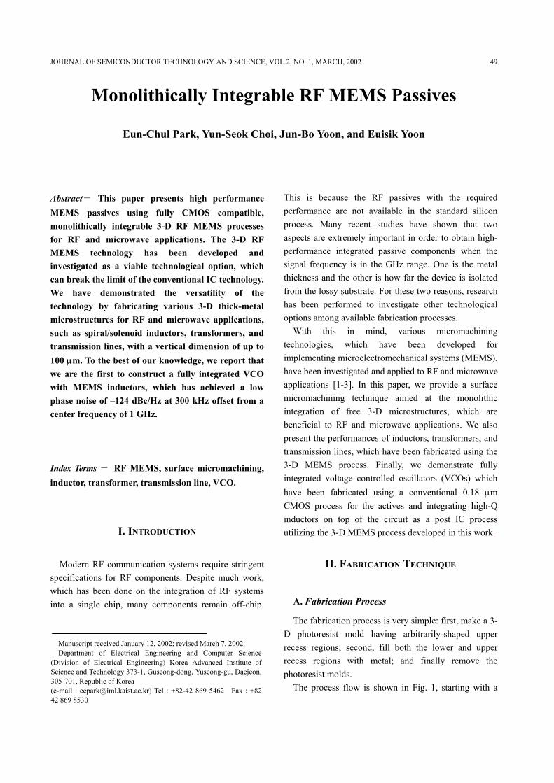
substrate on which the bottom seed metal (Ti/Cu) is deposited. The bottom Cu electrode is then formed using conventional lithography with a thick photoresist followed by electroplating. After removing the photoresist, another thick photoresist (usually over 50 µm in thickness) is spun onto the wafer, as shown in Fig. 1.(a). A two-step UV exposure follows with two different photomasks and exposure times. A single step development reveals the 3-D photoresist mold as shown in Fig. 1.(b). The typical MESD process conditions can be found in [4]. Once the 3-D photoresist mold is fabricated, the lower recess region is filled with the electroplated metal to form the posts in Fig. 1.(c). The Cu electroplating solution used in this work is defined in [4]. Since the post’s electroplating is done filling upward from the bottom of the lower recess region, we can obtain fully-filled, robust posts. After the post electroplating, the surface is covered with another
seed metal (Cu) as shown in Fig. 1.(d). To make sure that the next electroplating occurs only in the upper recess regions, as shown in Fig. 1.(f), the topmost seed metal is removed as shown in Fig. 1.(e). The dashed line shown in Fig. 1.(d) indicates the boundary to which the mechanical polishing is done. Next, another electroplating is performed to fill the upper recess regions with metal as shown in Fig. 1.(f). Since all the second seed metal in the upper recess regions are electrically connected to the bottom seed metal through the metal posts, all the upper recess regions are simultaneously filled during the electroplating process. This makes it possible to obtain longer and arbitrarily shaped, suspended structures. Finally, the sacrificial 3-D photoresist mold is removed with acetone and the bottom seed metal is etched for electrical isolation between devices. The final suspended microstructure is shown in Fig. 1.(g).
Substrate
Shallow exposure
Deep exposure
Thick photoresist ( > 50µm)
Bottom Cu
Fig.1.(a) Double exposure
Fig.1.(b) Single development
Seed metal (Ti/Cu)
Fig.1.(c) Post plating
Fig.1.(d) Seed (Cu) deposition
Fig.1.(e) Surface polishing
Fig.1.(f) Top plating
Top Cu
Fig.1.(g) Finishing
Post Cu
Seed metal (Cu)
Fig. 1. Proposed fabrication process flow
(a) Double exposure
(b) Single development
(c) Post plating
(d) Seed(Cu) deposition
(e) Surface polishing
(f) Stop plating
(g) Finishing
JOURNAL OF SEMICONDUCTOR TECHNOLOGY AND SCIENCE, VOL.2, NO. 1, MARCH, 2002
51
B. Fab
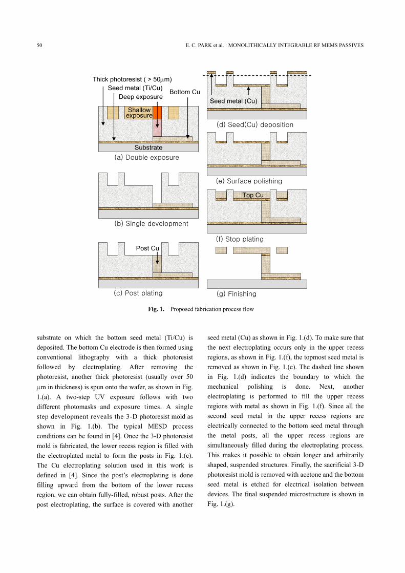
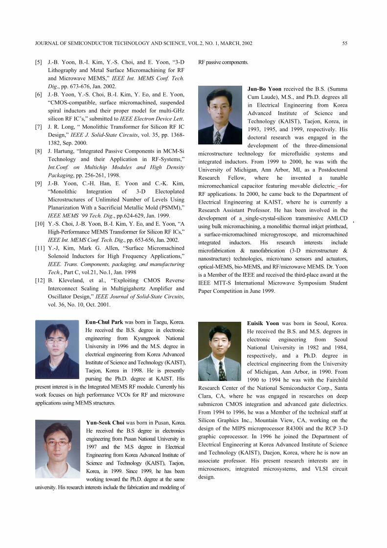
Fig. 2 showinductor, solentransmission ltechnology. Frothat they have bare suspended capability of thsuspended linesresiding in the we have demonµm over the suband a coplanar substrate. All been made usin1 and describetechnology is vfairly- complica
III. H
As the operat
100µm
Fig.2.(b)
Fig.2.(d)Fig.2.(c)
Fig.2.(a)
100µm
Fig.2.(b)
Fig.2.(d)Fig.2.(c)
Fig.2.(a)
Fig. 2. SEM view of fabricated 3-D passives
(a)
(c) (d)
(b)
ricated RF MEMS Passives
s the SEM photographs of the spiral oid inductor, 1:1 transformer and
ine fabricated using the proposed m the structures in Fig. 2, one can see een easily shaped in many variations and flat, due to the excellent planarization e sacrificial photoresist mold. The flat also indicate no internal stress gradient electroplated metal structures. In Fig. 2, strated a spiral inductor suspended 100 strate, a solenoid inductor, a transformer, waveguide suspended 50 µm over the
these multi-level microstructures have g the fundamental process shown in Fig. d above. This demonstrates that our ersatile enough to construct multi-level, ted microstructures.
IGH-Q MEMS INDUCTORS
ing frequency of recent silicon RF IC’s
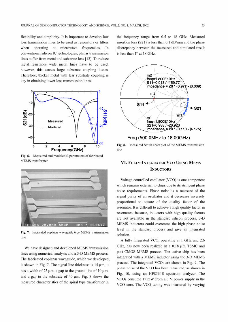
move into the multi-GHz frequency range, it becomes difficult to achieve affordable Q-factors (>15) from on-chip inductors fabricated using conventional thin-film, planar IC processes. Recently, we have reported a new MEMS fabrication process developed for RF and microwave applications [5]. This process allows us to fabricate arbitrary shaped, highly suspended metal microstructures, which are fully CMOS-compatible, can be manufactured in a stable process and exhibit structural robustness. In this chapter, we report on the RF performance of the suspended spiral inductors fabricated using our new fabrication technology based on the standard silicon substrate (1~30Ω⋅cm).
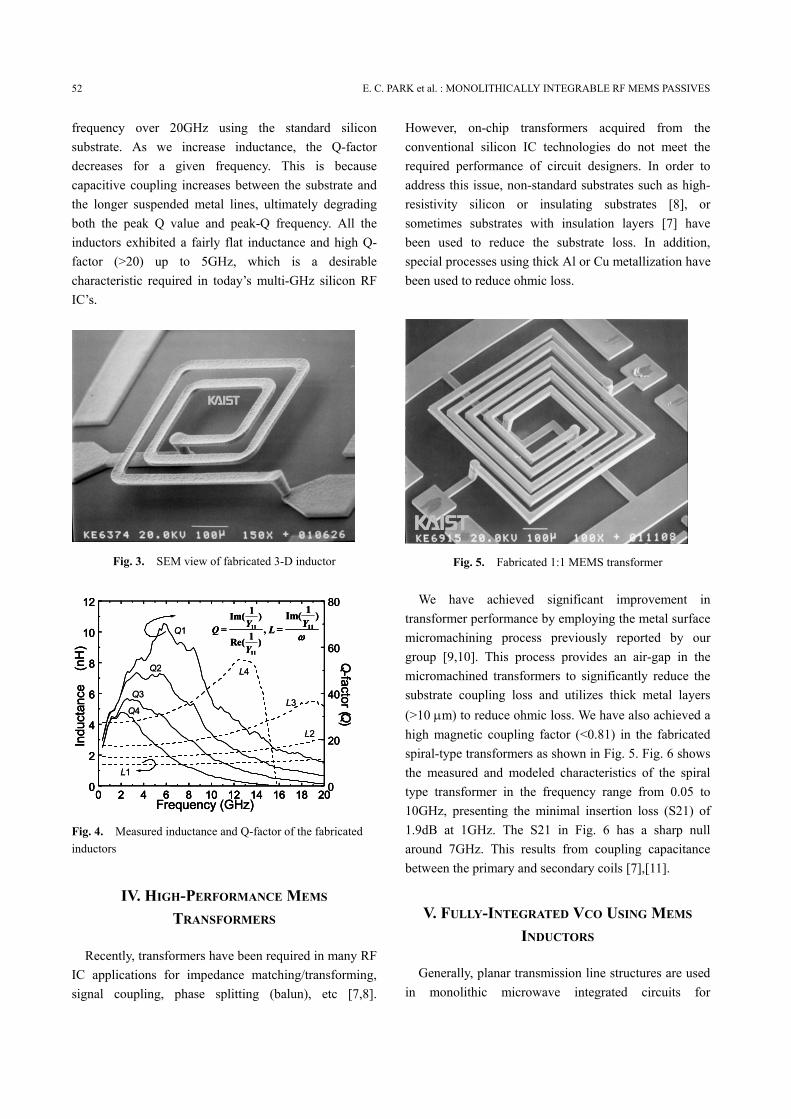
Fig. 3 shows the SEM microphotograph of the fabricated inductor, which clearly reveals the flat and smooth surface of the suspended inductor together with robust post structures [6]. We measured the on-wafer RF from 0.2 GHz to 20 GHz using an HP 8510C network analyzer. Fig. 4 shows the characteristics of the fabricated inductors along with the definition of inductance (L) and Q-factor (Q) used in this work. We have achieved a peak Q-factor of 70 at 6 GHz, an inductance of 1.38 nH (at 1 GHz) and a self-resonant
E. C. PARK et al. : MONOLITHICALLY INTEGRABLE RF MEMS PASSIVES 52
frequency over 20GHz using the standard silicon substrate. As we increase inductance, the Q-factor decreases for a given frequency. This is because capacitive coupling increases between the substrate and the longer suspended metal lines, ultimately degrading both the peak Q value and peak-Q frequency. All the inductors exhibited a fairly flat inductance and high Q-factor (>20) up to 5GHz, which is a desirable characteristic required in today’s multi-GHz silicon RF IC’s.
Fig. 3. SEM view of fabricated 3-D inductor
0 2 4 6 8 10 12 14 16 18 200
2
4
6
8
10
12
Frequency (GHz)
Indu
ctan
ce(n
H)
0
20
40
60
80
Q-factor (Q
)
Q1
Q2
Q3
Q4
L4
L3
L2
L1
,)1Re(
)1Im(
11
11
Y
YQ =ω
)1Im(11YL =
0 2 4 6 8 10 12 14 16 18 200
2
4
6
8
10
12
Frequency (GHz)
Indu
ctan
ce(n
H)
0
20
40
60
80
Q-factor (Q
)
0 2 4 6 8 10 12 14 16 18 200
2
4
6
8
10
12
0 2 4 6 8 10 12 14 16 18 200
2
4
6
8
10
12
Frequency (GHz)
Indu
ctan
ce(n
H)
0
20
40
60
80
Q-factor (Q
)
Q1
Q2
Q3
Q4
L4
L3
L2
L1
,)1Re(
)1Im(
11
11
Y
YQ = ,)1Re(
)1Im(
11
11
Y
YQ =ω
)1Im(11YL =
ω
)1Im(11YL =
Fig. 4. Measured inductance and Q-factor of the fabricated inductors
IV. HIGH-PERFORMANCE MEMS TRANSFORMERS
Recently, transformers have been required in many RF IC applications for impedance matching/transforming, signal coupling, phase splitting (balun), etc [7,8].
However, on-chip transformers acquired from the conventional silicon IC technologies do not meet the required performance of circuit designers. In order to address this issue, non-standard substrates such as high-resistivity silicon or insulating substrates [8], or sometimes substrates with insulation layers [7] have been used to reduce the substrate loss. In addition, special processes using thick Al or Cu metallization have been used to reduce ohmic loss.
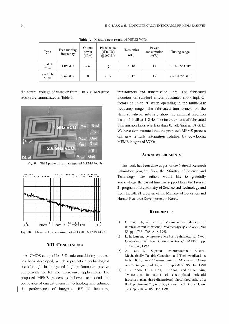
Fig. 5. Fabricated 1:1 MEMS transformer We have achieved significant improvement in
transformer performance by employing the metal surface micromachining process previously reported by our group [9,10]. This process provides an air-gap in the micromachined transformers to significantly reduce the substrate coupling loss and utilizes thick metal layers (>10 µm) to reduce ohmic loss. We have also achieved a high magnetic coupling factor (<0.81) in the fabricated spiral-type transformers as shown in Fig. 5. Fig. 6 shows the measured and modeled characteristics of the spiral type transformer in the frequency range from 0.05 to 10GHz, presenting the minimal insertion loss (S21) of 1.9dB at 1GHz. The S21 in Fig. 6 has a sharp null around 7GHz. This results from coupling capacitance between the primary and secondary coils [7],[11].
V. FULLY-INTEGRATED VCO USING MEMS INDUCTORS
Generally, planar transmission line structures are used in monolithic microwave integrated circuits for
JOURNAL OF SEMICONDUCTOR TECHNOLOGY AND SCIENCE, VOL.2, NO. 1, MARCH, 2002
53
flexibility and simplicity. It is important to develop low loss transmission lines to be used as resonators or filters when operating at microwave frequencies. In conventional silicon IC technologies, planar transmission lines suffer from metal and substrate loss [12]. To reduce metal resistance wide metal lines have to be used, however, this causes large substrate coupling losses. Therefore, thicker metal with less substrate coupling is key in obtaining lower loss transmission lines.
0 2 4 6 8 10
-40
-30
-20
-10
0
Frequency(GHz)
S21(
dB)
-30
-20
-10
0
Measured
ModeledS11(dB)
Fig. 6. Measured and modeled S-parameters of fabricated MEMS transformer
Fig. 7. Fabricated coplanar waveguide type MEMS transmission line
We have designed and developed MEMS transmission
lines using numerical analysis and a 3-D MEMS process. The fabricated coplanar waveguide, which we developed, is shown in Fig. 7. The signal line thickness is 15 µm, it has a width of 25 µm, a gap to the ground line of 10 µm, and a gap to the substrate of 40 µm. Fig. 8 shows the measured characteristics of the spiral type transformer in
the frequency range from 0.5 to 18 GHz. Measured insertion loss (S21) is less than 0.1 dB/mm and the phase discrepancy between the measured and simulated result is less than 1° at 18 GHz.
Freq (500.0MHz to 18.00GHz)
m1freq=1.800E10HzS21=0.988 / -26.923impedance = Z0 * (0.110 - j4.175)
m1
m2freq=1.800E10HzS11=0.013 / -159.771impedance = Z0 * (0.977 - j0.009)
m2
S21S11
Freq (500.0MHz to 18.00GHz)
m1freq=1.800E10HzS21=0.988 / -26.923impedance = Z0 * (0.110 - j4.175)
m1freq=1.800E10HzS21=0.988 / -26.923impedance = Z0 * (0.110 - j4.175)
m1
m2freq=1.800E10HzS11=0.013 / -159.771impedance = Z0 * (0.977 - j0.009)
m2freq=1.800E10HzS11=0.013 / -159.771impedance = Z0 * (0.977 - j0.009)
m2
S21S11
Fig. 8. Measured Smith chart plot of the MEMS transmission line
VI. FULLY-INTEGRATED VCO USING MEMS INDUCTORS
Voltage controlled oscillator (VCO) is one component which remains external to chips due to its stringent phase noise requirements. Phase noise is a measure of the signal purity of an oscillator and it decreases inversely proportional to square of the quality factor of the resonator. It is difficult to achieve a high quality factor in resonators, because, inductors with high quality factors are not available in the standard silicon process. 3-D MEMS inductors could overcome the high phase noise level in the standard process and give an integrated solution.
A fully integrated VCO, operating at 1 GHz and 2.6 GHz, has now been realized in a 0.18 µm TSMC and post-CMOS MEMS process. The active chip has been integrated with a MEMS inductor using the 3-D MEMS process. The integrated VCOs are shown in Fig. 9. The phase noise of the VCO has been measured, as shown in Fig. 10, using an HP8564E spectrum analyzer. The VCOs consume 15 mW from a 3 V power supply in the VCO core. The VCO tuning was measured by varying
E. C. PARK et al. : MONOLITHICALLY INTEGRABLE RF MEMS PASSIVES 54
the control voltage of varactor from 0 to 3 V. Measured results are summarized in Table 1.
1 GHz VCO
2.6 GHz VCO
1 GHz VCO
2.6 GHz VCO
Fig. 9. SEM photo of fully integrated MEMS VCOs
Fig. 10. Measured phase noise plot of 1 GHz MEMS VCO.
VII. CONCLUSIONS
A CMOS-compatible 3-D micromachining process has been developed, which represents a technological breakthrough in integrated high-performance passive components for RF and microwave applications. The proposed MEMS process is believed to extend the boundaries of current planar IC technology and enhance the performance of integrated RF IC inductors,
transformers and transmission lines. The fabricated inductors on standard silicon substrates show high Q-factors of up to 70 when operating in the multi-GHz frequency range. The fabricated transformers on the standard silicon substrate show the minimal insertion loss of 1.9 dB at 1 GHz. The insertion loss of fabricated transmission lines was less than 0.1 dB/mm at 18 GHz. We have demonstrated that the proposed MEMS process can give a fully integration solution by developing MEMS integrated VCOs.
ACKNOWLEDGMENTS
This work has been done as part of the National Research Laboratory program from the Ministry of Science and Technology. The authors would like to gratefully acknowledge the partial financial support from the Frontier 21 program of the Ministry of Science and Technology and from the BK 21 program of the Ministry of Education and Human Resource Development in Korea.
REFERENCES
[1] C. T.-C. Nguyen, et al., “Micromachined devices for wireless communications,” Proceedings of The IEEE, vol. 86, pp. 1756-1768, Aug. 1998.
[2] L. E. Larson, “Microwave MEMS Technology for Next-Generation Wireless Communications,” MTT-S, pp. 1073-1076, 1999.
[3] A. Dec, K. Suyama, “Micromachined Electro-Mechanically Tunable Capacitors and Their Applications to RF IC’s,” IEEE Transactions on Microwave Theory and Techniques, vol. 46, no. 12, pp.2587-2596, Dec. 1998.
[4] J.-B. Yoon, C.-H. Han, E. Yoon, and C.-K. Kim, “Monolithic fabrication of electroplated solenoid inductors using three-dimensional photolithography of a thick photoresist,” Jpn. J. Appl. Phys., vol. 37, pt. 1, no. 12B, pp. 7081-7085, Dec. 1998.
Table 1. Measurement results of MEMS VCOs
Type Free running frequency
Output power (dBm)
Phase noise (dBc/Hz) @300kHz
Harmonics (dB)
Power consumution
(mW) Tuning range
1 GHz VCO 1.08GHz -4.83 -124 < -18 15 1.08-1.83 GHz
2.6 GHz VCO 2.62GHz 0 -117 < -17 15 2.62~4.22 GHz
JOURNAL OF SEMICONDUCTOR TECHNOLOGY AND SCIENCE, VOL.2, NO. 1, MARCH, 2002
55
[5] J.-B. Yoon, B.-I. Kim, Y.-S. Choi, and E. Yoon, “3-D Lithography and Metal Surface Micromachining for RF and Microwave MEMS,” IEEE Int. MEMS Conf. Tech. Dig., pp. 673-676, Jan. 2002.
[6] J.-B. Yoon, Y.-S. Choi, B.-I. Kim, Y. Eo, and E. Yoon, “CMOS-compatible, surface micromachined, suspended spiral inductors and their proper model for multi-GHz silicon RF IC’s,” submitted to IEEE Electron Device Lett.
[7] J. R. Long, “ Monolithic Transformer for Silicon RF IC Design,” IEEE J. Solid-State Circuits, vol. 35, pp. 1368-1382, Sep. 2000.
[8] J. Hartung, “Integrated Passive Components in MCM-Si Technology and their Application in RF-Systems,” Int.Conf. on Multichip Modules and High Density Packaging, pp. 256-261, 1998.
[9] J.-B. Yoon, C.-H. Han, E. Yoon and C.-K. Kim, “Monolithic Integration of 3-D Electoplated Microstructures of Unlimited Number of Levels Using Planarization With a Sacrificial Metallic Mold (PSMM),” IEEE MEMS ’99 Tech. Dig., pp.624-629, Jan. 1999.
[10] Y.-S. Choi, J.-B. Yoon, B.-I. Kim, Y. Eo, and E. Yoon, “A High-Performance MEMS Transformer for Silicon RF ICs,” IEEE Int. MEMS Conf. Tech. Dig., pp. 653-656, Jan. 2002.
[11] Y.-J, Kim, Mark G. Allen, “Surface Micromachined Solenoid Inductors for High Frequency Applications,” IEEE. Trans. Components, packaging, and manufacturing Tech., Part C, vol.21, No.1, Jan. 1998
[12] B. Kleveland, et al., “Exploiting CMOS Reverse Interconnect Scaling in Multigigahertz Amplifier and Oscillator Design,” IEEE Journal of Solid-State Circuits, vol. 36, No. 10, Oct. 2001.
Eun-Chul Park was born in Taegu, Korea. He received the B.S. degree in electronic engineering from Kyungpook National University in 1996 and the M.S. degree in electrical engineering from Korea Advanced Institute of Science and Technology (KAIST), Taejon, Korea in 1998. He is presently pursing the Ph.D. degree at KAIST. His
present interest is in the Integrated MEMS RF module. Currently his work focuses on high performance VCOs for RF and microwave applications using MEMS structures.
Yun-Seok Choi was born in Pusan, Korea. He received the B.S degree in electronics engineering from Pusan National University in 1997 and the M.S degree in Electrical Engineering from Korea Advanced Institute of Science and Technology (KAIST), Taejon, Korea, in 1999. Since 1999, he has been working toward the Ph.D. degree at the same
university. His research interests include the fabrication and modeling of
RF passive components.
Jun-Bo Yoon received the B.S. (Summa Cum Laude), M.S., and Ph.D. degrees all in Electrical Engineering from Korea Advanced Institute of Science and Technology (KAIST), Taejon, Korea, in 1993, 1995, and 1999, respectively. His doctoral research was engaged in the development of the three-dimensional
microstructure technology for microfluidic systems and integrated inductors. From 1999 to 2000, he was with the University of Michigan, Ann Arbor, MI, as a Postdoctoral Research Fellow, where he invented a tunable micromechanical capacitor featuring movable dielectric for RF applications. In 2000, he came back to the Department of Electrical Engineering at KAIST, where he is currently a Research Assistant Professor. He has been involved in the development of a single-crystal-silicon transmissive AMLCD using bulk micromachining, a monolithic thermal inkjet printhead, a surface-micromachined microgyroscope, and micromachined integrated inductors. His research interests include microfabrication & nanofabrication (3-D microstructure & nanostructure) technologies, micro/nano sensors and actuators, optical-MEMS, bio-MEMS, and RF/microwave MEMS. Dr. Yoon is a Member of the IEEE and received the third-place award at the IEEE MTT-S International Microwave Symposium Student Paper Competition in June 1999.
Euisik Yoon was born in Seoul, Korea. He received the B.S. and M.S. degrees in electronic engineering from Seoul National University in 1982 and 1984, respectively, and a Ph.D. degree in electrical engineering from the University of Michigan, Ann Arbor, in 1990. From 1990 to 1994 he was with the Fairchild
Research Center of the National Semiconductor Corp., Santa Clara, CA, where he was engaged in researches on deep submicron CMOS integration and advanced gate dielectrics. From 1994 to 1996, he was a Member of the technical staff at Silicon Graphics Inc., Mountain View, CA, working on the design of the MIPS microprocessor R4300i and the RCP 3-D graphic coprocessor. In 1996 he joined the Department of Electrical Engineering at Korea Advanced Institute of Science and Technology (KAIST), Daejon, Korea, where he is now an associate professor. His present research interests are in microsensors, integrated microsystems, and VLSI circuit design.


![On an integrable discretisation of the Lotka-Volterra system · all conserved quantities of the integrable system. This problem prompts a concept called integrable discretization[1].](https://static.fdocuments.in/doc/165x107/5f0ea3b77e708231d4403581/on-an-integrable-discretisation-of-the-lotka-volterra-all-conserved-quantities-of.jpg)