9 Vlsicad Placer
83
VLSI CAD: Logic to Layout Rob A. Rutenbar University of Illinois Lecture 9.1 ASIC Placement: Basics
description
vlsi
Transcript of 9 Vlsicad Placer
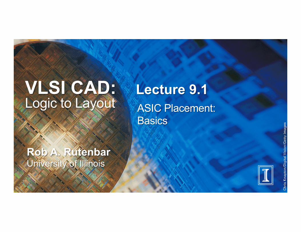
VLSI CAD: Logic to Layout
Rob A. Rutenbar University of Illinois
Lecture 9.1 ASIC Placement: Basics
© 2013, R.A. Rutenbar
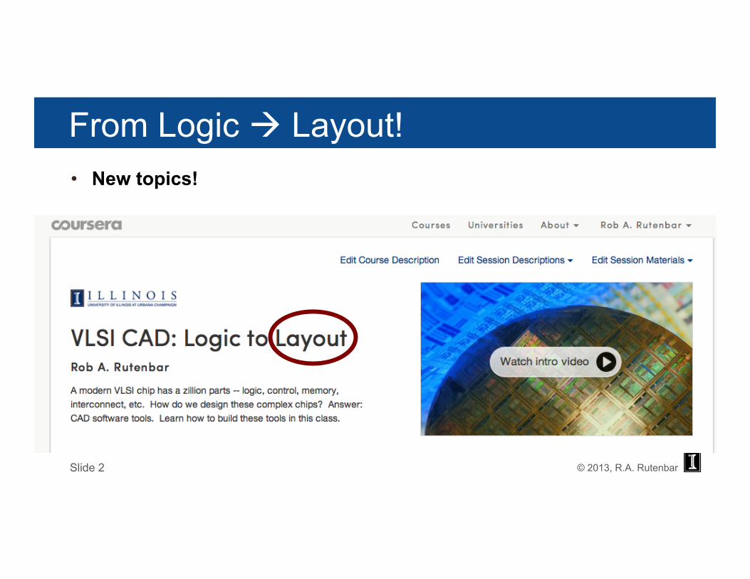
From Logic à Layout! • New topics!
Slide 2
© 2013, R.A. Rutenbar
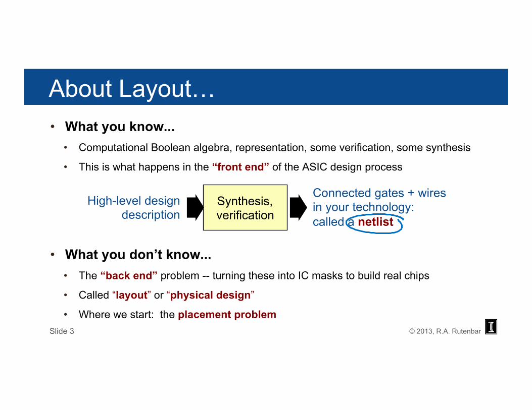
About Layout… • What you know...
• Computational Boolean algebra, representation, some verification, some synthesis
• This is what happens in the “front end” of the ASIC design process
• What you don’t know... • The “back end” problem -- turning these into IC masks to build real chips
• Called “layout” or “physical design”
• Where we start: the placement problem
Synthesis, verification
Connected gates + wires in your technology: called a netlist
High-level design description
Slide 3
© 2013, R.A. Rutenbar
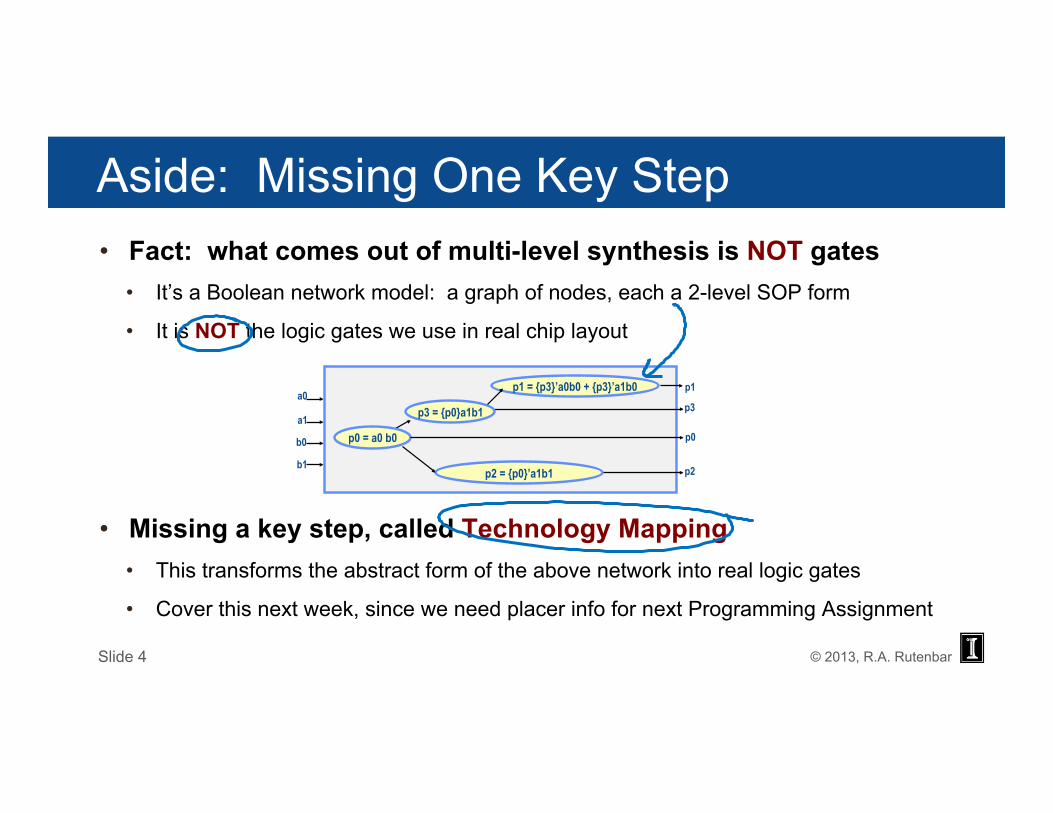
Aside: Missing One Key Step • Fact: what comes out of multi-level synthesis is NOT gates
• It’s a Boolean network model: a graph of nodes, each a 2-level SOP form
• It is NOT the logic gates we use in real chip layout
• Missing a key step, called Technology Mapping • This transforms the abstract form of the above network into real logic gates
• Cover this next week, since we need placer info for next Programming Assignment
Slide 4
p0
p3 a0
b0
a1
b1
p0 = a0 b0
p1 = {p3}’a0b0 + {p3}’a1b0
p2 = {p0}’a1b1
p3 = {p0}a1b1
p1
p2
© 2013, R.A. Rutenbar
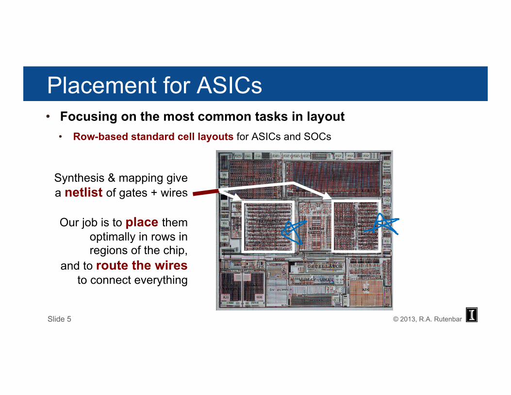
Placement for ASICs • Focusing on the most common tasks in layout
• Row-based standard cell layouts for ASICs and SOCs
Synthesis & mapping give a netlist of gates + wires
Our job is to place them
optimally in rows in regions of the chip,
and to route the wires to connect everything
Slide 5
© 2013, R.A. Rutenbar
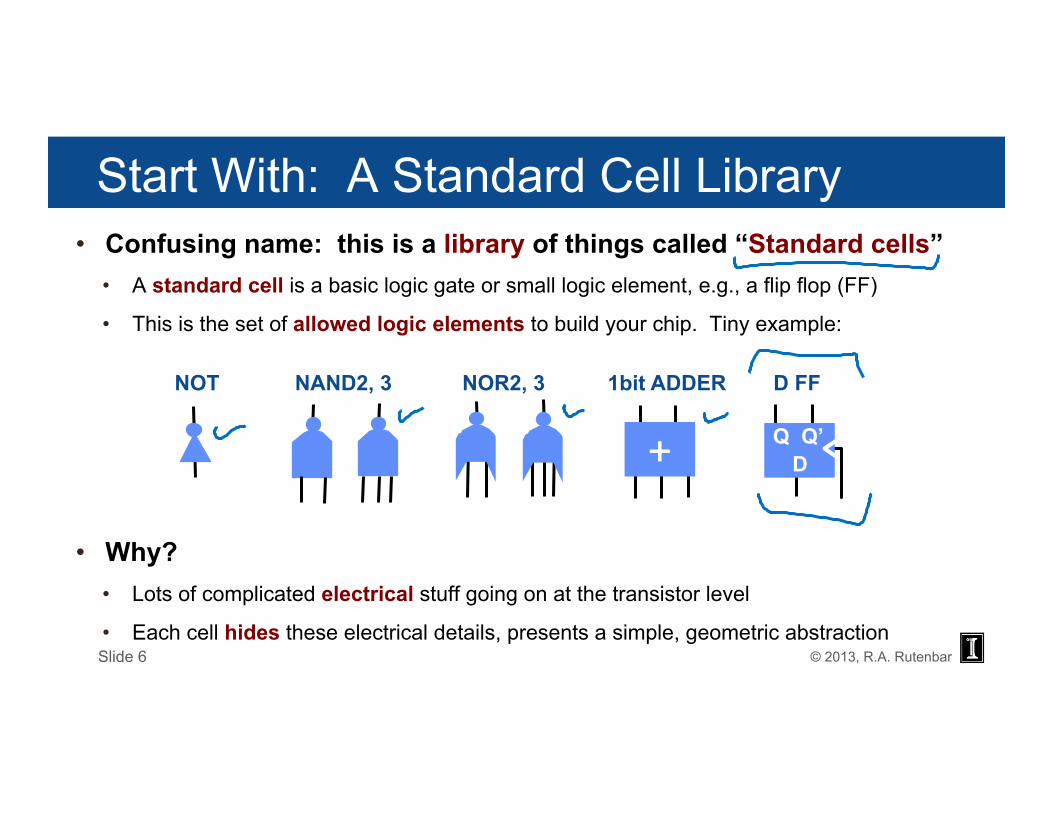
Start With: A Standard Cell Library • Confusing name: this is a library of things called “Standard cells”
• A standard cell is a basic logic gate or small logic element, e.g., a flip flop (FF)
• This is the set of allowed logic elements to build your chip. Tiny example:
• Why? • Lots of complicated electrical stuff going on at the transistor level
• Each cell hides these electrical details, presents a simple, geometric abstraction
NOT NAND2, 3 NOR2, 3
+ D
1bit ADDER D FF
Q Q’
Slide 6
© 2013, R.A. Rutenbar
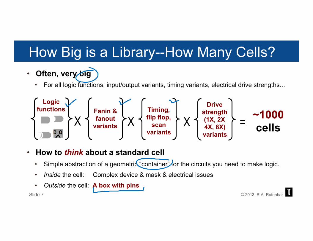
How Big is a Library--How Many Cells? • Often, very big
• For all logic functions, input/output variants, timing variants, electrical drive strengths…
• How to think about a standard cell • Simple abstraction of a geometric “container” for the circuits you need to make logic.
• Inside the cell: Complex device & mask & electrical issues
• Outside the cell: A box with pins
X Fanin & fanout
variants X Timing, flip flop,
scan variants
X
Drive strength (1X, 2X 4X, 8X) variants
= ~1000 cells
Logic functions
Slide 7
© 2013, R.A. Rutenbar
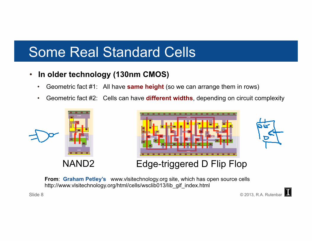
Some Real Standard Cells • In older technology (130nm CMOS)
• Geometric fact #1: All have same height (so we can arrange them in rows)
• Geometric fact #2: Cells can have different widths, depending on circuit complexity
From: Graham Petley’s www.vlsitechnology.org site, which has open source cells http://www.vlsitechnology.org/html/cells/wsclib013/lib_gif_index.html
NAND2 Edge-triggered D Flip Flop
Slide 8
© 2013, R.A. Rutenbar
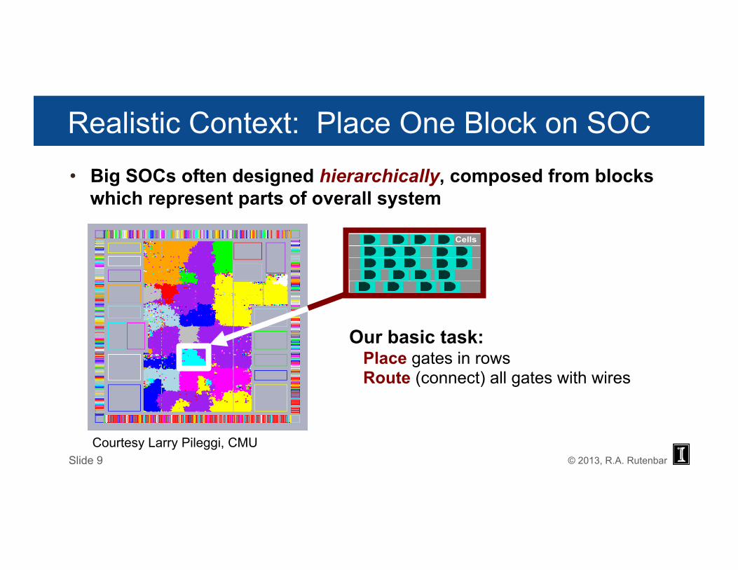
Realistic Context: Place One Block on SOC • Big SOCs often designed hierarchically, composed from blocks
which represent parts of overall system
Courtesy Larry Pileggi, CMU
CellsCells
Our basic task: Place gates in rows Route (connect) all gates with wires
Slide 9
© 2013, R.A. Rutenbar
0"
5000"
10000"
15000"
20000"
25000"
30000"
1" 2" 3" 4" 5" 6" 7" 8" 9" 10"
11"
12"
13"
14"
15"
16"
17"
18"
19"
20"
21,30"
31,50"
51,100"
100,123"
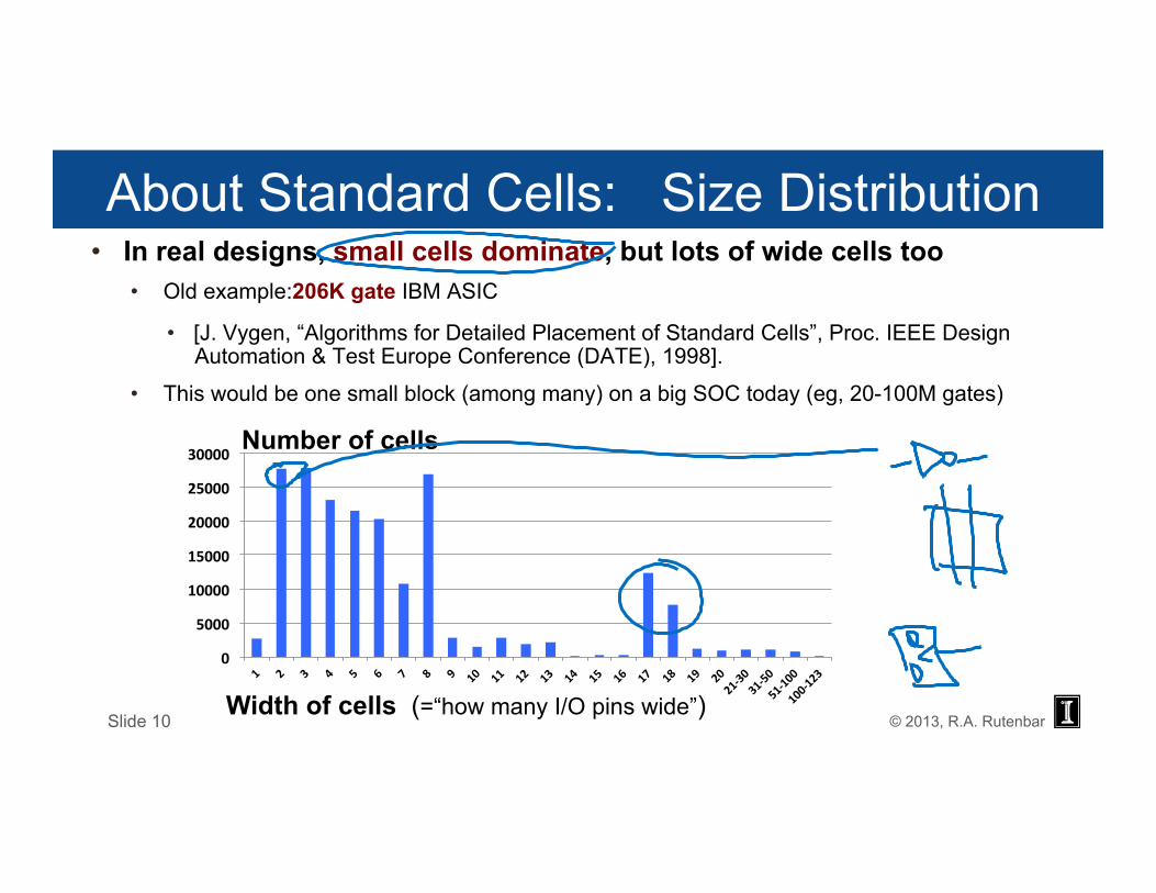
About Standard Cells: Size Distribution • In real designs, small cells dominate, but lots of wide cells too
• Old example:206K gate IBM ASIC
• [J. Vygen, “Algorithms for Detailed Placement of Standard Cells”, Proc. IEEE Design Automation & Test Europe Conference (DATE), 1998].
• This would be one small block (among many) on a big SOC today (eg, 20-100M gates)
Number of cells
Width of cells (=“how many I/O pins wide”) Slide 10
© 2013, R.A. Rutenbar
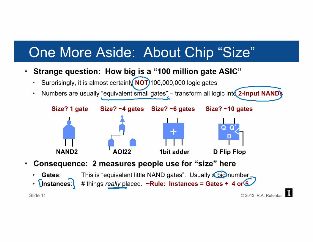
One More Aside: About Chip “Size” • Strange question: How big is a “100 million gate ASIC”
• Surprisingly, it is almost certainly NOT 100,000,000 logic gates
• Numbers are usually “equivalent small gates” – transform all logic into 2-input NANDs
• Consequence: 2 measures people use for “size” here
• Gates: This is “equivalent little NAND gates”. Usually a big number • Instances: # things really placed. ~Rule: Instances = Gates ÷ 4 or 5
Size? 1 gate
+
D Flip Flop
Q Q’
Size? ~6 gates
NAND2 1bit adder
Size? ~10 gates
AOI22
Size? ~4 gates
D
Slide 11
© 2013, R.A. Rutenbar
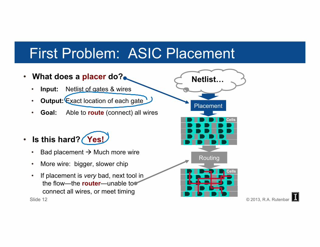
First Problem: ASIC Placement • What does a placer do?
• Input: Netlist of gates & wires
• Output: Exact location of each gate
• Goal: Able to route (connect) all wires
• Is this hard? Yes! • Bad placement à Much more wire
• More wire: bigger, slower chip
• If placement is very bad, next tool in the flow—the router—unable to connect all wires, or meet timing
Netlist…
Placement
CellsCells
CellsCells
Routing
Slide 12

VLSI CAD: Logic to Layout
Rob A. Rutenbar University of Illinois
Lecture 9.2 ASIC Placement: Wirelength Estimation
© 2013, R.A. Rutenbar
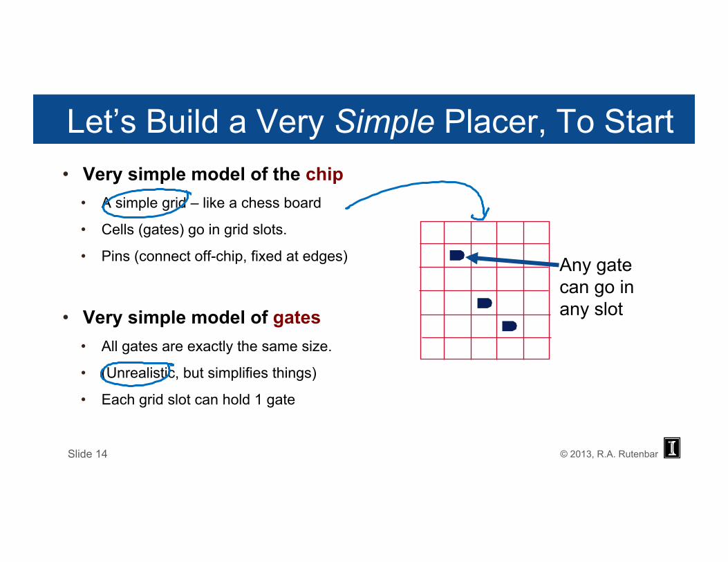
Let’s Build a Very Simple Placer, To Start • Very simple model of the chip
• A simple grid – like a chess board
• Cells (gates) go in grid slots.
• Pins (connect off-chip, fixed at edges)
• Very simple model of gates • All gates are exactly the same size.
• (Unrealistic, but simplifies things)
• Each grid slot can hold 1 gate
Any gate can go in any slot
Slide 14
© 2013, R.A. Rutenbar
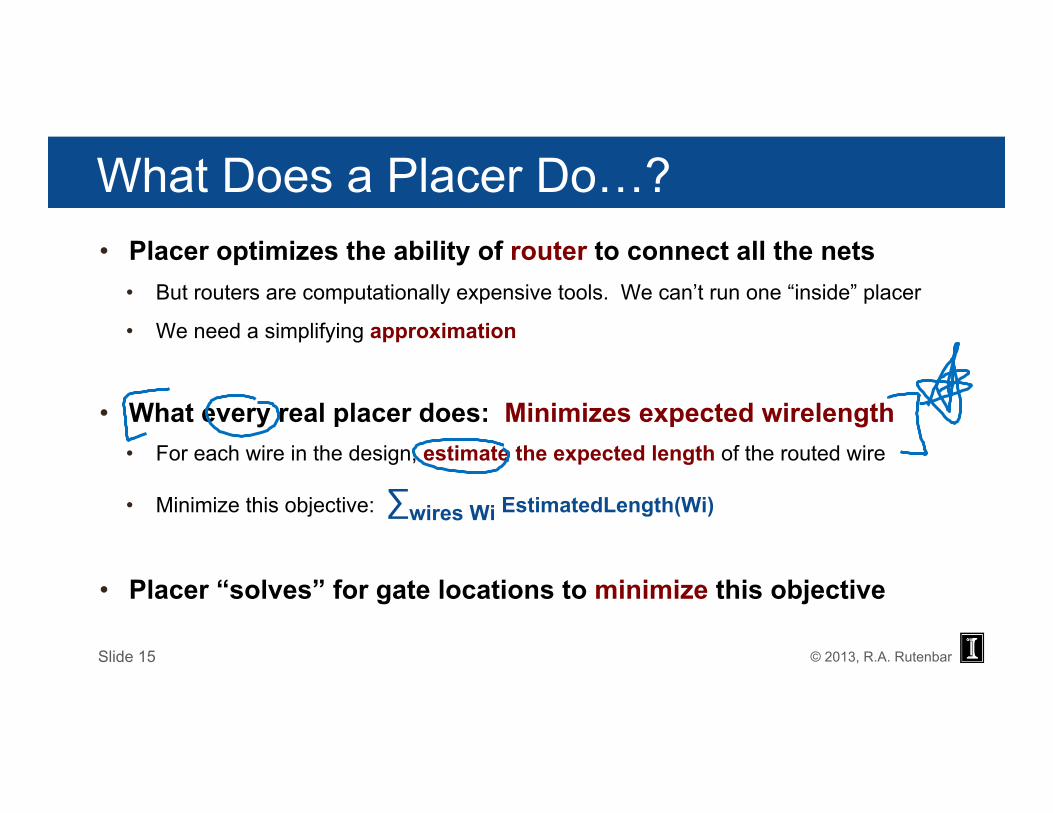
What Does a Placer Do…? • Placer optimizes the ability of router to connect all the nets
• But routers are computationally expensive tools. We can’t run one “inside” placer
• We need a simplifying approximation
• What every real placer does: Minimizes expected wirelength • For each wire in the design, estimate the expected length of the routed wire
• Minimize this objective: ∑wires Wi EstimatedLength(Wi)
• Placer “solves” for gate locations to minimize this objective
Slide 15
© 2013, R.A. Rutenbar
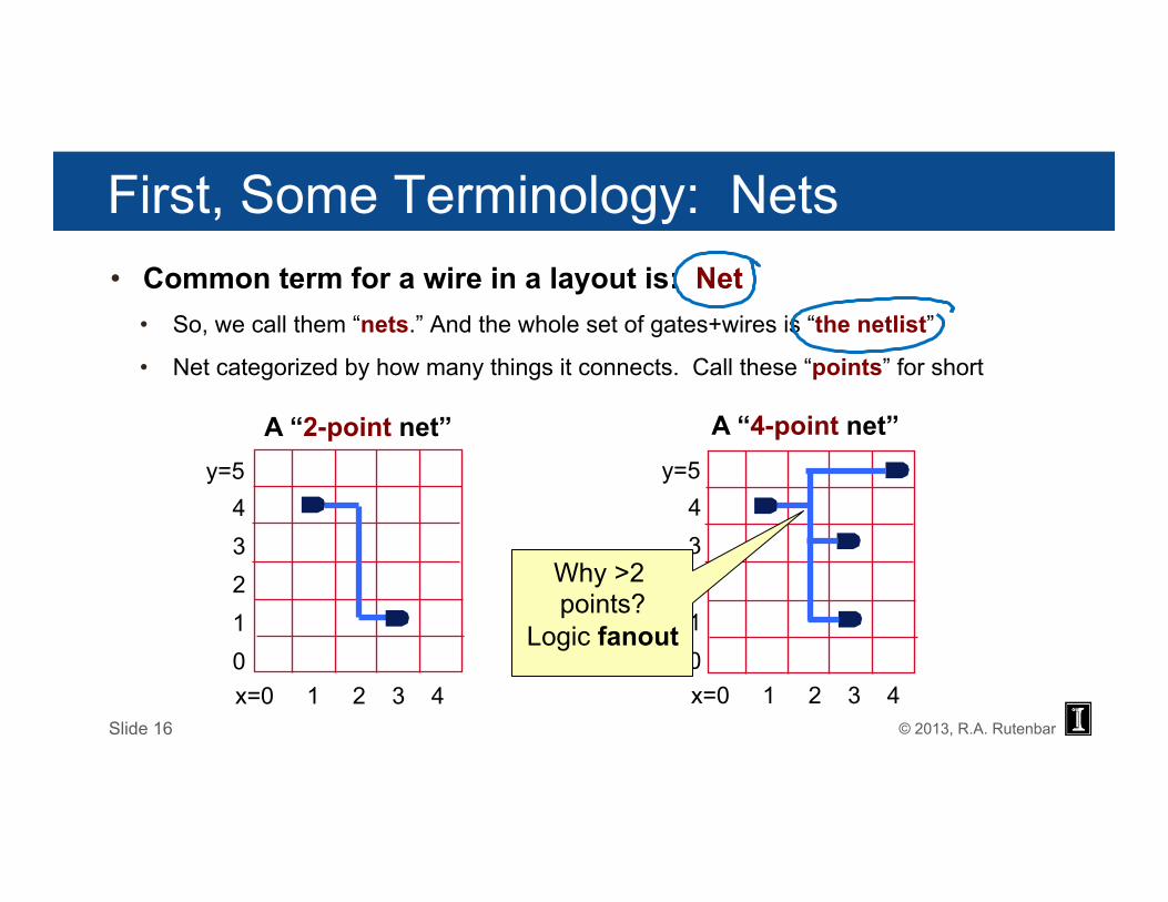
First, Some Terminology: Nets • Common term for a wire in a layout is: Net
• So, we call them “nets.” And the whole set of gates+wires is “the netlist”
• Net categorized by how many things it connects. Call these “points” for short
Slide 16
x=0 1 2 3 4
y=5 4 3 2 1 0
A “2-point net”
x=0 1 2 3 4
y=5 4 3 2 1 0
A “4-point net”
Why >2 points?
Logic fanout
© 2013, R.A. Rutenbar
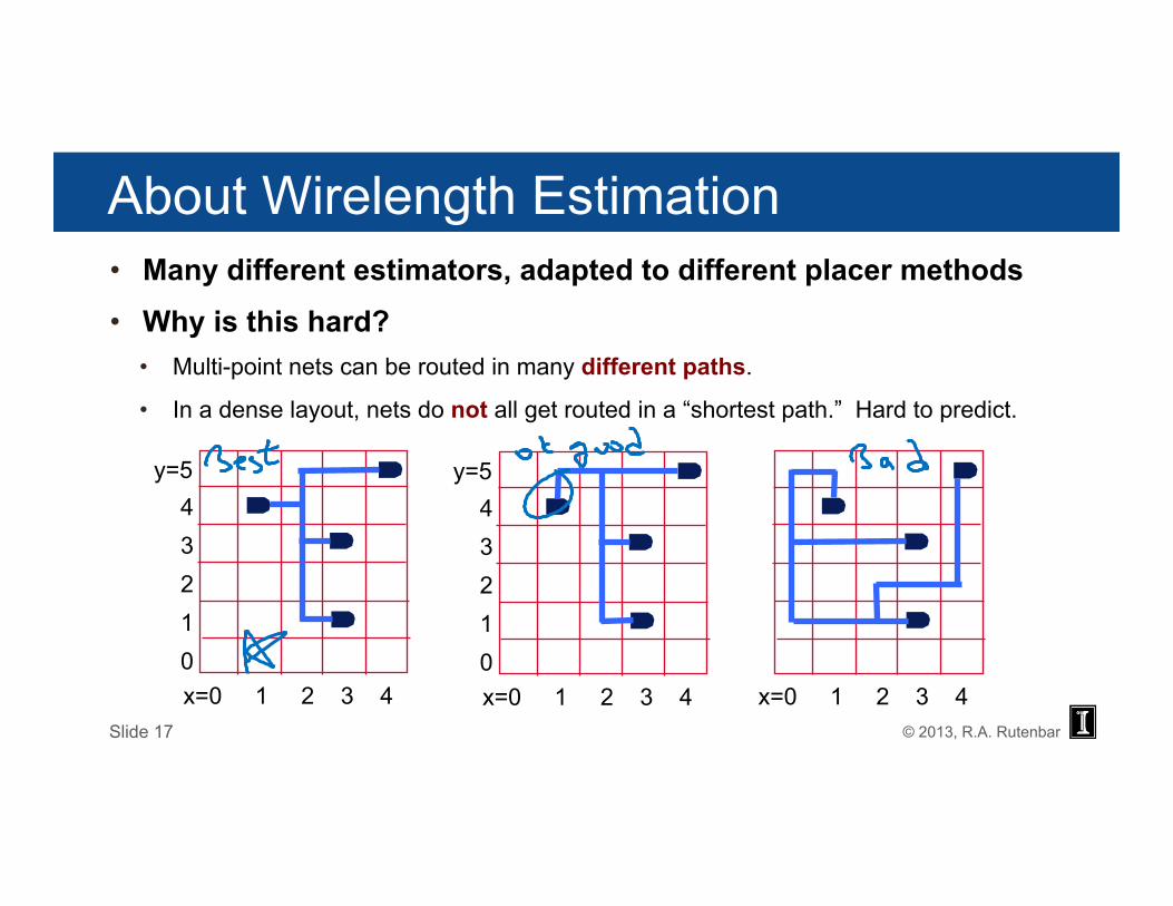
About Wirelength Estimation • Many different estimators, adapted to different placer methods • Why is this hard?
• Multi-point nets can be routed in many different paths.
• In a dense layout, nets do not all get routed in a “shortest path.” Hard to predict.
Slide 17
x=0 1 2 3 4
y=5 4 3 2 1 0
x=0 1 2 3 4 x=0 1 2 3 4
y=5 4 3 2 1 0
© 2013, R.A. Rutenbar
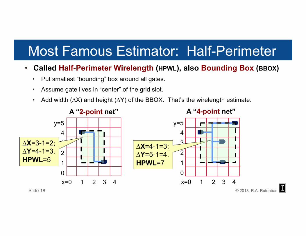
Most Famous Estimator: Half-Perimeter • Called Half-Perimeter Wirelength (HPWL), also Bounding Box (BBOX)
• Put smallest “bounding” box around all gates.
• Assume gate lives in “center” of the grid slot.
• Add width (∆X) and height (∆Y) of the BBOX. That’s the wirelength estimate.
Slide 18
x=0 1 2 3 4
y=5 4 3 2 1 0
x=0 1 2 3 4
y=5 4 3 2 1 0
A “4-point net”
∆X=3-1=2; ∆Y=4-1=3. HPWL=5
∆X=4-1=3; ∆Y=5-1=4. HPWL=7
A “2-point net”

© 2013, R.A. Rutenbar
About HPWL Estimator • Easy to calculate, even for a multi-point net
• General formula:
• HPWL = [max{X coordinates of all gates) – min{X coordinates of all gates}] + [max{Y coordinates of all gates) – min{Y coordinates of all gates}]
• Always a lower bound on the real wire length • No matter how complex the final routed wire path is…
• …you need at least this much wire to connect everything.
• Aside: all wiring on big chips (and most wire on boards) is strictly horizontal & vertical – no “arbitrary angles” for manufacturing reasons.
• Another reason HPWL is a good estimator.
Slide 19
© 2013, R.A. Rutenbar
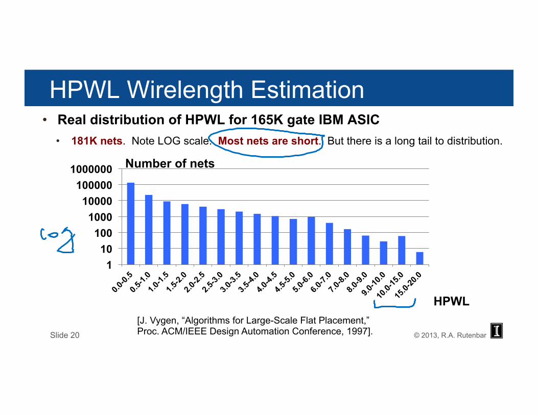
HPWL Wirelength Estimation • Real distribution of HPWL for 165K gate IBM ASIC
• 181K nets. Note LOG scale. Most nets are short. But there is a long tail to distribution.
Number of nets
1 10
100 1000
10000 100000
1000000
HPWL
Slide 20
[J. Vygen, “Algorithms for Large-Scale Flat Placement,” Proc. ACM/IEEE Design Automation Conference, 1997].
VLSI CAD: Logic to Layout
Rob A. Rutenbar University of Illinois
Lecture 9.3 ASIC Placement: Simple Iterative Improvement Placement
© 2013, R.A. Rutenbar
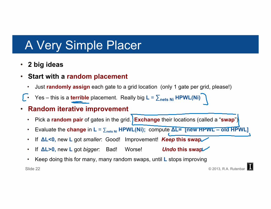
A Very Simple Placer • 2 big ideas • Start with a random placement
• Just randomly assign each gate to a grid location (only 1 gate per grid, please!)
• Yes – this is a terrible placement. Really big L = ∑nets Ni HPWL(Ni)
• Random iterative improvement • Pick a random pair of gates in the grid. Exchange their locations (called a “swap”)
• Evaluate the change in L = ∑nets Ni HPWL(Ni); compute ΔL= [new HPWL – old HPWL]
• If ΔL<0, new L got smaller: Good! Improvement! Keep this swap
• If ΔL>0, new L got bigger: Bad! Worse! Undo this swap
• Keep doing this for many, many random swaps, until L stops improving Slide 22
© 2013, R.A. Rutenbar
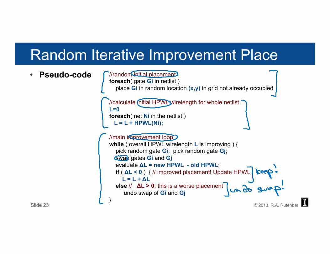
Random Iterative Improvement Place • Pseudo-code
Slide 23
//random initial placement foreach( gate Gi in netlist ) place Gi in random location (x,y) in grid not already occupied //calculate initial HPWL wirelength for whole netlist L=0 foreach( net Ni in the netlist ) L = L + HPWL(Ni); //main improvement loop while ( overall HPWL wirelength L is improving ) { pick random gate Gi; pick random gate Gj; swap gates Gi and Gj evaluate ΔL = new HPWL - old HPWL; if ( ΔL < 0 ) { // improved placement! Update HPWL L = L + ΔL else // ΔL > 0, this is a worse placement undo swap of Gi and Gj }
© 2013, R.A. Rutenbar
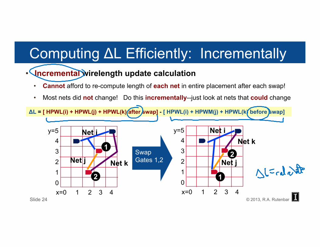
Computing ΔL Efficiently: Incrementally • Incremental wirelength update calculation
• Cannot afford to re-compute length of each net in entire placement after each swap!
• Most nets did not change! Do this incrementally--just look at nets that could change
ΔL = [ HPWL(i) + HPWL(j) + HPWL(k) after swap] - [ HPWL(i) + HPWM(j) + HPWL(k) before swap]
x=0 1 2 3 4
y=5 4 3 2 1 0
1
2
Swap Gates 1,2
Net i
Net j Net k
x=0 1 2 3 4
y=5 4 3 2 1 0
1
2
Net i
Net j
Net k
Slide 24
© 2013, R.A. Rutenbar
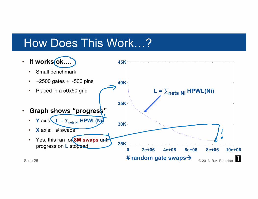
How Does This Work…? • It works ok….
• Small benchmark
• ~2500 gates + ~500 pins
• Placed in a 50x50 grid
• Graph shows “progress” • Y axis: L = ∑nets Ni HPWL(Ni)
• X axis: # swaps
• Yes, this ran for 8M swaps until progress on L stopped
Slide 25
0 2e+06 4e+06 6e+06 8e+06 10e+06 25K
30K
35K
40K
45K
L = ∑nets Ni HPWL(Ni)
# random gate swapsà
© 2013, R.A. Rutenbar
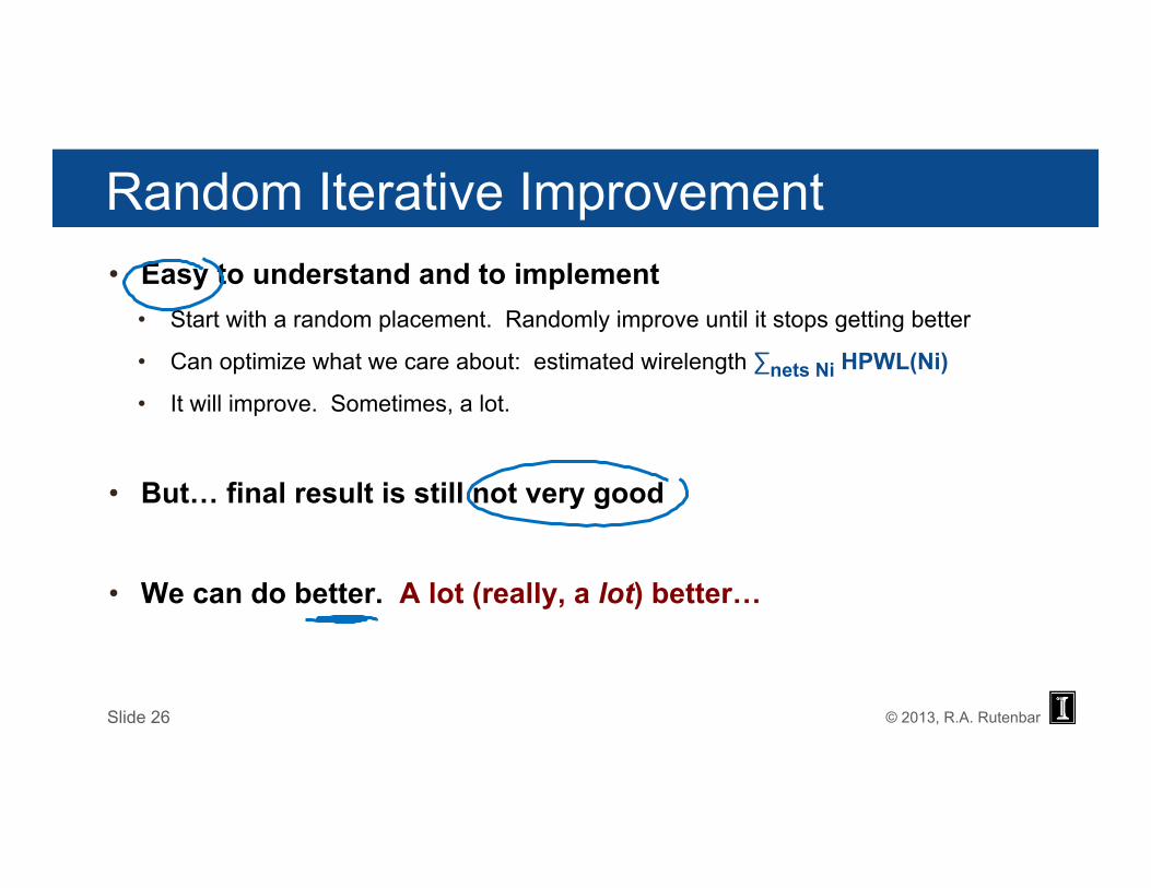
Random Iterative Improvement • Easy to understand and to implement
• Start with a random placement. Randomly improve until it stops getting better
• Can optimize what we care about: estimated wirelength ∑nets Ni HPWL(Ni)
• It will improve. Sometimes, a lot.
• But… final result is still not very good
• We can do better. A lot (really, a lot) better…
Slide 26
VLSI CAD: Logic to Layout
Rob A. Rutenbar University of Illinois
Lecture 9.4 ASIC Placement: Iterative Improvement With Hill-Climbing
© 2013, R.A. Rutenbar
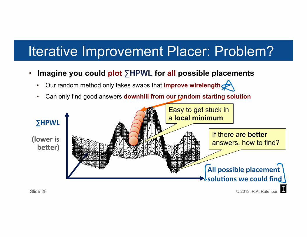
Iterative Improvement Placer: Problem? • Imagine you could plot ∑HPWL for all possible placements
• Our random method only takes swaps that improve wirelength
• Can only find good answers downhill from our random starting solution
Slide 28
∑HPWL
(lower is be0er)
All possible placement solu:ons we could find
Easy to get stuck in a local minimum
If there are better answers, how to find?
© 2013, R.A. Rutenbar
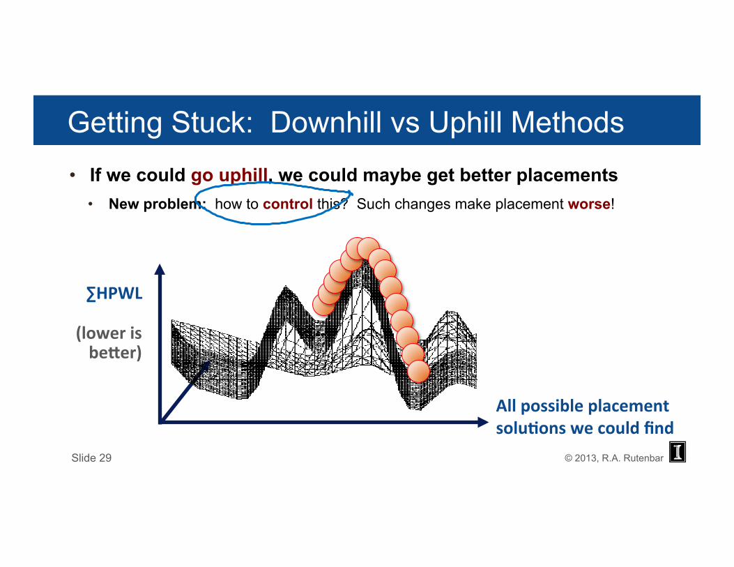
Getting Stuck: Downhill vs Uphill Methods • If we could go uphill, we could maybe get better placements
• New problem: how to control this? Such changes make placement worse!
Slide 29
∑HPWL
(lower is be0er)
All possible placement solu:ons we could find
© 2013, R.A. Rutenbar
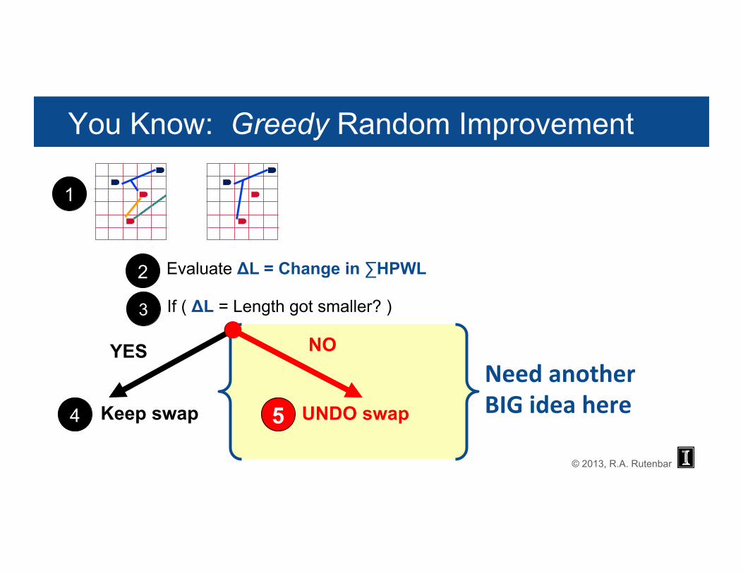
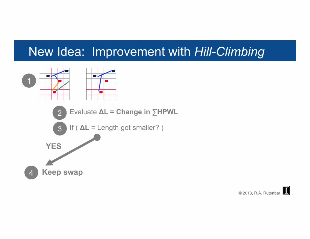
You Know: Greedy Random Improvement
1
3 If ( ΔL = Length got smaller? )
Evaluate ΔL = Change in ∑HPWL 2
4
YES
Keep swap
Need another BIG idea here 5
NO
UNDO swap
1
2 1
2Swap
Slide 30
© 2013, R.A. Rutenbar
New Idea: Improvement with Hill-Climbing
1
3 If ( ΔL = Length got smaller? )
Evaluate ΔL = Change in ∑HPWL 2
4
YES
Keep swap
1
2 1
2Swap
NO
5 Evaluate function P(ΔL, T) P = probability we accept swap Randomly keep “with probability P”
New: Hill-climbing control parameter, T=temperature
Slide 31
© 2013, R.A. Rutenbar
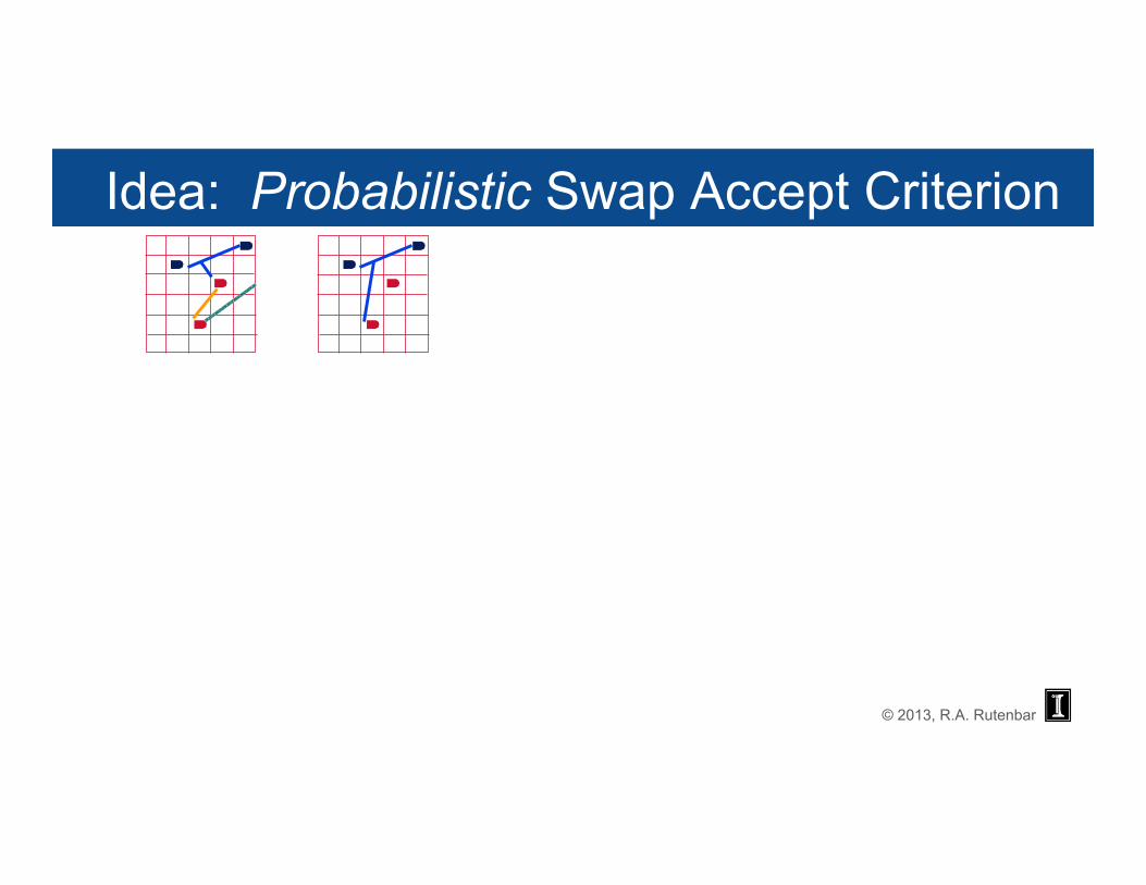
Idea: Probabilistic Swap Accept Criterion 1
2 1
2Swap
ΔL = Change in length = Longer (positive)
T e−ΔLT
…a probability P, like 0.72
R = uniform random number between 0 and 1
Slide 32
if (R < P) then Keep the swap else Undo the swap
© 2013, R.A. Rutenbar
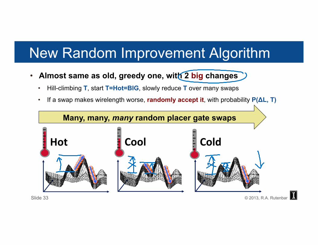
New Random Improvement Algorithm • Almost same as old, greedy one, with 2 big changes
• Hill-climbing T, start T=Hot=BIG, slowly reduce T over many swaps
• If a swap makes wirelength worse, randomly accept it, with probability P(ΔL, T)
Slide 33
Hot$ Cool$ Cold$
Many, many, many random placer gate swaps
Hot$ Cool$ Cold$Hot$ Cool$ Cold$

VLSI CAD: Logic to Layout
Rob A. Rutenbar University of Illinois
Lecture 9.5 ASIC Placement: Simulated Annealing Placement

© 2013, R.A. Rutenbar
New Famous Algorithm: Simulated Annealing • Almost same as old, greedy one, with 2 big changes
• Hill-climbing T, start T=Hot=BIG, slowly reduce T over many swaps
• If a swap makes wirelength worse, randomly accept it, with probability P(ΔL, T)
Slide 35
Hot$ Cool$ Cold$
Many, many, many random placer gate swaps
© 2013, R.A. Rutenbar
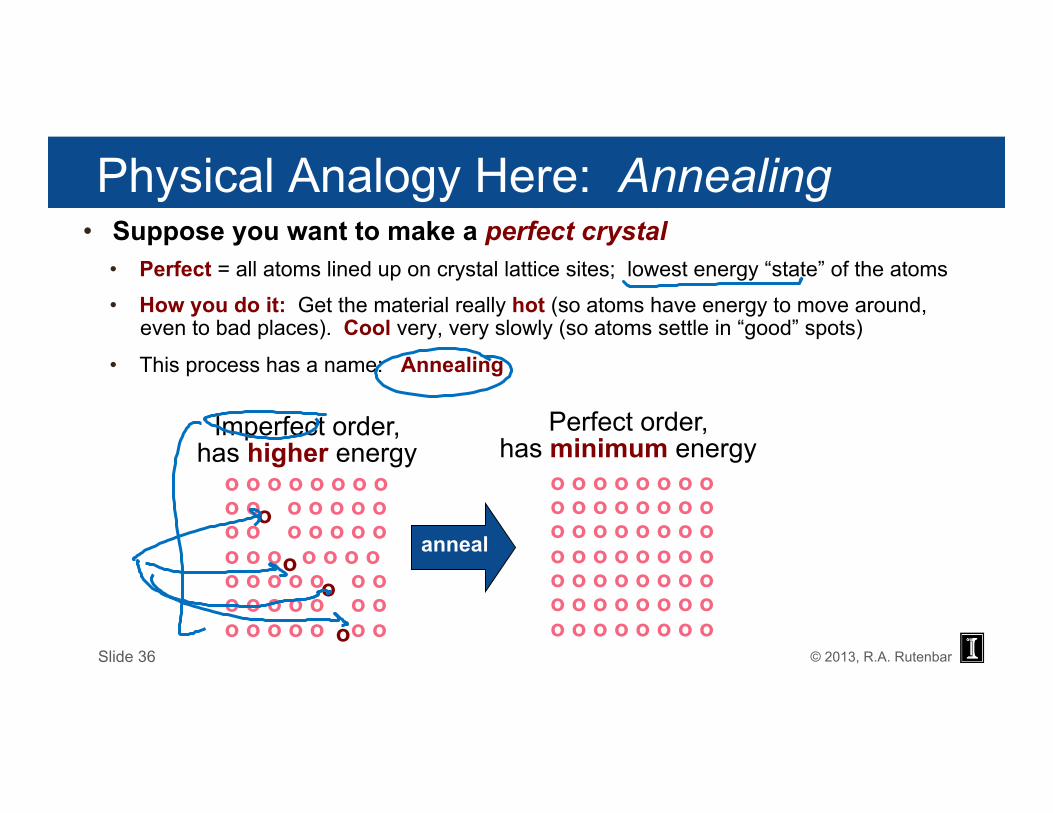
Physical Analogy Here: Annealing • Suppose you want to make a perfect crystal
• Perfect = all atoms lined up on crystal lattice sites; lowest energy “state” of the atoms
• How you do it: Get the material really hot (so atoms have energy to move around, even to bad places). Cool very, very slowly (so atoms settle in “good” spots)
• This process has a name: Annealing
Imperfect order, has higher energy
o o o o o o o o o o o o o o o o o o o o o o o o o o o o o o o o o o o o o o o o o o o o o o o o o o
o
o o
o Slide 36
Perfect order, has minimum energy
o o o o o o o o o o o o o o o o o o o o o o o o o o o o o o o o o o o o o o o o o o o o o o o o o o o o o o o o
anneal
© 2013, R.A. Rutenbar
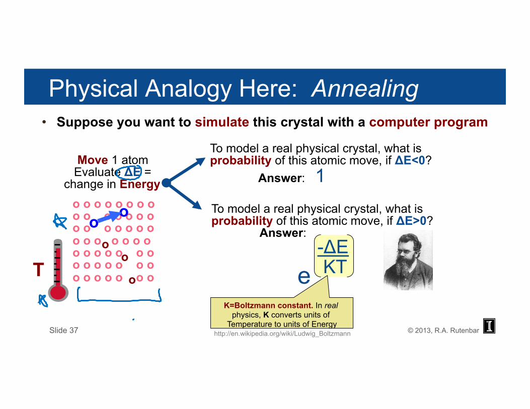
Physical Analogy Here: Annealing • Suppose you want to simulate this crystal with a computer program
Move 1 atom Evaluate ΔE =
change in Energy o o o o o o o o o o o o o o o o o o o o o o o o o o o o o o o o o o o o o o o o o o o o o o o o o o
o o
o
o
Slide 37
o
To model a real physical crystal, what is probability of this atomic move, if ΔE<0?
Answer: 1 To model a real physical crystal, what is probability of this atomic move, if ΔE>0?
Answer:
e -ΔE KT T
K=Boltzmann constant. In real physics, K converts units of
Temperature to units of Energy http://en.wikipedia.org/wiki/Ludwig_Boltzmann
© 2013, R.A. Rutenbar
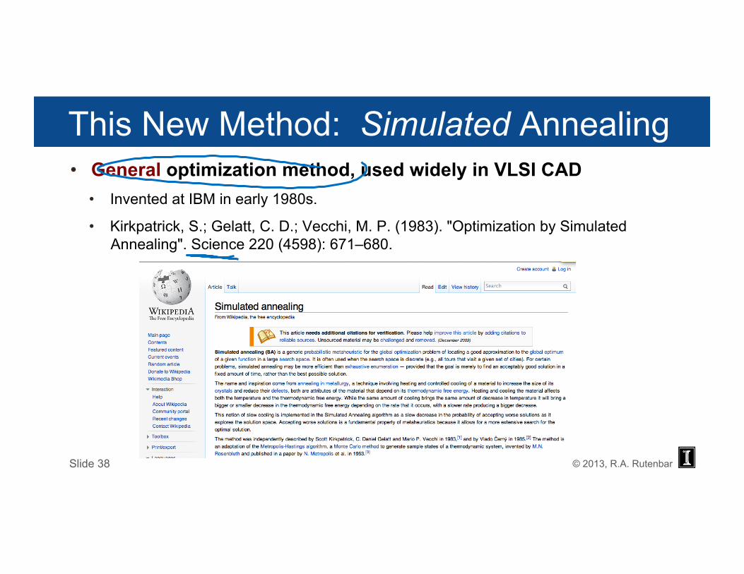
This New Method: Simulated Annealing • General optimization method, used widely in VLSI CAD
• Invented at IBM in early 1980s.
• Kirkpatrick, S.; Gelatt, C. D.; Vecchi, M. P. (1983). "Optimization by Simulated Annealing". Science 220 (4598): 671–680.
Slide 38

© 2013, R.A. Rutenbar
Start with a random initial placement with wirelength = ∑HPWL(net) T = temperature = hot; frozen = false; while ( ! frozen ) {
for (s=1; s< M* #gates in layout; s++) { // M is how many swaps-per-gate Swap 2 random gates Gi and Gj Compute ∆L = [∑HPWL(net) after swap] - [∑HPWL(net) before swap] if (∆L < 0 ) then accept this swap //this is a new, better placement else { if( uniform_random() < exp( -∆L/T ) ) then accept this ‘uphill’ swap //this is a new, worse placement else undo this ‘uphill’ swap } if (∑HPWL(net) still decreasing over the last few temperatures) then T = 0.9 * T // cool the temperature; do more gate swaps else frozen = true
} return (final placement as best solution)
Annealing Placer: Pseudo-code
New: Probabilistic swap accept
New: Annealing Temperature cooling “outer loop”
Slide 39
© 2013, R.A. Rutenbar
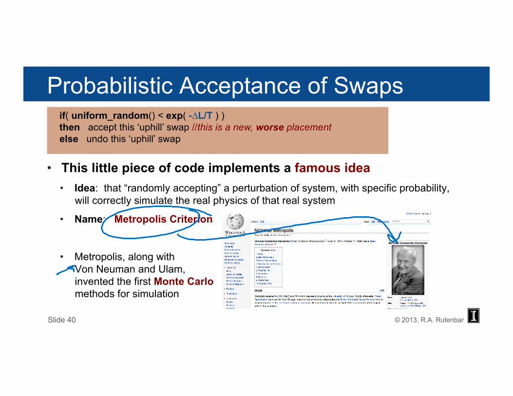
if( uniform_random() < exp( -∆L/T ) ) then accept this ‘uphill’ swap //this is a new, worse placement else undo this ‘uphill’ swap
Probabilistic Acceptance of Swaps
• This little piece of code implements a famous idea • Idea: that “randomly accepting” a perturbation of system, with specific probability,
will correctly simulate the real physics of that real system
• Name: Metropolis Criterion
• Metropolis, along with Von Neuman and Ulam, invented the first Monte Carlo methods for simulation
Slide 40
© 2013, R.A. Rutenbar
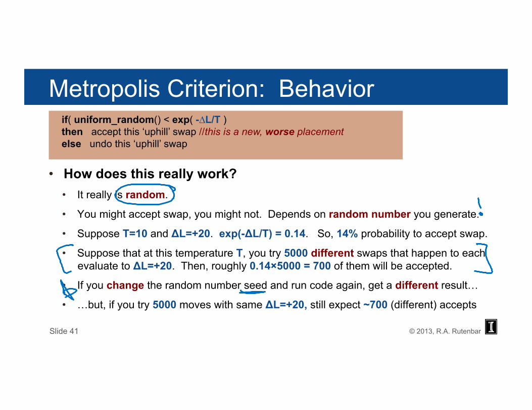
if( uniform_random() < exp( -∆L/T ) then accept this ‘uphill’ swap //this is a new, worse placement else undo this ‘uphill’ swap
Metropolis Criterion: Behavior
• How does this really work? • It really is random.
• You might accept swap, you might not. Depends on random number you generate.
• Suppose T=10 and ΔL=+20. exp(-ΔL/T) = 0.14. So, 14% probability to accept swap.
• Suppose that at this temperature T, you try 5000 different swaps that happen to each evaluate to ΔL=+20. Then, roughly 0.14×5000 = 700 of them will be accepted.
• If you change the random number seed and run code again, get a different result…
• …but, if you try 5000 moves with same ΔL=+20, still expect ~700 (different) accepts
Slide 41
© 2013, R.A. Rutenbar
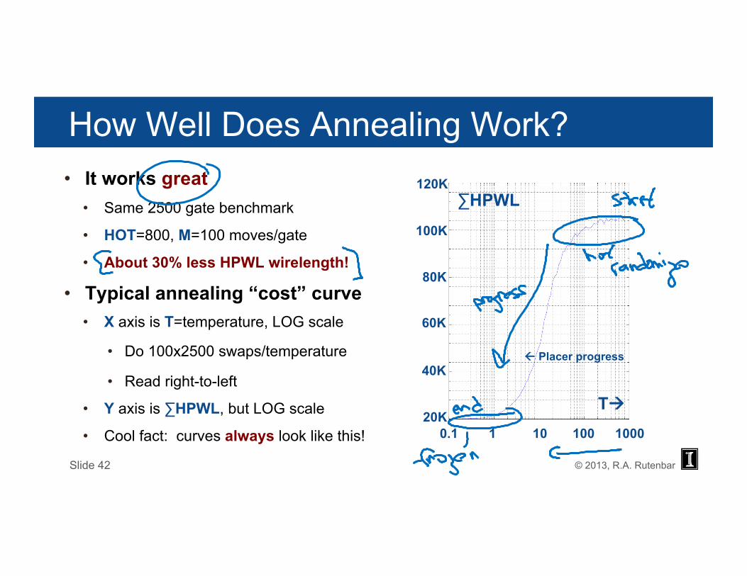
How Well Does Annealing Work? • It works great
• Same 2500 gate benchmark
• HOT=800, M=100 moves/gate
• About 30% less HPWL wirelength!
• Typical annealing “cost” curve • X axis is T=temperature, LOG scale
• Do 100x2500 swaps/temperature
• Read right-to-left
• Y axis is ∑HPWL, but LOG scale
• Cool fact: curves always look like this!
Slide 42
0.1 1 10 100 1000
40K
60K
80K
100K
∑HPWL 120K
20K Tà
ß Placer progress

© 2013, R.A. Rutenbar
Another View of Annealing Dynamics
Slide 43
• Annealing placer • ~6500 gates
• Map is “net congestion” • Picture at end of each temperature
• Compute the BBOX of each net
• We estimate a “routing congestion” number for each of these BBOX’s
• We add to each gate slot in grid, the “congestion” number for each net BBOX
• Simple model of wire “complexity”
• Red = BAD, Blue = GOOD
© 2013, R.A. Rutenbar
About Simulated Annealing, In General • Frequently Asked Questions (FAQs)
• Does annealing always find the perfect, best global optimum?
• NO. It is just good at avoiding a lot of local minimums
• Does annealing work on every type of optimization problem?
• NO. But it does work on many. But it is not always the most efficient option
• Is annealing always slow– doing all those many swaps over many temperatures?
• NO. Lots of engineering tricks to speed it up
• Do I have to set all the parameters – HOT, M swaps/gate – by trial and error?
• NO. There are fancy adaptive techniques to determine these automatically
• What happens if I run my annealer several different times (different random seeds)?
• You get a different (random!) answer each time. Yes, this feels strange…
Slide 44
© 2013, R.A. Rutenbar
Annealing for Placement: Summary • Simulated annealing is a very famous, successful method
• Much better than dumb random improvement
• Dominant method for placers in 1980s, 1990s
• And still today – used in lots of other VLSI CAD tasks. Important to understand!
• But… not how we really do placers today • Annealing works well for up to 100K – 500K gates
• Annealing too inefficient for things with 1M+ gates
• Need yet another new set of ideas…
Slide 45

VLSI CAD: Logic to Layout
Rob A. Rutenbar University of Illinois
Lecture 9.6 ASIC Placement: Analytical Placement: Quadratic Wirelength Model
© 2013, R.A. Rutenbar
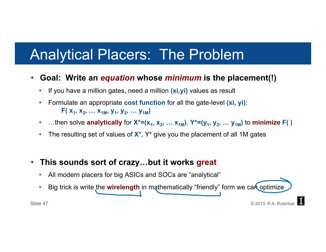
Analytical Placers: The Problem • Goal: Write an equation whose minimum is the placement(!)
• If you have a million gates, need a million (xi,yi) values as result
• Formulate an appropriate cost function for all the gate-level (xi, yi): F( x1, x2, … x1M, y1, y2, … y1M)
• …then solve analytically for X*=(x1, x2, … x1M), Y*=(y1, y2, … y1M) to minimize F( )
• The resulting set of values of X*, Y* give you the placement of all 1M gates
• This sounds sort of crazy…but it works great • All modern placers for big ASICs and SOCs are “analytical”
• Big trick is write the wirelength in mathematically “friendly” form we can optimize
Slide 47
© 2013, R.A. Rutenbar
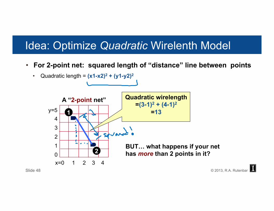
Idea: Optimize Quadratic Wirelenth Model • For 2-point net: squared length of “distance” line between points
• Quadratic length = (x1-x2)2 + (y1-y2)2
Slide 48
x=0 1 2 3 4
y=5 4 3 2 1 0
A “2-point net” Quadratic wirelength =(3-1)2 + (4-1)2
=13 1
2BUT… what happens if your net has more than 2 points in it?
© 2013, R.A. Rutenbar x=0 1 2 3 4
y=5 4 3 2 1 0
Clique model
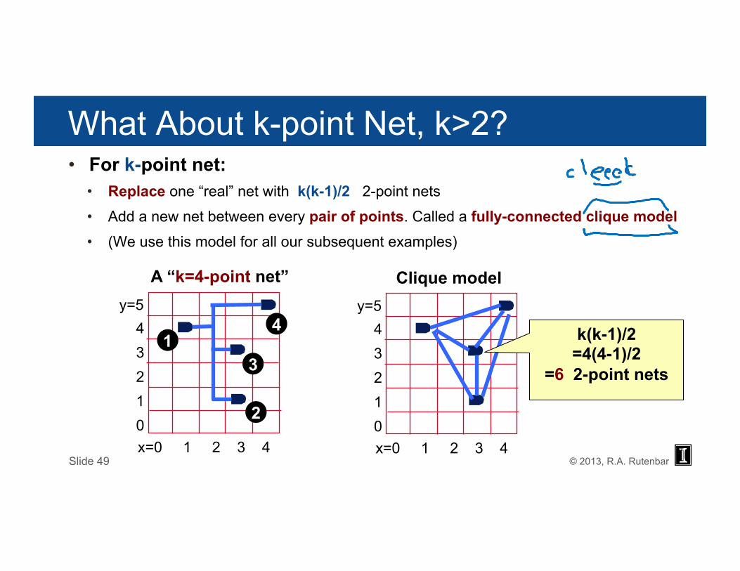
What About k-point Net, k>2? • For k-point net:
• Replace one “real” net with k(k-1)/2 2-point nets
• Add a new net between every pair of points. Called a fully-connected clique model • (We use this model for all our subsequent examples)
Slide 49 x=0 1 2 3 4
y=5 4 3 2 1 0
A “k=4-point net”
2
4 k(k-1)/2 =4(4-1)/2
=6 2-point nets
13
© 2013, R.A. Rutenbar
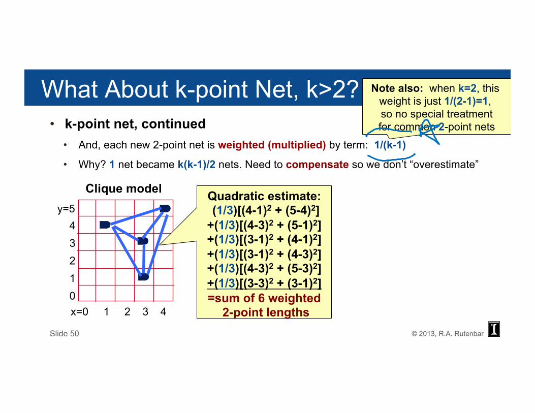
What About k-point Net, k>2? • k-point net, continued
• And, each new 2-point net is weighted (multiplied) by term: 1/(k-1)
• Why? 1 net became k(k-1)/2 nets. Need to compensate so we don’t “overestimate”
Slide 50
x=0 1 2 3 4
y=5 4 3 2 1 0
Clique model Quadratic estimate: (1/3)[(4-1)2 + (5-4)2] +(1/3)[(4-3)2 + (5-1)2] +(1/3)[(3-1)2 + (4-1)2] +(1/3)[(3-1)2 + (4-3)2] +(1/3)[(4-3)2 + (5-3)2] +(1/3)[(3-3)2 + (3-1)2] =sum of 6 weighted
2-point lengths
Note also: when k=2, this weight is just 1/(2-1)=1, so no special treatment for common 2-point nets
© 2013, R.A. Rutenbar
One More Big Idea: Gates as “Points” • To make the math work out easily, one more simplification:
• Ignore the physical size of all the gate – pretend gates are dimensionless points
• And, we will ignore (for now…) constraint that gates can’t go on top of each other
• Sounds strange. Why…? • Allows us to write a very simple, very elegant “equation” for the placement
• And, we can solve it, quickly and effectively
• And, we can then use another set of methods – later in this lecture – to repair this
Slide 51
© 2013, R.A. Rutenbar
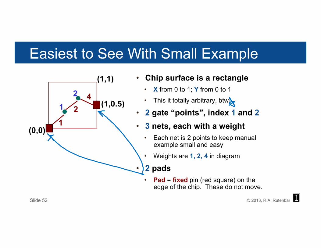
Easiest to See With Small Example • Chip surface is a rectangle
• X from 0 to 1; Y from 0 to 1
• This it totally arbitrary, btw
• 2 gate “points”, index 1 and 2 • 3 nets, each with a weight
• Each net is 2 points to keep manual example small and easy
• Weights are 1, 2, 4 in diagram
• 2 pads • Pad = fixed pin (red square) on the
edge of the chip. These do not move.
Slide 52
1 2
(0,0)
(1,0.5)
1 2
4
(1,1)
© 2013, R.A. Rutenbar
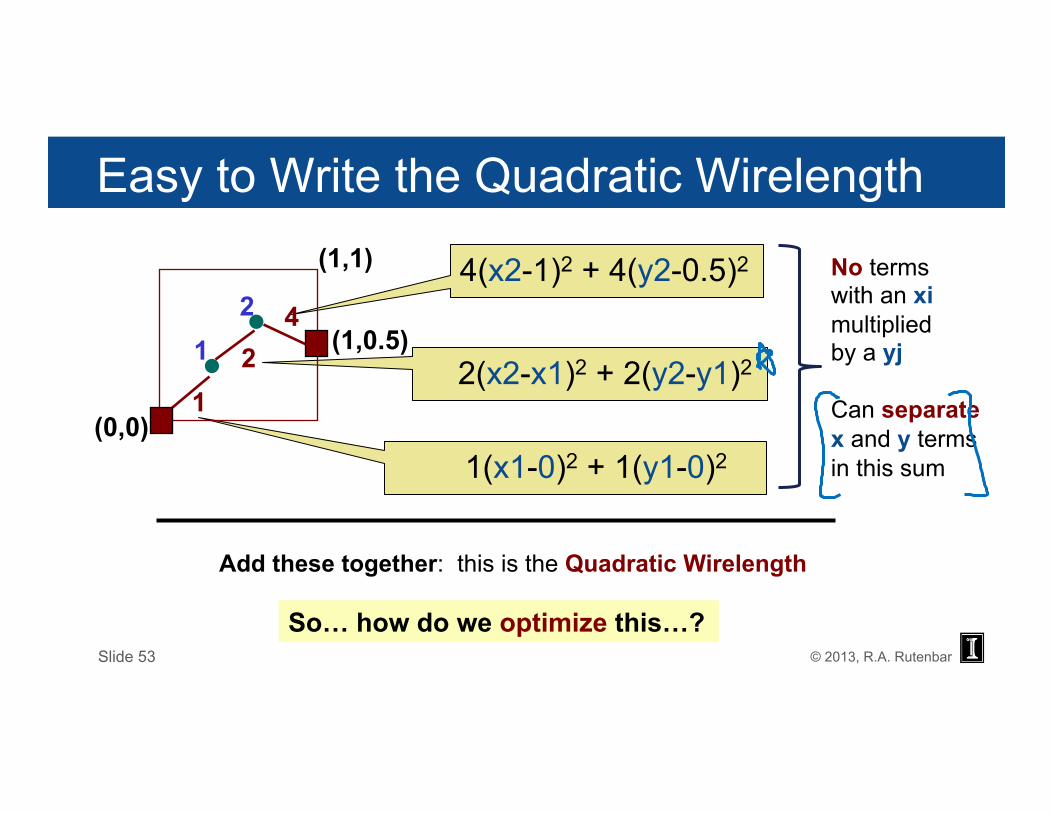
Easy to Write the Quadratic Wirelength
Slide 53
4(x2-1)2 + 4(y2-0.5)2
2(x2-x1)2 + 2(y2-y1)2
1(x1-0)2 + 1(y1-0)2
Add these together: this is the Quadratic Wirelength
1 2
(0,0)
(1,0.5)
1 2
4
(1,1)
So… how do we optimize this…?
No terms with an xi multiplied by a yj Can separate x and y terms in this sum

VLSI CAD: Logic to Layout
Rob A. Rutenbar University of Illinois
Lecture 9.7 ASIC Placement: Analytical Placement: Quadratic Placement
© 2013, R.A. Rutenbar
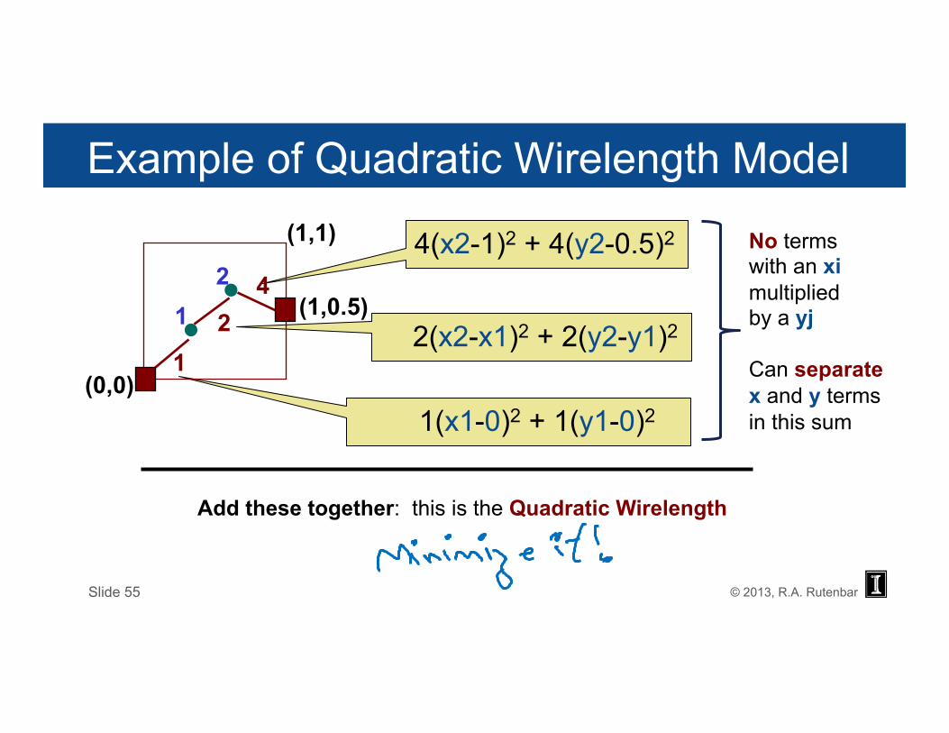
Example of Quadratic Wirelength Model
Slide 55
4(x2-1)2 + 4(y2-0.5)2
2(x2-x1)2 + 2(y2-y1)2
1(x1-0)2 + 1(y1-0)2
Add these together: this is the Quadratic Wirelength
1 2
(0,0)
(1,0.5)
1 2
4
(1,1) No terms with an xi multiplied by a yj Can separate x and y terms in this sum
© 2013, R.A. Rutenbar
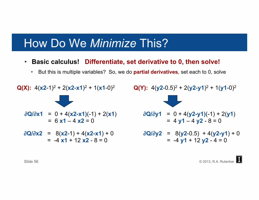
How Do We Minimize This? • Basic calculus! Differentiate, set derivative to 0, then solve!
• But this is multiple variables? So, we do partial derivatives, set each to 0, solve
Slide 56
Q(X): 4(x2-1)2 + 2(x2-x1)2 + 1(x1-0)2 Q(Y): 4(y2-0.5)2 + 2(y2-y1)2 + 1(y1-0)2
∂Q/∂x2 = 8(x2-1) + 4(x2-x1) + 0 = -4 x1 + 12 x2 - 8 = 0
∂Q/∂x1 = 0 + 4(x2-x1)(-1) + 2(x1) = 6 x1 – 4 x2 = 0
∂Q/∂y2 = 8(y2-0.5) + 4(y2-y1) + 0 = -4 y1 + 12 y2 - 4 = 0
∂Q/∂y1 = 0 + 4(y2-y1)(-1) + 2(y1) = 4 y1 – 4 y2 - 8 = 0
© 2013, R.A. Rutenbar
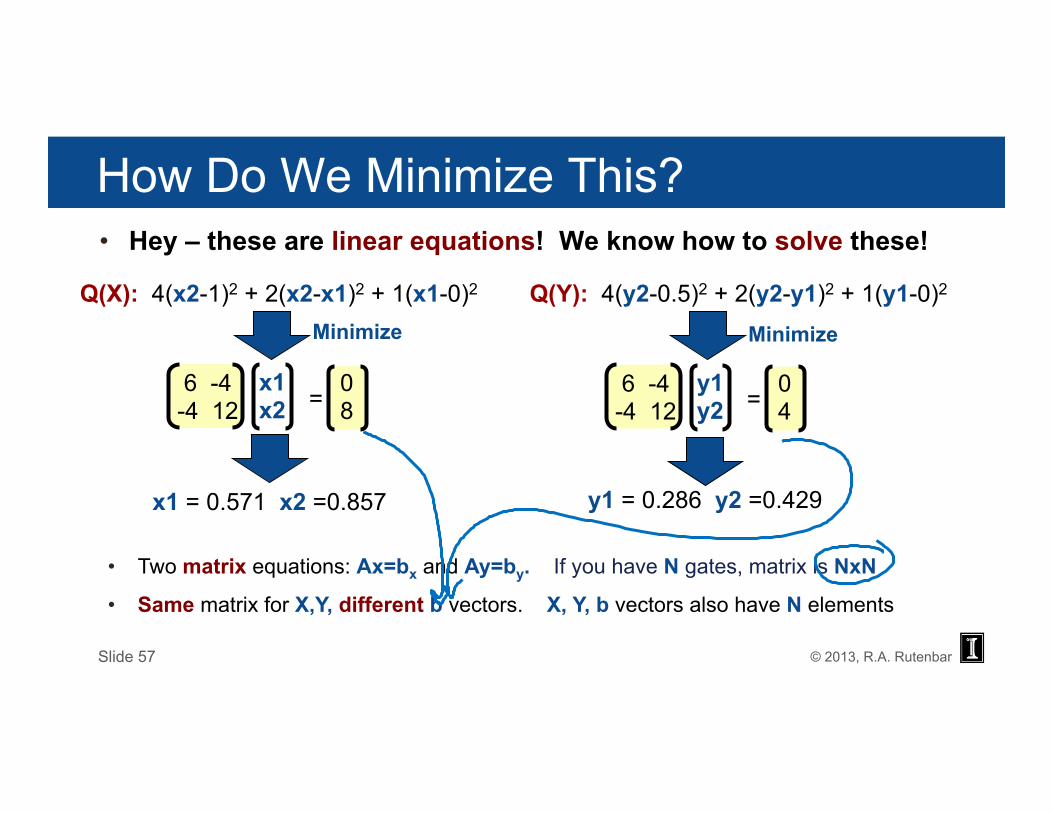
How Do We Minimize This? • Hey – these are linear equations! We know how to solve these!
Slide 57
Q(X): 4(x2-1)2 + 2(x2-x1)2 + 1(x1-0)2 Q(Y): 4(y2-0.5)2 + 2(y2-y1)2 + 1(y1-0)2
x1 = 0.571 x2 =0.857 y1 = 0.286 y2 =0.429
• Two matrix equations: Ax=bx and Ay=by. If you have N gates, matrix is NxN
• Same matrix for X,Y, different b vectors. X, Y, b vectors also have N elements
6 -4 -4 12
x1 x2 = 0
8 6 -4 -4 12
y1 y2 = 0
4
Minimize Minimize
© 2013, R.A. Rutenbar
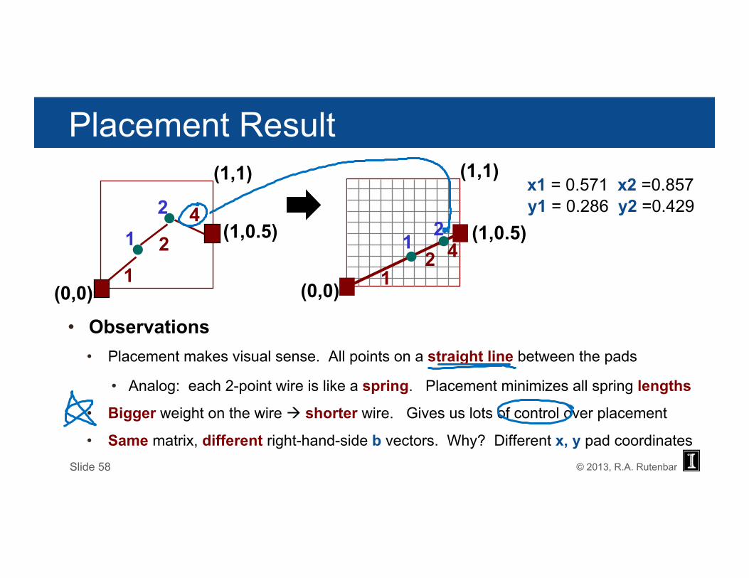
Placement Result
• Observations • Placement makes visual sense. All points on a straight line between the pads
• Analog: each 2-point wire is like a spring. Placement minimizes all spring lengths
• Bigger weight on the wire à shorter wire. Gives us lots of control over placement
• Same matrix, different right-hand-side b vectors. Why? Different x, y pad coordinates Slide 58
1 2
(0,0)
(1,0.5)
1 2
4
(1,1)
(0,0)
(1,0.5)
(1,1) x1 = 0.571 x2 =0.857 y1 = 0.286 y2 =0.429
1 2 4 2
1
© 2013, R.A. Rutenbar
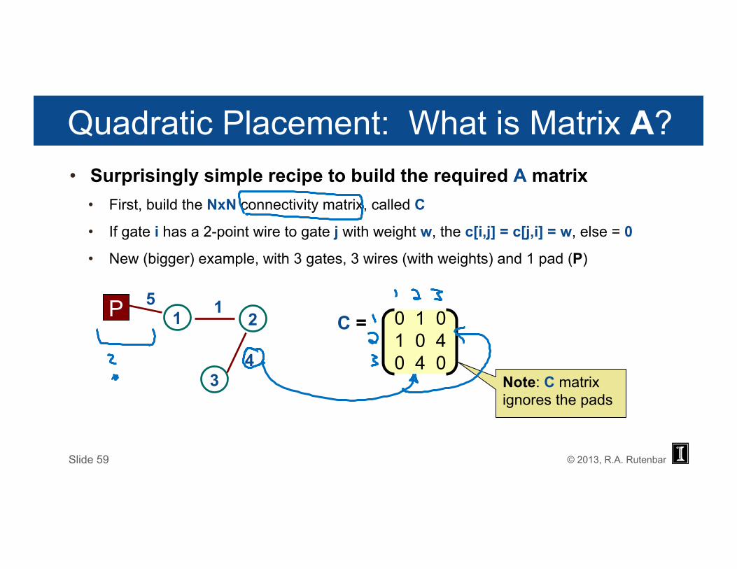
Quadratic Placement: What is Matrix A? • Surprisingly simple recipe to build the required A matrix
• First, build the NxN connectivity matrix, called C
• If gate i has a 2-point wire to gate j with weight w, the c[i,j] = c[j,i] = w, else = 0
• New (bigger) example, with 3 gates, 3 wires (with weights) and 1 pad (P)
Slide 59
1 2 1
3 4
C = 0 1 0 1 0 4 0 4 0
P 5
Note: C matrix ignores the pads
© 2013, R.A. Rutenbar
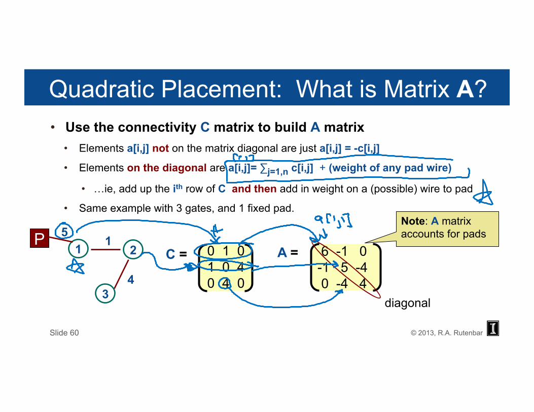
Quadratic Placement: What is Matrix A? • Use the connectivity C matrix to build A matrix
• Elements a[i,j] not on the matrix diagonal are just a[i,j] = -c[i,j]
• Elements on the diagonal are a[i,j]= ∑j=1,n c[i,j] + (weight of any pad wire)
• …ie, add up the ith row of C and then add in weight on a (possible) wire to pad
• Same example with 3 gates, and 1 fixed pad.
Slide 60
C = 1 2 1
3 4
0 1 0 1 0 4 0 4 0
A = 6 -1 0 -1 5 -4 0 -4 4
P 5
diagonal
Note: A matrix accounts for pads
© 2013, R.A. Rutenbar
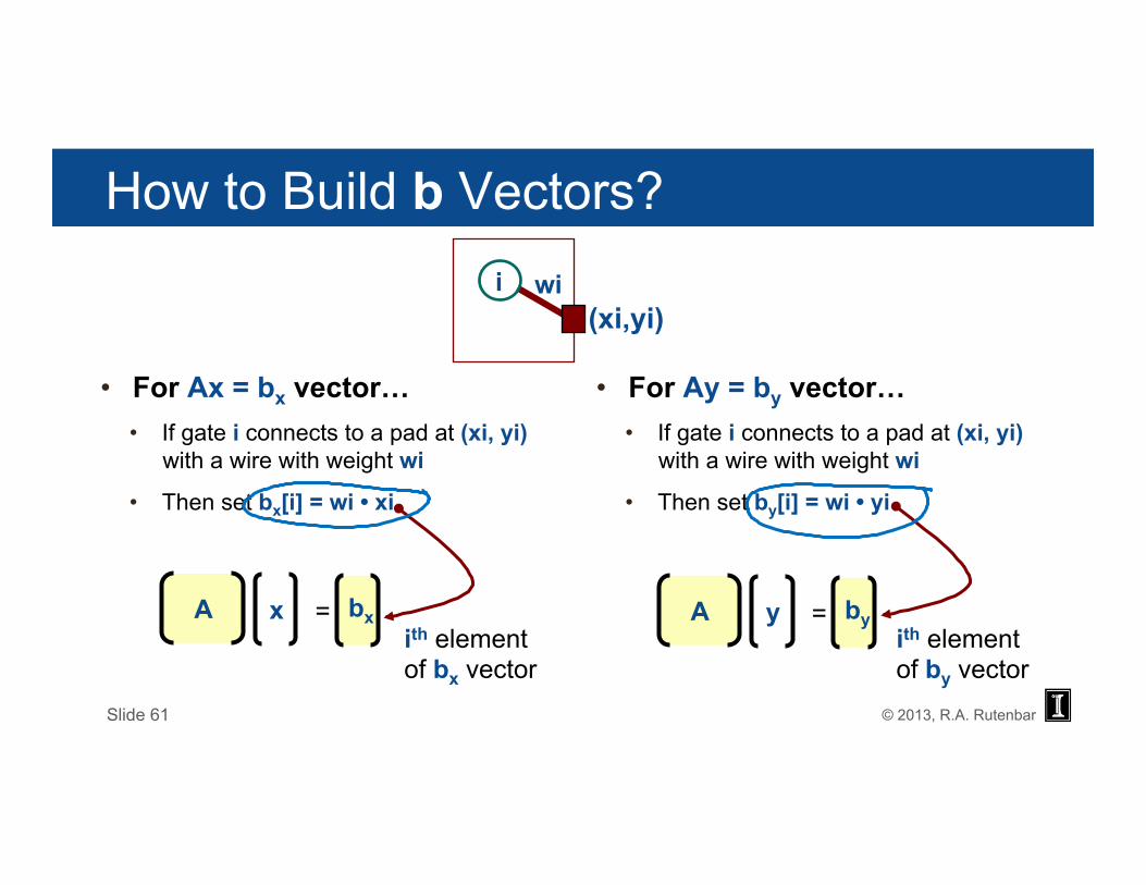
How to Build b Vectors?
• For Ax = bx vector… • If gate i connects to a pad at (xi, yi)
with a wire with weight wi
• Then set bx[i] = wi • xi
• For Ay = by vector… • If gate i connects to a pad at (xi, yi)
with a wire with weight wi
• Then set by[i] = wi • yi
Slide 61
(xi,yi) i
A x = bx ith element of bx vector
ith element of by vector
A y = by
wi
© 2013, R.A. Rutenbar
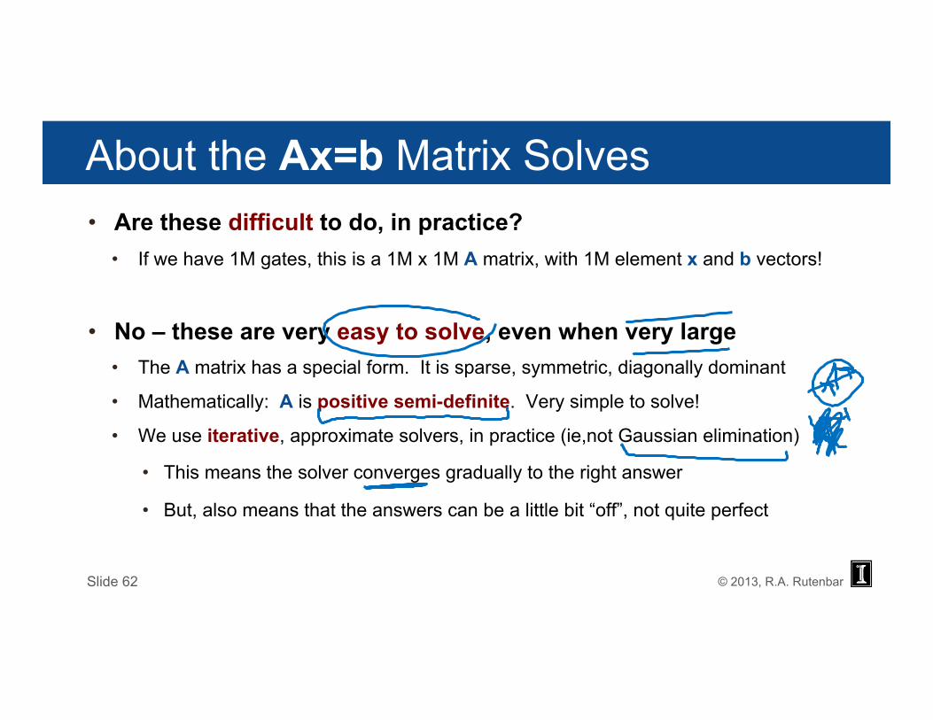
About the Ax=b Matrix Solves • Are these difficult to do, in practice?
• If we have 1M gates, this is a 1M x 1M A matrix, with 1M element x and b vectors!
• No – these are very easy to solve, even when very large • The A matrix has a special form. It is sparse, symmetric, diagonally dominant
• Mathematically: A is positive semi-definite. Very simple to solve!
• We use iterative, approximate solvers, in practice (ie,not Gaussian elimination)
• This means the solver converges gradually to the right answer
• But, also means that the answers can be a little bit “off”, not quite perfect
Slide 62
© 2013, R.A. Rutenbar
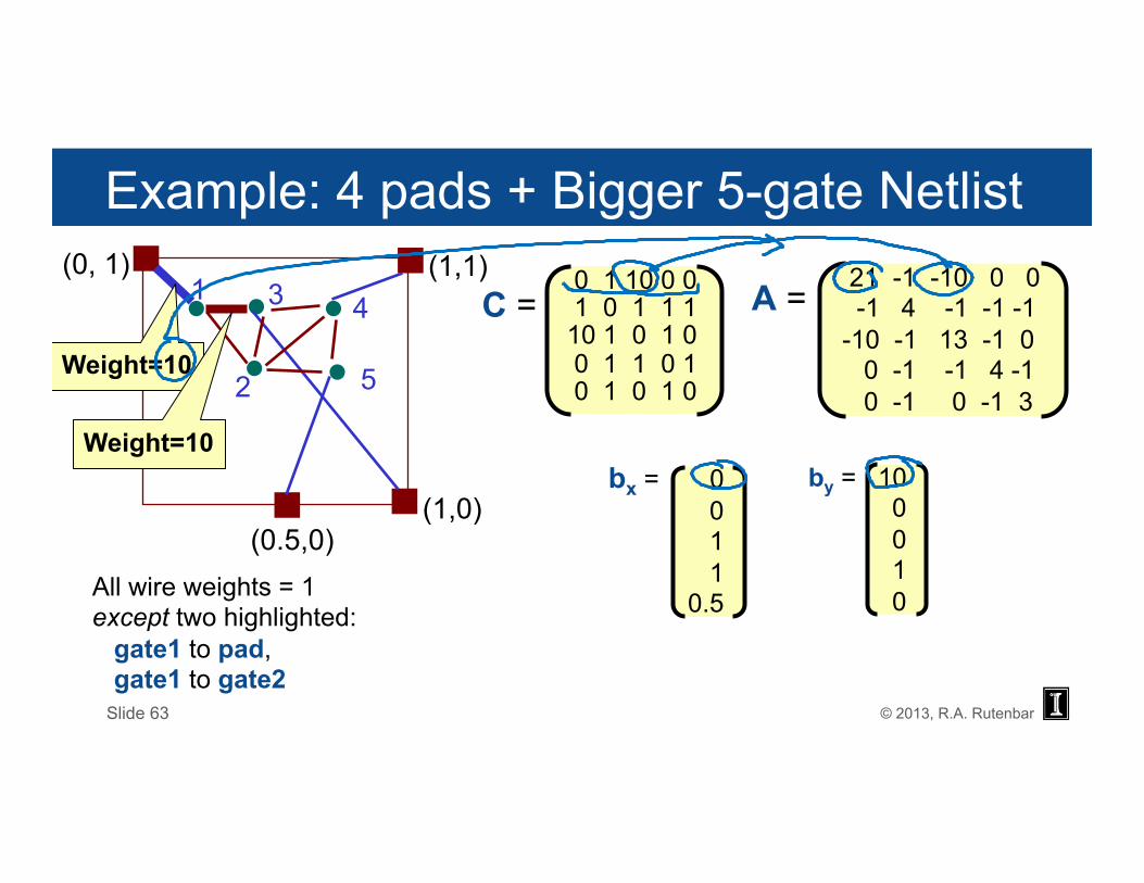
Example: 4 pads + Bigger 5-gate Netlist
1
2
3 4
(1,0)
(0, 1)
(0.5,0)
5
(1,1) C =
0 1 10 0 0 1 0 1 1 1 10 1 0 1 0 0 1 1 0 1 0 1 0 1 0
All wire weights = 1 except two highlighted: gate1 to pad, gate1 to gate2
Weight=10
Weight=10
A = 21 -1 -10 0 0 -1 4 -1 -1 -1 -10 -1 13 -1 0 0 -1 -1 4 -1 0 -1 0 -1 3
bx = 0 0 1 1 0.5
by = 10 0 0 1 0
Slide 63
© 2013, R.A. Rutenbar
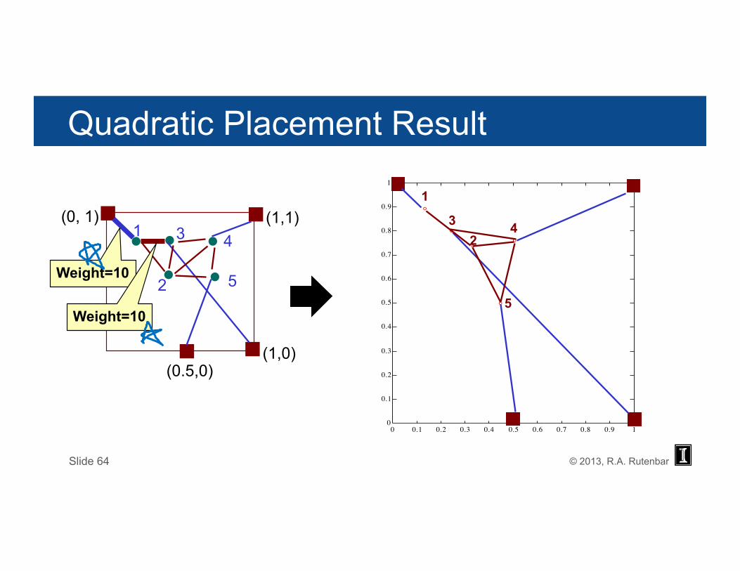
Quadratic Placement Result
1
2
3 4
(1,0)
(0, 1)
(0.5,0)
5
(1,1)
Weight=10
Weight=10
0
0.1
0.2
0.3
0.4
0.5
0.6
0.7
0.8
0.9
1
0 0.1 0.2 0.3 0.4 0.5 0.6 0.7 0.8 0.9 1
1
5
4 3 2
Slide 64

VLSI CAD: Logic to Layout
Rob A. Rutenbar University of Illinois
Lecture 9.8 ASIC Placement: Analytical Placement: Recursive Partitioning
© 2013, R.A. Rutenbar
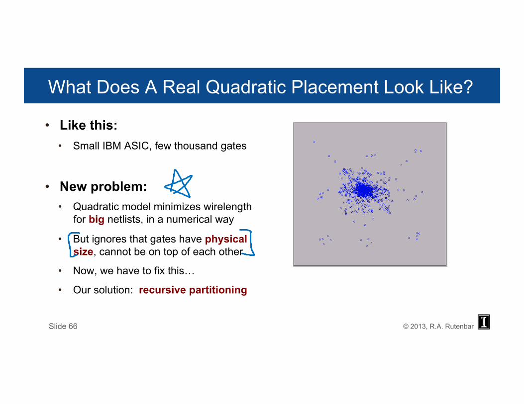
What Does A Real Quadratic Placement Look Like?
• Like this: • Small IBM ASIC, few thousand gates
• New problem: • Quadratic model minimizes wirelength
for big netlists, in a numerical way
• But ignores that gates have physical size, cannot be on top of each other
• Now, we have to fix this…
• Our solution: recursive partitioning
Slide 66
© 2013, R.A. Rutenbar
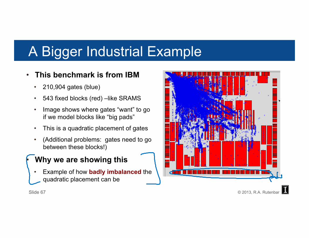
A Bigger Industrial Example • This benchmark is from IBM
• 210,904 gates (blue)
• 543 fixed blocks (red) –like SRAMS
• Image shows where gates “want” to go if we model blocks like “big pads”
• This is a quadratic placement of gates
• (Additional problems: gates need to go between these blocks!)
• Why we are showing this • Example of how badly imbalanced the
quadratic placement can be
Slide 67
© 2013, R.A. Rutenbar
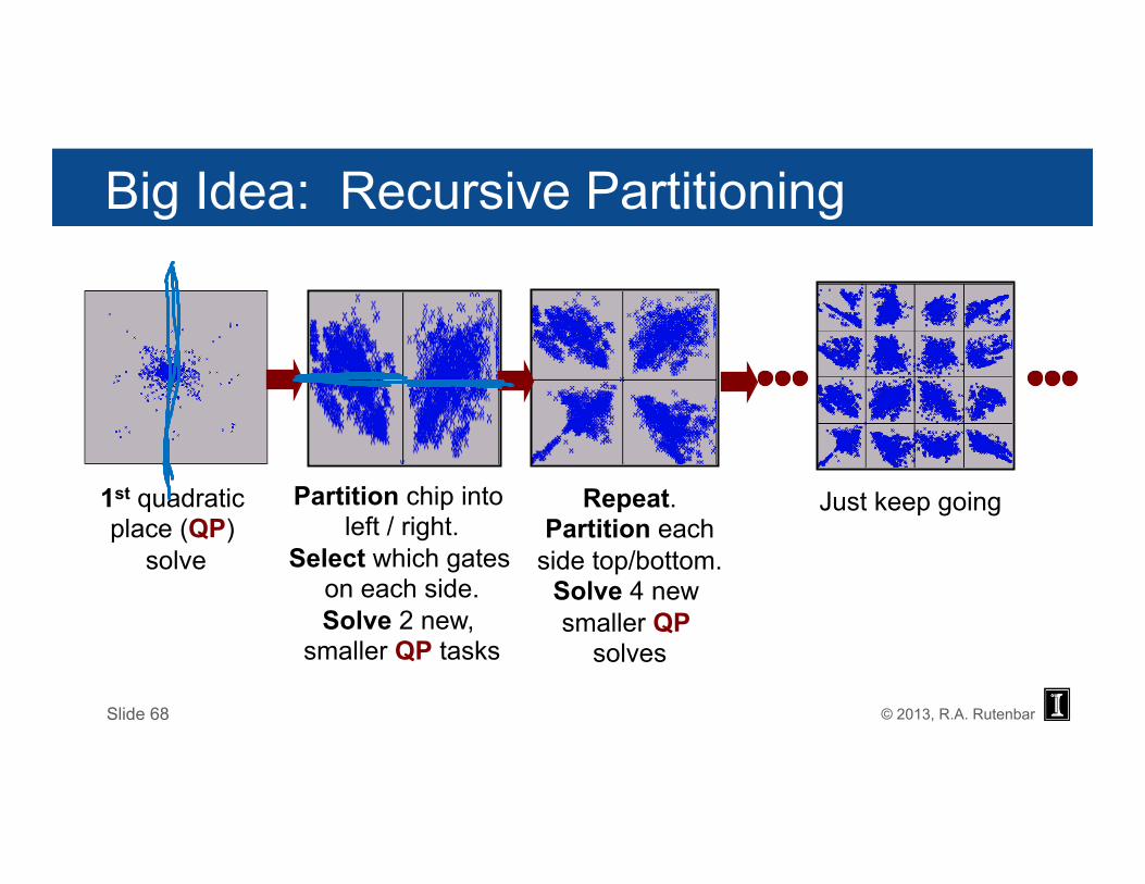
Big Idea: Recursive Partitioning
1st quadratic place (QP)
solve
Just keep going Partition chip into left / right.
Select which gates on each side. Solve 2 new,
smaller QP tasks
Repeat. Partition each
side top/bottom. Solve 4 new smaller QP
solves
Slide 68
© 2013, R.A. Rutenbar
Recursive Partitioning: Basic Steps • Partition
• How do we divide the chip into new, smaller placement tasks?
• Assignment • Which gates should go into each new, smaller region?
• Containment • Formulate new QP matrix solves so gates stay in new regions, with short wirelength
• Discuss one early strategy from a classical paper • Ren Song Tsay, Ernest Kuh, Chi Ping Hsu, “PROUD: A Sea-Of-gates Placement
Algorithm,” IEEE Design & Test of Computers, Dec 1988.
Slide 69
© 2013, R.A. Rutenbar
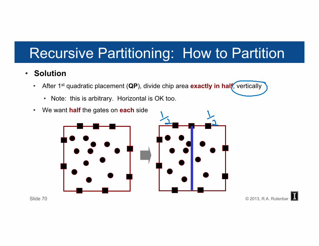
Recursive Partitioning: How to Partition • Solution
• After 1st quadratic placement (QP), divide chip area exactly in half, vertically
• Note: this is arbitrary. Horizontal is OK too.
• We want half the gates on each side
Slide 70
© 2013, R.A. Rutenbar
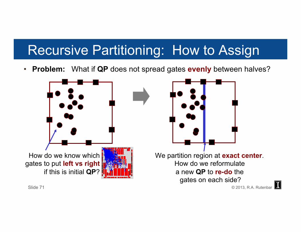
Recursive Partitioning: How to Assign • Problem: What if QP does not spread gates evenly between halves?
How do we know which gates to put left vs right
if this is initial QP?
We partition region at exact center. How do we reformulate a new QP to re-do the gates on each side?
Slide 71
© 2013, R.A. Rutenbar
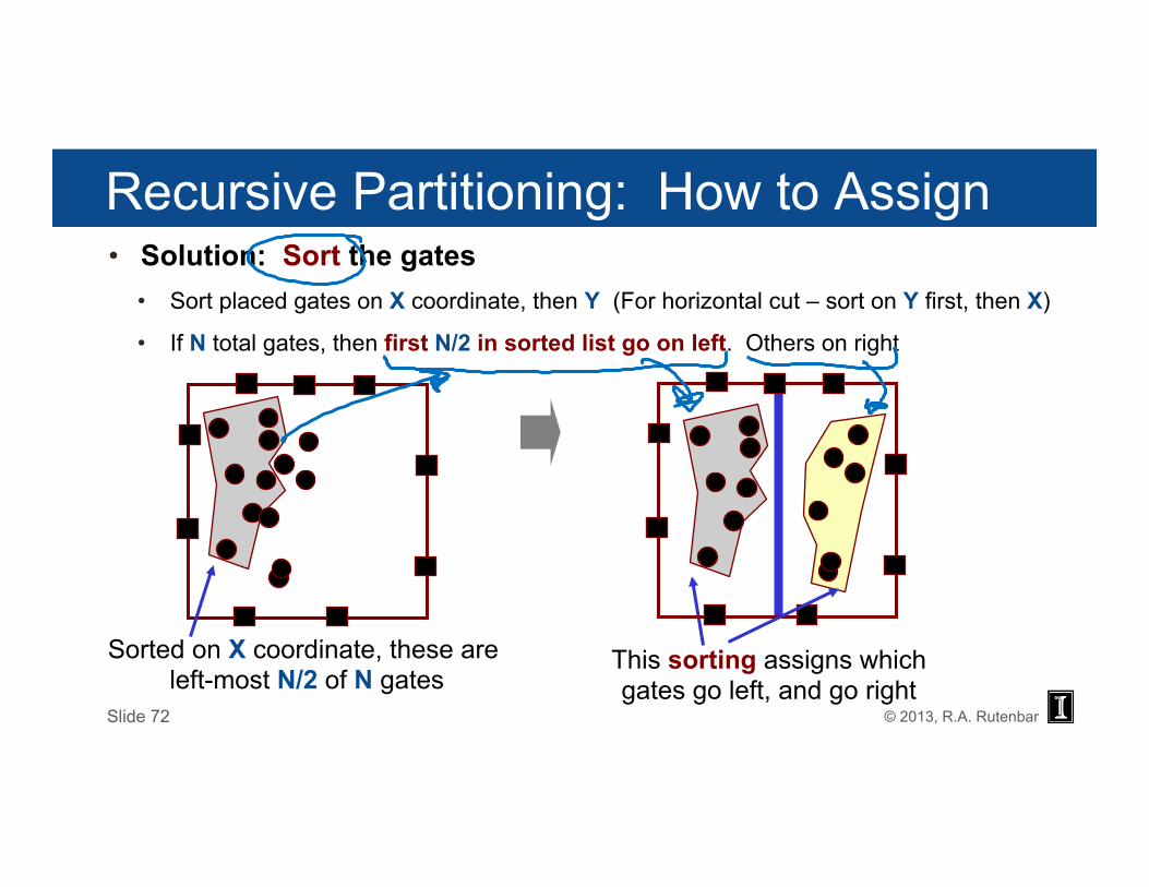
Recursive Partitioning: How to Assign • Solution: Sort the gates
• Sort placed gates on X coordinate, then Y (For horizontal cut – sort on Y first, then X)
• If N total gates, then first N/2 in sorted list go on left. Others on right
Sorted on X coordinate, these are left-most N/2 of N gates
This sorting assigns which gates go left, and go right
Slide 72
© 2013, R.A. Rutenbar
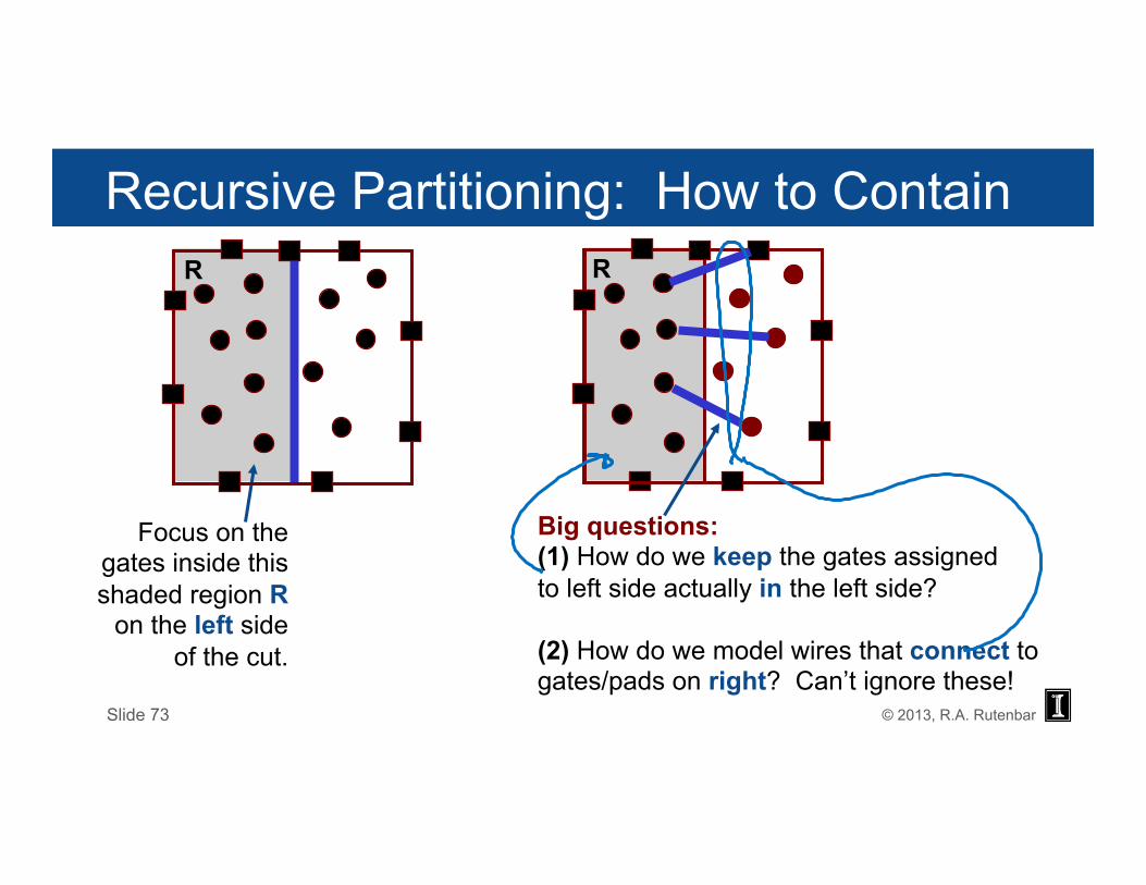
Recursive Partitioning: How to Contain
Focus on the gates inside this shaded region R
on the left side of the cut.
Slide 73
R
Big questions: (1) How do we keep the gates assigned to left side actually in the left side? (2) How do we model wires that connect to gates/pads on right? Can’t ignore these!
R
© 2013, R.A. Rutenbar
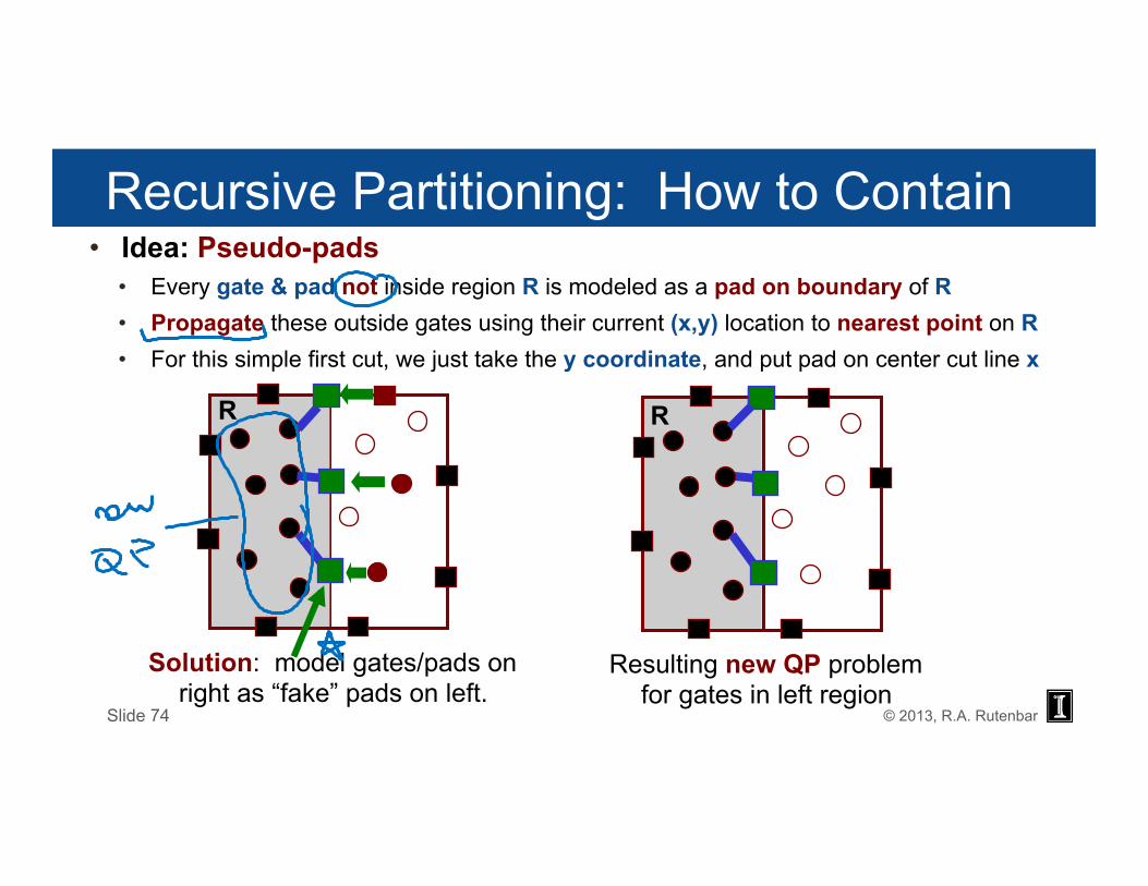
Recursive Partitioning: How to Contain • Idea: Pseudo-pads
• Every gate & pad not inside region R is modeled as a pad on boundary of R • Propagate these outside gates using their current (x,y) location to nearest point on R • For this simple first cut, we just take the y coordinate, and put pad on center cut line x
Solution: model gates/pads on right as “fake” pads on left.
Slide 74
R
Resulting new QP problem for gates in left region
R
© 2013, R.A. Rutenbar
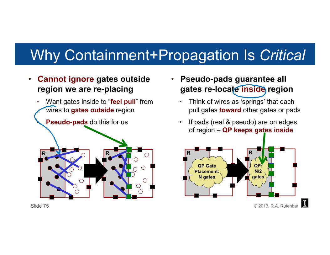
Why Containment+Propagation Is Critical • Cannot ignore gates outside
region we are re-placing • Want gates inside to “feel pull” from
wires to gates outside region
• Pseudo-pads do this for us
• Pseudo-pads guarantee all gates re-locate inside region • Think of wires as ‘springs’ that each
pull gates toward other gates or pads
• If pads (real & pseudo) are on edges of region – QP keeps gates inside
Slide 75
R R R R
QP Gate Placement:
N gates
QP: N/2
gates
VLSI CAD: Logic to Layout
Rob A. Rutenbar University of Illinois
Lecture 9.9 ASIC Placement: Analytical Placement: Recursive Partitioning Example
© 2013, R.A. Rutenbar
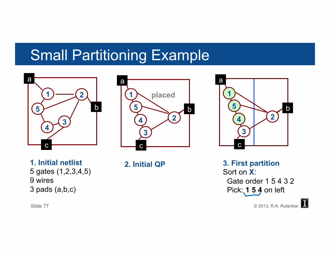
Small Partitioning Example
Slide 77
1 2
3
a
b
c
4
5
1. Initial netlist5 gates (1,2,3,4,5) 9 wires 3 pads (a,b,c)
a
b
c
2. Initial QP
2
3
1 5
4
placed
a
b
c
3. First partitionSort on X: Gate order 1 5 4 3 2 Pick: 1 5 4 on left
2
3
1 5
4
© 2013, R.A. Rutenbar
Small Partitioning Example
Slide 78
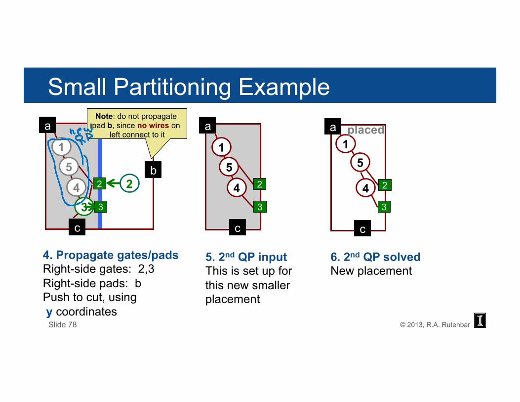
4. Propagate gates/pads Right-side gates: 2,3 Right-side pads: b Push to cut, using y coordinates
a
b
c
2
3
1 5
4 2
3
5. 2nd QP input This is set up for this new smaller placement
a
c
1 5
4 2
3
6. 2nd QP solved New placement
a
c
1 5
2
placed
3
4
Note: do not propagate pad b, since no wires on
left connect to it
© 2013, R.A. Rutenbar
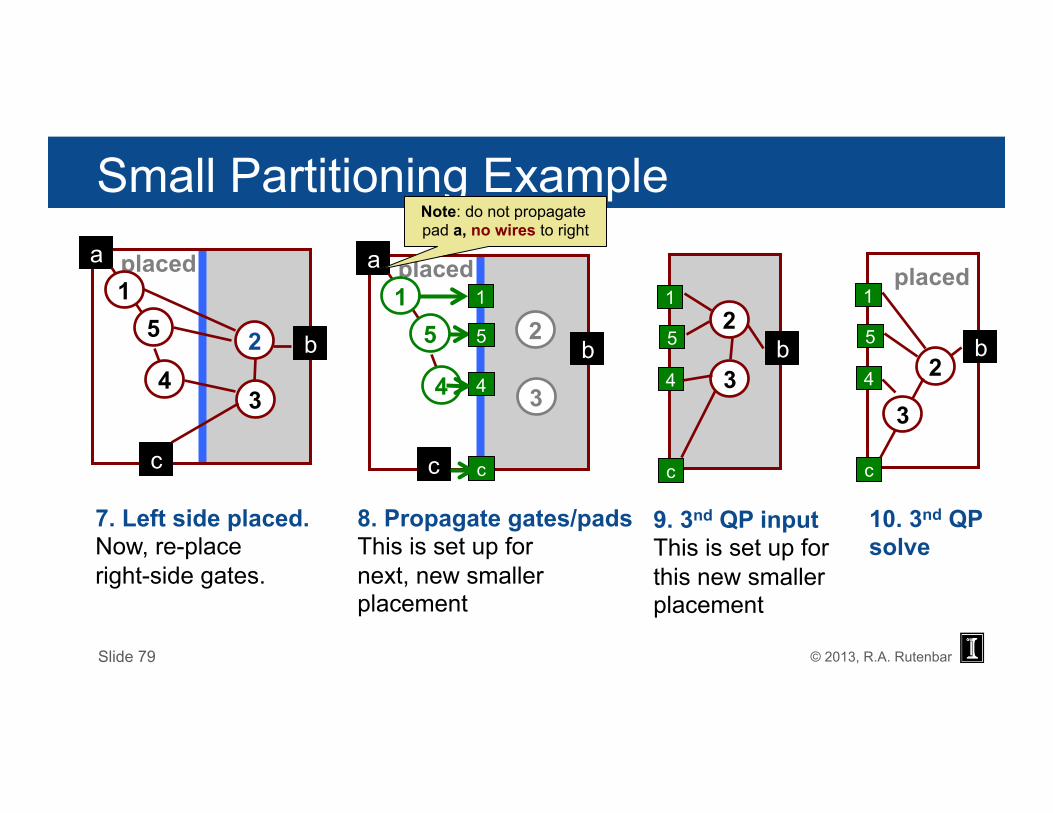
8. Propagate gates/pads This is set up for next, new smaller placement
a
b
c
2
placed
c
4
5
3
1 5
4
1
Small Partitioning Example
Slide 79
7. Left side placed. Now, re-place right-side gates.
a
b
c
2
3
placed 1
5
4
9. 3nd QP input This is set up for this new smaller placement
2 b
c
4
5
1
3 b
c
4
5
1
10. 3nd QP solve
placed
2
3
Note: do not propagate pad a, no wires to right
© 2013, R.A. Rutenbar
Small Partitioning Example
Slide 80
a
c
placed
b
placed
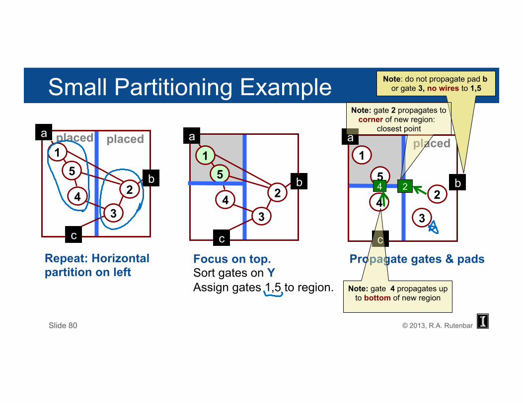
Repeat: Horizontal partition on left
2
3
1 5
4
Focus on top. Sort gates on Y Assign gates 1,5 to region.
a
c
b 2
3
1 5
4
a
c
3
1
5
4 b
placed
2 4 2
Propagate gates & pads
Note: do not propagate pad b or gate 3, no wires to 1,5
Note: gate 2 propagates to corner of new region:
closest point
Note: gate 4 propagates up to bottom of new region
© 2013, R.A. Rutenbar
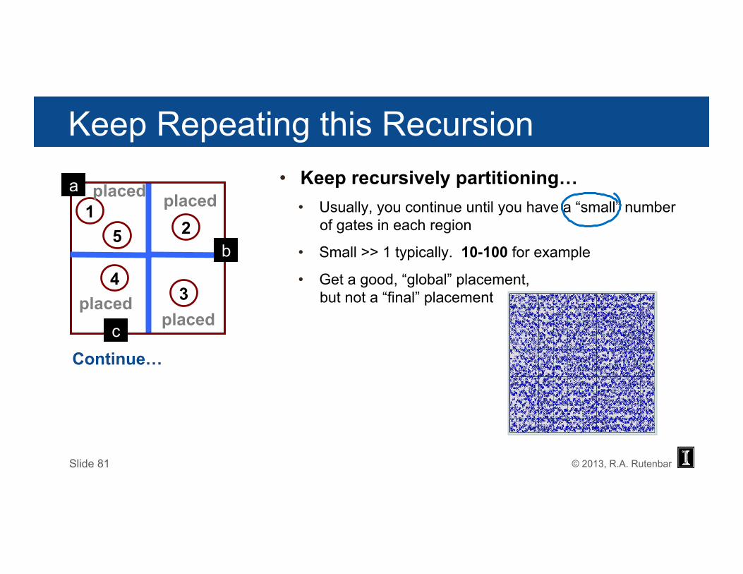
Keep Repeating this Recursion • Keep recursively partitioning…
• Usually, you continue until you have a “small” number of gates in each region
• Small >> 1 typically. 10-100 for example
• Get a good, “global” placement, but not a “final” placement
Slide 81
a
c
3
1 5
4 b
placed
2
Continue…
placed
placed
placed
© 2013, R.A. Rutenbar
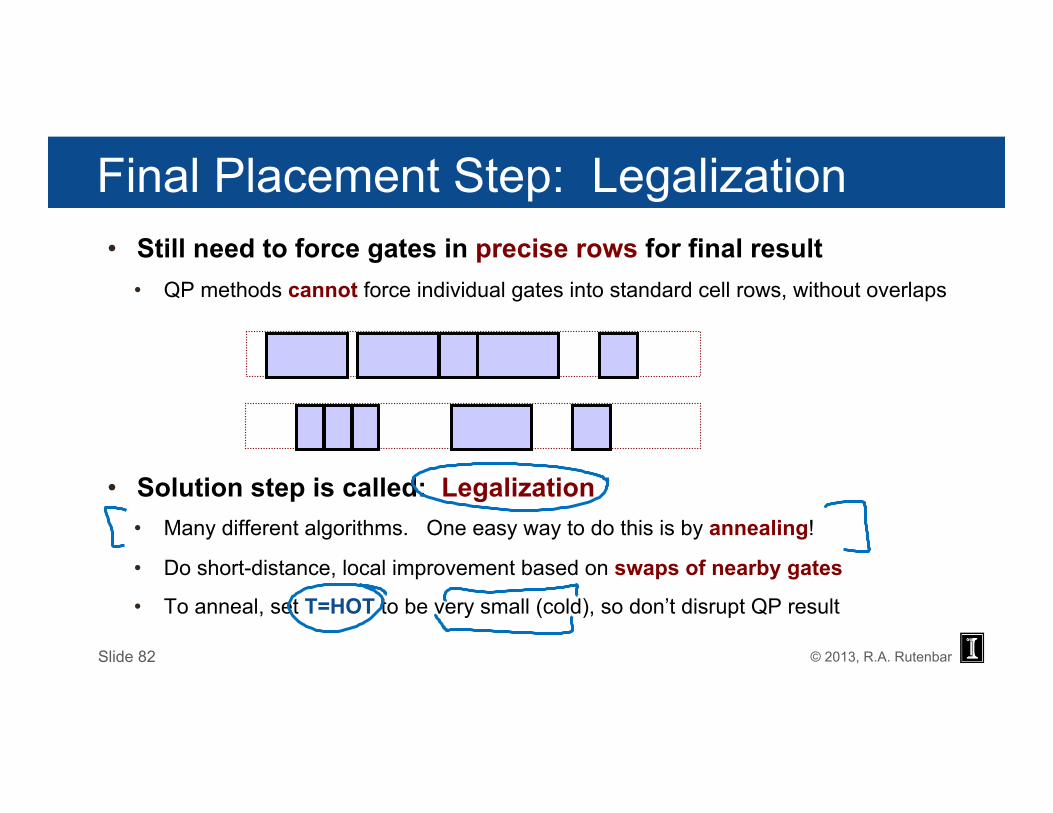
Final Placement Step: Legalization • Still need to force gates in precise rows for final result
• QP methods cannot force individual gates into standard cell rows, without overlaps
• Solution step is called: Legalization • Many different algorithms. One easy way to do this is by annealing!
• Do short-distance, local improvement based on swaps of nearby gates
• To anneal, set T=HOT to be very small (cold), so don’t disrupt QP result
Slide 82
© 2013, R.A. Rutenbar
Placement Summary • Early placers based on iterative improvement
• Simulated annealing is a very good, famous example
• Annealing stuff used widely in VLSI CAD – but not for placers. Too inefficient
• Modern placers are all analytical • Many different mathematical formulations, but all similar
• Numerically optimize a mathematically friendly model of wirelength
• Many modern placers can do some “legalization” at same time as wirelength!
• Quadratic placement is a famous, important, practical example
Slide 83