80GHz Notch Filter Design - people9 80GHz Notch Filter Design Figure 3 3D Notch filter HFSS...
24
DIGITAL PRODUCTIVITY FLAGSHIP 80GHz Notch Filter Design Mark De Alwis 10 June 2015
Transcript of 80GHz Notch Filter Design - people9 80GHz Notch Filter Design Figure 3 3D Notch filter HFSS...
DIGITAL PRODUCTIVITY FLAGSHIP
80GHz Notch Filter Design
Mark De Alwis
10 June 2015

ii 80GHz Notch Filter Design
iii 80GHz Notch Filter Design
Important disclaimer
CSIRO advises that the information contained in this publication comprises general statements based on
scientific research. The reader is advised and needs to be aware that such information may be incomplete
or unable to be used in any specific situation. No reliance or actions must therefore be made on that
information without seeking prior expert professional, scientific and technical advice. To the extent
permitted by law, CSIRO (including its employees and consultants) excludes all liability to any person for
any consequences, including but not limited to all losses, damages, costs, expenses and any other
compensation, arising directly or indirectly from using this publication (in part or in whole) and any
information or material contained in it.
4 80GHz Notch Filter Design
Contents
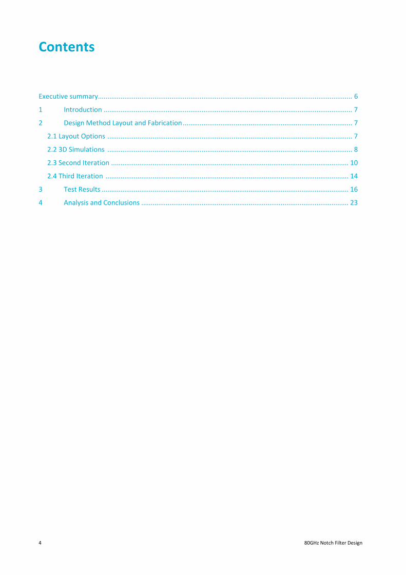
Executive summary....................................................................................................................................... 6
1 Introduction .................................................................................................................................... 7
2 Design Method Layout and Fabrication .......................................................................................... 7
2.1 Layout Options .................................................................................................................................. 7
2.2 3D Simulations .................................................................................................................................. 8
2.3 Second Iteration .............................................................................................................................. 10
2.4 Third Iteration ................................................................................................................................. 14
3 Test Results ................................................................................................................................... 16
4 Analysis and Conclusions .............................................................................................................. 23
5 80GHz Notch Filter Design
Figures
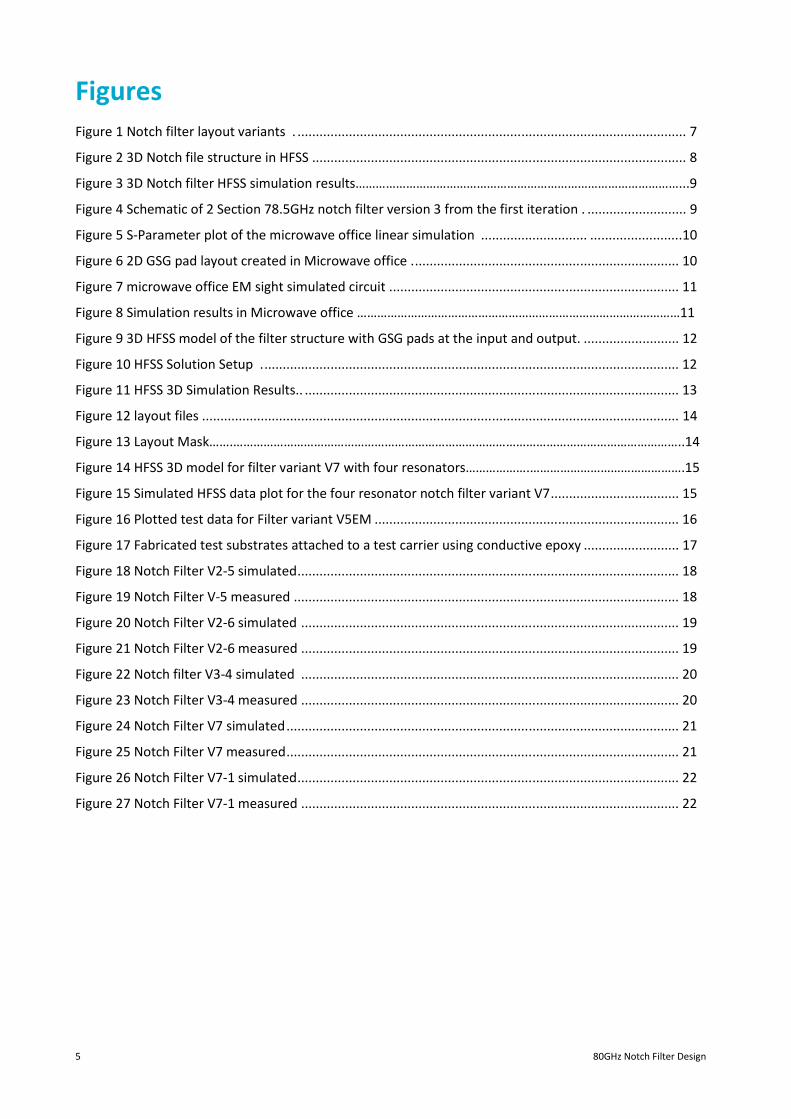
Figure 1 Notch filter layout variants . .......................................................................................................... 7
Figure 2 3D Notch file structure in HFSS . ..................................................................................................... 8
Figure 3 3D Notch filter HFSS simulation results……………………………………………………………………………………...9
Figure 4 Schematic of 2 Section 78.5GHz notch filter version 3 from the first iteration . ........................... 9
Figure 5 S-Parameter plot of the microwave office linear simulation ............................. .........................10
Figure 6 2D GSG pad layout created in Microwave office . ........................................................................ 10
Figure 7 microwave office EM sight simulated circuit . .............................................................................. 11
Figure 8 Simulation results in Microwave office ……………………………………………………………………………………11
Figure 9 3D HFSS model of the filter structure with GSG pads at the input and output. .......................... 12
Figure 10 HFSS Solution Setup . ................................................................................................................. 12
Figure 11 HFSS 3D Simulation Results.. ...................................................................................................... 13
Figure 12 layout files .................................................................................................................................. 14
Figure 13 Layout Mask…….……………………………………………………………………………………………………………………..14
Figure 14 HFSS 3D model for filter variant V7 with four resonators……………….……………………………………….15
Figure 15 Simulated HFSS data plot for the four resonator notch filter variant V7 ................................... 15
Figure 16 Plotted test data for Filter variant V5EM ................................................................................... 16
Figure 17 Fabricated test substrates attached to a test carrier using conductive epoxy .......................... 17
Figure 18 Notch Filter V2-5 simulated ........................................................................................................ 18
Figure 19 Notch Filter V-5 measured ......................................................................................................... 18
Figure 20 Notch Filter V2-6 simulated ....................................................................................................... 19
Figure 21 Notch Filter V2-6 measured ....................................................................................................... 19
Figure 22 Notch filter V3-4 simulated ....................................................................................................... 20
Figure 23 Notch Filter V3-4 measured ....................................................................................................... 20
Figure 24 Notch Filter V7 simulated ........................................................................................................... 21
Figure 25 Notch Filter V7 measured ........................................................................................................... 21
Figure 26 Notch Filter V7-1 simulated ........................................................................................................ 22
Figure 27 Notch Filter V7-1 measured ....................................................................................................... 22
6 80GHz Notch Filter Design
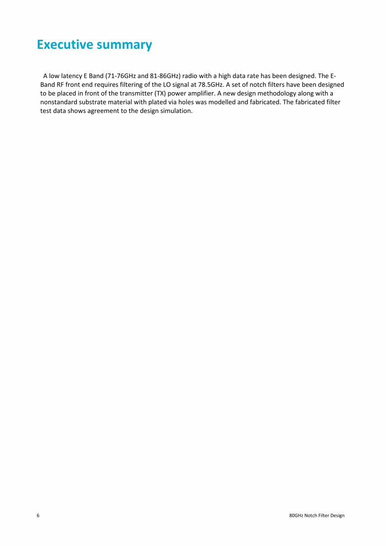
Executive summary
A low latency E Band (71-76GHz and 81-86GHz) radio with a high data rate has been designed. The E-
Band RF front end requires filtering of the LO signal at 78.5GHz. A set of notch filters have been designed
to be placed in front of the transmitter (TX) power amplifier. A new design methodology along with a
nonstandard substrate material with plated via holes was modelled and fabricated. The fabricated filter
test data shows agreement to the design simulation.

7 80GHz Notch Filter Design
1 Introduction
The LO signal is a CW signal entering a sub harmonic mixer. The mixer doubles the LO signal frequency to
78.5GHz prior to performing an up conversion for the transmitter. Additional filtering is required at the
front end since the LO signal is in band to the TX power amplifier. The most suitable filter type for this task
is a notch filter. Initial design considerations required a high precision sputtered gold etch back process for
fabrication of the filters. Traditionally the substrate material of choice used for this process is ceramic
Alumina. However, the dielectric constant of Alumina is too high (9.7 @ 10GHz) to realize the thin film
circuit required. Therefore, Quartz was selected for its lower dielectric constant of 3.826. A substrate
thickness of 4mil was chosen to minimize the step from the GaAs Amplifier chip and the waveguide feed
substrate.
Three iterations were required to perfect the design method. In the initial run the substrates were
modelled and fabricated with no ground signal ground (GSG) probable input and output pads. This required
the test substrates to be wire bonded to 50 Ohm RF input and output lines with GSG pads. The results were
not satisfactory since the additional circuitry added unwanted parasitics which distorted the results.
The next iteration added input and output GSG pads into the simulated models and resulting fabricated
substrates. However, the full 3-D simulation carried out in HFSS had an error which uniformly shifted the
notch frequency of all the fabricated variants up in frequency by 2GHz to 3GHz. A third iteration was
carried out correcting the error in HFSS to yield good results.
2. Design Method Layout and Fabrication
2.1 Layout Options Notch filters are formed by introducing coupled RF lines adjacent to the main transmission line carrying the
RF signal. The number of coupled lines determines the depth of the notch. The notch frequency is
determined by the length of the coupled section of RF line. The coupled line needs to be terminated at one
end with an open stub. The length of the open stub and the length of the coupled line segment are
between λ/4 and λ/8 where λ= wave length of the RF frequency of the notch. The open stub tends to be
closer to λ/4 while the coupled line length tends to be closer to λ/8. If more than one coupled line segment
is used the distance between coupled line segments is also critical to the simulation. The width of the main
RF transmission line is maintained at 50 Ohm impedance width. The width of the coupled line segments are
usually held to one uniform value determined by simulation and optimization. Applying simulation and
optimization methods described next four layout variants shown in figure 1 were designed. The radial open
stub (in V3EM & V3LN) was used to obtain a slightly wider notch. Two coupled line segments were chosen
due to the available space and the target specification of -15dB rejection.
Figure 1 Notch filter layout variants
8 80GHz Notch Filter Design
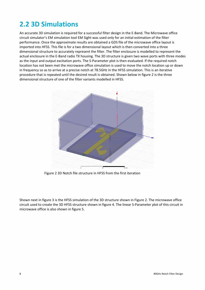
2.2 3D Simulations An accurate 3D simulation is required for a successful filter design in the E-Band. The Microwave office
circuit simulator’s EM simulation tool EM Sight was used only for an initial estimation of the filter
performance. Once the approximate results are obtained a GDS file of the microwave office layout is
imported into HFSS. This file is for a two dimensional layout which is then converted into a three
dimensional structure to accurately represent the filter. The filter enclosure is modelled to represent the
actual enclosure in the E-Band radio TX housing. The 3D structure is given two wave ports with three modes
as the input and output excitation ports. The S-Parameter plot is then evaluated. If the required notch
location has not been met the microwave office simulation is used to move the notch location up or down
in frequency so as to arrive at a precise notch at 78.5GHz in the HFSS simulation. This is an iterative
procedure that is repeated until the desired result is obtained. Shown below in figure 2 is the three
dimensional structure of one of the filter variants modelled in HFSS.
Figure 2 3D Notch file structure in HFSS from the first iteration
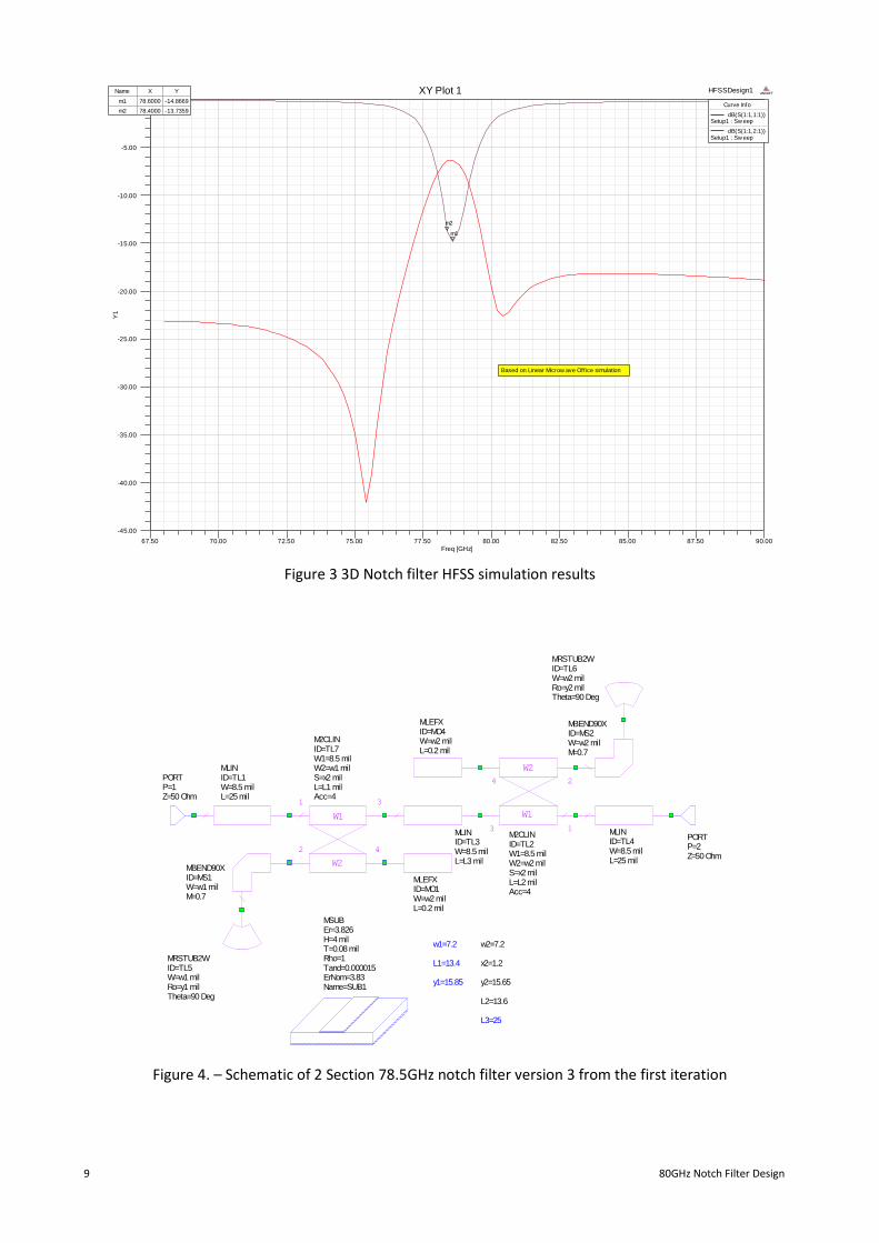
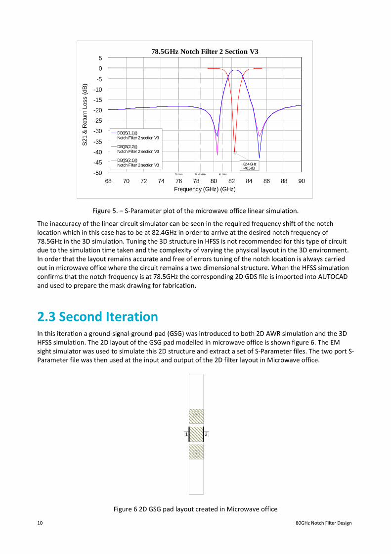
Shown next in figure 3 is the HFSS simulation of the 3D structure shown in Figure 2. The microwave office
circuit used to create the 3D HFSS structure shown in figure 4. The linear S-Parameter plot of this circuit in
microwave office is also shown in figure 5.
9 80GHz Notch Filter Design
Figure 3 3D Notch filter HFSS simulation results
Figure 4. – Schematic of 2 Section 78.5GHz notch filter version 3 from the first iteration
67.50 70.00 72.50 75.00 77.50 80.00 82.50 85.00 87.50 90.00Freq [GHz]
-45.00
-40.00
-35.00
-30.00
-25.00
-20.00
-15.00
-10.00
-5.00
0.00
Y1
HFSSDesign1XY Plot 1 ANSOFT
m1
m2
Based on Linear Microw ave Office simulation
Curve Info
dB(S(1:1,1:1))Setup1 : Sw eep
dB(S(1:1,2:1))Setup1 : Sw eep
Name X Y
m1 78.6000 -14.8669
m2 78.4000 -13.7359
W1
W2
1
2
3
4
M2CLINID=TL2W1=8.5 milW2=w2 milS=x2 milL=L2 milAcc=4
W1
W2
1
2
3
4
M2CLINID=TL7W1=8.5 milW2=w1 milS=x2 milL=L1 milAcc=4
MBEND90XID=MS1W=w1 milM=0.7
MBEND90XID=MS2W=w2 milM=0.7
MLEFXID=MO1W=w2 milL=0.2 mil
MLEFXID=MO4W=w2 milL=0.2 mil
MLINID=TL1W=8.5 milL=25 mil
MLINID=TL3W=8.5 milL=L3 mil
MLINID=TL4W=8.5 milL=25 mil
MRSTUB2WID=TL5W=w1 milRo=y1 milTheta=90 Deg
MRSTUB2WID=TL6W=w2 milRo=y2 milTheta=90 Deg
MSUBEr=3.826H=4 milT=0.08 milRho=1Tand=0.000015ErNom=3.83Name=SUB1
PORTP=1Z=50 Ohm
PORTP=2Z=50 Ohm
x2=1.2
y2=15.65
L2=13.6
L1=13.4
w1=7.2
y1=15.85
w2=7.2
L3=25
10 80GHz Notch Filter Design
Figure 5. – S-Parameter plot of the microwave office linear simulation.
The inaccuracy of the linear circuit simulator can be seen in the required frequency shift of the notch
location which in this case has to be at 82.4GHz in order to arrive at the desired notch frequency of
78.5GHz in the 3D simulation. Tuning the 3D structure in HFSS is not recommended for this type of circuit
due to the simulation time taken and the complexity of varying the physical layout in the 3D environment.
In order that the layout remains accurate and free of errors tuning of the notch location is always carried
out in microwave office where the circuit remains a two dimensional structure. When the HFSS simulation
confirms that the notch frequency is at 78.5GHz the corresponding 2D GDS file is imported into AUTOCAD
and used to prepare the mask drawing for fabrication.
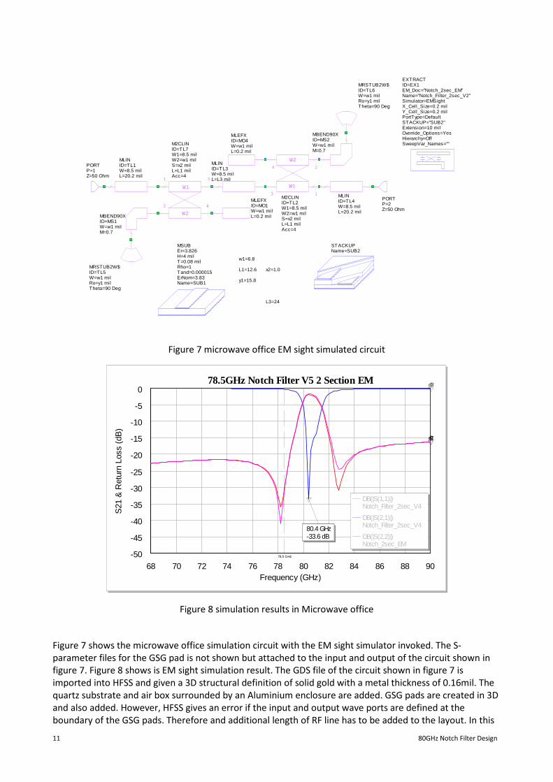
2.3 Second Iteration In this iteration a ground-signal-ground-pad (GSG) was introduced to both 2D AWR simulation and the 3D
HFSS simulation. The 2D layout of the GSG pad modelled in microwave office is shown figure 6. The EM
sight simulator was used to simulate this 2D structure and extract a set of S-Parameter files. The two port S-
Parameter file was then used at the input and output of the 2D filter layout in Microwave office.
Figure 6 2D GSG pad layout created in Microwave office
68 70 72 74 76 78 80 82 84 86 88 90Frequency (GHz) (GHz)
78.5GHz Notch Filter 2 Section V3
-50
-45
-40
-35
-30
-25
-20
-15
-10
-5
0
5
S21
& R
etur
n Lo
ss (
dB)
78.45 GHz 81 GHz76 GHz
82.4 GHz-40.5 dB
DB(|S(1,1)|)Notch Filter 2 section V3
DB(|S(2,2)|)Notch Filter 2 section V3
DB(|S(2,1)|)Notch Filter 2 section V3
21
11 80GHz Notch Filter Design
Figure 7 microwave office EM sight simulated circuit
Figure 8 simulation results in Microwave office
Figure 7 shows the microwave office simulation circuit with the EM sight simulator invoked. The S-
parameter files for the GSG pad is not shown but attached to the input and output of the circuit shown in
figure 7. Figure 8 shows is EM sight simulation result. The GDS file of the circuit shown in figure 7 is
imported into HFSS and given a 3D structural definition of solid gold with a metal thickness of 0.16mil. The
quartz substrate and air box surrounded by an Aluminium enclosure are added. GSG pads are created in 3D
and also added. However, HFSS gives an error if the input and output wave ports are defined at the
boundary of the GSG pads. Therefore and additional length of RF line has to be added to the layout. In this
STACKUPName=SUB2
EXTRACTID=EX1EM_Doc="Notch_2sec_EM"Name="Notch_Filter_2sec_V2"Simulator=EMSightX_Cell_Size=0.2 milY_Cell_Size=0.2 milPortType=DefaultSTACKUP="SUB2"Extension=10 milOverride_Options=YesHierarchy=OffSweepVar_Names=""
W1
W2
1
2
3
4
M2CLINID=TL2W1=8.5 milW2=w1 milS=x2 milL=L1 milAcc=4
W1
W2
1
2
3
4
M2CLINID=TL7W1=8.5 milW2=w1 milS=x2 milL=L1 milAcc=4
MBEND90XID=MS1W=w1 milM=0.7
MBEND90XID=MS2W=w1 milM=0.7
MLEFXID=MO1W=w1 milL=0.2 mil
MLEFXID=MO4W=w1 milL=0.2 mil
MLINID=TL1W=8.5 milL=20.2 mil
MLINID=TL3W=8.5 milL=L3 mil
MLINID=TL4W=8.5 milL=20.2 mil
MRSTUB2W$ID=TL5W=w1 milRo=y1 milTheta=90 Deg
MSUBEr=3.826H=4 milT=0.08 milRho=1Tand=0.000015ErNom=3.83Name=SUB1
MRSTUB2W$ID=TL6W=w1 milRo=y1 milTheta=90 Deg
PORTP=1Z=50 Ohm
PORTP=2Z=50 Ohm
x2=1.0
L3=24
w1=6.8
L1=12.6
y1=15.8
68 70 72 74 76 78 80 82 84 86 88 90Frequency (GHz)
78.5GHz Notch Filter V5 2 Section EM
-50
-45
-40
-35
-30
-25
-20
-15
-10
-5
0
S21
& R
etur
n Lo
ss (
dB)
d3
d2d1
78.5 GHz
80.4 GHz-33.6 dB
DB(|S(1,1)|)Notch_Filter_2sec_V4
DB(|S(2,1)|)Notch_Filter_2sec_V4
DB(|S(2,2)|)Notch_2sec_EM
12 80GHz Notch Filter Design
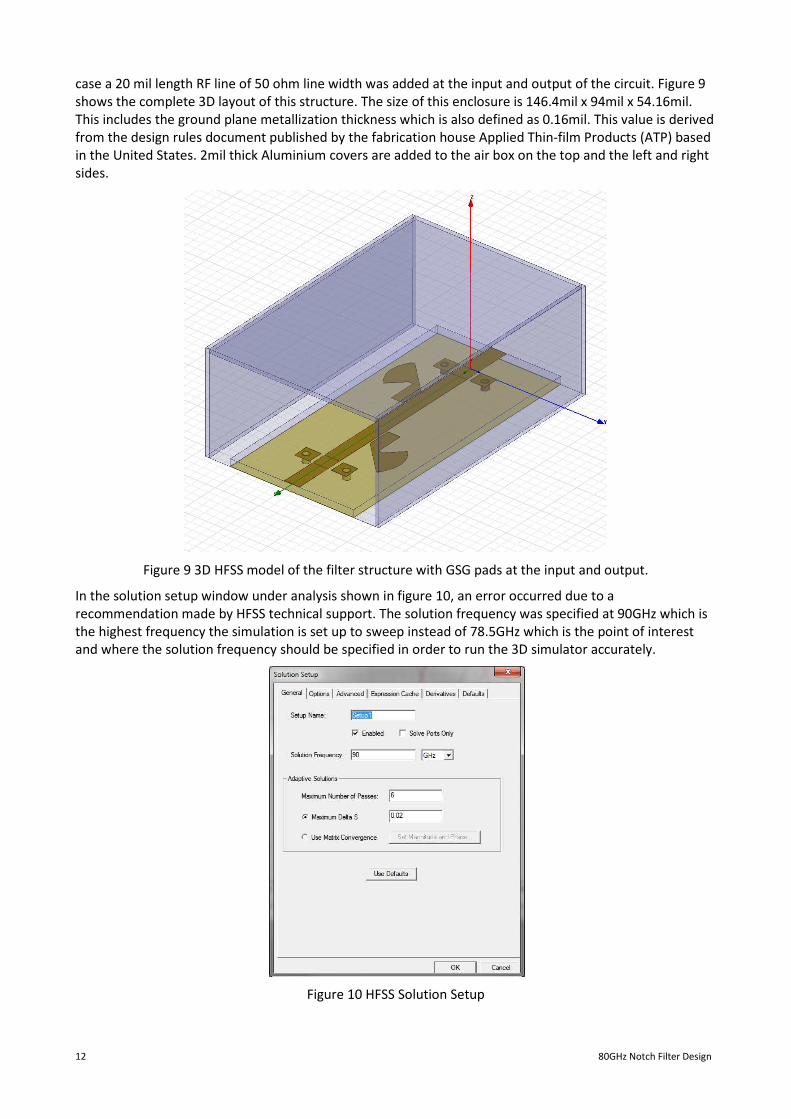
case a 20 mil length RF line of 50 ohm line width was added at the input and output of the circuit. Figure 9
shows the complete 3D layout of this structure. The size of this enclosure is 146.4mil x 94mil x 54.16mil.
This includes the ground plane metallization thickness which is also defined as 0.16mil. This value is derived
from the design rules document published by the fabrication house Applied Thin-film Products (ATP) based
in the United States. 2mil thick Aluminium covers are added to the air box on the top and the left and right
sides.
Figure 9 3D HFSS model of the filter structure with GSG pads at the input and output.
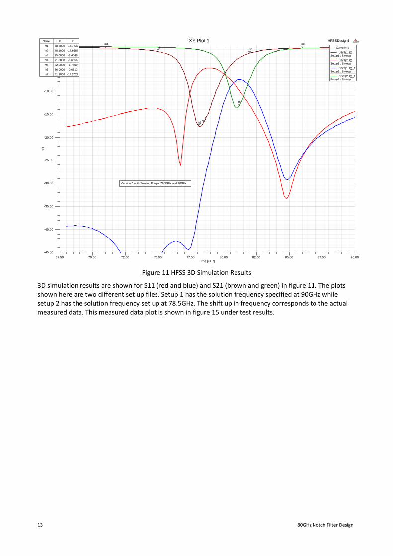
In the solution setup window under analysis shown in figure 10, an error occurred due to a
recommendation made by HFSS technical support. The solution frequency was specified at 90GHz which is
the highest frequency the simulation is set up to sweep instead of 78.5GHz which is the point of interest
and where the solution frequency should be specified in order to run the 3D simulator accurately.
Figure 10 HFSS Solution Setup
13 80GHz Notch Filter Design
Figure 11 HFSS 3D Simulation Results
3D simulation results are shown for S11 (red and blue) and S21 (brown and green) in figure 11. The plots
shown here are two different set up files. Setup 1 has the solution frequency specified at 90GHz while
setup 2 has the solution frequency set up at 78.5GHz. The shift up in frequency corresponds to the actual
measured data. This measured data plot is shown in figure 15 under test results.
67.50 70.00 72.50 75.00 77.50 80.00 82.50 85.00 87.50 90.00Freq [GHz]
-45.00
-40.00
-35.00
-30.00
-25.00
-20.00
-15.00
-10.00
-5.00
0.00Y
1HFSSDesign1XY Plot 1 ANSOFT
m1
m2
m3m4
m5
m6
m7
Version 5 w ith Solution Freq at 78.5GHz and 90GHz
Curve Info
dB(S(1,1))Setup1 : Sw eep
dB(S(2,1))Setup1 : Sw eep
dB(S(1,1))_1Setup2 : Sw eep
dB(S(2,1))_1Setup2 : Sw eep
Name X Y
m1 78.5000 -16.7737
m2 78.1000 -17.6657
m3 75.0000 -1.4546
m4 71.0000 -0.6556
m5 82.0000 -1.7869
m6 86.0000 -0.6612
m7 81.2000 -13.2029
14 80GHz Notch Filter Design
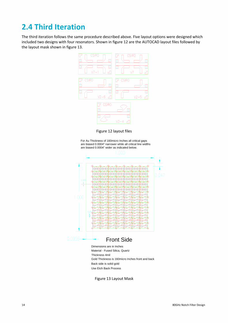
2.4 Third Iteration The third iteration follows the same procedure described above. Five layout options were designed which
included two designs with four resonators. Shown in figure 12 are the AUTOCAD layout files followed by
the layout mask shown in figure 13.
Figure 12 layout files
Figure 13 Layout Mask
Front SideDimensions are in Inches
Material - Fused Silica, Quartz
Thickness 4milGold Thickness is 160micro Inches front and back
Back side is solid gold
Use Etch Back Process
For Au Thickness of 160micro Inches all critical gapsare biased 0.0004" narrower while all critical line widthsare biased 0.0004" wider as indicated below.
15 80GHz Notch Filter Design
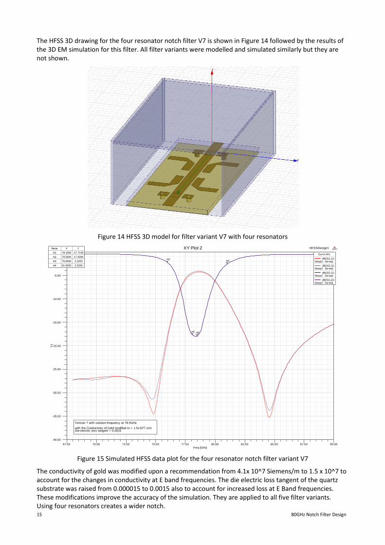
The HFSS 3D drawing for the four resonator notch filter V7 is shown in Figure 14 followed by the results of
the 3D EM simulation for this filter. All filter variants were modelled and simulated similarly but they are
not shown.
Figure 14 HFSS 3D model for filter variant V7 with four resonators
Figure 15 Simulated HFSS data plot for the four resonator notch filter variant V7
The conductivity of gold was modified upon a recommendation from 4.1x 10^7 Siemens/m to 1.5 x 10^7 to
account for the changes in conductivity at E band frequencies. The die electric loss tangent of the quartz
substrate was raised from 0.000015 to 0.0015 also to account for increased loss at E Band frequencies.
These modifications improve the accuracy of the simulation. They are applied to all five filter variants.
Using four resonators creates a wider notch.
67.50 70.00 72.50 75.00 77.50 80.00 82.50 85.00 87.50 90.00Freq [GHz]
-40.00
-35.00
-30.00
-25.00
-20.00
-15.00
-10.00
-5.00
0.00
Y1
HFSSDesign1XY Plot 2 ANSOFT
m1 m2
m3 m4
Version 7 with solution frequency at 78.5GHz with the Conductivity of Gold modified to = 1.5x10 7̂ s/mDie-electric loss tangent = 0.0015
Curve Info
dB(S(1,1))Setup2 : Sw eep
dB(S(2,2))Setup2 : Sw eep
dB(S(2,1))Setup2 : Sw eep
dB(S(1,2))Setup2 : Sw eep
Name X Y
m1 78.1000 -17.7149
m2 78.5000 -17.9296
m3 76.0000 -2.3253
m4 81.0000 -2.6255

16 80GHz Notch Filter Design
3. Test Results
Figure 16 Plotted test data for Filter variant V5EM
Figure 15 shows the plotted test data for the notch filter from the second iteration discussed above in
section 3.3. The 3D HFSS simulation of this filter was shown in figure 11. In this simulation the setup 2
simulation data plotted out corresponds to the actual test data. Maker m7 in figure 11 is at 81.2GHz. This
reveals the close agreement of the simulation data to the test data once the error in the solution frequency
of the HFSS simulation was eliminated.
70 71 72 73 74 75 76 77 78 79 80 81 82 83 84 85 86 87 88 89 90Frequency (GHz)
Notch Filter V5EM
-40
-35
-30
-25
-20
-15
-10
-5
0
81.2 GHz78.5 GHz76 GHz
76 GHz-0.6578 dB
71 GHz-0.5853 dB
81.2 GHz-14.29 dB
DB(|S(1,1)|)V5EM 1.$FPRJ
DB(|S(2,1)|)V5EM 1
DB(|S(2,2)|)V5EM 1.$FPRJ
17 80GHz Notch Filter Design
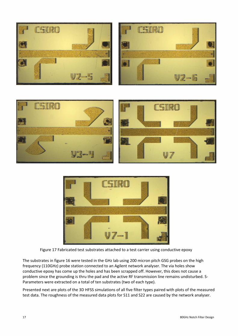
Figure 17 Fabricated test substrates attached to a test carrier using conductive epoxy
The substrates in figure 16 were tested in the GHz lab using 200 micron pitch GSG probes on the high
frequency (110GHz) probe station connected to an Agilent network analyser. The via holes show
conductive epoxy has come up the holes and has been scrapped off. However, this does not cause a
problem since the grounding is thru the pad and the active RF transmission line remains undisturbed. S-
Parameters were extracted on a total of ten substrates (two of each type).
Presented next are plots of the 3D HFSS simulations of all five filter types paired with plots of the measured
test data. The roughness of the measured data plots for S11 and S22 are caused by the network analyser.
18 80GHz Notch Filter Design
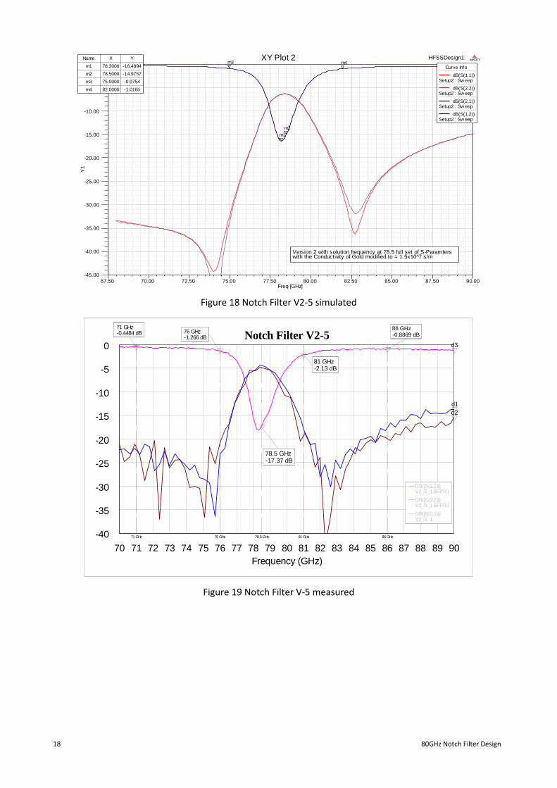
Figure 18 Notch Filter V2-5 simulated
Figure 19 Notch Filter V-5 measured
67.50 70.00 72.50 75.00 77.50 80.00 82.50 85.00 87.50 90.00Freq [GHz]
-45.00
-40.00
-35.00
-30.00
-25.00
-20.00
-15.00
-10.00
-5.00
0.00
Y1
HFSSDesign1XY Plot 2 ANSOFT
m1
m2
m3 m4
Version 2 with solution frequency at 78.5 full set of S-Paramterswith the Conductivity of Gold modified to = 1.5x10^7 s/m
Curve Info
dB(S(1,1))Setup2 : Sw eep
dB(S(2,2))Setup2 : Sw eep
dB(S(2,1))Setup2 : Sw eep
dB(S(1,2))Setup2 : Sw eep
Name X Y
m1 78.2000 -16.4894
m2 78.5000 -14.9757
m3 75.0000 -0.9754
m4 82.0000 -1.0165
70 71 72 73 74 75 76 77 78 79 80 81 82 83 84 85 86 87 88 89 90Frequency (GHz)
Notch Filter V2-5
-40
-35
-30
-25
-20
-15
-10
-5
0 d3
d2d1
71 GHz 86 GHz81 GHz78.5 GHz76 GHz
86 GHz-0.8869 dB
81 GHz-2.13 dB
71 GHz-0.4484 dB 76 GHz
-1.266 dB
78.5 GHz-17.37 dB
DB(|S(1,1)|)V2_5_1.$FPRJ
DB(|S(2,2)|)V2_5_1.$FPRJ
DB(|S(2,1)|)V2_5_1
19 80GHz Notch Filter Design
Figure 20 Notch Filter V2-6 simulated
Figure 21 Notch Filter V2-6 measured
In the simulation of this filter the notch location was offset 400 MHz lower to 78.1GHz. This was done in
anticipation of a slight drift of the frequency due to variations in the fabrication process. However, no such
variations can be seen from the measured data.
67.50 70.00 72.50 75.00 77.50 80.00 82.50 85.00 87.50 90.00Freq [GHz]
-45.00
-40.00
-35.00
-30.00
-25.00
-20.00
-15.00
-10.00
-5.00
0.00
Y1
HFSSDesign1XY Plot 2 ANSOFT
m1
m2
m3 m4
Version 2 w ith solution f rw equency at 78.5 full set of S-Paramtersw ith the Conductivity of Gold modif ied to = 1.5x10^7 s/m
Curve Info
dB(S(1,1))Setup2 : Sw eep
dB(S(2,2))Setup2 : Sw eep
dB(S(2,1))Setup2 : Sw eep
dB(S(1,2))Setup2 : Sw eep
Name X Y
m1 78.1000 -14.7809
m2 78.5000 -12.2902
m3 75.0000 -0.9520
m4 82.0000 -0.8388
70 71 72 73 74 75 76 77 78 79 80 81 82 83 84 85 86 87 88 89 90Frequency (GHz)
Notch Filter V2-6
-40
-35
-30
-25
-20
-15
-10
-5
0
71 GHz 86 GHz81 GHz78.5 GHz76 GHz
78.1 GHz-16.14 dB
86 GHz-1.041 dB
81 GHz-1.694 dB
71 GHz-0.478 dB
76 GHz-1.342 dB
78.5 GHz-14.96 dB
DB(|S(1,1)|)V2_6_1.$FPRJ
DB(|S(2,1)|)V2_6_1
DB(|S(2,2)|)V2_6_1.$FPRJ
20 80GHz Notch Filter Design
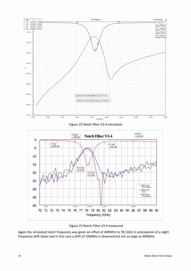
Figure 22 Notch filter V3-4 simulated
Figure 23 Notch Filter V3-4 measured
Again the simulated notch frequency was given an offset of 400MHz to 78.1GHz in anticipation of a slight
frequency drift lower and in this case a drift of 100MHz is observed but not as large as 400MHz.
67.50 70.00 72.50 75.00 77.50 80.00 82.50 85.00 87.50 90.00Freq [GHz]
-45.00
-40.00
-35.00
-30.00
-25.00
-20.00
-15.00
-10.00
-5.00
0.00
Y1
HFSSDesign1XY Plot 2 ANSOFT
m1
m2
m3 m4
Conductivity of Gold Modified to 1.5x10 7̂ s/m
Version 3.4 with solution frequency at 78.5GHz
Curve Info
dB(S(1,1))Setup2 : Sw eep
dB(S(2,2))Setup2 : Sw eep
dB(S(2,1))Setup2 : Sw eep
dB(S(1,2))Setup2 : Sw eep
Name X Y
m1 78.1000 -14.1395
m2 78.5000 -11.2408
m3 75.0000 -1.0737
m4 82.0000 -0.8142
70 71 72 73 74 75 76 77 78 79 80 81 82 83 84 85 86 87 88 89 90Frequency (GHz)
Notch Filter V3-4
-40
-35
-30
-25
-20
-15
-10
-5
0
71 GHz 86 GHz81 GHz78.5 GHz76 GHz
78.2 GHz-15.65 dB
78.5 GHz-14.13 dB
76 GHz-1.399 dB
71 GHz-0.4969 dB
86 GHz-1.043 dB
81 GHz-1.601 dB
DB(|S(1,1)|)V3_4_1.$FPRJ
DB(|S(2,1)|)V3_4_1
DB(|S(2,2)|)V3_4_1.$FPRJ
21 80GHz Notch Filter Design
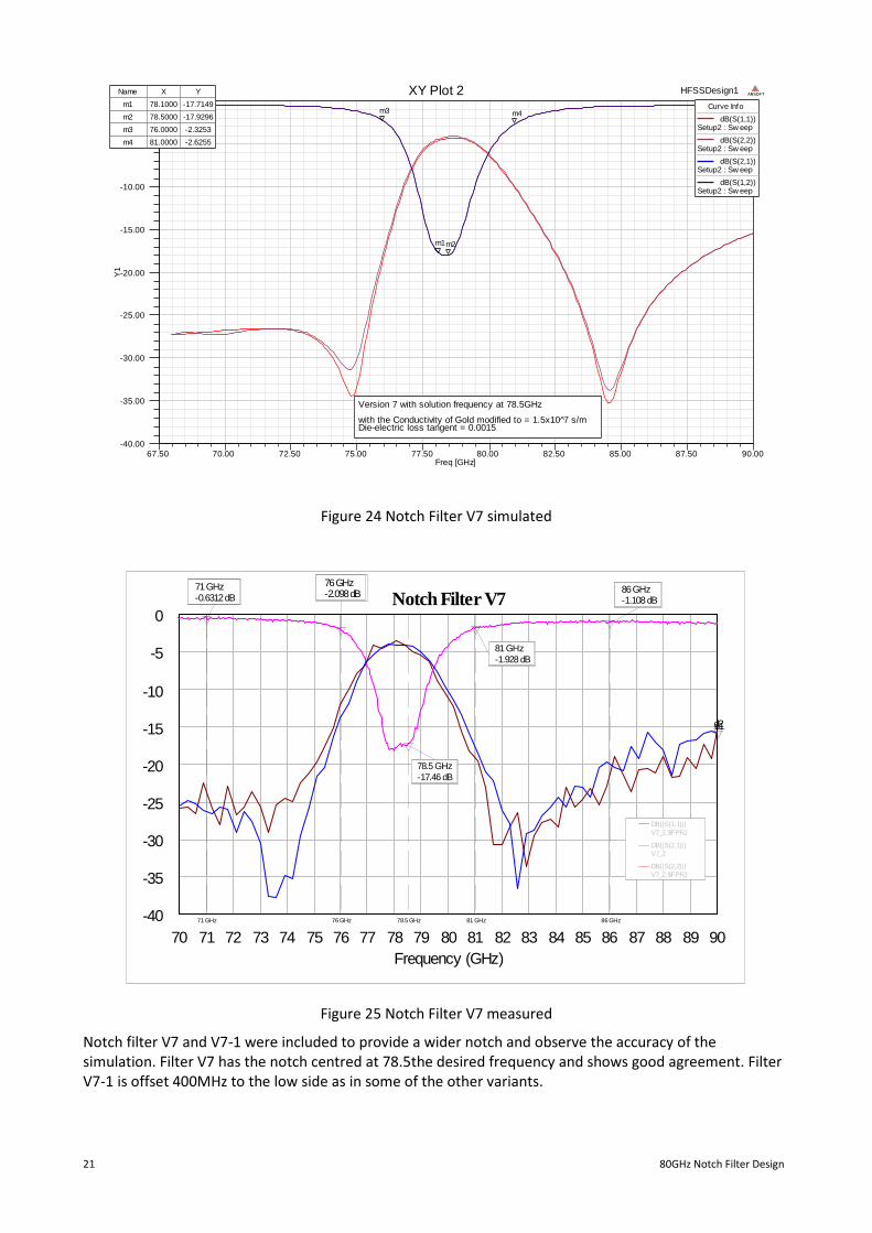
Figure 24 Notch Filter V7 simulated
Figure 25 Notch Filter V7 measured
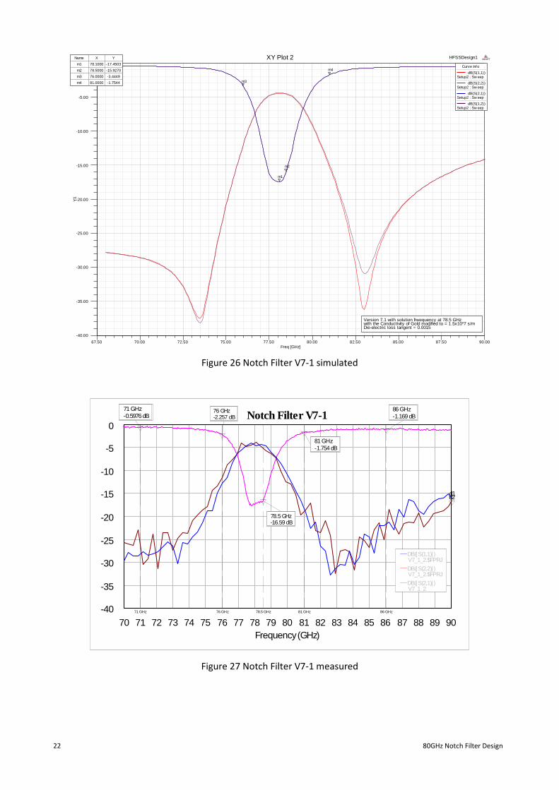
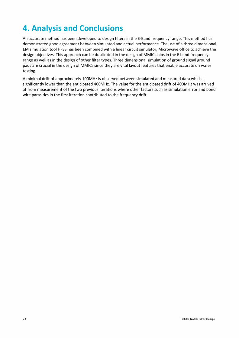
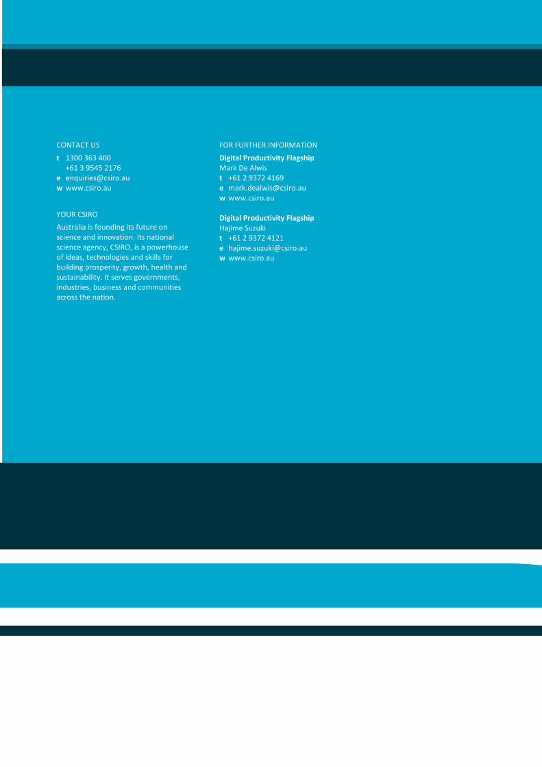
Notch filter V7 and V7-1 were included to provide a wider notch and observe the accuracy of the
simulation. Filter V7 has the notch centred at 78.5the desired frequency and shows good agreement. Filter
V7-1 is offset 400MHz to the low side as in some of the other variants.
67.50 70.00 72.50 75.00 77.50 80.00 82.50 85.00 87.50 90.00Freq [GHz]
-40.00
-35.00
-30.00
-25.00
-20.00
-15.00
-10.00
-5.00
0.00
Y1
HFSSDesign1XY Plot 2 ANSOFT
m1m2
m3 m4
Version 7 with solution frequency at 78.5GHz with the Conductivity of Gold modified to = 1.5x10 7̂ s/mDie-electric loss tangent = 0.0015
Curve Info
dB(S(1,1))Setup2 : Sw eep
dB(S(2,2))Setup2 : Sw eep
dB(S(2,1))Setup2 : Sw eep
dB(S(1,2))Setup2 : Sw eep
Name X Y
m1 78.1000 -17.7149
m2 78.5000 -17.9296
m3 76.0000 -2.3253
m4 81.0000 -2.6255
70 71 72 73 74 75 76 77 78 79 80 81 82 83 84 85 86 87 88 89 90Frequency (GHz)
Notch Filter V7
-40
-35
-30
-25
-20
-15
-10
-5
0
d2d1
71 GHz 86 GHz81 GHz78.5 GHz76 GHz
86 GHz-1.108 dB
81 GHz-1.928 dB
71 GHz-0.6312 dB
76 GHz-2.098 dB
78.5 GHz-17.46 dB
DB(|S(1,1)|)V7_2.$FPRJ
DB(|S(2,1)|)V7_2
DB(|S(2,2)|)V7_2.$FPRJ
22 80GHz Notch Filter Design
Figure 26 Notch Filter V7-1 simulated
Figure 27 Notch Filter V7-1 measured
67.50 70.00 72.50 75.00 77.50 80.00 82.50 85.00 87.50 90.00Freq [GHz]
-40.00
-35.00
-30.00
-25.00
-20.00
-15.00
-10.00
-5.00
0.00
Y1
HFSSDesign1XY Plot 2 ANSOFT
m1
m2
m3
m4
Version 7.1 with solution frwequency at 78.5 GHz with the Conductivity of Gold modified to = 1.5x10^7 s/mDie-electric loss tangent = 0.0015
Curve Info
dB(S(1,1))Setup2 : Sw eep
dB(S(2,2))Setup2 : Sw eep
dB(S(2,1))Setup2 : Sw eep
dB(S(1,2))Setup2 : Sw eep
Name X Y
m1 78.1000 -17.4503
m2 78.5000 -15.9270
m3 76.0000 -3.4449
m4 81.0000 -1.7544
70 71 72 73 74 75 76 77 78 79 80 81 82 83 84 85 86 87 88 89 90Frequency (GHz)
Notch Filter V7-1
-40
-35
-30
-25
-20
-15
-10
-5
0
d2d1
71 GHz 86 GHz81 GHz78.5 GHz76 GHz
86 GHz-1.169 dB
81 GHz-1.754 dB
71 GHz-0.5976 dB
76 GHz-2.257 dB
78.5 GHz-16.59 dB
DB(|S(1,1)| )V7_1_2.$FPRJ
DB(|S(2,2)| )V7_1_2.$FPRJ
DB(|S(2,1)| )V7_1_2
23 80GHz Notch Filter Design
4. Analysis and Conclusions An accurate method has been developed to design filters in the E-Band frequency range. This method has
demonstrated good agreement between simulated and actual performance. The use of a three dimensional
EM simulation tool HFSS has been combined with a linear circuit simulator, Microwave office to achieve the
design objectives. This approach can be duplicated in the design of MMIC chips in the E band frequency
range as well as in the design of other filter types. Three dimensional simulation of ground signal ground
pads are crucial in the design of MMICs since they are vital layout features that enable accurate on wafer
testing.
A minimal drift of approximately 100MHz is observed between simulated and measured data which is
significantly lower than the anticipated 400MHz. The value for the anticipated drift of 400MHz was arrived
at from measurement of the two previous iterations where other factors such as simulation error and bond
wire parasitics in the first iteration contributed to the frequency drift.
24 80GHz Notch Filter Design
CONTACT US
t 1300 363 400
+61 3 9545 2176
w www.csiro.au
YOUR CSIRO
Australia is founding its future on
science and innovation. Its national
science agency, CSIRO, is a powerhouse
of ideas, technologies and skills for
building prosperity, growth, health and
sustainability. It serves governments,
industries, business and communities
across the nation.
FOR FURTHER INFORMATION
Digital Productivity Flagship
Mark De Alwis
t +61 2 9372 4169
w www.csiro.au
Digital Productivity Flagship
Hajime Suzuki
t +61 2 9372 4121
w www.csiro.au