8051 Training Kit Labbook - robotshop.com · All trademarked names in this manual are the property...
33
8051 Training Kit Lab Book Date: 10th April, 2005 Document Revision: 1.04 BiPOM Electronics 16301 Blue Ridge Road, Missouri City, Texas 77489 USA Telephone: (713) 283-9970 Fax: (281) 416 - 2806 E-mail: [email protected] Web: www.bipom.com
Transcript of 8051 Training Kit Labbook - robotshop.com · All trademarked names in this manual are the property...

8051 Training Kit Lab Book
Date: 10th April, 2005 Document Revision: 1.04
BiPOM Electronics 16301 Blue Ridge Road, Missouri City, Texas 77489 USA Telephone: (713) 283-9970 Fax: (281) 416 - 2806 E-mail: [email protected] Web: www.bipom.com

8051 Training Lab
Page 2
© 1999-2005 by BiPOM Electronics, Inc. All rights reserved. 8051 Training Kit Training Lab Student Exercise Book. No part of this work may be reproduced in any manner without written permission of BiPOM Electronics. All trademarked names in this manual are the property of respective owners. WARRANTY: BiPOM Electronics warrants 8051 Training Kit for a period of 90 days. If the Kit becomes defective during this period, BiPOM Electronics will at its option, replace or repair the Kit. This warranty is voided if the product is subjected to physical abuse or operated outside stated electrical limits. BiPOM Electronics will not be responsible for damage to any external devices connected to the Kit. BiPOM Electronics disclaims all warranties express or implied warranties of merchantability and fitness for a particular purpose. In no event shall BiPOM Electronics be liable for any indirect, special, incidental or consequential damages in connection with or arising from the use of this product. BiPOM’s liability is limited to the purchase price of this product.
8051 Training Lab
Page 3
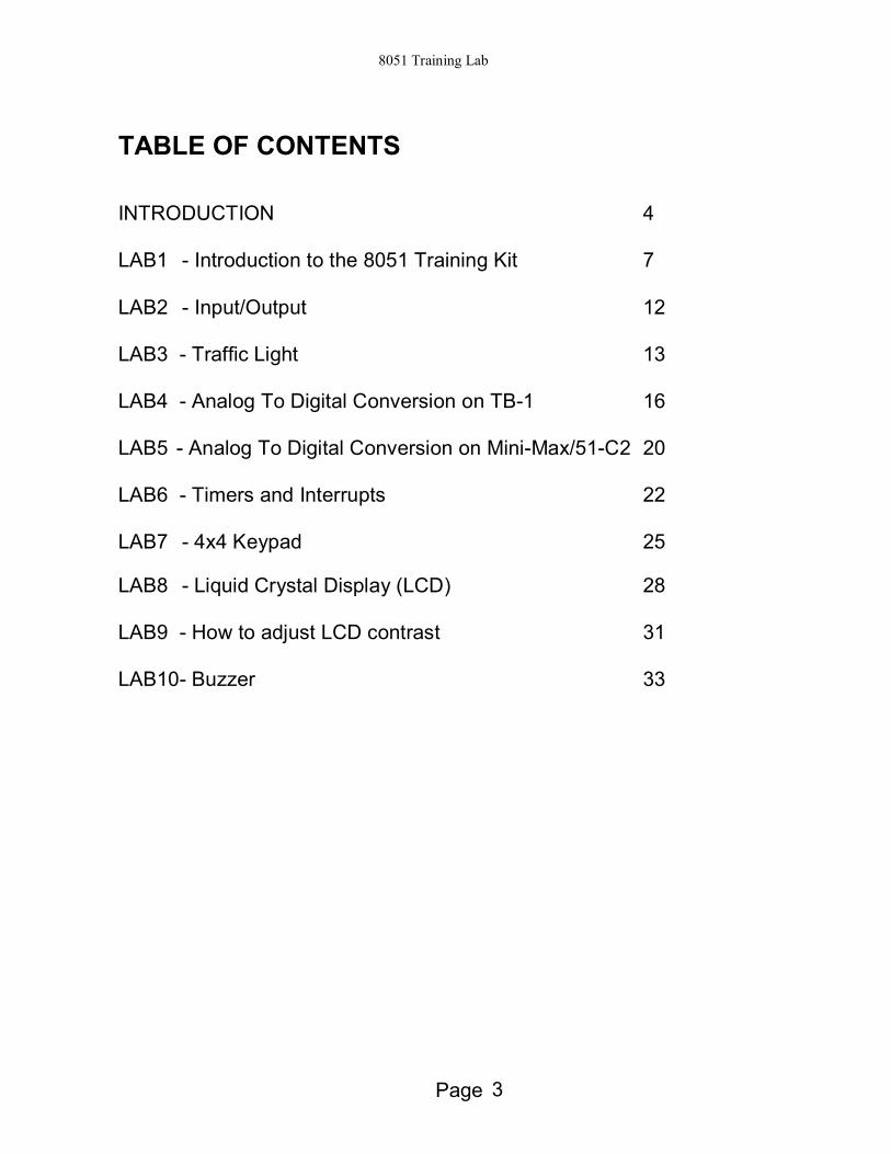
TABLE OF CONTENTS INTRODUCTION 4 LAB1 - Introduction to the 8051 Training Kit 7 LAB2 - Input/Output 12 LAB3 - Traffic Light 13 LAB4 - Analog To Digital Conversion on TB-1 16 LAB5 - Analog To Digital Conversion on Mini-Max/51-C2 20 LAB6 - Timers and Interrupts 22 LAB7 - 4x4 Keypad 25
LAB8 - Liquid Crystal Display (LCD) 28 LAB9 - How to adjust LCD contrast 31 LAB10- Buzzer 33

8051 Training Lab
Page 4
Introduction The purpose of the 8051 Training Lab is to familiarize the student with developing practical applications using the ATMEL AT89C51ED2 series of micro-controllers. AT89C51ED2 is based on the Intel 8051 micro-controller architecture, the most widely used micro-controller system with applications ranging from industrial, medical, home automation to automotive. The 8051 Training Kit consists of the following components: • MicroTRAK Carrier Board • MINI-MAX/51-C2 Microcontroller Board • TB-1 Training Board • PROTO-1 Prototyping Board • 8051 I/O Module • LCD242 LCD • KP1-4X4 Keypad • Demo versions of BASCOM51 BASIC Compiler • Demo versions of Micro C Compiler/Linker/Assembler • Micro-IDE Integrated Development Environment/Simulator/Offline Debugger • Full version of SDCC C Compiler (open-source) • Over 70 example projects • Serial downloader(WinLoad). • Cables • Adapter • Training Manuals • Labbook The following external items are required for each training kit station: • IBM Compatible Personal Computer (PC) running Windows 95/98/XP or NT 4.0.
(8051 Training Kit will not work with DOS, Windows 3.1 or lower ). Minimum 16MB memory and 10 MB of available hard disk space.
• One available RS232 Serial port ( COM1 through COM8 ). Figure 1 shows all the components connected together.

8051 Training Lab
Page 5
To outlet
RS232 Serial Cable
Mini-Max/51-C2 TB-1 DAQ127
LCD242
8051 I/O Module MicroTRAK/51-C2KP1-4X4 Keypad
Figure 1
Getting Started Log on to Windows before using the 8051 Training Kit. Enter the user name and password that your instructor has given to you before the Lab. Make sure to log out when you are done with the PC at the end of the Lab. Do not share your username or password with anybody. The programs are written as C and BASIC Language Program files ( with the extension .C or .BAS but they are plain text files ). These C and BASIC Program files are created using Micro-IDE Integrated Development Environment for Windows. You can edit and save programs and download to the Training Board using Micro-IDE. Creating programs and running them on the Training Board consists of the following steps: 1. Edit an existing or create a new program using Micro-IDE Program Editor. 2. Compile the program using Micro-IDE Build Toolkit (C Compiler) 3. Download the program to the Training Board using Micro-IDE Serial Loader. 4. Run and debug the program on the Training Board using Micro-IDE Terminal Window. Figure 3 illustrates these steps.

8051 Training Lab
Page 6
Figure 3.
Create 80C51 C Programs
Compile Using C Compiler
Download to 80C51 Training Kit
Execute program

8051 Training Lab
Page 7
LAB1 – Introduction to the 8051 Training Kit Overview The purpose of this lab is to familiarize you with the 8051 Training Kit and the program development environment. In this lab, you will create a simple program in C language, compile the program to form a hex file, download the program to the MINI-MAX/51-C2 Microcontroller board and execute the program. The knowledge developed in this lab will be very useful in subsequent labs when working with the ATMEL AT89C51ED2 single-chip flash micro-controller to develop programs. Instructions To create your own project, select Project menu and select New Project. This will display the New Project dialog. Enter the name of the new project and its location ( this example uses test as the project name and c:\test as the project location ). Toolkit is already pre-selected as Micro C 8051-8052. Click OK; the new project with the name of test under c:\test will be created.
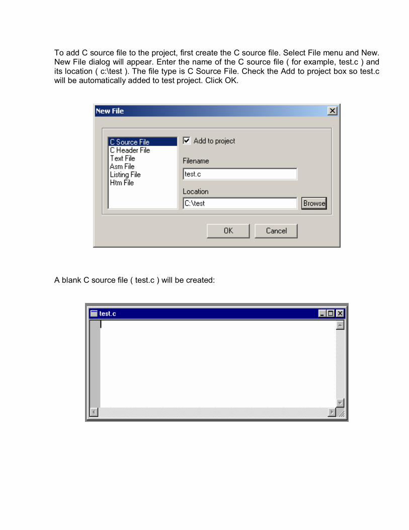
To add C source file to the project, first create the C source file. Select File menu and New. New File dialog will appear. Enter the name of the C source file ( for example, test.c ) and its location ( c:\test ). The file type is C Source File. Check the Add to project box so test.c will be automatically added to test project. Click OK.
A blank C source file ( test.c ) will be created:

8051 Training Lab
Page 9
Type the following lines which are the header files required by the Micro C Compiler: #include <8051io.h> #include <8051bit.h> #include <8051reg.h> Then type the following small C program: void main() { serinit(19200>>1); printf( “\nHello World” ); while(1); } The C source file should now look like this:
This program prints “Hello World” on the terminal window. The program then enters an infinite loop. Build the program by clicking the Build button. You will be prompted to save the file. Click Yes. If the program builds successfully, you will see the following messages on the Output Window: Compiling c:\test\test.c… Linking test.asm … Generating Output… First pass… Second pass… 0 error(s)

8051 Training Lab
Page 10
You can download the program to the board by clicking the Download button on the main toolbar:
If the board is powered and connected properly to the PC, a progress dialog will appear:
The progress dialog will disappear following a successful download. You can see the details of the download by selecting the Loader Tab on the Output Window
If there is an error during download, check the following:
1. Is the power adapter plugged to the 8051 Training Kit ? 2. Is the serial cable securely attached to the 8051 Training Kit ? 3. Is the serial cable securely attached to the PC ?
Download
Loader Tab

8051 Training Lab
Page 11
After the program has been successful downloaded, it can be started using the Mode button on the main Toolbar:
Mode button puts the board into the Run mode or the Program mode. In Run mode, the micro-controller is executing the program in its memory. In Program mode, the micro-controller is in Reset state so no programs are running. In Program mode, micro-controller’s flash memory can be changed and a new program can be downloaded. The Mode button is Red in Program mode and Green in Run mode. Following a download, the Mode button will be Red. Click the Mode button to change the mode to Run mode. The program ( test.c ) that you just downloaded starts executing and prints the message “Hello World” on the terminal window. Click the Mode button once again so it turns Red. The board is now in Program mode.
Mode

8051 Training Lab
Page 12
LAB2 – Input/Output Overview This lab will familiarize you with the 8051 I/O Module included in 8051 Training Kit for monitoring and control all I/O ports of the microcontroller. Information 8051 I/O Module allows access to all input/output (I/O) ports of the 8051 micro-controller on the MicroTRAK development platform. 8051 I/O Module has 32 switches to control the 8051 micro-controller inputs and 32 LED’s to indicate the port statuses as logic LOW or logic HIGH.
Signal LED Switch Signal LED Switch P0.0 HL1 S1-1 P1.0 HL17 S2-1 P0.1 HL3 S1-2 P1.1 HL19 S2-2 P0.2 HL5 S1-3 P1.2 HL21 S2-3 P0.3 HL7 S1-4 P1.3 HL23 S2-4 P0.4 HL9 S1-5 P1.4 HL25 S2-5 P0.5 HL13 S1-6 P1.5 HL27 S2-6 P0.6 HL15 S1-7 P1.6 HL29 S2-7 P0.7 HL17 S1-8 P1.7 HL31 S2-8
Signal LED Switch Signal LED Switch P2.0 HL2 S3-1 P3.0 HL18 S4-1 P2.1 HL4 S3-2 P3.1 HL20 S4-2 P2.2 HL6 S3-3 P3.2 HL22 S4-3 P2.3 HL8 S3-4 P3.3 HL24 S4-4 P2.4 HL10 S3-5 P3.4 HL26 S4-5 P2.5 HL12 S3-6 P3.5 HL28 S4-6 P2.6 HL14 S3-7 P3.6 HL30 S4-7 P2.7 HL16 S3-8 P3.7 HL32 S4-8
Exercise Write a C program that turns on consistently all LED's connected to the corresponding ports(P0…P3) and reads status on the corresponding switches. NOTE: There are a few "special" port pins you can change status ( by switches, or by software), but this can disturb normal work of the setup. Special ports : P1.5, P1.6, P1.7, P3.0 and P3.1 For example: If you put P3.0 or P3.1 in logical "0" you will break serial communication with your PC!

8051 Training Lab
Page 13
LAB3 – Traffic Light Overview The purpose of this lab is to control the outputs of the micro-controller in a given sequence. Green, yellow and red Light Emitting Diodes (LED’s) on the TB-1 board are connected to micro-controller outputs. First, write a program to turn on only one LED and then turn off the same LED, Then, improve the program make the LED blink. The next part of the lab is to read the input switches. As switches are mechanical objects, some de-bounce time (dead time) will also be placed in the program. You will control an LED with one switch; as long as switch is active the respective LED is On and when switch is inactive, the corresponding LED is Off. Then, the LED will be made to blink as long as switch is On. Finally, you will write a little traffic light controller where the green, red, yellow LED's on the TB-1 board simulate the traffic lights and the switches simulate the car presence sensors at a crossroad. Information Most of the micro-controller pins and the power supply are available on the 20-pin connector (J3) for interfacing to external circuitry, prototyping boards and peripheral boards, including the TB-1 Training Board. Table 2 shows the J3 pin-out of the micro-controller pins.
MINI-MAX/51-C2 Expansion (J3)
Signal Pin Pin Signal P3.0 20 19 P3.1 P3.2 18 17 P3.3 P3.4 16 15 P3.5 P3.6 14 13 P3.7 P1.0 12 11 P1.1 P1.2 10 9 P1.3 P1.4 8 7 P1.5 P1.6 6 5 P1.7 VCC 4 3 GND VCC 2 1 GND
Table 2.

8051 Training Lab
Page 14
Two ports ( P1 and P3 ) of the micro-controller are accessible via the J3 connector. TB-1, which is connected to the micro-controller board as explained in Lab1, will be used as it already has input switches and output LED’s connected. Table 3 describes the pin-out on the J3 connector and their designation as respective to input (switches) or output (LED’s).
Micro-controller Pin
Connector on J3 Input or Output P3.2 18 Input, active Low, SW1 P3.3 17 Input, active Low, SW2 P1.3 9 Output, active High, Red LED P1.1 11 Output, active High, Yellow LED P1.0 12 Output, active High, Green LED
Table 3.
The term active low indicates that the micro-controller must be programmed in a manner such that the switch is made or activated when P3.2 or P3.3 read low logic. Correspondingly the term active high means that to activate an LED the corresponding micro-controller pin must generate high logic. The port directional register defines the state (input or output) of the micro-controller I/O lines. Exercise Initially turn the individual LED’s On and Off without interaction with the switches. Write a program to: • Turn Red LED On only for a brief time interval and than Off • Turn Yellow LED On only for a brief time interval and than Off • Turn Green LED On only for a brief time interval and than Off • Blink Red LED only • Blink all three LED’s You now have the capability of controlling more than one output line. Next step is to read an input line. When the Switch is not activated the respective line is high and an LED should be turned On. When the Switch is activated, blink an LED: • Turn Red Led On if Switch 1 is inactive. • Turn Yellow Led On if Switch 2 is inactive. • Blink Red Led as long as Switch 1 is active and Red Led is On if Switch 1 is inactive. • Blink Yellow Led as long as Switch 2 is active and Yellow Led is On if Switch 2 is
inactive.

8051 Training Lab
Page 15
Write a program to generate the results shown in Table 4 for a traffic light controller:
Switch 1 Switch 2 Red LED Yellow LED Green LED Open Open OFF OFF ON Open Closed ON ON OFF
Closed Open OFF OFF ON Closed Closed OFF OFF OFF
Table 4. Build the program and download to the Training Board. Trace through the program and watch the LED’s as you step through each instruction. Open and close Switch 1 and Switch 2 to change the LED’s to make sure that your program is handling every case correctly.

8051 Training Lab
Page 16
LAB4 – Analog To Digital Conversion on TB-1 Overview This lab is used to familiarize you with the operation of an A/D converter. A varying voltage is applied to the input of the A/D converter by using a potentiometer and its output is read into the micro-controller and displayed on the terminal screen. The A/D and the potentiometer are connected the Analog Input terminal blocks of TB-1. LM35 type temperature sensor will then be connected to the A/D and temperature values will be displayed on the board. Information Voltages that continuously vary as a function of time are defined as analog voltages and can have any value within certain range, e.g. 0V to 5V, or –5V to + 5V, or 0V to +12V etc. Digital voltages only have two values i.e. a 1 or a 0. An A/D converter (Analog to Digital converter) writes the value of the analog voltage into digital format or code that is then processed by the micro-controller. An 8-bit A/D converter, ADC0834 from National Semiconductor as shown in Figure 5 is connected on the TB-1 board. The pin-outs for this 14 pin IC (ADC0834) is shown in Table 5. Pin# Mnemonic Description
1 V+ 2 CS Active low 3 CH0 Analog Input Channel 0, 0V to 2.5V DC 4 CH1 Analog Input Channel 1, 0V to 2.5V DC 5 CH2 Analog Input Channel 2, 0V to 2.5V DC 6 CH3 Analog Input Channel 3, 0V to 2.5V DC 7 DGND Digital Ground. 8 AGND Analog Ground 9 Vref Reference voltage for the A/D, 2.5V DC 10 DO Output Signal generated by the A/D 11 SARS Output, when high A/D in progress, when low data output 12 CLK Input, Clock signal to the A/D 13 DI Input, Data to the A/D 14 VCC Input, Power to the A/D Table 5.
8051 Training Lab
Page 17
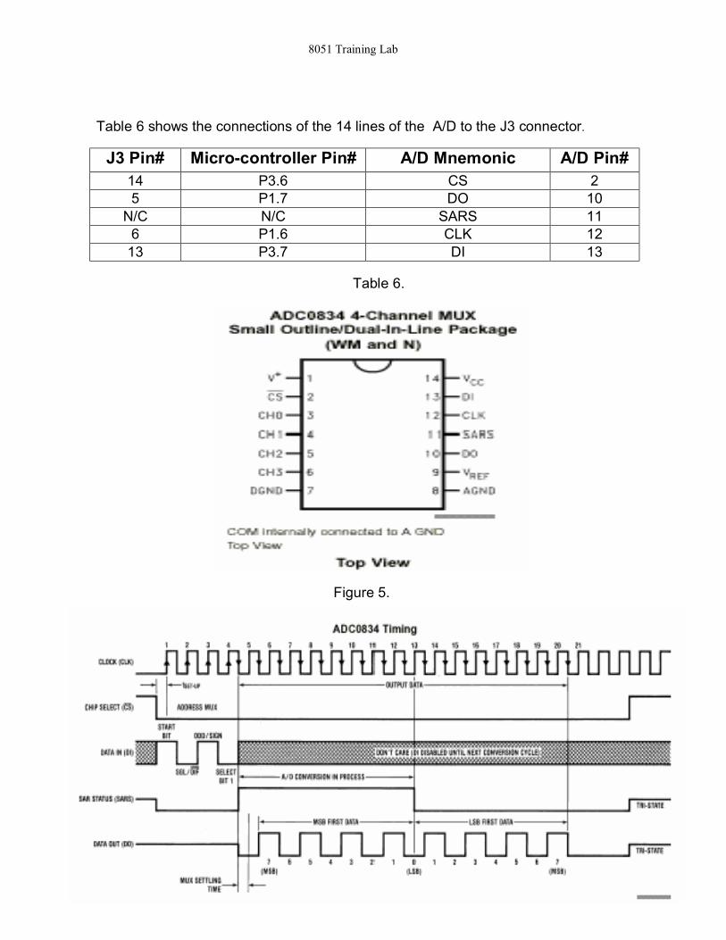
Table 6 shows the connections of the 14 lines of the A/D to the J3 connector.
J3 Pin# Micro-controller Pin# A/D Mnemonic A/D Pin# 14 P3.6 CS 2 5 P1.7 DO 10
N/C N/C SARS 11 6 P1.6 CLK 12
13 P3.7 DI 13 Table 6.
Figure 5.

8051 Training Lab
Page 18
Figure 6. Figure 7. Pin 3 of the A/D receives the Analog input voltage signal. A DC Voltmeter when placed on Pin 3 should read between VCC and GND as the potentiometer is varied from one extreme to the other as shown in Figure 7. The LM35 temperature sensor will also be connected to this input later. The A/D converter consists of 4-input multiplexed analog channels, which may be software configured as 4 single-ended channels or 2 differential channels, or a new pseudo differential option. The input format is assigned during MUX addressing sequence prior to start of conversion and this selects the analog input and their mode (single or differential).
To Pin 3 of A/D. Ch0 X1.1 on TB-1
VCC
GND
10 K ohm variable potentiometer
8051 Training Lab
Page 19
Steps for A/D Conversion • Initially the DI and CS inputs must be high. • Pull the CS (chip select) line low and must be held low for the entire duration of the
conversion. The converter is waiting for the Start bit and the MUX assignment. • A clock is generated by the processor and output to the A/D clock input. • The start bit is a logic “1” on the DI input line, after which the MUX assignment word on
the DI line is presented. The status of the DI line is clocked on each rising edge of the clock line.
• The SARS status output line from the A/D goes high, indicating that a conversion is now in progress and the DI line is disabled.
• The data out (DO) line comes out of Tri-state and provides a leading zero for one clock period.
• After 8 clock periods the conversion is complete. The SARS line returns low ½ clock cycle later.
• The DO line now generates the binary equivalent of the analog value as 8 output bits with LSB first. The DO line than goes low and remains low until chip select (CS) is made to go high. This clears all the internal registers and another conversion may now be started by making the CS go low again and repeating the process.
Exercise Write a C program that uses the A/D in single ended mode with the potentiometer connected to Channel 0 or Pin3 on the A/D through the terminal block on the TB-1 board. Vary the analog input voltage and display the value on the screen. Then, connect the potentiometer to Pin4 also and display its value. Connect the temperature sensor to Pin3 and potentiometer to Pin4 and display both the values simultaneously on the terminal screen.

8051 Training Lab
Page 20
LAB5 – Analog To Digital Conversion on Mini-Max/51-C2 Overview The purpose of this lab is to familiarize you with the 10-bit ADC on PIC16F818 embedded on MINI-MAX/51-C2 board. The potentiometer (that we used in Lab4) is connected to Analog Port Terminal on MINI-MAX/51-C2. Measurement results for all 5 channels will be displayed in the terminal screen. Information The secondary micro-controller PIC16F818 embedded on MINI-MAX/51-C2 board works as an I2C slave peripheral device and can provide 5-channel 10-bit ADC using 5V internal or 4.096V external voltage reference source. PIC16F818 has I2C device address 0xB0 , A/D control register address - 0x17 and data register address-0x18. A/D Control register description
Bit Description 7 ADFM: A/D Result Format Select bit
1 = Right justified, 6 Most Significant bits of ADRESH are read as ‘0’ 0 = Left justified, 6 Least Significant bits of ADRESL are read as ‘0’
6 ADCS2: A/D Clock Divide by 2 Select bit 1 = A/D Clock source is divided by 2 when system clock is used 0 = Disabled
5-4 ADCS1:ADCS0: A/D Conversion Clock Select bits If ADSC2 = 0: 00 = FOSC/2 01 = FOSC/8 10 = FOSC/32 11 = FRC (clock derived from the internal A/D module RC oscillator) If ADSC2 = 1: 00 = FOSC/4 01 = FOSC/16 10 = FOSC/64 11 = FRC (clock derived from the internal A/D module RC oscillator)

8051 Training Lab
Page 21
A/D Control register description-continue
Bit Description 3-0 PCFG<3:0>: A/D Port Configuration Control bits
PCFG AN4 AN3 AN2 AN1 AN0 VREF+ VREF- C/R 0000 A A A A A AVDD AVSS 5/0 0001 A V+ A A A AN3 AVSS 4/1 0010 A A A A A AVDD AVSS 5/0 0011 A V+ A A A AN3 AVSS 4/1 0100 D A D A A AVDD AVSS 3/0 0101 D V+ D A A AN3 AVSS 2/1 011x D D D D D AVDD AVSS 0/0 1000 A V+ V- A A AN3 AN2 3/2 1001 A A A A A AVDD AVSS 5/0 1010 A V+ A A A AN3 AVSS 4/1 1011 A V+ V- A A AN3 AN2 3/2 1100 A V+ V- A A AN3 AN2 3/2 1101 D V+ V- A A AN3 AN2 2/2 1110 D D D D A AVDD AVSS 1/0 1111 D V+ V- D A AN3 AN2 1/2
Legend: A = Analog input D = Digital I/O V+ = VREF+ V- = VREF- C/R = Number of Analog input channels/Number of A/D Voltage references Exercise Write a C program that uses built-in 10-bit ADC on PIC16F818 embedded on MINI-MAX/51-C2 board, reads all 5 channels and displays their values on the terminal screen. Connect the potentiometer consistently to the each of analog inputs, vary the analog input voltage and observe results.

8051 Training Lab
Page 22
LAB6 – Timers and Interrupts Overview This lab is designed to familiarize the student with timers and interrupts. External interrupts on switch closures are generated and back ground timers are made to run for timing certain external events. The switch and the LED’s for this experiment are already present on the TB-1 board. Results will be displayed on the terminal screen. Information The 8051 training kit uses the AT89C51ED2 micro-controller. A brief overview of the interrupts on this micro-controller is given below: An interrupt is executed when the micro-controller stops its normal code and branches to a predefined section of the memory to execute specific instructions. After this it goes back to its normal operation from where it had left before. Six interrupt vectors are present on the micro-controller: • Two external interrupts INT0 and INT1 • Three timer interrupts Timer0, Timer1, Timer2 • One serial interrupt. Each of these interrupt sources can be individually enabled or disabled by setting or clearing a bit in the Special Function Register IE which also contains global disable bit EA which disables or enables all the interrupts at once. INT0 and INT1: First exercise is to generate an external interrupt INT0 which is tied to port P3.2 (SW1 on TB-1). A change in the logic level of P3.2 will generate an interrupt in the program. Table 7. defines the registers and the bits that are used for controlling external interrupt 0 (INT0). The same holds true for INT1 except instead of IT0, IE0 and EX0 consider IT1, IE1 and EX1 and port number is P3.3 (SW2 on the TB-1). INT0 Register BIT Description TCON IT0 Set than low level triggered, clear than edge triggered TCON IE0 Set by micro-controller when interrupt occurs and than automatically
cleared when interrupt is processed IE EA Set to enable global interrupt IE EX0 Set to enable external interrupt Table 7.

8051 Training Lab
Page 23
Every time SW1 is pressed on TB-1 (so that port pin P3.2 on the micro-controller is logic low) , the micro-controller will generate an interrupt and an action will occur, e.g. incrementing a counter and displaying its value on the terminal screen. Timer0 Register TMOD is the timer counter mode control register and the TCON register turns the timer On/Off and indicates an overflow by setting a flag bit. Register Bit Description TCON TR0 Set indicates Timer0 is On, clear indicates Timer0 is Off IE EA Set indicates Global Interrupt is enabled TCON TF0 Set by the micro-controller when Timer0 overflows, cleared by the
micro-controller when vectored to the interrupt service routine The TMOD register enables the user to select different modes of operation for Timer 0 and Timer 1. Write a program to run a background timer of 30 milliseconds. Every time the 30-millisecond period is over, the program will jump to an interrupt routine and toggle the state of an I/O (P1.3 Red LED) line so the Red LED will blink every 30 milliseconds. To further expand the program, a counter should also be incremented in the interrupt routine. When the counter exceeds a certain value (e.g. 1000) another I/O line (P1.1 Yellow LED) should toggle and the counter should reset back to zero (1000 * 30 milliseconds = 30,000 milliseconds = 30 seconds ). Second LED will blink On and Off every 30 seconds which can be easily monitored using a wrist-watch or PC’s clock. The same can be done with Timer1 where by TR1 and TF1 are used. IE Register
Bit # Mnemonic Description IE.7 (MSB) EA Global Interrupt Enable. IE.6 ------ Not Implemented IE.5 ET2 Timer2 interrupt enable bit. IE.4 ES Serial Port interrupt enable IE.3 ET1 Timer1 interrupt enable bit IE.2 EX1 External Interrupt 1 enable bit IE.1 ET0 Timer0 interrupt enable bit IE.0 (LSB) EX0 External Interrupt 0 enable bit Enable Bit = 1 enables the interrupt Enable Bit = 0 disables the interrupt

8051 Training Lab
Page 24
TCON Register
Bit # Mnemonic Description TCON.7 (MSB) TF1 Timer1 Overflow flag TCON.6 TR1 Set indicates Timer1 is On and Clear indicates Timer1 is Off TCON.5 TF0 Timer0 Overflow flag TCON.4 TR0 Set indicates Timer0 is On and Clear indicates Timer0 is Off TCON.3 IE1 Set by micro-controller when Timer1 interrupt occurs and
cleared by micro-controller when interrupt is processed TCON.2 IT1 Set than low level triggered, clear than edge triggered TCON.1 IE0 Set by micro-controller when Timer0 interrupt occurs and
cleared by micro-controller when interrupt is processed TCON.0 (LSB) IT0 Set than low level triggered, clear than edge triggered

8051 Training Lab
Page 25
LAB7 - 4x4 Keypad Overview Student connects a keypad to the keypad connector on the MicroTRAK Carrier Board and programs the keypad. Information The MicroTRAK Carrier Board has a 10-pin keypad connector, which is connected to Port 2 of the micro-controller. The pin-out of the connector is shown below in Table 8.
Micro-controller Port Pin Keypad Connector Pin# P2.0 1 P2.1 2 P2.2 3 P2.3 4 P2.4 5 P2.5 6 P2.6 7 P2.7 8 Gnd 9 Vcc 10
Table 8. Many keypads are wired as a matrix of rows and columns. The internal connections of a 4 -row by 4-column keypad are shown in Figure 8.

8051 Training Lab
Page 26
1K 1K 1K 1K
VCC
ROW 1
ROW 2
ROW 3
ROW 4
COLUMN 1
COLUMN 2
COLUMN 3
COLUMN 4
Figure 8.

8051 Training Lab
Page 27
Matrix connection saves on the number of connections and micro-controller port lines. For example, a 4-row by 4-column keypad would require 17 wires (16 + ground) if each key was individually connected to micro-controller ports. Using the matrix approach and scanning the keypad under software control reduces the number of wires and port pins to 8 ( 4 rows + 4 columns ). When a key is pressed, the row for that key will be physically connected to the column for that key. Therefore, the port input for the column will be at the same logic level as the port output for the row. Since the columns (inputs) are normally at the HIGH logic level due to pull-up resistors, the only way to make a column LOW will be to press a key and make the row for that key LOW. By periodically strobing each row LOW one row at a time, and reading the column input levels during each strobe, one can determine which key is pressed. This is illustrated by Table 9 for the 4 by 4 keypad. In the Row Mask, Row 1 is assigned to the Most Significant Bit and Row 4 is assigned to the Least Significant Bit. Similarly in the Column Mask, Column 1 is assigned to the Most Significant Bit and Column 4 is assigned to the Least Significant Bit.
Action Row Mask Column Mask No keys were pressed XXXX 1111 Row 1 Column 1 key pressed 0111 0111 Row 1 Column 2 key pressed 0111 1011 Row 1 Column 3 key pressed 0111 1101 Row 1 Column 4 key pressed 0111 1110 Row 2 Column 1 key pressed 1011 0111 Row 2 Column 2 key pressed 1011 1011 Row 2 Column 3 key pressed 1011 1101 Row 2 Column 4 key pressed 1011 1110 Row 3 Column 1 key pressed 1101 0111 Row 3 Column 2 key pressed 1101 1011 Row 3 Column 3 key pressed 1101 1101 Row 3 Column 4 key pressed 1101 1110 Row 4 Column 1 key pressed 1110 0111 Row 4 Column 2 key pressed 1110 1011 Row 4 Column 3 key pressed 1110 1101 Row 4 Column 4 key pressed 1110 1110 Table 9.

8051 Training Lab
Page 28
Port2 is connected to the Keypad connector with the configuration shown in Table 10.
Port2.0 Row1 Output Port2.1 Row2 Output Port2.2 Row3 Output Port2.3 Row4 Output Port2.4 Column 1 Input Port2.5 Column 2 Input Port2.6 Column 3 Input Port2.7 Column 4 Input
Table 10. In the port direction register, the port pins connected to rows are defined as outputs and the port pins connected to columns are defined as inputs. Each key on the keypad is assigned a given value by the programmer before hand. The Keypad algorithm can be based on the following rules. Algorithm • A Column is generally high (output). • One row at a time is made to go low (input) and than the columns are read. • If one or more columns are low than the switches of the corresponding columns are
active and their respective values should be displayed on the terminal. Exercise Determine the pin-out and the matrix layout of your keypad using the ohmmeter function of your multi-meter. Write a C program that displays – on the terminal screen- the key being pressed on the keypad.

8051 Training Lab
Page 29
LAB8 – Liquid Crystal Display (LCD) Overview This Lab familiarizes the student with industry-standard alphanumeric LCD’s by connecting the LCD to the LCD connector of the 8051 training kit and writing a program in C to display various characters using 4-bit mode. Information Dot matrix LCD displays are readily available from many companies such as Sharp, Hitachi and OPTREX. The LCD’s generally come in display formats of 16 X 1, 16 X 2, 24 X 2 and 40 X 4 (column X row). These typically have 8 data lines DB0 – DB7 ( Data 0 through Data 7 ), VCC (Power), GND (Ground), RS (Register Select), R/W (Read/Write), E (Enable). This exercise will use a 24 X 2 display, to be connected to the LCD connector. The three control lines are explained below. RS Register Select Control 1 = LCD in data mode 0 = LCD in command mode E Data / Control state Rising Edge = Latches control state Falling Edge = Latches data R/W Read / Write control 1 = LCD to write data 0 = LCD to read data In the 4-bit mode, data is transferred either on the lower or upper nibble of the port, this saves in I/O lines but the program occupies more space as two commands are required to display a character.

8051 Training Lab
Page 30
Table 11. shows the connection between the display and the LCD connector in 4-bit mode with low nibble. LCD Connector
Pin# Micro-controller
Pin LCD Display
Pin LCD Display
Pin# 1 GND GND 1 2 VCC VCC 2 3 Vee(PIC) VEE 3 4 P0.0 RS 4 5 P0.1 R/W 5 6 P0.2 E 6 7 not connected not connected 7 8 not connected not connected 8 9 not connected not connected 9
10 not connected not connected 10 11 P0.4 DB4 11 12 P0.5 DB5 12 13 P0.6 DB6 13 14 P0.7 DB7 14
Table 11. Exercise Using the LCD datasheet, write a C program that displays “Hello World” on the first row of the LCD. Then, display the same message on the second row of the LCD.
8051 Training Lab
Page 31
LAB9 - How to adjust LCD contrast
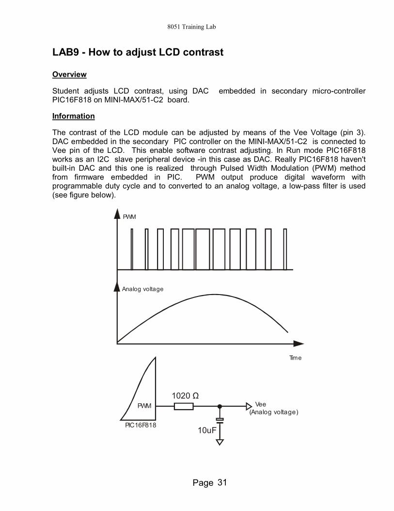
Overview Student adjusts LCD contrast, using DAC embedded in secondary micro-controller PIC16F818 on MINI-MAX/51-C2 board. Information The contrast of the LCD module can be adjusted by means of the Vee Voltage (pin 3). DAC embedded in the secondary PIC controller on the MINI-MAX/51-C2 is connected to Vee pin of the LCD. This enable software contrast adjusting. In Run mode PIC16F818 works as an I2C slave peripheral device -in this case as DAC. Really PIC16F818 haven't built-in DAC and this one is realized through Pulsed Width Modulation (PWM) method from firmware embedded in PIC. PWM output produce digital waveform with programmable duty cycle and to converted to an analog voltage, a low-pass filter is used (see figure below).
PIC16F818
PWM1020 Ω
Vee
10uF
(Analog voltage)
Time
Analog voltage
PWM

8051 Training Lab
Page 32
Embedded in PIC firmware has two PWM modes - 4 bits and 10 bits PWM. For setting 4 bit PWM value you should send numeric value from 0 to 15 to the PIC device only .
4 bits PWM 0 0 0 0 PWM3 PWM2 PWM1 PWM0
For 10 bits PWM you should to send as first byte higherest 4 bits from needed 10 bit PWM value and after that you should send lowest 6 bits + 0x40 as second byte.
10 bits PWM first byte 0 0 0 0 PWM9 PWM8 PWM7 PWM6
second byte 0 1 PWM5 PWM4 PWM3 PWM2 PWM1 PWM0 Exercise Write a C program that uses 4 bits PWM for contrast adjusting and displays on the first row of the LCD the current contrast. Expand the program with using 10 bits PWM.

8051 Training Lab
Page 33
LAB10 - Buzzer
Overview Student programs the buzzer on the TB-1 to generate different notes using software. Student then generates a little musical piece using the notes that he/she programmed. Information A buzzer or simple speaker will generate music when a series of square waves is applied to its positive input with the negative grounded. The frequency of the square wave should be less than 12KHz to be audible. Varying the frequency of the square wave will generate different musical tones. The buzzer on the TB-1 is connected to port pin P1.2 on the micro controller. This pin needs to be programmed as an output pin and square waves of varying frequencies and duty cycle need to be generated. Exercise • Program P1.2 on the micro-controller as an output pin • Decide a time period or frequency of square wave between 1KHz to 15KHz. • Generate a signal of 50% Duty cycle, where
Duty Cycle = On Time / (On Time + Off Time) of square wave. • Activate buzzer for approx 5 to 10 seconds • Change frequency of buzzer and note the different sound • Change only duty cycle and note the different intensity.
![Leaf Me Alone Labbook[1]](https://static.fdocuments.in/doc/165x107/54103b277bef0a3b0a8b4724/leaf-me-alone-labbook1.jpg)